a multi-fpga networking architecture and its implementation
TRANSCRIPT

A MULTI-FPGA NETWORKING ARCHITECTURE AND ITS IMPLEMENTATION
A Thesis
by
GABRIEL SCANNELL KNEZEK
Submitted to the Office of Graduate and Professional Studies of
Texas A&M University
in partial fulfillment of the requirements for the degree of
MASTER OF SCIENCE
Chair of Committee, Jyh-Charn (Steve) Liu
Committee Members, Duncan Henry M. Walker
Sunil Khatri
Radu Stoleru
Head of Department, Dilma Da Silva
May 2015
Major Subject: Computer Engineering
Copyright 2015 Gabriel Scannell Knezek
ii
ABSTRACT
FPGAs show great promise in accelerating compute-bound parallelizable
applications by offloading kernels into programmable logic. However, currently FPGAs
present significant hurdles in being a viable technology, due to both the capital outlay
required for specialized hardware as well as the logic required to support the offloaded
kernels on the FPGA. This thesis seeks to change that by making it easy to communicate
clusters of FPGAs over IP networks and providing infrastructure for common
application use cases, allowing authors to focus on their application and not the
procurement and details of interacting with a specific FPGA.
Our approach is twofold. First, we develop an FPGA IP network stack and bitfile
management system allowing users to upload their logic to a server and have it run on
FPGAs accessible through the Internet. Second, we engineer a programmable logic
interface which authors can use to move data to their application kernels. This interface
provides communication over the Internet as well as the scaffolding typically re-invented
for each application by providing I/O between application logic, even if spread across
different FPGAs.
We utilize Partial Reconfiguration to divide the FPGAs into regions, each of
which can host different applications from different users. We then provide a web
service through which users can upload their FPGA logic. The service finds a spot for
the logic on the FPGAs, reconfigures them to contain the logic, then sends back the user
their IP addresses.

iii
To ease development of the application pieces themselves, our framework
abstracts away the complexity of communicating over IP networks as well as between
different FPGAs. Instead we provide an interface to applications consisting simply of a
RAM port. Applications write packets of data into the port, and they appear at the other
end, whether that other end is across an IP network or another FPGA.
Finally, we then prove the feasibility and utility of our approach by implementing
it on an array of Xilinx Virtex 5 FPGAs, linked together with GTP serial links and
connected via Gigabit Ethernet. We port a compute-bound application based on regular
expression string matching to the framework, demonstrating that our approach is feasible
for implementing a realistic application.

iv
ACKNOWLEDGEMENTS
I would like to thank my committee chair, Dr. Steve Liu, for his guidance,
support and patience throughout this process, as well as my committee members, Dr.
Walker, Dr. Khatri, and Dr. Stoleru.
Thanks also go to the department faculty and staff for their support and making
my time at Texas A&M University a great experience.
Finally, thanks to my family and close friends for their boundless
encouragement, patience, and belief in me.

v
NOMENCLATURE
API Application Program Interface
ARM Advanced RISC Machines
ARP Address Resolution Protocol
ASIC Application Specific Integrated Circuit
AXI Advanced Extensible Interface
CLB Configurable Lookup Block
CPU Central Processing Unit
CRC Cyclic Redundency Check
CUDA Compute Unified Device Architecture
DMA Direct Memory Access
DRAM Dynamic Random Access Memory
FIFO First-In First-Out
GPU Graphics Processing Unit
GigE Gigabit Ethernet
HDL Hardware Description Language
HPC High Performance Computing
HTTP Hypertext Transfer Protocol
I/O Input/Output
ICAP Internal Configuration Access Port
IOCTL Input/Output Control
vi
IP Internet Protocol
IP core Intellectual Property Core
JTAG Joint Test Action Group
KVM Kernel-Based Virtual Machine
LUT Look-Up Table
MAC Media Access Control
MPI Message Passing Interface
MUX Multiplexor
NFA Non-deterministic Finite Automata
NOC Network-on-Chip
OS Operating System
PC Personal Computer
PCIe Peripheral Component Interconnect Express
PHY Physical Transciever
PR Partial Reconfiguration
PROM Programmable Read Only Memory
RAM Random Access Memory
SATA Serial Advanced Technology Attachment
SDK Software Development Kit
SRAM Static Random Access Memory
TCP Transport Control Protocol
UDP User Datagram Protocol

vii
XML Extensible Markup Language
YAML Yet Another Markup Language

viii
TABLE OF CONTENTS
Page
ABSTRACT .............................................................................................................. ii
DEDICATION .......................................................................................................... iii
ACKNOWLEDGEMENTS ...................................................................................... iv
NOMENCLATURE .................................................................................................. v
TABLE OF CONTENTS .......................................................................................... viii
LIST OF FIGURES ................................................................................................... x
LIST OF TABLES .................................................................................................... xii
1. INTRODUCTION ............................................................................................... 1
2. BACKGROUND AND RELATED WORK ....................................................... 4
3. DESIGN OVERVIEW ........................................................................................ 11
3.1 Supporting Infrastructure ..................................................................... 14
4. DESIGN .............................................................................................................. 16
4.1 FPGA Application Interface ................................................................. 16
4.2 Interface to the FPGA Network ........................................................... 23
4.3 Framework Data Transport Overview .................................................. 26
4.4 Off-Chip Communication Methods ..................................................... 28
4.4.1 Internet ........................................................................................ 28
4.4.2 Locally ......................................................................................... 32
4.5 Data Movement between Pieces and Off-Chip Links .......................... 34
4.5.1 Connecting Pieces and Off-Chip Links ....................................... 34
4.5.2 Data Buffering ............................................................................. 36
4.5.3 Switching ..................................................................................... 39
4.6 Routing Incoming Ethernet Packets to Pieces ...................................... 43
4.7 Off-Chip Piece-to-Piece Routing ......................................................... 44
4.8 Application Piece Placement and Configuration.................................. 48
4.8.1 Placement Algorithm ................................................................... 48

ix
Page
4.9 Configuring the FPGA Network to Contain an Application ................ 51
4.9.1 Configuration Algorithm ............................................................. 52
4.10 Partial Reconfiguration Engine ............................................................ 52
4.10.1 Introduction to Partial Reconfiguration ..................................... 53
4.10.2 Technology Background ........................................................... 54
4.10.3 Existing Implementations .......................................................... 56
4.10.4 Our Design ................................................................................ 57
4.10.4.1 Piece Gating .................................................................. 57
4.10.4.2 Architecture ................................................................... 59
5. IMPLEMENTATION AND EVALUATION .................................................... 63
5.1 Implementation Overview .................................................................... 64
5.2 Data Movement through the Framework ............................................. 66
5.3 Ethernet Frontend ................................................................................. 73
5.4 ARP Resolution .................................................................................... 76
5.5 Inter-FPGA Serial Input Frontend ........................................................ 78
5.6 Inter-FPGA Connection Topology ....................................................... 79
5.7 First Level Mux .................................................................................... 80
5.8 Second Level Mux ............................................................................... 81
5.9 Piece-to-Piece Switch ........................................................................... 82
5.10 PR Slot Wrapper – Ethernet Portion .................................................... 85
5.11 PR Slot Wrapper – Piece-to-Piece Portion ........................................... 88
5.12 Client Interface ..................................................................................... 90
4.12.1 Build System ............................................................................. 92
5.13 Evaluation ............................................................................................. 94
5.13.1 Performance Metrics ................................................................. 94
5.13.1.1 Logic Availability ......................................................... 98
5.13.1.2 Reconfiguration Time ................................................... 98
5.13.12 Example Application ............................................................... 99
6. SUMMARY OF FUTURE WORK .................................................................... 105
6.1 Security and Reliability ........................................................................ 105
6.2 Scaling to 10 Gigabit Ethernet ............................................................. 107
REFERENCES .......................................................................................................... 109
APPENDIX A: INTRODUCTION TO HIGH-SPEED SERIAL CONNECTIONS 114
APPENDIX B: TECHNICAL DETAILS OF EXTENDING CES ACROSS
MULTIPLE PIECES ........................................................................................... 117
x
LIST OF FIGURES
FIGURE Page
1 High-Level Operational Overview of the Proposed Multi-FPGA
Architecture ................................................................................................ 23
2 Data Interface between Architecture and Application Piece...................... 23
3 Example Application Piece Interconnections............................................. 25
4 Example Application Piece Physical Placement ........................................ 26
5 Partitioned Multiple RAM Design with 2 Level Data Source MUX ......... 39
6 Example of Piece-to-Piece Routing Implementation ................................. 42
7 Routing Application Data through Intermediate FPGA ............................. 47
8 Packet Dataflow during PR Slot Gating ..................................................... 62
9 Overview of Framework Implementation .................................................. 65
10 Detailed Overview of Framework Components ......................................... 66
11 Flow Control Model ................................................................................... 70
12 Go/Done Flow Control ............................................................................... 71
13 Go/Ready Flow Control ............................................................................. 71
14 Data Transport from Frontend to Application Piece .................................. 72
15 Data Transport from Piece to Piece via Copying Module.......................... 73
16 Frontend Module Dataflow Diagram ......................................................... 75
17 Combined Verification Unit and PR Slot Wrapper Approach ................... 82
18 Data Flow through Switch Frontend to Piece ............................................ 84
19 Incoming Concurrent Packet Verification Engine ..................................... 87

xi
FIGURE Page
20 Sample Application Configuration File ..................................................... 91
21 Example Inter-FPGA Relay Test Application ........................................... 97
22 CES String Matching Operation ................................................................ 101
23 Pipelining Approach to Partitioning CES across Pieces ............................ 102
xii
LIST OF TABLES
TABLE Page
1 RAM Interface Signals – Incoming Port .................................................... 22
2 RAM Interface Signals – Outgoing Port .................................................... 22

1
1. INTRODUCTION
Field Programmable Gate Arrays (FPGAs) are a class of integrated circuit chips
known as programmable logic. Fundamentally, FPGAs consist of a large quantity of
identical look up tables (LUTs) and a matrix of wires interconnecting these LUTs. Both
the contents of the LUTs and the connection of wires in the matrix are quickly
programmable at runtime by downloading new configurations to the chip.
The ability to reprogram the elements of the FPGA gives rise to the name
programmable logic and allows FPGAs to implement a variety of digital logic circuitry.
Invented in the 1980’s, FPGAs have steadily increased in the amount of digital logic
they can implement, and are now widely used in industry and the subject of much active
research due to several unique features they enable. One application is in the design of
ASICs. FPGAs enable low-volume production runs of chip designs for prototyping and
debugging at a fraction of the cost of ASIC fabrication. Furthermore, the runtime re-
configurability of FPGAs is useful in situations where the final specification for the
digital design is still evolving or is in the process of standardization.
Another increasingly popular use is as a platform for accelerating compute-
bound parallelizable applications. With FPGAs, the parallelizable kernel of an algorithm
can be coded in a hardware description language, then duplicated across the logic fabric
of the FPGA many times. Such replication can often offer an order of magnitude or more
processing throughput as compared with CPU-based implementations.

2
Another platform for parallelizable application acceleration are General Purpose
GPUs (GPGPUs). These are GPUs in which the computation performed by the GPU’s
shader units can be programmed with arbitrary algorithms. Since GPUs contain many
shader units which run in parallel, by re-writing their application’s algorithms to run as a
shader, users can achieve similar parallel speedups. GPGPUs are often chosen for an
application accelerator platform over FPGAs even though their rigid shader structure
often imposes limitations which are nonideal for the algorithm being accelerated. This is
due to the fact that as compared with FPGAs, GPGPUs are cheaper and already present
in existing PCs, as well as the fact that GPGPU programming APIs provide mechanisms
for software to easily move data from their application running on the PC to the
accelerated kernel on the GPGPU. FPGAs, in comparison, are more expensive than
GPGPUs and have a single purpose as the application accelerator: since they aren’t
already usable as the graphics card for a PC, for a prototype, it can be a riskier purchase
to acquire a number of FPGAs for a single application which may or may not see
benefits. A bigger problem with FPGAs is the lack of supporting libraries and toolchains
to easily move data between the application running on a PC and the accelerated kernel
on the FPGA. The user is often presented with a blank slate, and must re-invent the
wheel. This is as opposed to GPGPUs, where several relatively mature programming
languages (CUDA, OpenCl, DirectX Compute Architecture) provide simple APIs to
transfer data and schedule the accelerated kernel for execution on the GPU.
The goal of this thesis is to change this current state of affairs by providing the
infrastructure to make it as easy to run pieces of an application on an FPGA in an

3
accelerated fashion as it currently is on a GPGPU. We do this in two ways. First, by
removing the high cost entailed in getting started with FPGAs through creating a cloud
computing architecture for FPGAs, allowing users to utilize as little or as much FPGA
resources as required only for the period of time their application is running. Second, by
creating interfaces for moving data between the majority of an application running on a
PC and the accelerator on the FPGA in the cloud that are easy to use and are high
performance, so the user only needs to focus on writing the application algorithm in
programming logic itself.

4
2. BACKGROUND AND RELATED WORK
The concept of offering computing resources accessible over a network is a trend
that has been ongoing in the PC industry for a long time. Popular examples of companies
which sell computing accessible over the Internet include Amazon’s EC2 service [1],
Google’s AppEngine [2], and Microsoft’s Azure [3]. For example, at the user's request,
Amazon EC2 provides IP connectivity to PCs hosted in their datacenters. Google App
Engine provides a different approach, closer to the model our thesis aims to provide for
FPGAs. Instead of offering access to PCs directly and requiring the user to manage OS
installation, application inter-PC communication, etc, App Engine restricts the user to
running their application in the form of a sandboxed Java application. In return for this
restriction, App Engine is provided an API for easily communicating with users via the
web, as well as managing I/O in the form of both persistent storage and communication
between application components.
Ken Eguro et al. also propose using FPGAs in a environment where shared
servers are accessible over the network, but for a different aim than our thesis. Instead of
offering access to a network of FPGAs for the purpose of commoditizing access to
parallel computing resources, they propose adding FPGA cards to traditional PC servers
in a datacenter. These FPGAs can then be accessed securely, sandboxed from other users
of the PC by applications with high security requirements [4].
Similarly, much research is being performed in the areas of linking FPGAs
together with serial-links, high-speed communication between PCs and FPGAs (either
through Ethernet or PC-local busses), on-chip routing architectures, and partial

5
reconfiguration. One such project is [5]. They describe a similar system to this thesis,
providing reconfigurable regions in FPGAs to clients running in virtual machines in the
cloud over Ethernet. In contrast to our approach, they tightly integrate their FPGAs into
an existing OpenStack cloud computing cluster, and require hardware accelerators
running on the FPGAs to deal with raw Ethernet frames instead of handling UDP in the
framework. Finally, they do not inter-connect the FPGAs together with a separate high-
bandwidth serial network for supporting accelerators which require more resources than
a single FPGA can provide.
Another project is [6]. This project connects FPGAs to PC servers in a cloud
computing infrastructure over the PCI Express (PCIe) bus. The servers are running the
para-virtualization software KVM, hosting multiple client operating systems. The
authors propose a system where the hypervisor treats the FPGA in a similar manner to a
network card. The FPGA contains a PCIe DMA engine for copying job information and
buffers between the PC’s memory and user accelerators running on the FPGA. Guest
virtual machines (VMs) interface with the FPGA accelerators using Linux IOCTLs
which move buffers of data between the guest VM and the FPGA. To provide a
complete system, they also briefly touch on an implementation for storing bitfiles
received from guest OSes and configuring them on to the FPGAs, although they do not
go into detail. The FPGAs themselves are partitioned into PR regions, each of which can
host different hardware pieces from different users simultaneously, with a management
agent in the hypervisor deciding which user accelerator is run at what time. This project
shares our ideas of providing abstract reconfigurable regions of programmable logic to

6
users and managing storage and placement of the programmable logic bitfiles. It
implements the concept of providing a simple buffer-based interface to software running
on a PC through which it communicates with the FPGAs. However, it is substantially
different from our approach in that it tightly couples the FPGAs to individual servers in
the cloud over the PC local bus PCIe, and does not provide provisions for spanning
hardware accelerators across multiple FPGAs. Also, the API provided to this project is
in the form of Linux IOCTLs specific to the KVM hypervisor. Our approach, while
potentially less straightforward to program, is much more general, and can be used with
any operating system or application supporting sockets.
With regard to inter-FPGA serial links, it’s becoming increasingly common to
build clusters of FPGAs linked together with high speed serial links. Some projects use
partial reconfiguration; others configure the entire FPGA with a single application. A
few projects are presented below; however, universally they focus on the acceleration of
a single application in an attempt to achieve high performance computing. Usually,
management of the FPGAs over Ethernet is neglected entirely from the discussion, and
in every case the goal is not on sharing the infrastructure among multiple applications
and users via the Internet.
One such project, Catapult [7], describes the experiences of a team in Microsoft
Research building a hardware accelerator system to increase the performance of Bing’s
search ranking algorithms. As part of that project, they construct a system with FPGAs
linked to one another via high-speed serial channels in a torus topology. Each FPGA is
connected to a single server in the datacenter via PCI Express (PCIe). Each FPGA hosts

7
a single application; in their model, an application is typically large enough to span
multiple FPGAs, so subdividing the FPGA into reconfigurable pieces was not a design
requirement of the project. The FPGA is not partially reconfigurable with new
applications. However, it follows a similar design as other projects which are
reconfigurable. Surrounding the application portion of the FPGA is service layer which
manages interactions with the PC, routing packets to other FPGAs and interactions with
on-board memory. Very brief treatment is given to the mechanism of routing between
FPGAs, but data is packetized and routing is determined statically by the non-FPGA
portion of the accelerated application. Their project does not focus on connecting the
FPGAs over Ethernet nor using PR regions.
Another project, the Reconfigurable Computing Cluster [8, 9], aims to use
FPGAs to build a cost effective supercomputer capable of executing a PetaFLOP of
computing. They have constructed a 64 node FPGA cluster using Virex4 FPGAs.
Similar to our design, they interconnect their FPGAs with serial links using the Aurora
protocol, and provide routing between pieces of computational logic both within a single
FPGA and across their network of FPGAs. However, their design is focused around
providing a cluster of FPGAs for high performance computing, not providing FPGAs as
a service for multiple users simultaneously. Their architecture is centered around the
PowerPC CPUs contained within each FPGA, with reconfigurable computing connected
as processor peripherals. Also, their primary means of exchanging data is via the serial
links; their Ethernet connection is used for administrative tasks. In contrast, our design
uses Ethernet as key means of communication between users and the FPGAs.

8
The Maxwell project focused on creating a grid of FPGAs in support of HPC
[10], from the University of Edinburgh. Similar to the Reconfigurable Computing
Cluster (RCC), they constructed a network of 64 FPGAs, interconnected with serial
links, and employ a hybrid CPU-FPGA compute structure. Unlike the RCC, they use
separate CPUs not embedded in the FPGAs: their grid consists of 32 Intel Xeon servers,
each of which hosts two FPGAs connected with PCI express. In their machine,
computation of their example applications occurs on these servers. Applications use an
MPI style interface to interact with offloaded computation kernels using software
libraries they have constructed called the Parallel Toolkit. Unlike the RCC, their inter-
FPGA links do not provide routing; the point-to-point connections between FPGAs are
directly exposed to the applications, which must implement their own routing if needed.
Similar to the RCC, the authors focus on the HPC aspects of their machine, devoting it
entirely to the service of a single application and avoiding details of configuration and
remote interaction.
A further application-specific 64-node cluster created by the University of
Cambridge is Bluehive [11]. In contrast to the previously mentioned systems, Bluehive
does not pair each FPGA with a hard or soft-core CPU. Instead, the entire FPGA is
dedicated to their neural network simulator. Like previous designs, they interconnect
their FPGAs with serial links, in this case with a 3-D topology. Custom System Verilog
logic provides routing among the serial channels. Although they have open-sourced
many aspects of the design, they have not set out to design a general purpose framework
nor one which can be dynamically reconfigured.

9
Finally, the Formic project [12] constructed their own development boards based
on Xilinx Spartan 6 FPGAs with the goal of reducing the cost of assembling multi-
FPGA clusters. Like previous designs, they constructed a 64 node cluster. Each board
contains 8 serial links, and are interconnected in a 3D configuration. They use this
cluster to prototype a new manycore CPU architecture. Reconfiguration and support for
multiple applications at once are not discussed.
Other current research focuses on providing Ethernet interfaces for applications
running on a single FPGA and on reconfiguring FPGA bitstreams remotely, but do not
address interconnecting FPGAs together. The SIRC project from Microsoft Research
[13] is one such approach, providing an interface for computational kernels running on
an FPGA to interface with applications on a PC via gigabit Ethernet. The PC, a kernel
mode driver, and user mode library provide a simple API through which applications can
control, configure the FPGA, and transfer data. RIFFA [14] implements a similar
concept, except using PCI express and shared memory, and with Linux driver support
instead of Windows. [15] has developed logic for fast partial reconfiguration using
compression and a DMA engine. Using their engine would be a potential future work for
reducing reconfiguration time in our framework.
Finally, a project from BYU takes the SIRC concept and extends it by
implementing a custom stream-based, reliable connection-oriented protocol layered on
top of raw IP/UDP datagrams [16]. This channel is exposed to logic using a standard
LocalLink port. Additionally, they provide remote access over Ethernet to the ICAP port

10
of the FPGA, and imply that it may be used for partial reconfiguration, although they do
not explicitly provide examples of such in the paper.
All these projects are more targeted at a single application running on a PC
communicating with a single computational kernel which consumes the entire FPGA;
they do not provide support for partial reconfiguration nor splitting the Ethernet channel
among multiple applications within the FPGA.
Several projects have implemented partial IP network stacks in programmable
logic, similar to our approach. [17] recognizes the need for FPGA TCP/IP processing in
hardware, but restricts his focus to designing high speed CRC verification elements. [18]
implements a TCP engine in an FPGA, and the authors employ similar concepts of
presenting an abstract byte-stream along with packet metadata to application logic.
However, their design uses a stream-based as opposed to packet-based architecture, and
their work appears to be limited to passive TCP reassembly for network intrusion
detection type systems.

11
3. DESIGN OVERVIEW
The main component of this thesis consists of constructing the framework
outlined in the introduction which allows users to focus on the implementation of their
accelerated application pieces rather than infrastructure. What would a system which
supports that style of computing look like? One simple solution would be to simply
place several FPGAs in a datacenter, connect their Ethernet ports to the Internet, and let
users reserve a number of instances. However, many user’s applications may not need an
entire FPGA, resulting in wasted space. It would be better if the resources of the FPGA
could be subdivided, similar to how an operating system allows multiple processes to
share a CPU. Alternately, they might require more logic than fits on a single FPGA.
With this model, the user would need to re-invent infrastructure to communicate
between pieces on different FPGAs by pulling the data back across the Internet to and
from each FPGA.
To solve both these problems, we propose dividing the FPGAs into identical
sized regions each of which we partially reconfigure independent of the others. We refer
to these regions in the thesis as PR slots. Applications are split into pieces of logic, each
of which fit within the space provided by an FPGA PR slot. These pieces from different
users can reside in different PR slots of the same FPGA simultaneously. Each PR slot
contains a uniform amount of FPGA resources (programmable logic, RAMs, and other
fixed hardware blocks provided by the FPGA) and is provided I/O interfaces allowing it
to communicate with the rest of the application across the Internet or with other pieces,
even if they are split across multiple FPGAs.

12
These I/O interfaces are provided in the form of RAM ports. Two ports are
provided: one for inter-piece communications, and one for external communication over
the Internet. Each RAM port provides the ability to read or write into a buffer containing
a packet of data. Separate from the RAM signals, an address line is used to select the
packet’s destination. Packets sent to the inter-piece port are automatically routed to the
correct destination piece, including any link multiplexing, by the framework in order and
error-free. The framework abstracts from the piece whether it is exchanging data with
another piece on the same or different FPGA. Packets sent to the Internet port are
encapsulated as UDP Ethernet packets and then automatically routed to the appropriate
destination externally. Every PR slot in the FPGA application is addressable via an IP
address from hosts on the Internet.
Once a user has created some programmable logic, they need a way to actually
run it on the FPGAs. We assume the following model: A user is running an application
on a PC accessible via the Internet, and has ported an accelerated kernel of that
application’s processing to programmable logic. This logic is divided into pieces which
fit into one or more of the framework’s PR slots, and these pieces may interact with one
another. All pieces of that accelerated kernel must be placed on the FPGAs and run
together for the kernel to operate properly. Once started, the user’s application interacts
with the kernel via the Internet, using IP/UDP to address one or more of the pieces
directly.
Working from that model, the framework provides a management service
component. This service allows the user to upload their pieces of programmable logic to
13
the FPGA network, start and stop them, and interact with the pieces via IP/UDP. When a
user directs the service to run their logic in the network, the management service
determines where to place the pieces on the FPGAs, how to interconnect them, then
communicates with the individual FPGAs to partially reconfigure them to contain the
pieces.
To allow the application pieces to communicate with one another even if spread
across multiple FPGAs, the FPGAs are interconnected with point to point high-speed
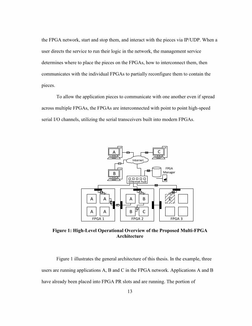
serial I/O channels, utilizing the serial transceivers built into modern FPGAs.
A A
AA
FPGA 1
A B
CB
FPGA 2
C
FPGA 3
Ethernet hub
A
Internet
B
C
FPGA Manager
Figure 1: High-Level Operational Overview of the Proposed Multi-FPGA
Architecture
Figure 1 illustrates the general architecture of this thesis. In the example, three
users are running applications A, B and C in the FPGA network. Applications A and B
have already been placed into FPGA PR slots and are running. The portion of

14
application A which is running on the PC is sending UDP packets to one of its pieces
running on the FPGA. That piece in turn is communicating with one of the other pieces
of A located on a different FPGA via a direct serial link between FPGAs. The same
situation exists with application B, except the other FPGA piece is located on the same
FPGA. This fact is transparent to the application pieces. Finally, the user's PC
application for C is directing the FPGA network manager to start the FPGA pieces of C.
The manager is partially reconfiguring FPGA 3 to contain one of the pieces of C.
3.1 Supporting Infrastructure
For each PR slot, instantiations of PR slot wrapper logic modules allow
applications hosted in the PR slots to communicate with other pieces and over the
Internet by managing the flow of data in and out of the slots. For inter-piece
communication, the wrapper handles constructing the proper route for the destination
before transmission. For Internet communication, the wrapper contains logic for
constructing headers around the data suitable for Internet transmission, as well as
verification of incoming data. For both types of communications, the wrapper handles
buffering of received and transmitted data to ensure good performance.
For inter-piece communications, a switch connects each PR slot wrapper and the
serial links together, providing the pathway for data to move between pieces on a single
FPGA as well as off-chip through the serial links. Data destined for off-chip is
moderated by frontend modules which sit between the switch and the serial links and
provide conversion between packet-based data and the streaming interfaces exposed by
serial channels. Data from the Ethernet interfaces is not routed between FPGAs by the

15
framework, however, there is still only a single Ethernet frontend module and multiple
PR slots, so a mux and arbiter provides the data pathway between a PR slot wrapper and
the Ethernet frontend. This module handles initial processing of packets received from
the Internet to send them to the correct application piece’s PR slot wrapper.
A partial reconfiguration engine receives data from the Ethernet interface and
provides the means by which the FPGA is reconfigured in the network. This engine
takes packets of data it receives from the management service described below and
funnels them into the Internal Configuration Access Port (ICAP), reconfiguring the PR
regions of the FPGA with new bitstream data. The engine employs a two-phase arm/fire
protocol to ensure that even if packets are lost or duplicated, an uninterrupted contiguous
bitstream is written to the ICAP. It also manages placing PR regions into a safe state
before reconfiguration, so that errant packets from the network will not arrive at an
application while it is partially configured. It is implemented as a special case
application piece which isn’t reconfigurable, and it is connected to the Internet via a PR
slot wrapper just like user application pieces. Finally, the management service
component is implemented as a Web server running on a PC. It provides a web-based
user interface to clients, allowing them to upload their application pieces, start and stop
their applications, and obtain information about how to communicate with them via the
Internet. This manager performs placement and routing of the application pieces in the
FPGA network, and communicates with the PR engine on each FPGA to install and
remove application pieces.

16
4. DESIGN
This section of the thesis discusses the design process which led to the framework
summarized above. The design tradeoffs involved in each component are analyzed, and
justification of the chosen implementation is discussed. Exact details are left to the
implementation section.
4.1 FPGA Application Interface
The design discussion begins by investigating the interface the framework
presents to user logic running on an FPGA in the network in order to allow it to
exchange data. The framework needs to provide a fixed interface of some sort in order to
allow different applications to be partially reconfigured into the same area on the FPGA.
The primary goal of this interface is supporting logic which consumes chunks of
data from a main application via the Internet, transforms it in some way (potentially by
interacting with other pieces on the FPGA network), and then transfers that data back to
that main application for further processing. The initial design assumes that these
application pieces do not require communications with off-chip peripherals or otherwise
require access to the I/O pins of the FPGA. Rather, of primary importance is the ease
with which data can be transferred between the main application and the FPGA pieces,
and between application pieces on the FPGAs. Design goals of this data transfer
interface are for it to be easy to use, high bandwidth, and as low latency as practical.
Applications should not need to know or write complicated logic to configure routing
between pieces on different FPGAs; that should be transparent. A piece should simply

17
be able to write bytes into an interface and have them appear on the other end regardless
of the location.
An application’s pieces may need to communicate with multiple other pieces, as
well as several different hosts on the Internet. One way to provide this capability to the
piece would be to offer a single port through which all I/O flows, with the application
piece addressing each destination regardless of whether it is a host on the Internet or
another piece on the FPGA grid. Combining the inter-piece and Internet communications
into a single port has the advantage of reducing the number of signals comprising the
partial reconfiguration boundary, and that can be important in successful place-and-route
timing closure. On the other hand, it potentially limits bandwidth as all communications
flows through that single port, and requires the application piece to multiplex data from
different parts of the piece into that port.
Instead, this design provides two ports to the pieces. Two ports, so long as they
are full-duplex, allow a piece to accept data from the Internet through one port,
transform it, and send it out to another piece via the other port for further processing
simultaneously without requiring user logic to do multiplexing or buffering of the data
while waiting for a single port to become available.
The primary benefit of using two ports, however, is that it allows the application
pieces to use different addressing schemes for data sent to the Internet versus between
pieces. As part of making the interface easy for application authors, one design goal is to
make it such that the pieces do not have to dynamically update destination addresses of
hosts on the Internet or other pieces at runtime. They can hard-code the address of the

18
other pieces into their logic and the application functions correctly regardless of where
the framework puts the pieces. The framework achieve this by allowing the application
author to choose the IDs each piece uses to communicate with other pieces statically at
application upload time, and the framework will use these IDs for routing between
pieces.
Data from the Internet will likely arrive from IP addresses that are not known at
the point the logic is synthesized, so users may still have to dynamically store the IP
address of hosts in their pieces. However, we expect that in the common case, a piece
receives data from a host on the Internet, processes it (potentially with help of other
pieces), then sends the result back to the same host. To make that workflow possible
without the application needing to store the host’s IP address, while still providing the
flexibility for the application to send packets to arbitrary IP addresses if it needs to, as
part of the port we provide signals containing the IP address and UDP port of the
incoming packet, as well as require the application piece specify the outgoing IP address
and UDP port. This setup means that if a piece wishes to send packets as replies to the
sender, it can connect the incoming signals to the outgoing signals in loopback without
any additional work.
Another design decision is how reliable to make the interface presented to the
pieces. Some applications will require a reliable transport, ensuring data arrives without
error and in-order. If the framework does not provide this functionality, they will need to
build it into their pieces’ logic. On the other hand, this framework uses UDP for Internet-
based communications, and the Xilinx Aurora library for inter-FPGA communications.
19
Both of these technologies are unreliable without additional layers on top of them, and it
would be simplest and use the least logic to simply carry that unreliable abstraction as it
is to the application pieces, letting them build in reliability if they need it. This also has
the advantage of logic savings for applications that can tolerate occasional data loss
(real-time media processing applications, for example). This is the approach taken in this
framework.
Finally, there is the question of what type of data transfer interface the
framework should use in communicating with the application pieces. In FPGAs today,
I/O between modules typically occurs in the form of FIFOs, RAMs, or busses. On Xilinx
FPGAs, the LocalLink FIFO port has traditionally been used for many of Xilinx’s IP
cores, including the Ethernet MAC and Aurora serial protocols used in this design [19,
20]. Distributed and BlockRAMs naturally use a RAM port, while ARM’s AXI standard
is popular when a bus is required. Orthogonal to these types of interfaces, data transfer is
either stream based, with no enforced delineation between sequences bytes, or packet
based with start/stop framing provided and enforced by the framework.
Both the Ethernet MAC and Aurora libraries used for final handoff of data off-
chip use LocalLink. The framework could do the same, and delineate packets with start
and stop tokens. There is a limited number of serial and Ethernet links and multiple PR
slots, so some form of arbitration is needed to moderate piece access to these links.
Presenting a LocalLink interface to the pieces and connecting the exclusively to the links
would be one way to solve the arbitration problem. Off-chip links would stream data
directly into the application pieces. When the piece finished sending or reserving data, it
20
would release the link for use by other pieces, effectively performing circuit-switched
routing internal to the FPGA.
However, we predict that application pieces will need the flexibility of random
access to the data. If we present the data as a stream, the pieces will have to buffer it into
a RAM internally. If we think most applications are going to need this, it makes sense to
pull that complexity into the framework instead of making every application implement
it. Furthermore, if applications do want to consume the data as a stream, they can very
easily do so by feeding the address line with a counter. One example of an application
which is easier to write when there is a random access interface to the data is the
framework's own packet verification module, which jumps around the data in a packet to
read information about the various layers of the IP+UDP packet. Additionally, if the
application pieces process data slower than the data arrives from the Ethernet or serial
links, connecting the link to the pieces directly prevents the links from receiving data for
other pieces while the first piece processes the data. Storing the packets of data in RAMs
temporarily solves the problem by handing one RAM off to the first piece while the link
stores further data in another RAM. Finally, Ethernet forces the data to be delineated
into packets anyway, and we predict that these packets will be a good size for many
applications to use as units of work.
The downside to the framework buffering the packet into a RAM before
presenting it to the application is that applications are always paying the cost of latency
for the framework to buffer the entire packet before presenting it to them. Despite this,
one advantage is that the framework can perform the verification of the packet's integrity

21
in parallel such that applications which don't care or can checkpoint their state can start
using the packet immediately, as described in the Ethernet Network Stack section. For
all the above reasons, the framework presents a RAM port to the application pieces for
them to exchange data with other pieces and with hosts over the Internet.
In summary, therefore, linking one piece to another is a receive/transmit pair of
byte-wide RAM ports, along with an ID signal to specify the destination piece. The
framework automatically routes packets sent from this port to the correct destination
piece, including any link multiplexing, in order and error-free. However, it performs no
error correction (packets with errors are discarded). The framework abstracts from the
application piece whether it is exchanging data with another piece on the same FPGA or
a different one.
Additionally, each piece wrapper contains a pair of byte-wide RAM port for
exchanging data over the Internet. The data presented to this port is encapsulated as UDP
Ethernet packets of up to 1500 bytes in length. Packet data is automatically routed to the
appropriate destination externally and incoming data has its checksum verified, but
otherwise no guarantees of ordering or reliable delivery are made. In both the piece-to-
piece and Ethernet ports, partial flow control is provided in terms of backpressure
ready/go signals pairs within a given FPGA. However, no flow control is provided
across Ethernet links or serial links between FPGAs. A small FIFO buffers packets
received by the framework and waiting to be acknowledged by the application piece; if
the application cannot keep up with the rate of incoming data, the framework drops the
22
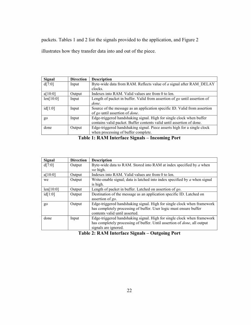
packets. Tables 1 and 2 list the signals provided to the application, and Figure 2
illustrates how they transfer data into and out of the piece.
Signal Direction Description
d[7:0] Input Byte-wide data from RAM. Reflects value of a signal after RAM_DELAY
clocks.
a[10:0] Output Indexes into RAM. Valid values are from 0 to len.
len[10:0] Input Length of packet in buffer. Valid from assertion of go until assertion of
done.
id[1:0] Input Source of the message as an application specific ID. Valid from assertion
of go until assertion of done.
go Input Edge-triggered handshaking signal. High for single clock when buffer
contains valid packet. Buffer contents valid until assertion of done.
done Output Edge-triggered handshaking signal. Piece asserts high for a single clock
when processing of buffer complete.
Table 1: RAM Interface Signals – Incoming Port
Signal Direction Description
d[7:0] Output Byte-wide data to RAM. Stored into RAM at index specified by a when
we high.
a[10:0] Output Indexes into RAM. Valid values are from 0 to len.
we Output Write-enable signal; data is latched into index specified by a when signal
is high.
len[10:0] Output Length of packet in buffer. Latched on assertion of go.
id[1:0] Output Destination of the message as an application specific ID. Latched on
assertion of go.
go Output Edge-triggered handshaking signal. High for single clock when framework
has completely processing of buffer. User logic must ensure buffer
contents valid until asserted.
done Input Edge-triggered handshaking signal. High for single clock when framework
has completely processing of buffer. Until assertion of done, all output
signals are ignored.
Table 2: RAM Interface Signals – Outgoing Port
23
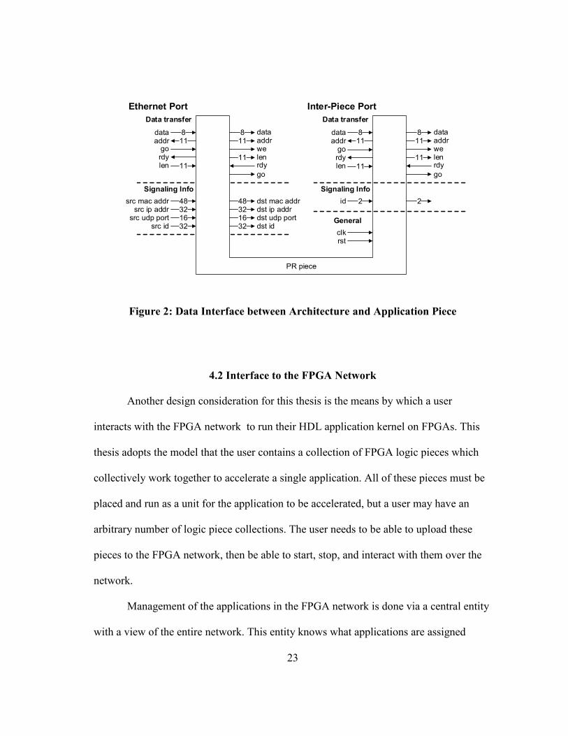
PR piece
Data transfer
811
dataaddr
rdylen
Signaling Info
48321632
src mac addrsrc ip addr
src udp portsrc id
811
11
dataaddrwelenrdy
go
48321632
dst mac addrdst ip addrdst udp portdst id
Ethernet Port
Data transfer
811
dataaddr
Signaling Info
2id
General
clkrst
811
11
dataaddrwelenrdy
go
2
Inter-Piece Port
go
11rdylen
go
11
Figure 2: Data Interface between Architecture and Application Piece
4.2 Interface to the FPGA Network
Another design consideration for this thesis is the means by which a user
interacts with the FPGA network to run their HDL application kernel on FPGAs. This
thesis adopts the model that the user contains a collection of FPGA logic pieces which
collectively work together to accelerate a single application. All of these pieces must be
placed and run as a unit for the application to be accelerated, but a user may have an
arbitrary number of logic piece collections. The user needs to be able to upload these
pieces to the FPGA network, then be able to start, stop, and interact with them over the
network.
Management of the applications in the FPGA network is done via a central entity
with a view of the entire network. This entity knows what applications are assigned

24
where and can manage placement globally as applications come and go. This
management entity runs on a PC; users interact with it as a web service using HTTP
calls. Users upload their application and a set of constraints about how their application
pieces communicate with one another. Once a user directs the framework to start the
application, the framework determines how to place the application pieces to best honor
the user’s constraints, then sends back to the user the IP addresses associated with the
pieces of their application. One key point to note here is that the management entity does
not moderate communication between the users in the Internet and the FPGAs
themselves; it only manages the placement of the pieces. Each FPGA contains enough of
a network stack to communication with the users directly over Ethernet, allowing the
network of FPGAs to scale without the management PC becoming the I/O bottleneck.
As part of uploading an application to the framework, the user describes how
many pieces an application contains and the connectivity required between these pieces
as a graph, with the pieces as nodes and the connections as edges. Even though the
framework provides the ability for pieces of an application to communicate with one
another, all pieces are not automatically connected to one another. Instead, the user
describes which pieces actually internetwork.
While any placement on the FPGA network where pieces can exchange data
fulfills the requirement described by the user, we can optimize the performance of
applications by more careful placement. We predict that among different applications,
and even within the pieces of a single application, certain pieces may need to exchange
large amounts of data, or do so with low and deterministic latency. Other pieces may not
25
care as much. For example, one piece may exchange compressed data with another
piece, which then uncompresses it before forwarding it on to other pieces. The links
between pieces handling uncompressed data will require more bandwidth than the link
with compressed data. It would be nice to use this information to inform our choice of
application piece placement.
Toward that end, we allow the user to specify, when the application is uploaded
to the FPGA, characteristics of the links between communicating pieces regarding their
bandwidth and latency needs. Initially, we will rely on applications being good citizens,
but in the future one could imagine incentivizing application authors to be honest by
charging a higher rate for applications with many low latency links or the like.
Currently, the framework provides only simple constraints for edges: each edge has a
bandwidth and latency requirement, and these are Boolean values. As an example, an
application could request one link between two pieces be a low latency, high bandwidth
link, while specifying that the remaining links can tolerate high latency, low bandwidth.
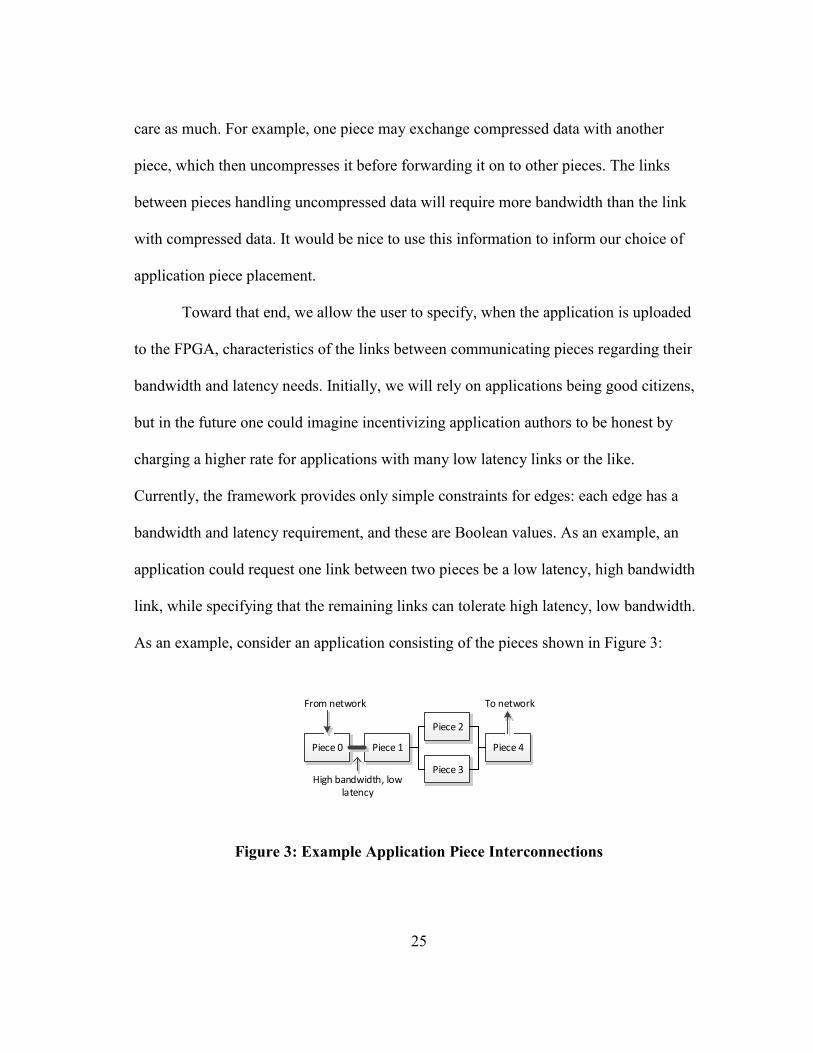
As an example, consider an application consisting of the pieces shown in Figure 3:
Piece 0 Piece 1
Piece 2
Piece 3
Piece 4
High bandwidth, low latency
From network To network
Figure 3: Example Application Piece Interconnections

26
Then, the management entity could place the application pieces on the FPGA
network as shown in Figure 4, ensuring high-bandwidth links are on the same FPGA,
while allowing pieces with non-critical links to be placed on different FPGAs:
FPGA #1
Piece 0 Piece 1
FPGA #2
Piece 2
Piece 4Piece 3
Our application
Other existing applications
Slower inter-FPGA links
Figure 4: Example Application Piece Physical Placement
4.3 Framework Data Transport Overview
Having defined the interface provided to the application pieces as well as concept
of pieces communicating over the Internet and with one another on different FPGAs, the
next portion of the design deals with questions surrounding how to adapt LocalLink
interfaces to RAMs, as well as how to arbitrate access among the multiple application
pieces’ access to the limited number of Ethernet and serial off-chip links. It also
discusses the related question of routing data. The first point of discussion is connecting
the application pieces to Ethernet (for Internet access) and GTP serial transceivers (for
inter-FPGA data transport). Both of these interfaces use LocalLink, a FIFO streaming
interface. Next, we address the question of data arriving from the Internet and
determining the correct application piece to receive that data. Similarly, when one

27
application piece wants to send data to another, how do we figure out where to send it?
What addressing scheme does one piece use to communicate with the other?
The way we solve LocalLink to RAM conversion is as soon as possible, data
from off-chip links is converted from LocalLink and placed in a RAM buffer, which is
henceforth used as the unit of data transfer internal to the framework. The modules
which convert to and from LocalLink are called off-chip frontends, accepting LocalLink
on one end and presenting a RAM port on the other. Each application piece is connected
to a piece wrapper, which hosts the RAMs used by the piece for sending and receiving
data. These piece wrappers abstract from the piece the details of getting the data to its
destination, sending and receiving data from other pieces, the inter-FPGA serial links, or
Ethernet as required. Arbitration is performed by a switch communicating with each off-
chip link and piece wrapper. The switch arbitrates access to the incoming RAM ports of
each of the wrappers and frontends.
Routing is different for the Ethernet network versus the inter-FPGA network. For
Ethernet, each PR slot is assigned an IP address, and as the frontends receives incoming
packets, it chooses a PR slot based on the IP address of the packet. For inter-FPGA links,
we wanted the applications to be able to communicate without worrying about exactly
where the other pieces were placed on the FPGA grid. Therefore, when uploading the
application, the user assigns an ID to each piece which the piece uses when sending data
on its inter-piece port. When placing the pieces, the framework calculates a source route
between each piece of the application and stores these routes in the piece wrappers. As a

28
buffer of data travels from wrapper to switch to frontends, each element removes an
address from the front of the packet and uses it as the next destination.
4.4 Off-Chip Communication Methods
This section examines the different possibilities for connecting FPGAs together
and to users of the framework. Interconnecting FPGAs is treated separately from
connecting the FPGAs to users. Users interact with the FPGAs using the standard
Ethernet/IP/UDP protocol stack, while inter-FPGA communications are shunted to
point-to-point serial links as an optimization.
4.4.1 Internet
For this architecture, we choose to connect the FPGAs to the users on the Internet
by connecting them directly to an Ethernet network and implementing a network stack in
FPGA logic. This is as opposed to connecting a subset of FPGAs to a PC using PCIe or
other local-PC communications protocols, then making the PC responsible for proxying
data to/from the Internet. This simplifies the design of our FPGA network, as we don’t
need to a pair a PC with every few FPGAs. Most FPGAs of sufficient size to be
interesting for use in accelerating algorithms contain hardware Ethernet MACs capable
of Gigabit Ethernet, and existing FPGA IP cores provide good support for low-level
Ethernet functionality. Gigabit Ethernet is ubiquitous, and fast enough to prevent the link
to users from being the bottleneck.
Using Ethernet as a communications transport for FPGA designs is not a new
idea; however, Ethernet alone has several problems which make it problematic as the
sole I/O pathway between users and the FPGAs. FPGA hardware handles sending raw

29
Ethernet data, but does not handle higher level protocols and routing. Raw Ethernet data
won’t route across the Internet, and would require a PC to relay the data for each FPGA.
That is the problem we are trying to avoid by connecting the FPGAs to Ethernet in the
first place. Therefore, on top of Ethernet, our design implements a minimal Internet
Protocol v4 and User Datagram Protocol (IP/UDP) stack in FPGA logic. IP is a
prerequisite for communicating over the Internet, while implementing support for UDP
allows users to communicate with the FPGAs using standard PC applications without
requiring them to install drivers or have administrative privileges to send and receive
other IP protocols. At the same time, UDP is still low-level enough to be simple to
implement in HDL (as opposed to TCP). It’s also flexible enough that applications can
implement additional functionality on top of it in their piece’s HDL, if required.
One problem with Ethernet is that unlike technologies designed for local-PC
communication such as USB or PCI Express, where the link is engineered to provide
such low error rates that for practical purposes errors may be ignored, Ethernet networks
are expected to occasionally encounter errors which must be handled reasonably. Errors
can occur in two forms. In the first case, packets can be lost in the network, such that
they never arrive at the FPGA or PC. The other is that data is occasionally corrupted. To
detect this situation, all three layers (Ethernet MAC, IP and UDP) provide checksums
protecting their header fields and data contents.
For incoming packets, the Ethernet network stack accepts Ethernet packets,
decodes them to determine if they contain IP/UDP frames destined for the FPGA, and
checks them for validity before delivering them to the application pieces. It also

30
constructs correct IP and UDP headers around outgoing buffers of data from application
pieces. Verifying and constructing correct checksums merits additional design
considerations because both operations require making a pass over the entire packet of
data, potentially a time consuming operation.
One simple approach would be to read the entire packet into a buffer first, then
verify the checksums. If there are no errors, deliver it to the application piece. This
requires reading the packet twice: first for computing the checksum, then by the
application piece for its purposes. Pipelining this packet verification prevents reducing
total framework throughput, but increases the latency before the application piece can
begin using the packet of data. However, since we are implementing the network stack
in HDL, we can take advantage of the dual port ability of on-chip BlockRAMs to verify
the packet concurrently with the application using it. Once a packet arrives the
framework assumes it’s valid and immediately hands it off to the application piece for
processing. In parallel it begins verifying the integrity of the packet; once finished, it
notifies the application piece about the packet's validity. In this way, application pieces
have a choice. They can wait for the packet to be verified, incurring latency. Or, if they
are stateless or have a means of check pointing and restoring their internal state, then can
start operating on the data immediately, reverting to the last checkpoint in the rare case
where the packet is corrupt. This later approach is what we use in this prototype.
The above discussion assumes that the entire packet must be streamed into a
RAM before the framework can validate the checksum. Future work could investigate
the possibility of verifying the checksums of the packet while it is being streamed into

31
the application piece’s RAM, such that the application knows the integrity of the packet
as soon as it is ready for processing. One potential downside of validating the packet
checksum in-line while streaming the packet data in from the Ethernet MAC is that the
checksum logic needs to be able to run as fast as the rate of incoming data. For Gigabit
Ethernet this isn’t a problem, but for faster line rates, our approach may have the
advantage of allowing many slow application + verification units to process the
incoming data stream in parallel.
Although the Ethernet framework detects corrupt packets and informs the
applications of this fact, as a consequence of choosing UDP it is up to the applications to
detect lost packets if it is important to them. Due to the large bandwidth delay product at
gigabit rates, stop and wait error ARQ will be insufficient for most applications where
data loss is important, and they will need to implement some form of error detection
utilizing sequence numbers. To support those applications, the framework adds an
additional pseudo-protocol on top of UDP in the form of a 4-byte sequence number
which the framework automatically removes prior to passing the data onto the
application piece. This number is made available as a separate signal to the application
without it needing to extract the bytes from the incoming packet manually.
The logic required to verify the checksum of the Ethernet, IP, and UDP protocols
is called the packet verification unit. For this design, we pair one verification unit with
each PR slot. Paring a verification unit with a PR slot tightly couples them together,
simplifying the control logic. A unit never verifies packets for more than a single app
piece, and its paired app piece need look at only a single unit for validity information

32
regarding the packet it is processing. Paring a verification unit with a PR slot also fits
well with realistic physical limitations of FPGAs. In particular, both the unit and app
piece are implemented on the same FPGA, in close proximity to one another. It is
therefore a reasonable first approximation to assume that as Ethernet line rates scale
higher, both the unit and piece will experience similar limitations on clock speed and
will be able to process incoming packets at about the same rate. (If the common usage
pattern turns out to be application pieces which perform significant amounts of
computation and process a relatively small bandwidth of network traffic, as future work
it may make sense to re-visit this decision decouple the packet verification units such
that a smaller number of them handles verification for multiple PR slots.)
4.4.2 Locally
With the framework providing the ability for applications, divided into logical
pieces, to communicate with one another through RAM-based ports, one important
design question is how to move data between pieces when they are located on different
FPGAs. We would like the method chosen to be high bandwidth, ideally allowing pieces
to exchange data as fast as they can send it out the port of their piece interface, and with
as little latency as possible between sending and receiving a message.
Before delving into possible designs, it's worth considering what the application
experience would be like if we do nothing. If an application was too big to fit on one
FPGA, software running on the user’s PC would be responsible for capturing the data
from one piece and presenting it to others. Aside from the complexity imposed on the
users with this approach, we expect the bandwidth from the user’s PC to the FPGA

33
network to be a limited subset of that available from inter-FPGA serial links.
Alternately, we could still use the existing Ethernet link designed for communicating
with users, but build facilities into the framework to allow inter-piece communication
without the user manually transferring the data over the Internet. This would ease the
task of the application author from having to manually transfer data to a PC over the
Internet and back again, probably improving bandwidth limitations. However, it would
send inter-FPGA traffic through the same single Gigabit Ethernet link also carrying data
back to the user’s PCs. Of course, we could improve this situation by utilizing additional
Ethernet links for handling inter-FPGA traffic. However, then we would run into the
problem that most FPGAs have a limited number of Ethernet MACs. Furthermore, using
Ethernet forces whatever interface we present to the applications for inter-FPGA data
transfer to be packet-based due to the design of Ethernet, as well as carry a fixed
overhead in the form of the Ethernet header for each packet sent. Finally, most Ethernet
switches employ a store-and-forward approach to relaying messages, increasing latency
for these data transfers.
On the other hand, FPGAs typically do contain a large number of high-speed
serial transceivers on the silicon. These transceivers are capable of transporting data
faster than Gigabit Ethernet, and the quantity available on most FPGAs opens up
interesting topological structures for inter-connecting FPGAs by utilizing more than one
physical link. This can increase inter-piece bandwidth and reduce congestion. For those
reasons, this design uses high-speed serial transceivers to link FPGAs together over a
separate network from the Ethernet link, and uses this second network to carry inter-
34
piece traffic between FPGAs. These serial transceivers provide a low level interface
analogous to that of an Ethernet PHY, and used directly require the consumer to deal
with clock drift between boards and as a consequence the need to provide flow control or
deal with occasional data loss, as well as framing to distinguish one message from
another. A plethora of protocols of varying complexity and hardware logic implementing
those protocol exist to make these serial transceivers easier to use. For this
implementation we chose to use Aurora, which is a protocol and IP core developed by
Xilinx which handles clock skew and framing, and presents a LocalLink interface for
sending and receiving data. For more information about high-speed serial links, see
Appendix A.
4.5 Data Movement between Pieces and Off-Chip Links
4.5.1 Connecting Pieces and Off-Chip Links
In order to allow multiple pieces and off-chip links to communicate with one
another, some form of arbitration is needed to moderate access to the receive ports of
each of these entities. With the Ethernet network, the design is simpler because there is
only a single off-chip link and we have made the decision that pieces may only
communicate with hosts on the Internet over this link, not with one another. Therefore,
the only contention is when multiple pieces try to send packets at the same time. We can
handle that case with a single 1 to N arbiter. For the piece-to-piece network, things are
more complicated because any piece or off-chip link can want to send data to any other
piece or off-chip link at the same time. Additionally, unless we implement a fully-
connected graph of links connecting the FPGAs to one another, we must decide whether

35
to allow communications only between pieces on adjacent FPGAs connected directly to
one another via a serial link, or whether to allow piece’s data to route through one or
more intermediate FPGAs. Restricting communications to adjacent FPGAs is simpler,
but breaks the abstraction of the applications not having to care about the physical layout
of their pieces, which we felt was unacceptable.
One possibility for arbitration is to use a stream-based protocol for connecting
pieces and links together, then allow sending pieces to request exclusive access to their
destination for as long as they have data to send. This approach fits nicely with the
LocalLink interface used for the Ethernet and serial IP cores. This effectively circuit-
switched routing approach to arbitration is also nice in that it allows low jitter between
entities once the connection is granted, but is more complicated to implement across
multiple FPGAs than a packet switched system, and makes it hard to ensure fairness
between multiple pieces and links unless some means is provided of revoking access to
the sender after some timeout. However, having a timeout somewhat diminishes the
advantage of exclusive access in the first place. The potential fairness problems are
magnified if the circuit is established across multiple FPGAs (a requirement if pieces are
allowed to be placed anywhere in the FPGA network and the network is not fully
connected), as a single channel between two pieces can hold-up the serial links spanning
multiple FPGAs. In practice, as the network grows, the FPGA chips will not have
enough serial interfaces to implement a fully connected network, and we shouldn’t rely
on this requirement as we design the framework.
36
Instead, we could create a packet switched system, choosing at the receiving
FPGA of each serial link where to send the packet next. This avoids the complexity of
reserving a circuit across multiple FPGAs, and by limiting the message size of the
packets, allows the framework to deal with fairness issues by employing scheduling
algorithms on the sending side FPGA of each serial link (for example, round-robining
each piece’s packets). For this framework we chose this approach, and transfer data
between pieces, whether locally or on different FPGAs, as packets.
4.5.2 Data Buffering
Having made the decision to use a packet switched system to arbitrate the flow of
data between pieces and off-chip links, we need some mechanism for storing the packets
of data as they move through the framework, because our application interface specifies
that pieces have random access to incoming data as if it were in a RAM. For this data
storage, the framework uses FPGA-internal RAMs, called BlockRAMs on the Xilinx
chips used for our prototype, for buffers as the data flows through the framework. They
are 18 kilobits large and can be partitioned in a variety of data widths and depths. One
supported configuration, 9 bits wide and 2,000 elements deep, is well suited for Ethernet
frames, which normally consist of up to 1500 bytes of data.
We considered other ways of storing the data, including Distributed RAM (RAM
implemented using FPGA logic cells) as well as off-chip SRAM or DRAM. However,
using Block RAM as opposed to Distributed RAM conserves logic fabric for application
access. External DRAM or SRAM would require designing a memory controller to
arbitrate access to multiple application pieces simultaneously, and such complexity was

37
beyond the scope of this prototype. Utilizing Block RAMs does have the disadvantage of
making timing more challenging, as the place and route algorithm is not always able to
locate the Block RAM and the logic using it physically close to one another on the
FPGA. The Ethernet MAC and Aurora serial modules send and receive data through a
LocalLink FIFO, which streams data sequentially. Since these modules do not access
data randomly, we can add pipeline stages between these module and the RAMs as
needed to meet timing without incurring performance issues. Because of this sequential
access, it is not important that we locate the RAMs near to these modules. On the other
hand, we want to provide random access to the data for the application pieces. The closer
we can place the RAMS to the PR slots, the fewer cycles of delay the pieces will
experience between presenting an address and receiving the data from the RAMs.
Block RAMs have the ability to be configured as true dual-port RAMs, which
means they can be simultaneously read and written to by two different elements in the
design. Therefore, the simplest architecture for moving data from the off-chip links to
application pieces is to utilize a single RAM with one port connected to the off-chip link
and the other port connected via a multiplexor (mux) to the destination application piece.
Since only a single piece can be consuming data at any given time (because there is only
a single RAM) the mux would be controlled by a chip-select line indicating which piece
is active. This approach, while simple, is inadequate as incoming data cannot be received
concurrently with an application processing data, and the design can never achieved
100% utilization of the off-chip link.

38
Adding sufficient BlockRAMs for buffering more packets can alleviate the
utilization issues of the off-chip links. However, allowing the off-chip links to connect to
any RAM requires a wide mux, which has the disadvantage of requiring a large amount
of FPGA logic and routing resources. On the other end of the buffer, each application
piece needs to be able to connect to whichever buffer contains its next piece of data,
requiring more wide muxes. Worse, allowing any application piece to connect to any
RAM means that at least some of the pieces will have poor spatial locality with a RAM
they need to use, decimating the possible clock speed of the design unless pipeline stages
are inserted.
Since routing constraints effectively partition the location of RAMs such that
only a subset can be used by an application piece without inserting pipeline stages to
meet timing closure, it makes sense to design for these constraints. A subset of RAMs
and an application piece become logically grouped together, and the RAMs are
considered to belong to the piece. Instead of a wide mux connecting the incoming off-
chip link to all the RAMs, and additional wide muxes connecting the RAMs to all the
pieces, we break up the muxes. Connecting the Ethernet interface is a two-level mux
structure. Then, a single mux connects the RAMs to the pieces, as illustrated in Figure #
below.
For this initial implementation, this design allocates two RAMs for each
application piece. This is sufficient for the application to achieve 100% utilization of the
port so long as it processes packets at least as fast as they arrive. Figure 5 illustrates how

39
the framework connects these two RAMs with muxes to the application logic and the
rest of the framework:
Figure 5: Partitioned Multiple RAM Design with 2 Level Data Source MUX
Because of all the advantages just described, the partitioned multiple RAM
buffer approach is what we use for the internal routing of off-chip link packets to pieces.
4.5.3 Switching
At this point we have discussed the rationale for choosing a packet switched
system for moving data between application pieces and off-chip links, then elaborated on
the system of BlockRAM memories used to store those packets. Here, we discuss the
design of the switching infrastructure used to connect the piece and off-chip links’ RAM
ports together appropriately.
The design for receiving data from off-chip links as described thus far can be
broken down into 5 modules. A frontend module receives data from off-chip, providing
an adapter between LocalLink used by the IP core and the RAM ports used by the rest of
Data
Source
(Ethernet
MAC)
Data Sink
(Application
Tile)
RAM
RAM
MUX
MUX
Data Sink
(Application
Tile)
RAM
RAM
MUX
MUX
MUX

40
the framework. Then, a switch routes the data from the frontend to the appropriate
piece’s RAMs based on some routing field in the packet. For Ethernet, this is the
packet’s destination IP address, and for serial it is the next hop in the source route. Third,
a second level mux/RAM stage buffers packets waiting to be processed by the piece. A
PR slot wrapper module contains this second level mux/RAM for a PR slot, and for
Ethernet, the packet verification module. When the application piece is ready, the PR
slot wrapper connects the appropriate buffer to the piece for processing. This design is
duplicated twice; once for the Ethernet network, and once for the inter-FPGA serial
network.
There is only a single Ethernet link, and application pieces cannot send data from
one piece to another over this network. Therefore, a simple 1-N mux is sufficient for
routing incoming Ethernet data to pieces. However, the Ethernet's outgoing port, and
every piece's incoming port are potentially contended by multiple senders at once. For
Ethernet, all pieces are sending to the same Ethernet frontend, and a single arbiter in the
frontend can manage access to the pieces. The piece-to-piece network is similar to the
outgoing path of the Ethernet network but in both directions, now there are multiple off-
chip serial links, and every piece and link can send data to each other. (Data received
from links can not only be delivered to application pieces, but also to other links, so that
inter-piece data can be routed through intermediate FPGAs.) Every application piece’s
incoming port is potentially contended by multiple senders at once. The 1-N first level
mux is no longer sufficient.

41
There are several different approaches we could take for connecting the
application pieces and serial links. An internal shared bus connecting all the endpoints
together is one simple option, and it avoids the complexity of building muxes. However,
multi-drop input/output signals in FPGAs tend to be slow and limit overall system
timing. Busses also have the problem of shared bandwidth unless the bus runs faster than
the piece and serial link ports (which is unlikely, given the aforementioned problem of
multi-drop signals on FPGAs) or is very wide. If it runs faster or slower, there’s also the
issue of crossing clock domains to move data to and from the bus.
Alternately, we could interconnect the pieces and links by creating a fully
connected N-N switch such that every piece and serial link’s incoming port is moderated
by a 1-N mux and arbiter. This approach has advantages of being simple to design
compared to a crossbar switch, as well as never blocking communications between
pieces or links due to limitations of the routing architecture. However; it suffers from the
problem experienced by all fully-connected networks: the number of edges grows
exponentially with the number of nodes. For large numbers of serial links or application
pieces, this can quickly overwhelm the routing resources of the FPGA.
To mitigate the exponential wiring growth, a crossbar switch could be used
instead of a fully-connected one. This comes at the cost of some blocking probability, as
well as increased implementation complexity. Alternately, a Network on Chip could be
used, with pieces and links connected to routers, and the routers linked together. This
doesn’t really mitigate the problem of wiring explosion; it just controls it by adding a
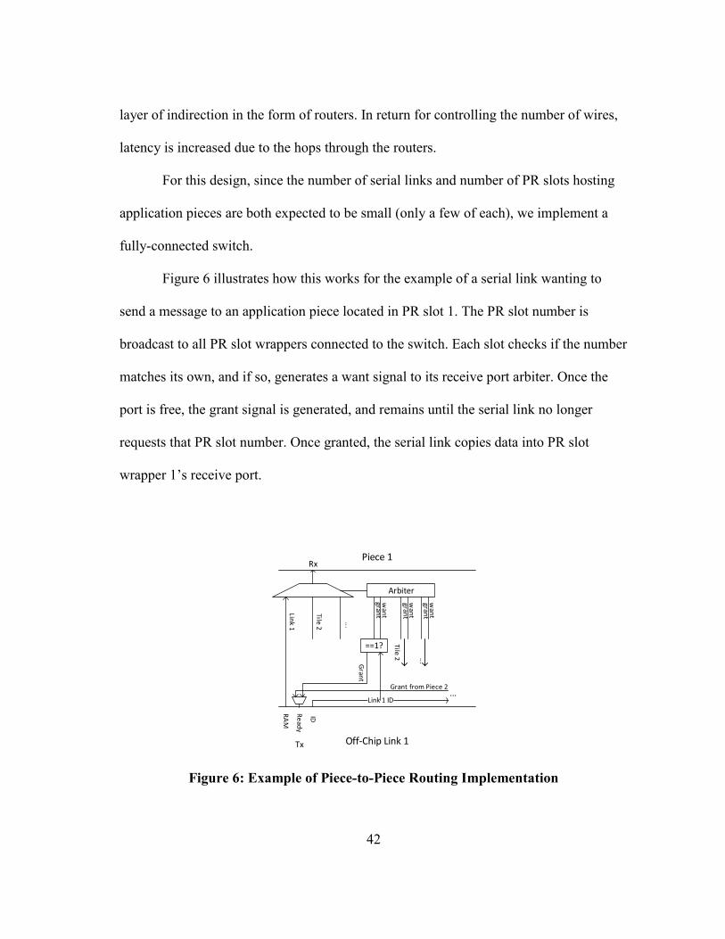
42
layer of indirection in the form of routers. In return for controlling the number of wires,
latency is increased due to the hops through the routers.
For this design, since the number of serial links and number of PR slots hosting
application pieces are both expected to be small (only a few of each), we implement a
fully-connected switch.
Figure 6 illustrates how this works for the example of a serial link wanting to
send a message to an application piece located in PR slot 1. The PR slot number is
broadcast to all PR slot wrappers connected to the switch. Each slot checks if the number
matches its own, and if so, generates a want signal to its receive port arbiter. Once the
port is free, the grant signal is generated, and remains until the serial link no longer
requests that PR slot number. Once granted, the serial link copies data into PR slot
wrapper 1’s receive port.
Link 1
Tile 2
Arbiter
wan
tgran
t
wan
tgran
t...
wan
tgran
tTile 2
Rx
...
Off-Chip Link 1
==1?
Gran
t
Re
ady
ID
RA
M
Tx
Piece 1
...Grant from Piece 2
Figure 6: Example of Piece-to-Piece Routing Implementation

43
4.6 Routing Incoming Ethernet Packets to Pieces
In our architecture, the purpose of the Ethernet interface is for data transport
between application pieces on the FPGA to the user’s PC applications. Because the
framework is never acting as an intermediate router for Ethernet packets destined to
another FPGA, routing packets from the Ethernet network is relatively simple because
all packets either originate from or are destined for the local FPGA. The framework
really only has one routing task: when an incoming packet is received, determine which
application piece receives the data.
One option for achieving this routing would be to broadcast the first portion of
the packet to all PR slots and let the application pieces choose whether to accept the
data. In addition to requiring an arbiter if multiple pieces claim the packet, this also
pushes complexity to the application pieces. However, such an approach could be a
simple way to load balance data among identical application pieces without the
application on either the PC or FPGA framework needing to manage it.
The other option is to have the framework route packets and deliver them to the
appropriate application piece itself, based on some routing field. One option would be to
use a range of bytes from the packet payload as the routing field. Although protocol
agnostic, it requires that the framework parse extra information to make its routing
decision, and requires cooperation from the application running on the user’s PC to
insert this routing information. Another approach is to utilize the fact that these packets
will be Ethernet + IP + UDP. Each of these protocol layers carries information that can
be used to route packets. Furthermore, the communications architecture must already
44
read these headers in the process of verifying the packet integrity. Ethernet MAC
addresses are not globally routable on the Internet. Both IP addresses and UDP ports,
however, are good candidates for a routing field, as both are easily set from a PC based
application using the standard Berkley sockets API. Of the two, using IP addresses has
the advantage of leaving the entire UDP header untouched for potential application
usage, so that is what we use for this thesis: each PR slot is assigned a unique IP address,
and only packets with the PR slot’s destination IP address are forwarded to the slot.
The RAM port provided to the application piece is offset to index into the data
payload of the UDP packet past the 4 byte sequence number. Then, as part of application
piece’s Ethernet port, we pass the source and destination IP addresses, UDP source and
destination ports, and the sequence number as signals. In what we expect to be the
common case where an application piece accepts data from Internet, performs
processing, then returns the result back, the piece can simply connect the source and
destination IP and sequence number signals together internally and allow the framework
to handle all details of routing the data correctly with the correct sequence number, while
still retaining the flexibility to send to other destinations if needed.
4.7 Off-Chip Piece-to-Piece Routing
Another important design question is how we multiplex packets from multiple
application pieces onto a single serial link between FPGAs. As discussed previously, it
would be simplest to require that application pieces which wish to communicate with
one another be located in one specific PR slot on each FPGA which is connected to the
serial link. However, one of the goals of this framework is to abstract the limits of a

45
single FPGA from the application. Pieces should be able to communicate with one
another regardless of their location in the FPGA network, and their physical location
should be transparent to the pieces.
As described in the application piece interface section, we want to allow
application pieces to communicate with one another by an addressing scheme
independent of the actual location of the pieces on the FPGAs. This address goes from 0
up to the number of other pieces a piece communicates with, as specified in the
application configuration provided when the user uploads the application. As described
in the Piece to Piece Mux section, pieces and serial interfaces are connected to one
another through a fully-connected switch. If pieces were only communicating with other
pieces on the same FPGA, we wouldn’t really need any routing; each PR slot wrapper
would just present an address to the switch to send data to the correct destination
application piece, and it could do this by keeping a mapping between the application’s
virtual address for the piece and the corresponding input into the switch required to
reach that piece.
Things are more complicated, however, when pieces are allowed to communicate
across FPGAs. In addition to feeding the switch the right signal to send packets to one of
the serial interfaces, the PR slot wrapper also needs a way of telling the serial frontend
on the other FPGA what to do with the packet from there (in other words, what address
to feed its switch when receiving the incoming packet.)
The way we solve this in this framework is by using a simple form of variable-
length source routing. Once the pieces of an application have been placed onto the

46
FPGA network and the application started, they are fixed for the lifetime of the
application. Furthermore, connections between application pieces are specified as part of
the application configuration and are also static. Because pieces of an application are
placed by a central entity with fully knowledge of the entire network, it’s possible to
determine all the routes between the pieces up front.
Each PR slot wrapper contains all the routing information needed to reach every
other PR slot holding that application’s pieces. After placing application pieces, for each
piece the framework calculates the route to each other reachable application piece using
source routing. These source routes are then programmed into the wrapper, which keeps
these routes as a mapping of application specific destination IDs to the source route
required to reach them. This route is variable length depending on how far away the
destination piece is (on the same FPGA or multiple FPGAs away). When the packet is
transmitted, if the packet’s destination is a piece on another FPGA, the wrapper appends
this variable length route to the beginning of the contents of the outgoing packet before
forwarding it to one of the serial links. As the packet of information flows from one link
to the next the first address in the source route identifies the next destination. This has
the advantage that the framework, including the serial links and FPGAs which are only
relaying packets, do not need to have any intelligence in determining where to send the
packet next: they simply examine the next hop in the source route. Before passing the
packet along, each serial frontend module removes one address from the front of the
route such that by the time it reaches the destination only the message remains. The last

47
entry in the source route is not an address for routing the packet, but indicates the source
piece which sent the packet, so that the receiver knows the address of the sender.
Figure 7 illustrates an example topology, followed by the source route generated
by the framework for this topology:
PR Slot 0 (Source) -> Off-Chip Link 1 (Hop 0) -> Hop 1 -> PR Slot 3 (Destination)
Slot 0 Slot 1
Slot 3Slot 2
Mux
Off-Chip
1
Off-Chip
0
Slot 0 Slot 1
Slot 3Slot 2
Mux
Off-Chip
1
Off-Chip
0
Slot 0 Slot 1
Slot 3Slot 2
Mux
Off-Chip
1
Off-Chip
0
[ Hop 1 ] [ Dest ] [ Src ASID ] [ Data buffer contents ]
[ 0 ] [ 4 ] [ 0 ]
Figure 7: Routing Application Data through Intermediate FPGA
The routing code is prepended to the data buffer upon transmission. Hop 0 is
directly specified by the source piece’s PR slot wrapper, as it directly controls the local
FPGA's switch, directing the packet to Serial Link 1 link. Hop 1 and destination are IDs
of the PR slot wrappers and serial link frontends in the framework used as input to the
switch on each subsequent FPGA. Upon receiving a message, each serial link frontend
removes the first byte of data from an incoming LocalLink frame and presents it to the
piece-to-piece switch as the destination ID. When the switch is ready, it then copies the
LocalLink stream into a RAM, similar to the Ethernet frontend module. In this way, as
the message travels from one FPGA to another, the serial link frontends peel the source

48
routing addressing information on each hop, until when the message arrives at the
destination, only the source ID remains.
In the case of a message which remains inside the domain of a single FPGA and
is sent directly from one piece to another, the packet contains only the source ID, as
there is no inter-FPGA communication and therefore no need to encode any source
routing information inband.
Such an approach does have the disadvantage that the route is static and cannot
dynamically change to accommodate traffic between links or if a link fails. In practice,
link bandwidth is not infinite, and the best route in terms of bandwidth and latency
available to the endpoints may change dynamically depending on the link utilizations.
However, dynamically updating the routes in response to changing traffic conditions is
left as a future work.
4.8 Application Piece Placement and Configuration
4.8.1 Placement Algorithm
By sub-diving the FPGA into smaller PR regions, and providing a way for
application pieces in those regions to communication between each other, we face a
place and route problem in determining where to place application pieces such that they
are as close to each other as possible. Especially important is that pieces which the user
has indicated require high bandwidth communication between one another are situated
so to make that possible. This situation is not unlike that faced by the FPGA tools when
placing and routing LUTs onto FPGA fabric. In our framework as in FPGA tools, the
challenge is to determine interconnect and placement of our nodes well enough that the

49
constraints on their edges are honored acceptably, while avoiding the inconvenient fact
that optimal placement is NP-complete.
From a correctness point of view, so long as application pieces which have an
edge between them are able to exchange data with one another, pieces may be placed
anywhere there exists space for them on the FPGA grid. Our framework has an
advantage that poor routing only affects performance; not correctness. Edge constraints
supplied by the user when uploading the application are only hints to the framework on
which the application must not rely. There is more bandwidth between pieces on the
same FPGA than there is between pieces on separate FPGAs, due to the need to
potentially share serial links with other applications. Additionally, in realistic
configurations of this architecture, the FPGAs will not be interconnected to one another
with a complete graph of serial links. Therefore, some placements of application pieces
will require the piece data to route through intermediate FPGAs to reach its destination
piece. We would like to avoid that situation if possible, as it increases contention on the
intermediate FPGAs serial links.
Therefore, the lowest latency and highest bandwidth occur when two pieces are
placed on the same FPGA. In that case, each piece gets its own dedicated channel
between each other, with the only sharing occurring if a piece communicates with
several other pieces and has to share its outgoing interface. If that is not available, the
second best option is on different FPGAs which are as close to each other as possible;
that is, they route through few other FPGAs. The situation becomes more complicated if
we take the congestion of the links between the FPGAs into account. The optimal route

50
can change dynamically depending on the other traffic on the FPGA network, and we
would need a way to update the routing between pieces dynamically at runtime as the
situation changes. On the other hand, if we consider only each pair of pieces in isolation
and assume all links are unloaded, we can determine the good locations to place an
application once when the application is uploaded. This is what we do for the initial
implementation.
Our placement algorithm operates statically, when a user requests the framework
start an application. It operates in two stages. First, it looks through the application
description to determine which pieces communicate with one another, and which of
those links require high-bandwidth or low-latency. It groups the pieces which
communicate with each other via these links into clusters, and attempts to place the
clusters first. Attempting to place variable length low-latency clusters of application
pieces on the FPGA network constitutes a bin packing problem. If possible, we want to
fit each cluster completely on an FPGA, and for that we employ a best fit decreasing
greedy algorithm. If that’s not possible, we choose the FPGA where the most of the
application’s pieces would fit, then branch out in circles from that FPGA, placing the
pieces where there is space. The idea here is to ensure that if a high bandwidth cluster
won’t fit completely on an FPGA, at least most of it will, and the rest will be close to
that FPGA and not have to route through many other FPGAs. Finally, after we’ve placed
all the important clusters, whatever is left is placed using a first fit strategy. The rationale
here is that since these pieces communicate with other pieces only in a low bandwidth
fashion that can tolerate some latency, they won’t be overly affected by where they end

51
up. A future work could potentially improve the situation by still attempting to place
these remaining application pieces as close to the other pieces as possible.
This algorithm works as follows:
1. Walk graph of application pieces, building a list of all clusters of pieces
connected by low-latency edges.
2. Sort list of clusters.
3. Starting with the largest cluster, walk through all FPGAs in the network,
attempting to find one with enough free PR slots to place the application cluster.
4. If none are found; choose the FPGA with the largest number of free PR slots.
5. Place as much of the cluster as possible.
6. If pieces still remain in the cluster, place pieces on nearby FPGAs, minimizing
distance from original FPGA in terms of number of hops. Do this by recursively
attempting to place remaining pieces in a breadth first search traversal of the
FPGA network outward from the original FPGA.
7. Go back to #3 until all clusters have been placed.
8. The remaining pieces of the application are connected to pieces with links
tolerating high-latency. Employ a first-first algorithm.
4.9 Configuring the FPGA Network to Contain an Application
Once an application’s pieces have been placed and the source routes between the
pieces determined, the framework then configures the FPGAs which will hold those
pieces. Ordinarily, an entire FPGA must be programmed at once, and while the FPGA is
being programmed, execution of all logic on the FPGA stops. Since our design partitions
the FPGA into PR slots, each of which can contain a different application, this would
mean that programming one application would temporarily interrupt processing of other
applications. Instead, to avoid this, we use a technique called partial reconfiguration.
52
4.9.1 Configuration Algorithm
For each FPGA which will contain an application piece:
1. Disable the PR slots which will contain the application from communicating with
the framework.
This causes the PR slot wrappers to ignore any messages sent from the piece in
the PR slot to Ethernet or other pieces on the framework. Messages send to the
piece from other pieces on the framework are discarded. This prevents erroneous
messages generated during partial reconfiguration of the piece from disrupting
other applications on the FPGA network.
2. Program the source routes into the PR slot wrapper.
3. Using partial reconfiguration, download the application piece into the PR slot.
One all application pieces have been downloaded, for each FPGA:
4. Enable the PR slots which were previous disabled.
5. Notify the user that the application has started.
4.10 Partial Reconfiguration Engine
The Partial Reconfiguration (PR) engine is the component which is responsible
for taking application bitstreams from the management application via the Ethernet
network and applying them to the local FPGA on which it is running. This entails
several challenges. First, the reconfiguration engine is running on the FPGA being
reconfigured: care must be taken to program the FPGA correctly, for faulty bitstreams
could override the logic of the engine itself, making recovery impossible. Second, data
obtained over the Internet can be corrupt, out of order, or lost entirely. The engine must
successfully hide these imperfections and present an intact data stream to the FPGA for
successful partial reconfiguration.

53
4.10.1 Introduction to Partial Reconfiguration
SRAM based FPGAs, which include the majority of FPGAs manufactured by
corporations like Xilinx and Altera (including the Virtex 5 series FPGAs used in this
thesis), must be configured to implement a specific logic design each time the FPGA is
powered on. This is a consequence of the fact that SRAM is used to store the
configuration state in the FPGA and it does not retain information when powered down.
In systems using these types of FPGAs, generally a non-volatile external memory
element, such as a PROM or Flash chip is used to hold the FPGA configuration
bitstream, which is automatically loaded onto the FPGA at system power-on. For initial
development or debugging, the FPGA contains a JTAG port, which a developer uses to
download temporary configuration bitstreams from a PC to the FPGA.
Normally, the entire FPGA is programmed, or re-programmed with a single
bitstream at a time, overwriting whatever logic design was previously implemented on
the FPGA. During this reconfiguration process, which can range from hundreds of
microseconds to several seconds, the FPGA is held in reset mode, and all user-
implemented logic on the FPGA stops, or is in an undefined state.
Partial reconfiguration (PR) is the process by which only a portion of the FPGA
is reconfigured. PR provides several advantages over normal FPGA reconfiguration.
Since only a portion of the FPGA is modified, reconfiguration time can be shorter. Also,
PR has the advantage that the unmodified portion of the FPGA can remain active,
allowing the FPGA itself to initiate the reconfiguration in response to changing
operational or processing demands.

54
4.10.2 Technology Background
Existing designs use two predominant interfaces to control the reconfiguration:
JTAG via the SystemACE peripheral chip [21], and the ICAP [22].
SystemACE is a chip designed to make it easier for engineers to deploy an FPGA
design with multiple logical bitstreams, or a design which must be field-upgradable. It
does so by providing a bridge between a CompactFlash card containing FPGA
configuration bitstreams and the FPGA itself, accessed via JTAG. The ability of the
SysACE chip to read CompactFlash cards is not particularly useful in assisting with PR.
However, SysACE also provides an external bus interface to the chip, designed to allow
external microcontrollers to control the configuration operations of the SysACE.
This external microcontroller interface can then be connected to I/O pins of the
FPGA, allowing the FPGA to reconfigure itself in a round-about fashion through this
external SysACE chip. This approach has the advantage of being the oldest, and most
well-tested approach to PR. The SysACE chip is already widely used for normal FPGA
configuration, is well tested, and reliable. Furthermore, debugging is in some respects
easier, as external logic analyzers can be attached to view the contents of the control
lines to and from the SysACE chip, and the SysACE chip itself can report when errors
occur in the PR process.
There are several downsides of the SysACE chip approach, however. The first is
that the SysACE chip is an extra part which must be included in the design. If the user is
working with a pre-designed development board which does not include a SysACE chip,
they have no choice but to use ICAP. Also, communicating with the SysACE chip
55
involves all the problems associated with FPGA-external peripherals: FPGA I/O pins
must be sacrificed, timing issues must be addressed, and an interface to a new command
set must be implemented by the user’s design in the FPGA. Furthermore, the current
generation of SysACE chips run at a maximum speed of 33MHz, and given that the
command protocol involves substantial overhead, only a fraction of this speed can be
used for actual configuration bitstream data. Therefore, the theoretical reconfiguration
speed achievable using SysACE is much lower than ICAP.
The ICAP is a clone of the Xilinx FPGA SelectMAP port, except that it is
located inside the FPGA as a hard-core logic block, and as such it requires no I/O ports
for user logic to access it. It is conceptually a very simple interface: running at 100 MHz,
ICAP provides a 32-bit wide input port, a clock, and an enable signal. Each rising clock
edge, if enabled, the ICAP reads a word of the configuration bitstream. The user’s design
simply feeds the entire configuration bitstream into the ICAP, at which point
reconfiguration is complete. No start, stop or confirmation signal is given or received.
The ICAP port has the advantage of being potentially very simple to operate: the
lack of external I/O ports and an extremely simple command protocol can result in less
user logic required to support PR. The high clock rate, as well as lack of protocol
command overhead can also potentially result in significant speedups in PR
reconfiguration times. Also, unlike SysACE, using the ICAP does not require an external
peripheral chip. The ICAP, however, lacks good documentation, and provides no status
signals, which would potentially enable the designer to detect, troubleshoot, or recover
from errors.

56
4.10.3 Existing Implementations
Partial Reconfiguration (PR) has been an active area of research for a number of
years now, as a consequence, several FPGA-autonomous PR implementations already
exist. The eMIPS project, in conjunction with the NetBSD operation system, provides a
PR controller as part of their operating system application loader. Applications binaries
can optionally include a PR bitstream for the eMIPS hardware accelerator slot. The
eMIPS CPU contains a peripheral, which provides access to the SystemACE controller
and ICAP port. The operating system loader then uses that peripheral to load the PR
bitstream into the FPGA reconfiguration region when the application is executed [23,
24].
Xilinx also provides reference implementations which utilize the SystemACE
controller and ICAP in conjunction with their MicroBlaze CPU to provide PR [25, 26].
Many papers also describe utilizing PR in their designs, although the exact
implementation is not described and reference code not provided.
Unfortunately, existing implementations of PR described previously have
drawbacks that make them unsuitable for use in our architecture in performing network
PR. The eMIPS PR module is integrated with the OS application loader, and even if
repurposing the PR logic proved feasible, eMIPS, being a prototype system, consumes
an unacceptably large amount of logic resources and performs PR slower than desired
for our architecture. (in the 10’s of seconds.) Similarly, while not integrated as part of an
OS loader, the Xilinx MicroBlaze reference implementations still depend on the
MicroBlaze CPU, which also consumes a relatively large amount of FPGA logic fabric.
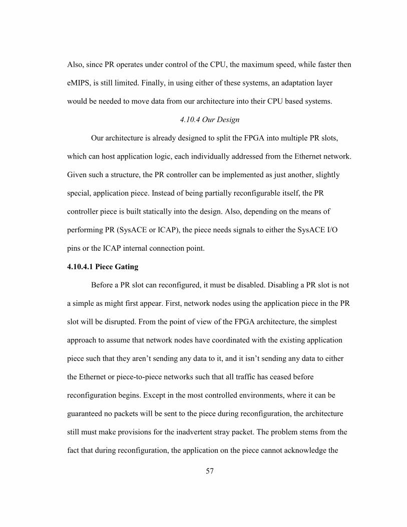
57
Also, since PR operates under control of the CPU, the maximum speed, while faster then
eMIPS, is still limited. Finally, in using either of these systems, an adaptation layer
would be needed to move data from our architecture into their CPU based systems.
4.10.4 Our Design
Our architecture is already designed to split the FPGA into multiple PR slots,
which can host application logic, each individually addressed from the Ethernet network.
Given such a structure, the PR controller can be implemented as just another, slightly
special, application piece. Instead of being partially reconfigurable itself, the PR
controller piece is built statically into the design. Also, depending on the means of
performing PR (SysACE or ICAP), the piece needs signals to either the SysACE I/O
pins or the ICAP internal connection point.
4.10.4.1 Piece Gating
Before a PR slot can reconfigured, it must be disabled. Disabling a PR slot is not
a simple as might first appear. First, network nodes using the application piece in the PR
slot will be disrupted. From the point of view of the FPGA architecture, the simplest
approach to assume that network nodes have coordinated with the existing application
piece such that they aren’t sending any data to it, and it isn’t sending any data to either
the Ethernet or piece-to-piece networks such that all traffic has ceased before
reconfiguration begins. Except in the most controlled environments, where it can be
guaranteed no packets will be sent to the piece during reconfiguration, the architecture
still must make provisions for the inadvertent stray packet. The problem stems from the
fact that during reconfiguration, the application on the piece cannot acknowledge the

58
reception of incoming packets. Left unchecked, unacknowledged packets will build up
first in the buffers for the PR slot itself, then deadlock the entire incoming Ethernet
pipeline, blocking packets destined to the PR controller. At this point, the entire
framework is stuck, as the reconfiguration process cannot complete to allow the new
application piece to acknowledge the outstanding packets, clearing the pipeline.
One solution could be to have some sort of watchdog timer, which if the pipeline
stalls for a certain amount of time resets all or part of the FPGA, throwing out all
packets. This would work since network nodes and other pieces are already supposed to
stop sending packets to a piece before the framework starts reconfiguration, so this is
just an additional safeguard that they’re doing the right thing.
A more robust solution would be that while the PR slot is being reconfigured, the
framework “drains” the PR slot. This can be done in one of several ways. One approach
is to go into a special mode where upon reconfiguration, whatever in the PR slot
wrapper’s buffers are drained, and then the PR slots wrapper’s buffers are bypassed
altogether. Once bypassed, incoming packets are immediately acknowledged with a
dummy acknowledgement.
An alternate approach is to leave the PR slot wrapper’s buffers connected in the
framework, but instead disconnect the packet ready and acknowledgement signals from
the reconfigured application piece itself, and fake a done signal as soon as a go is
received. In this method, additional power is used storing the data in the buffers, but this
may be outweighed by the simplified design since an extra sequential state machine is
not needed to handle draining the buffer before going into this mode.

59
A final question that arises is how to make the transition from reconfiguration
mode back to active mode, in the face of these stray packets. In the simplest case, any
remaining packets are fed to the new application if they are in the pipeline after it is
activated; it is up to the application to discard non-applicable packets. Alternately, the
architecture could ensure packets are flushed before activating the new piece, but this is
probably of dubious benefit, as there is always the possibility during operation that an
application may receive an invalid packet, and therefore most applications must employ
at least a minimal level of validity checking.
4.10.4.2 Architecture
Our engine uses ICAP instead of the SysACE chip due to simplicity and
performance. ICAP requires no cross-domain clocks; it can simply be driven at the same
rate as the rest of the design’s logic. Furthermore, there is no interface protocol; raw
bytes of bitstream data are fed into the port each clock cycle. The ICAP port requires no
module-external connections, as it is instantiated in HDL as a black box, which the
router connects to the appropriate FPGA-internal hard-core logic element during the
place and route phase. For this reason, the PR controller is implemented as a standard PR
application, and shares almost all the scaffolding in common with application pieces. It
shares the same two-level buffer hierarchy, and is routed by the first level MUX as
another IP addressed PR slot. Similarly, the second level dual-buffer MUX and parallel
verification unit structure is the same as PR pieces. The only difference is the final
connection to the application logic module is hard-coded in HDL, as opposed to being

60
provided by a PR module, and external signals provided for enabling or disabling PR
slots before and after reconfiguration.
Internally, the PR controller divides up application control by destination UDP
port. The PR controller is divided into two modules: one which performs the actual
reconfiguration by feeding data from network packets into the ICAP, and the other
which enables or disables PR pieces. In this prototype implementation, the protocol is
kept extremely simple. No checking is performed to ensure parameters are valid, and no
authentication is performed. PR pieces must be disabled prior to reconfiguration, then re-
enabled once again after reconfiguration is complete. The PR controller does not enforce
the ordering of this sequence of events; instead, it relies on the PC performing the
reconfiguration to ensure this constraint is not violated.
The module of the PR controller responsible for enabling or disabling PR pieces
is the gate controller, as it operates by gating dangerous signals from the pieces residing
in the PR slots which may cause invalid state to be injected into the static portion of the
design. The protocol for interfacing with the gate controller is very simple: hosts send a
single packet to the PR controller IP address, with the UDP port of the gate controller
(1235 in our implementation), with a single byte payload. The bits of this byte enable or
disable up to 8 PR slots, where a 0 is enabled, and a 1 is disabled. (This unconventional
representation stems from the fact that a 1 indicates the PR slot’s signals should be
gated). The low order bit corresponds to PR slot 0, and so forth. If the framework has
fewer than 8 PR slots, the high order bits are ignored. Every packet addressed to the PR

61
controller is echoed back to the sender with the same payload. Therefore, the sender
confirms completion of this command by receiving the exact packet back.
The actual gating of a PR slots is the responsibility of the PR slot itself. Each PR
slot wrapper contains a gate_slot signal, which the PR controller asserts. Implementation
of the gate controller is very simple; the first byte of the packet payload is copied into a
register, the bits of which are used to drive the gate_slot signals for the PR slots of the
design. Figure 8 illustrates the data flow of incoming packets of data during normal
operation versus during PR.
The actual reconfiguration is performed using the reconfiguration controller
module of the PR controller, which is addressed by another UDP port (1234). The ICAP
is configured to operate in 8-bit mode. Then, the PC performing reconfiguration simply
sends packets containing the FPGA bitstream data to the reconfiguration controller. The
controller then copies data from the packet payload, byte by byte, directly into the ICAP
controller, up to the length of the packet, then sends an acknowledgement packet back to
the host with the same data in the payload. The reconfiguration controller does not invert
the bits in the byte; but rather relies on the sending host to format the bits appropriately.
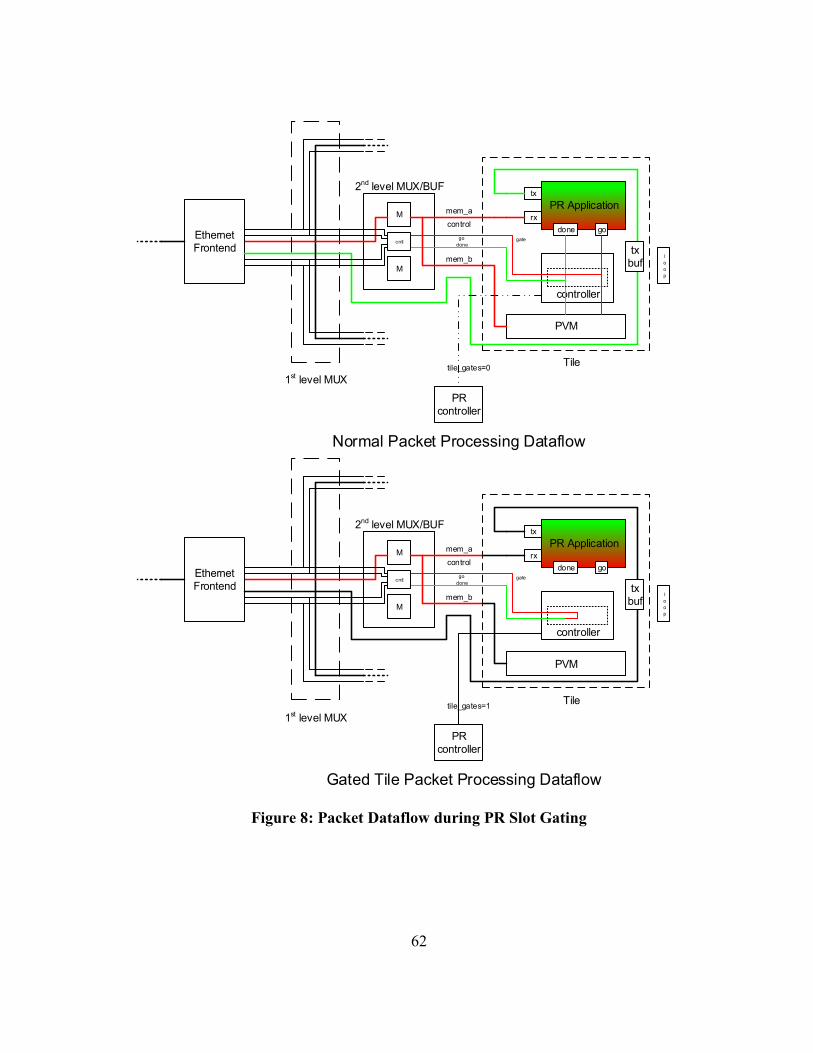
62
PR Applicationtx
PVM
controller
M
M
1st level MUX
2nd level MUX/BUF
Tile
Ethernet Frontend
mem_a
mem_b
control
PR controller
tile_gates=0
rx
gate
l
o
o
p
godone
tx buf
go
donecntl
PR Applicationtx
PVM
controller
M
M
1st level MUX
2nd level MUX/BUF
Tile
Ethernet Frontend
mem_a
mem_b
control
PR controller
tile_gates=1
rx
gate
l
o
o
p
godone
tx buf
go
donecntl
Normal Packet Processing Dataflow
Gated Tile Packet Processing Dataflow
Figure 8: Packet Dataflow during PR Slot Gating

63
5. IMPLEMENTATION AND EVALUATION
To test the feasibility of the design described in the previous section, we
constructed a prototype implementation using Xilinx FPGA XUPV5-LX110T Virtex 5
development boards. This section describes the details of that implementation, including
experiences constructing the design not appropriate for the general design section. The
development boards we used have a single Gigabit Ethernet transport and two SATA
connectors for connecting signals from GTP transceivers off-board. Therefore, the
implementation utilizes a single Ethernet link, and a daisy-chain inter-FPGA serial
topology. The design was written primarily in Verilog HDL, and synthesized, placed and
routed using the Xilinx ISE 14 software.
The design consists of four reconfigurable PR slots, distributed in area on the
chip so as to contain roughly the same number of FPGA resources (CLBs, BlockRAMs,
and DSP48). We linked three FPGAs together to form our test network. Each PR slot is
represented by a static IP address hard-coded into the design at HDL synthesis regardless
of the application piece currently active in a particular PR slot. All FPGAs in the
network live on the same subnet, and we split their tiles on nibble boundaries to reduce
the amount of logic required for the comparators in the network frontend. For this
prototype, the four PR slots of the first FPGA take the IP addresses 192.168.1.[16-19],
and the PR controller the IP address 192.168.1.20.
One goal in implementing this framework was to have it be able to sustain
processing as fast as the Gigabit Ethernet interface could send data, if the application
pieces can handle it. At the same time, we wanted to minimize complexity in the RAM

64
interfaces and keep the clock rate of the design low enough that application authors
would not have trouble place and routing their logic. Processing a byte at a time, Gigabit
Ethernet runs at a 125 Mhz clock rate. That is the rate we settled on for this design, using
byte-wide interfaces for the RAMs.
5.1 Implementation Overview
The components of the implementation closely follow the general separation of
responsibilities as laid out in the design section. These consist of BlockRAMs for
buffering the data, two frontends, PR slot wrappers, a piece-to-piece switch, and the
application pieces. The following figure shows the Verilog modules of the
implementation at a high level. As implied in the design section, moving data from the
Ethernet frontend to the pieces is simpler than in the piece-to-piece network; instead of a
fully-connected switch, a single mux routes data to and from the tiles indicated in the
diagram below as the first-level mux. Most of the framework, and all user application
pieces are in a single clock domain driven off of the Gigabit Ethernet transmission clock.
As described later, the serial interfaces require their own clock due to jitter requirements,
but that clock also runs at 125 Mhz, in sync with the main design. Finally, the receive
path of the Gigabit Ethernet PHY is driven by a clock provided by the PHY which also
runs at 125 Mhz. The Xilinx Ethernet MAC sample code provides a clock domain
crossing FIFO to bring incoming Ethernet data into transmit clock domain of the rest of
the framework. Figure 9 illustrates how these components relate to one another to form
the framework described in this thesis.

65
FPGA
PR slot
Ethernet frontend Serial frontend
Application piece
Piece-to-piece switchEthernet first-level mux
Ethernet PR slot wrapper
Block RAM
Block RAM
Piece-to-piece PR slot wrapper
Block RAM
Block RAM
FIFO FIFO
PHY RX GTP NormalClock legend
Figure 9: Overview of Framework Implementation
More specifically, the Figure 10 illustrates the flow through the implemented
framework for data received over the Ethernet interface.
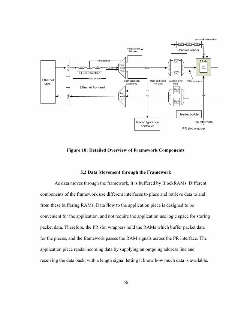
66
Ethernet
MAC
FIF
O
PR slot
apppiece
BRAMbuffer
BRAMbuffer
mux
mux
RAM interface
Header builder
valid
data stream
IP address
First-
level
mux
data
to additional
PR slots
FIF
O
Reconfiguration
controller
reconfiguration
bitstreams
tile bitstream
First-
level
mux
from additional
PR slots
BRAMbuffer
BRAMbuffer
mux
mux
MAC
Quick checker
IP UDP
Ethernet frontend
Second-level
mux
PR slot wrapper
va
lidprotocol information
MAC
Packet verifier
IP UDP
Figure 10: Detailed Overview of Framework Components
5.2 Data Movement through the Framework
As data moves through the framework, it is buffered by BlockRAMs. Different
components of the framework use different interfaces to place and retrieve data to and
from these buffering RAMs. Data flow to the application piece is designed to be
convenient for the application, and not require the application use logic space for storing
packet data. Therefore, the PR slot wrappers hold the RAMs which buffer packet data
for the pieces, and the framework passes the RAM signals across the PR interface. The
application piece reads incoming data by supplying an outgoing address line and
receiving the data back, with a length signal letting it know how much data is available.

67
For transmitting data, the piece supplies an address, data, and write enable signal along
with a length.
As data moves through the framework, it is either pushed from one module into a
RAM hosted in another, or pulled from the other module’s RAM by the destination
module. Pushing data from one module to another uses a writing RAM port, with the
address, data and write enable signals flowing from source to destination module. When
pulling data from the source module into the destination, there is no write enable signal,
and address and data lines flow in opposite directions. In the above example, the
application pulls incoming data and pushes outgoing data.
For application pieces, pulling and pushing incoming and outgoing data makes
sense, because the PR slot wrappers host the BlockRAMs so they can just connect the
piece’s signals to the RAMs directly. For the rest of the framework, it’s less clear what
type of interface to use. One straightforward case is receiving data from a serial or
Ethernet frontend into the RAMs stored in the wrappers. Here, it makes sense to use a
RAM push interface because the frontends take the data streaming in from the off-chip
links and write it into RAM buffers.
Less obvious is what to use for sending data from a wrapper to a frontend.
Sending data out the off-chip links is accomplished through IP cores which manage the
physical and data-link layers of the links. These cores use the LocalLink interface, which
provides flow control if the core needs to slow down the rate of outgoing data. The
Ethernet core doesn’t use this due to fixed size packets with an inter-frame gap sufficient
to absorb any clock rate difference between the sender and the receiver, but the Aurora

68
core does. As discussed in the design section, one possibility is to keep using LocalLink
for the outgoing interface between the PR slot wrappers and the off-chip link frontends.
In addition to the problems with fairness mentioned previously, that approach has the
problem that the LocalLink interface specifies one cycle turnaround for flow control
signals, which has detrimental effects on the clock rate as the signal are routed from a
central frontend to far reaching parts of the FPGA where the wrappers are located. Using
a RAM interface instead and letting the frontend modules provide the LocalLink to
RAM adaptation makes it easy to pipeline the signals as needed.
With a RAM interface, one possibility is to keep the design orthogonal and
provide a push interface from the PR slot wrapper to the frontend. This has the
significant advantage of making it straightforward for one application piece wrapper to
send to another: the sending wrapper simply pushes data into the receiving wrapper just
as if it were arriving from an off-chip frontend. Unfortunately, the RAM interface is not
ideal for streaming data. It does not require the sender write data sequentially, and it
provides no means of flow control to have the sender temporarily pause. Ethernet in
particular provides no provision for pausing a frame of data mid-transmission.
Therefore, the Ethernet frontend module would be forced to contain an extra BlockRAM
to buffer the outgoing data in its entirety until the sender was done before beginning to
stream it off-chip. This buffering would ensure the frontend had access to the data as
soon as it was required to send it off-chip as well as deal with flow control from the IP
core, but requires an additional scarce BlockRAM buffer for each frontend. It also adds
latency to the transmission path.

69
Due to the above reasons, for this design we decided to break orthogonality and
have the frontends pull data from the wrappers, in the same manner as the application
pieces. This lets the frontends deal with flow control without having to make another
copy of the packet. However, it does mean that sending data from one wrapper to
another is no longer trivial, as their interfaces are not compatible --- something needs to
pull data from one wrapper and push it into the other. We solve this problem by having
copier modules sit in the middle of the piece-to-piece switch. When one wrapper
indicates its destination is another wrapper on the same chip, these copier modules
stream the data out of one wrapper’s RAM and into the other.
This thesis uses two forms of control for handing off Block RAMs between
different parts of the design, as illustrated in Figure 11. In most cases the design uses
edge signaling based on a go/done signal pair, each of which is asserted for one clock
cycle, as shown in Figure 12. The second level mux uses this form of flow control to
hand off control of RAMs to the PR slot wrapper, as does the PR slot wrapper to hand
off control to the application piece. Once the sending module issues the go signal to the
destination module, ownership of the data in the RAM is transferred to the destination
module until the destination replies back with a done signal. In the interim, the sending
module maintains internal state that the destination module owns the RAM and does not
modify the RAM contents or issue another go signal until it receives the done.
In some cases we use a modified form of this flow control where the done signal
is replaced by a level triggered ready signal, with the contract that this signal falls to low
within a certain number of clock cycles after the module receives a go signal, and

70
remains low until the module has competed processing and is ready to relinquish control
of the RAM. This form of flow control is illustrated in Figure 13. Both the Ethernet
frontend and the serial frontend use this hybrid flow control for feeding data into the PR
slot wrappers. The Ethernet frontend also uses this type of flow control for transmitting
data from the pieces.
sending module
receiving module
RAM
a
d
we
a
d
go
done
Figure 11: Flow Control Model

71
0 1 2
a b c
0 1 2
a b c
send_a
send_d
send_we
go
done
recv_a
recv_d
Sender owns RAM
Receiver owns RAM
Figure 12: Go/Done Flow Control
0 1 2
IP or piece ID
a b c
0 1 2
a b c
send_a
send_d
send_we
id
ready
go
recv_a
recv_d
Sender owns RAM
Receiver owns RAM
Figure 13: Go/Ready Flow Control
72
When moving data to or from the Ethernet / Serial frontends, the flow is as
illustrated in Figure 14:
incoming
RAM
ctrl
a
d
go
done
d
we
go
done
aa
d
ready
go
d
we
go
ready
a
SwitchFrontend Tile interface App piece
to other pieces
from other frontends
outgoing
RAM
ctrl
Figure 14: Data Transport from Frontend to Application Piece
Conversely, when sending data from one piece to another, the copying logic is
illustrated in Figure 15:
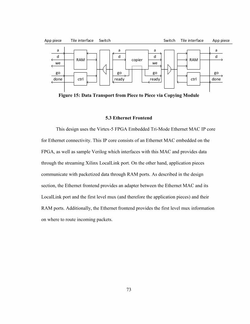
73
RAM
ctrl
a
d
go
done
d
we
go
ready
a
Switch Tile interface App piece
RAM
ctrl
a
d
go
done
SwitchTile interfaceApp piece
d
go
ready
a
copierwe
Figure 15: Data Transport from Piece to Piece via Copying Module
5.3 Ethernet Frontend
This design uses the Virtex-5 FPGA Embedded Tri-Mode Ethernet MAC IP core
for Ethernet connectivity. This IP core consists of an Ethernet MAC embedded on the
FPGA, as well as sample Verilog which interfaces with this MAC and provides data
through the streaming Xilinx LocalLink port. On the other hand, application pieces
communicate with packetized data through RAM ports. As described in the design
section, the Ethernet frontend provides an adapter between the Ethernet MAC and its
LocalLink port and the first level mux (and therefore the application pieces) and their
RAM ports. Additionally, the Ethernet frontend provides the first level mux information
on where to route incoming packets.

74
The incoming side of the Ethernet frontend works as follows. When the Ethernet
MAC indicates a packet is ready, the frontend reads enough of the packet to obtain the
IP header, but does not feed the data to the first level mux yet, instead temporarily
buffering it in a small FIFO. This is done because the information on where to route the
packet is contained in the packet itself, in the IP header. After obtaining the routing
information, the frontend then stalls the Ethernet MAC FIFO until the first level mux
indicates it is ready to accept data by asserting its rdy signal, as described in the flow
control section previously. In order to determine where to route the packet, the frontend
contains just enough logic to determine that the incoming Ethernet frame is IP/UDP, and
appears to be sent to one of the PR slots on this FPGA, but does not checksum the data.
The packet verification module in the Ethernet PR slot wrapper will perform a more
rigorous check once the data is delivered to one of its BlockRAM buffers. Figure 16
below visualizes the components comprising the frontend and the general flow of its
operation.

75
controller
1st level MUX
LL2
mem
LLFIFO
header reader
simple checker
Frontend Module
go
rdy
LL data LL data
pkt mem bus
done
go
enable
d
enable
d
Eth
M
AC LL data
ip
ver
typ
e
ud
p
mac
pkt
va
lid
rst
ip
FIFO
to tiles
Figure 16: Frontend Module Dataflow Diagram
76
5.4 ARP Resolution
In order to allow application pieces in our framework to send data to arbitrary IP
addresses, we need a way to determine the MAC address associated with an IP address.
Typically this is done using ARP. (Our prototype only supports IPv4.) In our framework
we use a simpler approach which avoids the need to create an ARP engine in HDL.
Instead, we observe the MAC address associated with IP addresses that send incoming
data to the pieces, and cache them in an array. Then, when an application piece wants to
send data, we look and see if we have the MAC address associated with the IP address
cached in our array. If so, we use that MAC address as the destination for the packet. If
we don't, we use the Ethernet broadcast address as the destination, with the hope that we
will be able to cache the MAC address if that IP address replies back with data. This
cache consists of a BlockRAM with enough space to hold 32 elements of IP address /
MAC address pairs. When an application piece wants to send a packet out to the
Internet, its PR slot wrapper queries the MAC address cache for a lookup. Multiple
wrapper’s requests are arbitrated by a module which latches each request from the
wrappers, and then services them in round-robin. Entries in the cache can be marked
permanent such that they can never be evicted by new IP addresses. These permanent
addresses are placed in the BlockRAM’s COE file and contained in the FPGA bitstream
of the framework. We use these permanent entries for containing the MAC addresses of
the server responsible for partially reconfiguring the PR slots, as well as the gateway
router to the rest of the Internet.

77
When a lookup comes in the MAC address cache iterates through each pair
which contains a valid entry, and checks to see if it matches the specified IP address.
Because the framework must run through the entire packet of data to calculate the
checksum for the IP and UDP layers, the MAC address cache has plenty of time to find a
MAC address associated with an IP address. Therefore, we opt for the simplest
implementation and simply iterate through each entry looking for a match.
New entries are added to cache by the incoming Ethernet frontend. Each time the
frontend receives a packet, it notifies the MAC address cache of the existence of a new
IP / MAC address pair. If the IP address belongs to one of the permanent entries, the
cache is done. Otherwise, if there is space in the array, it adds this pair to the first free
entry. Finally, if the array is full we use a free running counter as a random number
generator to choose which array element to evict. As a future work, it would be possible
to add usage counters to implement a form of least recently used eviction. However, at
that point it's probably better to spend the effort implementing an ARP resolver. The
received packet notifications present the only real constraint on the speed of the MAC
address cache. Ethernet packets must be at least 64 bytes long, so we know we have at
least 64 cycles to process one notification before another one can arrive. Since the cache
may need to iterate through the entire array to determine if the IP address is already
present, in addition to some overhead, we chose to make the array size 32 elements long
to avoid having to drop notifications because the cache took too long.
78
5.5 Inter-FPGA Serial Input Frontend
For inter-FPGA communication, this design uses Xilinx GTP serial transceivers
and the Xilinx Aurora IP core, which wraps the GTP transceivers and presents them as a
LocalLink port. This is the same interface used by the Ethernet MAC, and this module
serves the same purpose as the Ethernet frontend of streaming the data into and out of
the LocalLink port to and from the RAMs used by the rest of the design. Due to the low
jitter requirements of the GTP transceivers, they are driven off a different clock from the
rest of the design, and data from the application pieces needs to cross clock domains to
interface with them. This is achieved with a small LocalLink FIFO [27].
Because the two sides of a high-speed serial link do not share a common clock,
data arriving from the other chip will appear slightly faster or slower than the local
chip’s clock. Aurora handles this by providing back-pressure through the LocalLink
port. The way this is implemented is such that that Aurora can pause the LocalLink
stream mid-packet. This is inconvenient because, the same as with the Ethernet data
transfers, access to the RAMs is pipelined and data is a few cycles delayed behind the
address fed to RAM. If Aurora pauses the data transfer mid-packet (as opposed to simply
delaying the start of the next packet), this module will be a certain number of clock
cycles ahead in the RAM, and will need to rollback by this many and re-prime the
pipeline before starting again. This makes transmitting data more complicated than for
Ethernet, where the MAC does not need to temporarily interrupt the data flow, because
any differences in clock speed between the two sides of the link are absorbed by
Ethernet’s Inter-Frame Gap.

79
Aurora also supports flow control on the receiving side, pausing the sender on
the other FPGA. This could be useful for dealing with the situation where the receiving
app piece processes data slower than the sending piece, or in the case of congestion. For
this prototype we handle the problem the same way we do with Ethernet: we ignore it. If
the incoming piece-to-piece switch is not ready to accept the data, it is dropped. It is up
to the applications to detect and retry the data, and implement flow control if they desire.
In practice, the small FIFO used for crossing clock domains provides a small amount of
buffer to applications which are slow to process incoming packets before they are
dropped.
As described in the PR Slot Wrapper – Piece to Piece section, the switch on
each FPGA which accepts incoming piece-to-piece data and decides where to route it
requires the destination address be fed to it as a sideband signal. However, the variable
length source route is embedded in the incoming data stream. Therefore, this module
strips the first byte off the front of the packet as it writes the data into the RAM and
presents it to the switch as the destination address, in this way peeling the source route as
the packet travels from one FPGA to another.
5.6 Inter-FPGA Connection Topology
Having decided to use high-speed serial links separate from the Ethernet
interface to the Internet, one design question is what structure to use in connecting the
FPGAs in our network together. A full-mesh point-to-point structure would be simplest
from the point of view of routing messages from one application piece to another, and
would provide the most available bandwidth, but scales poorly, especially considering
80
that the number of high-speed serial transceivers available for implementing the links of
the mesh, while more than Ethernet MACs, is still typically in the single or double
digits. Prior work in this regard have used a ring topology (IBM) or partially-connected
mesh (Reconfigurable Computing Cluster) or a torus (Catapult).
In practice, the topology chosen is based on the connectivity offered by our
development boards. Our development board contains two SATA connectors designed
for carrying serial traffic, and so for this prototype implementation we daisy-chain the
FPGAs together in a ring. This also eases routing because if we assume the links contain
enough capacity, there’s only a single optimal direction to route packets from one board
to another — out whichever serial link gets the packet closer to the destination. The
HDL code allows more than two serial endpoints, however, so future work could extend
this to denser topologies with custom boards.
5.7 First Level Mux
The first level mux connects the Ethernet frontend to the appropriate second level
mux feeding a particular PR slot wrapper, and does so based on the packet’s destination
IP address. Both receive and transmit memory signals are switched between the frontend
and a PR slot wrapper. In the incoming (receive) direction, go/ready flow control is used
between the frontend and the wrapper, and this mux switches the go and ready signals
along with the RAM signals to the appropriate port based on the IP address the frontend
provides.
In the incoming direction, the mux simply connects memory signals to the
appropriate PR slot wrapper without requiring any arbitration. In the outgoing direction,

81
multiple PR slot wrappers provide data to the Ethernet frontend, and this module also
acts as the arbiter. The outgoing (transmit) direction also uses go/ready flow control, and
the mux currently implements a simple round-robin arbiter by cycling through each PR
slot wrapper and pulsing its rdy signal, then checking if the wrapper has data to send as
indicated by the go signal.
In the floorplan of the design on the FPGA, this module and the piece-to-piece
switch are the most timing critical as they route data from physically separate parts of
the design. All logic signals through this mux are registered, because without registration
we could not achieve timing at 125 MHz (Gigabit Ethernet line rate). This extra cycle of
delay causes no performance concerns in practice, as the memory buffers are located in
the second level mux near the PR slots, so the only module which incurs a pipeline delay
is the frontend, which sequentially streams data out of the Ethernet MAC.
5.8 Second Level Mux
In our design, the first level mux or piece-to-piece switch simply routes incoming
and outgoing data to and from the correct PR slot wrapper. At the wrapper, a second
mux handles buffering the data and presenting it to the application piece in the correct
order. The actual Block RAMs are located in this second level mux module. The
implementation follows the design as described in the On-Chip Routing section,
including the use of two buffers to allow pipelining. One difference in the actual
implementation from that of the design presented earlier allows the packet verification
module to run concurrent with the application piece. For both the packet verification
module and the application piece to access the buffer concurrently, each must use one of

82
the two ports of the Block RAMs. However, that requires sharing one of the ports with
the input from the Ethernet MAC which fills the RAM with data. An additional mux
placed in front of one of the RAM’s ports makes this possible. With this modification,
the buffer architecture now appears as shown in Figure 17:
Figure 17: Combined Verification Unit and PR Slot Wrapper Approach
This dual-RAM system is only used on the receive side. For transmission, only a
single RAM is used per PR slot. This was a deliberate design tradeoff in our prototype
system, designed to save Block RAM resources, and was based on the observation that
our sample applications consume more data from the host PC then the return back.
Therefore, transmission of reply packets takes little time compared to receiving new
data, reducing the effect of the blocking.
5.9 Piece-to-Piece Switch
The piece-to-piece switch interconnects the serial frontends and the piece-to-
piece ports of the PR slot wrappers within a single FPGA, and provides the means for
Data
Source
(Ethernet
MAC)
Data Sink
(Application
Tile)
RAM
RAM
MUX
MUXMUX
Data Sink
(Packet
Verification
Module)
Data Sink
(Application
Tile)
RAM
RAM
MUXMUX
Data Sink
(Packet
Verification
Module)

83
application pieces to send messages to one another. In this implementation it is an all-
way switch with each piece and frontend able to connect to each other with no blocking.
This simpler to design, but does consume a large amount of FPGA resources.
The switch contains 8 connections: two connections to serial frontends for either
side of the ring of FPGAs and six connections to PR slot wrappers. Only four of the
wrapper connections connect to PR slots hosting applications; the other two connect to
copying modules used when data routes through an intermediate FPGA on the way to its
final destination. Each connection consists of an incoming and outgoing RAM port, with
different interfaces for the wrapper versus serial ports. The wrapper’s incoming RAM
port pushes data from the switch to the wrapper, and the outgoing port is a pull interface.
The frontend’s connection’s, conversely, use a pull interface for their incoming port and
a push interface for outgoing. When one wrapper wants to send data to another wrapper,
the ports are no longer compatible, and internally the switch contains a copying module
which pulls data from one wrapper’s port and pushes it into the others’. There is a copier
instance for each edge in the switch which connects one PR slot to another.
Figure 18 illustrates the operation of switch. In front of each of the incoming
RAM ports for the pieces is a mux which switches the group of RAM signals incoming
from other pieces and frontends. This mux is controlled by an arbitration system
consisting of a priority arbiter, ID matcher modules, and piece-to-piece copiers. Unlike
in the Ethernet network, here we use a priority arbiter instead of round robin for
implementation simplicity. Each other piece or serial frontend connected to the switch
has the ability to generate a want signal into this arbiter, which signals the mux.

84
a
d
we
go
rdy
frontend0_a
frontend0_d
frontend0_we
frontend0_go
frontend0_rdy
piece1_a
piece1_d
piece1_we
piece1_go
piece1_rdy
frontend0_wantfro
ntend1
_wan
t
Piece 0 incoming
priority arbiter
Frontend 0 Outgoing
frontend0_go
frontend0_rdy
ID matcher
frontend0_id
frontend0_mine
ID matcher
frontend1_id
frontend1_mine
frontend0_a
frontend0_d
frontend0_we
piece0_mine
piece1_mine
piece1_go
piece1_rdy
Figure 18: Data Flow through Switch Frontend to Piece
The want signals are generated in two different ways. Both serial frontends and
pieces present a destination address which instructs the switch which piece they want to
send data to. Addresses from the serial frontends are fed to ID matcher modules for each
piece in parallel. The ID matcher for the piece with that address generates the want
signal to its local arbiter. Because there are two off-chip links and therefore two serial
frontends in our design, each piece contains two ID matchers to generate want signals

85
for the two different serial frontends to its arbiter. Want signals from other pieces are
handled by the copier modules. Because another mux already must connect the piece’s
outgoing port to the correct copier, the copier already knows which other piece is the
destination, and generates the want signal directly.
The address, data and write enable lines from the serial frontends incoming port
are connected to each piece’s mux in parallel, as they all flow in one direction from
frontend to piece. Even though the frontend does not use them currently, the switch
provides backpressure on the frontends through the rdy signal, and as a result, another
mux connects the rdy signal into the frontend to whichever piece indicated a matching
ID.
As a consequence of the means of data movement through the switch, where
frontends push data into and pull from the pieces, one frontend cannot directly send data
to another frontend when a packet needs to relay through an intermedia FPGA. The way
we solve this in this framework is to employ two additional PR slots whose only job is to
receive data from one frontend, then transmit it out the other.
5.10 PR Slot Wrapper – Ethernet Portion
The PR slot wrapper encapsulates the second level mux, the application piece,
and the supporting logic including the packet verification engine, completing the data
transport architecture.
The most significant portion of this module is the packet verification engine,
which, concurrently while the application is operating on the data, computes the packet’s
IP and UDP checksums, then compares them against the correct values stored in the

86
packet’s headers. The packet verification engine is designed in a layered fashion. Each
protocol is verified by a separate HDL module, each of which use the same memory
signals to access the packet contents. As part of the verification process, each
verification module outputs a signal indicating the length of its header in the packet. This
signal is used by the verification engine to automatically offset the address line of the
next signal. In this manner, different packet formats can be supported with minimal
effort, simply by connecting a different set of verification modules together in the
verification engine.
The wrapper also provides a packet construction engine. When given MAC, IP,
and UDP source and destination signals as well as a packet buffer with a data payload
located at an appropriate offset, it constructs packet headers for outgoing data. This
includes checksum calculations, allowing the packet to then be transmitted out the
Ethernet interface. The engine works in a similar fashion to the packet verification
module.

87
PHY
FPGA boundary
TEMAC
FIFO
Protocol Processing Unit
FIFO to
buffer
buffer
macverify
MAC
ipverify
done
valid
IP
udpverify
UDP
idextract
ID
to PRtiles
protocol
information
valid
data
Figure 19: Incoming Concurrent Packet Verification Engine
Figure 19 shows the operation of the verification engine and its modular
nature.Signals crossing the PR boundary are automatically buffered by asynchronous
partition pins in the latest Xilinx ISE 13 software, and do not require any special
handling different from ordinary signals between non-PR modules. Nevertheless, this
prototype registers all signals crossing the PR boundary. Since the packet RAMs reside
outside the PR slot, this adds one cycle to memory accesses made by the application
piece. The tradeoff for this increased latency is easier timing closure for both the static
design and application pieces, as timing closure only needs to be completed up to the
registers, which the tool has the freedom to place close to the edge of the PR slot.
Experimental experience while developing this prototype has shown that the Xilinx tools
have more difficulty with timing closure in the face of immovable PR regions as
compared to a completely static design.

88
5.11 PR Slot Wrapper – Piece-to-Piece Portion
The Piece-to-Piece portion of the PR slot wrapper serves the same role in the
design as the Ethernet portion of the wrapper by moving data to and from off-FPGA
serial links to the application pieces, but with a few changes specific to the serial links.
First, because the Aurora interface provides verification of data integrity as it travels
across the serial links, this module doesn’t need a verification unit to calculate packet
checksums; if the data arrives at this module at all, it is intact. Second, the piece-to-piece
port is used to send data that is routed between application pieces, and this module
contains the logic to add the source routes to packets before they are sent to the piece-to-
piece switch. This is implemented by an array of fixed-length registers of sufficient
length to store the longest source route needed to reach any other application piece in the
FPGA network. There is an entry in this array containing a source route for each
possible application specific ID. The implementation uses a 2-bit id signal for these IDs,
chosen as a tradeoff between allowing a sufficiently connected graph of application
pieces to be useful and minimizing the number of registers needed to hold the source
routes. For simplicity, the source route consists of a sequence of bytes, each of which
represent a serial front end or PR slot wrapper on an FPGA. This allows up to 256
addressable entities on an FPGA chip, although the current prototype only uses 8 (4
application pieces, 2 copying modules, and 2 serial front ends).
The reconfiguration controller provides the source route values stored in this
register. As part of programming the application pieces onto the FPGAs, the
configuration server sends the routes to the reconfiguration controller, which unpacks
89
the data in the Ethernet packet and directs this module to update the source route for one
of its application specific IDs with the new source route information. Because these
source routes are variable length, the exact length is determined by an end of line
sentinel, similar to C-style strings.
When the application piece initiates transmission of outgoing data, this module
appends the source route to the beginning of the application’s data. Since the transmit
RAM is hosted in the slot wrapper, and since data is pulled from the slot wrapper by the
serial frontends or copying modules, adding this variable length source route is simple to
implement with a mux which switches between presenting the source route or the actual
RAM contents, offset by the length of the source route, depending on the address
provided. As an optimization, the first destination of the route is not added to the packet
of data directly, but instead presented to the piece-to-piece switch as a sideband signal.
This is because the first hop for a packet after leaving this module is to the piece-to-
piece switch, which decides whether to send it to another piece on the FPGA or off-chip
through one of the serial links. If this module added the first route to the packet, the first
thing the switch would have to do is to pop that destination back off the front of the
packet in order to determine where to route the packet locally.

90
5.12 Client Interface
The entity which provides access to the FPGA network is a webserver
implemented in Python using the web.py framework, and users interact with the service
using HTTP GET and POST requests containing XML data. Users upload applications
as ZIP files consisting of the pieces of their application, synthesized to fit in each of the
4 possible locations on the FPGA, along with a YAML configuration file. The uploaded
application is stored locally. Once an application has been uploaded, users request the
webserver start an instance of that application. In turn, the webserver finds a space for
the instance on the FPGA network and partially reconfigures the pieces over the Ethernet
network.
To describe the interconnections between application pieces, a configuration file
authored in the YAML language accompanies the bitfiles of the application. As an
example, the application described as the example in the Interface to the FPGA
network section is described to the framework by the config file shown in Figure 20.
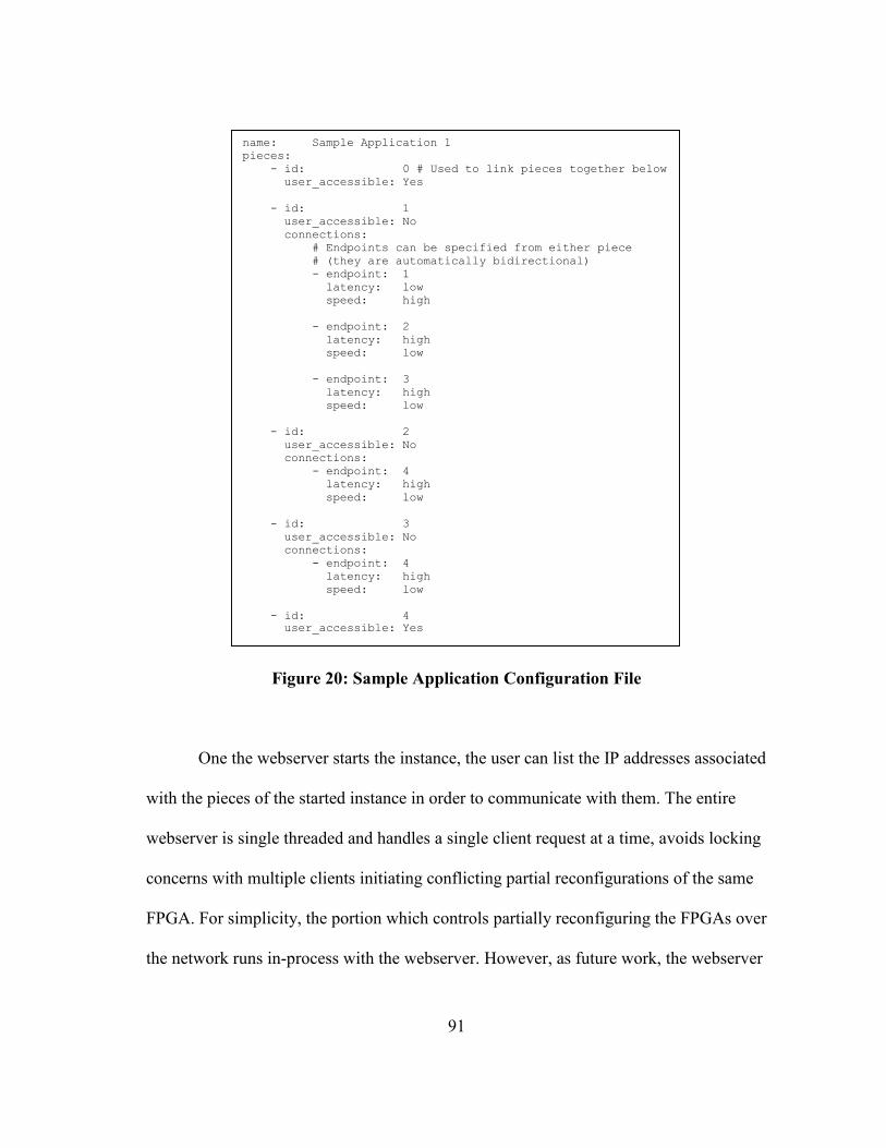
91
Figure 20: Sample Application Configuration File
One the webserver starts the instance, the user can list the IP addresses associated
with the pieces of the started instance in order to communicate with them. The entire
webserver is single threaded and handles a single client request at a time, avoids locking
concerns with multiple clients initiating conflicting partial reconfigurations of the same
FPGA. For simplicity, the portion which controls partially reconfiguring the FPGAs over
the network runs in-process with the webserver. However, as future work, the webserver
name: Sample Application 1
pieces:
- id: 0 # Used to link pieces together below
user_accessible: Yes
- id: 1
user_accessible: No
connections:
# Endpoints can be specified from either piece
# (they are automatically bidirectional)
- endpoint: 1
latency: low
speed: high
- endpoint: 2
latency: high
speed: low
- endpoint: 3
latency: high
speed: low
- id: 2
user_accessible: No
connections:
- endpoint: 4
latency: high
speed: low
- id: 3
user_accessible: No
connections:
- endpoint: 4
latency: high
speed: low
- id: 4
user_accessible: Yes

92
could be modified to take a per-FPGA lock which is only used when the reconfiguration
process is actually occurring.
5.12.1 Build System
One problem with providing multiple identical regions on the FPGA where user
logic can be partially reconfigured is that the user's logic needs to be synthesized, placed
and routed for each possible location, so that no matter where a free spot exists on the
network, the framework can place the user's logic in it. There are research projects to be
able to place and route a design into one partially reconfigurable region, then quickly
transform it to fit into other identical regions [28]. However, these solutions are not
commercially supported by FPGA vendors. Instead, for this framework we require each
application piece to be place and routed for each of the four PR slots on the FPGA. To
ease the burden this imposes on application authors, we constructed a build system based
on Python and the cog.py preprocessor which allows users to define each PR application
piece once, and have the build system implement it in each of the four PR slots. The
build system automatically pre-processes the source code to have the appropriate module
declaration for each PR slot, then automatically synthesizes, places and routes the logic
for each region. When the build process is finished, each application piece is place and
routed in each possible PR slot on the FPGA, and is ready to upload to the framework.
This build system follows the file system structure suggested by the Xilinx
Partial Reconfiguration User Guide [29]. The user places any logic pieces as subfolders
of the Source\pr folder. Each one of these subfolders is automatically pre-processed by
the build script into appropriate subfolders suitable for synthesis and place and route.
93
The build system then generates the xpartiton.tcl script outlined by the User Guide
which controls the actual synthesis and implementation.
In order for application pieces to work reliably when reconfigured onto the
FPGAs in the network, it must have been implemented against the same static design
corresponding to what is running on the FPGAs in the network. We achieve this very
simply by shipping the build system as an SDK which includes the already-implemented
bitfiles of the static portion of the design. By generating their logic against this pre-
existing bitfile, users ensure their PR logic pieces are compatible with the framework
running on the FPGAs. Updates to the base framework can be achieved by periodically
releasing new bitfiles as updates to the SDK, then slowly introducing the new version to
an increasingly larger subset of the FPGAs in the network until all users have had a
chance to recompile their applications against the design.
Before incurring expenses running their logic in the network, users will want a
way to validate that it operates correctly. We provide two options for this. First, the build
system is able to consume Ethernet data captured from Wireshark [30] and automatically
generate Verilog test harnesses which inject those packets into a simulated version of the
static portion of the framework plus the user’s logic pieces. As part of this process, the
build system generates appropriate ModelSim scripts such that the simulation can be run
with only a single command.
Second, for cases where simulation is not sufficient, by shipping the static bitfiles
used by the framework, the user can purchase a single development board of the kind

94
used in the network, then verify their design locally with the identical bitfile as will run
in the network.
5.13 Evaluation
Using the prototype implementation previously described, we conducted
evaluations to determine the usability and performance of the framework. This section
provides performance metrics of I/O bandwidth and logic utilization, as well as
experience implementing an actual application. We measured three performance metrics
about our framework. First, we measured the bandwidth available to application pieces
when communicating over the Internet as well as between pieces on the same or
different FPGAs. Second, we measured the amount of FPGA logic occupied by the
framework which is unavailable to applications and can be considered overhead of using
our framework. Finally, we obtained a rough idea of application deployment speed,
encompassing uploading an application piece to the web service and partially
reconfiguring the FPGAs.
Next, to gain experience implementing and running non-trivial real applications
on this framework, we ported the regular expression string matching hardware described
in [31] to application pieces in our framework. Although regular expressions are an
active research topic due to their ubiquity in many aspects of technology, we chose this
application due to previous experience implementing the initial version.
5.13.1 Performance Metrics
In order to test the I/O bandwidth performance of our implementation, we created
an echo application piece in Verilog and a C program running on a PC. The PC

95
application creates random packets of data consisting of the maximum size possible
which fit in an Ethernet frame, 1472 bytes of UDP payload, and sends these packets to
one of the application pieces on the FPGA. The piece is simple; when it receives a
packet from the network, it copies the data from the incoming RAM port to the outgoing
RAM port, then signals the framework to transmit the data back to the sender. The PC
application uses the standard sockets sendto() API to send UDP packets to the piece.
In order to avoid introducing variability into these benchmark results which are
designed to test the performance of the framework, we connected the test PC and the
FPGAs together on an isolated Gigabit Ethernet network. The PC application measures
how fast it can send data without packet loss. Although these tests were conducted on a
local network, the small amounts of delay in the operating system network stack and
Ethernet switch are enough to prevent pure stop-and-wait from utilizing more than a
fraction of the link’s bandwidth. Therefore, the PC application is architected to allow as
many packet as needed to be in flight between the application and the FPGAs to achieve
maximum performance.
To do this, it uses two OS threads. One thread sends UDP packets non-stop in a
loop, with a configurable delay between each packet. As described in the design section,
by convention the first four bytes of each packet are reserved for the sequence number.
For each packet sent, the application increments the sequence number. The other thread
receives incoming packets and compares the sequence numbers. If there is a gap in the
sequence, the thread notes the packet loss event in a global variable. Periodically, the
sending thread checks for packet loss, and if there hasn’t been any, decreases the delay
96
until loss occurs, thereby determining the maximum bandwidth that can be sent before
loss.
Using this application on a PC running Ubuntu 14.10 AMD64 with an Intel Core
i7-2860QM CPU nominally running at 2.50GHz, sending packets to a single application
piece on the FPGA, we can sustain 333 Mbps in both directions reliably before packet
loss occurs.
This result is substantially lower than that theoretically possible on a Gigabit
Ethernet network. To discover where the bottleneck lies, we modified the application to
send, in round-robin, a packet to the IP address of each of the four PR slots which were
configured with the echo application, as well as verify the sequence numbers for each
slot separately. Using all PR slots of an FPGA, we could sustain 980 Mbps --- almost the
entire bandwidth possible across the Gigabit Ethernet link.
This shows that the bottleneck is sending data to a single application piece, but
that if all 4 pieces are used, the framework can effectively saturate the Ethernet link. One
question these results raise is the reason that a single PR slot can only sustain 333 Mbps.
As noted earlier in the implementation section, in order to save BlockRAM resources,
the outgoing path of the Ethernet framework only uses a single RAM which is shared
between the application piece and the framework. As a result, the transmit path of any
single application piece can only sustain at best 500 of the 1000 theoretical Mbps of the
Ethernet link because while the framework is sending data from the RAM, the
application cannot be filling it with new data. This is as opposed to the incoming path
which uses two RAMs to avoid this problem. The rationale behind this decision was the

97
thought that many applications consume more data than they transmit back out over the
network (for example, processing a large incoming chunk of data, but only sending a
small status or result packet back), removing or lessening the impact of this bottleneck.
This still doesn’t fully explain why a single application piece cannot achieve 500 Mbps,
and it remains a future work to investigate further.
Finally, to test the performance of the inter-FPGA serial links, we modified the
Verilog code slightly into two variations. One variation copies data from the Ethernet
application piece port into the inter-piece port and vise-versa. The second echoes data
received from the inter-piece port back out, incrementing the address. This results in the
system as shown in Figure 21:
FPGA #3FPGA #2FPGA #1
Management Interface
PR Slot 0
192.168.1.16
192.168.1.20
Relay App Piece A
PR Slot 1
192.168.1.17
PR Slot 2
192.168.1.18
PR Slot 3
192.168.1.19
Management Interface
PR Slot 0
192.168.1.32
192.168.1.36
PR Slot 1
192.168.1.33
Relay App Piece B
PR Slot 2
192.168.1.34
PR Slot 3
192.168.1.35
Management Interface
PR Slot 0
192.168.1.48
192.168.1.52
Relay App Piece C
PR Slot 1
192.168.1.49
PR Slot 2
192.168.1.50
PR Slot 3
192.168.1.51
Serial links
Ethern
et links
Figure 21: Example Inter-FPGA Relay Test Application
With this configuration, we repeated the first experiment again, sending packets
as rapidly as possible to the one piece on FPGA 1. Again, we were able to sustain 333
Mbps without loss - the same rate as if the packets were echoed back a single FPGA, but
echoed across 3 FPGAs.

98
5.13.1.1 Logic Availability
On the XC5VLX110T FPGAs we used for our implementation, we have
configured the PR slots to occupy 54% of the slices in the FPGA. This isn’t a great
result, as it means that almost half of the FPGA is lost to overhead from the point of
view of the applications. However, this is a preliminary result chosen with a rough
estimate of the space required for the framework, as partial reconfiguration artificially
constrains the placer and router, requiring some slack compared to ideal usage
requirements. According to PlanAhead resource utilization metrics, the framework uses
only 30% versus the 46% we have allocated, so there is substantial room for
optimization of the size of our PR slots. Furthermore, the largest contribution to
framework utilization by a large factor is the piece-to-piece switch, utilizing 29% of all
LUTs comprising the framework. Therefore, one low hanging fruit for improving the
amount of logic available to the application pieces will be to rewrite that module to be
more efficient.
5.13.1.2 Reconfiguration Time
The final metric in our evaluation is the speed with which we can reconfigure a
PR slot on the FPGA. With a Python program using stop-and-wait flow control, we were
able to reconfigure a piece in 320 milliseconds. This figure could be significantly
improved by using a sliding window flow control protocol (even a window size of 2
would significantly help). However, even at current speeds the reconfiguration time is in
the same order of magnitude as many interaction with web services, and is probably low
enough not to be a bottleneck for users.

99
5.13.2 Example Application
In order to qualitatively evaluate the framework’s ability to simplify
implementing accelerated portions of computational algorithms, we ported an FPGA
regular expression matcher to our framework. Regular expressions are a language for
string matching, and today are ubiquitous due to their ability to expressively describe
complex text matching patterns. Due to their ubiquity, ways to improve their
performance are an active area of research. The CES regular expression parser used here
is an NFA-based regular expression scanner which focuses on avoiding state explosion
inherent in NFA-based engines when matching regular expressions with many or large
constrained repetitions as well as fast reconfiguration for matching different regular
expressions. CES works by transforming the regular expression into primitives
consisting of character classes with a constrained repetition qualifier. For the common
case of a string of text, each character in the string is transformed into a character class
containing a single character with no repetition. Each of these character class primitives
are implemented by a hardware module on the FPGA called a CCR.
Each CCR is fed as input an enable signal, the current character of the incoming
symbol stream, and a one bit signal indicating whether the character is in the CCR’s
character class. Internally, the CCR contains configurable logic which generates as
output a match and activation signal. This activation signal is then chained to other
CCR’s enable signals to enable matching longer regular expressions. Text input to the
system matches the regular expression if the final CCR’s match signal is true. The
aforementioned workings of CCR are illustrated in Figure 22.

100
CCR
CCR CCR CCR CCR
CCR
Shared state -> characters of string to be matched “abcd”, etc
Match signals generated by CCRsDivision between pieces
Figure 22: CES String Matching Operation
The authors of CES demonstrated the feasibility of the CCR-based approach by
building a CES scanner using a Virtex 5 FPGA. In their paper, the authors were able to
achieve high processing throughput; saturating the gigabit Ethernet link used for
communications. One limitation of the implementation, however, was scalability: the
length of a regular expression CES can match is limited by the number of CCRs which
can fit on a single FPGA. The flexibility provided by our framework provides a solution
to overcome this restriction. As longer rulesets are required, we can utilize more
application pieces in the FPGA network to implement them, even if they span multiple
FPGAs.
To implement the CES matching engine in our framework, we partition the graph
of CCRs into multiple groups, each of which is small enough to fit in a framework
application piece. Match and activation signals which span from one group to the other

101
are captured as the string is run through one group, then transported to the next group or
back to the user on the Internet using the RAM ports provided by our framework.
In order to distribute the CES grid across multiple pieces, we do need to resolve a
few details involving capturing internal state which is normally shared among all CCRs.
Specifically, the design of CES requires each character of the incoming string be
broadcast to every CCR element simultaneously each clock cycle. Then, each CCR must
look up from memory whether the current character is contained in the CCR’s character
class. Finally, each CCR may then modify its activation signal for subsequent CCRs.
This activation signal propagates asynchronously along the chain of CCRs each clock
cycle. Splitting the CCRs across pieces in our framework requires maintaining the
coherency of this asynchronous activation signal across all CCRs.
As a first step in solving this problem, we place a restriction in regular
expressions that they may not contain back references. With this restriction in place, the
interconnections between activation signals among the CCRs of the CES can be
represented as a directed acyclic graph (DAG), where each CCR is a vertex and the
directional activation signals flowing from one CCR to another the edges. Information
never flows backwards from one CCR to a previous one. By splitting the CCRs into
pieces, we are partitioning the graph into one or more cuts. Each piece can be viewed as
having two cuts in the graph: a sink cut and a source cut. The sink cut accepts as input a
character string to be matched and activation signals associated with each character in
the string, generated by the previous group’s CCRs. These are replayed into the CCRs in
the downstream group sequentially. As the incoming string and activation signals are

102
being replayed into this new group, the outgoing activation signals crossing the source
cut are captured along with the character which generated them, the same as with the
previous group. These are then sent to next group, and so on. This behavior is visualized
in Figure 23.
CCR CCR CCR
H e l l o
H H
0
H 0 0 e ...
H 0 e 1 ...
Division between pieces
Initial string to be matched, fed to first FPGA
Each clock, character and activation
signals are stored in a buffer to transmit
to next piece
One transmitted to the next FPGA in the chain, the
character and activation signals are replayed into the
CCRMs of this piece
H 0 e 1 ...
Match information is gathered into a
separate buffer and sent back to the user
over the Internet
sou
rce
sink
cut
Figure 23: Pipelining Approach to Partitioning CES across Pieces
The string and activation signal information is serialized into a buffer until the
buffer is full, then transported between pieces using the inter-piece application port. The
match process begins by the user’s computer sending a match string to the first piece in
the chain, which receives this information from the Ethernet port instead of the inter-
piece port. Similarly, the last FPGA in the chain is configured with a special state signal

103
indicating that it should capture match information instead of activation state. Its results
are then directed back to the computer for processing.
In addition to the FPGA hardware, CES as a complete system consists of a user
application which communicates with the CCR modules over the network to configure
them with information about the regular expressions, as well as feed them candidate
strings and obtain any match results. Since the initial implementation of CES resided
solely on a single FPGA, the user application only needed to map a regular expression to
available CCRs on the FPGA and update the CCR’s character class and repetition
information to configure a regular expression on the framework. Then, the app simply
sent a packet containing the string to match to the FPGA and awaited the reply.
Converting CES to run on our framework requires also requires some
modifications to this user app, which must do slightly more work. Now, when provided a
regular expression to match, the app determines the number of FPGA app pieces
required to fit the hardware CCR modules which match the regular expression. Once the
app has determined the number of pieces required, it then maps the regular expression
character classes to CCRs, the same as in the initial implementation. The new modified
app, however, knows which pieces needs to communicate with another to connect the
CCRs within the pieces together. Using this information, the app creates a configuration
file listing the number of pieces it requires and makes a web service call to the
framework, uploading the CES piece and config file and asking the framework to start
an instance of the CES pieces on the FPGA network. The framework returns a list of IP
addresses of the pieces.

104
From here, the PC application proceeds similar to the initial implementation,
configuring each of the CCRs. Finally, to match a string, the app sends the string to the
first app piece, the same as before. However, the first app piece relays match and string
information to subsequent pieces, so the final result comes from the last piece in the
chain. The current app only matches the entire regular expression provided; it does not
allow matching subsets of the regular expression. As a result, information about whether
a string matched the regular expression comes only from the last CCR module matching
the regular expression. This CCR is by definition in the last piece of the chain, and
therefore the app also looks to the last piece in the chain for match information.We
constructed the aforementioned application using Python 2.5.

105
6. SUMMARY OF FUTURE WORK
6.1 Security and Reliability
One aspect of the PR controller which is not handled in this framework is
security and access control. The PR controller on the FPGAs currently implements no
authentication or encryption. If a packet is addressed to the controller, it assumes it must
be legitimate and accepts the data. We ignore the problem for our prototype
implementation, but this is not a problem in practice, as the only entity in our framework
which should interact with the PR controllers on the FPGAs is the management web
server. The typical implementation will be to place the FPGAs and the management
server in their own trusted subnet behind a router, preventing attackers from the Internet
from spoofing packets from the Internet. Then the only threat is from a user creating a
malicious piece of logic which spoofs packets from the server. Although we do not
currently do so in our prototype, it would be easy to have the framework keep track of
the IP address of each PR slot and prevent application pieces from originating packets
from other IP addresses.
The larger, more challenging problem is ensuring that network nodes do not feed
invalid bitstreams to the PR controller. As an example, an authorized client could
accidentally feed a bitstream for the wrong PR slot, which would potentially disrupt
another user. While this scenario may be disruptive, the worst case scenario is where a
malicious client feeds a bitstream which purposely corrupts parts of the static design of
the architecture. Due to the fact that contents of FPGA bitstreams are typically kept
proprietary, it is not possible to completely verify that the bitstream only modifies the
106
proper PR slot. In a sense, this lack of protection is analogous to the early days of
multitasking PC operating systems, where programs had to simply be trusted not to
corrupt the address space of other programs.
Xilinx does partially document the bitstream to such a degree that it is possible to
determine which part of the FPGAs logic fabric will be affected at a coarse level by the
next segment of the stream. Future work should scan user bitstreams to ensure that they
only modify the proper PR slot. This validation would help catch users uploading pieces
compiled against old versions of the framework when the size of the PR slots changes
from one revision to the next, as accepting user pieces from a different version could
result in corrupting the static portion of the design. This validation alone, however, is not
sufficient to prevent malicious bitstreams from affecting other users on the FPGA, for
two reasons. First, by default the place and route algorithm may route portions of static
logic through PR slots. This is true even if we direct the router to completely avoid the
PR slots, at least for certain long interconnects with the Xilinx ISE 14 software. As a
result, an application piece could theoretically intercept another piece’s data.
More realistically, one application piece could cause denial of service to other
application pieces. This is true in the current prototype even without using invalid
bitstreams. In developed of the prototype, the biggest source of bugs stemmed from bugs
in applications loaded into one of the PR slots, which deadlocked or failed to respond to
incoming packets. If a piece deadlocks or drops packets for more than a few packets, the
entire network processing pipeline can deadlock, rendering the entire FPGA unusable to
network nodes. One potential solution is to implement a watchdog process in an external
107
chip, which checks that the static design is still operating properly, and if not, directs the
SysACE chip to reconfigure the entire FPGA from a known good bitstream.
Future work on this needs to take into account security. For the moment, it’s
probably more realistic to devote a single FPGA per customer (but still with multiple
applications) to avoid the possibility of cross-customer attacks. In particular, the
framework does not perform any validation to ensure the users are compiling against the
correct version of the static design as what’s running on the FPGAs. Even leaving aside
for the moment the issue of an attacker intentionally providing corrupted bitstreams, if
the size of the PR slots changes from one revision to the next, accepting user pieces from
a different version could result in corrupting the static portion of the design.
6.2 Scaling to 10 Gigabit Ethernet
We designed and built our prototype implementation to handle gigabit Ethernet
because that is what the evaluation boards which were available to use at the time used.
However, most modern computers are able to process a gigabit of network traffic
without issue and before too much longer the Ethernet link could start being a bottleneck
for high-performance applications, and an important next step for the design is to be able
to run at 10 gigabit speeds. The design currently pushes the limits of timing at 125 MHz,
and can therefore just barely handle gigabit throughput processing a byte at a time.
Reduction in semiconductor process size for future FPGAs will help the clock rate
somewhat, but is unlikely to provide a 10-fold improvement. Therefore, the framework
will need to move toward processing multiple bytes of data each clock cycle. Extending
the RAM ports throughout the framework to 64-bits wide would provide an 8-fold

108
reduction in required clock speed to still process Ethernet data at line rate. Moving to 10
gigabits, this would require a 156.25 MHz clock. With optimizations to the design,
combined with higher clock speeds of new FPGAs, this is probably achievable.
However, with the wider RAM ports, the routing resources occupied by the piece-to-
piece switch will become unacceptably large, and it will need to be re-designed to
something more efficient, probably a crossbar switch with some blocking probability.
109
REFERENCES
[1] Amazon.com Inc., “EC2”, http://aws.amazon.com/ec2. 2014.
[2] Google Inc., “Google App Engine”, https://developers.google.com/appengine.
2014.
[3] Microsoft Corporation, “Windows Azure”, http://www.windowsazure.com.
2014.
[4] K. Eguro and R. Venkatesan, "FPGAs for trusted cloud computing," presented at
the Proc. 2012 22nd Int. Conf. Field Programmable Logic and Applications,
Oslo, pp. 63-70.
[5] S. Byma, J.G. Steffan, H. Bannazadeh, A.L. Garcia and P. Chow, "FPGAs in the
Cloud: Booting Virtualized Hardware Accelerators with OpenStack," Proc. 2014
IEEE Symp. Field-Programmable Custom Computing Machines, Boston, MA,
USA, pp. 109-116.
[6] F. Chen, Y. Shan, Y. Zhang, Y. Wang, H. Franke, X. Chang, and K.Wang,
“Enabling FPGAs in the cloud,” Proc. 11th ACM Conf. Computing Frontiers,
Cagliari, Italy, 2014, pp. 1-10.
[7] A. Putnam., A.M. Caulfield, E.S. Chung, D. Chiou, K. Constantinides, J.
Demme, H. Esmaeilzadeh, J. Fowers, G.P. Gopal, J. Gray, M. Haselman, S.
Hauck, S. Heil, A. Hormati, J.-Y Kim, S. Lanka, J. Larus, E. Peterson, S. Pope,
A. Smith, J. Thong, P.Y. Xiao and D. Burger, "A reconfigurable fabric for
accelerating large-scale datacenter services," 41st Annu. Int. Symp. Computer
Architecture, Minneapolis, MN, USA, 2014, pp. 13-24.

110
[8] R. Sass, W.V. Kritikos, A.G. Schmidt, S. Beeravolu and P. Beeraka,
"Reconfigurable Computing Cluster (RCC) Project: Investigating the Feasibility
of FPGA-Based Petascale Computing," Proc. 2007 IEEE Symp. Field-
Programmable Custom Computing Machines, Napa, CA, USA, pp. 127-140.
[9] A.G. Schmidt, W.V. Kritikos, R.R. Sharma and R. Sass, "AIREN: A Novel
Integration of On-Chip and Off-Chip FPGA Networks," Proc. 2009 IEEE Symp.
Field Programmable Custom Computing Machines, Napa, CA, USA, pp. 271-
274.
[10] R. Baxter, S. Booth, M. Bull, G. Cawood, J. Perry, M. Parsons, A. Simpson, A.
Trew, A. McCormick, G. Smart, R. Smart, A. Cantle, R. Chamberlain and G.
Genest, "Maxwell - a 64 FPGA Supercomputer," Proc. 2007 NASA/ESA Conf.
Adaptive Hardware and Systems, Edinburgh, UK, pp. 287-294.
[11] S.W. Moore, P.J. Fox, S.J.T. Marsh, A.T. Markettos and A. Mujumdar,
"Bluehive - A field-programable custom computing machine for extreme-scale
real-time neural network simulation," Proc. 2012 IEEE Symp. Field
Programmable Custom Computing Machines, Toronto, Canada, pp. 133-140.
[12] S. Lyberis, G. Kalokerinos, M. Lygerakis, V. Papaefstathiou, D. Tsaliagkos, M.
Katevenis, D. Pnevmatikatos and D. Nikolopoulos, "Formic: Cost-efficient and
Scalable Prototyping of Manycore Architectures," Proc. 2012 IEEE Symp. Field
Programmable Custom Computing Machines, Toronto, Canada, pp. 61-64.

111
[13] K. Eguro, "SIRC: An Extensible Reconfigurable Computing Communication
API," Proc. 2010 IEEE Symp. Field Programmable Custom Computing
Machines, Charlotte, NC, USA, pp.135-138.
[14] M. Jacobsen, Y. Freund and R. Kastner, "RIFFA: A Reusable Integration
Framework for FPGA Accelerators," Proc. 2012 IEEE Symp. Field
Programmable Custom Computing Machines, Toronto, Canada, pp. 216-219.
[15] S. Liu, R. Pittman and A. Forin, “Minimizing partial reconfiguration overhead
with fully streaming DMA engines and intelligent ICAP controller”, Proc. 18th
ACM/SIGDA Int. Symp. Field-Programmable Gate Arrays, Monterey, CA, USA,
2010, pp. 292-292.
[16] P. Lieber and B. Hutchings, "FPGA Communication Framework," Proc. 2011
IEEE Symp. Field Programmable Custom Computing Machines, Salt Lake City,
Utah, USA, pp. 69-72.
[17] W. Lu, "Designing TCP/IP Functions In FPGAs," M.S. thesis, TU Delft, Delft,
The Netherlands, 2003.
[18] D. Schuehler and J. Lockwood. “A Modular System for FPGA-Based TCP Flow
Processing in High-Speed Networks,” 14th Int. Conf. Field Programmable Logic
and Applications, Leuven, Belgium, 2004, pp. 301-310.
[19] Xilinx, Inc., “LocalLink Interface Specification,” 2005.
Available: http://www.xilinx.com/products/intellectual-
property/LocalLink_UserInterface.htm

112
[20] Xilinx, Inc., “Aurora,”
Available: http://www.xilinx.com/
products/design_resources/conn_central/grouping/aurora.htm
[21] Xilinx, Inc., “System ACE CompactFlash Solution,”
Available: http://www.xilinx.com/support/documentation/data_sheets/ds080.pdf
[22] Xilinx, Inc., “Chapter 5: About Design Elements,” Virtex-5 Libraries Guide for
HDL Designs, pp. 153-155, 2011.
Available: http://www.xilinx.com/
support/documentation/sw_manuals/xilinx13_2/virtex5_hdl.pdf
[23] N. Pittman, “Extensible Microprocessor without Interlocked Pipeline Stages
(eMIPS), the Reconfigurable Microprocessor,” Master’s thesis, Dept. Computer
Science and Eng., Texas A&M Univ., 2007.
[24] Microsoft Research, eMIPS, 2013.
Available: http://research.microsoft.com/en-us/projects/emips/default.aspx
[25] Xilinx, Inc., “XPS SYSACE (System ACE) Interface Controller (v1.01a) Data
Sheet,”
Available:
http://www.xilinx.com/support/documentation/ip_documentation/xps_sysace.pdf
[26] Xilinx, Inc., “LogiCORE IP AXI HWICAP,” 2011.
Available: http://www.xilinx.com/support/
documentation/ip_documentation/axi_hwicap/v2_00_a/ds817_axi_hwicap.pdf

113
[27] Xilinx, Inc., “Parameterizable LocalLink FIFO,” 2007.
Available:
http://www.xilinx.com/support/documentation/application_notes/xapp691.pdf
[28] J.Carver, N. Pittman, and A. Forin, "Relocation of FPGA Partial Configuration
Bit-Streams for Soft-Core Microprocessors," Workshop Soft Processor Systems,
17th Int. Conf. Parallel Architectures and Compilation Techniques, Toronto,
Canada, 2008.
[29] Xilinx, Inc., “Partial Reconfiguration User Guide,” 2013.
Available:
http://www.xilinx.com/
support/documentation/sw_manuals/xilinx14_5/ug702.pdf
[30] “Wireshark: Go deep.,” 2015.
Available: http://www.wireshark.org/. [Accessed: February 20, 2015]
[31] H. Wang, S. Pu, G. Knezek and J.C. Liu, "MIN-MAX: A Counter-Based
Algorithm for Regular Expression Matching," IEEE Trans. Parallel and
Distributed Systems, 2013, pp. 92-103.
[32] A. Athavale, High-Speed Serial I/O Made Simple. San Jose, CA: Xilinx
Connectivity Solutions, 2005.
Available At http://www.xilinx.com/publications/archives/books/serialio.pdf
OTHER CONSULTED SOURCES
“Virtex-5 FPGA Configuration User Guide”,
Available: http://www.xilinx.com/support/documentation/user_guides/ug191.pdf

114
APPENDIX A
INTRODUCTION TO HIGH-SPEED SERIAL CONNECTIONS
Exchanging data between FPGAs is typically performed via custom point to
point electrical interfaces connected directly to the FPGAs. Traditionally, these links
were composed of parallel interfaces with multiple data wires latched by a common
clock signal. Certain interfaces intended for use within a single circuit board still use this
approach, notably DRAM interfaces to the memory controller on a PC or SoC system.
However, as bandwidth (and correspondingly clock speeds) increase, it suffers from the
problem of skew, where differences in impedance or length between data lines and the
clock result in bits of data arriving at different times relative to the clock signal.
Most present-day designs which need to exchange data between different pieces
of silicon transfer data serially, using transitions in the data bits themselves to convey
clock information. These interfaces embed the clock and the data together, and are
widely used for transferring large volumes of data between logic located on different
pieces of silicon. Xilinx provides a good introduction to high-speed serial I/O [32], but
in summary, it involves using one or more differential-signaled, combined clock-and-
data serial channels to convey data instead of a parallel interface and a separate clock.
High-speed serial entails more than simply taking a parallel interface and
serializing it into bits. Due to the fact that clock and data are combined, as well as the
high speeds involved, transceivers must deal with clock recovery and differences in
clock rates between chips. Combining clock and data in a single signal is achieved using
one or more bit-stuffing protocols which ensure frequent transitions in the signal. The

115
receiver uses these transitions to regenerate the sender clock. Popular serial physical
layer standards are 8b10b or 64b65b. 8b10b, utilized by the Xilinx development boards
used in this thesis, works by inserting two extra bits for every byte to ensure sufficient
transitions in the received signal even if the data has no bit transitions. Since each
endpoint of the serial link encodes their data with a local free-running clock, another
challenge is dealing with the fact that the clocks will run at slightly different rates, over
or underflowing the receivers at the other end. In 8b10b, these clock rate differences are
handled by reserving a certain percentage of the bandwidth of link for idle data (one of
the symbols in 8b10 is chosen as a “comma” symbol which denotes the idle state), and
inserting idle symbols when difference in clock rates between the two endpoints exceeds
a threshold.
The serial transceivers provided in hardware by FPGA vendors, including the
GTP transceivers provided by Xilinx on our prototype FPGAs, are typically very low
level. They usually provide 8b10b serialization and de-serialization, but not much more
than that. To create a usable interface for transferring data from HDL logic, the designer
needs to add clock compensation (inserting or removing commas from the datastream to
deal with clock rate differences), some form of clock domain crossing (usually a FIFO)
to deal with the fact that serial transceivers are usually driven from a different clock than
the rest of the design, as well as error detection and recovery. To make interfacing with
these serial transceivers easier, a variety of protocols, and libraries implementing them,
exist which operate on top of the raw hardware and implement the first few layers of the
OSI model.
116
At the data-link layer, one popular protocol is Aurora, defined by Xilinx. It
provides one or more uni-directional lanes of data presented as a LocalLink interface on
either end, provides flow control, error detection (but not error recovery), and idle
management (comma-insertion). Another widely used protocol is PCI Express. It also
defines data-link layer specification for sending packetized data across serial links (as
well as providing additional higher layers of the OSI model). On top of these data link-
layer protocols are OSI layer 3-7 type protocol suites. PCI Express fulfills this role as
well, providing transaction layer routing and quality-of-service. Another example is
RapidIO, which provide routing and application layer primitives including mailbox slots
and packetized data transfer.
For this framework we considered all of the above options. PCI Express is a
mature serial specification widely used in the PC ecosystem, but contains a large amount
of complexity stemming from its design as a local PC bus architecture which isn’t
needed for our framework. The same concern about complexity and overhead is true
with RapidIO. In the end we chose to use Xilinx’s Aurora, since our prototype uses
Xilinx FPGAs and because it adapts the serial transceivers to an interface we’re already
using for the Ethernet interfaces without providing more features our framework doesn’t
need. It also consumes a smaller amount of FPGA logic compared to PCI Express and
RapidIO.

117
APPENDIX B
TECHNICAL DETAILS OF EXTENDING CES ACROSS MULTIPLE PIECES
In order to determine how to split a CES across multiple FPGAs, an
understanding of the individual components of the CES and the data flow between them
is required. CES is composed of one or more CCR modules. Each CCR contains the
logic to match characters from an incoming string against a single regular expression
character class. By interconnecting many CCRs together, the CES gains the ability to
match an entire regular expression. Each clock cycle, the next character from the string
being matched is presented to the CES, and each CCR therein. In response to this
character and its internal state, the CCR outputs a match signal and activation signal.
The match signal indicates whether the sub-regular expressing ending with this CCR has
been satisfied for this character. The activation signal drives an input on subsequent
CCRs, and is used to modify their internal state in response to this CCRs processing of
the incoming character. The activation signal provides the mechanism for chaining
multiple CCRs together to implement a regular expression consisting of many CCR
elements.
The CES, composed of interconnected CCRs, can be represented more formally
as a graph, with nodes representing CCRs, and directed edges representing the activation
signals from one CCR to another. Additionally, each CCR node consumes an additional
input edge consisting of shared state common among all CCRs; this shared state is the
incoming character to be matched. Each CCR node also produces additional output
edges that do not connect to subsequent CCRs consisting of the match signal indicating a

118
regular expression match. Shared state input is synchronous to each clock cycle; a new
character is presented each cycle, which affects the values of the edges from one CCR to
another, as well as the match signals. Activation signals, represented by the edges
interconnecting CCRs, are asynchronous along an entire path of CCRs; a change in the
activation signal of the first CCR in a path may induce changes in every subsequent
CCR’s state and outputs within the same clock cycle. Finally, in the absence of back-
references this is a directed acyclic graph, because no CCR depends on the value of a
downstream CCR, and CCRs do not modify the global shared state; they only consume
its value.
Problem
CES as currently designed relies on operating with all elements contained within
a single clock domain, no pipelining between CCRs, and with low routing delays
between CCRs. Global shared state must propagate to each CCR, and asynchronous
activation signals must traverse multiple CCRs all within a single clock cycle. This
requirement is achievable with good performance when the entire CES design is
contained on a single FPGA, as routing delays are low and synchronization of a
relatively high-speed clock is possible. However, for large regular expressions, the size
of the CES network exceeds that of even large FPGAs. A system is needed to partition
the CES network across multiple FPGAs in a manner that maintains correctness and
performance.
Splitting the CES network into pieces and placing each piece on a separate FPGA
is analogous to making one or more cuts in the graph of CCR nodes, placing each

119
subgraph on a different FPGA, and transporting the values of the edges crossing the cut
from one FPGA to another using some off-board I/O technology.
Several properties of the CCR graph combine to make this process not entirely
straightforward. Excluding for a moment the shared state among CCRs, if the
combinatorial logic within each CCR was separated by a register at the boundary of each
CCR, it would be straightforward to treat the added delay caused by off-board I/O as if it
were a long pipeline stage in the edges of the CCR nodes crossing the cut. The different
subgraphs could concurrently process different characters, and the data from one
subgraph would arrive at the next subgraph after a delay. Unfortunately the activation
signals connecting CCR nodes are asynchronous, and not captured by a register at the
output of each CCR. These activation signals effectively group an entire path of CCRs
into the same combinatorial logic group.
In addition to the asynchronous nature of the activation signals, another problem
preventing straightforward separation of subgraphs across different FPGAs comes in the
form of shared state present to all CCRs in the CES graph. This shared state is the
current character of the string being processed, and must be fed into each CCR
concurrently, as each CCR in a path uses both this shared state and the activation signals
of previous CCRs to determine its match and activation signals. In addition to the
difficulties involved in distributing shared state among multiple FPGAs, if different
subgraphs are pipelined from one another by the long delay induced by the cut in the
graph, some of the subgraphs will see incorrect versions of the shared state relative to
the activation signals they receive from the upstream subgraph.
120
A similar problem to that of the shared state exists for the match signals
generated by each CCR node; these signals are generated relative to the current character
input as shared state to the CCRs, and are incorrect if delayed as a result of a long
pipeline.
Solution
There are several ways to solve the problems described in the previous sections.
One approach is to avoid solving the problem by synchronizing together the clocks of all
FPGAs implementing the different subgraphs, passing the signals crossing the subgraph
cuts asynchronously, and distributing the shared state to all FPGAs concurrently within
one clock cycle. Then, shared state is visible to all FPGAs simultaneously, and changes
created via an asynchronous signal on one FPGA are manifest on other FPGAs before
the clock cycle ends. The practicality of this approach is improved by the fact that edges
crossing the cut are directional, as is shared state; data does not need to move backwards
from one FPGA to its predecessors.
This approach has a practical limitation, however, of requiring the global clock
signal to be as slow as the worst-case time for signals to cross the intra-FPGA
boundaries. If the time required for signal to cross FPGA boundaries is substantially
slower than on-chip wire delays, then the performance cost of a global synchronized
clock with no pipelining will be significant.
Another approach, the one chosen by this thesis, is to decouple the clocks
between subgraphs, and solve the problems involved in pipelining signals across the cuts
in the graph. The problem of global shared state can be solved by treating it as if it were

121
a signal generated by the first subgraph, which must be passed across the cut and
pipelined in the same manner as activation signals from CCRs. Pipelining the shared
state along with the activation signals in effect delays its presence to downstream
subgraphs such that it appears along with the activation signals created in response to
that shared state.
The issue with asynchronous activation signals can be solved by treating the
pipelining process as merely extending one long clock cycle, which begins on one
subgraph and is completed on the next. In other words, so long as sufficient time is given
for the value of the asynchronous activation signal on one side of the cut of the
subgraphs to reach a steady value, it is possible to snapshot its value and represent it to
the inputs of the downstream subgraph, so long as the global shared state which induced
its value is concurrently presented to the downstream subgraph.
In a system with no cycles, the pipeline delay can be arbitrarily long because no
signals feedback. Because the CES system uses Ethernet, which has a very long latency,
and high fixed overhead per packet, a batching strategy can be employed simulating a
very long pipeline where enough clock cycles are captured to fill an Ethernet packet
before sending the date across the cut to the next FPGA.
The final problem is each CCR generates additional data in the form of match
signals which do no cross graph cuts, but instead flow into an external entity (the PC
receiving the results of the regular expression match). These match signals are only valid
in the context of the characters of shared state which induced their generation, and this
paring needs to be maintained for all CCRs in all subgraphs.
122
The straightforward solution would be for each clock cycle to pair the match
signal from each CCR in a piece with the character it is matching from the string of
incoming data, and send that data back to the user’s computer. The problem with this
approach is it consumes a larger amount of bandwidth, since for every piece, every
character is accompanied by a bit of match information for each CCR in the CES.
However, we can improve the situation by taking advantage of the fact that often, we’re
only interested in the match signal from the last CCR in the CES, as this CCR is the one
which indicates if the string matched the entire regular expression. In that case, only the
last piece needs to send match information back to the PC, making the extra bandwidth
manageable.