a neural-risc processor and parallel architecture for
TRANSCRIPT

A "Neural-RISC" Processor and Parallel Architecture
for
Neural Networks
Marco Aurelio Cavalcanti Pacheco
a thesis subm itted fo r the degree o f
Doctor of Philosophy in Computer Science
University o f London
DEPARTMENT OF COMPUTER SCIENCE
UNIVERSITY COLLEGE LONDON
September 1991
1

ProQuest Number: 10608847
All rights reserved
INFORMATION TO ALL USERS The quality of this reproduction is dependent upon the quality of the copy submitted.
In the unlikely event that the author did not send a com p le te manuscript and there are missing pages, these will be noted. Also, if material had to be removed,
a note will indicate the deletion.
uestProQuest 10608847
Published by ProQuest LLC(2017). Copyright of the Dissertation is held by the Author.
All rights reserved.This work is protected against unauthorized copying under Title 17, United States C ode
Microform Edition © ProQuest LLC.
ProQuest LLC.789 East Eisenhower Parkway
P.O. Box 1346 Ann Arbor, Ml 48106- 1346

ABSTRACT
This thesis investigates a RISC microprocessor and a parallel architecture designed to optimise the computation of neural network models. The "Neural-RISC" is a primitive transputer-like microprocessor for building a parallel MIMD (multiple instruction, multiple data) general-purpose neurocomputer. The thesis covers four major parts: the design of the Neural-RISC system architecture, the design of the Neural-RISC node architecture, the architecture simulation studies, and the VLSI implementation of a microchip prototype.
The Neural-RISC system architecture consists of linear arrays of microprocessors connected in rings. Rings end up in an interconnecting module forming a cluster. Clusters of rings are arranged in different point-to-point topologies and are controlled by a host computer. The interconnect module in each cluster acts as a communications server supporting inter-ring and inter-cluster message routing. The host, which consists of a workstation, supports network initialisation, programming and monitoring. During operation, messages in the form of packets can address: a node, a distinct group of nodes (cf. a neural network layer or cluster), all nodes (cf. broadcast), or the host. The neurocomputer nodes are configurated by downloading simple programs into each microprocessor.
The Neural-RISC node architecture comprises a 16-bit reduced instruction-set processor, a communication unit, and local memory— all integrated into the same silicon die. The processor employs 16 instructions: 11 execute in one cycle; 4 in two cycles, and the multiply instruction executes in 16 cycles. One expanding opcode branches into a set of single-cycle, memory-mapped instructions. The communication unit provides four (unidirectional) point-to-point 16-bit links and a simple protocol for routing packets. Local memory contains: a RAM memory for instructions and data; two variable length FIFO buffers (as part of the working memory) to support the communication links; and a bootstrapping ROM.
The architecture simulation studies involved the development of a software simulator and a simulation environment which entirely covered all steps in the process of programming and executing neural network models. The architecture simulator was implemented in C to aid in the design choices and to assess the proposed system. A clock-driven, register- level simulator realises each component of the Neural-RISC (system and node) architecture as configurable modules. Using the simulation environment, neural network models, written in the neural network implementation language NIL, were compiled, mapped and executed, to evaluate the system’s performance, the network addressing scheme and the processor’s instruction set.
A VLSI prototype chip was implemented to demonstrate the system and node architecture. Using the standard 2\x CMOS technology, the chip integrates an array of two Neural-RISC microprocessors. Statistical analysis based on its results, provided an assessment of the chip’s packing density and performance, and the hardware requirements of complete neurocomputer systems, for Neural-RISC chips implemented with modern CMOS technologies. Chip implementation involved the design of a customised datapath cell library, and independent PLA driven controllers for the processor and the communication units.
2

Table of Contents
ABSTRACT............................................................................................................. 2CHAPTER 1 - Introduction................................................................................. 11
1.1. Neural Information Processing.......................................................................... 11
1.2. Objectives............................................................................................................. 14
1.3. System Overview................................................................................................. 15
1.4. Research Contributions ...................................................................................... 18
1.5. Thesis Organisation............................................................................................ 20CHAPTER 2 - Neurocomputers Architectures............................................... 22
2.1. Neural Computing .............................................................................................. 22
2.1.1. Artificial Neural Networks.................................................................... 22
2.1.2. Neural Programming Environments .............................................. 27
2.2. Neurocomputers .................................................................................................. 31
2.2.1. Conventional Computer Simulators..................................................... 32
2.2.1.1. Parallel System s.......................................................................... 33
2.2.1.2. VLSI Processors.......................................................................... 35
2.2.2. General Purpose Neurocomputers........................................................ 37
2.2.2.1. Accelerator Boards .................................................................... 372.2.2.2. Processor Arrays ......................................................................... 40
2.2.3. Special Purpose Neurocomputers ........................................................ 44
2.2.3.1. Digital Implementations ............................................................ 45
2.2.3.2. Analog Implementations............................................................ 49
2.3. Summary.................................................................................................................. 51
2.3.1. System Architecture............................................................................... 51
2.3.2. Node Architecture................................................................................... 55
CHAPTER 3 - Neural-RISC System Architecture........................................... 583.1. Architectural Framework................................................................................. 58
3.1.1. S ystem Configuration............................................................................. 58
3.1.2. Expanded Systems ................................................................................. 60
3.1.3. Message-Routing System ....................................................................... 63
3.1.4. Routing Algorithm ................................................................................. 67
3.1.5. Resources Management ......................................................................... 69
3
3.2. System Operation ................................................................................................ 713.2.1. Initialisation............................................................................................. 71
3.2.2. Control & Monitoring ............................................................................ 72
C H A PTER 4 - Neural-R ISC Node A rch itectu re ................................................. 74
4.1. Processor U nit...................................................................................................... 76
4.1.1. Organisation ............................................................................................ 76
4.1.1.1. Execution U n it ............................................................................ 76
4.1.1.2. Tim er............................................................................................ 78
4.1.1.3. Interrupt Controller.................................................................... 78
4.1.2. Instruction Set ......................................................................................... 79
4.2. Communication Unit .......................................................................................... 83
4.2.1. Organisation ............................................................................................ 83
4.2.1.1. Data Ports..................................................................................... 84
4.2.1.2. I/O Buffer..................................................................................... 85
4.2.1.3. Input Arbiter ............................................................................... 86
4.3. Memory Unit ....................................................................................................... 87
4.3.1. Organisation ............................................................................................ 87
4.3.1.1. Mapping of Address Sp ace....................................................... 87
4.3.1.2. Decoding & Control Unit .......................................................... 894.4. Operation .............................................................................................................. 90
4.4.1. Processor Unit ......................................................................................... 904.4.2. Communication U n it.............................................................................. 93
C H A PT E R 5 - A rchitecture S im u la tion ................................................................. 95
5.1. Simulation Framework....................................................................................... 95
5.1.1. Software Simulator................................................................................. 96
5.1.1.1. Clock Driven S imulation ........................................................... 97
5.1.1.2. Simulated Architecture Overview ............................................ 98
5.1.2. Simulation Environment for Neural Network M odels...................... 100
5.2. Simulation Results............................................................................................... 101
5.2.1. Instruction Set Usage ............................................................................. 102
5.2.2. Communication Issues........................................................................... 105
C H A PT E R 6 - VLSI Im p lem entation ...................................................................... 108
6.1. VLSI Design Approach ...................................................................................... 108
6.2. Datapath Cell Library......................................................................................... I l l
6.2.1. Design Philosophy................................................................................ I l l
4
6.2.2. Modular Register Building Blocks....................................................... 115
6.2.3. Functional Elements............................................................................... 117
6.2.4. Interface and Switching Elements........................................................ 120
6.3. Chip Organisation............................................................................................... 1216.3.1. Operative Part Organisation.................................................................. 121
6.3.2. Control Part Organisation ..................................................................... 122
6.4. Implementation Considerations and Results ................................................... 125
CH A PTER 7 - Assessm ent .......................................................................................... 130
7.1. Neural-RISC System Architecture ................................................................... 130
7.2. Neural-RISC Node Architecture ...................................................................... 132
7.3. Architecture Simulation ..................................................................................... 136
7.4. VLSI Implementation......................................................................................... 139
C H A PTER 8 - C onclusion & Future W o r k ......................................................... 149
8.1. Summary............................................................................................................... 149
8.2. Future Work......................................................................................................... 151
R EFER EN C ES ................................................................................................................ 154
A ppendix 1 - Sam ple N eural N etw ork M o d e l..................................................... 164
A ppendix 2 - Datapath Cell L ib r a r y ....................................................................... 168
A ppendix 3 - Instruction Control S eq u en ce ................................................... 174
A ppendix 4 - M icroprocessor Schem atic D ia g r a m s.......................................... 181
*
5

List of Figures
Figure 1.1: Artificial Neural Networks............................................................................ 12
Figure 1.2: Spectrum of Neurocomputer Architectures ................................................ 14
Figure 2.1: Multilayer Neural Network........................................................................... 23
Figure 2.2: Generic Artificial Neuron.............................................................................. 24
Figure 2.3: Neuron Threshold Functions......................................................................... 25
Figure 2.4: Pygmalion Neural Programming Environment.......................................... 29
Figure 2.5: Spectrum of Neurocomputers........................................................................ 31
Figure 2.6: The Meiko Computing Surface.................................................................... 34
Figure 2.7: The Connection M achine.............................................................................. 35
Figure 2.8: General-Purpose Virtual Neurocomputer Architecture ............................ 38
Figure 2.9: TRW Mark HI ................................................................................................. 39Figure 2.10: IBM Network Emulation Processor.......................................................... 41Figure 2.11: NETSIM Neurocomputer System .............................................................. 42
Figure 2.12: CNAPS Neurocomputer.............................................................................. 44
Figure 2.13: WSI Neural Network................................................................................... 46
Figure 2.14: Conceptual Structure of W isard................................................................. 48
Figure 2.15: Analog Neural Network.............................................................................. 49
Figure 3.1: Neural-RISC System Architecture Overview............................................ 59
Figure 3.2: Scalable Communication System................................................................. 61
Figure 3.3: Average Distance for Different Cluster Configurations............................ 63
Figure 3.4: Message Packet Format................................................................................. 64
Figure 3.5: Mapping of Neural Networks........................................................................ 66
Figure 3.6: Communication Structure of Neural-RISC nodes...................................... 70
Figure 3.7: Configuration Packet Format ........................................................................ 71
Figure 3.8: Data Packet Format........................................................................................ 72
Figure 3.9: Control Packet Format .................................................................................. 72
Figure 4.1: Block Diagram of the Neural-RISC microprocessor................................ 75
Figure 4.2: Processor U n it ................................................................................................. 77
Figure 4.3: Instruction Format.......................................................................................... 80
Figure 4.4: Communication U n it...................................................................................... 84
6
Figure 4.5: Organisation of Memory U n it...................................................................... 88Figure 4.6: Distribution of the address space ................................................................. 89
Figure 4.7: Instruction Stages........................................................................................... 91
Figure 5.1: Simulation Environment ............................................................................... 101
Figure 5.2: Distribution of Instruction T ypes................................................................. 103
Figure 5.3: Instruction Frequencies ................................................................................. 103
Figure 5.4: Fragments of the Compiled Code ................................................................ 104
Figure 6.1: VLSI Design Environment............................................................................ 112
Figure 6.2: The Interconnection Structure of Cells ....................................................... 114
Figure 6.3: Schematic of the basic register. ................................................................... 116
Figure 6.4: Carry chain circuit for the A L U ................................................................... 119
Figure 6.5: Organisation of the Neural-RISC Operative Part....................................... 122
Figure 6.6: Organisation of Neural-RISC Control Part................................................. 123
Figure 6.7: Neural-RISC Clock System .......................................................................... 124
Figure 6.8: Prototype Floor Plan....................................................................................... 126
Figure 6.9: Neural-RISC Chip Layout............................................................................. 128
Figure 7.1: Mapping of Neural Networks....................................................................... 131
Figure 7.2: Simulation Environment ............................................................................... 137
Figure 7.3: Packing Density of Neural-RISC nodes...................................................... 142
Figure 7.4: Hardware Requirements for Neural-RISC Neurocomputers ................... 146
7

List of Tables
Table 2.1: Example of Neural Models Properties ......................................................... 26
Table 3.1: Control and Monitoring Commands.............................................................. 73
Table 4.1: Interrupt Sources Priority Level .................................................................... 79
Table 4.2: Instruction S e t ................................................................................................... 81Table 4.3: Memory-Mapped Instructions........................................................................ 83
Table 4.4: Network Address Checking Priority.............................................................. 87
Table 5.1: Simulated Instruction Set ............................................................................... 99
Table 6.1: Prototype Neural-RISC Features................................................................... 127
Table 7.1: General Characteristic of Neural Network Operations .............................. 134
Table 7.2: Neural-RISC Node Configurations................................................................ 142
Table 7.3: Summary of Packing and Performance Statistics........................................ 143
Table 7.4: Requirements of Multi-Ring Interconnect Modules .................................. 147
Table 7.5: Performance of Neural-RISC System s......................................................... 147
8

To a F
9

Acknowledgements
The conclusion of this work owes much to many people. Firstly, I am deeply grateful to Prof. Philip Treleaven for all support and friendship I have always received from
him throughout this work.
Secondly, I would like to thank CAPES who sponsored my postgraduate research
here at University College London.
I also would like to acknowledge my colleagues in the Computer Science Department at UCL for their advice and contributions. In particular, I wish to thank Carlo de Oliveira, Marley Vellasco, and Siri Bavan. I am also grateful to my research tutors— Charles Easteal and Dr. Russel Winder—and to the Department of Computer Science at UCL for their support and generosity. Especially, I would like to thank Prof. Peter Kir- stein, Maria Widdowson, Dr. Soren-Aksel Sorensen, and Raphael Carbonell.
I also would like to acknowledge Dr. Paul Refenes for his dedication in reading the earlier versions of this thesis and for his useful suggestions.
I wish to express my sincere thanks to Dr. Julius Leite, Prof. Carlos Jose Lucena and all my colleagues at PUC/RJ, and to Frederic S. do Couto for their truly help which allowed me to complete this work with proper conditions.
I am very much indebted to PUC/RJ, LABO Eletronica S.A. and SID Informatica S.A., Brazil, for their financial support during the last three years of this research project.
I would like to express my gratitude to various friends and relatives for their prayers, encouragement, and care received all these years. I wish to thank: mamae, papai, mano, Inez, Tete, Irma Maria Luiza, Gerarda, Tia Guiomar, and Aida. To all of you my
heartfelt thanks.
Finally, and most importantly, I want to give thanks to our Lord Jesus Christ for having given me through His graces all that I needed to complete this work: His wonderful miracles. Thanks God.
10

Chapter 1
Introduction
This chapter briefly introduces neural information processing in order to present the objectives for the design of the Neural-RISC architecture. It also presents an overview of the system, the research contributions and the organisation of this thesis.
1.1. Neural Information Processing
Neural information processing is an alternative form of computation that attempts in some ways to mimic the functionality of the human brain in solving demanding pattem- recognition problems. It divides into two distinct scientific areas: Neural Science and Neural Computing. Research in neural science branches into the study of the brain functions and the modeling of these functions. Neural scientists investigate the neurophysiology and the biophysics of biological neural networks, to determine the many complex processes involved in the neurons’ activity111.
Neural computing, on the other hand, investigates artificial neural networks, neural programming environments together with neurocomputers, and applies them to a broad class of pattern recognition problems. Pattern recognition comprises a variety of real- world problems that includes: image processing, speech processing, inexact knowledge processing, natural-language processing, sensor processing, planning, forecasting, and optimisation. For these problems, artificial neural networks exhibit a number of properties analogous to the brain: association, generalisation, parallel search, learning and flexibility^4, 8
An artificial neural network is a computing system which contains a network of highly interconnected processing elements, or PEs (Figure 1.1a). Inspired by the organisation of the human brain, these PEs contain mathematical algorithms to carry out information processing through their response to stimuli. However, processing elements used in artificial neural networks are far simpler than biological neurons. In fact, artificial
11

neurons start with simple models and functional concepts produced in neural science; complexity is added only when new knowledge is obtained or the model proves insufficient. A typical example of this is the functional model of the artificial neuron, or PE, which is a simple approximation to the electrical model of the biological neuron
(Figure 1.1b)111.
Inputs
PE
PE
PE,
Outputs
Weightss i
SummationFunction
ThresholdFunction
(a) Artificial Neural Network (b) Artificial Neuron - PE
Figure 1.1: Artificial Neural Networks
This model consists of three sections: the weighted input connections, the summation function, and a (nonlinear) threshold function that generates the PE’s output. The artificial neuron operates as a simple threshold device, depending on the state (st ) of its input elements and the connection strengths, or weights (VJ.
Many different classes of artificial neural networks exits— over 100 different types
of neural network models have already been devised*59 ’ Nearly all neural models are based on the weighted summation function79. However, there is no general model for
artificial neural networks. Essentially, models differ in specific features such as network
topology, threshold functions, and learning algorithms. There is an immense variety of learning algorithms in use today131. Some of these learning procedures work well for small tasks; new techniques are being developed to scale networks in size and to improve the training time. Learning involves extensive experimentation and fine tuning o f network parameters, such as learning rate and threshold function, that influence convergence. This requires several training runs, which are timing consuming tasks. Indeed,
12
one of the main obstacles in applying neural networks to large scale applications has been the low speed at which they operate during training in conventional computers. The availability of high performance, parallel neurocomputers is seen as the enabling solution
for developing realistic large scale neural networks.
Neurocomputers can be built from electronic hardware and optical hardware, but analog and digital electronics, being the most practical technology, predominate. Analog circuitry usually leads to smaller and more efficient implementations of arithmetic operations, and seems to be the natural choice. However, analog neurocomputers (working on
the basis of the physical analogy of a mathematical model), allows little design flexibility to experiment with the many existing classes of artificial neural networks. (Computation accuracy and sometimes the complexity of transfer functions also restrain the use of the analog approach). Digital implementations, on the other hand, tend to sacrifice speed for generality and reliability. Contrastingly, programmable, digital neurocomputers can be built as flexible, reconfigurable machines to run a variety of neural models and to cope with the advances in neural computing.
Many neurocomputer designs have already been implemented, some of them are available as commercial products122. The design approaches are depicted in Figure 1.2. They include: simulators using conventional computers, accelerator boards, processor
arrays, and dedicated hardware implementations of a specific neural network model (section 2.2 discusses these designs and presents examples). The choice of available neuro- computers varies significantly in performance and flexibility58. Neurocomputers range from flexible, general-purpose systems to high performance, special-purpose systems. An optimal neurocomputer, if such an architecture exists, lies at some point between the parameters of flexibility and performance.
Currently, most of the implementations of artificial neural networks are through general-purpose neurocomputer systems based on conventional computers. Typical designs either contain a small number of processors to implement virtual processing elements, or can only be applied to a limited set of models. In the absence of appropriate hardware, additional computational power and flexibility are obtained by using accelerator boards on serial computers or by mapping neural network models into existing parallel hardware. Some fast parallel supercomputers such as the Connection Machine, allows large applications to be attempted. However, such machines only constitute a cost- effective solution for few neural network applications. Artificial neural networks require a flexible and high performance neurocomputer architecture, that can scale according to the application size. Massively parallel, general-purpose neurocomputers can deliver
13

OptimalNeurocomputer
iSpecial-Purpose 1 General-Purpose
Neurocomputcrs • Neurocompuiers 1 / \
/ \ « / \ -— 1 -----—
P e rfo rm a n c e
ElecNe
Pro<Ar
tronicurons
:essor Co-prc rays
cessors
ConvCor
—
F le x ib ili ty
entionalnputers
Figure 1.2: Spectrum of Neurocomputer Architectures
high performance and support a wide spectrum of neural network models, thus providing a framework analogous to traditional computers. To design such machines, the RISC approach offers the benefit of small hardware implementation and, in contrast with designs that simply implement the multiply & accumulate function35*106, it provides the
flexibility of fully programmable microprocessors. Being programmable, these neuro- computers can accommodate software for neural networks such as network specification languages, which, in turn, allows the porting of applications between programming environment systems.
1.2. Objectives
The aim of this thesis is to investigate a RISC microprocessor and a parallel architecture for building a general-purpose neurocomputer. The research work involved studies in the areas of artificial neural networks, parallel architectures, VLSI design, and
RISC architectures, in order to produce a design framework. The thesis seeks to apply
the issues and requirements identified in this research to design a VLSI parallel architecture optimised for the execution of neural network models.
The main objectives for the design of the Neural-RISC architecture are summarised below:
14

• Parallelism:The neurocomputer architecture must employ real parallelism to exploit the distributed nature of artificial neural networks and to attempt the high performance
required by real-world applications.
• Performance:Overall performance must also be increased by improving the speed of individual processing elements and the bandwidth of data communication structures.
• Flexibility:To support a range of neural network models and to provide application portability, the neurocomputer must be programmable, both in terms of processing units and
node connections.
• Cost:The neurocomputer must achieve practical and cost-effective implementation using current VLSI packing density and interconnection technologies.
• Scalability:The neurocomputer architecture must scale properly in terms of VLSI design, performance and cost, so that it can be expanded into larger systems, according to the application requirements.
1.3. System Overview
This section outlines the four major parts of this research: the design of the Neural- RISC system architecture, the design of the Neural-RISC node architecture, the architecture simulation studies, and the VLSI implementation of a microchip prototype.
The system architecture comprises two basic building structures: Neural-RISC
rings and clusters of rings. A Neural-RISC ring is a linear array of identical microprocessors connected in a ring topology. Variable-size rings end up in a multi-ring interconnect module, forming a cluster. The interconnect module acts as a communications server supporting inter-ring and inter-cluster message routing. Clusters can be arranged
in diverse point-to-point topologies to achieve the optimal system size and configuration. A system composed of a number of clusters includes a host computer as the master controller. The host, which typically consists of a workstation, supports network initialisation and provides programming facilities. Each ring is crossed by two communication
15

channels, in opposite directions to reduce the distance covered by message packets. During operation, messages in the form of packets, are transferred between nodes that are logically connected. Messages are of variable length, prefixed with the address of the destination node. The system can address messages from any node to any other particular node, to a group of nodes (corresponding to a layer or a cluster, as in neural network models), to all nodes, or to the host. Downloading simple programs into each processor node configures the neurocomputer. The architecture can be scaled up to 65,536 nodes to
meet the application requirements and to achieve an optimal balance between performance and implementation cost.
The node architecture consists of a self-contained microprocessor composed of a 16-bit RISC processor, a communication unit, and a local memory. The processor adopts a reduced instruction set approach (16 instructions); an expanding opcode branches into 14 (no-operand) memory-mapped instructions. Single-cycle execution is achieved for most of the instructions by employing a simple arithmetic pipeline structure and a two- phase, nonoverlapping clock. The processor also includes a programmable timer and an interrupt controller: the timer is a 16-bit resolution count register to support timed applications; the interrupt system supports five (maskable) interrupt requests, connected in daisy chain, to attend the communication unit, the timer and the initial synchronisation of the network.
The communication unit implements a simple network, organised as a linear-array with effectively point-to-point connections. Each processor in the array is connected to each neighbour by two 16-bit links: an input and an output link. A link employs two standard handshaking signals to clock data. Separated controllers allow bidirectional communication to occur simultaneously with neighbour processors. Packets are automatically forwarded to their destination using a very simple protocol. Two (variable-length) FIFO buffers provide asynchronous transfer of packets between the
communication unit and the processor unit. The processor can access the buffers at any cycle, using any of the memory access instructions. In the Neural-RISC node architecture, processing and communication completely overlap thus relieving the I/O bottleneck frequently seen in parallel systems.
The local memory is composed of four blocks: a RAM memory for instructions and data, two data RAM blocks to implement the I/O buffers of the communication unit, and a boot-strapping ROM.
16

The architecture simulation studies provided an effective way to evaluate and to improve the design. The simulator environment consists of several modules: aconfigurable software simulator for the system and node architectures; an assembler to check instruction syntax and to generate object code to be executed by the simulator; and
the neural network implementation language (NILf) compiler to generate target machine code for the simulator. Neural network models programmed in NIL, were compiled and mapped onto the system architecture. Several alternative instruction sets were attempted based on the efficiency of the code generated by the compiler. The simulator was also instrumental in experimenting with different design strategies for the communication unit, network addressing scheme and processor interrupt system.
A VLSI prototype chip was designed and implemented in 2(i CMOS technology. Node implementation involved the specification of a number of modular datapath cells. The design of these cells was done by hand and their layout incorporated into a library. Standard cells were also used to implement parts of the chip dominated by random logic circuits. The communication unit and the processor have concurrent operation by means of independent PLA-driven controllers. The prototype chip integrates two complete Neural-RISC microprocessors in an 84-pin package. The VLSI implementation allowed us to demonstrate the Neural-RISC system and node architecture at the hardware implementation level. The results from this part of the work provided the means by what to estimate the chip’s packing density and performance for implementations with modem technologies. For example, with the 0.8|i CMOS processing technology, over 16 complete microprocessors, each with 9K bytes of memory, can be integrated into a single chip (chapter 7 gives details about this study).
For the system and node architecture we sought to combine parallelism, performance and flexibility to achieve a cost-effective design. We achieved a trade-off by providing a very simple, replicated RISC (programmable) processor as a building block of a scalable architecture.
Parallelism and performance were optimised by designing for high packing density, localised communications, and for system regularity. (Traditional RAM systems, taken
as an extreme case of VLSI parallel architectures, follow such a design approach). The structure of the linear array allows us to implement with denser technology, packing
t NIL is a programming language to specify neural network models, designed at the UCL as part of a PhD research26.
17

many processors on a chip, with no increase in the number of pins. For performance, the use of point-to-point, high-speed, unidirectional links and packet-like protocols appears to be an effective approach for multiprocessor systems. In this respect, this choice coincides with the recent IEEE standardisation project for a scalable coherent interface, which will replace the present generation of bus-based structures54,130.
Flexibility is obtained through a primitive programmable node. The design attempts the minimal implementation of a RISC architecture, which could still provide the necessary generality required by neural computing.
Finally, characteristics such as the ability to pack many processors per chip, the use
of simple communication structures, and the elimination of support chips, provide a modular growth for a highly parallel system, reducing processor and system cost.
1.4. Research Contributions
This thesis presents an effective and consistent architecture to support neural computing. In pursuing its research goals, a prime consideration has been to achieve a rational balance for the main design issues of neurocomputer architectures— parallelism, performance and flexibility. For these issues, solutions were examined and an architecture was proposed for a general-purpose neurocomputer. Using current available technology, we have demonstrated the proposed architecture, both at system and node levels, by simulating in software and by implementing a prototype chip. As with any other architecture, optimisations are possible, and some of them are discussed on chapter 7.
In summary, it is felt that the research contributions of this thesis are:
System architecture—The system architecture exhibits a compromise between wirabil- ity and performance, given the current constraints of the VLSI technology. As a homogeneous parallel system, the system architecture can be expanded to match application
requirements. Larger systems can be implemented by growing the architecture in the number of chips (or nodes per chip), number of rings and in the number of clusters. The method by which to scale the architecture can be chosen to reduce implementation cost, to optimise communication throughput, or to increase its capacity.
18
RISC architecture—The specification and design of a replicated RISC architecture to build a general-purpose neurocomputer. The architecture combines processing, interconnecting and storaging capabilities in a self-contained node design, which is clustered in many per chip. These capabilities were sized up to meet artificial neural network requirements and to comply with the design issues of performance and programmability.
VLSI chip—The chip is a demonstrative prototype which combines ideas and concepts
in the research areas of VLSI design, neural computing, parallel architectures and RISC architectures. With the prototype Neural-RISC chip, it is possible to assess silicon area, speed, etc. of future implementations with denser technologies. Consequently, it allows us to estimate the relationship between the number of integrated nodes and the node complexity (node area), for different sizes of local memory blocks, to attend specific implementations of the Neural-RISC architecture.
Modular datapath CMOS library—This includes a large number of cells customised to the design of processors’ datapaths. Cells follow a standard design for minimum silicon area and high performance. They are composed of horizontal bit-slices which team up to create: registers with customised number of bus accesses, counters (up and down), shift registers, programmable size ALUs, comparators, 3-state bus drivers, and several auxiliary logic cells.
Published work—To date, the work of this thesis has produced three research papers, accepted for publication in conferences and in the IEEE Micro1 1, ^ 2>122.
Contributions to other projects—The Neural-RISC node architecture will form the
nucleus of a general-purpose neurochip, being designed as part of another PhD research at UCL^5. This project intends to deliver an alternative design for the European Community ESPRIT project Galatea, which is concerned with development of a heterogeneous neurocomputing system.
In a second PhD research project, the Neural-RISC architecture served as test bed for the design of a neural network programming system (NPS)26. The nucleus of the programming system is a low level neural network implementation language (NIL), designed to map a spectrum of neural models onto a range of hardware platforms. NIL was implemented as a compiler that generated machine code for the Neural-RISC
19

architecture simulator. The simulator provided an effective platform to test the suitability of the language for implementing neural network algorithms on a massively parallel architecture.
Finally, the research on the Neural-RISC architecture will continue in the form of a joint cooperative project between the UCL and the Brazilian University PUC/RJ, sponsored by British Council and CNPq (Brazilian Research Funding Agency). This project, which runs for 3 years, will allow us to build a neural computer system based on the Neural-RISC architecture. A brief description of this project is presented in chapter 8.
1.5. Thesis Organisation
The remainder of this thesis is organised in seven chapters covering: neurocomputer architectures, architecture design, simulation studies, VLSI implementation, assessment and conclusion.
Chapter 2 reviews computer architectures for supporting neural networks— conventional computers, together with general-purpose and special-purpose neurocomputers. It starts by briefly examining artificial neural networks and neural programming environments, to gather design requirements. Important design features for system and node architectures are summarised and discussed at the end of the chapter.
Chapter 3 describes the architectural framework for the Neural-RISC system architecture. This includes: systems components, topology and configuration, and its mode of operation.
Chapter 4 describes the basic units of the Neural-RISC node architecture: the processor unit, communication unit and memory unit. It focuses on their organisation, architectural features and related operation.
Chapter 5 reports on the development of a simulator for the system and node architectures. It describes the simulation framework (architecture simulator and neural network programming system), presents the procedures executed for evaluation, and summarises results obtained.
Chapter 6 describes the VLSI implementation of the Neural-RISC architecture. It presents the design approach, which considered the VLSI design tools available for the
project; reports on the design of a cell library; discusses the design strategies for the
20

Neural-RISC chip; and finally, examine some design considerations and the results of the VLSI implementation.
Chapter 7 presents an assessment of the work performed in this thesis. It covers each of the main investigation aspects— Neural-RISC system and node architectures, architecture simulation and VLSI implementation; compiling and examining results.
The final chapter summarises the results of this thesis, draws some conclusions, and discusses possible future work.
21
Chapter 2
Neurocomputers Architectures
This chapter reviews computer architectures for supporting neural networks—conventional computers, together with general-purpose and special-purpose neurocomputers. Its main objective is to identify important design features for system and node architectures of neurocomputers. These features are discussed at the end of the chapter and taken into consideration for the design of the Neural-RISC architecture.
2.1. Neural Computing
Neural computing, as a technological discipline, is primarily concerned with exploiting the information processing capabilities of artificial neural networks. Although neural computing uses simple models and elements (as seen in chapter 1), an artificial neural network can take many different forms. The architecture of a neural network is made by changing certain characteristics of its basic components. The result is a formal and distinct mathematical description of the neural network, that can be freely implemented using software and/or hardware.
In this section, we present the main characteristics of artificial neural networks in order to identify design requirements for neurocomputers. Next, we review neural programming environments— neural network description languages and programming support— to collect insights from the users’ perspective.
2.1.1. Artificial Neural Networks
These networks are directed graphs represented by weighted interconnections between artificial neurons, or processing elements (PEs). These weights and the states of
the PEs represent the "data" of the network. A neural network that learns to recognise patterns does so by adjusting the weights of the connections between the PEs. A network recalls patterns based on information derived from associations already established between input and output patterns. Thus neural networks are inherently adaptive in that they conform with the imprecise, ambiguous and faulty nature of real-world data.
22

From the implementation point of view, neural networks can be characterised by a few key properties:
• network topology
• recall procedure
• training!learning procedure, and
• input values.
Network topology. The neuron interconnection pattern is perhaps the most distinguishing characteristic of a neural model. Usually, artificial neural networks have their PEs arranged into disjoint structures called layers, in which all PEs possess the same transfer function. Early models such as the Perceptron86, consist o f a single layer in which each network input is connected to all PEs. The information flows through the network from input to output, without feedback of outputs. Models of this class are called feed-forward networks. Recent models have extended this idea into structures of multiple feed-forward layers (Figure 2.1).
first secondhidden hiddenlayer layer
outputlayer
Figure 2.1: Multilayer Neural Network
In multilayer networks, middle layers are hidden from external inputs and outputs, but they receive weighted inputs (Figure 2.1). Some models have also introduced the concept of feed-backward connections. These networks improve the training-and- leaming procedure by feeding back results {errors) from a succeeding layer to a previous one.
23

To discuss the other neural network properties, we introduce the concept of a generic artificial neuron^ ,126, that incorporates the main variations of learning and recall procedures found in the different classes of neural network models. Figure 2.2 depicts the overall structure of the generic neuron. It comprises three specific functions (fl, f2, f3), a table of weights (W), and sets of input (S, E) and output (s, e) signals.
A neuron receives the input states S from other neurons, and forwards its state output s. Similarly, a set of input errors E and an error output £ provide feedback in the network. In the generic neuron, f l stands for the activation function, f l for the weight- updating function and/i for the error-calculation function.
(stateinputs)
-3*” (state output)
(weights)
(error ■<- output)
~ (error inputs)
> Activation Function: s = f l (S, W )
> Weight Updating: AW = f2 (S, e , W )
• Error Calculation: e = f3 (s, E, W )
Figure 2.2: Generic Artificial Neuron
Recall procedure. This procedure is specified by the activation function f l , which comprises the propagation rule net and the threshold function T:
net=f(S,W ) and s -T (n e t)
In its simplest form, the propagation rule calculates the weighted sum of the inputs, modified by an offset 0 that defines the neuron bias:
net = Z S . W- Q
The non-linear (threshold) function of the propagation rule calculates the neuron state. Common threshold functions (illustrated by Figure 2.3) include hard limiter, sigmoid and pseudolinear115.
24

a) Hard limiter b) Sigmoid c) Pseudo linear
Figure 2.3: Neuron Threshold Functions
Training!learning procedure. This typically iterative process presents many training pattern sets. It is, therefore, more computationally intensive than the recall procedure. Learning procedures are either supervised or unsupervised. In supervised learning the system submits a training pair, consisting of an input pattern and the target output, to the network. The network adjusts weights upon the PE’s error value (usually the difference between the expected output and the computed output of each PE) so that the difference diminishes with each cycle. Unsupervised learning procedures classify input patterns without requiring information on target output74. In such procedures, the network must detect the pattern regularities and the grouping for each applied input, to produce a consistent output.
Learning algorithms generally involve two functions (in addition to the activation function). The error-calculation function, e =f3(s,E,W), controls the updating of weights, while the function AW = f 2(S,E,W) actually updates the weights. Most models employ as weight updating function some variation of the Hebbian learning rule57. This rule states that the weight between neurons should be strengthened proportionally to their activities:
A Wij = si . sj
where s, and sj are state values, and w\j is the weight associated with the connection
between P E t and PE} . Other learning rules include the Delta rule, competitive learning, the Hopfield minimum-energy rule, the Boltzmann learning algorithm, the generalised Delta rule, and Sigma-Pi units64,115.
Input values. These are characterised according to the range they adopt— binary or continuous-valued inputs.
25

Table 2.1 summarises some of the most popular models, classified according to their functions^4 , 1 2 2 .
Neural
Network
Model
Network Topology
PE layers
Range of
input
values
Recall/Learning Procedures
Propagation
Rule
Threshold
Function
Weight
Updating
Error
Calculation
Hopfield/
Kohonen
single-layer
with
feedback
binary net= Whard
limiter AWij = S i .S j
Perceptron
single-layer
feed-forward
binary
or
continuous
net = ^S .Whard
limiter A Wij = Tpii -Zj Zj = t j - Sj
Perceptron
(Delta Rule)
single-layer
feed forwardcontinuous net = ^S .W linear A Wij = T].^' .Zj Zj = t j - Sj
Back
Propagation
multi-layer
bi-directional linkscontinuous net = W sigmoid AWij — Tl-*S,i •£/
zjo = T (net ).(tj - S j )
zjh = T (n e t) .Y £ .W
Boltzmann
Machine
multi-layer
or randomly
connected
binary net = J'\S. W sigmoid AWij =T1 .Zj Zj =T\ - {< P i j> -< p ' i j> )
Counter
Propagation
multi-layer
feed forwardbinary net =
hard
limiter
AWij i = -T\Zj i
AW ij2 = r\.Zj2
Zj i = Si - Wij i
e ;2 = Tll-6' ‘Tl2 K'«72
Self-
Organising
Map
two-dimensional
grid of
outputs PEs
continuous net = sigmoid AWij =Tl •£/ Zj = S t - Wij
Neocognitron
hierarchical
multi-layer
feed forward
continuous . . . (1 + S : W < ) , (1 + S h.W h )
linear AWij =
Notation:Wij = weight from PE t to PEj Si = state from PEi Zj = output error of PEj tj = target output of PEj T| = learning rate: 0<rj<l e = excitatory; h = inhibitory
Table 2.1: Example of Neural Models Properties
Finally, an additional class of artificial neural networks, called spatiotemporal networks, includes the time t as an extra variable in their algorithms. In other words, these neural networks deal with inputs and outputs which are explicit functions of time, i.e., S(t) and si(t). Neural networks of this class are designed specifically to classify temporal
26

pattern sequences such as speech80, or used in process control. Examples of these neural
networks are Time Delay Multilayer Perceptrons77 and Recurrent Backpropagation
model s^1.
Many other artificial neural networks are being developed to deal with a variety of real-world problems. This requires considerable experimentation, adjusting neural network characteristics to obtain an optimal network design. To design neural network
architectures and verify their results, researchers have provided software facilities that incorporate the functional structure of neural networks. These facilities include neural network description languages and a series of programming tools that are integrated into programming environments. Next section presents a brief review of these programming
environments in order to gather design requirements for neurocomputer architectures.
2.1.2. Neural Programming Environments
Neural programming environments are sets of computational tools developing and simulating neural networks models. The characteristics of these environments are mainly determined by the intended user and scope. According to the taxonomy proposed by T r e l e a v e n 1 2 ^ , neural environments can be divided into three major classes: application- oriented, algorithm-oriented, and general programming systems. In this section we review general programming systems.
Programming systems comprise a set of general programming tools and usually, an algorithm library, which can be applied to a range of applications and to other algorithms. This class of environments branches into three main categories: educational, general-purpose, and hardware-oriented systems.
Despite the variety of programming environments, a number of common features is typically found. These include:
• high-level language— to develop algorithms and applications using a highly flexible language. These are usually object-oriented languages acting in conjunction with an algorithm library to enhance programmability.
• network description language—usually an intermediate-level, machine-independent language for describing neural networks. By providing common representation of
models, these languages allow application portability. Examples of intermediate- level languages are nC, briefly described below, and NIL, which is introduced in
27

Chapter 5.
• graphic interface— this includes command menus and graphic display to control and monitor the neural network simulation. The graphic interface is often executed on a
host computer.
• algorithm library— including a set of the existing neural network models as parameterised modules.
• machine mapper—for mapping the network description language to various target
machines.
Here we examine general-purpose and hardware-oriented programming systems, which are of particular interest for this thesis.
General-purpose programming systems provide a comprehensive tool kit, targeted at different end-users who are concerned with neural network design and application development. Tools include a combination of standard features, as described above, and sometimes special hardware support (such as floating point co-processor boards and memory management), to improve system performance. We exemplify this class of environment with the Pygmalion programming system21, which is the result of a research project funded by the European Community ESPRIT Programme.
Pygmalion consists of five major parts: an intermediate-level language nC, which is a subset of C (actually a C data structure); a high level language N which is an object- oriented neural programming language based on C++; a graphic monitor based on X- windows; an algorithm library, which contains common neural models written in N ; and
a set of compilers to target UNIX-based workstations and parallel Transputer-based machines (e.g., Supernode). Figure 2.4 illustrates the structure of the Pygmalion programming environment.
The design of Pygmalion is built around a central hierarchical data structure defined in the nC language. This structure presents a view of a neural system in terms of networks, layers, clusters, neurons, and synapses (Figure 2.4). All system components (i.e., the graphic monitor, the algorithm library, and the N and nC languages) support this hierarchical structure for uniformity purposes. Neural network information is
represented in nC using four different domains: the network topology; the system’s data including neuron status and synaptic weights; the functions defining the neural network
equations; and the control of the network operation. The algorithm library includes the
28

User
High-level Language N
i\ f
Algorithms Library1 1
N
Graphics Monitor
Intermmediate Language nCtypedef s tru c t 1 ...} net_type;
typedef s tru c t { . . . ) layer type;
typedef s tru c t {. .} c lu s te r type;
typedef s tru c t {. . .1 neuron_type;
typedef s tru c t ( . . . ) synapse;
Sun, DEC
Compiler
Transputeri ------11 Neural-RISC1l________l
Figure 2.4: Pygmalion Neural Programming Environment
best known neural network models in a parameterised format. Algorithms already specify the interconnection geometry and functions but the user can select options such as the number of processing elements, their initial state, weight values, learning rates, and time constants. Neural network algorithms can be developed in N and then translated into an equivalent nC version, or can be coded directly in nC. These nC codes can be mapped onto diverse target machines for training or use. The major features of the Pygmalion programming environment are portability and practicability provided by the nC language, being a subset of the widely used C language.
Hardware-oriented programming systems emphasize the mapping of neural networks on to specific hardware. Target hardware typically includes: proprietary coprocessor accelerator boards such as the SAIC Delta88 and the HNC ANZA II61; parallel computers such as the Intel iPSC and Transputer-based systems; and silicon chips, automatically generated by dedicated silicon compilers. Currently, there is an increasing demand to port neural network applications on to parallel neurocomputers. In the absence of general-purpose (parallel) neurocomputers, additional computational power and flexibility can be obtained by mapping neural networks on to existing parallel hardware. To illustrate this approach we offer two examples: ANNE (Another Neural
29

Network Emulator) and the recent CNAPS CodeNet system (Connected Network of Adaptive Processors).
ANNE24 is a neural network simulation system targeted at an (MIMD) hypercube multicomputer system, the Intel’s iPSC. The system provides a network description language (NDL), based on Scheme (a lexical scoped version of Lisp), to describe arbitrary neural network structures. The functions executed by nodes are user-defined by
means of pointers to C routines. The NDL compiler generates: a low-level generic network specification language called Beaverton Intermediate Form (BIF); a network partition utility for mapping the neural network among the iPSC processors; and an iPSC- based neural network emulator. As part of the complete design environment ANNE supplies: a scanner/builder to construct a neural network from BIF; a message passing system to support the communication between nodes in different iPSC; a timing and synchronisation system; and user interface with monitoring facilities.
CNAPS10 is a high performance, commercial system comprising the CodeNet programming environment and the CNAPS neurocomputer. The CNAPS hardware is based on a (SIMD) linear processor array architecture (section 2.2.2.2 describes this neurocomputer). The CodeNet environment consists of: CNAPS Programming Language (CPL); the Applications Programming Interface (API); a library of function calls to enable users to embed finished CPL programs in stand-alone C applications; a windowed graphical user interface; and an algorithm library with standard neural network models. CPL is a modular programming language, with low-level access to CNAPS hardware, to create small blocks of code from which to build a large network. The CNAPS algorithm library is provided in executable and source forms. Users can create unique algorithms by combining source code modules; use any models unmodified; or modify and incorporate them in a customised program. CodeNet also includes a set of related tools to allow users to develop, debug, modify and execute CPL programs.
30

2.2. Neurocomputers
A neurocomputer is essentially a parallel array of interconnected processors that operate concurrently for emulating neural networks. Each processing unit is primitive (i.e. an analog neuron or a simple digital processor), and can contain a small amount of local memory.
When considering the set of possible architectures for the basis of a neurocomputer125, the important design issues are: parallelism , performance, cost and flexibility. These issues, which are directly influenced by the node complexity109 and the number of nodes, lead to radically different neurocomputer systems— from dedicated hardware, as simple as traditional RAM such as the Wisard system14, to programmable processors such as the Transputer, analogous in complexity to conventional computers. In the spectrum of neurocomputer architectures, the discriminative dimensions are node complexity (node area in the technology unit, X) and number of nodes, which together with network structure, establishes the system complexity (Figure 2.5).
Performance
m 10__$M RAMs
o 106__
A * Special P urpose N eurocom puters Computational Arrays
Systolic Arrays
General Purpose N eurocom puters
C onven tional Parallel C om puters
Sequential C om puters
W ' N /103 106 109 1012
Node Complexity (A2)
Flexibility
Figure 2.5: Spectrum of Neurocomputers
For these neurocomputer systems, flexibility tends to increase with node complexity, while performance can rise with number of nodes (i.e., if communications overheads do
31

not outweigh performance gains).
In the following sections we examine several examples from the spectrum of neurocomputer systems. The objective is to identify design features and capabilities for system and node architectures, which are assessed at the end of the chapter and taken into consideration for the neurocomputer design presented in Chapters 3 and 4.
2.2.1. Conventional Computer Simulators
Conventional computers support neural networks through simulation programs. Systems based on conventional computers form a subclass of general-purpose neurocomputers thus, supporting very flexible experimentation with neural networks. In these systems, a neural network is virtually simulated by time-multiplexing several PEs on each available physical processor. Performance increases with the introduction of additional processors or specialised hardware such as co-processors and high-speed memories. For such neurocomputers, the main design considerations are:
Partitioning of Neural Networks—The partitioning scheme specifies how the entire network is partitioned into disjoint sets of highly interconnected PEs, preferably of comparable sizes.
Mapping of Neural Networks—The mapping scheme attempts to minimise interprocessor communication and to equalise processing load by distributing the partitioned sets of PEs to processors, according to the size of these sets and to the distance among processors.
Processor Speed—High speed processors are necessary to avoid the processing time becoming a limiting factor, impairing the accuracy of computation when temporal characteristics of the network are important.
Processor Memory—Much memory is needed to store: weight table, output table (current state of local PEs), list of connections, lookup table for transfer functions, and other important global signals.
Interconnection Network—In parallel systems, the interconnection structure should provide sufficient bandwidth to cope with the rate of update transmissions.
32

2.2.1.1. Parallel Systems
Currently, most of the large neural network applications are being simulated on parallel systems58,124. Existing parallel systems vary largely in hardware configuration: the BBN Butterfly37 has 128 68020-nodes connected by a butterfly network, while in the BBN Plus this number doubles; the Ametek 2010110 may be configured with 1024 mesh-connected processing nodes, capable of handling 20 Mbytes/sec per link; the
Meiko Computing Surface41 allows the construction of machines from 4 to hundreds of T800 Transputers, with 1 to 12 Mbytes of memory per processor; the CM-2 Connection
Machine4,63 can contain 64K, 32K, or 16K single-bit data processors, each with 8Kbytes of local memory, connected in a regular topology, based on grids. When applied to neural network simulation, these parallel systems deliver different performance. To compare their performance requires the examination of machine characteristics and implementation strategies in great detail, together with an analysis of the neural network structures and sizes7,46.
To exemplify this, we take two contrasting cases of parallel architectures: Transputer-based systems and the Connection Machine. Both have been in common use, providing diverse application examples28,3 6 ,4 6 ,8 4 ,8 5 ,1 0 7 ,1 2 9 ,1 3 7
Transputer-based systems are medium-grained systems implementing the parallel MIMD architecture. They offer relatively cheap, simple and efficient approaches to parallel processing. There are many transputer boards available, offering different configurations to plug into microcomputer systems and workstations. An example is the Meiko In-Sun Computing Surface (Figure 2.6). The Computing Surface is a scalable, multi-processor distributed memory architecture based on the T800 transputer9. Meiko
provides a range of board level alternatives for integration within Sun workstations. Multiboards may be combined to get up to 96 transputers embedded in a single workstation, yielding from 20 to 400 (VAX) MIPS, matched by 512 Mbytes of total system memory. The most interesting feature of this system is the Electronic Message Link Switch, a proprietary VLSI routing chip, which enables applications to specify machine topology configurations at run-time (e.g., trees, grids, n-cubes, rings, and toroids). Message paths through the switch operate at the same rate as the transputer links, i.e., 20 Mbits/sec. The Computing Surface also includes: a host and fileserver interface comprising one to four
additional T800 processors with dual ported shared memory in the Sun address space, and a proprietary System Supervisor VLSI chip to support system monitoring and runtime diagnostics (Figure 2.6).
33
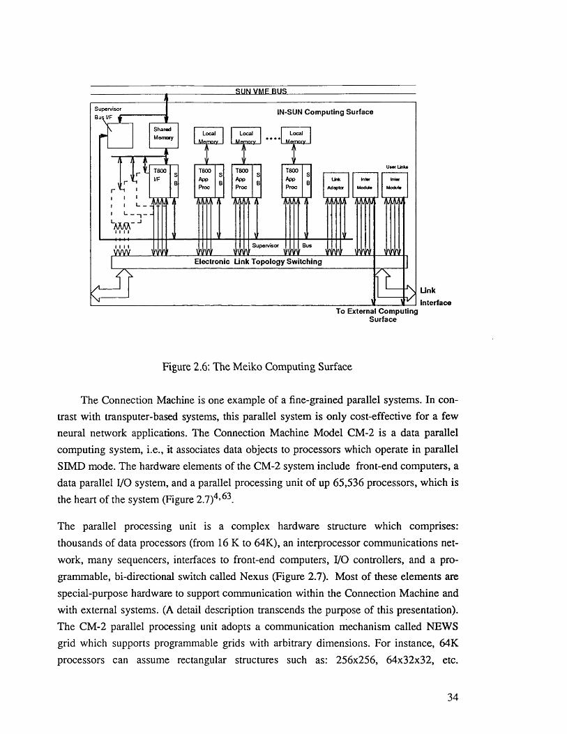
UnkInterface
To External Com puting Surface
Figure 2.6: The Meiko Computing Surface
The Connection Machine is one example of a fine-grained parallel systems. In contrast with transputer-based systems, this parallel system is only cost-effective for a few neural network applications. The Connection Machine Model CM-2 is a data parallel computing system, i.e., it associates data objects to processors which operate in parallel SIMD mode. The hardware elements of the CM-2 system include front-end computers, a data parallel I/O system, and a parallel processing unit of up 65,536 processors, which is
the heart of the system (Figure 2.7)4,63.
The parallel processing unit is a complex hardware structure which comprises: thousands of data processors (from 16 K to 64K), an interprocessor communications net
work, many sequencers, interfaces to front-end computers, I/O controllers, and a programmable, bi-directional switch called Nexus (Figure 2.7). Most of these elements are special-purpose hardware to support communication within the Connection Machine and with external systems. (A detail description transcends the purpose of this presentation). The CM-2 parallel processing unit adopts a communication mechanism called NEWS grid which supports programmable grids with arbitrary dimensions. For instance, 64K processors can assume rectangular structures such as: 256x256, 64x32x32, etc.
SIJN VME BUS
Supervisor Bu^l/F f IN-SUN Com puting Surface
SharedMemory
LocalMemory
T800AppProc
T800AppProc
T800 T800AppProc Adaptor Modiia
AMAA 1 /J f M }
"AAAA" ”*
Supervisor Busww
Electronic Unk Topology Switching
34

Nexus
<MHHt
4HHH>Connection Machine
ConnectionMachine
Processors
ConnectionMachine
Processors
Sequencer 0
Sequencer 1
Parallel Processing Unit
Sequencer 3Connection
MachineProcessors
Sequencer 2Connection
MachineProcessors
Connection Machine I/O System
Data Data DataVault Vault Vault
GraphicDisplay
Front End 0
Bus Interface
Front End 1
Bus Interface
Front End 2
Bus Interface
Front End 3
Bus InterfaceNetwork
Figure 2.7: The Connection Machine
Interprocessor communication is accomplished by message passing, supported by the router. There is one router node to each 16 processors. These router nodes are wired to form a network topology of an n-cube (e.g., a 12-cube connects 4096 processors chips). Each data processor has: 8 Kbytes of bit-addressable local memory, an arithmetic-logic unit which can operate on variable-length operands, a router interface, a NEWS grid interface, an I/O interface, and an optional floating point accelerator. The data processors are implemented using a four chip set. A fully configured CM-2 (64K processors) contains about 12,000 chips: 4096 processor chips, 2048 floating point interface chips, 2048 floating point execution chips, and 512 Mbytes of commercial RAM chips.
2.2.1.2. VLSI Processors
VLSI processors equip workstations and personal computers, which are typically employed to run neural network simulations. Performance varies largely according to the processor’s speed and whether an arithmetic co-processor is present. For instance, benchmarks of IBM PCs using multiply and accumulate operations (MAC) reveal that a 4.77 MHz 8088 can perform 102 MAC/sec, and a 16 MHz 80386 with a 80387 can reach
35

10.000 M A C / s e c 12^. Systems based on high-speed RISC processors such as SPARC, MIPS and Transputers clearly achieve better performance when emulating neural networks. Transputers are particularly attractive to use with neural networks since they are designed for parallel processing. The 20-Mhz T800 transputer can produce rates of over180.000 MAC/sec, three times faster than a 20-MHz Intel 80386 with a 80387 coprocessor7 . Using a hand-optimised assembly language code, this rate can exceed600.000 MAC/sec78. (Additional improvement in speed is still possible by taking the advantage of the internal RAM and by using different implementation strategies). Here, we shortly review the main transputer features.
The Transputer is a single chip 32-bit microprocessor that supports concurrent processing via the Ocean programming model66,133. A transputer contains a processor, local memory, and four point-to-point communication links— all integrated into one silicon chip. An external memory interface extends the on-chip memory. When necessary, the transputer also includes a special-purpose processing and interface hardware. The T800 model has both an internal 32-bit integer processor and an internal 32-bit floating point unit. The 20 MHz version of the T800 (10 MIPS and 1.5 MFLOPS) has 4 Kbytes of internal RAM, and supports a 32-bit external memory interface (32-bit address space and data). The device also provides a couple of timers and a fast interrupt system. The
instruction format uses compact encoding based on 1-byte instructions— 4-bit opcode and constants between 0 and 15. (Prefixing instructions are used to form operands longer 4 bits)93.
Communications are performed by one-way channels. A channel between two processes in the same processor is implemented using a single memory location. If the channel exits between two different processors then it is implemented using a point-to- point link. There are four pairs of 20 Mbits/sec serial links on the T800 (half of them to transmit, half to receive). A transputer can therefore be attached to a maximum of four
other transputers at a time. Communications are synchronised using a simple protocol which introduces start and stop bits and acknowledgement messages. The maximum
theoretical data transfer rate between the T800’s is therefore 1.7 Mbytes/sec (2.4 Mbytes/sec when both links are used simultaneously).
Transputers have been designed to support general-purpose, parallel, medium- grained computing systems. Features such as large instruction and data cache memory, wide data and address buses, floating point unit, and support for scheduling processes, surpass the requirements of a single neural network processing element. Meanwhile, new process technologies have been used to enhance the transputer features (for instance,
36

the new Transputer INMOS T9000 has a 16K byte cache and 64-bit address bus)1-^.
Neural networks require massive parallelism and simpler processor nodes thus, recom
mending architectures that exploit the VLSI properties to optimise these design issues.
2.2.2. General Purpose Neurocomputers
General-purpose neurocomputers are programmable computers for emulating a wide spectrum of neural network models. Figure 2.8 shows their general architecture, as
proposed by Hecht-Nielsen58. The structure resembles a parallel array processor, comprising R identical processors connected through an interconnection network. Each physical processor executes a section of the "virtual" network. To program the neuro- computer, the virtual PEs are partitioned across the local memories of the physical processors. Computing a neural network involves a continuous updating of the states of the virtual PEs. Updating a virtual PE implies broadcasting the update through the network. Processors that need access to that information accept and store the update in their local system state memory. Computation, therefore, is carried out through a sequence of iteration cycles. Next iteration occurs in lock-step, i.e., when all other processors have completed the previous one.
General-purpose neurocomputers can be further subdivided into accelerator coprocessors boards/fl and parallel processor arrays124. Commercial co-processors are typically floating-point or signal processing accelerator boards, usually supplied with a large memory (for instance 4 Mbytes). These boards plug into the backplane of an IBM PC or interface to a SUN Workstation or a DIGITAL VAX. Parallel processor arrays are cellular arrays109, composed of a large number of primitive processing units, connected
in a regular—and usually restricted— topology.
2.2.2.I. Accelerator Boards
Hardware accelerators, such as the HNC ANZA60, the SAIC SIGMA-188, and the NEC Neuro-07, have allowed neural network experiments to be carried out over 100 times faster than simulators on conventional computers. These programmable systems can implement large networks of virtual processing elements with a limited number of hardware-implemented processors. Designers usually implement the processors by means of an industry-standard signal processing chip (e.g., the TMS320) or a microprocessor such as the MC68020 (and its MC68881 floating point co-processor),
37

Interconnection N etw ork
NetworkInterface
NetworkInterface
NetworkInterface
Local System State Copy
PhysicalProcessing
Unit
Local System State Copy
Local System State Copy
PhysicalProcessing
Unit
PhysicalProcessing
Unit
System Controller
Virtual PE Interconnect and Weight
Memory
Virtual PE Interconnectand Weight
Memory
Virtual PE Interconnect
and Weight Memory
External Computer Interface
Figure 2.8: General-Purpose Virtual Neurocomputer Architecture (from Hecht-Nielsen)58
interconnected through a standard parallel broadcast bus such as the VME bus. Physical processors and interconnections are multiplexed across a large number of virtual processing elements and virtual interconnections, and demand large memories to be represented. Performance comparisons between these products are based on capacity (the maximum size of neural network) and speed (the time to process a neural network). Speed is usually expressed in network connection updates per second (CPS), for both the training
phase and the recall phase. For instance, the ANZA Plus supports 1M PEs with 1M interconnections, and is capable of 1.5M connection updates per second during training and 6M updates during recall.
Here, we examine two earlier examples of hardware accelerator boards: the TRW MARK neurocomputer family and the SAIC Delta.
The TRW neurocomputer f a m i l y ^ * 75 includes the Mark II software simulator, the Mark III co-processor and the Mark IV high-speed neurocomputer. All share the
38

common Artificial Neural System Environment (ANSE) user programming system.
The Mark III consists of up to 15 single-board computers, each built from a Motorola MC68020 microprocessor and a MC68881 floating point co-processor, all connected to a VME bus (Figure 2.9). The system is designed for network partitioning across the processor boards. Information to perform each network connection is localised to each board. This minimises bus traffic which in turn allows a number of processors to share the bus. To allow broadcast operation and to increase the bus bandwidth, the VME
bus was slightly converted (transmissions on the bus to memory locations within a address block are received by all processors boards), and a custom VME bus controller was introduced. Currently, the Mark III supports 65,000 virtual processing elements and over 1 M trainable interconnections, with a performance of 4.5 mega connection updates per second.
VME BUS
6802068881
6802068881
6802068881
MemMem Mem DMAI/O
VAX
VME BUS
Arbiter
and
Serial
I/O Ports
to VAX
Slave 1 Slave n Slave MasterController
Figure 2.9: TRW Mark III
The Mark IV neurocomputer is a one module system, consisting of a single highly pipelined processor. It was constructed out of signal processing building blocks (i.e., adders, multipliers, memories and barrel shifters), TTL and memory chips. In the Mark IV the execution of all neural network functions (i.e., weight update, threshold, and error calculation functions) occurs simultaneously on each 200 ns clock cycle. The Mark IV
supports 256,000 virtual PEs and 5.5M interconnections, and a speed of 5M CPS (with learning) for any model it could implement61.
39

The SAIC (Science Applications International) Delta II is a high speed single-board commercial emulator for PC environments8,88,1-4. The board contains a single fast (ECL technology) floating point processor, optimised for neural network emulation. The
Delta floating point processor architecture has several novel features which makes it one the most powerful accelerator boards. The processor employs a 3-4 stage pipelined Harvard architecture (instruction fetch, decode and operand fetch, multiply, and accumulate), and parallel internal buses to feed the ALU/multiplier. It is able to execute 32-bit floating point multiply and accumulate operations at clock speeds which translates 22 MFLOPS peak rate. The memories used are 1M bit static column-mode chips. These chips are organised as 1024 segments of 1024 bits per segment. The fast (35 ns) static column
mode of access provides a significant improvement in speed, in contrast with the successive words in memory, found in most network simulators. The Delta instruction set includes approximately 1900 instructions which provide full support for 32 and 64 bit integer and floating point arithmetic. Array instructions employ hardware loop counter and memory pointers to perform up to 1024 arithmetic operations from a single array instruction. A full set of logical, control (jump, jump-to-subroutine, return), and 15 condition code flags are included. Most instructions execute in a single cycle (93 ns), with the exception of square root, double precision divide, conditional and stores. The Delta processor supports 3.1M PEs and interconnections, and has achieved a processing rate of 2.7M CPS in Backpropagation learning and 11M CPS in forward propagation.
2.2.2.2. Processor Arrays
General-purpose neurocomputers based on parallel processor arrays actually constitute a natural evolution from the co-processors boards discussed above. Parallel processor arrays optimise neural processing by distributing the network through a large number
of simpler processors. Some processor arrays are built from replicatable boards, frequently employing an industry-standard microprocessor chip. Other projects are developing their own custom-designed neuro-microprocessor. In general, the small local memory associated with each physical processor accommodates only a reduced number
of virtual PEs, determined by the complexity of the neural algorithm.
Research groups in the USA, Japan and Europe have operational parallel neurocomputers and many more parallel processor array architectures are under development122. They basically differ in three aspects: the processor’s grain level (that is, the number of processors), the processor’s complexity, and the interconnection geometry. Below we
40

review the IBM NEP, the TI(UK) and Cambridge NETSIM, and the Adaptive Solutions CNAPS.
The Network Emulator Processor (NEP) is part of a complete network programming environment called CONE (Computation Network Environment)32,5 , developed
at IBM’s Scientific Center in Palo Alto. NEP is a cascadable unit which acts as coprocessor for a PC host. It can be cascaded to up 256 NEPs, in a unidirectional interprocessor communication network to support a total of 1M virtual PEs and 4M interconnections. NEP is based on the 5 MIPS TMS320 digital signal processor (Figure 2.10). The unit includes a 64K x 16-bit SRAM data memory, a 4K x 16-bit SRAM program
memory, an 80 Mbytes/sec local I/O interface, a global interface to the PC host, and a 100 Mbytes/sec inter-NEP NEPBUS interface.
Local NEPBUS NEPBUS Localout-port out-port in-port in-port
NEP Internal B uses
Receive MUX
TMS320
LocalTransmit
FIFO
ReceiveFIFO
NEPBUSTransmit
FIFO
Generator
Address
Host Interface (IBM PC)
WritableControlMemory
Control LogicData Memory (RAM)
Figure 2.10: IBM Network Emulation Processor
Each NEP can simulate about 4K virtual PEs and 16K interconnections, with 30-50 total network updates per second. The length of a network update cycle can be reduced by partitioning the network across a number of NEPs32.
NETSIM is a project developed by Garth45 of Texas Instruments (UK), working with Cambridge University. The NETSIM system consists of a collection of neural
41

network emulator cards ("NETSIM" cards) arranged in a 3-dimensional array structure, with a PC host acting as a system controller. Each NETSIM card is an autonomous single-board processing unit based on an industry-standard microprocessor and
specifically designed to solve neural network models. It consists of: a local microprocessor (Intel 80188) and associated program memory; two custom chips— a "solution engine" (the simulation element) and a communication processor; a synapse/input memory; and a BIOS in EPROM. A large number of such card can be connected via message passing network to form a system (Figure 2.11).
3-D array of NETSIM cards
hostcomputer
solution engine chip
communicationschip
localmicroprocessor
memory
Figure 2.11: NETSIM Neurocomputer System
The Solution Engine operates as a back-end vector co-processor for the local microprocessor, performing mathematical functions upon the contents of the synapse/input memory. It is applied to neural network models whose network solution for each neuron takes the form of: sj = T(l, Si.Wij). The system basically computes the sum of products between the input vector and the associated synapse vector, present in its memory. It then returns the result as a 16-bit integer to the microprocessor. The
microprocessor computes the non-linear function T to produce the output (s) of the neuron and determines the destination network for subsequent transmission.
The solution chip behaves as a memory-mapped register file and performs four instructions as an extension of the microprocessor’s instruction set.
• Dummy Cycle, which performs chip-management functions.
42

• Repeat-Multiply & Sum, which solves the network by multiplying an input vector by the corresponding synapse, and adding it to the sum register.
• Read-Write, which moves data within memory and allows access to the synapse and input memory space from the microprocessor.
• Repeat-Multiply-Sum & Write, which updates synapses according to the rule:A W = Wij + T}St Ej
The communication processor interconnects NETSIM cards to their nearest neighbours. Forwarding messages through intermediate nodes simulates connections to other NETSIM cards. The organisation of the communication chip centers on a 64-bit message register in which the first 16 bits represent the message destination address (relative to the sender address), and the remaining 48 bits (programmable, 1 to 6 bytes) are for data. The addressing scheme allows messages to be transmitted to ± 15 NETSIM cards in each of the three dimensions.
The host (i.e, Vax, Sun, Apollo or a PC) acts as the system controller for the neurocomputer by providing initial conditions and defining the neural network properties. These properties include the threshold function, network size and topology, and the input and training data.
The programmable system can simulate a wide range of neural network models. The amount of synapse memory present (1 to 2 Mbytes) determines the number of neurons/number of inputs, and the number of networks per NETSIM card. The network-solution time depends mainly on the network configuration of the chosen neural model. A typical implementation using 125 networks (arranged in a 5x5x5 array, each containing 256 units with 1024 inputs per unit) has shown a solution rate of 450 million synapses per second (or 450 million multiply&accumulate operations per second) for forward propagation45.
The CNAPS is a general-purpose neurocomputer, recently launched by Adaptive Solutions Inc10. The neurocomputer system includes: the CNAPS Server, the CodeNet programming environment (presented on section 2.1.2), and a set of software development tools. CNAPS is a SIMD machine based on a linear array of digital signal processor-like Processor Nodes (PNs). The CNAPS server has 256 (PN) processors and provides a Ethernet LAN interface to connect to a Sun workstation55. The PN processors are designed for traditional neural network applications. Each PN has an associated internal 4 Kbytes of local memory, producing a total of 1 Mbytes per system. There is also an
external data storage of 8, 16, 32, or 64 Mbytes, global to the PN array. The processor array is connected by three buses: OUT bus, PNCMD (PN command bus), and IN bus. A
43

single controller sequences the linear array of PNs (Figure 2.12a).
PNObus / i a
nirrniis
PN1h A
V
viiUulprocessor
viftuslprocessor
5N(n
| virtual |I processor I
j
PNCMD
INBUS
OUTBUS
— T
A h
MEMORYOUTPUT REGISTER ADDRESS MEMORY
L _ 0
11MULTIPLY
(a) Processor Array System Architecture (b) PN Node Architecture
Figure 2.12: CNAPS Neurocomputer
The sequencer places data or literals onto the IN bus and forwards sequencing commands to the PN array, so that each executes the same instruction at each clock cycle. Typically, a layer of PEs executes on a layer of PNs. More than one PE can execute on a single PN. Time division multiplexing can assign multiple PEs to a PN, or spread a single PE across multiple PNs. Functional units of a PN include: an input unit to decode the PNCMD bus; a register file for intermediate storage of constants such as learning rates; a two’s complement multiplier on a direct path to the adder to enable vector operation mode; an adder/subtracter unit; address generator and local memory; and an output buffer (Figure 2.12b). The system accepts four basic weight modes: 1-bit, 8-bit (7
mantissa+sign), 8-bit unsigned, and 16-bits (15 mantissa+sign).
2.2.3. Special Purpose Neurocomputers
The approach for special-purpose neurocomputer architectures is to directly implement a specific neural network model in hardware to produce a very high performance system. Any neural network model could theoretically be implemented, although the Kohonen7 , the Hopfield associative memory model^7, and the Backpropagation^1 are typically favoured either because of their simplicity or applicability.
44

Several examples of very high performance special-purpose neurocomputers have been successfully built61,124. Researchers have employed basically every known technology29,50,61 but, electronics (analog, digital and hybrid), being currently the only practically available technology, predominates.
Electronic neural networks consist of a set of elementary processors, connected by simple cells (synapses), that typically realise the simplified network function expressed by s = T(L S.W - 0). Many of these electronic networks ai t fully implemented neurocomputers, in which they have a dedicated piece of hardware to each neuron and synapse that they implement.
2.2.3.I. Digital Implementations
Special-purpose, fully digital neurocomputers are hard-wired machines capable of implementing a specific neural network model or, as in many cases (e.g. the Hitachi WSI)135, a set of models (the inherent flexibility of digital computation grants this capability).
Many different classes of digital neural networks have already been proposed; some of them are close to the border between special-purpose and general-purpose neurocomputers124. Most of these digital neural networks employ a high speed parallel multiply/accumulate unit, static RAM to implement the synapse array, and look-up tables to compute the threshold function31,91. A different class adopts a large number of bit- serial pipelined custom VLSI multipliers, with low precision arithmetic, to increase packing density90. Another approach uses systolic arrays connected in grids to implement those algorithms represented by matrix-vector multiplication. Examples of neurocomputers based on systolic arrays have been designed by Kung at Princeton University76, by Siemens in Germany106, and by Fujitsu, Japan72.
Currently there are two major trends for implementing special-purpose, digital neural networks: customised (ASIC) neuron devices, generated by a silicon compiler122, and wafer scale integration architectures49.
Customised neuron devices are high speed digital circuits tailored by a silicon compiler to execute a specific neural network model. The silicon compilers usually embody a system architecture such as a digital bus, and a generic model for the neuron-node (see section 2.1.1), comprising most of the main characteristics of artificial neurons. The silicon compiler accepts input parameters such as the threshold function, the weight
45

updating function, the size of local memory, and automatically generates the dedicated neurochip. Examples of this design approach can be found elsewhere99,
Wafer scale integration is a natural step towards large scale neural networks. The repetitive structure and inherent fault tolerance of neural networks make them a good candidate for wafer scale integration. Hitachi has designed a wafer scale integration neural network which could be on the market within two years (Figure 2.13)49. The wafers use 0.8|i CMOS gate array technology. Each wafer packs up to 20 million transistors, divided into 60 high-density gate arrays. Forty-eight of these gate arrays implement three neurons each. The remaining twelve on each wafer are standard buffer integrated circuits for bus interconnection. The prototype neurocomputer contains eight subsystems boards, each with a 5-inch wafer, for a total of 1152 neuron nodes.
Time Sharing Digital Bus
10 bits 8 bits
address bus Multiplier
Comparator
data busNeuron SYNAPSE
CELLBODY
Adderh2 > 9 bits
data bus
Registers Compressor
SYNAPSE
SYNAPSE
SYNAPSE
SELECTOR
CELLBODY
CELLBODY
CELLBODY
REDUNDANT LEARNING
CONTROL CIRCUIT
address weight
(a) System Architecture (b) Node Architecture
Figure 2.13: WSI Neural Network
The system architecture adopts a time sharing digital bus in order to achieve full connectivity, as in the Hopfield network (Figure 2.13a). Neurons have their own network
46

address. The sender neuron (selected by an external address signal) broadcasts its output to the other neurons through the digital bus. A redundant learning control circuit accounts for fault tolerance^5,135,136.
The Hitachi node architecture is very simple and includes: a 64x18-bit static RAM to store pairs of node-address/synapse-weight; an 8-bit multiplier and a 16-bit adder; and data compressor to select the most significant 9 bits as the node output (Figure 2.13b).
Hitachi claims its prototype has achieved a performance rate of 2.3 billion operations per second and plans to put eventually 1000 neurons on wafer.
In a contrasting approach to implement special-purpose digital neural networks, conventional RAM are used to implement neuron nodes. Aleksander at Imperial College (UK) has designed the Wisard, a multi-discriminator system, mostly composed of RAM nodes, which acts very much like a single-layer Perceptron1 . The Wisard recognition
systems14 comprise a series of neurocomputers specifically for image processing (commercialised as the Wisard/CRSIOOO by Computer Recognition Systems (CRS) Ltd). The system employs statistical pattern classification techniques to achieve impressive recognition and judgement capabilities, that approaches real time performance.
The design of the Wisard system centres on arrays of RAM cells that operate as image discriminators, in a way analogous to a hologram. When submitted to training images, the system produces a response which expresses a "measure of confidence". The conceptual structure of Wisard is shown in Figure 2.14. Input image is digitised and stored as a binary pattern in the image memory in which each pixel is represented by a single bit. Using a random (but fixed) mapping, groups of n bits are taken from the binary image to form /2-tuples. Each /z-tuple is then used to address a memory elements
of 2n bits in the discriminator memory. These memory elements are arranged into arrays called discriminators which are then organised as AT-bit words in the discriminator
memory to provide simultaneous access to K discriminator outputs. When the system processes an x by y window, the total memory requirement for each discriminator is x.y.2n/n bits. For instance, a 512 by 512 binary image contains 218 bits. For n = 8, each discriminator requires 215 /2-tuples of 256 bits each.
Recognition occurs when discriminators are trained with examples of objects (frames captured by a camera). The system initially sets all cells in a discriminator to zero. During training, the system selects a particular discriminator according to the desired classification (i.e. the views of an object) and l ’s are entered into cells of the
appropriate 2n segment, addressed by the input image (i.e., for each /z-tuple pattern which
47
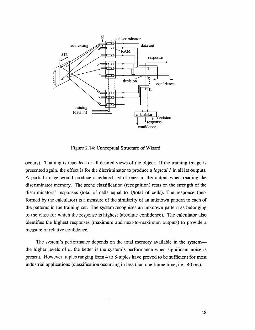
/ discriminator
addressing data outR AM
512 .response
512 decision !
confidence
training (data in) calculator
decision1 response
confidence
Figure 2.14: Conceptual Structure of Wisard
occurs). Training is repeated for all desired views of the object. If the training image is presented again, the effect is for the discriminator to produce a logical 1 in all its outputs. A partial image would produce a reduced set of ones in the output when reading the discriminator memory. The scene classification (recognition) rests on the strength of the discriminators’ responses (total of cells equal to 1/total of cells). The response (performed by the calculator) is a measure of the similarity of an unknown pattern to each of the patterns in the training set. The system recognises an unknown pattern as belonging to the class for which the response is highest (absolute confidence). The calculator also identifies the highest responses (maximum and next-to-maximum outputs) to provide a measure of relative confidence.
The system’s performance depends on the total memory available in the system— the higher levels of n, the better is the system’s performance when significant noise is
present. However, tuples ranging from 4 to 8-tuples have proved to be sufficient for most industrial applications (classification occurring in less than one frame time, i.e., 40 ms).
48

2.2.3.2. Analog Implementations
The first and simplest idea for implementing analog neural networks uses resistors as synapses and amplifiers as the cell body to perform the threshold function. The circuit of Figure 2.15a is a straightforward electronic implementation of the weighted summation function s = TfJL S.W - 0J70.
Input(dendrites)
Resistors(synapses)
Amplifier (cell body)
Output
(axon)u t
A1
output lines
A2 A3 A4
ne
A3 A4A1 A2
(a) Electronic Neuron (b) Interconnected Neurons
Figure 2.15: Analog Neural Network
Wires replace the input structure (dendrites) and the output (axon). The value of each coupling resistor is given by Rij=l/wij. In the synapses, the output voltage (sj) of each neuron is converted to an input current /i;- =sj/Rij for another neuron i.
Figure 2.15b illustrates a neural network as a crossbar representation that uses these electronic neurons. In the analog connection matrix, outputs (vertical lines) A1-A4 are
connected through resistors to the horizontal summing wires, which contain the weighted sum of the output signals of other PEs. Inverted input lines are provided when both positive and negative values are required.
For many neural network applications, however, it is necessary to change the
synapses values52. To implement programmable connections, a synapse circuit replaces
resistors. The circuit employs transistors operating in their ohmic (resistive) regime to implement different synaptic strengths.
Many groups are working on analog special-purpose neural chips2 ’5®’12 . Some
network implementations include hybrid digital-analog devices in which the synaptic
49

weights are typically stored in RAM memories87. Denker, Jackel and their colleagues at AT&T Bell Labs have designed a number of neural net chips that include: a hybrid digital/analog programmable connection matrix, comprising 54 fully interconnected neurons; an analog connection matrix with adjustable connection strengths, used for learning when small adjustments are required; and a digital pipelined best-match chip, a digital classifier-51 * 8> 7^
At the California Institute of Technology (Caltech), a team led by Mead, has also pioneered neural chips. Their first prototype was an associative memory chip containing 22 amplifiers and a full interconnection matrix that consumes 462 programmable interconnection elements. To implement large arrays, they have reduced power consumption by keeping the MOS transistors in a subthreshold regime of operation114. Comprehensive studies of biologically inspired analog VLSI neural networks are presented in his book83.
Commercial custom chips have been designed to implement analog networks. Mitsubishi Electric has developed one of the fastest and largest scale learning neurochips22. The chip contains 336 neuron units and 28,000 connections. Synapses weights are expressed by the amount of electric charge in capacitors, and learning takes place through changes in their charge. The execution speed is claimed to be 1 TCPS (1012 connections per second) during recall and 28 GCPS (109 CPS) during learning.
Intel and Nestor Inc. have worked in a joint project to fabricate the N1000, a neurochip based on Intel’s EEPROM memory, which will integrate over 1000 neurons. N1000 will be an advanced version of Intel’s first neurochip, N64 (80170NX). These chips implement (externally) modifiable synapses using floating gate non-volatile memory technology43. The use of an analog charge on a floating gate to replace digital memory
was proposed by Alspector18. Later, Intel’s technological development group proposed a new floating gate synapse which operates differentially. Differential floating gates provided: stable operation in presence of power supply and temperature changes (which occur between the time a network is trained and the time it processes information); and
benefits for the multiply function such as improved linearity and four quadrant multiply (synapse circuit producing correct signs and product for positive and negative, inputs and stored weights)43. This project, called ETANN, led to the Intel’s N64 chip. The chip uses 10240 floating gate synapse cells to implement 8192 synapses which fully interconnect 64 neurons and connect the 64 neurons to each of 64 inputs. Performance is of the order of 1010 low precision— 4 bit— multiplications per second.
50

2.3. Summary
There are two important aspects in the VLSI design of parallel computers: one is the node architectural complexity of each processing unit; the other is the system structural architecture of the parallel units. The corresponding aspects in the neural network architecture are respectively neural processing units and the synaptic connectivity pattern. Here we analyse this correspondence, discussing the examples of neurocomputers architectures seen in this chapter.
2.3.1. System Architecture
In this section we use four design attributes— communication structure, computation model, design approach, and implementation technology— for the analysis of neuro- computers’ system architectures.
COMMUNICATION STRUCTURE
The communication structure denotes the interconnection topology of physical processors (e.g., bus, ring, hypercube, etc.), and the width of physical links (i.e., parallel or serial). The interconnection topology affects parallelism, performance and the cost of a neurocomputer in different ways. Parallelism relies on packing density and regular communication structures to support architectural expandability. Performance is directly affected by the network communication diameter (or inter-node path length) and by the width of the links12. Cost escalates with extra coupling interfaces, special line drivers, global synchronisation circuits and external controllers. Several interconnection network topologies have been proposed12. The most popular are: the shared bus, the linear array (or ring), the grid, and the hyper cube.
With regard to parallelism, high performance interconnection plans, such as the hypercube («-cube) and even the grid, do not scale well in integrated circuits. The reason for this is the spatial diversity of links and the parallelism of bits in each link. Integrating more processors per chip results in increasing the number of pins (up to the package pin
limit) or narrowing communication links. In the case of the hypercube, both hardware configuration and communication software of each node need also to be altered if a hypercube needs to be expanded at some future time69.
On the other hand, the bus and the linear array exhibit an unlimited clustering capability at chip level thus, allowing easy expansion when chips are implemented with
51

denser technology. In both cases, the coupling of the processing devices is simple, yielding to a scalable system architecture. However, bus-based systems entail more complex hardware for bus allocation and arbitration. Also, a single bus can not support a large number of processors. Heavy loading demands special drivers and subject the processors to long waits, slowing the whole system. Furthermore, no matter how robust the arbitration protocol and bus drivers, only one "talker" can exist at a time. Multiple-buses (segmentation for parallelism) need selective repeaters, and do not scale well54.
As a point-to-point topology, the ring implements high speed unidirectional links. System size and clock rate are decoupled. Signal handshake and communication protocol are greatly simplified because there is always one driver and one receiver, at opposite ends of the link. Large networks can be implemented by either increasing the size of a ring, or by utilising rings as building blocks.
Both, the linear array and bus topologies are considered to be the best candidates for large scale neural networks and wafer scale integration3®. Some wafer scale designs have already been proposed65,99*135,136.
When considering performance, the hypercube, followed by the grid117,118, appear to be more efficient than the other interconnection topologies (in particular if a message is to be sent to distant processors). However, taking into account serial links and the control overhead to route messages, the performance of the hypercube decreases. For instance, in the Connection Machine (which has both grid and hypercube network interconnections), a typical message of 32 bits with a 16-bit address takes about an order of magnitude longer to be sent using the hypercube network than an equivalently sized message using the NEWS grid105. The fact that 32-bit messages have to be serialised to be
transmitted degrades performance drastically. In a simulation study, Delgado has shown
that message delays increased almost two orders of magnitude when the width of the links in a hypercube is varied from 32 bits to 1 bit33.
Mixed topologies, combined with a proper mapping of multi-layer networks, can deliver higher performance— sometimes at a higher cost (e.g., the Connection Machine).
COMPUTATION MODEL
This attribute indicates how processors are organised to compute the neural algorithms, i.e., MIMD, SIMD, SISD, systolic architecture, etc. Examples of neurocomputers
cover all three categories. The SISD (single instruction single data) defines conventional serial computers supporting neural networks. These neurocomputers constitute a cost-
52

effective and flexible solution for applications in which time is not crucial. Incorporat
ing accelerator co-processor boards increases their general performance.
SIMD architectures typically employ a large array of very simple processing elements which operate in lock-step synchronism. These implementations may require considerable amount of external hardware. Frequently, one sequence controller is necessary for each array of processors executing concurrently different neural network layers. The Connection Machine, for instance, requires for every set of data processors, a sequencer which breaks down high level instructions (Paris language) into a sequence of low-level processor and memory operations4. This class of neurocomputers is generally versatile and offer high speed. In cases where only a limited set of instructions is provided, the degree of flexibility of SIMD neurocomputers tend to be relatively small (e.g. CNAPS).
MIMD neurocomputers are asynchronous, fully programmable machines, characterised by decentralised hardware control. Communication between processors is by message passing or shared memory. MIMD neurocomputers are versatile and provide a high-level framework for the development of neural network models and applications. The appeal for MIMD neurocomputers is in view of asynchronous operation and support for neural network description languages. Transputer-based systems such as the Meiko Computing Surface and TRW Mark III co-processor are typical examples.
In all these categories, the neurocomputer is usually assisted (at the system architecture level) by a host machine, be it a microcomputer, a transputer or a workstation, which performs network initialisation, control, and sometimes part of the neural computations.
DESIGN APPROACH
Design approaches include fully implemented neurocomputers and virtual neurocomputers. Fully implemented neurocomputers have dedicated hardware for each neuron processing element and synapse connection they implement. Virtual neurocomputers, on the other hand, map a neural network across the available processors and physical connections using time multiplexing techniques. Fully implemented neurocomputers tend to use simpler processors and improve performance by real parallelism. In employing simpler units, virtual processing is not always possible due to the limited amount of local memory associated with each processor. Nevertheless, virtual processing is desirable to attain the full capacity of hardware implemented resources; a trade-off has to be made.
One argument against fully implemented neurocomputers is the low efficiency of large processor arrays when executing multi-layers neural networks61. In these neural
53

networks, neuron elements of a layer must wait for the output from the preceding or succeeding layer to perform their tasks. As matter of fact, if the number of neurons in different layers varies, then the time required to compute the largest layer prevails. However, for continuous operation (input patterns appearing regularly or a pattern being classified several times), fully implemented neurocomputers benefit from parallel processing, and deliver higher performance.
Most of the commercial accelerator co-processors use virtual processing extensively over a small number of processor units (e.g., the TRW Mark III uses up to 15 processors)^1. Novel products such as the CNAPS, employ a relatively larger number of processors (256 PN processors), and also allow for them to be arranged in separated segments, to cope with multi-layers networks5-5.
IMPLEMENTATION TECHNOLOGY
This typically involves electronic analog, and digital hardware. With regard to implementation technology, the important issue for neurocomputer system architectures is the device coupling interface. Hardware interfacing in neurocomputers occurs in various levels: chip, board, network segment, and system levels. The problems with analog implementations relate to electrical instability and difficulties in matching off-chip (and off-board) impedance and capacitance. To simplify system integration and interfacing, designers adopt digital input/output, converting signals properly for internal analog processing. This approach combines the advantages of high density of analog neurons with the easy interfacing of digital systems27. Additionally, problems such fluctuations in parasitics and noise, appear to limit the number of chips in analog networks. Designers at Mitsubishi experienced such a problem during the project of an analog neural network chip22. In fact, the high density of analog circuits favours more the implementations of single chip neural networks such as the one developed at AT&T Bell Laboratories, New Jersey27.
Digital implementations benefit from reliable and supported interfaces such as serial and parallel ports, VME bus, Ethernet LANs, and so on. These standard communication
vehicles facilitate system integration and promote mixed topologies. Several examples of
neurocomputers adopt a heterogeneous system architecture. For instance, the Connection Machine integrates grids of processing nodes in hypercube topology with I/O interfaces to diverse external systems. The Meiko Computing Surface allows different topologies through a chip (the Message Link Switch), which configures the system architecture^.
54

2.3.2. Node Architecture
The complexity of the node architecture determines how efficient it can be to cope with neural processing and to attend the design issues of high parallelism, performance and flexibility. The choice of node architectures range from primitive neural processors such as the ETANN node, to complete microcomputer systems such as the NETSIM. Here, we assess these architectures according to the attributes of capacity, accuracy, and generality.
CAPACITY
Capacity refers to the size of the neural network and/or the number of different neural networks that can be implemented (represented and stored) in a neurocomputer system. Capacity is determined by the node implemented memory, needed to store weights, lookup tables, and other values. The total required capacity for a node is relatively low but varies for each application. For instance, using virtual interconnections, a weight table may contain an entry for each pair weight/virtual-interconnection. Thus, a fully-interconnected Hopfield neural network^7 with 256 neurons (8-bit weights), requires only 256x16-bit words of RAM in each node. For lookup tables, if the eight most significant bits of the weighted sum are used to select one of 256 possible outputs, a 1 Kbyte RAM suffices for a lookup table for up to four different transfer functions.
Co-processor boards and conventional computers are less influenced by memory requirements, since each node can implement large amounts of external memory, only limited by the microprocessor address space (4G words for 32-bit microprocessors). Medium-grained parallel systems (up to 256 nodes) such as the Computing Surface and CNAPS have a small local memory (usually 4 Kbytes) at each node, and a large external memory, global to the array. Fine-grained parallel systems rely mostly on the node’s local memory. In these systems, access to a larger external memory is difficulted by the interconnection topology of the processing nodes and the large number of them. For
example: in the Connection Machine each processor has 8 Kbytes while the Hitachi WSI implements just 64xl8-bit words for each node.
ACCURACY
Accuracy means the capability of a neurocomputer to represent quantities or express results, adequate to neural networks. Most of the simulations and theoretical predictions for neural network algorithms consider that operands such as synaptic weights are of the real type using floating point notation. For VLSI implementations, architecture
55

complexity is greatly reduced when limited-range integer-type coefficients are used. The question is, which numerical accuracy is required on the operands for the different neural models? Accuracy varies considerably depending upon the type of network being implemented. Binary networks such as the Hopfield one, are typically more tolerant to lower accuracy than networks such as the Backpropagation and Counterpropagation61. In general, accuracy is more important during learning than it is during recall— the number of bits representing weights affects learning time and may not be sufficient to achieve convergence. Researchers have been trying to set accuracy requirements for neural networks applying different methods. Alippi, used three theorems to show the relationship between convergence of learning phase of Backpropagation algorithm and neural values16’17. The first theorem reduces the complexity of the activation function of the neuron’s output layer by stating that a simple step function performs as well as the complex activation functions such as sigmoid and thermodynamic functions. The second theorem sets the precision requirements for the weights as a function of the learning rate (tj) and the output error (e). The third theorem shows a linear relation between weight size, learning rate, number of steps of the learning phase, and the activation function parameters. Nigri^4 has performed extensive simulations using the Backpropagation
neural network to recognise numerical characters from 0 to 9. His studies have shown that accuracy depends on the algorithm parameters, rj and e—for greater rj and e less bits are required to represent weights. A minimum of 10 bits for weights has been reported. Using theoretical arguments and numerical simulations, Duranton proposes that 16 bits precision on synapse weights should yield the same accuracy as with floating point variables, for Hopfield and Multilayered networks35. Sirat assessed the precision requirements on input data for single-layer Perceptron and Backpropagation, and proposed two
alternative approaches which achieve fast learning for any accuracy113: the first consists
of a simple preprocessing of the input data; the second adopts variants of the models which use adaptive learning parameters.
Most of the neural VLSI chips employ integer arithmetic operations and represent neural quantities with diverse sizes. Accuracy is a major problem in analog designs, being limited only by implementation size in digital processors. Analog neural VLSI
chips have employed as little as 6 bits for weights and 3 bits for inputs27, while digital neural processors implement a minimum of 8 bits (usually 16 bits) for all network values.
GENERALITY
The generality of a neurocomputer determines the degree of flexibility to execute (train and recall) different neural network models and to support neural software.
56

Generality tends to conflict with parallelism and performance and it is relevant to the class of general-purpose neurocomputers. Special-purpose neurocomputers, tied to specific applications, will typically be trained once (or periodically) and this can be achieved off-site using external supporting hardware or a general-purpose neurocomputer. General-purpose neurocomputers are expected to support the computation of weight changes (learning) and to assist neural network environments.
To date, most of the analog ICs use off-chip learning support29. Some of them
implement programmable synapses, which means that weights (calculated externally) can be electrically or optically loaded11. Analog in situ learning has already been achieved using techniques such as the capacitive control of synaptic weights22,44. The first steps towards programmable analog neural network processors is observed in designs such as ANNA (Analog Neural Network Arithmetic and logic unit). This chip implements three instructions, CALC, SHIFT, and STORE, to perform general computation27.
Neurocomputer architecture based on programmable processors, such as accelerator co-processors and conventional computers, are certainly the most flexible systems. Accelerator co-processor boards (e.g. TRW Mark III)7-5 typically employ nodes as being complete microcomputer systems (including a floating point processor and a large memory), and are not suitable to implement highly parallel architectures. Conventional parallel computers, based on microprocessors such as the transputer, achieve a better compromise between flexibility and parallelism. Transputers, as well as conventional RISC processors, reevaluate architecture trade-offs in the context of VLSI capabilities. However, the designers of microprocessors such as the Sparc and the Transputer created a highly optimised design to support general-purpose, multiprocessing computing systems. According to neural network processing requirements, a simpler, transputer-like node architecture, can attain a rational balance between parallelism and flexibility.
57
Chapter 3
Neural-RISC System Architecture
This chapter describes the architectural framework for the Neural-RISC system architecture. This includes: the system s components, topology and configuration, and its mode of operation.
3.1. Architectural Framework
There are three major components in the system architecture, as depicted in Figure 3.1: the Neural-RISC processor array {Neural-RISC array), the Multi-ring Interconnect (MI) module, and the Host, The Neural-RISC array performs the computation routines dedicated to low-level neural network functions such as weighted sum function, threshold function and weight updating, and network supervising operations to monitor, modify, and control execution of a neural network. The Multi-ring Interconnect Module handles the input/output between arrays in a cluster, and between the cluster and the host. It acts on demand, switching packets between links that are currently requesting service. The host supplies data to and receives results from the arrays and supports neural network development. The user supplies details about network configuration and topology, neural node activation and connection update rules, using a neural network description language; a compiler handles the details of code generation and partitioning; the host then downloads a specific code which programs each Neural-RISC processor. In addition, the host executes parts of the application programs that are not mapped onto the Neural-RISC array. For instance, the host may support a neural network development environment. Typically such environments consist of a set of general graphic tools and an algorithm library (e.g. Pygmalion)21.
3.1.1. System Configuration
The Neural-RISC array is a linear array of identical processors connected in a ring
topology (see Figure 3.1). Rings may be constructed from an arbitrary number of
Neural-RISC processors and may have different sizes. Each ring ends up in a MI module to enable connection between rings. Messages in the form of packets flow through the
58

RNeural-RISC processors
Neural-RISC array
HOST «*
Multi-ringInterconnect
Module
Figure 3.1: Neural-RISC System Architecture Overview
array using two alternative communication channels (R and L). Channels are completely independent, with opposite directions (right and left) to shorten the distance between two communicating processors. Each channel is implemented across the array by point-to- point, unidirectional (16-bit) links. Two standard handshaking signals control data strobing on each link. Since a dual channel is employed, a processor can send and receive messages simultaneously. Communication through the ring involves a simple algorithm
for broadcasting and routing packets. The transport of packets between processors is synchronous, but the network as a whole performs asynchronously. The consequence of this is that multiple transfers are supported on different parts of the network at the same
time.
The Multi-ring Interconnect module is an autonomous unit with a standard microprocessor implementing a set of parallel I/O ports. Parallel ports are physically and logically compatible with the interprocessor links, in a number sufficient to attend the
connected rings. Additional parallel interfaces provide means to connect a MI module to other MI modules or to the host. The MI module contains memory buffers and a routing
59

table to support inter-ring and inter-system message passing. The routing table, which is loaded and updated by the host, maps processor network addresses to ring ports that lead to the addressed nodes.
The host functions as the master controller of the Neural-RISC system. Its design is outside the scope of this thesis. Typically, it would consist of a workstation which provides an operating system environment such as Unix, for running application programs. Thousands of processors, combined in few boards, can be embedded in a workstation, using the expansion slots of industry standard host machines. Alternatively, a larger number of processors can be integrated into a neurocomputer server that resides on a standard local area network.
The decomposition of the system in such a modular way provides the designer with a considerable level of flexibility when constructing and reconfiguring neurocomputer systems. In addition, the provision of programmable clusters of rings helps the programmer or researcher to implement various neural network algorithms independently, or to simulate a very large neural network application using all available clusters. The ability to integrate large numbers of processing elements without incurring excessive communication overheads makes the system appropriate for neural computing.
3.1.2. Expanded Systems
The neurocomputer architecture is designed to be expanded into larger systems with minimum disruption of the existing setup, to match performance and application requirements. The scalability of the Neural-RISC system architecture allows constructing neurocomputers ranging in size from few processors to thousands of processors (Figure 3.2). Theoretically, the system can be scaled up to 65,536 nodes although, in practice, the use
of selective broadcast addresses may limit the size of the system. Systems can adopt a number of configurations, capable of meeting a variety of user requirements. For instance, clusters of rings can be arranged in different point-to-point topologies such as ring, mesh, cube, tree, etc. An optimum system size and configuration can be established by three alternative methods:
1) increasing the size of the ring,2) utilising more rings,3) employing multiple clusters of rings.
60

N eu ra l-R IS C C h ip
C lu ster
Figure 3.2: Scalable Communication System
The size of the ring grows with the number of integrated processors in a chip, and with the number of chips. This method is attractive for low-cost implementations due to the simplified coupling of the Neural-RISC chips. A ring may contain any number of processors: large rings simplify system integration, while short rings reduce the average
distance messages must travel in the network.
Rings can be utilised as the fundamental building block for very large systems. The number of rings in a cluster is only limited by the I/O capacity of the MI module. In general, many rings per cluster favours system performance (if the I/O capacity of the
61

MI module does not overwhelm communication throughput) and reduces implementation cost.
Multiple clusters of rings, each containing a MI module, can be employed without affecting communication performance substantially. These subsystems may be independent, running different applications, or act concurrently to execute a large neural network.
A salient characteristic of the Neural-RISC system architecture is its ability to expand into larger systems, virtually, with no loss of performance. In multicomputer systems, performance is largely influenced by the interconnection network, i.e, the interconnection scheme that ties all the processors together. In this respect, one of the most important evaluative measures of the interconnection network is the average distance— the number of processors (or links) a message must cross (in average), to reach the destination node. The average distance (Ad), as defined by Agrawal12, is given by the formula:
where N is the total number of processors, Nd is the number of processors at a distance d links away, and r is the maximum distance (diameter) between any two pairs of processor nodes.
For a bi-directional ring, with N processor nodes, the average distance is found to be (N + l)/4 , where N is odd. (The expression for N even can also be obtained, but the relations are not so neat)12. Using this result to calculate the average distance for a Neural- RISC cluster (AdNR), composed of N processors, evenly distributed across R rings (R>1), we obtain:
AdNR=(N +R )l2R
(Note: The presence of the MI module grants a single vertical communication step between any pair of rings. Thus, in a Neural-RISC cluster the network diameter is N/R, which corresponds to the diameter of a ring with (2N/R + 1) nodes).
For a meaningful examination of the effect that the number of rings have on the system’s performance, let us plot the curves of average distance versus cluster size (i.e., the number of nodes) for various cluster configurations. Figure 3.3 shows the curves for an adequate set of cluster configurations (8 to 128 rings per cluster).
62

Average Distance
3008 Rings
250 |16 Rings
-32 Rings200
J64 Rings150
128 Rings100
2 4 8 16 32 64 128 256 512 1K 2K 4KNumber of Nodes
Figure 3.3: Average Distance for Different Cluster Configurations
In a Neural-RISC cluster, the dependency of the average distance on the number of
processors N is reduced by a factor o f 2R. Thus, for the same network size, the average
delay decreases as the number of rings increases. Consequently, a system based on a
higher number of rings achieves better response time. For instance, using clusters with
128 rings, the average distance is under 33 links for systems with up 4096 processors.
The average distance of a complete system will depend on the system topology (i.e.,
ring, mesh, cube, etc.), that physically interconnects the Neural-RISC clusters. However,
for a cluster-based architecture such as the Neural-RISC, the relevant metric of com m un
ication performance is the performance of a cluster, since mapping strategies try to
minimise the inter-cluster traffic of messages.
3.1.3. Message-Routing System
Neural-RISC processors communicate with each other by sending and receiving
messages. The communication system is essentially a packet delivery system, where a
packet constitutes a complete message. Packets are o f user-programmable length: 32-
word packets are used for the system initialisation; after this phase, the user can set the
63

packets’ length according to the application requirements and to the size of I/O buffers.The structure of a message packet is depicted in Figure 3.4. Each packet consists of threeinformation fields:
NETWORK IDENTIFIER -a single word containing a 16-bit network address, whichindicates the recipient node(s) within the network.
LINK IDENTIFIER -a single word containing a 16-bit virtual link number,which identifies the target input link within the processor node.
DATA FIELD -a sequence of n-2 (16-bit) words of data.
WordO Network Identifier a network address: from 0 to 65535Word 1 Link Identifier a virtual link number: from 0 to 65535Word 2-/i Data Field a sequence of n-2 words.
Figure 3.4: Message Packet Format
Packets are transmitted a word at a time, with the network identifier transmitted first. In the Neural-RISC arrays, the intended destination of each packet is determined on fly and the remainder of the packet is clocked (i.e., forwarded) without interruption by the processor nodes. Contrary to the store-and-forward procedure, this method provides a good match for the linear array topology since message packets have a single route when crossing intermediate nodes. Overall, this method reduces the packets’ transmission time, thus contributing to improve communication performance47.
Next, we give details on the role of network identifier and link identifier fields.
The Network Identifier
The 16-bit Network Identifier enables up to 64K unique network addresses. Network addressing is based solely on the network identifier. The network addressing
scheme is flexible, allowing the user to set it according to applications. The system supports two addressing modes—direct mode and cast mode— and divides the network address space into six segments:
64

D irect mode
Node: points to a specific processor as the destination node.
Host: points to the host as the recipient of that message.
Ml Module: points to a specific MI module as the recipient of that message.
Cast mode
Layer: selects a cast group of processor nodes belonging to the same neural network layer as destination nodes.
Cluster: selects a cast group of processors nodes that belong to a cluster in a particular neural network layer.
Broadcast: selects all processors in the network to receive an identical copy of a message.
(Note: The terms cluster and layer used in this section, refer to structures present in some neural networks models and not to architectural features).
Each address segment consumes part of the network address space. The use of group addressing reduces the number of possible processor node addresses in favour of low network traffic. The size of the address space S is given by the sum of segments’ sizes:
S = UNode + ULayer + UCluster + UBroadcast (=1) + UHost + UMl = 64K
Except for the broadcast address, which is hardware built-in to the Neural-RISC
processors (all l ’s address), all other addresses are essentially user-programmable. For instance, segments can be associated with sequential addresses, covering part of the address space, or can also coincide. When addresses coincide, an input arbiter at the Neural-RISC processor determines the addressing mode based on a prefixed order of priority. The arbiter checks if it is: first a node address; second the broadcast address; third a layer address; and finally a cluster address. Thus, if in a processor node, the layer
and node addresses are the same, packets sent to this address will always be treated as being directed to that processor node only (refer to section 4.2.1.3 for details).
Processor nodes can be reached either through direct mode or cast mode addresses. Packets sent to cast groups will be received and forwarded by the selected processor
65

nodes, and routed to appropriate rings and clusters of rings by the MI modules.
The network addressing scheme comes into effect after initialisation and can be changed dynamically during operation by using control commands (see section 3.2.2). The scheme is flexible, providing independence between network address and processor’s physical location. For instance, a neural network layer may correspond to a ring (Figure 3.5), or can be spread across several rings. Processing elements in different neural network layers (or clusters) communicate by sending a single packet to the specific layer (or cluster), thus reducing substantially the traffic of packets in the network.
A cluster of rings may execute one or many neural network algorithms, according to the size of each application. The fact that a Neural-RISC processor can respond to four different network addresses (i.e., node, layer, cluster, and broadcast), allows implementing essentially any conventional neural network (Figure 3.5), or arranging different algorithms in the same neurocomputer system. Additionally, the system can support virtual processing, by mapping processing elements across the physical processors.
Layer 1
L a ye r2
Cluster
Layer n
VirtualPE
Virtual- P EVirtual
J - _RE_ j
□Neural-RISC NeuronProcessor Element
VirtualConnection
Figure 3.5: Mapping of Neural Networks
66

The Link Identifier
The role of this field is to establish virtual links between communicating system’s elements. Virtual links provide a "virtual" connection between elements that are not physically connected. They can be used for different application purposes, where each application is associated with a range of virtual link numbers. The range identifies the packet mode, i.e., it specifies the action to be taken by a processor, a MI module, or the host on reception of a message packet. A number of different packets modes have been devised.
Virtual Interconnection Mode— to support virtual interconnections between neural processing nodes. In this mode the link identifier is used to search the weight table for the corresponding entry (virtual-link/weight).
Virtual Processing Mode— to support a number of virtual processing elements per processor. In this mode the link identifier serves to distinguish between processing elements that share the same network address (a unique set of virtual link numbers is associated with each virtual processing element).
Direct Address— to provide direct addressing in remote processors. In this case the sender uses the link identifier to specify a physical address within the processor’s memory, for read and write operations.
Control—to support network control and monitoring operations during neural network simulations. In this mode, preassigned virtual links are used to command the execution of routines, which are resident in the processor nodes and in the MI modules.
The 16-bit link identifier can support a virtual link address space of up 64K virtual link numbers per system element. Some virtual link numbers however are considered global for specific groups of nodes or for the network. This is because cast addressing
modes produce identical copies of a packet to several nodes. For example, a broadcast packet, carrying virtual link #10, can be issued by the host instructing all processors to change the learning rate for the next iteration of the neural network. In this case, all processors will have link number 10 as a global link, associated with a control routine.
3.1.4. Routing Algorithm
The routing algorithm is extremely simple and can be adapted to fit specific applications. It is basically executed by the Neural-RISC processors and the MI modules. When
67
a packet arrives at a processor, the network identifier is compared with its various network addresses (i.e., node, layer, cluster, and broadcast). The processor node then assumes one of three alternatives:
• Receive the packet if its network identifier matches its node address.
• Receive & forward the packet if its network identifier matches the processor’s layer, cluster, or the broadcast addresses.
• Forward the packet if its network identifier does not match any internal address.
To transmit a packet, the processor uses the size of the ring it belongs, to determine the channel (R or L), that leads to the shortest path to reach the destination node. (This path can pass or not through the MI module). Cast-mode packets are sent in both directions simultaneously, generating two copies of the same packet, that will reach the MI module. (The MI module controls the spreading of packets). This procedure guarantees that one (and only one) copy of a cast-mode packets will reach the addressed processors in the same ring.
The MI modules execute part of the routing algorithm for supporting inter-ring and inter-cluster communication. Routing through a MI module involves a single vertical step towards the destination processors, regardless which rings the processors involved in the communication are located. At a MI module, routing is based on the store-and- forward procedure. Since incoming cast-mode packets are supposedly addressed to different rings and clusters, they can be forwarded through alternative routes, and therefore, need to be stored when selected paths are busy. The use of this procedure by the MI modules releases the coupling between communicating processor nodes in different rings and clusters thus, favouring system’s performance. Routing at MI modules involves: passing incoming packets onto destination rings and clusters according to the routing table; and controlling the spread out of cast-mode packets in the multi-ring system (cluster). The routing table has a straightforward mapping of network addresses to rings, where each ring is represented by two I/O port numbers, according to the channel they
give access (R or L). The channel that leads to the shortest distance to access the destination nodes, is used by the host to create the table.
The spread out of cast-mode packets is controlled in two steps: first, by forwarding
copies of these packets to selected rings; and second, by discarding packets that have already circulated. To do that, the MI module stores packets temporarily, and creates dynamically a control table which associates ring port numbers to cast-mode packets. Each time a cast-mode packet comes in, the MI module compares its contents against the
68

ones indicated by the control table and takes proper action, i.e, it discards or forwards that packet.
3.1.5. Resources Management
A communication system can be viewed as a set of resources shared by a collection of processes that exchange information with each other. As such, a communication system is susceptible to deadlocks. A situation can occur in which two or more processes
are waiting for physical resources to be released by each other. It is then possible for these processes to block each other’s progress indefinitely. Several different conditions can lead to deadlocks. The most common types of deadlocks in communication systems are: protocol deadlock and buffer deadlock119. Protocol deadlocks result when two or more tasks are waiting on each other for some type of control message and no further movement of messages can occur. Buffer deadlocks can occur when two or more nodes have no free buffers and each node is waiting for some other node to release a buffer.
In the Neural-RISC architecture, the inherent simplicity of the communication structure and routing algorithm, allows us to give a straightforward demonstration of how deadlock is prevented.
Protocol deadlocks are not actually significant to the Neural-RISC architecture, since there is no communication protocol beyond the link interface level. Communication links are unidirectional, and as so, do not involve contention for access. A link interconnecting two neighbour processors is controlled by a simple protocol, executed by a pair of handshaking signals: a request-to-send and a clear-to-send (strobe) signal. A
similar protocol is widely used in computer interfaces (RS232-C) and is known to be free of deadlocks.
The Neural-RISC array is free of buffer deadlocks due to its dual communication structure. Communication between any pair of processors use distinct channels, one to
transmit and another to receive. The processor provides separated input and output buffers, supporting each channel. Channels are completely independent, and the routing algorithm guarantees that packets can not loop back to the sender node. Therefore, receiving a packet does not depend on releasing a buffer occupied by a packet needing to proceed to another processor. This scheme prevents deadlocks that result from the mutual wait among processors. The diagram of Figure 3.6 illustrates the communication structure.
69

forw ardforw ard Channel R- > ■
BuffersBuffers
Channel L< -
forw ard forw ard
Node i Node i+1
Figure 3.6: Communication Structure of Neural-RISC nodes
In communication systems, network congestion can ultimately lead to a deadlock if proper flow control is not present119. This type of deadlock is typical in systems that employ the store-and-forward procedure. The MI modules employ such procedure and deadlock-free operations rely on the large size of I/O buffers available and on the use of alternative routes in each ring (channels R and L) to deliver a packet. In the Neural- RISC array, packet words are forwarded as they are received by intermediate nodes thus, input buffers are not required for holding packets in transit towards another processor. Therefore, a node processor never locks up in consequence of heavy traffic loads. (This phenomenon is known as store-and-forward lockup.)13 However, it is possible for a channel to become blocked if one or more processors have no buffers available to receive packets addressed to them. In this situation, no movement of packets can take place until some buffer is freed in these processor nodes (namely, packets being read by
the processors). To avoid blocked channels and to prevent the possibility of process starvation, the system must rely on the fairness of processes running on node processors, which should make adequate use of the available flow control mechanisms.
At the processor level, flow control is based on polling and interrupts. To receive packets, a processor must poll a packet counter whenever it is convenient in order to
optimise its internal loads; an interrupt is generated by the communication unit when a
input queue is full. The simple mechanisms of polling and interrupts are suited for neural network models, on the assumption that these algorithms are more disciplined in respect to input and output.
70

3.2. System Operation
3.2.1. Initialisation
System initialisation involves two phases: loading and synchronisation. Downloading simple programs into each Neural-RISC processor and routing tables into MI modules, configures the neurocomputer. Synchronisation avoids network activity before
loading is complete.
Loading consists of a configuration packet and a number of data packets. It is conducted by the host, and takes place just after general reset, when processors execute the resident boot-strapping code. During loading, the host transfers the routing tables to MI modules and then the configuration packets to all system’s elements. The initial operations configure: node, layer, and cluster addresses equal to zero, and length of packets equal to 32, to all processors and MI modules. In this state, processors can execute the routing algorithm and wait for incoming packets. The configuration packet (Figure 3.7) contains the processor’s network addresses and the first loading data words. Individual versions of this packet are addressed to each processor, starting from an end of each ring.
WordO Network Identifier an all 0’s network addressWord 1 Node Address the processor’s configuration node addressWord 2 Layer Address the processor’s configuration layer addressWord 3 Cluster Address the processor’s configuration cluster addressWord 4 Load Counting total number of data wordsWord 5 Loading Address memory starting address for loading dataWord 6-31 Data Words the sequence of the first 26 (16-bit) data words
Figure 3.7: Configuration Packet Format
On receiving the first packet, processors assume their unique identification in the network and wait for data packets. A number of data packets are then sent to each processor to complete the specified counting. Each subsequent data packet has the format shown in Figure 3.8.
Data packets can be sent individually to each processor, or to groups of them, using cast-mode packets. This process can speed up the loading phase when processors have identical code segments. Since data packets carry a memory starting address, they can be sent through both channels, in any sequence.
71

Word 0 Network Identifier any valid network addressWord 1 Loading Address memory starting address for loading dataWord 2-31 Data Words a sequence of 30 (16-bit) data words
Figure 3.8: Data Packet Format
Synchronisation is obtained by means of an external signal (SYNC), common to all processors. This signal interrupts the Neural-RISC processors, commanding them to execute the newly loaded code. This way, network operation only starts after all processors have been properly configured and loaded.
3.2.2. Control & Monitoring
The system provides support for implementing a number of user-defined operations to control and monitor the network. These operations are typically defined at the environment programming system level123, and are initiated by the host.
Control and monitoring operations are implemented by means of commands and responses in the form of packets. Control packets, invoking designated virtual links are sent to individual processors or groups of them. Each virtual link number points to a specific routine in the processor’s memory, that executes the associated operation. The same virtual link can be used to return the information requested when monitoring the processor’s activity. The general format of control packets is shown in Figure 3.9.
WordO Network Identifier any valid network addressWord 1 Control Link a virtual link associated with the control operation.Word 2-n Control Data a sequence of command parameters or network data.
Figure 3.9: Control Packet Format
To illustrate the functionality provided by control packets, we describe in Table 3.1 a set of possible commands to support the simulation of neural networks. Commands can have three different purposes:
Modification—to alter the neural network’s variables and topology, while the simulation is running, or to change the neurocomputer’s configuration.
72

M o n i to r in g — to e x a m in e sp e c if ic n etw o rk d a ta d u r in g e x e c u t io n .
E x e c u t io n — to start, s to p and halt the e x e c u t io n p h a se s o f th e n eu ra l n e tw o r k .
CO M M AND Operand Function Target NodesModification
SET learning rate set new learning rale groupm inimum error set new minimum error groupsynapse set weight value nodestate set neuron output node
ADD neuron add new neuron nodesynapse add new synapse node
DELETE neuron delete neuron nodesynapse delete synapse node
CH ANG E network address change processors' network addresses node or groupLOAD code load specific code node or group
M o n i t o r i n gPR O BE neuron gel neuron properties node or group
synapse get synapse properties nodeExecution
PH ASE learning start learning phase group or netrecall start recall phase group or net
STEP forward execute fo rw ard pass netbackward execute backw ard pass net
STO P network slop network netR ESUM E network continue net
Table 3.1: Control and Monitoring Commands
The implementation of the control and monitoring commands, presented in Table3.1, has implications on the design of the neural network description language compiler since, for instance, synapses may be deleted or created dynamically during network operation. The definite syntax and implementation of these commands are not part of this thesis. These issues will be addressed in a research project to be carried out as continuation of this work (refer to Chapter 8).
73
Chapter 4
Neural-RISC Node Architecture
This chapter presents the design philosophy of the Neural-RISC node architecture and describes its major components: the processor unit, communication unit and memory unit. It focuses on the organisation, architectural features and related operation.
The Neural-RISC is a primitive microprocessor whose design is optimised to the computation of neural network models. This self-contained microprocessor forms a complete building block to support a fine-grained, many nodes per chip, neurocomputer parallel architecture. The Neural-RISC node architecture, as shown in Figure 4.1, is
composed of three basic units:
• Processor Unit: a 16-bit RISC processor consisting of an execution unit, a timer, and an interrupt controller.
• Communication Unit: a double engine comprising four (high bandwidth) parallel links to implement communication channels in opposite directions, and support for two FIFO (programmable-size) buffers to transfer message packets.
• Local Memory: an instruction and data RAM block, the separated data RAM blocks that implement the communication unit I/O buffers, and a boot-strapping ROM.
The processor unit is based on a primitive RISC architecture. In its design we have followed the RISC philosophy for simplicity and efficiency10- . In contrast with conventional RISC architectures that adopt the load!storef design and a large register set, the Neural-RISC implements few registers and uses the onchip memory as the register file. Consequently, the execution model is memory-based, but all single-access instructions, including load and store, take only one cycle to execute. The processor adopts a very reduced instruction set but provides the necessary generality. To simplify the process of
t In the load/store or register-oriented architecture, operations are register-to-register, with only LOAD and STORE accessing memory. This way, most instructions can be made to execute in a single cycle62,103.
74
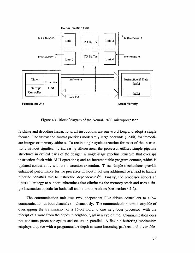
Communication Unit
LinklinDataO-15
Link3outDataO-15
Link 1 I/O Buffer
Link 3I/O Buffer
Link 2
Link 4
TimerExecution
Interrupt UnitController
Address Dus
AV
Link2outDataO-15
Link4inDataO-15
Data Bus
Instruction & DataRAM
ROM
Processing Unit Local Memory
Figure 4.1: Block Diagram of the Neural-RISC microprocessor
fetching and decoding instructions, all instructions are one-word long and adopt a single format. The instruction format provides moderately large operands (12-bit) for immediate integer or memory address. To retain single-cycle execution for most of the instructions without significantly increasing silicon area, the processor utilises simple pipeline structures in critical parts of the design: a single-stage pipeline structure that overlaps instruction fetch with ALU operations; and an incrementable program counter, which is
updated concurrently with the instruction execution. These simple mechanisms provide enhanced performance for the processor without involving additional overhead to handle pipeline penalties due to instruction dependencies62. Finally, the processor adopts an
unusual strategy to support subroutines that eliminates the memory stack and uses a single instruction opcode for both, call and return operations (see section 4.1.2).
The communication unit uses two independent PLA-driven controllers to allow communication in both channels simultaneously. The communication unit is capable of overlapping the transmission of a 16-bit word to one neighbour processor with the receipt of a word from the opposite neighbour, all in a cycle time. Communication does not consume processor cycles and occurs in parallel. A flexible buffering mechanism employs a queue with a programmable depth to store incoming packets, and a variable-
75

length buffer for outgoing packets. These features provide low-latency communication with adjacent processors and high-bandwidth data I/O across the processor array.
For the processor’s memory, we have made the fundamental decision to have no external memory, and gain in performance and in simplicity of system integration. The on-chip memory can supply 16 bits of data twice per clock cycle thus, allowing singlecycle execution for most of the instructions (including load and store), with minimum control circuitry. The maximum implementable memory for each processor (4Kx 16-bit) trades between the processor’s capacity and the parallelism of nodes integrated in a chip; the actual implemented memory for each node depends on the processing technology (this is discussed in Chapter 7).
Having given an overview of the design philosophy, we shall next outline the internal organisation of the node architecture by describing the processor, communication and memory units.
4.1. Processor Unit
4.1.1. Organisation
The logical structure of the processor unit is shown in Figure 4.2. The major functional components of the processor unit include: an Execution unit, a Timer, and an Interrupt Controller. The functional units communicate over two buses: bus A serves mainly as an address bus, while bus B is used as a data bus.
4.1.1.1. Execution Unit
The execution unit consists of a set of specialised registers and an arithmetic logic unit (ALU). The register set includes: the accumulator AX, the instruction pointer IP, the condition code register CC, the operand register OR, and the multiply auxiliary register MPX.
AX a 16-bit (shift) register, which is used as implicit (second) operand for most ofthe instructions.
IP a 16-bit register with its own (simplified) ALU to allow pipelining the IP increment with the instruction execution.
76

To Com munication Unit / \
T im er
E xecu tionU nit
In terru p t ! C ontroller\
BUS A To Local Memory n / BUS ®
C l
cc
TC
MAXC
MPX
OR
AX
INT.VECTORS
MASK BITS
Figure 4.2: Processor Unit
CC a memory-mapped register that holds four ALU flags: CY (carry), Z (ZERO),OV (overflow), and MC (low-order multiply carry).
OR a 16-bit register used to store a 12-bit, zero-extended operand—a memoryaddress or an immediate value.
MPX a 16-bit shift-register, concatenated with the accumulator (AX) to form a 32-bit register. MPX is a memory-mapped register and can also function as general- purpose data register.
The ALU performs a typical set of arithmetic and logic operations and its structure is very similar to that proposed by Carver Mead82. While the need for arithmetic throughput is crucial, the competing silicon area requirements for on-chip memory and
communications recommend a compromise to incorporate hardware support for multiply.
77

A Booth step-multiplier in the ALU provides the necessary functionality at a little additional cost in area81. (The additional circuit consists of the multiply auxiliary register and a 32-bit shifter). Full-word multiplication is therefore implemented using multicycle sequences. The cost/performance ratio of this approach is further increased by including two instructions (shift right/left) that reuse the shift circuit, and by using the multiply auxiliary register as a general purpose register.
The ALU contains an internal feedback path from its outputs to the accumulator inputs, so that ALU operations can be pipelined with the following instruction fetch. The carry chain uses a revised version of the original Manchester design82 which achieves improved performance without using the carry look-ahead technique (section 6.2.3 describes its design).
4.1.1.2. Timer
In neural network applications that employ timed events8®, it is important to associate the current time to the inputs and outputs of a neuron node. To support these spa- tiotemporal algorithms, the Neural-RISC includes an internal programmable timer. The timer provides 16 bits of resolution and it is controlled by two registers: a count register TC, and a maximum count register MAXC. Both, TC and MAXC, are memory-mapped registers and can be used as general-purpose data registers. The count register contains the current value of the timer and can be read or written at any time, independent of whether the timer is running or not.
The count register is clocked from the output of a phase-equaliser whose input is an external clock signal. After reaching the maximum count, the timer responds by generating an interrupt. To run or stop counting, the timer has also a control bit (CT) which is handled by a special instruction (TIMER): setting the CT bit causes the timer to run continuously, while resetting it causes the timer to halt at the current count.
4.1.1.3. Interrupt Controller
The Neural-RISC processor can receive interrupts from a number of sources, both internal and external. The interrupt controller serves to merge these requests on a priority basis, for individual service by the processor. Internal interrupt sources are the communication unit and timer, while the external one (Sync) is used for the system’s initial
78

synchronisation. The processor supports a total of five interrupt requests that can be selectively disabled by mask bits within the interrupt controller (Table 4.1). An interrupt flag bit (IF) provides overall control over the interrupt system. By means of special single-cycle instructions, it is possible to set or clear any of these bits individually. The use of single commands allows a compact code to control the priority of parallel interrupt requests.
Priority Level Interrupt Source0 Queue Channel R1 Queue Channel L2 Transmission Channel R3 Transmission Channel L4 Timer/Sync
Table 4.1: Interrupt Sources Priority Level
The interrupt controller resolves priority among requests that are pending simultaneously using a daisy-chain serial structure. This method is simple and consumes little silicon area. Nesting is supported so that interrupt service routines may themselves be interrupted by any other source, according to the state of their mask bits. All interrupt sources are serviced by an indirect call through an element of a vector table. Hardwired interrupt vectors point to a table in the beginning of the RAM, which defines the proper interrupt service routine for each interrupt. Interrupts use a mechanism similar to the one used by instruction SANT, which swaps subroutine address by the return address and vice-versa (see sections 4.1.2 and 4.3.1). The interrupt system allows the processor to
compute concurrently with the communication unit and the timer, and provides the programmer with means for accomplishing deadlock-free operations with these resources.
4.1.2. Instruction Set
The instruction set includes 16 opcodes which actually represent 29 instructions; one of the opcodes branches into 14 (no-operand) memory-mapped instructions. Instructions were selected to trade off program size and processor complexity for reduced memory requirements. All instructions are 16-bit long and use a single format with two fields: a 4-bit opcode and a 12-bit (zero-extended) operand (Figure 4.3). (Full 16-bit address and data can be created in memory at compile time).
79

opcode operand4 12
z e ro -e x ten d e d data
ze ro -e x ten d e dL.
address
Immediate mode
All other modes
Figure 4.3: Instruction Format
The one-instruction-per-word format conforms with the simplicity of the processor’s design and with the limited address space available (4K). It minimises memory requirements and execution time since the necessary (and sufficient) operand is fetched together with the instruction opcode. Additionally, it reduces hardware complexity and allows fast instruction decoding, thus reducing the clock time.
For RISC architectures, a small and simple set of addressing modes provides an optimal balance between design complexity and programming requirements**3. The Neural-RISC instruction set comprises four addressing modes: direct-address mode, indirect-address mode, indexed addressing mode, and immediate. Most of the instructions include an address as operand, which can point to a memory-mapped register or to a memory location. The basic instructions comprise four categories: Data Movement, Arithmetic & Logic, Control Transfer, and Memory Mapped (Table 4.2).
Data Movement—includes instructions that handle data transfer to and from the accumulator: conventional (single-cycle) direct load and store, immediate load, indirect store, and an accumulator-indexed load (GET). Some RISC architectures adopt zero-offset base-addressing (i.e., indirect through a register or memory position) as the standard
addressing mode53. However, this simplification requires a significant increase in
instructions used to add an offset to the base. To optimise array references, we have included the instruction GET. GET computes the effective address and reads an element of a data structure by using the accumulator to index the element and any register or memory position as base register. These characteristics make GET suitable to access look-up tables that represent complex functions in neural network algorithms. For
instance, the threshold function, whose general form is given by y-t = k + c /(l+ beBx‘), is typically implemented by look-up tables.
80
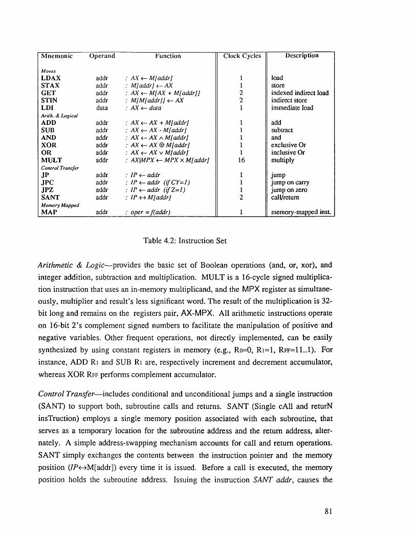
M nem onic Operand Function Clock Cycles Description
M ovesLDAX addr AX < - M[addr] 1 loadSTAX addr M[addr] < - AX 1 storeGET addr AX <r~ M[AX + M[addr]] 2 indexed indirect loadSTIN addr M {M l addr]] <- AX 2 indirect storeLDI data AX < r- dala 1 immediate loadArith. & LogicalADD addr AX <— AX + M{ addr] 1 addSUB addr AX <— AX - M l addr] 1 subtractAND addr AX < r- AX a M l addr] 1 andXOR addr AX <— AX ® M[addr] 1 exclusive OrOR addr AX < r- AX v M l addr] 1 inclusive OrM U L T addr AX\MPX <- MPX x M[addr] 1 6 multiplyControl Transfer
JP addr IP <— addr 1 jumpJPC addr IP addr ( i fC Y -1 ) 1 jump on carryJPZ addr IP <— addr ( i fZ = l ) 1 jump on zeroSAN T addr IP <-> M l addr] 2 call/returnMemory MappedM A P addr oper =f(addr) 1 memory-mapped insL
Table 4.2: Instruction Set
Arithmetic & Logic—provides the basic set of Boolean operations (and, or, xor), and integer addition, subtraction and multiplication. MULT is a 16-cycle signed multiplication instruction that uses an in-memory multiplicand, and the MPX register as simultaneously, multiplier and result’s less significant word. The result of the multiplication is 32- bit long and remains on the registers pair, AX-MPX. All arithmetic instructions operate on 16-bit 2 ’s complement signed numbers to facilitate the manipulation of positive and negative variables. Other frequent operations, not directly implemented, can be easily synthesized by using constant registers in memory (e.g., Ro=0, R i=l, Rff=11..1). For instance, ADD Ri and SUB Ri are, respectively increment and decrement accumulator, whereas XOR R ff performs complement accumulator.
Control Transfer—includes conditional and unconditional jumps and a single instruction (SANT) to support both, subroutine calls and returns. SANT (Single cAll and returN insTruction) employs a single memory position associated with each subroutine, that serves as a temporary location for the subroutine address and the return address, alternately. A simple address-swapping mechanism accounts for call and return operations. SANT simply exchanges the contents between the instruction pointer and the memory position (/P<-^M[addr]) every time it is issued. Before a call is executed, the memory position holds the subroutine address. Issuing the instruction SANT addr, causes the
81

contents of IP to be swapped with the contents of memory position addr. Now IP contains the subroutine address, while the memory position saves the return address. Thisoperation executes a subroutine call. Issuing the instruction SANT addr again, originates the same swapping operation, performing a subroutine return. To guarantee that after returning, the memory position will contain a correct subroutine address, a jump to the actual subroutine address must follow the SANT instruction which is used to return. The code fragment below illustrates the mechanism.
SANT rout_A ; call subroutine A
rout A: dw A addr ; contains the actual subroutine address
A addr:SANTJP
rout_A A addr
beginning of subroutine A subroutine returnafter returning, position rout_A points to a correct entry address
SANT executes in two cycles, using a memory read-modify-write operation. Since each subroutine has its own temporary saving position, nested calls are fully supported, but recursion is not. Compared with conventional stack-based systems, the mechanism used by SANT presents two main disadvantages: firstly, it consumes a fixed number of memory positions (one used as temporary saving position and one corresponding to the extra jump); and secondly, it does not support recursive subroutines (these are detected by the compiler). The main advantages of this approach are: to avoid a hardwired control for a stack, and to merge call and return operations into one single opcode.
Memory-Mapped—comprises a set of single-cycle instructions whose functions are associated with specific memory addresses. Memory-mapped instructions expand the
processor’s functionality at a little cost in silicon area (they use a decoder already required for the memory-mapped registers). The use of these specialised instructions reduces CPU overhead and increases code density. Memory-mapped instructions have the form of MAP addr, where the first 4 MSB of addr specifies the actual function. Fourteen memory-mapped instructions have been implemented (Table 4.3).
Most of these instructions are dedicated to control operations, associated with the communication unit, interrupt controller, timer, and ROM, and provide low CPU latency and
shorter service routines. Two of these memory-mapped instructions execute arithmetic
82
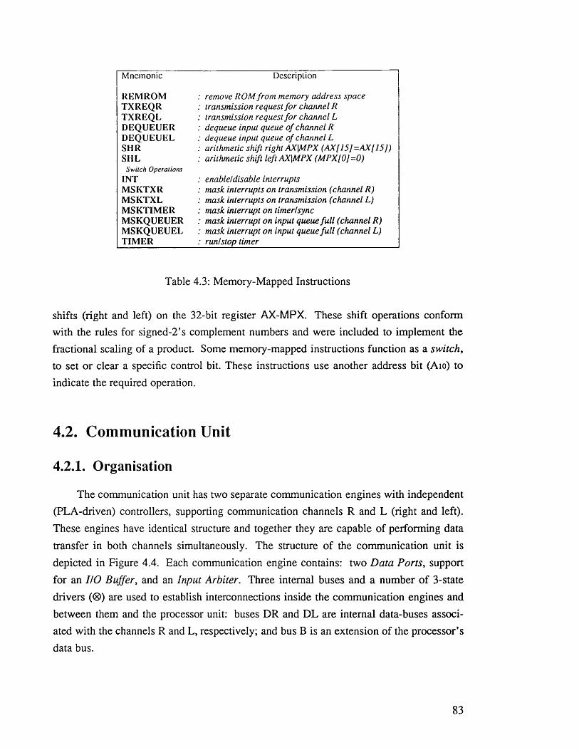
M nem onic D cscriplion
REM ROM : remove ROM from memory address spaceTXREQ R : transmission request for channel RTXREQ L : transmission request for channel LDEQUEUER : dequeue input queue of channel RDEQUEUEL : dequeue input queue of channel LSHR : arithmetic shift right AX\MPX (AX[15]=AX[15J)SHL : arithmetic shift left AX\MPX (MPX 10] =0)
Switch OperationsINT : enable/disable interruptsM SKTXR : mask interrupts on transmission (channel R)M SK TXL : mask interrupts on transmission (channel L)M SK TIM ER : mask interrupt on timer/syncM SK Q UEUER : mask interrupt on input queue full (channel R)M SK Q UEUEL : mask interrupt on input queue full (channel L)TIM ER : run/stop timer
Table 4.3: Memory-Mapped Instructions
shifts (right and left) on the 32-bit register AX-MPX. These shift operations conform with the rules for signed-2’s complement numbers and were included to implement the fractional scaling of a product. Some memory-mapped instructions function as a switch, to set or clear a specific control bit. These instructions use another address bit (Aio) to indicate the required operation.
4.2. Communication Unit
4.2.1. Organisation
The communication unit has two separate communication engines with independent (PLA-driven) controllers, supporting communication channels R and L (right and left). These engines have identical structure and together they are capable of performing data
transfer in both channels simultaneously. The structure of the communication unit is depicted in Figure 4.4. Each communication engine contains: two Data Ports, support for an HO Buffer, and an Input Arbiter. Three internal buses and a number of 3-state
drivers (®) are used to establish interconnections inside the communication engines and between them and the processor unit: buses DR and DL are internal data-buses associated with the channels R and L, respectively; and bus B is an extension of the processor’s data bus.
83
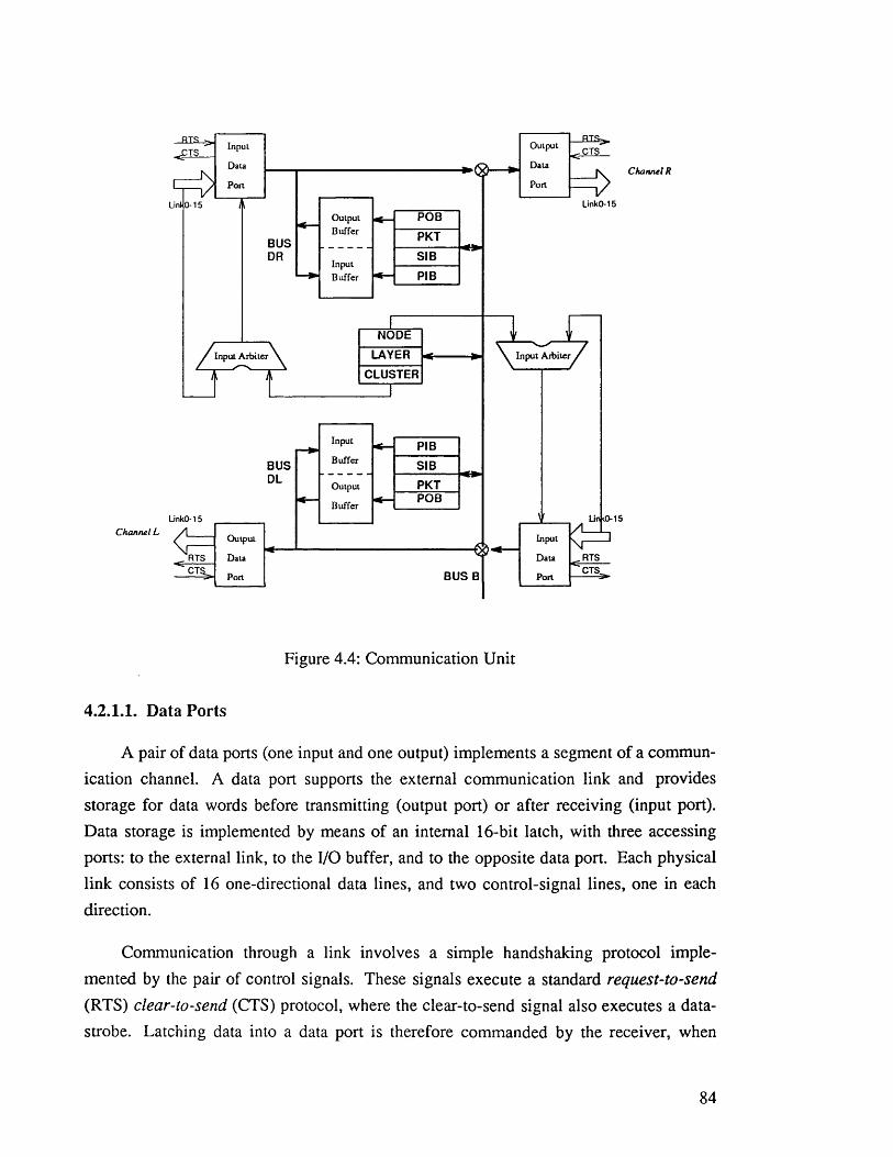
R IS > .CTS<
Channel R
LinkO-15Linl 0-15
BUSDR
Input A rbiterInput A rbiter
BUSDL
LinkO-15
RTSRTSCTS.BUS B
Data
Port
Output
Data
Input
Port
Port
Input
Data
O utput
Data
Port
CLUSTER
LAYER
NODE
SIB
PIB
PKTPOB
SIB
PKT
POB
PIB
O utput
Buffer
Input
Buffer
O utputBuffer
InputBuffer
Figure 4.4: Communication Unit
4.2.I.I. Data Ports
A pair of data ports (one input and one output) implements a segment of a communication channel. A data port supports the external communication link and provides
storage for data words before transmitting (output port) or after receiving (input port). Data storage is implemented by means of an internal 16-bit latch, with three accessing ports: to the external link, to the I/O buffer, and to the opposite data port. Each physical link consists of 16 one-directional data lines, and two control-signal lines, one in each direction.
Communication through a link involves a simple handshaking protocol implemented by the pair of control signals. These signals execute a standard request-to-send
(RTS) clear-to-send (CTS) protocol, where the clear-to-send signal also executes a data- strobe. Latching data into a data port is therefore commanded by the receiver, when
84

room to buffer another word is available.
The data transfer mechanism of data ports works according to the mode of operation in progress: receive, receive & forward, forward only, or transmit. Low-latency communication with neighbouring processors is achieved by overlapping several data transfers in each cycle time: the input data port can receive a new data word from a neighbour processor and transfer the previous word, simultaneously, to the I/O buffer and
to the output data port, while the output data port can pass an earlier word to the next neighbour processor. When the input data port tries to write to a full queue (FIFO buffer), communication in that link is blocked until some data is removed from the queue (namely, the result of the processor consuming a previously received packet).
4.2.I.2. I/O Buffer
The I/O buffer uses a separate block of RAM (which is also a data memory RAM), and a set of four memory-mapped registers that control its operation. Each I/O buffer is associated with a pair of data ports (input and output ports). Buffers have programmable size; the area not used for buffer can still be used as data memory by the processor. The processor unit and the communication unit can access the buffer to read or write a data word at any cycle, without causing conflict.
The I/O buffer works as a circular FIFO buffer (or queue) for input, and as a simple memory buffer for output. A queue allows the receiver and the sender to run at their own speed, relaxing the coupling of execution in communicating processors. A large queue relieves the input bottleneck thus increasing communication efficiency of the array. A simple output buffer provides the necessary support to send packets in burst or in single mode. Below, we describe the organisation of the I/O buffer separately, as an input queue and as an output buffer.
As an input queue, the allocated buffer area inside the RAM block must correspond to an integer number of packets (A/). Three communication-unit registers control the
queue operation: PIB points to current position to store the next word; SIB always points to the beginning of the queue and is used to circulate the queue, and PKT is a counter that holds the number of packets, corresponding to words positions still available
in the queue. These registers are initialised according to the required depth for the queue and the size of data packets. The processor implements an independent set of pointers in
memory to access the queue. During operation, register PKT can be accessed by both,
85

the processor and the communication units. PKT is incremented by the processor each time it consumes a packet, and it is decremented by the communication unit when an incoming packet is added. The condition of full queue is indicated by PKT=0, which causes a processor interrupt to be generated, while PKT=N denotes an empty queue. PKT works as a counting semaphore for increment and decrement operations. To guarantee coherent operation of the queue, concurrent access to PKT operations is resolved by means of a simple arbitration circuit and a memory-mapped instruction (DEQUEUE). DEQUEUE increments PKT, freeing buffer area equivalent to one packet.
As an output buffer, a single register (POB) is used to point to the beginning (and
current position) of the buffer area. The processor loads the corresponding buffer area with packets to transmit and sets the POB register. After transmitting each packet, the communication unit generates an interrupt. The processor then updates POB in order to point to the next packet to be transmitted.
4.2.I.3. Input Arbiter
The Input Arbiter consists of a number of binary comparators with access to the input data link and to the processor’s network-address registers: NODE, LAYER, and CLUSTER. The function of the Input Arbiter is to determine if an incoming packet is addressed to that node or it is en route to another processor. In other words, the Input Arbiter identifies the packet mode {node, layer, cluster or broadcast) and takes the necessary action. To accomplish this task the Input Arbiter checks the contents of the Network Identifier field of incoming packets against its internal network addresses (held in the registers), and against the global broadcast address (built-in). Address checking is performed in half a cycle (before the second word of a packet has been clocked into the input data port), allowing the packet to be clocked out to its destination(s) without interruption. The Input Arbiter has the ability to feed the packet on for delivery to the next processor node, feed it down to the I/O Buffer, or both, in case of casting mode packets. If a packet’s network address matches more than one internal address, the Input Arbiter follows an order of priority to name that particular packet (Table 4.4).
86

Priority Network Address1 node2 broadcast3 layer4 cluster
Table 4.4: Network Address Checking Priority
The objective of this scheme is to provide flexibility, by allowing some of the addressing modes to be turned off. When two internal network addresses are identical, the one with lower priority is ignored. For instance, if the contents of registers NODE and CLUSTER are made identical, the processor node will receive but, will not forward, packets that contain this network address.
4.3. Memory Unit
4.3.1. Organisation
The memory unit has an extremely simple organisation which consists of five parts: an instruction and data static RAM block; two identical static RAM blocks used as I/O buffers for the communication unit and as data memory for the processor unit; a small block of ROM for a (bootstrapping) resident code; and a Decoding & Control Unit. Words in all memory blocks are 16 bits wide. To access these memory blocks, a combination of buses and 3-state transceivers (<8>) are used. The block diagram of the memory unit is shown in Figure 4.5.
4.3.1.L Mapping of Address Space
The address operand (12-bit) specifies a 4K memory address space in direct mode. The memory blocks share this address space together with memory-mapped registers and
memory-mapped operations. Figure 4.6 shows the address distribution.
In order to keep most of physical addresses available to implement instruction and
data memory, two artifices have been introduced. Firstly, the ROM addresses are superimposed on the beginning of the instruction and data RAM addresses. During the
bootstrapping phase, read operations to those addresses actually access ROM, while write
87

address data
AL AR A B DR DL
0 2Channel R I/O Buffer
01
Data RAMI___0 2
Channel L I/O Buffer .
01 01
Data RAM
Read Select
Write
Read
Write Read-write-modify
Bootstrapping ROM
Instruction & Data
RAM
Decoding & Control
Unit
Figure 4.5: Organisation of Memory Unit
operations still access the RAM. (However, read-modify-write operations access the
RAM memory all the time, to allow the execution of SANT instructions and to give access to the interrupt vector table). This way, all RAM locations can be used for downloading the code that configures the processor node. At the end of the bootstrapping
phase (indicated by the instruction REMROM), the ROM is simply removed from the address space and all subsequent accesses to that area select the RAM for read and write
operations. The second artifice consists of assigning the same set of 14 addresses for the memory-mapped instructions and memory-mapped registers. These actually form the only set of addresses not available for implementing memory.

0Bootstrapping ROM
Inst. & Data Memory
I/O Buffer Channel R
I/O Buffer Channel L
Memory-mapped4096
Figure 4.6: Distribution of the address space
4.3.I.2. Decoding & Control Unit
The Decoding and Control unit contains logic which provides chip-select generation for the memory blocks, memory-mapped registers, and memory-mapped instructions. In addition, it generates a number of signals to control read, write and read-modify-write operations, and to remove the bootstrapping ROM. Block-select and control signals can be active twice in each clock cycle, to allow double memory access per cycle. The Decoding & Control unit achieves efficient management of memory blocks by employing a mechanism that allows concurrent access to these blocks without stealing cycles from the processor and communication units. Access to memory blocks observes the following rules:
Instruction and Data memory: the processor unit can access it for read or write operations in both phases (O; and d>2 ) of a clock cycle; the only exception is during bootstrapping, when the access is limited. Read-modify-write operations access exclusively this block of memory and occur when an interrupt is acknowledged, or when the instruction SANT is executed.
HO Buffer and Data Memories: the processor unit can read and write any position of these blocks of RAM in the second phase (d>2 ) of every clock cycle. During the first phase (O;), the communication unit has exclusive access to execute queue and buffer operations. As data references never occur during (refer to section 4.4.1), these blocks may be used as both an extension of the processor’s data memory and as an I/O buffer.
89

Bootstrapping ROM: this block becomes active after reset and it is removed by reseting the ROM flag (REMROM instruction). It is accessed only by the processor, during
bootstrapping phase.
4.4. Operation
4.4.1. Processor Unit
This section describes the operation of the processor unit which includes: reset and bootstrapping procedures, instruction pipeline, and interrupt processing. (Details about the clock system and processor speed can be found in Chapters 6 and 7).
Reset and Bootstrapping
Processor initialisation is accomplished by driving the RESET input pin high. RESET sets some registers to predefined values, disables interrupts, and enables the bootstrapping ROM.
The bootstrap code performs a initial setup of the interrupt controller and communication unit, and waits for packets to arrive. The initial setup specifies all internal network addresses equal to zero (Node=Layer=Cluster= all 0 ’s) and packet size equals 32 words. The first packet that arrives contains configuration information, such as the processor’s actual network addresses and loading details (load counting and load starting address). Subsequent packets carry the processor’s configuration data that are loaded into specific segments of the RAM memory. At the end of the loading phase, the program issues the REMROM instruction, which disables the ROM and resets the instruction pointer, commanding the processor to execute the code recently loaded. An external synchronisation signal (SYNC) can be optionally used in timed applications. SYNC generates an interrupt to all processors, allowing them to start in step-synchronism.
Instruction Execution
Instructions differ in the number of memory accesses performed during execution:
• no access: 4 instructions plus 14 memory-mapped instructions.
• one access: 7 instructions.
90

• two accesses: 3 instructions.
• sixteen accesses: 1 instruction (MULT).
Memory access can occur twice per cycle. As a result, almost 86% of all instructions execute in one single cycle. To achieve this rate, time-demanding operations such as ALU operations and IP updating, were allowed to take a full clock cycle, and to execute concurrently with other processing operations. When defining pipeline stages, operations were carefully grouped into each phase and additional cycles introduced, in order to obtain minimum clock phases. In such cases, a semi-cycle (NIL) is wasted in order to even up the number of instructions’ cycles.
The diagram in Figure 4.7 illustrates the stages in the execution pipeline.
phase 1
phase 2
icycle 1 i cycle 2
ii
FD EX
PC
WB
FD EX
FD EX
FD EX
FD EX
FD EX NIL WB
FD EX1 EX2 WB
Clock
FD: Fetch & Decode EX: Execution WB: Write Back PC: Program Counter Update
- single-memory-access
instructions and immediates.
-ALU operations.
- next intruction.
- indirect load and store.
- SANT instruction.
Figure 4.7: Instruction Stages

An instruction is fetched and decoded in the FD stage. In the execution stage (EX), the operand (if present) is fetched and the instruction begins to execute. The result of the operation is written back to a memory position or to a register in the writeback stage (WB). Simple instructions combine the EX stage with WB stage to finish in one cycle. PC corresponds to instruction pointer updating stage. A PLA controls the execution of the pipelining stages of the Neural-RISC processor. Machine states change at every
phase (twice per cycle).
Fetch & Decode stage: This stage is identical for all instructions, regardless the operand type: albeit a memory address or an immediate constant. Instruction fetching
and decoding takes only half of a clock cycle.
Execution and Write Back stages: Instructions that reference memory once or make no memory access (immediates) use one EX half cycle (Figure 4.7). For jumps, the condition is evaluated, and if the jump is taken (condition true), the control terminates the instruction pointer incrementing, and writes IP using the EX stage. Instructions that perform arithmetic and logic operations in the ALU (except MULT) enter the EX stage to read data from memory, compute the necessary function, and latch the results. This stage extends for one complete cycle. Because the processor contains the necessary bypass paths, it can write the result back to the accumulator and to the condition code register, at the same time as the next instruction is fetched and decoded. Indirect load and store instructions use the EX stage to get the operand address, and a separate WB stage, to read or write the memory. The instruction SANT performs a read-write-modify operation retaining the processor’s paths for two EX stages and a WB stage (Figure 4.7).
Interrupt Processing
All interrupts are sampled at the end of each instruction. Therefore, an interrupt request can take as short as one cycle, or as long as 16 cycles (multiply) to be serviced. The interrupt controller responds identically to all interrupts. If an interrupt request is pending, the processor acknowledges the request and executes a procedure similar to that performed by the instruction SANT (section 4.1.2). Execution transfer takes only one
cycle. When an interrupt is acknowledged, the interrupt controller resets the interrupt flag IF, and further interrupts are disabled. The interrupt flag will remain zero unless specifically set in the interrupt routine. To re-enable interrupts the program must issue the memory-mapped instruction INT, that sets the interrupt flag. This operation is delayed for two cycles, so that the following instruction begins to execute before another
92

interrupt is serviced. This mechanism permits an interrupt routine to re-enable interrupts only after the last instruction (usually a "return"). To allow nested interruptions, the interrupt routine must first reset its own mask bit to guarantee that another interrupt request from the same source do not generate an interrupt.
4.4.2. Communication Unit
This section describes interprocessor communication, and shows how it is supported
by the Neural-RISC processing and communication facilities.
Neural-RISC processors operate independently and communicate with other processors by sending and receiving message packets. Communication occurs asynchronously with the processors’ left and right neighbours, through unidirectional channels. Packets are sent directly from the sender’s data structures to the receiver’s data structures, without any memory buffering at intermediate processor nodes. Processors simply forward the packets over the communication channel, down to the destination nodes. Since a channel is built link by link, packets can take longer to be forwarded if some links are temporarily unavailable. A link between two processors can be temporarily unavailable if the following processor in a channel is transmitting a message, or if the input queue of a recipient node is full. (An intermediate node with full queue can still forward packets). The throughput of a channel is maximised by defining input queues sufficient large to match the processing time of the algorithms running on each node. The Neural-RISC processor provides the user with programmable-size input queue and output buffer, and two basic modes for programs to control the I/O of packets: a polled mode and an interrupt-based mode. Both modes are used to control input, while output is always based on interruption.
For input, the packet counter (PKT) supports both polled and interrupt-base modes. Polling the communication channel is accomplished by reading the associated packet counter. The contents of PKT indicates to the program if a packet has arrived. Alternatively, individual node programs can set the processor to generate an interrupt when a specific number (N) of packets have arrived. N actually corresponds to the depth of the queue for the specified packet size, and the interrupt indicates that the queue is full.
For output, an interrupt is generated by the communication unit after transmitting each packet. To transmit a message, the sender takes three steps: firstly, it determines the communication channel(s) to send that message (for instance, the one that provides
93

the shortest path to reach the destination node); secondly, the sender prepares a number of packets, stores them on the appropriate output buffer, and sets the corresponding pointer (POB) to the first packet; finally, it sets a transmission request (memory-mapped instruction TXREQ) and continue with its processing regardless the availability of that channel. When the channel is available, communication unit spools (word-by-word) the data out of memory, and transmits the packet over the channel. The end-of-transmission
interrupt allows the output process to point to the next packet in the buffer (if any), or terminate transmission.
94

Chapter 5
Architecture Simulation
This chapter deals with the simulation of the system and node architectures. Itdescribes the simulation framework, presents the evaluation procedures, andsummarises the results obtained.
The architecture simulation studies involved the implementation of three software simulators and investigated several alternatives for the Neural-RISC system and node architectures. These studies provided an effective method of assessing and improving the architecture design.
The first simulator, developed in the early stage of the architecture specification, investigated the minimal implementation of a RISC architecture. We focused our attention on the processor instruction set and evaluated architectures containing very few instructions, i.e., one, two, four and eight instructions23,71,104. These alternatives were soon discarded because of the large memory required for programming.
In a second phase, we considered a 16-instruction processor and simulated an architecture composed of a single processor array. Later, this design evolved into a multi-ring architecture which was the origin of the simulator described in this chapter.
5.1. Simulation Framework
This section describes the main features of the simulation framework which includes the architecture simulator and a simulation environment for programming neural network models. The simulation environment provided support for another work20, combining research in two distinct areas— neurocomputer architectures and neural network programming systems. The heart of the simulation environment is the software simulator that performs the neurocomputer.
95
5.1.1. Software Simulator
Implementing the multi-processor parallel architecture in software required writing
a program that simulates the system components (i.e., processors and rings) as individual instances. These instances were then called together in sufficient number to build systems of diverse sizes and configurations. To allow the investigation of various design alternatives, the simulator realises the system components through configurable units. A user interface was also required so that it was possible to actually program the simulator, debug application programs and assess the architecture performance. To this end, a set of tools was designed and incorporated to the simulator through a user-interface module. Much of this code is required for gathering statistics, providing debugging facilities and managing the occurrence of timed events in the parallel network. The simulator itself was written in the programming language C and consists of about 5000 lines of code. (The ELLA language1 and software simulator were first considered as simulation vehicles. However, problems with earlier versions of this system have made us to opt for a conventional programming language). The simulator is distributed over five modules:
Main simulates an instance of the complete system: the host and the system andnode architectures.
Config a module containing a set of configuration parameters such as:number_of_rings, ring_size, master_clock, memory_size, etc.
Userint provides the user with the ability to modify, examine and control execution. The user interface includes: 15 menu-driven commands; 13 different break points based on marked events; and 4 automatic log-files to record the system statistical data.
lnst_Exec the instruction execution module contains the code for executing thecurrent instruction set.
lnst_Set the instruction set descriptor defines the instructions’ mnemonics,opcodes, time delays, and pointers to the execution routines.
The simulator configures the system and node architectures by defining their components in a global data structure. In C, this was implemented by describing the many
features of each component in structures and building the system hierarchically.
96
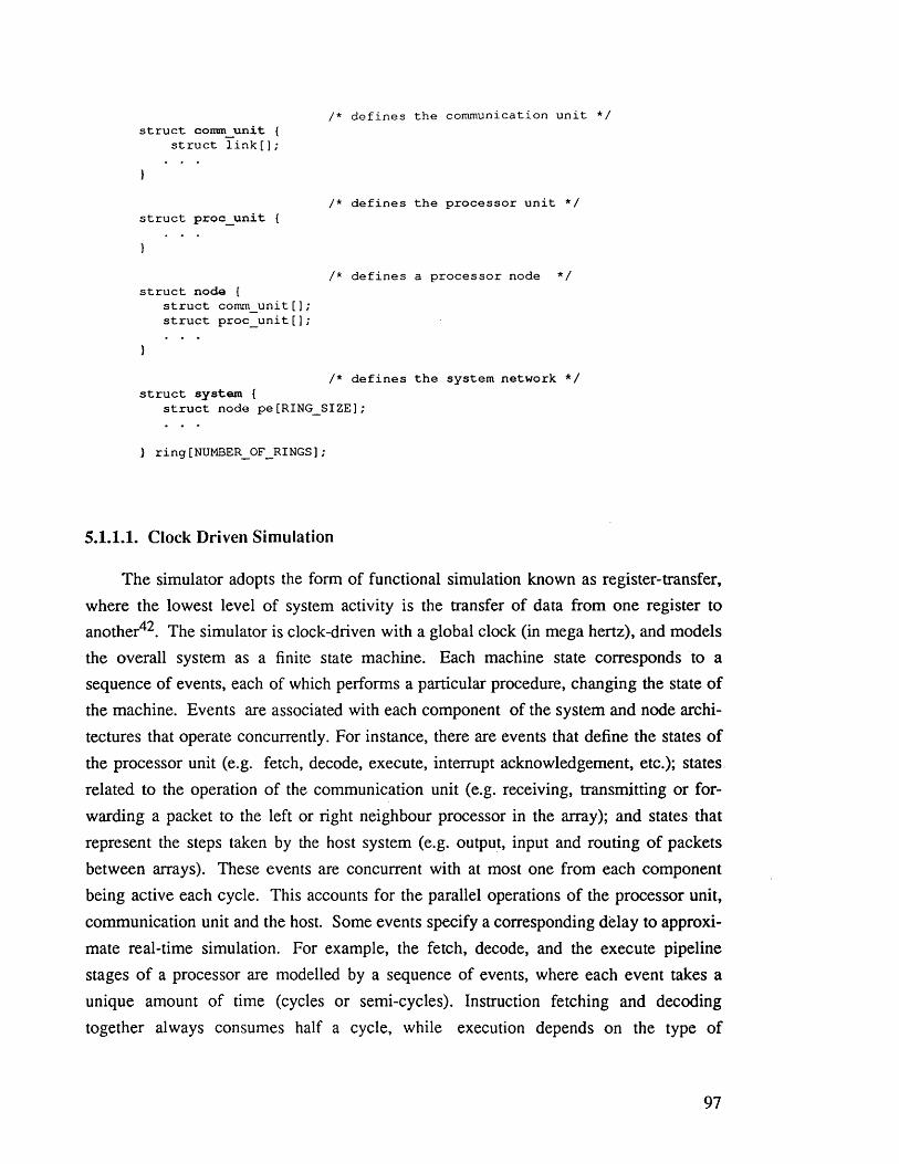
/* defines the communication unit */struct commjanit {
struct link[];
}
/* defines the processor unit */struct proc_unit {
}
/* defines a processor node */struct node {
struct comm_unit[]; struct proc_unit[];
}
/* defines the system network */struct system {
struct node pe[RING_SIZE];
} ring[NUMBER_OF_RINGS];
5.1.L1. Clock Driven Simulation
The simulator adopts the form of functional simulation known as register-transfer, where the lowest level of system activity is the transfer of data from one register to another42. The simulator is clock-driven with a global clock (in mega hertz), and models the overall system as a finite state machine. Each machine state corresponds to a sequence of events, each of which performs a particular procedure, changing the state of
the machine. Events are associated with each component of the system and node architectures that operate concurrently. For instance, there are events that define the states of the processor unit (e.g. fetch, decode, execute, interrupt acknowledgement, etc.); states related to the operation of the communication unit (e.g. receiving, transmitting or forwarding a packet to the left or right neighbour processor in the array); and states that represent the steps taken by the host system (e.g. output, input and routing of packets between arrays). These events are concurrent with at most one from each component being active each cycle. This accounts for the parallel operations of the processor unit, communication unit and the host. Some events specify a corresponding delay to approximate real-time simulation. For example, the fetch, decode, and the execute pipeline stages of a processor are modelled by a sequence of events, where each event takes a unique amount of time (cycles or semi-cycles). Instruction fetching and decoding together always consumes half a cycle, while execution depends on the type of
97

instruction (single-cycle, double-cycle, etc.).
The simulator scans the whole system at each cycle, simulating all events that are due at the current global time. Typically, these events perform operations such as a register transfer, ALU operations, and word transmission, changing the components’ status. After all events have been simulated, the time is advanced by one unit and the process is repeated. To interrupt this process, the user sets break points to detect the occurrence of specific events. The global clock represents the expected machine clock and it is programmed in units of mega hertz. However, the real clock speed will actually depend on the technology of chip integration.
The following section briefly describes the simulated architecture which served as the basis for the final design.
5 .I.I.2 . Simulated Architecture Overview
The simulated architecture is a previous conception of the Neural-RISC architecture, which corresponds to a close version of the actual architecture implemented in silicon. It contains the basic features of the current system and node architectures and served as a prototype to produce the current version (problems found in the simulated architecture were fixed and new features incorporated to the VLSI design). The distinguishing features of the simulated architecture relative to the actual Neural-RISC system and node architectures are listed below.
System Architecture
System Configuration. This is a simplified version of the system architecture which consists of a number of processors’ rings and the host. There are no Link Interface modules. Instead, rings end up in the host computer, which incorporates part of the routing algorithm for supporting inter-ring communication.
Message-Routing System. Packets are fixed length and consist of three 16-bit words containing: the destination node address, an input port number and a data value. The system supports only two network addressing modes: node and global broadcast.
Node Architecture
Register Set. The processor includes a smaller set of registers consisting of: the accumulator AX; the instruction pointer IP; an auxiliary instruction pointer IPX to save IP during
98

interruption; a memory address register MAR and a memory data register MDR used in memory accesses; and a processor status word PSW.
Instruction Set. The instruction set contains 16 instructions which used a format similar to one adopted in the current version, i.e., a 4-bit opcode and a 12-bit operand. Some operations such as multiplication and the subroutine call, not directly supported in this version, are implemented by sequences of instructions. The instruction indirect jump
(jpin) supports return from subroutines. Table 5.1 lists the basic instruction set imple-m e n te d .
Mnemonic Operand Function Clock Cycles DescriptionMovesldax addr AX < r- M[addr] 1 loadstax addr M[addr] <— AX 1 storeIdin addr AX < r- M[M[addr]J 2 indirect loadstin addr M[M[addrJ] <— AX 2 indirect storeArilh. & Logicaladd addr AX <- AX + M[addr] 1 addsub addr AX < - A X - M[ addr] 1 subtractand addr AX <— AX a M[addr] 1 andxor addr AX <— AX © M [ addr] 1 exclusive Oror addr AX < - AX v M[addr] 1 inclusive Orrr - AX[n-l] < r- AX[n] 1 rotate rightrrc - rr, AX[15] <— CY 1 rotate right through carryControl Transfer
jP addr IP <— addr 1 jumpjpc addr IP < r-addr (i f C Y - 1 ) 1 jump on carryJPZ addr IP <- addr (if 2=1) 1 jump on zerojP 'n addr IP < r- M[M[addr]] 2 indirect jumpreti - IP <— IPX, enable int. 1 return from interrupt
Table 5.1: Simulated Instruction Set
Communication Unit. The communication unit provides support for four unidirectional links, each link consisting of 16 data lines and three handshaking signals (a request to send, a clear to send and a strobe signal). Associated with each link (one input and one output), three (16-bit) latches provide storage for a complete packet.
HO Buffer. The I/O buffer actually realises the interface between the processor unit and communication unit. It is implemented by two sets of dual-ported registers, capable to
store a single packet in each direction (input and output). The access and current condition of this buffer is controlled by a buffer status word (BSW), accessible by both, the processor and communication units.
99

5.1.2. Simulation Environment for Neural Network M odels
In addition to aiding in the design choices for the neurocomputer architecture, the simulator was also used to evaluate a neural network programming system (NPS), designed as part of another project26. This programming system incorporates a specialised language called NIL (Neural Network Implementation Language), designed to map a spectrum of neural models onto parallel architectures25. NIL provides mechanisms for specifying the functions of the nodes and the interconnection topology of the neural network. The computational model of a function that represents a node is based on the generalised model of a biological neuron, i.e., an output is produced only when a set of input conditions is satisfied. As an intermediate language for neural networks, NIL expresses parallelism implicitly, that is, it reflects the parallel nature of algorithms in its constructs and expressions.
To test the neurocomputer with practical applications and to assess the capabilities of the language in supporting neural algorithms, a simulation environment was designed and implemented in collaboration with Siri Bavan. The structure of the simulation environment is shown in Figure 5.1. It consists of:
1) NIL Compiler—to generate the assembly code to be executed on each processor of the simulated architecture.
2) Assembler—to convert the assembly code into executable object code.
3) Algorithms Library— which consists of a set of standard models such as Hopfield, Backpropagation, and Boltzmann machine, coded in NIL.
4) Mapper—to map and load neuron nodes into the simulated processors.
5) Architecture Simulator—that simulate the neurocomputer in size and configuration as specified by neural algorithms.
6) Boot—the assembly code that implements the processors’ bootstrapping.
7) Service— which implements a set of I/O and interrupt service routines for assisting neural network applications.
When using the simulation environment, neural network models coded in NIL are taken from the library and compiled, producing the assembly code correspondent to the
network of processors. The assembler then checks the instructions syntax and generates the equivalent object code. The mapper simply reads the object-code files and loads the
100

AlgorithmsLibrary
Service
Boot
Input
V
NPSCommand Interpreter
Mapper
/ / \ N
■ctod-Cti
Ckxj-O!
OOO-Oi
Architecture Simulator
NIL Compiler
Neural-RISC
Assembly
Program
Assembler
Neural-RISC Object Code
Figure 5.1: Simulation Environment
simulator in sequence. During trials, the simulator was used to run different models, assessing both, the language capabilities and the parallel architecture. Examples of neural models coded in NIL can be found in Appendix 1 and in2 .
Having briefly described the simulation framework, the following subsections present the simulation results and the consequent changes to the architecture.
5.2. Simulation Results
This section presents the most important contributions from the simulation studies
to the design of the Neural-RISC system and node architectures. The analysis of the
101
statistical data resulted in a number of changes to the original architecture. In summarising these changes, emphasis is placed in two areas. Firstly, the instruction set usage and its implications to the processor architecture, and secondly the communication overheads
in the point-to-point structure.
5.2.1. Instruction Set Usage
Following the RISC philosophy, a minimal set of instructions (16) was initially chosen for the processor. The choice of the instruction set greatly affects the usability, implementation, and performance of the computer system. To examine these issues, we have analysed the code generated by the NIL compiler to determine how well it used the instruction set. The probability of occurrence of each instruction allowed us to improve code density and to achieve an optimal dimensioning of the hardware associated with the most used instructions.
We examined a moderate number of benchmarks in detail on the Neural-RISC simulator. These benchmark applications are neural network algorithms, written in NIL and compiled to assembly code for the simulator. Figure 5.2 displays the distribution of instructions into five classes: moves (or data transfer), control transfer, arithmetic, logic, and rotates. This distribution is in accordance with several other studies on instruction- set statistics *9,20,53
However, the detailed breakdown of instructions presented some discrepancies that helped us to draw important conclusions and to examine some innovations on the processor architecture (Figure 5.3). The graph shows that some instructions are seldom used by the compiler, while others exhibit a considerable high frequency. The "rotate" instruction (rr), for instance, does not occur at all in the compiled code. This is largely because there is a rotate through carry (rrc) instruction which performs almost identical operation.
The high frequency of store, add, and indirect-load instructions was clearly indicated by the nonexistence of immediate and indexed addressing-mode instructions. This
forced the compiler to repeatedly use the sequence of instructions in Figure 5.4a to read data structures.
Analogously, the lack of procedure call instruction, contributed for the high rate of store, load, add and jumps. The sequence in Figure 5.4b is widely found in the compiled code.
102
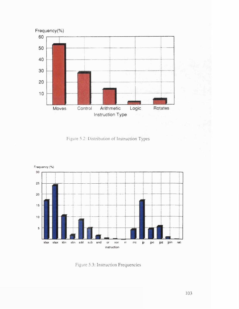
Frequency(%)
Moves Control Arithmetic Logic RotatesInstruction Type
Figure 5.2: Distribution of Instruction Types
25
2 0
15
10
5
Idax s tax tdin stin add sub a n d or xor rr rrc jp jpc jpz jpin reti
Instruction
Figure 5.3: Instruction Frequencies
Frequency (%)
103

In each of these examples, there is a waste of at least 3 instructions, since the target operations could be implemented by single instructions. We therefore decided to include an indexed-load instruction (GET) and the instruction SANT to support these operations. GET packs an ALU operation with memory references into a single machine instruction. SANT supports both nested procedure calls and returns by means of a special swapping mechanism (see section 4.1.2).
ldax INDEX add BASE stax POINTER ldin POINTER
(a)
ldax IP add THREE stax RET__ADDR jp ROUTINE
THREE: dw 0003
(b)
Figure 5.4: Fragments of the Compiled Code (a) Accessing Data Structures; (b) Implementing Procedure Call
The low frequency of the return-from-interrupt (rti), recommended us to perform
this operation with the instruction SANT. This change required passing the control of the interrupt enable flag to another instruction, since the processor could not distinguish between an ordinary return and a return from interrupt.
The high percentage of constants being implemented in memory (e.g. the constant THREE in the example above) proved crucial so the load immediate instruction was created, reducing by 50% the memory consumed with this operation. This idea is further
supported by the fact that the most frequently assigned values are small constants, between 1 and 16. Overall, roughly 40% of the small constants have value zero or one. The load immediate instruction (LDI), incorporated to the instruction set, includes a 12-
; specifies an element ; calculates address of an element ; saves the address ; reads an element
; implementing a CALL ; reads instruction pointer ; calculates return address ; saves return address ; jump to subroutine
; constant
104

bit immediate (the 4 MSB are extended to zero), sufficient to hold a memory address or a constant between 0 and 4095.
Among the various ALU operations, the most frequent are those relating to add and subtract. This fact is not surprising, since addition and multiplication are heavily used in neural network models for computing the expression: x,- = Z Wij.yj. The compiler implements multiplication through a 44-instruction subroutine which uses a standard (16- iteration) algorithm based on add/subtract operations. This code is very expensive in
terms of performance, and represents a potential bottleneck for the whole system, if we consider that each received packet originates a multiply operation. To alleviate this problem, the introduction of a two-bit multiply step instruction was investigated. Although this approach would allow us to keep in line with the RISC philosophy (i.e., single-cycle execution for most of the instructions), the total number of cycles required for the iteration control in software would virtually invalidate this effort. Therefore, a 16-cycle (signed) multiplication instruction (MULT) was incorporated to the instruction set.
A final observation on the code generated by the compiler showed us that a large number of load, store and logic instructions were being used to manipulate the processor status and control words (i.e., masking, setting or reseting specific bits). These codes were mainly employed in driving hardware devices such as the interrupt controller and communication unit. We evaluated the cost of having instructions for bit handling, i.e., test, set and reset operations on the contents of the accumulator. Our original analysis estimated that the bit selection hardware would have a significant penalty on the processor’s data-path. We saw that, the benefit of having an optimised device control and an improvement in code density, did not justify the introduction of these instructions from a performance viewpoint. Instead, we extended the instruction set to include (single-cycle) memory-mapped instructions that manipulate specific control bits. The expansion is custom-tailored for the context, since they utilise hardware already present in the data-path design.
5.2.2. Communication Issues
A limiting factor in the performance of parallel machines is the communication overhead. Communication efficiency is influenced by several factors, some of which are directly related to the communication system12. The topology of the interconnection network, the network size (i.e., the number of processors), the data exchange
105

communication protocol, the speed of data transmission, the support for buffering data, the traffic load, and the mapping of algorithms in the architecture are all significant in affecting the overall communication performance. In assessing the performance of parallel architectures for neural networks, some researchers have based their study on topological characteristics of the communication structure117, while others have explored the mapping of neural algorithms onto these systems46. In this section, we concern ourselves with architectural features of the communication structure, assessing their effectiveness and introducing changes where necessary. Since an accurate simulation would be very expensive and time consuming, we adopted a simple model, sufficient for describing the architecture details, and ran experiments exclusively to identify physical bottlenecks that determine potential communication overheads.
We have monitored the communication system by running a small set of neural network algorithms and a program to simulate the worse case for network traffic. The traffic intensity generated by this program is much higher than we expect to encounter in practical applications of neural networks, where mapping strategies try to minimise interprocessor traffic46,11 Consequently, the communication system should exhibit a superior overall performance in real applications.
To observe the communication flow, we employed several evaluative measures: average traffic load, average packet delay, percentage o f blocked links, and average HO processing delay.
Simulations have shown that the size of input buffers is the most critical factor in the efficiency of the communication system. In these simulations, the rate of unsuccessful attempts to receive incoming packets due to the lack of buffer space is unacceptably high. We see that for reasonable traffic intensities this rate can reach the mark of 93%, resulting in a comparable percentage of blocked links in the network at a given time. In the original design, buffer is provided for one packet only, meaning that an interprocessor link blocks with the arrival of a new packet if a previous one has not been consumed by the processor. Our simulations of neural algorithms indicated a processing average delay of 59 cycles per incoming packet, time sufficient to transmit or forward almost 10
packets in each link. The design of the communication unit was obviously not adequate. The problem was corrected by adopting variable-length input queues, implemented by FIFO buffers. This approach provides more flexibility by allowing queues to be tailored for specific applications, according to the expected traffic intensity. As a consequence of this modification, we released the restriction on the length of the packets, by supporting packets of programmable size, up to the size of the queue.
106

Although we considered the measured efficiencies somewhat encouraging, we noted that system performance could be improved even more by optimising a number of design features. We concentrated our attention on three issues: the packet switching procedure, the network addressing scheme, and the host. Originally, packet switching in the processor array was based on the store-and-forward principle. That is, incoming packets were completely stored in the processor’s buffer until they could be passed on to the next node. Storage was implemented by two set of 3-word buffers (one at the input, the other
at output), serving each communication channel. As a result, forwarded packets had to be clocked three times when crossing every intermediate processor. Since in the linear array there is no alternative routes for travelling packets, the store-and-forward procedure offers little advantage. To solve this problem, the packet buffers were eliminated and triple-ported single-word latches introduced, thus allowing packets to be clocked without interruption by the processor nodes, at a rate of one word per cycle.
We analysed in detail the traffic generated by several neural network models and concluded that most of the algorithms could efficiently use a kind of selective broadcast communication to reduce the large communication fan-out of specific nodes. When layered networks were mapped onto the multi-ring structure, a high volume of traffic was produced by nodes sending identical copies of a packet to nodes in the adjacent layer. When adopting global broadcast packets to spread the node output, the processing overhead increased in consequence of nodes having to read and discard unwanted packets. The network addressing scheme was clearly deficient. Therefore, we decided to support local broadcasting by introducing two group addresses: layer and cluster. To reach a specific group of nodes, processors prepare and send a single packet addressed to that particular group. The major effects of this innovation are the reduction of the global amount of traffic and a significant improvement in processing time.
Finally, we evaluated the absolute performance required from the host by examining the interarray traffic. A precise estimation for interarray traffic is difficult to obtain since it depends on neural network partitioning and mapping. However, using the various
records of traffic measurements produced by neural networks applications, we observed a relatively high rate of interarray traffic. In average, this rate stayed just over 50% of the total system traffic, with peak rates reaching 85%. To sustain the maximum traffic of all such applications, an specialised hardware component to support the ring ports should replace the host. This led us to the idea of using many clusters of rings, with a "multiring interconnect module" to handle the I/O between the processor arrays in each cluster.
107

Chapter 6
VLSI Implementation
This chapter describes the VLSI implementation of the Neural-RISC architecture. It starts by presenting the design approach, which considered the available VLSI design tools for the project. Next, it reports on the design of a modular cell library to implement specialised operative parts of the microprocessor. It then discusses the design strategies for the operative and control parts of the chip. Finally, it examines design considerations and results of the VLSI implementation.
6.1. VLSI Design Approach
The role of a good VLSI design is to reduce its complexity and to assure the designer a final product, consistent with its architectural and functional specifications. Before embarking on the physical implementation, one must consider a structured approach that trades the expected end results with the available tools and design methodologies for a particular chip132. Overall, the relevant attributes of a VLSI design can be summarised as follows:
• silicon area
• performance: speed and power
• implementation time
• testability , '
The first two attributes are particularly influenced by the silicon processing technology, while the last two attributes depend mostly on the design approach, design environment and on the designer’s expertise.
We investigated a number of design methodologies and estimated their impact on the design attributes. For silicon area, the primary objective was to pack multiple processors onto the silicon die, in order to evaluate future implementations with denser technologies. To meet this requirement, we enforced ourselves in the design of a highly optimised cell library, which could provide minimum area for the chip datapath. The performance constraints were also rigorously observed in the conception of these cells. The cell library was implemented in collaboration with Marley Vellasco and Carlo de
108

Oliveira, whose theses also involved VLSI d e s ig n ^ 8 ’ 127. (Section 6.2 describes the design of the cell library).
Given our limited experience with VLSI design and the timetable constraints of the
thesis, we sought to combine the available tools to take advantage of the automating procedures and leave a good deal of handwork out of the design. This approach offered the best prospects for dealing with a large design in a short time. By the time we started with the implementation, the VLSI design tools available were: the Berkeley tool set, in particular Magic108, and the CAD system Solo 2000 from European Silicon Structures2. Magic is an interactive editor for creating and modifying VLSI circuit layouts100. As a symbolic editor (it has knowledge of design rules), Magic provides better design resources than a simple layout editor. The disadvantage of using Magic is that it does not incorporate a complete design, verification, and test system, to attend all phases of an IC design. For instance, Magic offers limited support for automatic routing (it only deals with local routing) and does not work with schematics. On the other hand, SOLO provides a complete and integrated tool set, with a unified data structure, that includes: a schematic graphics editor, module generators for parameterised RAM, ROM and PLA, automatic placement and (global) routing facilities, and standard cells libraries for I.5|i and 2.0|i CMOS technologies5.
The option for SOLO seemed obvious, except that the version of SOLO we had available did not include the layout graphics editor. Consequently, there were two alternatives for implementing the processor’s datapath: firstly, to use Magic and integrate the layout into the SOLO environment; and secondly, to use the standard cells supplied by SOLO. From the viewpoint of simplicity and design automation, the alternative of using standard cells combined with the schematic editor, was certainly the most attractive one. However, silicon area would increase significantly.
To evaluate this alternative properly, we designed and implemented a toy microprocessor using standard cells all over the design. The microprocessor was proportionally
sized in order to provide a more precise idea of the effect standard cells would produce in our designs. The toy microprocessor was a 16-bit RISC containing: 2 instructions
(add&write and sub&write); a set of 8 (16-bit) registers; 512 words of RAM; and 64 words of ROM.
The results obtained from this chip were extremely discouraging. The device measured 7.9x5.2mm, with 42% of its area occupied by standard cells. Considering that the complexity of our actual designs were at least three times greater than that of the toy
109

microprocessor, the use of standard cells for the datapath was out of question. We therefore opted for the alternative which would result in the smallest size of die and could provide adequate basis for assessing performance and chip area of implementations with modern technologies.
Before starting the layout, we carried out an extensive analysis of the Magic’s technology file to determine how manageable would be converting it from the available 2 j i to
the 1.5ji technology. The analysis showed that the intended modification would demand a laborious work for reprogramming and testing Magic, which we considered outside the scope of the thesis. For this reason the chip was implemented in 2p. CMOS.
In order to achieve a highly integrated chip layout and to shorten the turnaround time in the layout design, we effectively applied the automated design system in all design levels. The flowchart diagram in Figure 6.1 describes the design environment used for the chip implementation. The chip layout consisted of a six-stage design process:
1) Cells Design: This involved the manual layout of bit cells and the automatic generation of the n-bit slices for each type of cell in the cell library. Cells were designed with Magic and their layouts exported to the SOLO environment by means of a software tool to convert formats (Calma to SDA). In the SOLO environment, three representations were created for each of these slices: a symbol for manipulating the slices in the design of the cell-blocks; a schematic, describing the slices’ logic behaviour for functional simulation; and an abstract representation with pin and cell boundary information for placement and routing.
2) Cell-Blocks Design: Cell-Blocks are functional units that combine the logic features of a number of slices. They implement registers, ALU and other functional elements, present in the datapath. Cell-Blocks were designed in three phases: firstly, they were laid out by abutment to check for DRC (design rules check) errors and for the need of blank-jumper cells between slices; secondly, schematics were produced for netlisting
and simulation purposes; finally, symbols were automatically created for later use in the chip integration.
3) Datapath Design: In this stage, cell-blocks were combined to implement datapath segments. Their design followed the same steps executed for the cell-blocks and also included the generation of a textual placement of the cells. This text records geometric characteristics related to cells abutment, rotation, and overlapping.
110

4) Macroblocks Design: Macroblocks are RAM, ROM and PL A modules created automatically through the SOLO module generators. The generation of RAM and ROM blocks and their representations is straightforward. For the PLAs, the process also involved truth-table generation (Eqntott) and Boolean minimisation (Espresso), before modules generation.
5) Random-logic Design: These are parts of the circuit that were designed with standard cells, using automated design programs for schematic editing and capturing.
6) Chip Integration: Producing the final chip layout involved many steps, all o f them
supported by the automated design tools. In the first step all components were integrated into a single chip schematic (Schematic Editor) for generating netlist and layout representations. Cells and blocks were placed using a semi-automated method for controlling terminals position and direction, in order to reduce the interconnection area. Routing was performed by SOLO’s advance routing program that supports automatic channel generation and control functions to specify routing objectives. In this process, layouts were checked for DRC errors and the design process repeated from the beginning. The final optimised and correct layout was then converted to Calma and sent to fabrication.
6.2. Datapath Cell Library
The cell library contains a total of 117 different cells, organised into three main classes: modular register building blocks, functional elements, and interface & switching
elements. The design of these cells follows a well-defined design philosophy for a balance between the minimum silicon area and high performance requirements.
6.2.1. Design Philosophy
As the complexity of VLSI chips increases, the need for a common, shared cell library becomes essential. Sharing cell library helps to prevent duplicate development efforts and promotes exchange of ideas for new cells architectures. In addition, it contributes to achieve rapid prototyping and allows designers to explore alternative architecture designs by combining different cell structures with varying design constraints, such as area, speed, fan-out and power consumption4®.
I l l

RandomLogic
ControlEquations
RAMSpec.
ROMProgramDatapath
C ells
MAGIC Chip > Schematics
E Q N TO TT
Truth TableSim - Spc Calma
ESPRESSOSPIC E STREAM2SDA
Minimum TableIDA Layout
Schematiceditor
RAMgenerator
PLAgenerator
ROMgenerator
Abstractgenerator
PLACE & ROUTE
SOLOSDA Layout
SDA2STREAM
Calma
Figure 6.1: VLSI Design Environment
Designing a cell library involves choosing a number of features and standards for the library. These include: cell selection; performance attributes; topological, electric
and temporal characteristics; drive and interface capability; and a standard format for documenting cells (Appendix 2 presents some examples). The design philosophy
emphasizes modularity and flexibility and attempts a trade-off for performance and silicon area. The cells conform to a consistent set of design rules that provide a near- optimum process for synthesizing different functions. In this process, cells concatenate linearly to form multiple-bit slices which are arranged in stacks to customise registers and functional units to the design purpose.
The first design decision for the library is the choice of the logic clock regime. From the three classical choices, dynamic, pseudo-static and static89, the pseudo-static
112

was considered the most suitable. Dynamic circuits are smaller but unstable; static circuits are more reliable but yield complex realisations for functional implementations; the pseudo-static is a trade-off. In a pseudo-static clock regime, the logic state of a register is •temporarily stored in the gate capacitance of its transistor. The continuity of the clock guarantees the restoring of the logic levels. Compared with the static logic, this scheme is disadvantageous, since the clock can not be stopped during chip tests for examining the machine state, or for reducing power consumption in stand-by operation. The main advantage of the pseudo-static logic is that it provides a simple and small design for a master-slave register, which consists of a pair of inverters separated by pass transistors (static logic requires twice as much)97.
The second important design choice regards the functional coupling of cells, meaning how transistors are arranged to synthesize a specific function. The coupling used is
the "ratioed" logic116,132. With this logic, the coupling to the register core can be made through pass transistors, thus reducing the number of physical control lines. In addition, some simple functions can be implemented by using NMOS switching logic, which is highly area efficient. Another consequence of this technique is the use of limited voltage-swing bus which is discussed later in this section.
The combination of pseudo-static and ratioed logics is the key to an effective modularity. The pseudo-static output stage provides the robustness of a dual rail drive that eliminates electrical hazards in module interfacing. The ratioed logic enables a wired-or input interface that reduces the interdependence between modules and simplifies logic circuitry.
The cells in the library are designed to interconnect with each other by abutment or overlapping, with coincidence of terminals. This requires a topological and geometrical standardisation of control, data and supply lines and a fixed pitch in one direction. The implications for inter-cell routing were studied to create guide-lines, yielding a balanced relation of area economy, layout complexity and aspect ratio.
The cell frame is structured in an orthogonal grid of rails and tracks, with bits concatenating alongside tracks and registers stacking alongside rails (Figure 6.2a). Tracks carry control lines within standard geometric patterns for each cell family. This allows the division of any functional block into specialised fields of any bit count. The rails determine the standard pitch of the cell library so that cells can stack without the need of terminal routing. Studies with circuit sketches resulted in the establishment of nine rails in a 64 lambda cell pitch (Figure 6.2a): 5 data rails (A, B, X, Y and Z), 2 supply rails,
113
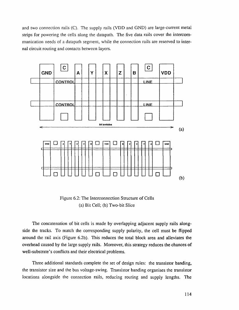
and two connection rails (C). The supply rails (VDD and GND) are large-current metal strips for powering the cells along the datapath. The five data rails cover the intercommunication needs of a datapath segment, while the connection rails are reserved to internal circuit routing and contacts between layers.
GNDC
A Y X Z BC
VDD
CONTROI 1 INF
CONTROL 1 INF
n n64 lam bdas
" (a)
Figure 6.2: The Interconnection Structure of Cells
(a) Bit Cell; (b) Two-bit Slice
The concatenation of bit cells is made by overlapping adjacent supply rails alongside the tracks. To match the corresponding supply polarity, the cell must be flipped around the rail axis (Figure 6.2b). This reduces the total block area and alleviates the overhead caused by the large supply rails. Moreover, this strategy reduces the chances of well-substrate’s conflicts and their electrical problems.
Three additional standards complete the set of design rules: the transistor banding, the transistor size and the bus voltage-swing. Transistor banding organises the transistor locations alongside the connection rails, reducing routing and supply lengths. The
114

transistor banding also contributed to the standardisation of transistor width in 4 lambdas. This small size for transistors leads to faster circuits by limiting the load of control drivers.
The voltage swing of signals that move data between resources in the datapath, affects the bus delay in proportion to the bus capacitance48. Bus precharging is a technique which reduces this problem and it is most useful in designs where the bus is idle every other phase or cycle due to the organisation of the processor62. For designs such as the Neural-RISC, in which the processor uses the bus on every clock phase, the limited voltage-swing bus48 is a more suitable approach. The use of this technique (granted by the NMOS pass transistors used as register access gates) required careful design and tests, and contributed to minimise the machine cycle time.
6.2.2. M odular Register Building Blocks
The main requirement in the storage cells design was to attain a flexible set of modules that could be assembled according to the desired functionality. To meet this requirement, we have designed a set of modular building blocks that can be assembled to create registers with the desired number of ports and reset/preset features.
The register building blocks were designed using the "ratioed" logic coupling technique for minimum area consumption116. With this approach, the register terminals can be accessed through pass-transistors, reducing considerably the necessary number of control lines. Actually, the use of "ratioed" logic halved the number of control lines, since
only one line is required for each pass-transistor, instead of the two as with the transmission gate. In addition, "ratioed" logic grants smaller machine cycles due to its intrinsic limited voltage for the level "one", caused by the pass-transistors48. The fundamental limitation in the "ratioed" logic technique is the asymmetry in the rise and fall timings.
The register building blocks can be classified into four categories: basic register, bus read and write, preset and reset and register-to-register connections cells.
Register Cells - The basic register design was centered on the semistatic (or pseudostatic) approach where the charge of the dynamic memory element is refreshed every cycle8 . The circuit shown in Figure 6.3 implements a bit storage with two inverters and two transmission gates. The transmission gates TGI and TG2 control the transmission and restore phases, respectively; the inverters provide complementary contents. For this
circuit, the input data in X is transmitted to the output terminal Y during <!>], and it is
115

restored back into the input stage during <t>2. With this scheme, it is possible to read and write a register in the same phase, by using a two-phase nonoverlapping clock.
writeo
bit-in
<D2
TG1
<D2
<D1
TG2<m
read1bit-out
Figure 6.3: Schematic of the basic register.
Input data as well as reset and preset commands are fed into the X terminal via pass transistors, making use of one control line per input (Figure 6.3). Likewise, the register’s output is read into the datapath buses (or into another register) through pass transistors. Care must be taken in order to prevent TG2 to be closed simultaneously with an input pass transistor, to avoid data conflict between an input data and the restored value.
This basic register has been developed using two different layout designs. The first layout provides access to the input/output terminals from both top and bottom cell boundaries. This feature permits direct data communication through the X and Y terminals, avoiding the unnecessary use of the common datapath buses. However, this cell is not transparent to bus Z, supplying terminals to buses A and B only. The second layout retains transparency to all three datapath buses A, B and Z but requires a larger area. Besides increasing the cell height, this configuration looses the access to X and Y terminals from one of the cell’s boundary (X and Y terminals are available at the top, while their complements are provided at the bottom of the cell). Although this feature can be view as a limitation, it is actually quite useful in cases where the previous and current cell’s output values are required simultaneously, or when a master-slave configuration is desired.
Buses Read and Write Cells - These cells comprise a single pass transistor which connects the X and Y terminals to one specific bus. A simple design has been achieved by selecting the "ratioed" logic coupling mechanism. These cells provide read and write
116

facilities to all existing buses, namely A, B and Z. Any combination of these buses can be used, allowing the basic register to have up to 3 bus ports.
Preset and Reset Cells - These are simple cells that provide the facility to force a specific value into the register. They are also implemented through pass transistors plugged into the register’s X terminal.
Register-to-Register Connections - To increase the register’s connectivity, two additional ports have been provided in the form of register-to-register connection cells. These cells contain one pass transistor that basically connects the X terminal of one register to the Y terminal of another register. The coupling can be made at the top and bottom boundaries of the register cell. Therefore, by coupling the appropriate building blocks, the basic register can communicate through up to 5 ports.
Single-bit modular register cells can be arranged into one datapath width module or can be split in fields with isolated bus accesses and reset/preset configurations. Apart form having up to 5 ports and reset/preset features, the basic register can perform extra functions with the addition of some functional elements such as counters, comparators and shifters.
6.2.3. Functional Elements
Functional elements are special cells designed essentially to provide extra functionality to the basic register. They include comparators, counters, shifters, and a general-purpose arithmetic and logic unit (ALU). All these functional cells can also be organised in fields of any length or even be mixed, in order to provide the necessary functionality to the datapath.
Comparators - The cell library provides a set of four different comparators to conform with the required number of ports and functionality. Their design follows the same approach used in the basic register: some comparators offer transparency for the two
basic datapath buses (A and B), while others include the bus Z terminal, but use a higher cell. The library also includes dedicated comparators that test registers contents, either to zero or all one values.
Comparators in the cell library adopt a single design strategy. Their common structure is based on the traditional exclusive-or (XOR) design, implemented with AND/OR gates. Smaller circuits could have been achieved by using the transmission gate XOR
117

logic132. However, switch level simulators such as Silos5, present problems with this design, hence the decision of not using it.
Counters - The counter cells supplied in the cell library were designed to easily integrate with the basic register. The register’s output is used as the counter’s input; after evaluating the new value the comparator directs the result to the register’s input. Three different configurations are supplied: an UP counter, a DOWN counter and a combination of both— an UP/DOWN counter.
The method adopted for the comparators design is based on an array of pass transistors, controlled by the register’s output. The counting is accomplished through a dual carry chain (the carry signal and its complement), similar to the one used in the ALU (see subsection Arithmetic & Logic Unit).
Shifters - The shifter functional element has also been specially designed to interface directly with the basic register. It is based on the barrel shifter approach82 and provides left and right shifting operations. Due to the register’s "ratioed" logic design, the basic shifter has been implemented using simple pass transistors to attain a smaller silicon area. To afford special facilities for arithmetic shifts as well as for shifting a concatenated register, specialised shift cells have also been designed.
Arithmetic & Logic Unit - For the ALU the important features are: the type of functions it can perform, the data width, and the operating speed. To support multiple VLSI projects, we have designed a general-purpose ALU, with a configurable width and an optimised carry chain. The structure of the ALU resembles that presented by Mead and Conway82, i.e., it contains: three logic function blocks for generating P (propagate), K (kill) and R (result) signals; and the carry chain circuit. These function blocks provide inputs for the carry chain and for the ALU output stage. Twelve control wires (four for each function generator) are used to select among the various logic functions of three variables (A, B and Carry).
The carry chain is typically the most speed-critical component in an ALU since it must take the carry information across the width of the ALU48. In the standard implementation of the Manchester carry chain, a single carry chain (usually, taking the
inverted carry signal) runs through a series of pass transistors with a precharge circuit at each stage. A pair of cascading inverters is inserted at regular intervals to overcome the quadratic delay originated by the series of pass transistors82. We have established a variety of the Manchester original design by adopting a dual carry chain with asynchronous charge. The circuit for one stage of the modified Manchester carry chain is shown
118
in Figure 6.4. The circuit activates the asynchronous charge by "generating" a carry. Thus, when P=K=0 (corresponding to the inputs A=B=l ) y carry lines are charged properly. The dashed lines represent how the carry chain is buffered: at restoring stages, an inverter is introduced in each chain and their outputs are interchanged between the two
chains.
VpD
p o-
Carry-inCarry-out
VDD
K° o<h Carry-inCarry-out
P°
carry chain bufferK°
Figure 6.4: Carry chain circuit for the ALU
The techniques used in this design serve a twofold purpose: they speed up the ALU operation and provide a design compatible with our strategy for machine timing. The
gain in performance is obtained by the use of a single inverter rather than two at each restoring stage, and by adopting asynchronous operation for the carry chain (instead of using a whole phase for precharging and the following phase for calculations, the ALU combines both operations concurrently in a full "shorter" cycle). This design uses more area than the single pre-charged chain, but it is justified to compensate the lack of lookahead circuitry.
119

An additional characteristic of the ALU allows writting the result of the ALU operation without consuming resources of the datapath. The ALU contains an internal path that takes its outputs back to its inputs location, so that it can be loaded into one of the feeding registers. This feature accounts for the overlapping of the instruction fetch and ALU
operations.
6.2.4. Interface and Switching Elements
Interface elements are cells designed to improve flexibility and compatibility among operative blocks. They include: bus drivers, data-alignment converters, and padding cells. Switching elements are simple arrays of pass transistors for interconnecting bus lines.
Bus Drivers - These are more complex interface cells, designed to match the electrical characteristics between internal and external buses. The bus drivers amplify the limited- driving signals of the register drivers and simultaneously convert them into full CMOS range. A bus driver has two stages: the first senses the ratioed levels; the second restores the signal level and supplies a fan-out sufficient to drive three standard cells. These drivers are designed in two types—unidirectional and bidirectional— and incorporate controls lines to put their outputs into high impedance.
Data-alignment Converters - These cells provide extra flexibility in the datapath design, by exchanging the topological assignment of buses for specialised connection. These converters transpose bus lines across bit boundaries, diverting the bus route. They are
used as barrel shifters, that shift bus lines in steps of n bits, aligning bytes packed in multi-field words.
Padding Cells - Padding cells are interface units, used to separate modules with incompatible borders. In the cell library, modules were designed to optimise the area used for each function. However, modules are conservative in respect to the margin to avoid border conflicts. The avoidance of all possible conflicts would excessively penalise silicon area, therefore a variety of padding cells were designed. These cells interface contiguous modules both, horizontally and vertically, interrupting the appropriate lines.
Switching Elements - These elements provide a simple gating to connect or isolate two buses under demand. No signal amplification is performed and the switching elements add their own load to the buses burden. These elements can substitute full tri-state buffers, in cases where minimum area is decisive. Switching elements are also applied to
120

provide pseudo-static storage in combinational circuits. For instance, they are positioned at the input of combinational PLAs to incorporate dynamic retention on the input lines. These elements do not comply with the topological standards of the other cells but, instead, they assume the characteristics of the external elements they connect.
6.3. Chip Organisation
6.3.1. Operative Part Organisation
The operative part of an integrated processor establishes the hardware implementation and the topological structure of the elements defined at the functional level. There are several criteria for the organisation of the operative part available to the machine designer20. Here, the design of the operative part is based on the principle of information locality for increased performance, with local memory and registers providing multiple accesses.
The Neural-RISC operative part is organised in five blocks: a two-segment datapath, the local memory, two I/O buffers, and the boot ROM (Figure 6.5).
The datapath occupies approximately 11.3% of the chip area. It has a structure which constitutes two perfect rectangles, with metal-1 buses and metal-2 control lines. This rectangular datapath is sliced and assembled from a large number of small cells on a multiple bus structure— a double bus on the right segment and triple bus on the left segment. The bus system is interrupted by sets of tri-state drivers which allow data transfer or independent processing by the operative sub-parts. These tri-state drivers are made
sufficiently large to drive the capacitive loads of internal and external buses lines, and to
convert the signal of the limited voltage-swing buses to a level accepted outside, by the standard cells and memory blocks. The whole datapath is 16-bit wide, although some
registers with fewer bits share horizontal slices, in order to reduce the height of the datapath.
Functionally, the datapath is composed of three operative sub-parts:
• Data processing
• I/O buffer management
• Communication processing
121

data addres:
Boot
ROM
I/O Buffer
data address
R AM
I/O Buffer
data address
R AM
Local Memory
data address
RAM
B A DR/B AR/A DUB AUA
Input LinkO utput LinkDR
A/AR/ALBUS A
x <
BUS B
DL
Input Link Output Link
v ------------Data Processing I/O Buffer
ManagementCommunication
Processing
Figure 6.5: Organisation of the Neural-RISC Operative Part
The data processing sub-part includes the execution unit and the timer (Figure 6.5). At the the right end of the first datapath segment are the registers and counters used for I/O buffer management. The second datapath segment (right side) contains the hardware (registers, latches, comparators, etc.) that implements the data ports and the input arbiter of the communication unit.
6.3.2. Control Part Organisation
The control part of a sequential machine drives the operative part by activating its control lines at the right time according to the system timing. The control part of the Neural-RISC takes less than 5% of the prototype chip area and it is implemented with
122

PLAs. Each PLA synthesizes a "nondeterministic" finite state machine-^9, in the sense that a machine can be in more than one state at the same time. The PLA implementation of nondeterministic finite automata112 provides a considerable reduction of silicon area, in contrast with conventional implementations96.
The organisation of the control part, shown in Figure 6.6, is extremely simple and includes three control units:
• Processor control unit
• Channel-R control unit
• Channel-L control unit
Processor Control Unit Communication Unit
PLA Channcl-R Channcl-L
PLA PLA
f 71o T
| 16O
p P 6I 1 o
Figure 6.6: Organisation of Neural-RISC Control Part
The processor control unit commands the functional components of the processor unit, i.e., the execution unit, the timer and the interrupt controller. The processor-unit PLA generates 21 different commands and takes 9 signals from the operative part, including a 4-bit instruction opcode. The simplicity of the instruction set allows instruction decoding and execution to be controlled by a single PLA.
The control units associated with the communication channels have identical PLAs that regulate the operations performed by the two communication engines. Each of these PLAs provides 16 control outputs and 8 input signals.
The system timing is based on two-phase nonoverlapping clock signals (4>i and <&2), generated directly by an external oscillator (Figure 6.7). Control operations are executed in a scheme where each clock phase corresponds to a conventional machine cycle. Instructions take an even number of clock phases and each of these phases holds a stable
123

state which is stored in static flip-flops. In the global control timing, a stable state is used to perform the equivalent to a full machine cycle, initiating and terminating transfers within the clock phase transition edges. This strategy accelerates the instruction flow, enabling instructions to execute in fewer clock cycles (Appendix 3 presents the control sequence of instructions). Compared with conventional designs, where states change every clock cycle, this design strategy allows distributing a slower clock over the circuit to attain the same performance. As a consequence of this approach, delays must be introduced to guard asynchronous sequential events from switching hazards. These delays are
physically dependent, and can induce failures on extreme operation conditions if careful inspection is not taken during design.
To achieve efficient utilisation of the cycle time, a pair of successive signals <J>i* and <&2x is generated internally from 0>i and 0 2 (Figure 6.7). They correspond to the two-phase clock signals with the nonoverlapping time equal zero. These extended-phase signals are used to command bus drivers and memory-address registers in order to speed up memory access. In these accesses, address decoding effectively initiates before the actual phase, when read or write operations occur.
Clock Cycle-£----------------- >-I I| Machine Cycles |r6 ^ ------ >■,
<e>i Lj _______
<J>2 — |_______ L_4i i i i
<£]* -----------I I
<t>2X ----------- ------------
Figure 6.7: Neural-RISC Clock System
This timing strategy applies to all control units that operate by sharing resources on alternative half cycle basis. Resources used by an unit in a phase are released to the use
124

of others in the consecutive phase. Resource alternation is a counter proposal for increasing the machine performance. Increased performance could also be obtained by doubling resources and by using complex self-synchronised control for resource contention. However, this approach would require far more silicon area. Instead, with the approach taken, silicon area is saved towards the integration of multiple processors in the same chip.
6.4. Implementation Considerations and Results
The major trend in the design effort has been focused on two implementation considerations: the optimised use of the silicon area for improving parallelism of integrated nodes; and a short implementation time, compatible with the project schedule. The composition of VLSI design tools used, allowed us to complete the chip design and to partially meet these consideration points. We experienced a number of difficult problems for not having used an integrated development system. It took longer than expected to produce the final layout and some planned tasks could not be executed. For instance, we produced a consistent functional specification for all cells and blocks in the layout design, that could later be used to run a functional test. However, the lack of functional models for nMOS and pMOS transistors in our version of the SOLO system, added to our limited time, prevented us from performing such test. Also, design tools provided insufficient support for layout measurements and therefore delivered poor statistics about performance and transistor count. Nevertheless, the automated place and route system played an important role for floor planning and area reduction.
We attempted several floor plane arrangements for different processor
configurations. We evaluated processors that contained IK, 512, 256, and 128 words of instruction and data RAM memory, and 64 and 128 words for the I/O buffer RAM
blocks. For each different design, a finished layout was produced and the chip area estimated for consistency with the maximum area admissible. The prototype was designed towards an academic multi-project service, with the maximum area limited to 100mm2, and integrated two complete microprocessors.
The floor plan used for the Neural-RISC prototype chip is shown in Figure 6.8.
The two microprocessors are symmetrically disposed along the longitudinal direction. The control part of both processors is aligned at the center of the chip, spanning control
signals to the left and right processors. The PLAs correspond to the Processor Control
125

L09 R09 R07 R02 R03 U 6
VSS I L08 I ROIO I ROI1 I ROftl VSS I R012 I R05 I R06 I U10 I VCC
66666 SAibdub b6hti5&U4 _ . Q
R13 _ Q
na- UR ill _ uL012___ £ - j
LOI4 |-~|
RIM _ Q
RI13 - - Q
RJ7
R It _ - Q
U31S _ Q
LQ13 - f a I
Lon—a L06 — -| I
TEST - f a I LOS - Q
LO« — - Q
RM — aL07 — - Q
L03 - - Q
•> - a
I/OBUFFER
I/O BUFFER
RAM
ROM
Data
Path
Data
Path
RCU1
LCU1
RCU2
LCU2
PU1
PU2
□ □
Data
Path
Data
Path
I/OBUFFER
I/OBUFFER
RAM
ROM
? o ? n ? n g n 9 n ? n m ?_VCC I RI101 R16 | RIO I U 15 | U13 | U1 | U 5
Q -Q -Q - 'D--D -a - 1
D -a -
a -a -
a -a -
a -a -
a -
a -a -
a -
a -
a -
a -
LI8
ROILCTSo
RJ2
RCTSo
LCTSi
U11
U 12
LX2
02
RCTSi
LRTSi
LOIO
SYNCL
LRTSo
OTRESET
RRTSi
L02
R19 JUS UM
U 9 | RolS I ROM
U 7 VCC RRTSo
Figure 6.8: Prototype Floor Plan
Unit (PUi), Channel-R Control Unit (RCU/), and Channel-L Control Unit (LCU/) of processor i. The areas between the PLA column and the datapaths contain standard cells that implement random-logic parts such as, the interrupt controller circuit, memory
decoding and control unit, flip-flops for storing the finite machine states, and so on. The upper segments of the datapaths correspond to circuits that implement data ports and input arbiters of the communication units, while the lower segments contain the processing units and the circuits for I/O buffer management. The memory blocks are laid close to the left and right borders of the frame.
The relative placement of the blocks attempts to minimise the distance between connecting terminals thus, reducing routing lengths and propagation delays. In addition, the assignment of position and direction of external terminals was controlled during the process of each block layout, in order to produce a more compact chip.
The prototype chip was implemented using 2p CMOS process technology with double-metal interconnection layers. The Neural-RISC features for this implementation
126

are summarised in Table 6.1. The chip contains about 60K transistors (the precise number of transistors could not be estimated), 891 standard cells, and 331 customised cells, in an 8.7mmx9.6mm die area. The total number of 84 pins includes 64 I/O data pins. The layout of the Neural-RISC prototype chip is shown in Figure 6.9.
Number of Processors Data Length Arithmetic Unit
ALU MULT
Instruction & Data RAM I/O Buffer RAM Boot ROM Control PLAs Machine Cycle Total I/O Bandwidth PackageNumber of standard gate cells Number o f full-custom cells Device technology Die Size
216-b
16-b1-b x l-b multiplication 128x l6 -b (per processor) two 32 x l6 -b (per processor) 3 2 x l6 -b (per processor)6100ns (estimated) 80M byte/s (estimated)84 pin CLCC8913312pm CMOS 8.7x9.6m m (84mm2)
Table 6.1: Prototype Neural-RISC Features
In the experimental evaluation for operation speed, the program SPICE was used to estimate the performance of possible critical paths in the processor’s circuit. One possible critical path is the long carry chain in the arithmetic logic. Its total delay corresponds to the delay of 4 cascaded inverters plus the delay generated by the series of 12 pass transistors. Another suspect path is associated with the register transfer operation, which
involves delays of the internal buses, the tri-state drivers and buses outside the datapath.
We observed the ALU operation for 16-bit data and the register transfer operation for worst case conditions. The simulation performed with SPICE showed that arithmetic operations (add and sub) can be carried out within 100ns. Since in the system timing the
ALU carry chain is allowed two phases to complete, this time corresponds to a close estimate for the machine cycle time.
For the register transfer operation, a pair of registers with full access to two buses were assembled together and tested. The buses were loaded with O.lpf to simulate the complete bus load. The test revealed that the pseudo-static registers can operate at frequencies over 20MHz, not establishing therefore a critical path.
127

7ir;in■ "V|HC»i.;r. i n , j j L y . A ^ ' r i l r n ^ ,.:- h u u j i ■
n m n '* rn in
E g
Figure 6.9: Neural-RISC Chip Layout

Chapter 7
Assessment
This chapter presents an assessment of the work performed in this thesis. It covers each of the main investigation aspects: the Neural-RISC system and node architectures, the architecture simulation and the VLSI implementation.The criteria used for the assessment consider the five design objectives, stated previously in Chapter 1, i.e., parallelism, performance, flexibility, architecture scalability and implementation cost.
7.1. Neural-RISC System Architecture
This section assesses the suitability of the Neural-RISC system architecture for its planned goals. As stated before, the original aim for the system architecture consisted of designing a parallel architecture to support in optimal fashion the massive parallel networking of neural nets. To this end, the system architecture should provide sufficient flexibility and expansion capacity for coping with a domain of applications and with general purpose experimentation. Additionally, a neurocomputer based in such architecture must prove to be practically feasible and cost-effective under the state-of-art technology and economic constraints.
To achieve these objectives, we have designed a highly parallel architecture which embodies a modular and hierarchical structure of the system components. In the Neural- RISC architecture, systems are constructed incrementally by bringing together chips, rings, and clusters of rings. Variable-length rings are built out of multiprocessor chips, connected in series through point-to-point parallel links. A programmable number of rings forms a cluster, with an independent interconnect module (MI module) to handle
the input and output of packets between processor rings. Clusters can be arranged virtually in any point-to-point structure, to meet the user requirements for system configuration. Such hierarchical structure provides the designer with a substantial degree of flexibility when building, reconfiguring, or expanding neurocomputer systems.
Systems can be expanded or configured using three alternative methods: increasing the size of rings, adding more rings to a cluster, or employing more clusters to build the main system. In this process, Neural-RISC chips are treated essentially as basic building
129

blocks that interconnect with minimum interface constraints, in a way similar to traditional RAM systems. When scaling the system architecture, the organisation of rings and clusters of rings allows the designer to achieve an optimal balance for performance and cost. For example, short rings distributed over many clusters favour system performance, while few clusters implemented with large rings reduce implementation cost.
A distinct feature of the Neural-RISC architecture is its ability to integrate a large number of processing nodes with no significant performance sacrifice. Systems with thousands of nodes are feasible, configurable and probably cheaper than many other neurocomputers of comparable power. On the other hand, systems with fewer processor
nodes, forming single board neurocomputers for low-end workstations or PCs, can also be created to meet the requirement of lower cost and lower performance applications.
The suitability of the Neural-RISC architecture for partitioning and mapping neural networks, can be intuitively seen from its topology (Figure 7.1 reproduces the diagram presented in Chapter 3). For many neural network applications, the Neural-RISC system architecture can achieve high performance by splitting up a neural network, one neuron node per processor. Alternatively, when memory requirement is low, a neural network can be virtually simulated, by mapping neuron nodes across the implemented processors. To support mapping neural networks, the message routing system provides simple and flexible mechanisms for numbering nodes and routing packets, well suited for neural nets.
The message routing system defines a packet switching procedure with asynchronous communication and distributed control of message routing. The system conforms with the communication structure of neural networks, characterised by a large number of virtual interconnections per node and small size of messages4 . For assisting a wide variety of neural models with different input/output constraints, the system employs programmable-size packets and supports virtual connections. Efficiency is tackled by a message routing system which favours localised communications and minimises the overhead for global communications— communication in a ring is carried out by forwarding packets, a word at a time, through opposite-direction channels; transferring packets between rings and between clusters of rings involves a single vertical step. Communications performance is further improved by providing support for an efficient mapping of neural networks.
The Neural-RISC architecture is amenable to simple mapping algorithms. To support the implementation of these algorithms, the message routing system provides a
130
o t d o W o o
0 ^ 0 ^ 0 : : : = 0
Layer 1
Layer 2
Cluster
*■<)—>
— ( )—>
\
o :
VirtualPF
VirtualPE
Virtualj- - P £ . j
Layer n
I I Neural-RISC £ ) Neuron _________ Virtual Processor Element Connection
Figure 7.1: Mapping of Neural Networks
network addressing scheme that minimises interprocessor communication. The network addressing scheme reflects the hierarchical structure typically present in neural networks. It supports four different programmable addresses (layer, cluster, node and global broadcast) for identifying destination processors in the system network. When layered neural networks are mapped onto the Neural-RISC system architecture, clusters of neuron nodes within the same layer are mapped on to nearby processors. Rings constitute the natural broadcast domains and, as such, they are suitable for implementing clusters and layers of neural processing elements (Figure 7.1). A cluster of rings may execute a complete neural network algorithm or a set of layers in a large neural network. The clustering of processors reduces the bandwidth demands of neural networks, bringing then to a manageable level. Selective broadcast communication reduces the number of transmissions from nodes with a large fan-out thus, improving performance significantly. The mapping and execution of neural network algorithms are the main targets of the routing
system but network control and monitoring operations may also make effective use of these addressing features.
131

The system provides support for implementing control and monitoring operations that are typically required by neural network programming systems. In performing these operations, control packets specifying exclusive virtual links, are exchanged between the host and the processor nodes. Control packets having different purposes, initiate a control operation at the processor nodes by means of virtual link numbers that point to
specific service routines. Certain control packets can be broadcasted to a group of nodes but others, either because of the nature of the operation or because of the volume of data returned, are restricted to specific nodes. At this stage perhaps the major deficiency of
the Neural-RISC system architecture in this area is the lack of a global broadcast bus for connecting processors directly to the host. Operations that require saving pertinent data within the network, including those for saving partially trained neural networks for later
processing, are poorly supported by the system architecture. The amount of data involved make these operations impractical. A global broadcast bus could solve this problem, with a unquestionable benefit for performance. However, it must be noted that, due to elementary physics limits, a single global broadcast bus can not support a large number of processors. Consequently, many buses would be needed to completely link the processors to the host. Such alternative would certainly impair the homogeneity of the communication plan and therefore, it was not implemented. At this point, it is worth mentioning that our option for a smoothly extensible, parallel system architecture is largely supported by recent studies performed as part of an IEEE standardisation project for a multiprocessor scalable interface^4,
7.2. Neural-RISC Node Architecture
In this section, we assess the effectiveness and the efficiency of the Neural-RISC node architecture as a building block for implementing a parallel general-purpose neuro- computer. The criteria for assessment consider the prescribed design objectives and also
the relevant attributes for node architecture, defined in Chapter 2 (i.e, capacity, accuracy and generality).
For the node architecture, an original goal was to achieve a rational balance between the contrasting issues of flexibility and performance. In terms of flexibility, a versatile node architecture must incorporate in silicon, adequate support for a set of elementary compute-intensive algorithmic operations, which are shared by all known neural models. As the variety of models can be created to a large extend, the node architecture must also provide comprehensive support to allow the porting of applications between
132

different neurocomputer systems. On the other hand, to attempt the high performance required by real-world applications, the node architecture must efficiently perform both, in terms of processing and communication speeds.
The Neural-RISC node architecture combines the issues of performance and flexibility, by integrating both the computation and communication functionalities into a single VLSI component. Each Neural-RISC node contains a processor unit and a doubleengine communication unit. The processor unit can carry out computations independently from the operations being performed at the communication unit. Indeed, many applications can completely overlap communications and processing, maximising overall system throughput. To relax the coupling between execution and communicating processes, the node architecture incorporates a flexible buffering mechanism that can be
sized according to the I/O requirements of neural network algorithms. The Neural-RISC provides the user with a circular FIFO buffer for input, and a memory buffer for output both, with programmable buffer areas. Two basic modes are available for controlling the I/O of packets: a polled mode and an interrupted-based mode. This flexibility yields benefits in execution efficiency for most of the neural network models which are known to perform input and output in a disciplined manner.
Our basic considerations in choosing an appropriate interconnection structure for the processors nodes have made us choosing parallelism as the primary goal. Consequently, we opted for the regular structure of the linear array as a way to achieve unlimited clustering capability for improving packing density. As the processors in a linear array are connected to both of their nearest neighbours, the communication unit provides bi-directional word-width communication ports on two sides. A high speed data transfer mechanism, implemented by triple-ported word-shift registers, allows the overlapping of the receipt of a data word from one neighbour processor with the transmission of the previous word to the next processor, in one single cycle. These features make efficient use of the data I/O pins (64) in support of low-latency neighbour communication and high I/O bandwidth through the processor array.
To evaluate the communication bandwidth, we take as example, the Neural-RISC VLSI prototype chip and the recently announced Transputer T9000^^. At this point, our
intention is not of comparing the Neural-RISC processor to the INMOS Transputer, but rather to assess the impact that parallel links have in the communication system performance. Using an outdated technology (2\i CMOS), the four 16-bit unidirectional links of a 10MHz Neural-RISC processor are expected to provide a total bandwidth of 80Mbytes/s. (This corresponds to the peak rate of 20Mbytes/s per link). The T9000,
133

operating at a clock speed of 50MHz and using a 100-Mbit/s link protocol (twice the input clock frequency), supports a 80Mbytes/s total bi-directional link bandwidth through four (bi-directional) serial communication links. (The maximum bandwidth is smaller when start and stop bits are considered). However, we must make a cautionary note about this analysis. Even though both processors exhibit similar bandwidth, the level of connectivity achieved by the four bi-directional links in the Transputer is considerably higher. Since a message needs to cross fewer intermediate nodes to reach its final destination, the overall system throughput with Transputers is superior. The idea therefore, is to compensate the low level of connectivity with the parallelism of the links and with mechanisms that reduce communication overheads.
A key goal in the design of the Neural-RISC processor was generality. This goal is reflected in the structure of the processor unit, the instruction set and in the specification of its functional units (i.e. the timer and the interrupt controller). The instruction set has been optimised for programming the simple algorithmic structure of neural models, either directly or by means of neural network description languages. In a large class of neural network models, a set of typical operations need to be programmed. Such operations take the form of arithmetic formulas whose general characteristic is illustrated in the Table 7.1.
Recal] Phase
Network activation Xi = Z Wij .y j- 0Threshold function n”55+i—H'w'
+II
Learning Phase
Error calculation z = t j -yjWeight updating AWij = T | .yt-
Table 7.1: General Characteristic of Neural Network Operations
As can be seen from these formulas, the functional complexity for either recall or learning is very low, multiplication and accumulation are the fundamental operations. Threshold functions, for involving somewhat complex operations, are typically implemented by look-up tables.
In the Neural-RISC processor, support for programming such operations observes a compromise between performance and silicon area. The instruction set includes a 16- cycle signed multiplication instruction, and an accumulator-indexed read instruction to optimise the access to tables that represent functions. Two’s complement signed
134

numbers are used for all arithmetic instructions; shifts also conform with this representation rule to assist in the fractional scaling of products. The remaining instructions were carefully defined in order to provide adequate support for general programming, and to improve code-density. The provision of these instructions fulfills the basic requirements of neural network description languages which can use the Neural-RISC processor as a target machine for running compiled code. The NIL compiler, written for the Neural- RISC processor, and the simulated benchmark neural algorithms (e.g., Hopfield, Back
Propagation and Kohonen’s feature map), coded into the NIL language, present current evidence of this assertion. In addition, these experiments showed that the capabilities of the instruction set in expressing and manipulating neural network values, satisfy the requirement of numerical accuracy.
The objective of high performance was attempted during all phases of the design using many different techniques. These include simple pipeline structures, multiported registers, simplified instruction format, and a special strategy for the machine control. As a result, most of the instructions (86%) are single cycle, which gives an average instruction execution time of 1.6 cycles. This rate is somewhat high when compared with other RISC machines. For instance, the Sparc SF9010IU has a rate of 1.3 cycles per instruction92. The main reason for this difference is that, RISC machines such as the Sparc, use involved pipeline structures. Another reason is the multiply instruction which contributes with 16 cycles in this rate. However, multiply represents a considerable improvement in performance for the execution of neural networks; its inclusion is justified if we consider that each incoming packet originates a multiply operation.
In RISC designs, the simplicity of the instruction format lends to a simplicity of the implementation62, allows shortening the execution time, and ultimately, determines the ease with which the instruction set can be extended in future generations. As noted previously, the encoding of the instructions in the Neural-RISC follows an extremely simple format (a 4-bit opcode and a 12-bit operand). With such a format, it becomes difficult to
expand the instruction set and to preserve the field boundaries for simple decoding. Although an immediate need for instruction set expansion has not been detected, such a contingency will result in awkward, longer decoding stage. In this respect, the Neural- RISC node architecture exhibits little flexibility and has not adhered to the principle of a scalable design; we believe that this was a bad design decision.
As noted in the literature survey, the capacity of a neurocomputer is determined by the node’s implemented memory, necessary to represent weighted connections, look-up tables and other values. For the Neural-RISC architecture the maximum implementable
135

memory, defined by the memory address space in direct mode, is 4K words (the actual implemented memory depends on the processing technology). One may argue that the Neural-RISC has low capacity for representing a neural processing element. In fact, the on-chip memory may constitute a limitation in applications that include: virtual processing elements; nodes with large fan-in or fan-out of weighted connections; the use of non-optimised compiled code; or that demand a large code for implementing control and monitoring routines. However, we rather consider the bound capacity not as a limitation
but as the price to pay by fine-grained parallel architectures, in favour of simplicity of system integration.
7.3. Architecture Simulation
This section evaluates the simulation studies regarding their effectiveness in supporting the design of the Neural-RISC architecture. As mentioned earlier, the primary objective of the simulation studies was to investigate design alternatives for the system and node architectures. To this end, three software simulators were produced and their code continuously revised during design and implementation of the Neural-RISC architecture.
The second important objective consisted of providing support for the development of a neural programming system (NPS) and a neural network implementation language (NIL), designed as part of another PhD project26. With this objective, we have established a collaborative work in the associated areas of research, which resulted in the development of a common simulation environment for executing neural network algorithms.
The software simulator, in its final version, takes 5000 lines of C code, distributed over five configurable modules, to realise all of the Neural-RISC system and node components. The simulator employs a register-transfer model and uses a global clock, in
units of mega hertz, to drive the concurrent events associated with each component. In addition, it includes an extensive user interface and general support for gathering statistic
information. The software simulator performs the whole neurocomputer and constitutes the core of the simulation environment.
The simulator environment integrates several software modules which entirely cover all steps in the process of programming and executing neural models. It constituted a considerable part of the simulation studies and demanded close co-operation for
136

designing and testing. For the sake of clarity, we reproduce in Figure 7.2, the internal structure of the simulation environment, presented in section 5.1.2. The simulation environment consists of:
Arch. Simulator:
Boot:
Service:
NIL Compiler:
Assembler:
Algorithms Library:
to simulate the neurocomputer in size and configuration as required by the applications.
the assembly code for the processors’ bootstrapping ROM.
the assembly code for implementing a standard set of I/O and interrupt service routines for the processor nodes.
to generate the processor’s assembly code, correspondent to the NIL source code.
to convert the assembly code into executable object code.
a set of standard models coded in NIL, comprising: Hopfield model, Backpropagation, Kohonen’s Feature Map, and Boltzmann machine.
Mapper: to map and load neuron nodes into the simulated processors.
AlgorithmsLibrary
S ' Input 'N
Service
Boot
H NPS3 »- Command Interpreter
Mapper <i
\
ArcKTi
- t i o o - t h
- D O O ' C h
ecture Simulator
Compiler
AssemblyProgram
Assembler
I Object \ V Code )
_ r
Figure 7.2: Simulation Environment
The Neural-RISC and NPS/NIL projects profited greatly from the programming and application experiences gained with the simulation environment. Simulations allowed us
137

to test the neurocomputer with practical applications and to evaluate the abilities of NIL
as a neural network description language.
As a vehicle for assessing a range of design choices, simulations proved to be very
effective, bringing relevant contributions to the Neural-RISC architecture. From the original specification, the node and system architectures assimilated a number of fundamental changes, before reaching the current version. For instance, in the system architecture, the topology of the interconnection plan evolved from a single linear array to a structure
composed of multiple rings. The node architecture started from a single-instruction processor and stepped into other intermediate instruction sets, before maturing with a 16 instruction set. For performing these changes, we analysed statistical records in two principal areas: the instruction set usage, based on the spectrum of instruction frequencies in the code generated by the NIL compiler; and the efficiency of the communication system, measured through the average traffic load, average packet delay, percentage of blocked links, and average I/O processing delay. In summary, simulations allow us to achieve the following improvements:
System Architecture
1* Introduce variable-length input (FIFO) queues for maximising communication throughput.
2. Redefine the topology of the system architecture and introduce multi-ring interconnect modules.
3* Improve network addressing scheme by including selective broadcast addresses.
4. Change the packet switching procedure for reducing packet delay.
Node Architecture
1. Improve the instruction set usability and efficiency by creating instructions such as MULT, GET, SANT and LDI.
2* Improve code density by introducing memory-mapped instructions.
3* Achieve an optimal dimensioning of the hardware associated with instructions.
4. Incorporate general support such as an interrupt controller and a timer.
5* Redesign the communication unit for reducing communication latency and for improving the coupling with the processor unit.
For pragmatic reasons, the model chosen for simulating the communication system provided only moderate accuracy for the evaluative measures. This simplification permitted us to assess the effectiveness of the architectural features in relatively short time,
138

according to the timetable constraints of the thesis. Nevertheless, simulations allowed us to detect physical bottlenecks and to effectively reduce overheads in the communication system.
The only major limitation of the simulation studies is with regard to the speed measurement of the neurocomputer, i.e., a rate of how fast it can process specific neural networks. The greatest difficult at this point was in simulating large neural network benchmarks and to achieve a reasonable balance between the computation time and data propagation time. We saw that, a thorough assessment of the neurocomputer speed (i.e., total number of connections updated per second), would require a more involved simulator, and research in areas of considerable complexity such as: system optimal size and configuration, mapping of neural models and load balance, and compiler optimisation. This list surpasses the scope of one project and might compromise the time needed for the VLSI implementation; therefore, these topics are left for future work (refer to section 8 .2).
7.4. VLSI Implementation
In this section, we assess the VLSI implementation of the Neural-RISC architecture for its prescribed goals. For this part of the thesis, the primary objective was to investigate the hardware complexity of the Neural-RISC node architecture. The node complexity is the chief measurement to determine the degree of real parallelism a neurocomputer can achieve in practical implementations. In this respect, node area and packing density
form the essential criteria for assessment. A second equally important objective was to demonstrate the Neural-RISC architecture in terms of the fundamental design attributes for general-purpose neurocomputer systems. These attributes include: the neurocomputer overall performance, design scalability, implementation cost and feasibility.
For the VLSI implementation, we have considered several design methodologies and have carefully evaluated their influence in all design attributes. Design effort has been concentrated on the requirements of minimum silicon area and high performance. To this end, we have designed a datapath cell library, which emphasizes modularity and flexibility, and attempts a rational balance for performance and silicon area.
The preliminary results from the Neural-RISC VLSI implementation are very encouraging. Despite the problems experienced with the VLSI tools and the use of 2p, CMOS processing technology, the Neural-RISC prototype chip integrates two complete
139

nodes in a 8.7x9.6mm die size. The chip is expected to operate at about 6 MIPS, with an I/O bandwidth of 80Mbytes/s, driven by a 10MHz clock. In this chip, local memory was reduced to allow for a multiple-node prototype, which could be used for statistical purposes.
Prototyping was essential for the architecture development. The VLSI prototype provided us realistic feedback about the constraints of the hardware implementation and allowed us to evaluate reimplementations of the Neural-RISC chip with denser technolo
gies.
The best method to assess the VLSI implementation is by performing a statistical analysis in order to determine the packing and performance capabilities of the Neural- RISC architecture. To perform such analysis, we consider the Neural-RISC architecture in two levels, chip level and system level.
Chip Level— for this level, we want to evaluate the packing density and operating speed of the Neural-RISC chip, when implemented with denser technologies.
System Level— at system level, the objective is to determine the system complexity (i.e., the amount of hardware required to build a neurocomputer system with a given capacity), and its correspondent performance.
Chip Level
To estimate the packing density and operation speed of integrated Neural-RISC nodes, we follow a five-step evaluation process:
Step 1: Based on the size of the 2-node prototype chip, we calculate the processors’ core area by subtracting the area of the I/O pad frame. The resulting area is then divided by two (the number of nodes), to obtain the core area of one Neural-RISC node.
Step 2: In this step, we try to exclude the effect of using standard cells for the random logic design, in a way that the estimated area conforms with that of a full-custom design.
Step 3: Next, in order to consider nodes with various (real) sizes of local memory, we first take the node area obtained in step 2, and subtract the RAM area of the prototype chip. The core area for various Neural-RISC nodes with different local memories, is then calculated by adding the corresponding RAM area to the node area.
Step 4: Here, we determine the packing density (expressed in number of integrated nodes per chip) for the range 2.0\i to 0.8|i CMOS feature sizes. In view of current technology, a 150mm2 die is assumed. In these calculations, we utilise the area scaling factor 1/a2, where 1/a is the dimension scale factor.
140

Step 5: Finally, for the same range of CMOS feature sizes, we evaluate the maximum clock frequency and the node performance, i.e., the I/O bandwidth and the processors’ MIPS rate (millions of instructions per second). For this analysis, we apply the gate delay scaling factor, 1/a, to the performance rates obtained in chapter 6.
Measurements in all these steps were rigorously performed in order to provide a consistent assessment. The next four paragraphs explain the assumptions we have made
during the evaluation process.
1— Pad size is usually defined by the minimum size to which a bond wire can be attached132. Therefore, the actual size of I/O pads is not expected to vary substantially
with the scale-down of the processing technology. Since the Neural-RISC architecture allows implementation with no change in the chip pin-out (84 pins), it makes sense to consider the area of the I/O frame, constant for the same die size, in all technologies.
2— Standard cells have a significant impact on the core area both, because of the size of the cells and also because of the routing area required. We have estimated the effect of standard cells during the design of a toy microprocessor, implemented as part of the evaluative analysis of VLSI tools (refer to section 6.1). We saw that, the use of full custom cells for random logic could reduce the total node layout area in at least 15%. Accordingly, the node core was recalculated.
3— RAM blocks have their areas automatically calculated by a RAM generator. Although the generator does not employ an optimised RAM design, it provides the necessary precision for a more conservative analysis.
A— The model we used for scaling is based on the simple first-order MOS scaling theory132. According to this model, as we scale device dimensions by 1/a, circuit density scales up by a2, and the system’s clock period, for being proportional to the gate delay82, is shortened by a. Although it is unlikely that CMOS processing will scale in such a simple fashion, the results presented provide a reasonable idea as to what we can expect from the Neural-RISC packing density and performance as processes are scaled.
To demonstrate performance and packing capabilities of the Neural-RISC architecture, we take node examples with balanced configurations for local memory. Table 7.2 presents these Neural-RISC nodes and their correspondent complexity, expressed in mega X2 area units. Node configurations cover a range, from the minimum workable local memory (IK), to the maximum implementable instruction&data memory, 4K. (Note that, the I/O buffer memory can still be extended in all configurations).
141

Configuration Inst. & Data M em ory I/O Buffer Node Com plexity
N ode o k 4 K x l6 - b two 2 5 6 x l6 - b 133.6 MX2Nodei.sx 3 K x l6 -b t w o 2 5 6 x l6 - b 108.8 Mk2N0 d e 2.sK 2 K x l6 -b t w o 2 5 6 x l6 - b 84.1 MX2N o d e h2sK________________ !K x l6 - b __________ two 128x16-b 53.3 MX2
Table 7.2: Neural-RISC Node Configurations
Figure 7.3 depicts the curves of packing density (number of integrated nodes)
versus node complexity (node area in the technology length unit, Mk2), for a range of
CM OS processing technologies (2.Op to 0.8p). These packing statistics are summarised,
together with the performance statistics, in Table 7.3.
Number of Integrated Nodes
1716151413121 110
987654321
"N ode 1.25'0.8 microns
1.0 microns
"Node 2.5“' 1.2 microns
‘Node 3.5' 1.5 micronsNode 4.5’
2.0 microns
20 40 60 80 100 120 140 160
Node Complexity
Figure 7.3: Packing Density of Neural-RISC nodes
(N odes integrated in a 150 m m 2, 84-pin CM OS device)
As shown by these results, N ode\25K yields good packing density in most o f the
technologies, except 2p. On the other hand, Node^.sK only achieves good density (6
nodes) with the 0.8p process. In this case, a single chip can integrate six 16-bit proces
sors, each with its own 4-link parallel communication unit and 9K bytes of local
memory. However, with the 2p process (the m inim um feature size supported by the
142

academic multi-project service, by the time we started the VLSI implementation), only a
single N 0 d e 4 .SK can be integrated. Overall, low packing density is obtained for processing technologies from 2|i to 1.2p, while a satisfactory number of integrated nodes is achieved for the current most advanced technologies (i.e., 1.0)1 and 0.8ji).
It should be noted that, if a state-of-art RAM had been used in this analysis, the maximum number of processors per chip would have increased significantly. The reason
is that local memory occupies between 62% (N o d e \.25K ) and 85% (N 0 d e 4 .SK) of the total silicon area.
Technology 2p 1.5p 1.2p l p 0.8)1Packing D ensity
N0 d e 4 .sK 1 1 2 4 6N0 d e 3.SK 1 2 3 5 7N0 d e 2.SK 1 2 4 6 10N ode\.2SK 2 4 7 10 16
Perform ance
Clock speed (MHz) 10 13.3 16.6 20 25Processing (MIPS) 6 8 10 12 15I/O Bandwidth (Mbytes/s) 80 106 133 160 200
Table 7.3: Summary of Packing and Performance Statistics (Nodes integrated in a 150 m m 2, 84-pin CMOS device)
The performance of each Neural-RISC chip is presented in terms of its processing and communication efficiency in Table 7.3. The clock rate (expressed in mega hertz) indicates the chip operating speed, while processing performance (in MIPS) is the
estimated performance of each integrated processor node. The I/O bandwidth represents the total bidirectional bandwidth of a Neural-RISC processor through its four 16-bit links.
We find the performance results, in a way, very conservative for all technologies. For instance, the clock speed of 25MHz (0.8|1 process) is in accordance with the currently available microprocessors, but can be considered somewhat low, given the design simplicity of the Neural-RISC microprocessor. To achieve a higher operating speed for the Neural-RISC chip, the only alternative is a complete redesign and layout, with more advanced techniques. However, a doubled I/O bandwidth can be achieved by simply doubling the width of the communication links (32-bit links can provide
400Mbytes/s for the 0.8|i Neural-RISC processor). If such change was made, the chip
pin count would be 148 pins, still under the current technology limits.
143

System Level
Now, let us look at the hardware complexity for building neurocomputer systems from Neural-RISC chips, and at their overall performance. For hardware complexity, we would like to evaluate general packing and integration requirements such as the number of chips, number of boards, and number of MI modules for neurocomputer systems with
different sizes. For performance, besides the MIPS rate, it is meaningful including the system’s memory capacity, since an efficient neural network simulation requires balanced computational resources.
To determine the hardware complexity, we make some assumptions for the chip, board, and cluster subsystem levels of integration.
Chip: We consider the 84-pin (150 mm2) chips, fabricated in the 0.8ji CMOS process, in
four configurations (N 0 d e 4 .SK, N 0 d e 3.sK, N 0 d e 2 .SK and N o d e \ .25K ), as presented in Table 7.3. The number of integrated processor nodes per chip, considered for this analysis are 6, 7, 10 and 16, respectively.
Board: We use the IEEE standard board specifications for multiprocessor architectures-^, and adopt a triple height (366.7 mm), full depth (400 mm) Eurocard, which corresponds to a conventional Sun VME board. To calculate the circuit density at the board level, we make the following assumptions for placing the components: chips are housed in 84-pin CLCC (ceramic leadless chip carrier) package and plug to the board through a corresponding 84 lead chip carrier socket; for maximum board density, six- layer printed circuit boards (one for each chip side plus two for power supply) are used. Therefore, one board, in its effective area for printed circuits (355.6x393.67mm), can accommodate the maximum of 87 Neural-RISC chips.
Cluster Subsystem: We consider three possible topologies for cluster subsystems. Each of these configurations includes r rings of n processors nodes, connected to a multi-ring interconnect module (MI). With the three examples below, we try to visualise the system complexity in the spectrum of high performance (short rings) and low cost (long rings) neurocomputer systems.
R ingxNodes C haracteristic N odes/M l m odule16x3216x6432x128
high performance balanced low cost
12810244096
144

For this statistical analysis, we consider neurocomputer systems with IK, 4K, 8K, 16K, 32K and 64K processor nodes. (Here, "K" stands for 1024. Thus 64K means 65,536 nodes; 16K means 32,768, and so on). Statistics are presented in two parts: hardware requirements and systems’ performance.
Hardware Requirements. Figure 7.4 presents the number of chips and number of boards required to implement several neurocomputer systems with different Neural-RISC nodes. As seen from these graphs, the hardware complexity of the neurocomputer systems increases in consequence of larger integrated memory per node. The increase however is in a rate inferior to that of the integrated memory. For instance, N0 de4.SK integrates 3.6 times more memory than Node \.2sk but, the number of chips necessary to
built machines with N0 de4.sK is only 2.7 greater than that needed by Node\2 SK. This is because packing density also incorporates the node core area, which is constant (20 MA2) for any node configuration.
The high packing density of N o d e \ .2 5 K is reflected in its low hardware demands: a 1024-processor neurocomputer, containing 64 Neural-RISC chips, fits in one single Sun VME board, while a 64K-processor system needs 48 boards to mount 4096 chips. However, the hardware savings of N o d e \ .2 S K is not commensurate with the lower memory capacity (maximum of 160 Mbytes with the 64K-processor neurocomputer) as compared with N 0 d e 4 .S K . With regard to N 0 d e 4 .S K , hardware complexity only becomes significant for the 64K-processor system, which provides 576 Mbytes of memory (Table 7.5). This machine comprises 10923 Neural-RISC chips and clearly will require its own server chassis to accommodate 126 printed circuit boards. Nevertheless, for more compact neurocomputer systems, N 0 d e 4 .S K can provide up to 2048 processors embedded in a single Sun workstation, yielding 30 BIPS and integrating 18 Mbytes of memory. In the case of
N 0 d e 2 .S K and N o d e s . s K , practical implementation is obtained for all systems sizes.
Best results for hardware requirements can be obtained by using surface mounted devices. Overall, board density improves in the order of 78%, when sockets are eliminated. For instance, in the case of the 64K-processor neurocomputer, implemented with
N 0 d e 4 . S K , the number of printed circuit boards would fall from 128 to approximately 70.
The number of Multi-ring Interconnect modules for each neurocomputer system varies largely, according to the requirements of cost and performance (Table 7.4). For instance, using a very cheap configuration (32 rings of 128 processors each), a single MI module can handle 4096 processors, while 16 modules can configure a fully implemented, 64K-node, neurocomputer. On the other hand, to attain the communication
145

Number of Chips
64K NodesN ode 4 .5N ode 3 .5
•Node 2.5.10000 32K NodesN ode
16K Nodes1000
8K Nodes100
4K Nodes
10K Nodes
160120 140100806020 40
Node Complexity
Number of Boards
140130120
64K nodes•+ N ode 4 .5
32K nodes.+ N ode 3.5
10016K nodes
7060 8K nodes
+ N ode 1.254K nodes40
20 1K nodes
160140100 1208020 40 60
Node Complexity
Figure 7.4: Hardware Requirements for Neural-RISC Neurocomputers(a) Num ber o f Chips versus Node Complexity (in M X 2);
(b) Num ber of Boards versus Node Complexity (in M X 2);
efficiency provided by the 16x32 multi-ring topology, a total o f 128 MI modules are
needed. As described in Chapter 3, MI modules are autonomous units, containing a
146

standard microprocessor (i.e., an Intel 80xxx or a Motorola 680xx) which implements a number of I/O ports. Hardware requirements for these modules will certainly add to the neurocomputer complexity but, since their design have not been attempted in this work, we prefer not to assess them in detail. However, given the simplicity of a MI module, we believe that a single Eurocard can house at least sixteen of these modules.
N eurocom puter System IK 4K 8K 16K 32K 64K
Number o f MI modules for r x n clusters:
32x128 (low cost) 1 1 2 4 8 1616x64 (balanced) 1 4 8 16 32 6416x32 (high performance) 2 8 16 32 64 128
Table 7.4: Requirements of Multi-Ring Interconnect Modules
Performance. Table 7.5 presents the estimated peak performance and the memory capacity for neurocomputers implemented with different Neural-RISC nodes.
N eurocom puter System IK 4K 8K 16K 32 64K
Node\2 SKSystem memory (in Mbytes) 2.5 10 20 40 80 160
/Vo d e 2.5K
System memory (in Mbytes) 5 20 40 80 160 320
N 0 d e 3 .sK
System memory (in Mbytes) 7 28 56 112 224 448
N 0 d e 4 .SK
System memory (in Mbytes) 9 36 72 144 288 576
Peak Performance (in BIPS) 15 30 122 245 491 983
Table 7.5: Performance of Neural-RISC Systems
The performance of these neurocomputer systems is shown in "billions of instructions per second", while memory is presented in mega bytes. These performance figures look rather impressive at a first inspection, and should be considered with the appropriate
caution. The numbers reflect the machines’ peak performance, when all processors are
147

operating in parallel. In other words, when rc-K processors are operating concurrently, each executing a 16-bit instruction, the neurocomputer operates at about «x l024xl5 MIPS (15 MIPS is the estimated performance for the 0.8|i Neural-RISC processor). Although our intention is to illustrate the performance achieved by the massive parallelism of processing nodes, such results help to reveal the design space for the Neural-RISC architecture in neural computing.
148

Chapter 8
Conclusion & Future Work
This final chapter presents general conclusions, summarises results and contributions o f this research, and outlines ongoing work and potential future work.
8.1. Summary
The primary goal of this thesis was to investigate a RISC microprocessor and a parallel architecture for building a general-purpose neurocomputer. The motivation for the Neural-RISC node and system architectures was to develop a cost-effective hardware, suitable for supporting a range of neural network algorithms and to work cooperatively with existing neural network programming systems. The architecture objectives were parallelism, flexibility, performance, low cost, scalability, and the ease of system integration. Characteristically, some of these objectives often conflict. The Neural-RISC architecture is the result of a set of rational compromises that were made in attaining these objectives.
The Neural-RISC architecture has demonstrated the feasibility of programmable, massively parallel (fully) general-purpose neurocomputers. Its design trades off speed for flexibility, and some storage capacity for simplicity of system integration. The programmability of the node architecture and the flexibility of the system architecture can provide effective support for emulating any known neural network algorithm and for assisting the rapid transition of the neural network research field. The effectiveness of
the Neural-RISC architecture results from a balanced effort in the design, simulation, and
VLSI implementation of the architecture.
The Neural-RISC microprocessor approaches the processing and communication speeds necessary for solving large applications, while retaining the flexibility required for
supporting neural network environments. This flexibility yields benefits in the execution efficiency of neural models and in the density achievable in large systems. The parsimony of the Neural-RISC design allows, for instance, 1024 processor nodes, each provided with 9K bytes of local memory, to be packed onto two Sun VME cards. Such a
149

system can deliver 15 billion instruction per second peak performance, competitive with many current neurocomputers on a broad variety of neural network applications.
The system architecture defines a class of interconnect networks for modular construction of massively parallel neurocomputers. In particular, because of its cluster- based hierarchical structure, distributed control, and its expansion capability with no
significant loss of performance, the Neural-RISC system architecture offers an effective alternative for fast simulation of neural networks. The simple linear topology of the Neural-RISC arrays achieves practical implementations of complete systems; a special network addressing scheme naturally supports several neural network mapping algorithms, and compensates for the lack of higher dimensional connectivity.
Simulation helped us to focus on the architectural requirements and provided early feedback for different design alternatives. Notably, the development of a compiler was essential in designing and implementing the processor architecture. The design of the NIL compiler2 required a systematic study of the functionality of the Neural-RISC processor; this study permitted us to locate problems that might otherwise be undetected by
writing sample programs.
The VLSI implementation demonstrated the system and node architectures, and allowed us to assess the hardware requirements and performance of neurocomputer systems based on the Neural-RISC architecture. This assessment takes the form of graphs that picture these attributes for a spectrum of neurocomputer systems, implemented with state-of-art technology chips. Considering the limited experience and manpower available for the VLSI design (aggravated by the lack of an optimal set of CAD tools), much of the design effort was directed towards attaining a deliverable prototype in due course. We therefore believe that the next chip will be much closer to our goals.
While current understanding of neural computing may be insufficient to successfully construct a general-purpose neurocomputer, this thesis has demonstrated that a programmable RISC microprocessor and a simple parallel architecture, can be very effective when enhanced with mechanisms for supporting neural networks. It is unquestionable that any programmable neurocomputer is still an order-of-magnitude slower than what could be achieved by directly implementing a neural network with dedicated
hardware. However, flexibility is essential for research and for many applications, in a
field with the potential of neural networks. The Neural-RISC architecture represents a step towards this exciting prospect of constructing programmable neurocomputer systems, in a way analogous to other existing computing paradigms.
150

The contributions of this work to the neural network computing research draw toward other specific fields of research such as, parallel computer architectures, RISC
architectures, and VLSI design. Contributions have also occurred in the form of published work101*102’122, and as support to other PhD projects26’ 5 (refer to Chapter 1). Significantly, this thesis has provided a common focus for a large research project in neural computing. The work now forms the core of a multi-national project involving the University College London and the Brazilian University PUC/RJ. The main objectives of this project are summarised in this final section.
8.2. Future Work
Regarding future work, there is a number of tasks still to be carried out. Some of the more interesting ones will be attempted in a bilateral collaborative project, recently approved. The project, funded by the British Council and CNPq (Brazilian National Research Council), runs for three years and involves a significant amount of research and development to implement a general purpose neurocomputer system, based on the Neural-RISC architecture. The objectives of this project and its main tasks are described below.
The primary objective of this project is to construct a highly parallel computational system for supporting the simulation of neural networks and their applications. The project encompasses three main components:
1. the development of a general-purpose neurocomputer based on the Neural-RISC architecture;
2. the implementation of a neural network programming environment, targeted at the general-purpose neurocomputer, for developing and porting applications; and,
3. the development of an application to demonstrate the capabilities of the hardware and software of the neurocomputer system.
These three components of the research project will provide a comprehensive platform for neural network research and application. Additionally, on completion of the development phase, an extensive analytical evaluation of the neurocomputer system will begin. From this analysis, it is expected that comparative studies will be carried out to determine factors such as:
151
. the performance metrics of specific applications, in particular for those that demand high processing speed such as speech recognition;
• the applicability of the neurocomputer system both, as a research tool and as a commercial product; and,
• most importantly, its general performance, when compared with other neurocom
puter systems.
Regarding the general-purpose neurocomputer, the current VLSI implementation will be the basis for a new implementation of the Neural-RISC chip, using 1.2(I CMOS technology (currently the minimum feature size available in the academic multi-project service). When scaling down the chip layout to obey the design rules of the 1.2|i technology, this second silicon implementation will offer us a prime chance to evaluate the scalability of the VLSI design, by checking its results against the ones estimated in chapter 7 for this processing technology.
The opportunity of reimplementing the Neural-RISC chip with a more advanced technology, will also be beneficial for optimising some parts of the microprocessor design. Basically, we will look at improvements in the control of the communication unit and at the hardware necessary to introduce the divide instruction, which is useful in some neural network algorithms61.
The development of the general-purpose neurocomputer will also require additional work, not executed in this thesis. This work basically involves implementing the hardware of the multi-ring interconnect module (MI) and the software that performs at the host computer. The host will consist of a Sun workstation, while the MI module will consist of a standalone MC68020 microprocessor. Integration of the neurocomputer into
Unix as an attached processor will make the machine easily accessible to users and will permit supporting the programming environment.
The neural network programming environment will be built upon the Pygmalion environment, developed at UCL. In addition to Pygmalion, the environment will encompass parallel neurocomputer systems (in particular the general-purpose neurocomputer), a new set of commands for initialisation, control and monitoring of the parallel network
(see section 3.3.2), and ultimately, a supplement to the Pygmalion algorithm library, with
models used for speech recognition problems. Examples of these models are: Time Delay Multilayer Perceptrons77, Recurrent Backpropagation model61, and others8®.
152

As seen in chapter 2, the Pygmalion environment embodies an intermediate-level language nC (a C data structure) and a high level language N (based on C++), for describing neural network models. Integrating the general-purpose neurocomputer and the programming environment will require writing a nC compiler for the Neural-RISC processor. This way, neural network algorithms developed in N, can be translated to nC, and finally compiled and mapped onto Neural-RISC clusters. This second compiler, written for the Neural-RISC processor, will provide us further evaluation of its capabilities in supporting neural network description languages. At this stage, it is expected some exploratory work in compiler optimisation for reducing code size and execution
time.
Overall, the development of the programming environment will allow us: to evaluate memory requirements for codes compiled from higher level languages such as C; to test the Neural-RISC architecture with real control and monitoring operations; to obtain speed measurements of the neurocomputer, i.e., its CPS rate (connections per second) for various benchmarks.
The application has as primary objective, to consolidate the project and to demonstrate its efficiency and application. The proposal is to look at the performance of the Neural-RISC architecture in highly speed-demanding applications such as speech recognition. Initially, we plan to apply the neurocomputer system to the basic operations of speech recognition systems that include: pattern matching and classification, and time alignment and classification of input pattern sequences.
In addition to the continued development and evolution of the Neural-RISC architecture, the research project will involve a series of correlated studies not addressed in this thesis. Initially these studies include:
• mapping algorithms of neural networks to minimise communication overhead;
• optimal size and configuration of the neurocomputer system for different neural network topologies; and,
• capabilities of the Neural-RISC architecture for simulating virtual neural networks.
153

References
1. Praxis Systems, “ The ELLA Tutorial,” Issue 2.0, Praxis Systems pic, 1986.
2. ES2-European Silicon Structures, “ SOLO 2000,” Product Information, ES2, Germ- ering, West Germany, 1987.
3. IEEE, “ IEEE Standard for Mechanical Core Specifications for Microcomputers,” ANSI/IEEE std 1101-1986, IEEE, 1987.
4. Thinking Machines, “ Connection Machine Model CM-2,” Technical Summary HA87-4, Thinking Machines Corp., April 1987.
5. SDA Systems, Inc., “Design Framework; Automatic Place and Route; Design Analysis (Vol. 1 and 2); Design Entry; SDA Language; Physical Design and Verification,” Reference Manuals, Silicon Design Automation Inc., 1988.
6. IEEE, “ IEEE Standard Backplane Bus Specification for Multiprocessor Architectures: Futurebus,” ANSI/IEEE std 896.1-1986, IEEE, 1988.
7. MIT Lincoln Labs., DARPA Neural Network Study, AFCEA International Press, Lexington, MA, July 1988.
8. SAIC, “ DELTA/SIGMA/ANSim, editorial,” Neurocomputers, vol. 2, no. 1, 1988.
9. Meiko Scientific, “ In Sun Computing Surface,” Product Information, Meiko Scientific Ltd, Bristol, UK, 1989.
10. Adaptive Solutions, “ CNAPS Neurocomputing,” Product Information, Adaptive Solutions Inc., Beaverton, Oregon, 1991.
11. Agranat, A.J., Neugebauer, C.F., and Yariv, A., “ A CCD Based Neural Network Integrated Circuit with 64K Analog Programmable Synapses,” Proc. IEEE Int. Conf. on Neural Networks, vol. II, pp. 551-555, 1990.
12. Agrawal, D.P., Janakiram, V.K., and Pathak, G.C., “ Evaluating the performance of multi-computer configurations,” IEEE Computer, no. 19, pp. 23-37, May 1986.
13. Ahuja, V., Design and Analysis of Computer Communication Networks, McGraw- Hill, Singapore, 1987.
14. Aleksander, I., Thomas, W.V., and Bowden, P.A., “ WISARD - A radical step forward in image recognition,” Sensor Review, pp. 120-124, July 1984.
15. Aleksander, I. and Morton, H., Introduction to Neural Computing, North Oxford Press, 1989.
16. Alippi, C., “ Weight Representation and Network Complexity Reduction in the Digital VLSI Implementation of Neural Networks,” Research Report RN/91/22, Dept. Computer Science, University College London, 1991.
154

17. Alippi, C. and Nigri, M., “ Hardware Requirements for Digital VLSI Implementation of Neural Networks,” IJCNN’91 - Int. Joint Conf. on Neural Networks (to appear), Singapore, November 1991.
18. Alspector, J.A. et al., “ A Neuromorphic VLSI Learning System,” Proc. o f the 1987 Stanford Conf., Advanced Research in VLSI, pp. 313-349, 1987.
19. Alsup, M., “ Motorola’s 88000 Family Architecture,” IEEE Micro, vol. 10, no. 3, pp. 48-66, June 1990.
20. Anceau, F., The Architecture of Micro-Processors, Addison-Wesley, UK, 1986.
21. Angeniol, B., “ Pygmalion: ESPRIT II Project 2059, Neurocomputing,” IEEE Micro, vol. 10, no. 6, pp. 8-27, December 1990.
22. Arima, Y., Mashiko, K., Okada, K., Yamada, T., Maeda, A., Notani, H., Kondoh, H., and Kayano, S., “ A 336-Neuron 28K-Synapse Self-Learning Neural Network Chip with Branch-Neuron-Unit Architecture,” IEEE Int. Solid-State Circuits Conference,p. 182, 1991.
23. Azaria, H. and Tabak, D., “ The MODHEL Microcomputer for RISCS Study,” Microprocessing and Microprogramming, vol. 12, pp. 199-205, North-Holland, 1983.
24. Bahr, C. and Hammerstrom, D., “ ANNE (Another Neural Network Emulator),” Intel iPSC User’s Group Library, 1988.
25. Bavan, A.S., “ NIL-PLUS: A Neural Network Implementation Language,” Proc. Neural Computing Meeting, The Institute of Physics, pp. 171-178, London, April 1989.
26. Bavan, A.S., “ Neural Network Programming and Portability,” PhD Thesis, Dept. Computer Science, University College London, University London, August 1991.
27. Boser, B.E. and Sackinger, E., “An Analog Neural Network Processor with Programmable Network Topology,” IEEE Int. Solid-State Circuits Conference, p. 184, 1991.
28. Brown, N.H. Jr., “ Neural Network Implementation Approaches for the Connection Machine,” in Neural Information Processing Systems, ed. D.Z. Anderson, American Institute of Physics, New York, 1988.
29. Card, H.C. and Moore, W.R., “ VLSI Devices and Circuits for Neural Networks,” International Journal o f Neural Systems, vol. 1, no. 2, pp. 149-165, 1989.
30. Carlson, R. O. and Neugebauer, C A., “ Future Trends in Wafer Scale Integration,” Proceedings of IEEE, vol. 74, no. 12, pp. 1741-1752, December 1986.
31. Cleary, J.G., “ A Simple VLSI Connectionist Architecture,” Proc. IEEE First Int. Conf. on Neural Networks, pp. III-419-426, June 1987.
155
32. Cruz, C.A., Hanson, W.A., and Tam, J.Y., “ Neural Network Emulation Hardware Design Considerations,” Proc. IEEE First Int. Conf. on Neural Networks, pp. III- 427-434, June 1987.
33. Delgado, J.C., “ Parallel Computer Systems for Integrated Symbolic and Numeric Processing (SPAN),” ESPRIT Project 1588 Technical Report, November 1987.
34. Denker, J.S. and Wittner, B.S, “ Network Generality, Training Required and Precision Required,” IEEE Conf. on Neural Information Processing Systems - natural and synthetic, November 1987.
35. Duranton, M., Sirat, J.A., and Mauduit, N., “ Learning on VLSI: A General-Purpose Digital Neurochip,” Philips Journal of Research, vol. 45, no. 1, pp. 1-17, 1990.
36. Ernst, H.P., Mokry, B., and Schreter, Z., “A Transputer Based General Simulator for Connectionist Models,” in Parallel Processing in Neural Systems and Computers, ed. G. Hauske, Elsevier Science Publishers (North-Holland), 1990.
37. Fanty, M., “ A Connectionist Simulator for the BBN Butterfly Multiprocessor,” Butterfly Project Report, vol. 2, Comp. Science Depart., University o f Rochester, Rochester, January 1986.
38. Feldman, J. and Ballard, D., “ Connectionist Models and Their Properties,” Cognitive Science, pp. 205-254, March 1982.
39. Floyd, R.W. and Ullman, J.D., “The Compilation of Regular Expressions into Integrated Circuits,” Report STAN-CS-80-798, Computer Science Department, Stanford University, April 1980.
40. Foo, S.Y. and Takefuji, Y., “ Databases and Cell-Selection Algorithms for VLSI Cell Libraries,” IEEE Computer, vol. 23, no. 2, pp. 18-30, February 1990.
41. Forrest, B.M., Roweth, D., Stroud, N., Walllace, D.J., and Wilson, G.V., “ Implementing Neural Network Models on Parallel Computers,” The Computer Journal, vol. 30, no. 5, pp. 413-419, 1987.
42. Frank, E.H., “ A data-driven multiprocessor for switch-level simulation of VLSI circuits,” PhD Thesis, Carnegie-Mellon University, CMU-CS-85-185, November1985.
43. Frohman-Bentchkowsky, D. and al., M. Holler et, “ An Electrically Trainable Artificial Neural Network (ETANN) with 10240 Floating Gate Synapses,” Int. Joint Conf. on Neural Networks, vol. II, no. 8, pp. 191-196, Washington DC, June1989.
44. Furman, B., White, J., and Abidi, A.A., “A CMOS Analog IC Implementing the Back Propagation Algorithm,” Proc. 1st Meeting of Int. Neural Network Society, p. 381, Boston, MA, September 1988.
156

45. Garth, S.C.J., “ A Chipset for High Speed Simulation of Neural Network Systems,” Proceedings of the IEEE First Annual International Conference on Neural Networks, vol. Ill, pp. 443-452, June 1987.
46. Ghosh, J. and Hwang, K., “ Mapping Neural Networks onto Message-Passing Multicomputers,” Journal of Parallel and Distributed Computing, no. 2, pp. 291-330, Academic Press, 1989.
47. Giloi, W.K., “ SUPERNUM - A MIMD/SIMD Supercomputer for Numerical Applications,” in Parallel Computing, ed. G. Almasi and R. Hockney (IBM Institute Europe), North-Holland IBM Institute Europe, Amsterdam, 1987.
48. Glasser, L.A. and Dobberpuhl, D.W., The Design and Analysis o f VLSI Circuits, Addison Wesley, 1985.
49. Gold, M., “ Hitachi unveils prototype neural computer,” Electronic Engineering Times, p. 4, December 1990.
50. Goser, K., Hilleringmann, U., Rueckert, U., and Schumacher, K., “ VLSI Technologies for Artificial Neural Networks,” IEEE Micro, vol. 9, no. 6, pp. 28-44, December 1989.
51. Graf, H.P., Hubbard, W., Jackel, L.D., and deVegvar, P.G.N., “ A CMOS Associative Memory Chip,” Proc. IEEE First Int. Conf. on Neural Networks, pp. III-461- 468, June 1987.
52. Graf, H.P., Jackel, L.D., and Hubbard, W., “ VLSI Implementation of a Neural Network Model,” IEEE COMPUTER, pp. 41-49, March 1988.
53. Gross, T.R., Hennessy, J.L., Przybylski, S.A., and Rowen, C., “ Measurement and Evaluation of the MIPS Architecture and Processor,” ACM Transactions on Computer Systems, vol. 6, no. 3, pp. 229-257, August 1988.
54. Gustavson, D.B., “ IEEE PI596, a Scalable Coherent Interface for GigaByte/sec Multiprocessor Applications,” IEEE Transactions on Nuclear Science, vol. 36, no. l,pp . 811-812, February 1989.
55. Hammerstrom, D., “ A VLSI Architecture for High Performance, Low-Cost, On- chip Learning,” Proc. IEEE Int. Conf. on Neural Networks, vol. II, pp. 537-544,1990.
56. Hanson, W.A., Cruz, C.A., and Tam, J.Y., “ CONE - Computational Network Environment,” Proc. IEEE First Int. Conf. on Neural Networks, pp. III-531-538., June 1987.
57. Hebb, D., “ Organisation of Behavior,” Science Editions, New York, 1961.
58. Hecht-Nielsen, R., “ Performance Limits of Optical, Electro-Optical, and Electronic Neurocomputers,” Optical and Hybrid Computing SPIE, vol. 634, pp. 277-306,1986.
157

59. Hecht-Nielsen, R., “ Neurocomputer Applications,” Proc. National Computer Conf. AFIPS, pp. 239-244, 1987.
60. Hecht-Nielsen, R., “ Neurocomputing: picking the human brain,” IEEE SPECTRUM, vol. 25, no. 3, pp. 36-41, 1988.
61. Hecht-Nielsen, R., Neurocomputing, Addison Wesley, San Diego, CA, 1990.
62. Hennessy, J. L., “ VLSI Processor Architecture,” IEEE Transactions on Computers, vol. C-33, no. 12, pp. 1221-1246, December 1984.
63. Hillis, W.D., The Connection Machine, The MIT Press, 1985.
64. Hinton, G.E., “ Connectionist Learning Procedures,” Tecnical Report, pp. 1-46, Camegie-Mellon University, June 1987.
65. Hirai, Y., Kamada, K., Yamada, M., and Ooyama, M., “ A Digital Neuro-Chip with Unlimited Connectability for Large Scale Neural Networks,” Int. Joint Conf. on Neural Networks, vol. II, pp. 163-169, Washington DC, June 1989.
66. Homewood, M. et al., “ The IMS T800 Transputer,” IEEE Micro, vol. 7, no. 5, pp. 10-26, October 1987.
67. Hopfield, J.J., “ Neural networks and physical systems with emergent collective computational abilities,” Proc. Nat. Acad. Science, vol. 79, pp. 2554-2558, 1982.
68. Hubbard, W.E., Schwartz, D., Denker, J., Graf, H. P., Howard, R., Jackel, L., Straughn, B., and Tennant, D., “ Electronic Neural Networks,” American Institute of Physics, pp. 227-234, 1986.
69. Hwang, K. and Ghosh, J., “ Hypernet: A Communication-Efficient Architecture for Constructing Massively Parallel Computers,” IEEE Transactions on Computers, vol. C-36, no. 12, pp. 1450-1466, December 1987.
70. Jackel, L.D., Graf, H.P., and Howard, R.E., “Electronic neural network chips,” Applied Optics, vol. 26, pp. 5077-5080, December 1987.
71. Jones, Douglas W., “ The Ultimate RISC,” Computer Architecture News, vol. 16, no. 3, pp. 48-55, June 1988.
72. Kato, H., Yoshizawa, H., and Asakawa, K., “ Parallel Neurocomputer Architecture towards Billion Connections Updates per Second,” Fujitsu Internal Report, Fujitsu Laboratories Ltd, 1015 Kamikodonaka, Nakahara-ku, Kawasaki 211, Japan., February 16, 1990.
73. Kohonen, T., “ New Analog Associative Memories,” Third International Joint Conference on Artificial Inteligence, pp. 1-8, August 1973.
74. Kohonen, T., “ Self-Organisation and Associative Memory,” Springer-Verlag Berlin, 1984.
158

75. Kuczewski, R.M., Myers, M.H., and Crawford, W.J., “ Neurocomputer Workstations and Processors: Approaches and Applications,” Proc. IEEE First Int. Conf. on Neural Networks, pp. 111-487-500, June 1987.
76. Kung, S.Y. and Hwang, J.N., “ Parallel Architectures for Artificial Neural Nets,” Proc. IEEE 2nd Int. Conf. on Neural Networks, vol. II, pp. 165-172, San Diego, CA, 1988.
77. Lang, K.J. and Hinton, G.E., “ The Development of the Time-Delay Neural Network Architecture for Speech Recognition,” Technical Report CMU-CS-88-152, Camegie-Mellon University, 1988.
78. Lee, D. Gilbert Jr, “ Hardware Implementations,” in Neural Network PC Tools, ed. R.W. Dobbins, Academic Press, 1990.
79. Lippmann, R.P., “An Introduction to Computing with Neural Nets,” IEEE ASSP Magazine, pp. 4-22, April 1987.
80. Lippmann, R.P., “ Review of Neural Networks for Speech Recognition,” Neural Computation, vol. l,pp . 1-38, Massachusetts, 1989.
81. Mano, M.M., Computer System Architecture, Prentice-Hall, Englewood Cliffs, NJ, 1982.
82. Mead, C.A. and Conway, L., Introduction to VLSI Systems, Addison-Wesley, Pasadena, CA, 1980.
83. Mead, C. A., Analog VLSI and Neural Systems, Addison-Wesley, Reading, Mass., 1988.
84. Migliore, M., Ayala, G.F., and Fornili, S.L., “ Modeling of Neuronal Systems on Transputer Networks,” in Parallel Processing in Neural Systems and Computers, ed. G. Hauske, Elsevier Science Publishers (North-Holland), 1990.
85. Miksa, M., “ A Development Tool for Neural Network Simulations on Transputers,” in Parallel Processing in Neural Systems and Computers, ed. G. Hauske, Elsevier Science Publishers (North-Holland), 1990.
86. Minsky, M. and Papert, S., Perceptrons, MIT Press, Cambridge, Mass., 1969.
87. Moopenn, A., Thakoor, A.P., Duong, T., and Khanna, S.K., “ A Neurocomputer Based on an Analog-digital Hybrid Architecture,” Proc. IEEE First Int. Conf. on Neural Networks, pp. III-479-500, June 1987.
88. Morse, K., Muenchau, E., and Works, G., “The SAIC Delta Neurocomputer Architecture,” Proc. 1st Meeting of Int. Neural Network Society, p. 543, Boston, September 1988.
89. Mukheijee, A., Introduction to nMOS and CMOS VLSI Systems Design, Prentice- Hall, Englewood Cliffs, New Jersey, 1986.
159

90. Murray, A.F., Smith, A.V.W., and Butler, Z.F., “ Bit-Serial Neural Networks,” IEEE Conf. on Neural Information Processing Systems - natural and synthetic, Denver, November 1987.
91. Murray, A.F., “ Pulse Arithmetic in VLSI Neural Networks,” IEEE Micro, vol. 9, no. 6, pp. 64-74, December 1989.
92. Namjoo, M. and Agrawal, A., “ Implementing SPARC: A High-Performance 32-bit RISC Microprocessor,” Sun technology, pp. 42-48, Sun Microsystems, Winter1988.
93. Nicoud, J.D. and Tyrrell, A.M, “ The Transputer T414 Instruction Set,” IEEE Micro, vol. 9, no. 3, pp. 60-75, June 1989.
94. Nigri, M., “ Hardware Emulation of Back-Propagation Neural Networks,” Research Report RN/91/21, Dept. Computer Science, University College London, 1991.
95. Nigri, M., Rocha, P.V., and Treleaven, P., “ An Integrated Neurocomputing System,” Proc. ofIJCNN 91, Seattle, July 1991.
96. Obrebska, M., “Efficiency and Performance Comparison of Different Design Methodologies for Control Parts of Microprocessors,” Microprocessing and Microprogramming, vol. 10, pp. 163-178, North-Holland, 1982.
97. Oliveira, C.T., “Projeto de Estruturas de Armazenamento em Circuito Integrado,” Tese MSc, COPPE-UFRJ, Engenharia de Sistemas e Computacao, 1987.
98. Oliveira, C.T., “A Message-Driven VLSI Architecture for Parallel Object-Oriented Systems,” PhD Thesis, Dept. Computer Science, University College London, University London, 1991.
99. Ouali, J., Saucier, G., and Trilhe, J., “ Customizable Neural Networks on Silicon,” Proc. of the IFIP Workshop on Parallel Architectures on Silicon, pp. 19-31, Grenoble, December 1989.
100. Ousterhout, J.K., Harnachi, G.T., Mayo, R.N., Scott, W.S., and Taylor, G.S., “ Magic: A VLSI Layout System,” Proc. of 21st Design Automation Conference, p p .152-159, 1984.
101. Pacheco, Marco and Treleaven, Philip, “ A VLSI Word-Slice Architecture for Neurocomputing,” Proc. Int. Symp. on Computer Architecture and Digital Signal Processing, pp. 29-34, Hong Kong, October 1989.
102. Pacheco, M., Bavan, S., Lee, M., and Treleaven, P., “ A Simple VLSI Architecture for Neural Computing,” Proc. 1st Meeting of Int. Neural Network Society, p. 398, Boston, MA, September 1988.
103. Patterson, D. A., “ Reduced Instruction Set Computers,” Communication of the ACM, vol. 28, no. 1, pp. 8-21, January 1985.
1 60
104. Poel, W.L. van der, “ The logical principles of some simple computers,” PhD Thesis, Excelsior, s-Gravenhage, 1956.
105. Potter, J.L and Meilander, W.C., “ Array Processor Supercomputers,” Proceedings of the IEEE, vol. 77, no. 12, pp. 1896-1914, December 1989.
106. Ramacher, U. and Beichter, J., “ Systolic Architectures for Fast Emulation of Artificial Neural Networks,” Proc. Int. Conf. on Systolic Arrays, Killamey Ireland, May 1989.
107. Savely, R.T., “The Implementation of Neural Network Technology,” Proc. IEEE First Int. Conf. on Neural Networks, pp. IV-477-484, June 1987.
108. Scott, W.S., Mayo, R.N., Hamachi, G., and Ousterhout, J.K., 1986 VLSI Tools: Still More by the Original Artists, Computer Science Division, EECS Dep., University of California at Berkeley, 1986.
109. Seitz, C.L., “ Concurrent VLSI Architectures,” IEEE Trans, on Computers, vol. C- 33, no. 12, pp. 1247-1264, 1984.
110. Seitz, C.L., Athas, W.C., and Flaig, C.M, “ The Architecture and Programming of the Ametek series 2010 multicomputer,” Proc. 1988 Hypercube Conference, Pasadena, CA, January 1988.
111. Shepherd, G., “ Synaptic Organisation of the Brain,” John Wiley & Sons.
112. Silva, H.T., “ Estruturas Regulares para Controle em Circuitos Integrados,” Msc Thesis, COPPE - Universidade Federal do Rio de Janeiro, 1985.
113. Sirat, J.A., Makram-Ebeid, S., Zorer, J.L, and Nadal, J.P., “ Unlimited Accuracy in Layered Networks,” Proc. First Int. Conf. on Artificial Neural Networks, pp. 181- 185, London, 6-18 October 1989.
114. Sivilotti, M.A., Emerling, M., and Meadd, C., “ VLSI Architectures for Implementation of Neural Networks,” AIP Conference Proceedings, pp. 408-413, 1986.
115. Soucek, B. and Soucek, M., “ Neural and Massively Parallel Computers,” John Wiley & Sons, 1988.
116. Sutton, J.A., “The 80c86 CMOS Design from the NMOS Architecture,” VLSI Design, vol. 4, no. 8, pp. 56-57, 61-63, CMP Publications, Palo Alto, California, December 1983.
117. Suzuki, Y. and Atlas, L., “ A Study of Regular Architectures for Digital Implementation of Neural Networks,” Proc. IEEE Int. Symposium on Circuits and Systems, vol. 1, pp. 82-85, Portland, May 9-11, 1989.
118. Suzuki, Y. and Atlas, L., “ A Comparison of Processor Topologies for a Fast Train- able Neural Network for Speech Recognition,” Proc. IEEE Int. Conf. on Acoustic, Speech, and Signal Processing., vol. 4, pp. 2509-2512, Glasgow, May 23-26, 1989.
161

119. Tanenbaum, A.S., Computer Networks, Prentice-Hall, Amsterdam, 1989.
120. Torkkola, K., “ Co-Processor Architectures for the Emulation of Neural Networks,” in NEUROCOMPUTERS: from theory to practice, Lecture Notes, Helsinki University of Technology, Lab. of Inf. and Comp. Science, September 1989.
121. Treleaven, P. and Vellasco, M., “ Neural Computing Overview,” Computer Physics Communications, no. 57, pp. 543-559, North-Holland, 1989.
122. Treleaven, P., Pacheco, M., and Vellasco, M., “ VLSI Architectures for Neural Networks,” IEEE Micro, vol. 9, no. 6, pp. 8-27, December 1989.
123. Treleaven, P., Recce, M., and Wang, C., “ Neural Network Programming Environments: a Review,” The 4th European Seminar on Neural Computing - Putting Neural Nets to Work, IBC Technical Services, London, 21-22 February 1991.
124. Treleaven, P.C., “ Neurocomputers,” International Journal of Neurocomputing, vol. 1, no. 1, pp. 4-31, ecn Neurocomputing GmbH, Ismaning, Germany, 1989.
125. Treleaven, P.C. et al., “ Computer Architectures for Artificial Intelligence,” Springer Verlag, vol. 272, pp. 416-492, 1987.
126. Vellasco, M. and Treleaven, P., “A Neurocomputer Exploiting Silicon Compilation,” Proc. Neural Computing Meeting, The Institute o f Physics, pp. 163-170, London, April 1989.
127. Vellasco, M.M., “ A VLSI Architecture for Neural Network Chips,” PhD Thesis, Dept. Computer Science, University College London, University London, 1991.
128. Verleysen, M. and Jespers, P.G.A., “An Analog VLSI Implementation of Hopfield’s Neural Network,” IEEE Micro, vol. 9, no. 6, pp. 46-55, December 1989.
129. Waltz, D.L., “Applications of the Connection Machine,” Computer, vol. 20, pp. 85-100, IEEE, 1987.
130. Warren, C., “ The Scalable Coherent Interface,” IEEE Micro, vol. 10, no. 3, pp. 80-82, June 1990.
131. Wasserman, P.D., Neural Computing: Theory and Practice, Van Nostrand Reinhold, New York, 1989.
132. Weste, N. and Eshraghian, W., CMOS VLSI Design, Addison Wesley, 1985.
133. Whitby-Strevens, C., “ Transputers— Past, Present, and Future,” IEEE Micro, vol. 10, no. 6, pp. 16-18 & 76-82, December 1990.
134. Works, G.A., “The Creation of Delta: A New Concept in ANS Processing,” Proc. IEEE 2nd Int. Conf. on Neural Networks, vol. II, pp. 159-164, 1988.
162

135. Yasunaga, M., Masuda, N., Asai, M., Yamada, M., Masaki, A., and Hirai, Y., “ A Wafer Scale Integration Neural Network Utilizing Completely Digital Circuits,” Int. Joint Conf. on Neural Networks, vol. II, pp. 213-217, Washington DC, June1989.
136. Yasunaga, M. et al., “ Design, Fabrication and Evaluation of a 5-inch Wafer Scale Neural Network LSI Composed of 576 Digital Neurons,” Int. Joint Conf. on Neural Networks, vol. II, pp. 527-535, 1990.
137. Zhang, X., Mckenna, M., Mesirov, J.P, and Waltz, D.L, “ An Efficient Implementation of Back-propagation Algorithm on the Connection Machine CM-2,” in Neural Information Processing Systems, ed. D.S. Touretzk, Morgan Kaufmann Publishers, San Mato, CA, 1990.
163
Appendix 1
Sample Neural Network Model
This appendix presents an example of neural network algorithm (a three input node, three output node, Boltzmann Machine), coded in NIL and executed as part o f the simulation studies. As an illustration of the NIL compiler, a fragment of the compiled code, which implements the multiplication subroutine, is presented next.
Boltzmann Machine
I* links for auxiliary node that sends input and outputpatterns to the input nodes */beginaux([[signl]];[[okl,ok2,ok3]];[[nextl,next2,next3]]) ->([[ini 14n 12,inl 3],[in214n224n23],[in314n32,in33]];[[outl 1 ,outl2,outl3],[out21 ,out22,out23],[out31 ,out32,out33]];[[vnol ]])
!* input node links */inputl([[in 11 ,in214nv31 J]; [[outv 11 ,ou tv21 ,outv31 ]];[ [indexl] ]; [ [toler 1 ,toler2,toler3 ] ]; [ [reel 1 ] ]:[[200]];[[2500]];[[1]];[[1]]) ->([[helpl]];[[innl]];[[outtl]];[[toll]];[[lim itl]];[[vsil]];[[gol]];[[iTnem l]])
/* input node links */inputl([[in 12,in22,inv32]]; [[outv 12,outv22,outv32]]; [[index2]];[[tolerl,toler2,toler3]];[[recll]]:[[200]];[[2500]];[[1]];[[2]]) ->([[help2]];[[inn2]];[[outt2]];[[tol2]];[[limit2]];[[vsi2]];[[go2]];[[imem2]])
f* input node links */inputl([[inl3,in23,inv33]];[[outvl3,outv23,outv33]];[[index3]];[[tolerl ftoler2,toler3]];[[recll ]]:[[200]];[[2500]];[[1]];[[3]]) ->([[help3]];[[inn3]];[[outt3]];[[tol3]];[[limit3]];[[vsi3]];[[go3]];[[nneni3]])
/* output node links *1outpu([ [help 1 ] ]; [ [inn 1 ,inn2,inn3] ]; [[oult 1 ] ];[[toll]];[[vsil]];[[lim itl]];[[rm em l]]:[[0,0.3]];[[0]];[[1]]) ->([[tolerl ]];[[indexl ]];[[resl]);[[nextl]])
I* output node links */ outpu([[help2]];[[innl,inn2,inn3]];[[oull2]];[[tol2]];[[vsi2]];[[limit2]];[[rmem2]]:[[3.3.3]];[[0]];[[1]]) ->([[toler2]];[[index2]];[[rcs2]];[[next2]])
!* output node links */ outpu([[help3]];[[innl,inn2,inn3]];[[outl3]];[ [tol3]]; [[ vsi3 ] ]; [ [limit3] ]; [ [nmem3] ]:[[3,0,0]];[[0]];[[1]]) ->([[toler3]];[[index3]];[[res3]];[[next3]])
164

/* definition of the auxiliary node */
/* this node sends input and output patterns to input nodes when signal (sigl[t]) is received from the host */ fun aux(signl[t],ok[n],next[n]) -> (ivec[m,n],ovec[m,n],vno[t]) {
signl[l] => {iv ec [l:l]ivec[l:2]ivec[l:3]ivec[2:l]ivcc[2:2]ivec[2:3]ivec[3:l]ivec[3:2]
= 1; ov ec[l:l] := 1; = 0; ovec[l:2] := 1; = 1; ovec[l:3] := 0; = 0; ovec[2:l] := 1; = 1; ovec[2:2] := 0; = 1; ovec[2:3] := 0; = 1; ovec[3:l] := 0; = 1; ovec[3:2] := 1;
ivec[3:3] := 1; ovec[3:3] := 0;)
ok[l..n] => {vno[t] := 1;}
/* next[i] informs that next pattern is ready to be send */ next[l..n] => {
vno[t] :=next[l];}
]I* definition of input node */fun inputl(inv[m],outv[m],index[t],tolin[n],rec[t]
ival:wtlmt[t] ,temp[t] ,wtsi [t] jj [tj) -> (help[t]4n[t],out[t],tolout[t]Jmt[t],si[t],oksig[t],rem[t]) iio[m],ooo[m];/* if input and output pattern are available, send them to the output node for learning; help[t]=l => learning */{inv[l..m ], outv[l..m] => { i:=l;
do i<=m -> iio[i]:= inv[i]; ooo[i]:= outv[i]; i:= i+1; od
help[t] := 1;}
/* received last tolerance value so update it and send it back to output node for next cycle */ index[l],tolin[l..n] => {
p:=index[l]; key := O, if p<3 -> key:=l;
p:=p+l; jj'W :=Jitolout[t] := tolinlj];
|p>=3 -> i:=l;do i<=n -> if tolin[i]=0->key:=l;
tolout[t] := 1; p:=i;
fii:=i+l;od
/* update the weights */if key o l -> temp[t] :=temp[t] - 50;
wtsi[t]:=wtsi[t]+l; wtlm t[t]:=wtlm l[t] -5; if wtlmt[t]>l -> key:=l;
tolout[t] := 1; p:=l;
| wtlmt[t]<=l -> key:=2; fi
fifi
if key=l -> in[l] := iio[p); oul[l] :=ooo[pj; lmt[t]:=wtlmt[l]; si[t] := wtsi[l];
165

| key=2 -> oksig[l] := 1; fi
}/* send recall signal and input patterns*/ rec[l] => { s := rec[l];
in [l] := iio[s]; rem [l] := 1;}
}/* definition of output node */fun outpu(fire[l]tinp[n]loutp[t],tolin[t],siin[l],lnu[t],re[l]
ival:wt[n],windx[t],wtol[t]) -> (tolout[t],yindex[t],resp[t],more[t])
{/* send the weight index and tolerance value */
fire[t] => {yindex[t] := windx[l]; tolout[t] := wtol[t];}
/* for each new I/O pattern, update the weights */ inp[l..n],outp[l],toIin[t],siin[t],lmt[t] => {
net := 0, i:=l;do i<=n -> net := net + ( wt[i] * inp[i]);
i := i+1; od
if net >= 0 -> net := 1;|net < 0 -> net := 0;
fii:=l;do i<=n ->
des := siin[t] * inp[i); del := des * ( outp[t] - n et); wt[i] := wt[i] + del;i : = i+ 1;odx := (outp[t] - net); if x < 0 -> x:= 0 - x; fi
/* is the tolerance value within the limits */if tolin[l] = 1 -> if x > lm t[l] ->
tolout[t] := 0; fi fi
windx[t] := windx[t] + 1; yindexft] := windx[t];}
/* retrieve the output patterns for the given input pattern in inp[l..n] */ re[t],inp[l..n] => {
tot := 0; i := 1;do i<=n -> tot ;= tot + (inp[i] * wt[i]);
i := i + 1; od
resp[t] := tot;/* done, any more recall? */
moreft] := re[t] + 1;)
}end
166
Compiled Code of the Multiplication Subroutine
label
mulp:
mpl:
mp2:mp3:
mp4:
mp5:
opcode operand
Id ax ZEROstax mul3slax mlfigId ax mulland MAXjpz mp5ldax mu!2and MAXjpz mp5ldax mulland topbitjpz mplldax ZEROsub mullstax mullldax mlflgxor ONEslax mlflgldax mul2and topbitjpz mp2ldax ZEROsub mul2stax mul2ldax mlflgxor ONEstax mlflgldax ZEROadd mullstax mul3ldax mul2sub ONEjpz mp4stax mul2ldax mul3jp mp3ldax mlflgand ONEjpz mp5ldax ZEROsub mul3slax mul3ldax mul retstax >P
mcmaddr objcode
20d 02cc20e 131420f 1315210 0312211 62f9212 5237213 0313214 62f9215 5237216 0312217 62fa218 521f219 02ee21a 331221b 131221c 031521d 72ef21e 131521 f 0313220 62fa221 5228222 02ee223 3313224 1313225 0315226 72ef227 1315228 02ee229 231222a 131422b 031322c 32ef22d 523122e 131322f 0314230 e229231 0315232 62ef233 5237234 02ee235 3314236 1314237 0316238 lff6

Appendix 2
Datapath Cell Library
This appendix presents technical information on some of the principal cells of the datapath cell library.
Logical Function: Basic RegisterC e l l N a m e s : reg.mag, reglr.mag, regl6.m ag, reg4_4_4.mag, reg7_7.mag.D e s c r i p t i o n : Basic register controlled by philL , ph ilH , phi2L and phi2H.A u t h o r :
L a s t U p d a t i n g :
L a s t U p d . d o n e b y :
Marco Pacheco 27/06/90 Marco Pacheco
S i g n a l s :
Up/LayerDown/LayerRight/Layer
Left/Layer
A l Y l Xpolyc Bl A l Y 1 Xpolyc Bl philH2 phi2H2 phi2L2 philL2 philH2 phi2H2 phi2L2 philL2
I n p u t S i g n a l s :
O u t p u t S i g n a l s : C o n t r o l S i g n a l s :
XYphilH _phi2H p h ilL phi2L
L o c a t i o n :
S i z e :“marley/chip/mag/cells h = 60 w = 68
C o m m e n t s : It is transparent to buses A and B only.V a r i a t i o n s : - reglr.m ag is composed o f two reg.m ag cells, which are mirror
images o f each other.
- reg l6 .m ag is an array o f 8 reglr.m ag cells, concatenated along supply rails.
- reg4_4_4.m ag is composed o f (from left to right): 2 cells reglr.m ag, 2 cells nullreg.m ag, 2 cells reglr.m ag, 2 cells nullreg.m ag and 2 cells reglr.m ag.
- reg7_7.m ag is composed o f (left to right): 3 cells reglr.m ag, one cell reg.m ag, 2 cells nullreg.m ag, one cell reg.m ag (sideways) and 3 cells reglr.m ag.
168

Logical F unction: 2-Input ComparatorC e l l N a m e s : comp.mag, compu.mag, complr.mag, com pl6.m ag, com p4_4 4.magD e s c r i p t i o n : an exclusive-or that compares two inputs (Y1 and Y2) and puts the
result in the com pout output.A u t h o r :
L a s t U p d a t i n g :
L a s t U p d . d o n e b y :
Marco Pacheco 04/07/90Marley Vellasco (compu.mag)
S i g n a l s :Up/Layer
Down/LayerRight/Layer
Left/Layer
Ai Y2i Y li Bi Ai Y li Y2i Bi compout2
I n p u t S i g n a l s :
O u t p u t S i g n a l s :
C o n t r o l S i g n a l s :
Y1 Y2 compout
L o c a t i o n :
S i z e :"marley/chip/mag/cells h = 64 w = 68
C o m m e n t s : - The com pout output o f com p.m ag cell is o f "wired-or" type, which means that the output has only the pull-down n-type transistor. When designing a comparator o f n bits, the output o f n - 1 com p.m ag cells are w i r e d together, with only the n t h cell containing the pull-up p-type transistor. The n t h cell should be com pu.m ag.
- This cell is transparent to buses A and B only.V a r i a t i o n s : - com pu.m ag is exactly the same as com p.m ag with an additional
pull-up p-type transistor connected to the com pout output, (h = 64, w = 66).
- com plr.m ag is composed o f two com p.m ag cells, which are mirror images of each other.
- com p l6 .m ag is an array o f 7 com plr.m ag cells, concatenated along supply rails, and, for the two most significant bits, one com p.m ag (M SB-1) and one com pu.m ag (MSB), which are also concatenated along supply rails.
- com p4_4_4.m ag is formed by three groups com posed o f (left to right): 1 cell com pu.m ag, 1 cell com p.m ag (sideways), 1 cell com plr.m ag. These groups are separated from each other by 2 cells nullcom p.m ag.
169
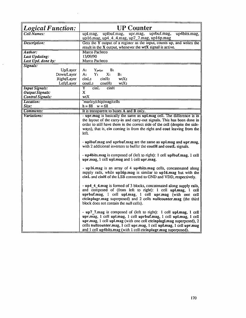
Logical Function: UP CounterC e l l N a m e s : u pl.m ag, uplbuf.m ag, upr.m ag, uprbuf.m ag, up4b its.m ag,
u p l6 .m a g , u p 4_4_4 .m ag , u p 7_7 .m ag , u p l6 p .m a gD e s c r i p t i o n : Gets the Y output o f a register as the input, counts up, and writes the
result in the X output, whenever the wtX signal is active.A u t h o r :
L a s t U p d a t i n g :
L a s t U p d . d o n e b y :
Marco Pacheco 13/09/90 Marco Pacheco
S i g n a l s :Up/Layer
Down/LayerRight/Layer
Left/Layer
Al Ypolyc BlAi Yi Xi Bi cinL2 cinH2 wtX 2
COUtL2 COUtH2 WtX2I n p u t S i g n a l s :
O u t p u t S i g n a l s : C o n t r o l S i g n a l s :
Y cinL cinH XwtX
L o c a t i o n :
S i z e :
Tnarley/chip/mag/cells h = 88 w = 68
C o m m e n t s : It is transparent to buses A and B only.V a r i a t i o n s : - upr.m ag is basically the same as upl.m ag cell. The difference is in
the layout o f the carry-in and carry-out signals. This has been done in order to still have them in the correct side o f the cell (despite the sideways), that is, cin coming in from the right and cout leaving from the left.
- uplbuf.m ag and uprbuf.m ag are the same as upl.m ag and upr.m ag, with 2 additional inverters to buffer the coutH and coutL signals.
- up4bits.m ag is composed o f (left to right): 1 cell uplbuf.m ag, 1 cell upr.m ag, 1 cell upl.m ag and 1 cell upr.m ag.
- up 16.m ag is an array o f 4 up4bits.m ag cells, concatenated along supply rails, while u p l6p .m ag is similar to u p l6 .m a g but with the cinL and cinH o f the LSB connected to GND and V D D, respectively.
- up4_4_4.m ag is formed o f 3 blocks, concatenated along supply rails, and composed o f (from left to right): 1 cell upl.m ag, 1 cell uprbuf.m ag, 1 cell upl.m ag, 1 cell upr.m ag (with one cell ctcinplugr.m ag superposed) and 2 cells nullcounter.m ag (the third block does not contain the null cells).
- up7_7.m ag is composed o f (left to right): 1 cell upl.m ag, 1 cell upr.m ag, 1 cell upl.m ag, 1 cell uprbuf.m ag, 1 cell upl.m ag, 1 cell upr.m ag, 1 cell upl.m ag (with one cell ctcinplugl.m ag superposed), 2 cells nullcounter.m ag, 1 cell upr.m ag, 1 cell upl.m ag, 1 cell upr.m ag and 1 cell up4bits.m ag (with 1 cell ctcinplugr.m ag superposed).
170

Logical Function: Shift left/rightC e l l N a m e s : shift.mag, shiftr.mag, shiftlr.mag, shiftl6.m agD e s c r i p t i o n : Gets the Y output signal of a register and puts either in the X input o f
the register adjacent to the right, if SR is active, or in the X input o f the register adjacent to the left, if SL is active.
A u t h o r :
L a s t U p d a t i n g : L a s t U p d . d o n e b y :
Marco Pacheco 27/06/90 Marco Pacheco
S i g n a l s :
Up/LayerDown/LayerRight/Layer
Left/Layer
Ai Yi Xi Bi Ai Yi Xi Bi SR2 SL2 SR2 SL2
I n p u t S i g n a l s :
O u t p u t S i g n a l s : C o n t r o l S i g n a l s :
YXSR SL
L o c a t i o n :
S i z e :
■"marley/chip/mag/cells h = 22 w = 68
C o m m e n t s : It is transparent to buses A and B only.V a r i a t i o n s : - sh iftl6 .m ag is an array o f 8 shiftlr.m ag cells, concatenated along
supply rails.
Logical Function: 32-bit Shift left/rightC e l l N a m e s : shift2xl6.m ag, ccshiftupl6.m ag, ccshiftdwl6.m agD e s c r i p t i o n : A 32-bit shift register composed o f 2 16-bit shift registers.A u t h o r :
L a s t U p d a t i n g :
L a s t U p d . d o n e b y :
Marco Pacheco 13/09/90 Marco Pacheco
S i g n a l s :
Up/LayerDown/LayerRight/Layer
Left/Layer
Ai Yi Xi Bi Ai Yi Xi Bi SR2 SL2 SR2 SL2
I n p u t S i g n a l s : O u t p u t S i g n a l s :
C o n t r o l S i g n a l s :
YXSR SL
L o c a t i o n :
S i z e :~marley/chip/mag/cells h = see variations w = see variations
C o m m e n t s : - These cells are transparent to buses A and B only.V a r i a t i o n s : - sh ift2x l6 .m ag is the 32-bit shift register, composed o f two separate
16-bit shift registers. It is composed o f (top to bottom): 1 cell ccsh iftupl6 .m ag, 1 cell concat!6 .m ag and 1 cell ccsh iftdw l6.m ag.
- ccsh iftu pl6 .m ag (w = 958, h = 22) is composed o f (left to right): 1 cell sh iftcce.m ag, 1 cell shiftr.m ag, 6 cells shiftlr.m ag, 1 cell shift.m ag and 1 cell shiftzero.m ag. This cell is used as the top 16-bit shift register to form a 32-bit shift register.
- ccsh iftd w l6 .m ag (w = 953, h = 22) is composed o f (left to right): 1 cell shiftself.m ag, 1 cell shiftr.m ag, 6 cells shiftlr.m ag, 1 cell sh ift.m ag and 1 cell shiftccb.m ag. This cell is used as the bottom 16- bit shift register to form a 32-bit shift register.
171

Logical Function: ALUC e l l N a m e s : nalu.mag, nalur.mag, nalubuf.mag, nalu4bits.mag, nalul6.m ag,
nalul6p.magD e s c r i p t i o n : Arithmetic and Logic Unit, controlled by 12 bits: K0-K3 (Kill carry),
P0-P3 (Propagate carry) and R0-R3 (Execution code).A u t h o r :
L a s t U p d a t i n g : L a s t U p d . d o n e b y :
Marco Pacheco 13/09/90 Marco Pacheco
S i g n a l s :
Up/LayerDown/LayerRight/Layer
Left/Layer
Ai alubi aluouti aluai Bi Ai coutHi aluouti aluoutbi Bi K3-K0ndiff P3-P0ndiff CUlLpoly cinHpoly R3-R0ndiff K3-K0ndiff P3-P0ndiff COUtLpoly COUtHpoly R3-R0ndiff
I n p u t S i g n a l s :
O u t p u t S i g n a l s : C o n t r o l S i g n a l s :
cinL cinH alua alub coutL coutH aluout aluoutb K0-K3 P0-P3 R0-R3
L o c a t i o n :
S i z e :“marley/chip/mag/cells h = 452 w = 68
C o m m e n t s : - These cells are transparent to buses A and B only.V a r i a t i o n s : - nalur.m ag is basically the same as nalu.m ag cell. The difference is
in the layout o f the carry-in and carry-out signals. This has been done, in order to still have them in the correct side o f the cell (despite the sideways movement), that is, C IN coming in from the right and COUT leaving from the left.
- nalubuf.m ag is similar to nalu.m ag with 2 additional inverters for cinL and cinH signals, in order to recover the signals to continue the transmission through the cell.
- nalu4bits is composed o f (left to right): 1 cell nalubuf.m ag, 1 cell nalur.m ag, 1 cell nalu.m ag and 1 cell nalur.m ag.
- n alu l6 .m ag is an array o f 4 nalu4bits cells, concatenated along supply rails.
- na lu l6p .m ag is the same as n alu l6 .m ag with the additional plugs - aluplugl.m ag and aluplugr - to transform ndiff and poly layers to metal 1.
172

Logical Function: Bi-directional tri-state bufferC e l l N a m e s : bi3st.mag, bi3stA.mag, bi3stAlr.mag, bi3stA16.mag,
bi3stB.mag, bi3stBlr.mag, bi3stB16.mag, bi3stZ.mag, bi3stZlr.mag, bi3stZ16.mag
D e s c r i p t i o n : Bi-directional tri-state buffer, with different control lines for each direction.
A u t h o r :
L a s t U p d a t i n g :
L a s t U p d . d o n e b y :
Marley Vellasco 13/08/90 Marley Vellasco
S i g n a l s :Up/Layer
Down/LayerRight/Layer
Left/Layer
Ai Yi Xi Zi Bi Ai Yi Xi Zi Bi dpout2 dpoutb2 soloinb2 soloin2 dpout2 dpoutb2 soloinb2 soloin2
I n p u t S i g n a l s :
O u t p u t S i g n a l s : C o n t r o l S i g n a l s :
see comments see commentsdpout dpoutb soloin soloinb
L o c a t i o n :
S i z e :
“marley/chip/mag/cells h = 131 w = 68
C o m m e n t s : - 1'he input and output signals depend on which bus (A , B or Z) is being buffered.
- Each cell is transparent to all buses, except to the one which is being buffered.
V a r i a t i o n s : - bi3st.mag is the basic cell that is used in all variations, namely bi3stA.mag, bi3stB.mag and bi3stZ.mag. This cell does NOT contain any bus.
- bi3st?.mag buffers the bus ? and is transparent to all other buses (where ? can be bus A, B or Z).
- bi3st?lr.mag is composed of two bi3st?.mag cells, which are mirror images of each other.
- bi3st?16.mag is an array of 8 bi3st?lr.mag cells, concatenated along supply rails.
173

Appendix 3
Instruction Control Sequence
This appendix describes the register set and presents the control sequence of the implemented instruction set.
RE GISTERS
REGISTER FUNCTION TYPE #BITS BUS LOC.
AX accumulator 16M PX multiply aux-register mm 16CC condition code register 4 <3:0>ICR instruction code register 4 <15-12>OR operand register 16IP instruction pointer 16X16 multiply loop control 4 <15-12>TC timer count register mm 16M AXC timer maximum count register mm 16NODE node network address mm 16CLUSTER cluster network address mm 16LAYER layer network address mm 16RM righl-channel master input register 16RS right-channel slave input register 16LM left-channel master input register 16LS left-channel slave input register 16RPIB righl-channel pointer to input buffer mm 7 <15-9>LPIB left-channel pointer to input buffer mm 7 <6-0>RSIB right-channel start o f input buffer mm 7 <15-9>LSIB left-channel start o f input buffer mm 7 <6-0>RPOB right-channel pointer to output buffer mm 7 <1S*9>LPOB left-channel pointer to output buffer mm 7 <6-0>RPKT right-channel packets counter mm 7 <15-9>LPKT left-channel packets counter mm 7 <6-0>RSZ right-channel packet size counter mm 4 <9-6>LSZ left-channel packet size counter mm 4 <3-0>PSZ packet size mm 4 ’4’ <9-6;3-0>RNETAD right-channel net. address check 2LNETAD left-channel net. address check 2
CC
bit position 3 2 1 0function = MC OV Z CY
CY CARRYout[15] canyZ !(alu_out[15]+. . . +alu_out[0]) zeroO V CARRYout[15] ©CARRYout[14] overflowMC MPX[-1] multiplier cany
174

CONTROL & IN STRUCTION SEQUENCING
LDAX
O l: AI <bus.A> <— IPA1 <bus.B> <— memA I IFETCH (read mem)AI IC < ~ <bus.B>[15-12]AI OR < - (0000) | <bus.B>[l 1-0]AI decodeIC
0 2 : C2 <bus.A> <— ORC2 <bus.B> <— mem or mmap_regC2 MREADF2C2 AX <— <bus.B>
STAX
O l: A I <bus.A> <— IPA I <bus.B> <-- memA I IC < ~ <bus.B>[15-12)A I IFETCH (read mem)A I OR < - (0000) | <bus.B>[l 1-0]A I decodeIC
0 2 : D2 <bus.A> <— ORD2 <bus.B> <-- AXD2 MWRTTED 2 mem or mmap_reg <-- <bus.B>
ADD
A I <bus.A> < — IPA I <bus.B> <— memA I IC < ~ <bus.B>[15-12]A I OR < ~ (0000) | <bus.B>[l 1-0]A I IFETCH (read mem)A I decodeIC
E2 <bus.A> < — ORE2 <bus.B> <— mem or mmap_regE2 MREADF2E2 ALU_InB < — <bus.B>E2 ALU_InA < - AXE2 AX <— <bus.ALU.out> <— A + B
175

SUB
O l: AI <bus.A> <— IPAI <bus.B> <— memA I I C < - <bus.B>[15-12]AI IFETCH (read mem)AI OR < ~ (0000) | <bus.B>[l 1-0]A I decodeIC
0 2 : E2 <bus.A> <-- ORE2 <bus.B> <— mem or mmap_regE2 MREADF2E2 ALU_InB < - <bus.B>E2 ALU_InA < - AXE2 AX <-- <bus.ALU.out> <-- A - B
AND
O l: AI <bus.A> <— IPA I <bus.B> <-- memA I IFETCH (read mem)A I IC < ~ <bus.B>[15-12]A I OR < - (0000) | <bus.B>[l 1-0]AI decodeIC
0 2 : E2 <bus.A> <— ORE2 <bus.B> <— mem or mmap_regE2 MREADF2E2 ALU_InB <— <bus.B>E2 ALU_InA < - AXE2 AX <— <bus.ALU.out> <-- A a B
OR
O l: A I <bus.A> <— IPA I <bus.B> <— memA I IFETCH (read mem)A I IC <-- <bus.B>[15-12]A I OR <-- (0000) | <bus.B>[l 1-0]A I decodeIC
0 2 : E2 <bus.A> <— ORE2 <bus.B> <— mem or mmap_regE2 MREADF2E2 ALU_InB < — <bus.B>E2 ALU_InA <-- AXE2 AX <— <bus.ALU.oui> <— A v B
176
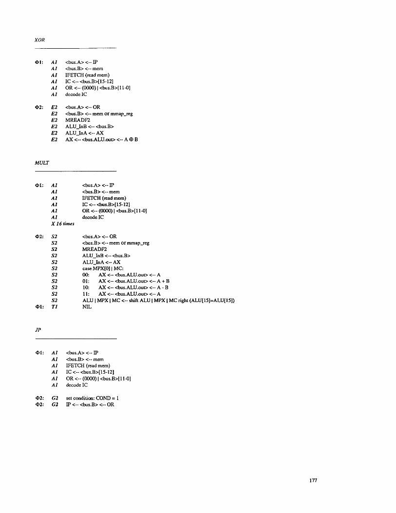
XOR
A I <bus.A> <— IPA I <bus.B> <— memA I IFETCH (read mem)A I IC < ~ <bus.B>[15-12]A I OR < - (0000) | <bus.B>[l 1-0]A I decodeIC
E2 <bus.A> <— ORE2 <bus.B> <— mem or mmap_regE2 MREADF2E2 ALU_InB <-- <bus.B>E2 ALU_InA < - AXE2 AX < — <bus.ALU.out> <— A © B
MULT
A I <bus.A> <— IPA I <bus.B> <-- memA I IFETCH (read mem)A I IC < ~ <bus.B>[15-12]A I OR < ~ (0000) | <bus.B>[l 1-0]A I decodeICX 16 times
S2 <bus.A> <-- ORS2 <bus.B> <— mem or mmap_regS2 MREADF2S2 ALU_InB <— <bus.B>S2 A L U JnA < - AXS2 case MPX[0] | MC:S2 00: AX <-- <bus.ALU.out> <— AS2 01: AX < --<bus.ALU.out> < --A + BS2 10: AX <-- <bus.ALU.out> <-- A - BS2 11: AX <-- <bus. ALU.out> <— AS2 ALU | MPX | MC < » shift ALU | MPX | MC right (ALU[15]T1 NIL
JP
<&1: A I <bus.A> <-- IPA I <bus.B> <— memA I IFETCH (read mem)A I IC < ~ <bus.B>[15-12]A I OR < - (0000) | <bus.B>[l 1-0]A I decodeIC
0 2 : G2 set condition: COND = 10 2 : G2 IP <— <bus.B> <— OR
177
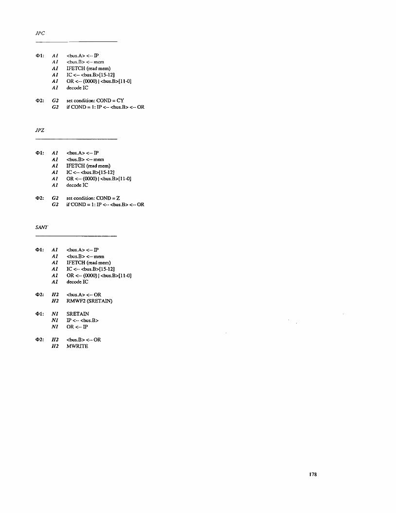
JPC
<t>l: A I <bus.A ><—IPA I <bus.B> <—memA I IFETCH (read mem)A I IC < — <bus.B>[15-12]A I OR <-- (0000) | <bus.B>[l 1-0]A 1 decodeIC
<t>2: G2 set condition: COND = CYG2 if COND = 1: IP < ~ <bus.B> < - OR
JPZ
<D1: A I <bus.A> <— IPA I <bus.B> <-- memA I IFETCH (read mem)A I IC < ~ <bus.B>[15-12]A I OR < - (0000) | <bus.B>[l 1-0]A I decodeIC
<S>2: G2 set condition: COND = ZG2 if COND = I : IP <-- <bus.B> < - OR
SANT
<D1: A I <bus.A> <-- IPA I <bus.B> <-- memA I IFETCH (read mem)A I IC <— <bus.B>[15-12]A I OR < - (0000) | <bus.B>[l 1-0]A I decode IC
0 2 : 112 <bus.A> <— ORH 2 RMWF2 (SRETAIN)
«M: N1 SRETALNN1 IP < — <bus.B>N1 OR < - IP
<D2: 112 <bus.B> <-- OR112 MWRTTE
178

STfN
O l: A I <bus.A> < — IPA I <bus.B> <— meinA I IFETCH (read mem)A I IC < ~ <bus.B>[15-12]A I OR < - (0000) | <bus.B>[l 1-01A I decode IC
0 2 : B2 <bus.A> <-- ORB2 <bus.B> <— mem or mmap_regB2 MREADF2B2 OR <-- <bus.B>
O l: S I NIL
0 2 : D2 <bus.A> <— OR ; enable.mopD2 <bus.B> <-- AXD2 mem or mmap_ieg <— <bus.B>D2 MWRITE
LDI
O l: A I <bus.A> <-- IPA I <bus.B> <— memA I IFETCH (read mem)A I IC < - <bus.B>[15-12]A I OR < - (0000) | <bus.B >[ll-0]A I decodeIC
0 2 : 12 AX <-- <bus.B> <— OR
GET
O l: A I <bus.A> <-- IPA I <bus.B> <— memA I IFETCH (read mem)A I IC < ~ <bus.B>[15-12]A I OR < - (0000) | <bus.B>[l 1-0]
0 2 : X2 <bus.A> <-- ORX2 <bus.B> <-- mem or mmap_regX2 MREADF2X2 ALU_InB <— <bus.B>X2 ALU_InA < - AXX2 AX <-- <bus.ALU.out> <— A +
O l: N1 NIL
0 2 : K2 <bus.A> <— AXK2 <bus.B> <-- mem or mmap regK2 MREADF2K2 AX <— <bus.B>
179

MAP
O l: A I <bus.A> <— IPA I <bus.B> <-- memA I IFETCH (read mem)A I IC < ~ <bus.B>[15-12]A I OR < - (0000) | <bus.B>[l 1-0]A I decodeIC
0 2 : Y2 <bus.A> <— ORY2 enable mmap_operations
INTERRUPT
O l: 0 1 <bus.A> <— INTVECTO l disable interrupt 0 1 IP < — <bus.B>O l RMWF1 (SRETAIN) O l OR < — IP
0 2 : P2 <bus.B> <— ORP2 MWRTTE
180
Appendix 4
Microprocessor Schematic Diagrams
This appendix presents sample diagrams of the prototype Neural-RISC chip.
181

« 5 «sz 5o £ ^ o 51 i£h'
C \ = ^tr / V vh-a /L _A ts
V"a <ii “ft
-t
f\ A /va (/ i/ ir if irh i- i-c_cr <_rs Ci t;fS- - VV V
< a;
Cl Z Z €X A A A•a 5 £ £• *> 5> h S 3 ^ ^ i;
n o n •2-? ?fc! £ £ £ 5
Ar r If<a
<a c cc? fS
- <vIrrHc V
rj . j. _a a ft
2«-H5a
a&i_fi! _fi]
\ £ \ H
hr ¥—1>
> ! > ; > i frali d
> >lO Q in c s i n
A A AL - if if ifu ( fH-( MUH S <SG(.. VV V
a ft 4 ■ftCN<c<a
N 2 Z <N A A A !& «» ,“■£} «; £
l Ssl|!S<E 0*1
. « Q Q CMA ^5 < O Q A A
i i 3 f- J “-p . 3 j I vf2j2fti = clee; S £ £ 5 3 3
c<
J 12-<CM
«l2 T T
Pro
cess
or
Neu
rol-
RIS
C
Chi
p

»2-
i $
■«- X c .= *. =: v. t= 1±a ™
c s - c
1/ #- ;= L- L- Ll Ll
2 22 - -a -
c-cS'C S' ‘- i- ir u" a"
cjatk. a “
£ Tf, ^ 5- w m m m 2 2 a. a. a. JX O- O- .n -o .cSJSQca:JpiOOouooSQtQ. f a J p J r i M U H H U U O O SI A A A A A A
i i3 g d o j 2 e t £ g g S § 3 S 3 S i ' S S 5 i 5~ S i S ^ K ^ W W M W V V V V V VC j C P o U h ^ ^ t - Q O i t l l O Q 0 o- »- »3?zo«a: o: J—’ * ~Q U U U K 6 K J C Ja 5 a: -»
fiSficgfldf ’ K y J X I I J J U U U O : . . _ __ _2 2 2 a ; D . a . Q . f i . o o i / > v i ( i ) i r j a : i i : a ; a :gSi i g*
" A /y
5 ? ! ?3 5 5 ?
OFu.Q=Q:i -cr» = Ses^;C2
-S'41 2cz-
t i - a - a
H2: (7 :
c ^ V z'
; e t = ^ s s l :lc-d.cSt a $
^ ^ U. & a ? -c 3 ■= lj- c | c * c — = Ll Ll Ll Ll
u i I 2 2 3 23cdScdQ; —j
i n '■ o ^ K E U u ,
■Sf35lES*s iS ■ i S - S K
“ AAA2 ut id tn i o *- *- - <& a £ V V V
» Q• < Q Q « ' I ? ? ffl I o o a a
B s s s i i . » h H i U i U m* j5«^oSaddo£ o 5 S *a : ( i . a Q . £ £ Q : j u & u t o o a : j £ £ i e j i i : j
£ ££ 5 g o o gj j t
V vca
A A A A A
< V o. V V
O <N O <N C.C ^ :<-C ca
c .c . ' ccCCE_
1 <i (ocu u u u LlaL~2 3 2 3 25§ a a . - C2
A A (2) A Cl U Clz£
Q. 2ao<a.
o<Q.
o<a Q.
<Ea: oOAO(C w
a:gra
Ia.ja
8<ACC
o
Neu
ral-
RIS
C
Mic
ropr
oces
sor
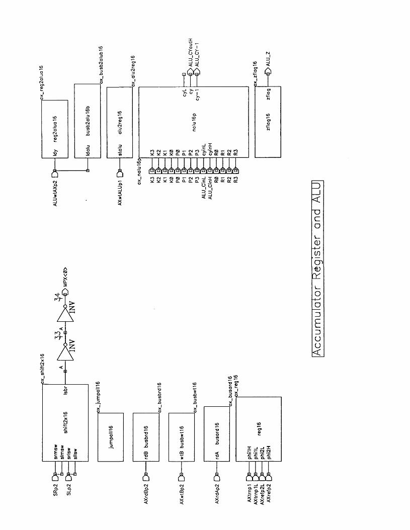
o o
n < N ' - Q S ' - M l O - I I S ^ ^ ^ y q . Q - q . 0 . c C a:
11< <X
a o Z? >* ^ 9
CMa .
CMCL
- JCO
1Xo
1K3
1X3
t oCO (D t£>
*oT>
o V_ * oQ_ . O . a£ CO
3CO3
3n3 -O .O
CD CO <T? ■o
A A A
»— — CM <N
A WCL «- CM Q.
Acc
umul
ator
R
egis
ter
and
ALU

s £ 115 d 5 £ B £9*gg
B £IsfiSS
5
cocoa
Inte
rrupt
C
ontro
ller

J * l l fiH j I I i^ « w » . « r -M » 4 « R i I I H M H * - I j I I m *a tmm I I L . i im f L r J F l I I I I P * : j -■» I ! w a r< £ - - £ * 1 I I
l i s r ^ j l ic u ^ l l IISSS3II£££511i i s a f l i i i c s i i i i s a i i i i r s ni j iT ikBi i a u n i i j i i m i A i i r w ^ ii
HZllMUKJll ; S 3 I I K i a i l l K ! : . S 3 I11* • *» i«;-i | | ■* -* * 1 | | "■•**> i i I * * »i |I I I i* .-J I I L.. 4 4 I ] I I I I £ „ ..J I I Im m . h -* I I Il i ; : s = 3 i l C = j : ; i l l i ; : : r 3 M t = : : ; i li i : n » n i c : i : i i i i : j : » i i i « : : i : i ii ■< s J ■ $ ! 11 t f a - s !■ 11 * s 1 1 k * l a )■ i
S 3 I I E S :? I
a i i i t t r : z i i
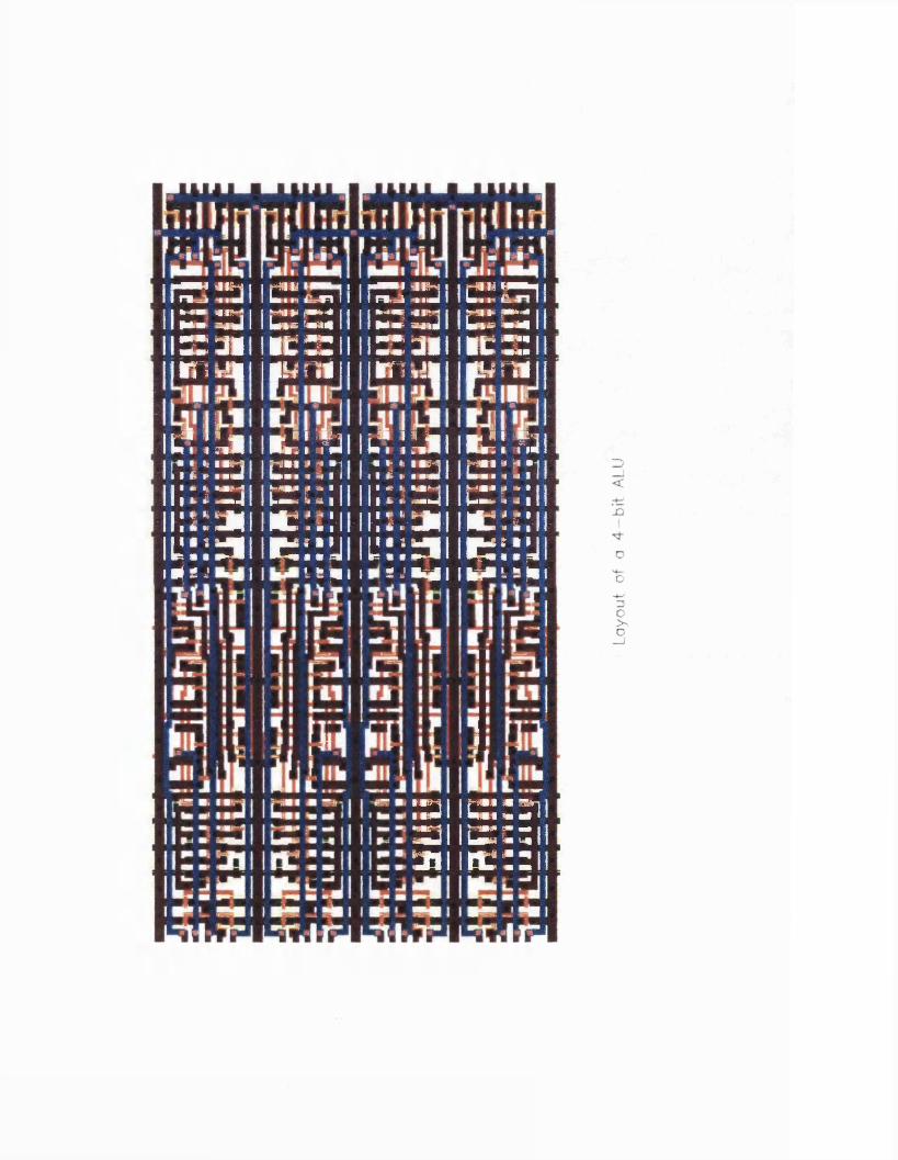
j « il tb i | | H l f l « | M *S H i i j H M i M " « -l II I r» ! I Ut.i fLrlFl I I I I r»ru i '■ awJ I ! Iwi 11 & I I
lit*: z j \ i c r c s i i i i s z s a i i g t k i ii i s a i n i c s i i i i s a i i i i c r : ! !M n ^ t H i i a u n a i i i i m * j a i i a u ; a n
It* : t a i l it ! ! t i \ It” \IM\ l it ! ! S3!I r * * »? I W r 'l I I M M * r* * i I I -■ »- is 1 m * + I I M M * r< » i II I I 6 f i»J I I L.. ,-,1(1 [ i I & * ..J I I Im m . n * I I Ii i ; : 3 Z 3 M C = e : ; i i i i ; : i = 3 M C = : : ; i i i i i f J i M t : . : i i i i : : : j n i t ^ : : n i u : j a i i r ; ! : ! j i i L ! : . j a i i i R ; : : y i• M * J I I l i p i i * •' >ifl I I l i* t * (■ I
; s i i t s : n is i i s c z i ia iiit tr :z n