a novel 8t cell-based subthreshold static ram for ultra
TRANSCRIPT
electronics
Article
A Novel 8T Cell-Based Subthreshold Static RAM forUltra-Low Power Platform Applications
Taehoon Kim, Sivasundar Manisankar and Yeonbae Chung *
School of Electronics Engineering, Kyungpook National University, Daegu 41566, Korea;[email protected] (T.K.); [email protected] (S.M.)* Correspondence: [email protected]; Tel.: +82-53-950-5522
Received: 22 January 2020; Accepted: 28 May 2020; Published: 2 June 2020�����������������
Abstract: Subthreshold SRAMs profit various energy-constrained applications. The traditional 6TSRAMs exhibit poor cell stability with voltage scaling. To this end, several 8T to 16T cell designshave been reported to improve the stability. However, they either suffer one of disturbances orconsume large bit-area overhead. Furthermore, some cell options have a limited write-ability.This paper presents a novel 8T static RAM for reliable subthreshold operation. The cell employs afully differential scheme and features cross-point access. An adaptive cell bias for each operatingmode eliminates the read disturbance and enlarges the write-ability as well as the half-select stabilityin a cost-effective small bit-area. The bit-cell also can support efficient bit-interleaving. To verify theSRAM technique, a 32-kbit macro incorporating the proposed cell was implemented with an industrial180 nm low-power CMOS process. At 0.4 V and room temperature, the proposed cell achieves3.6× better write-ability and 2.6× higher dummy-read stability compared with the commercialized8T cell. The 32-kbit SRAM successfully operates down to 0.21 V (~0.27 V lower than transistorthreshold voltage). At its lowest operating voltage, the sleep-mode leakage power of entire SRAMis 7.75 nW. Many design results indicate that the proposed SRAM design, which is applicable toan aggressively-scaled process, might be quite useful in realizing cost-effective robust ultra-lowvoltage SRAMs.
Keywords: subthreshold SRAM; ultra-low power; cell stability; 8T cell
1. Introduction
Embedded SRAMs are a critical component in memory rich network-on-chip or SoC designs.They are used as buffer memories or caches, and occupy a large portion of area in current system VLSIs.Especially in energy-constrained low-speed biomedical devices and other emerging applications likewireless sensor networks and many wearable devices, subthreshold SRAM designs to extend systemoperating life-time from limited energy resource have become an ever-important issue. Loweringsupply voltage (VDD) down to transistor threshold-voltage (VTH) level decreases CMOS switchingpower quadratically and decreases first-order leakage power linearly [1]. However, reliable circuitdesign for proper subthreshold operation is extremely challenging because of reduced design marginsand increased device variations.
The widely adopted conventional 6T SRAMs exhibit poor cell stability with VDD scaling,thus severely limiting the minimum operating voltage (VMIN). To cope with the stability problem atdeep-low voltage regime, various SRAM cells composed of different number of transistors have beenexplored. The common approach utilizes a dedicated read port to separate the data storage nodesfrom the read path, thereby eliminating the read disturbance [2–10]. However, these read-decoupled(RD) cells suffer the half-select disturbance while writing into a cell, hence they cannot support anefficient bit-interleaving structure. Some 8T, 9T, 10T, and 12T SRAM cells [11–16] employ cross-point
Electronics 2020, 9, 928; doi:10.3390/electronics9060928 www.mdpi.com/journal/electronics
Electronics 2020, 9, 928 2 of 17
(CP) access to eliminate the half-select disturbance. However, the CP cell options composed of eighttransistors [11,12] eliminate the half-select disturbance only. They still suffer the read disturbance.Moreover, the CP 8T cell in [11] has a limited write capability owing to its serial access transistors. OtherCP cell options composed of 9, 10, and 12 transistors [13–16] eliminate the read disturbance as wellas the half-select disturbance. However, cross-point cells in [13–15] consume large bit-area overhead.Furthermore, CP cells in [13,14,16] have a limited write capability owing to their serial access transistors.The other approaches (Schmitt-trigger-based 10T cell [17], P-P-N-based 10T cell [18], and 1-read/1-write16T cell [19]) may achieve a good read stability and can provide an efficient bit-interleaving in column.However, the bit-cell area overhead of those is as high as 110% [17,18] and 800% [19] compared withthe traditional 6T cell.
Besides the cell stability issue, reducing the bitline switching power is also important to achieve lowpower SRAM. The memory bitlines usually have a heavy capacitive loading. Whenever write or readoperation is performed, switching the heavy bitlines costs significant power dissipation. In this paper,we present a novel 8T cell based static RAM for robust subthreshold operation. Our previous work [20]conceptualized the bit-cell operation roughly without detailed core and peripheral circuits. This work,which extends that of [20], seeks the bit performance and all (read, write, row half-select, and columnhalf-select) stability metrics of our proposed cell in greater detail, and verifies the subthreshold SRAMtechniques in a 32-kbit prototype designed with an industrial CMOS process technology. This SRAMdesign extremely reduces the bitline switching power of non-selected columns, and successfullyoperates down to deep-low supply voltage.
2. Proposed 8T SRAM Cell
2.1. Bit-Cell Structure and Layout
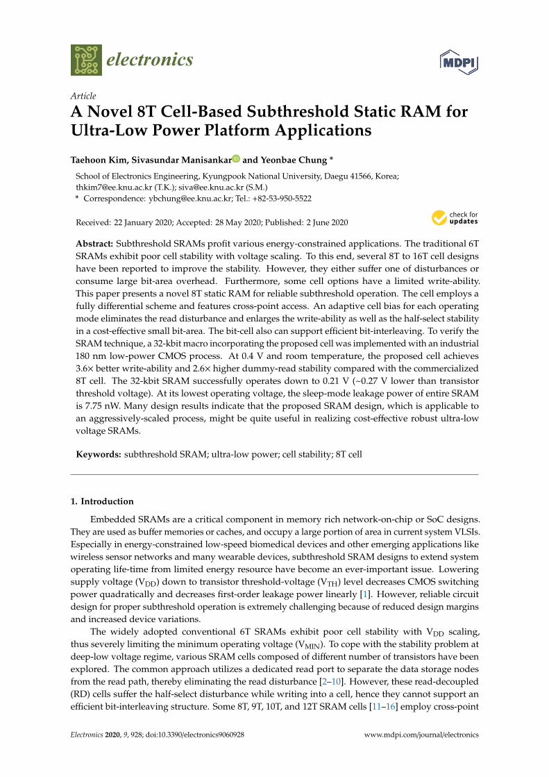
Figure 1 depicts the configuration of the proposed cell, along with the commercialized RD-8Tcell [2] for comparison. The proposed 8T cell consists of two load transistors (P1, P2), two drivetransistors (N1, N2), two access transistors (N3, N4), and two conducting transistors (P3, P4) betweenthe access device and the drive device. The wordline (WL) is row-based, and the bitline (BL), /bitline(/BL), and column-wise assistline (CAL) are column-based. It has a fully differential symmetricconfiguration, and utilizes relatively simple one-row/three-column control lines. Table 1 lists the biasconditions of the proposed cell for each operating mode.
Electronics 2020, 9, x FOR PEER REVIEW 2 of 16
transistors [11,12] eliminate the half-select disturbance only. They still suffer the read disturbance. Moreover, the CP 8T cell in [11] has a limited write capability owing to its serial access transistors. Other CP cell options composed of 9, 10, and 12 transistors [13–16] eliminate the read disturbance as well as the half-select disturbance. However, cross-point cells in [13–15] consume large bit-area overhead. Furthermore, CP cells in [13,14,16] have a limited write capability owing to their serial access transistors. The other approaches (Schmitt-trigger-based 10T cell [17], P-P-N-based 10T cell [18], and 1-read/1-write 16T cell [19]) may achieve a good read stability and can provide an efficient bit-interleaving in column. However, the bit-cell area overhead of those is as high as 110% [17,18] and 800% [19] compared with the traditional 6T cell.
Besides the cell stability issue, reducing the bitline switching power is also important to achieve low power SRAM. The memory bitlines usually have a heavy capacitive loading. Whenever write or read operation is performed, switching the heavy bitlines costs significant power dissipation. In this paper, we present a novel 8T cell based static RAM for robust subthreshold operation. Our previous work [20] conceptualized the bit-cell operation roughly without detailed core and peripheral circuits. This work, which extends that of [20], seeks the bit performance and all (read, write, row half-select, and column half-select) stability metrics of our proposed cell in greater detail, and verifies the subthreshold SRAM techniques in a 32-kbit prototype designed with an industrial CMOS process technology. This SRAM design extremely reduces the bitline switching power of non-selected columns, and successfully operates down to deep-low supply voltage.
2. Proposed 8T SRAM Cell
2.1. Bit-Cell Structure and Layout
Figure 1 depicts the configuration of the proposed cell, along with the commercialized RD-8T cell [2] for comparison. The proposed 8T cell consists of two load transistors (P1, P2), two drive transistors (N1, N2), two access transistors (N3, N4), and two conducting transistors (P3, P4) between the access device and the drive device. The wordline (WL) is row-based, and the bitline (BL), /bitline (/BL), and column-wise assistline (CAL) are column-based. It has a fully differential symmetric configuration, and utilizes relatively simple one-row/three-column control lines. Table 1 lists the bias conditions of the proposed cell for each operating mode.
(a) (b)
Figure 1. SRAM cell schematics: (a) proposed 8T cell; (b) RD-8T cell [2]. WL, wordline; BL, bitline; CAL, column-wise assistline; DN, data-node.
Table 1. Operational conditions of the proposed 8T SRAM cell. WL, wordline; BL, bitline; CAL, column-wise assistline.
WL BL /BL CAL Standby 0 VDD VDD 0
Read VPP 0 (floating) 0 (floating) VDD Write VPP VDD / 0 0 / VDD NVGG
VPP = ~1.3VDD, NVGG = −0.85VDD.
/PNPN
DN/DN
N1 N2
P2
N4
BL /BL
WL
P3
CAL
P4
P1
N3
DN /DN
P1
N1
N3
N2
P2
N4
WBL /WBL
WWL
RWL
N6
N5
RBL
Figure 1. SRAM cell schematics: (a) proposed 8T cell; (b) RD-8T cell [2]. WL, wordline; BL, bitline;CAL, column-wise assistline; DN, data-node.
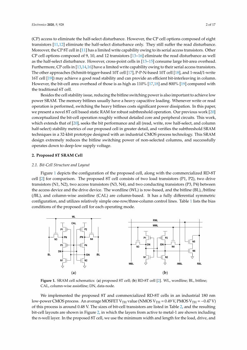
We implemented the proposed 8T and commercialized RD-8T cells in an industrial 180 nmlow-power CMOS process. An average MOSFET VTH value (NMOS VTH = 0.49 V, PMOS VTH =−0.47 V)of this process is around 0.48 V. The sizes of bit-cell transistors are listed in Table 2, and the resultingbit-cell layouts are shown in Figure 2, in which the layers from active to metal-1 are shown includingthe n-well layer. In the proposed 8T cell, we use the minimum width and length for the load, drive, and
Electronics 2020, 9, 928 3 of 17
conducting transistors. For the access transistors, we use the minimum length, but a 1.91× enlargedwidth to enhance the cell write-ability. The active, poly, contact, via, and metal are shared as much aspossible to minimize the bit-area. The area of the proposed cell is 2.31 × 4.02 µm2, almost equal to theRD-8T cell.
Table 1. Operational conditions of the proposed 8T SRAM cell. WL, wordline; BL, bitline; CAL,column-wise assistline.
WL BL /BL CAL
Standby 0 VDD VDD 0Read VPP 0 (floating) 0 (floating) VDDWrite VPP VDD/0 0/VDD NVGG
VPP = ~1.3VDD, NVGG = −0.85VDD.
Table 2. Dimension of cell transistors.
Proposed 8T RD-8T
Width/Length(nm/nm)
P1, P2 220/180 220/180N1, N2 220/180 420/180N3, N4 420/180 220/180N5, N6 - 420/180P3, P4 220/180 -
Electronics 2020, 9, x FOR PEER REVIEW 3 of 16
We implemented the proposed 8T and commercialized RD-8T cells in an industrial 180 nm low-power CMOS process. An average MOSFET VTH value (NMOS VTH = 0.49 V, PMOS VTH = −0.47 V) of this process is around 0.48 V. The sizes of bit-cell transistors are listed in Table 2, and the resulting bit-cell layouts are shown in Figure 2, in which the layers from active to metal-1 are shown including the n-well layer. In the proposed 8T cell, we use the minimum width and length for the load, drive, and conducting transistors. For the access transistors, we use the minimum length, but a 1.91× enlarged width to enhance the cell write-ability. The active, poly, contact, via, and metal are shared as much as possible to minimize the bit-area. The area of the proposed cell is 2.31 × 4.02 µm2, almost equal to the RD-8T cell.
Table 2. Dimension of cell transistors.
Proposed 8T RD-8T
Width/Length (nm/nm)
P1, P2 220/180 220/180 N1, N2 220/180 420/180 N3, N4 420/180 220/180 N5, N6 - 420/180 P3, P4 220/180 -
(a) (b)
Figure 2. Bit-cell layouts: (a) proposed 8T; (b) RD-8T.
2.2. Standby Mode
The proposed 8T cell employs cross-point access. During the standby, BL and /BL are precharged to VDD, WL is forced to ground, and the column-based CAL is forced to ground. This turns on the conducting transistors (P3, P4), thus the cross-coupled latch (P1-N1, P2-N2) with on-state conducting transistors holds bi-stable data. For example, if the data-node (DN) stores a low-state, the /data-node (/DN) maintains VDD because the conducting transistor P4 can pass a strong high-state. If /DN is low, on the other hand, DN maintains a high-state through the conducting transistor P3. Therefore, a sufficient stability can be achieved in the standby mode.
2.3. Read Operation
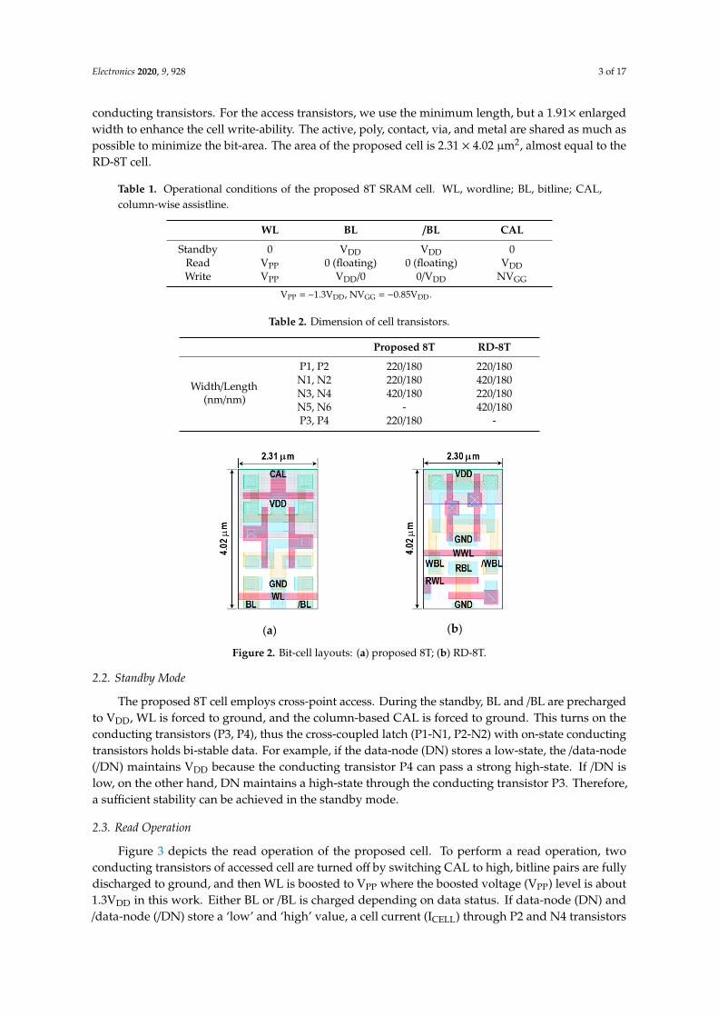
Figure 3 depicts the read operation of the proposed cell. To perform a read operation, two conducting transistors of accessed cell are turned off by switching CAL to high, bitline pairs are fully discharged to ground, and then WL is boosted to VPP where the boosted voltage (VPP) level is about 1.3VDD in this work. Either BL or /BL is charged depending on data status. If data-node (DN) and /data-node (/DN) store a ‘low’ and ‘high’ value, a cell current (ICELL) through P2 and N4 transistors will flow to /BL. This raises the /BL voltage level, which can be compared with the pre-discharged BL value. If DN and /DN store a ‘high’ and ‘low’ value, then the load transistor P1 conducts. Thus, ICELL will flow to BL, raising the BL level, which can be compared with the discharged /BL. As the conducting transistors are turned off during the read access, there is no direct disturbance on true
Figure 2. Bit-cell layouts: (a) proposed 8T; (b) RD-8T.
2.2. Standby Mode
The proposed 8T cell employs cross-point access. During the standby, BL and /BL are prechargedto VDD, WL is forced to ground, and the column-based CAL is forced to ground. This turns on theconducting transistors (P3, P4), thus the cross-coupled latch (P1-N1, P2-N2) with on-state conductingtransistors holds bi-stable data. For example, if the data-node (DN) stores a low-state, the /data-node(/DN) maintains VDD because the conducting transistor P4 can pass a strong high-state. If /DN islow, on the other hand, DN maintains a high-state through the conducting transistor P3. Therefore,a sufficient stability can be achieved in the standby mode.
2.3. Read Operation
Figure 3 depicts the read operation of the proposed cell. To perform a read operation, twoconducting transistors of accessed cell are turned off by switching CAL to high, bitline pairs are fullydischarged to ground, and then WL is boosted to VPP where the boosted voltage (VPP) level is about1.3VDD in this work. Either BL or /BL is charged depending on data status. If data-node (DN) and/data-node (/DN) store a ‘low’ and ‘high’ value, a cell current (ICELL) through P2 and N4 transistors
Electronics 2020, 9, 928 4 of 17
will flow to /BL. This raises the /BL voltage level, which can be compared with the pre-dischargedBL value. If DN and /DN store a ‘high’ and ‘low’ value, then the load transistor P1 conducts. Thus,ICELL will flow to BL, raising the BL level, which can be compared with the discharged /BL. As theconducting transistors are turned off during the read access, there is no direct disturbance on truestorage nodes of our cell. The data-nodes are decoupled from the read path. This read mechanism,which is similar to the RD-8T cell, prevents disturbing the internal stored data. After reading the cell,WL and CAL return to ground in sequence, inducing the cross-coupled latch (P1-N1, P2-N2) withon-state conducting transistors to restore bi-stable data.
Electronics 2020, 9, x FOR PEER REVIEW 4 of 16
storage nodes of our cell. The data-nodes are decoupled from the read path. This read mechanism, which is similar to the RD-8T cell, prevents disturbing the internal stored data. After reading the cell, WL and CAL return to ground in sequence, inducing the cross-coupled latch (P1-N1, P2-N2) with on-state conducting transistors to restore bi-stable data.
Figure 3. Read operation of the proposed 8T cell.
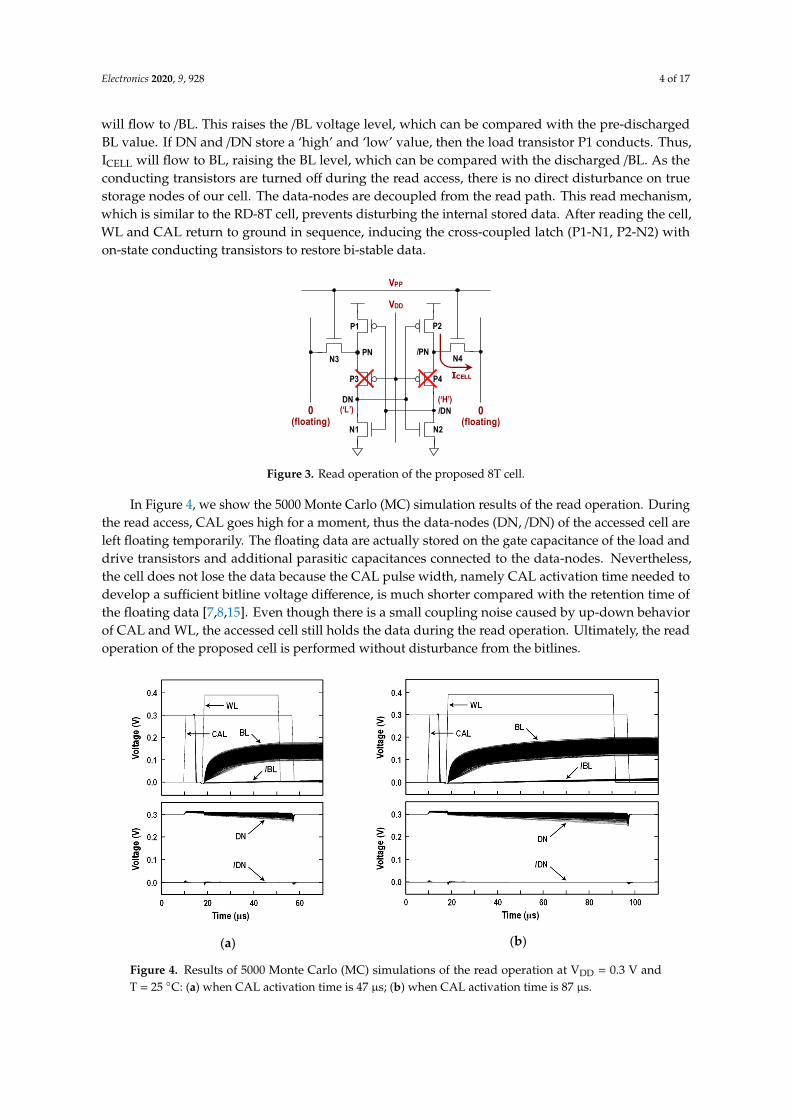
In Figure 4, we show the 5000 Monte Carlo (MC) simulation results of the read operation. During the read access, CAL goes high for a moment, thus the data-nodes (DN, /DN) of the accessed cell are left floating temporarily. The floating data are actually stored on the gate capacitance of the load and drive transistors and additional parasitic capacitances connected to the data-nodes. Nevertheless, the cell does not lose the data because the CAL pulse width, namely CAL activation time needed to develop a sufficient bitline voltage difference, is much shorter compared with the retention time of the floating data [7,8,15]. Even though there is a small coupling noise caused by up-down behavior of CAL and WL, the accessed cell still holds the data during the read operation. Ultimately, the read operation of the proposed cell is performed without disturbance from the bitlines.
(a) (b)
Figure 4. Results of 5000 Monte Carlo (MC) simulations of the read operation at VDD = 0.3 V and T = 25 °C: (a) when CAL activation time is 47 µs; (b) when CAL activation time is 87 µs.
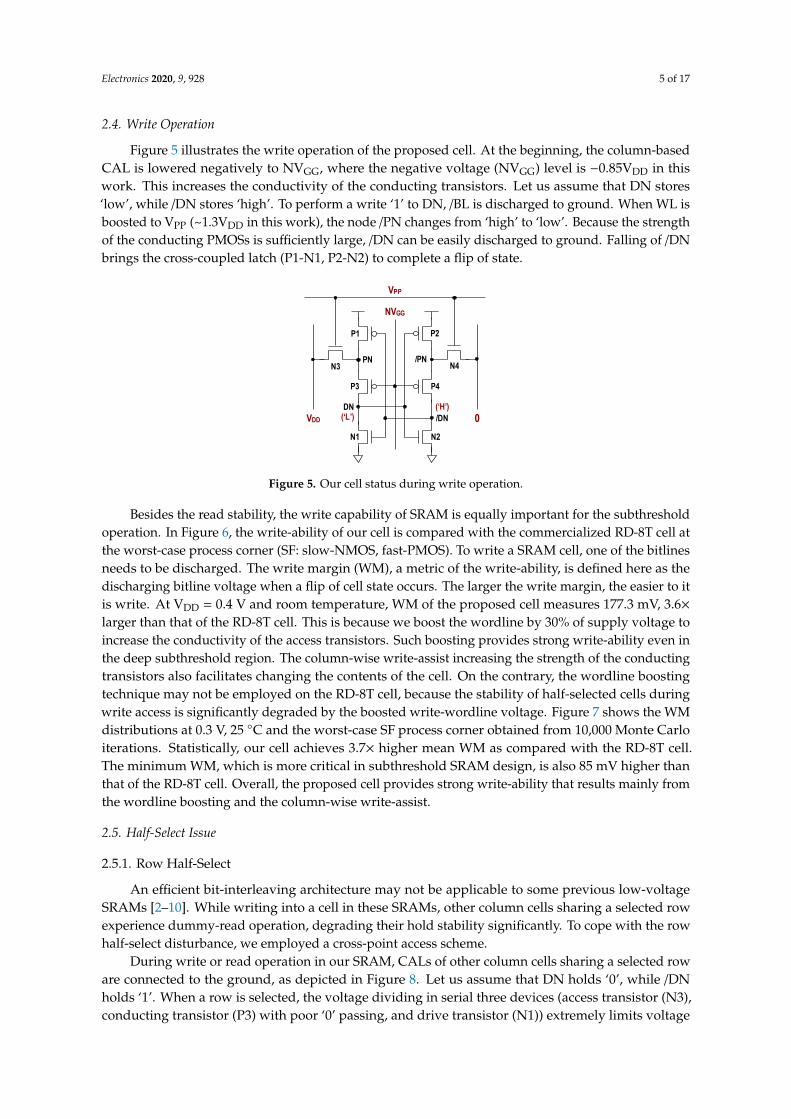
2.4. Write Operation
Figure 5 illustrates the write operation of the proposed cell. At the beginning, the column-based CAL is lowered negatively to NVGG, where the negative voltage (NVGG) level is −0.85VDD in this work. This increases the conductivity of the conducting transistors. Let us assume that DN stores ’low’, while /DN stores ’high’. To perform a write ‘1’ to DN, /BL is discharged to ground. When WL is boosted to VPP (~1.3VDD in this work), the node /PN changes from ‘high’ to ‘low’. Because the strength
PN /PN
/DNDN
N1 N2
P2
N4
P3
VDD
P4 ICELL
(‘L’)(‘H’)
P1
N3
0(floating)
0(floating)
VPP
Figure 3. Read operation of the proposed 8T cell.
In Figure 4, we show the 5000 Monte Carlo (MC) simulation results of the read operation. Duringthe read access, CAL goes high for a moment, thus the data-nodes (DN, /DN) of the accessed cell areleft floating temporarily. The floating data are actually stored on the gate capacitance of the load anddrive transistors and additional parasitic capacitances connected to the data-nodes. Nevertheless,the cell does not lose the data because the CAL pulse width, namely CAL activation time needed todevelop a sufficient bitline voltage difference, is much shorter compared with the retention time ofthe floating data [7,8,15]. Even though there is a small coupling noise caused by up-down behaviorof CAL and WL, the accessed cell still holds the data during the read operation. Ultimately, the readoperation of the proposed cell is performed without disturbance from the bitlines.
Electronics 2020, 9, x FOR PEER REVIEW 4 of 16
storage nodes of our cell. The data-nodes are decoupled from the read path. This read mechanism, which is similar to the RD-8T cell, prevents disturbing the internal stored data. After reading the cell, WL and CAL return to ground in sequence, inducing the cross-coupled latch (P1-N1, P2-N2) with on-state conducting transistors to restore bi-stable data.
Figure 3. Read operation of the proposed 8T cell.
In Figure 4, we show the 5000 Monte Carlo (MC) simulation results of the read operation. During the read access, CAL goes high for a moment, thus the data-nodes (DN, /DN) of the accessed cell are left floating temporarily. The floating data are actually stored on the gate capacitance of the load and drive transistors and additional parasitic capacitances connected to the data-nodes. Nevertheless, the cell does not lose the data because the CAL pulse width, namely CAL activation time needed to develop a sufficient bitline voltage difference, is much shorter compared with the retention time of the floating data [7,8,15]. Even though there is a small coupling noise caused by up-down behavior of CAL and WL, the accessed cell still holds the data during the read operation. Ultimately, the read operation of the proposed cell is performed without disturbance from the bitlines.
(a) (b)
Figure 4. Results of 5000 Monte Carlo (MC) simulations of the read operation at VDD = 0.3 V and T = 25 °C: (a) when CAL activation time is 47 µs; (b) when CAL activation time is 87 µs.
2.4. Write Operation
Figure 5 illustrates the write operation of the proposed cell. At the beginning, the column-based CAL is lowered negatively to NVGG, where the negative voltage (NVGG) level is −0.85VDD in this work. This increases the conductivity of the conducting transistors. Let us assume that DN stores ’low’, while /DN stores ’high’. To perform a write ‘1’ to DN, /BL is discharged to ground. When WL is boosted to VPP (~1.3VDD in this work), the node /PN changes from ‘high’ to ‘low’. Because the strength
PN /PN
/DNDN
N1 N2
P2
N4
P3
VDD
P4 ICELL
(‘L’)(‘H’)
P1
N3
0(floating)
0(floating)
VPP
Figure 4. Results of 5000 Monte Carlo (MC) simulations of the read operation at VDD = 0.3 V andT = 25 ◦C: (a) when CAL activation time is 47 µs; (b) when CAL activation time is 87 µs.
Electronics 2020, 9, 928 5 of 17
2.4. Write Operation
Figure 5 illustrates the write operation of the proposed cell. At the beginning, the column-basedCAL is lowered negatively to NVGG, where the negative voltage (NVGG) level is −0.85VDD in thiswork. This increases the conductivity of the conducting transistors. Let us assume that DN stores‘low’, while /DN stores ‘high’. To perform a write ‘1’ to DN, /BL is discharged to ground. When WL isboosted to VPP (~1.3VDD in this work), the node /PN changes from ‘high’ to ‘low’. Because the strengthof the conducting PMOSs is sufficiently large, /DN can be easily discharged to ground. Falling of /DNbrings the cross-coupled latch (P1-N1, P2-N2) to complete a flip of state.
Electronics 2020, 9, x FOR PEER REVIEW 5 of 16
of the conducting PMOSs is sufficiently large, /DN can be easily discharged to ground. Falling of /DN brings the cross-coupled latch (P1-N1, P2-N2) to complete a flip of state.
Figure 5. Our cell status during write operation.
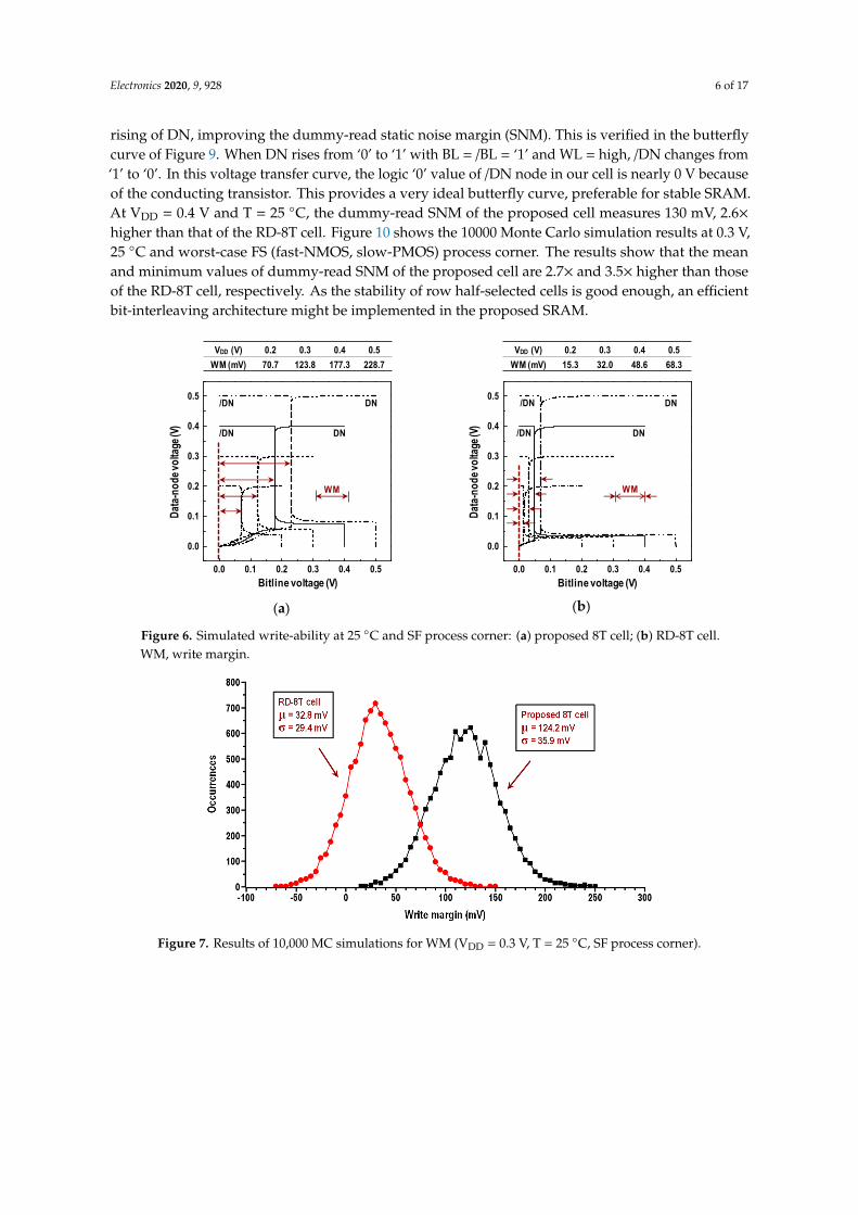
Besides the read stability, the write capability of SRAM is equally important for the subthreshold operation. In Figure 6, the write-ability of our cell is compared with the commercialized RD-8T cell at the worst-case process corner (SF: slow-NMOS, fast-PMOS). To write a SRAM cell, one of the bitlines needs to be discharged. The write margin (WM), a metric of the write-ability, is defined here as the discharging bitline voltage when a flip of cell state occurs. The larger the write margin, the easier to it is write. At VDD = 0.4 V and room temperature, WM of the proposed cell measures 177.3 mV, 3.6× larger than that of the RD-8T cell. This is because we boost the wordline by 30% of supply voltage to increase the conductivity of the access transistors. Such boosting provides strong write-ability even in the deep subthreshold region. The column-wise write-assist increasing the strength of the conducting transistors also facilitates changing the contents of the cell. On the contrary, the wordline boosting technique may not be employed on the RD-8T cell, because the stability of half-selected cells during write access is significantly degraded by the boosted write-wordline voltage. Figure 7 shows the WM distributions at 0.3 V, 25 °C and the worst-case SF process corner obtained from 10,000 Monte Carlo iterations. Statistically, our cell achieves 3.7× higher mean WM as compared with the RD-8T cell. The minimum WM, which is more critical in subthreshold SRAM design, is also 85 mV higher than that of the RD-8T cell. Overall, the proposed cell provides strong write-ability that results mainly from the wordline boosting and the column-wise write-assist.
(a) (b)
Figure 6. Simulated write-ability at 25 °C and SF process corner: (a) proposed 8T cell; (b) RD-8T cell. WM, write margin.
PN /PN
/DNDN
N1 N2
P2
N4
P3
NVGG
P4
(‘L’)(‘H’)
P1
N3
VDD 0
VPP
0.0 0.1 0.2 0.3 0.4 0.5
0.0
0.1
0.2
0.3
0.4
0.5
Bitline voltage (V)
Dat
a-no
de vo
ltage
(V)
/DN
WM
VDD (V) 0.2 0.3 0.4 0.5
WM (mV) 70.7 123.8 177.3 228.7
DN
/DN DN
VDD (V) 0.2 0.3 0.4 0.5
WM (mV) 15.3 32.0 48.6 68.3
0.0 0.1 0.2 0.3 0.4 0.5
0.0
0.1
0.2
0.3
0.4
0.5
Bitline voltage (V)
Dat
a-no
de vo
ltage
(V)
/DN DN
/DN DN
WM
Figure 5. Our cell status during write operation.
Besides the read stability, the write capability of SRAM is equally important for the subthresholdoperation. In Figure 6, the write-ability of our cell is compared with the commercialized RD-8T cell atthe worst-case process corner (SF: slow-NMOS, fast-PMOS). To write a SRAM cell, one of the bitlinesneeds to be discharged. The write margin (WM), a metric of the write-ability, is defined here as thedischarging bitline voltage when a flip of cell state occurs. The larger the write margin, the easier to itis write. At VDD = 0.4 V and room temperature, WM of the proposed cell measures 177.3 mV, 3.6×larger than that of the RD-8T cell. This is because we boost the wordline by 30% of supply voltage toincrease the conductivity of the access transistors. Such boosting provides strong write-ability even inthe deep subthreshold region. The column-wise write-assist increasing the strength of the conductingtransistors also facilitates changing the contents of the cell. On the contrary, the wordline boostingtechnique may not be employed on the RD-8T cell, because the stability of half-selected cells duringwrite access is significantly degraded by the boosted write-wordline voltage. Figure 7 shows the WMdistributions at 0.3 V, 25 ◦C and the worst-case SF process corner obtained from 10,000 Monte Carloiterations. Statistically, our cell achieves 3.7× higher mean WM as compared with the RD-8T cell.The minimum WM, which is more critical in subthreshold SRAM design, is also 85 mV higher thanthat of the RD-8T cell. Overall, the proposed cell provides strong write-ability that results mainly fromthe wordline boosting and the column-wise write-assist.
2.5. Half-Select Issue
2.5.1. Row Half-Select
An efficient bit-interleaving architecture may not be applicable to some previous low-voltageSRAMs [2–10]. While writing into a cell in these SRAMs, other column cells sharing a selected rowexperience dummy-read operation, degrading their hold stability significantly. To cope with the rowhalf-select disturbance, we employed a cross-point access scheme.
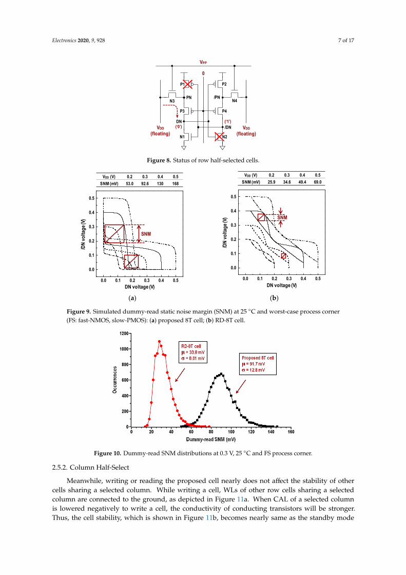
During write or read operation in our SRAM, CALs of other column cells sharing a selected roware connected to the ground, as depicted in Figure 8. Let us assume that DN holds ‘0’, while /DNholds ‘1’. When a row is selected, the voltage dividing in serial three devices (access transistor (N3),conducting transistor (P3) with poor ‘0’ passing, and drive transistor (N1)) extremely limits voltage
Electronics 2020, 9, 928 6 of 17
rising of DN, improving the dummy-read static noise margin (SNM). This is verified in the butterflycurve of Figure 9. When DN rises from ‘0’ to ‘1’ with BL = /BL = ‘1’ and WL = high, /DN changes from‘1’ to ‘0’. In this voltage transfer curve, the logic ‘0’ value of /DN node in our cell is nearly 0 V becauseof the conducting transistor. This provides a very ideal butterfly curve, preferable for stable SRAM.At VDD = 0.4 V and T = 25 ◦C, the dummy-read SNM of the proposed cell measures 130 mV, 2.6×higher than that of the RD-8T cell. Figure 10 shows the 10000 Monte Carlo simulation results at 0.3 V,25 ◦C and worst-case FS (fast-NMOS, slow-PMOS) process corner. The results show that the meanand minimum values of dummy-read SNM of the proposed cell are 2.7× and 3.5× higher than thoseof the RD-8T cell, respectively. As the stability of row half-selected cells is good enough, an efficientbit-interleaving architecture might be implemented in the proposed SRAM.
Electronics 2020, 9, x FOR PEER REVIEW 5 of 16
of the conducting PMOSs is sufficiently large, /DN can be easily discharged to ground. Falling of /DN brings the cross-coupled latch (P1-N1, P2-N2) to complete a flip of state.
Figure 5. Our cell status during write operation.
Besides the read stability, the write capability of SRAM is equally important for the subthreshold operation. In Figure 6, the write-ability of our cell is compared with the commercialized RD-8T cell at the worst-case process corner (SF: slow-NMOS, fast-PMOS). To write a SRAM cell, one of the bitlines needs to be discharged. The write margin (WM), a metric of the write-ability, is defined here as the discharging bitline voltage when a flip of cell state occurs. The larger the write margin, the easier to it is write. At VDD = 0.4 V and room temperature, WM of the proposed cell measures 177.3 mV, 3.6× larger than that of the RD-8T cell. This is because we boost the wordline by 30% of supply voltage to increase the conductivity of the access transistors. Such boosting provides strong write-ability even in the deep subthreshold region. The column-wise write-assist increasing the strength of the conducting transistors also facilitates changing the contents of the cell. On the contrary, the wordline boosting technique may not be employed on the RD-8T cell, because the stability of half-selected cells during write access is significantly degraded by the boosted write-wordline voltage. Figure 7 shows the WM distributions at 0.3 V, 25 °C and the worst-case SF process corner obtained from 10,000 Monte Carlo iterations. Statistically, our cell achieves 3.7× higher mean WM as compared with the RD-8T cell. The minimum WM, which is more critical in subthreshold SRAM design, is also 85 mV higher than that of the RD-8T cell. Overall, the proposed cell provides strong write-ability that results mainly from the wordline boosting and the column-wise write-assist.
(a) (b)
Figure 6. Simulated write-ability at 25 °C and SF process corner: (a) proposed 8T cell; (b) RD-8T cell. WM, write margin.
PN /PN
/DNDN
N1 N2
P2
N4
P3
NVGG
P4
(‘L’)(‘H’)
P1
N3
VDD 0
VPP
0.0 0.1 0.2 0.3 0.4 0.5
0.0
0.1
0.2
0.3
0.4
0.5
Bitline voltage (V)
Dat
a-no
de vo
ltage
(V)
/DN
WM
VDD (V) 0.2 0.3 0.4 0.5
WM (mV) 70.7 123.8 177.3 228.7
DN
/DN DN
VDD (V) 0.2 0.3 0.4 0.5
WM (mV) 15.3 32.0 48.6 68.3
0.0 0.1 0.2 0.3 0.4 0.5
0.0
0.1
0.2
0.3
0.4
0.5
Bitline voltage (V)
Dat
a-no
de vo
ltage
(V)
/DN DN
/DN DN
WM
Figure 6. Simulated write-ability at 25 ◦C and SF process corner: (a) proposed 8T cell; (b) RD-8T cell.WM, write margin.
Electronics 2020, 9, x FOR PEER REVIEW 6 of 16
Figure 7. Results of 10,000 MC simulations for WM (VDD = 0.3 V, T = 25 °C, SF process corner).
2.5. Half-Select Issue
2.5.1. Row Half-Select
An efficient bit-interleaving architecture may not be applicable to some previous low-voltage SRAMs [2–10]. While writing into a cell in these SRAMs, other column cells sharing a selected row experience dummy-read operation, degrading their hold stability significantly. To cope with the row half-select disturbance, we employed a cross-point access scheme.
During write or read operation in our SRAM, CALs of other column cells sharing a selected row are connected to the ground, as depicted in Figure 8. Let us assume that DN holds ’0’, while /DN holds ’1’. When a row is selected, the voltage dividing in serial three devices (access transistor (N3), conducting transistor (P3) with poor ‘0’ passing, and drive transistor (N1)) extremely limits voltage rising of DN, improving the dummy-read static noise margin (SNM). This is verified in the butterfly curve of Figure 9. When DN rises from ‘0’ to ‘1’ with BL = /BL = ‘1’ and WL = high, /DN changes from ‘1’ to ‘0’. In this voltage transfer curve, the logic ‘0’ value of /DN node in our cell is nearly 0 V because of the conducting transistor. This provides a very ideal butterfly curve, preferable for stable SRAM. At VDD = 0.4 V and T = 25 °C, the dummy-read SNM of the proposed cell measures 130 mV, 2.6× higher than that of the RD-8T cell. Figure 10 shows the 10000 Monte Carlo simulation results at 0.3 V, 25 °C and worst-case FS (fast-NMOS, slow-PMOS) process corner. The results show that the mean and minimum values of dummy-read SNM of the proposed cell are 2.7× and 3.5× higher than those of the RD-8T cell, respectively. As the stability of row half-selected cells is good enough, an efficient bit-interleaving architecture might be implemented in the proposed SRAM.
Figure 8. Status of row half-selected cells.
PN /PN
/DNDN
N1 N2
P2
N4
P3
0
P4
(‘0’)(‘1’)
P1
N3
VDD
(floating)VDD
(floating)
VPP
Figure 7. Results of 10,000 MC simulations for WM (VDD = 0.3 V, T = 25 ◦C, SF process corner).
Electronics 2020, 9, 928 7 of 17
Electronics 2020, 9, x FOR PEER REVIEW 6 of 16
Figure 7. Results of 10,000 MC simulations for WM (VDD = 0.3 V, T = 25 °C, SF process corner).
2.5. Half-Select Issue
2.5.1. Row Half-Select
An efficient bit-interleaving architecture may not be applicable to some previous low-voltage SRAMs [2–10]. While writing into a cell in these SRAMs, other column cells sharing a selected row experience dummy-read operation, degrading their hold stability significantly. To cope with the row half-select disturbance, we employed a cross-point access scheme.
During write or read operation in our SRAM, CALs of other column cells sharing a selected row are connected to the ground, as depicted in Figure 8. Let us assume that DN holds ’0’, while /DN holds ’1’. When a row is selected, the voltage dividing in serial three devices (access transistor (N3), conducting transistor (P3) with poor ‘0’ passing, and drive transistor (N1)) extremely limits voltage rising of DN, improving the dummy-read static noise margin (SNM). This is verified in the butterfly curve of Figure 9. When DN rises from ‘0’ to ‘1’ with BL = /BL = ‘1’ and WL = high, /DN changes from ‘1’ to ‘0’. In this voltage transfer curve, the logic ‘0’ value of /DN node in our cell is nearly 0 V because of the conducting transistor. This provides a very ideal butterfly curve, preferable for stable SRAM. At VDD = 0.4 V and T = 25 °C, the dummy-read SNM of the proposed cell measures 130 mV, 2.6× higher than that of the RD-8T cell. Figure 10 shows the 10000 Monte Carlo simulation results at 0.3 V, 25 °C and worst-case FS (fast-NMOS, slow-PMOS) process corner. The results show that the mean and minimum values of dummy-read SNM of the proposed cell are 2.7× and 3.5× higher than those of the RD-8T cell, respectively. As the stability of row half-selected cells is good enough, an efficient bit-interleaving architecture might be implemented in the proposed SRAM.
Figure 8. Status of row half-selected cells.
PN /PN
/DNDN
N1 N2
P2
N4
P3
0
P4
(‘0’)(‘1’)
P1
N3
VDD
(floating)VDD
(floating)
VPP
Figure 8. Status of row half-selected cells.Electronics 2020, 9, x FOR PEER REVIEW 7 of 16
(a) (b)
Figure 9. Simulated dummy-read static noise margin (SNM) at 25 °C and worst-case process corner (FS: fast-NMOS, slow-PMOS): (a) proposed 8T cell; (b) RD-8T cell.
Figure 10. Dummy-read SNM distributions at 0.3 V, 25 °C and FS process corner.
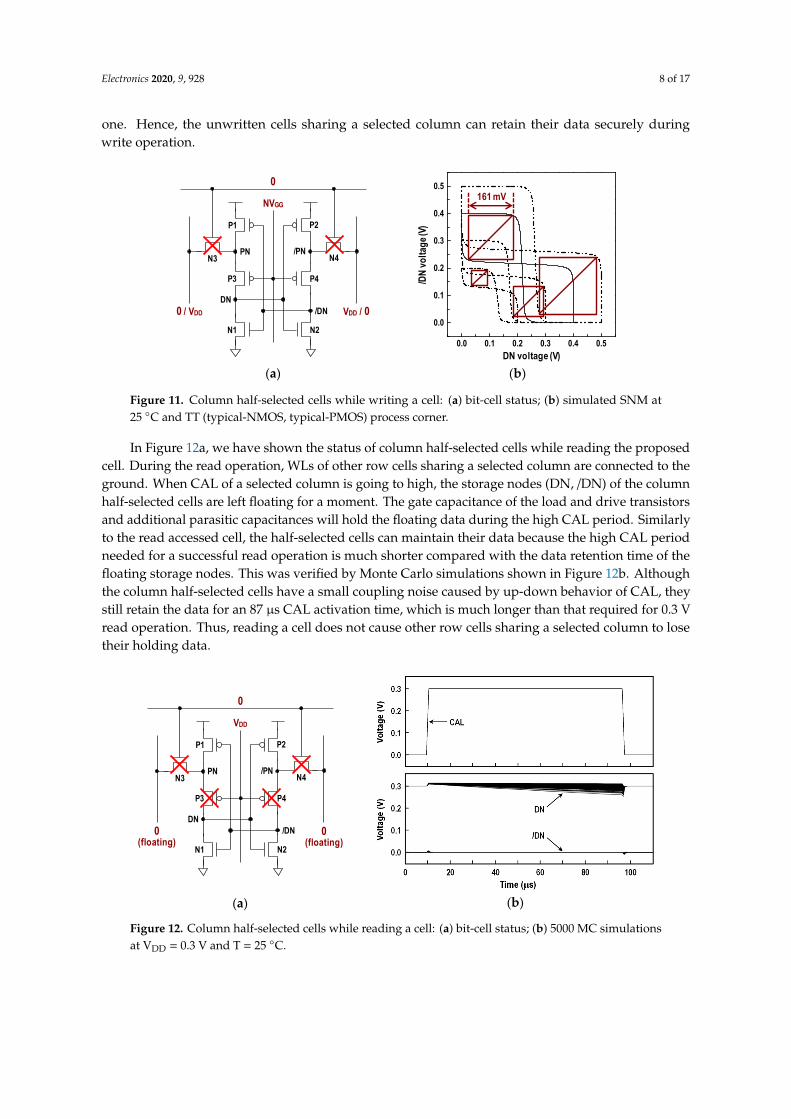
2.5.2. Column Half-Select
Meanwhile, writing or reading the proposed cell nearly does not affect the stability of other cells sharing a selected column. While writing a cell, WLs of other row cells sharing a selected column are connected to the ground, as depicted in Figure 11a. When CAL of a selected column is lowered negatively to write a cell, the conductivity of conducting transistors will be stronger. Thus, the cell stability, which is shown in Figure 11b, becomes nearly same as the standby mode one. Hence, the unwritten cells sharing a selected column can retain their data securely during write operation.
In Figure 12a, we have shown the status of column half-selected cells while reading the proposed cell. During the read operation, WLs of other row cells sharing a selected column are connected to the ground. When CAL of a selected column is going to high, the storage nodes (DN, /DN) of the column half-selected cells are left floating for a moment. The gate capacitance of the load and drive transistors and additional parasitic capacitances will hold the floating data during the high CAL period. Similarly to the read accessed cell, the half-selected cells can maintain their data because the high CAL period needed for a successful read operation is much shorter compared with the data retention time of the floating storage nodes. This was verified by Monte Carlo simulations shown in Figure 12b. Although the column half-selected cells have a small coupling noise caused by up-down behavior of CAL, they still retain the data for an 87 µs CAL activation time, which is much longer than that required for 0.3 V read operation. Thus, reading a cell does not cause other row cells sharing a selected column to lose their holding data.
0.0 0.1 0.2 0.3 0.4 0.5
0.0
0.1
0.2
0.3
0.4
0.5
/D
N v
olta
ge (V
)
DN voltage (V)
VDD (V) 0.2 0.3 0.4 0.5
SNM (mV) 53.0 92.6 130 168
SNM
0.0 0.1 0.2 0.3 0.4 0.5
0.0
0.1
0.2
0.3
0.4
0.5
VDD (V) 0.2 0.3 0.4 0.5
SNM (mV) 25.9 34.6 49.4 69.0
/DN
vol
tage
(V)
DN voltage (V)
SNM
Figure 9. Simulated dummy-read static noise margin (SNM) at 25 ◦C and worst-case process corner(FS: fast-NMOS, slow-PMOS): (a) proposed 8T cell; (b) RD-8T cell.
Electronics 2020, 9, x FOR PEER REVIEW 7 of 16
(a) (b)
Figure 9. Simulated dummy-read static noise margin (SNM) at 25 °C and worst-case process corner (FS: fast-NMOS, slow-PMOS): (a) proposed 8T cell; (b) RD-8T cell.
Figure 10. Dummy-read SNM distributions at 0.3 V, 25 °C and FS process corner.
2.5.2. Column Half-Select
Meanwhile, writing or reading the proposed cell nearly does not affect the stability of other cells sharing a selected column. While writing a cell, WLs of other row cells sharing a selected column are connected to the ground, as depicted in Figure 11a. When CAL of a selected column is lowered negatively to write a cell, the conductivity of conducting transistors will be stronger. Thus, the cell stability, which is shown in Figure 11b, becomes nearly same as the standby mode one. Hence, the unwritten cells sharing a selected column can retain their data securely during write operation.
In Figure 12a, we have shown the status of column half-selected cells while reading the proposed cell. During the read operation, WLs of other row cells sharing a selected column are connected to the ground. When CAL of a selected column is going to high, the storage nodes (DN, /DN) of the column half-selected cells are left floating for a moment. The gate capacitance of the load and drive transistors and additional parasitic capacitances will hold the floating data during the high CAL period. Similarly to the read accessed cell, the half-selected cells can maintain their data because the high CAL period needed for a successful read operation is much shorter compared with the data retention time of the floating storage nodes. This was verified by Monte Carlo simulations shown in Figure 12b. Although the column half-selected cells have a small coupling noise caused by up-down behavior of CAL, they still retain the data for an 87 µs CAL activation time, which is much longer than that required for 0.3 V read operation. Thus, reading a cell does not cause other row cells sharing a selected column to lose their holding data.
0.0 0.1 0.2 0.3 0.4 0.5
0.0
0.1
0.2
0.3
0.4
0.5
/D
N v
olta
ge (V
)
DN voltage (V)
VDD (V) 0.2 0.3 0.4 0.5
SNM (mV) 53.0 92.6 130 168
SNM
0.0 0.1 0.2 0.3 0.4 0.5
0.0
0.1
0.2
0.3
0.4
0.5
VDD (V) 0.2 0.3 0.4 0.5
SNM (mV) 25.9 34.6 49.4 69.0
/DN
vol
tage
(V)
DN voltage (V)
SNM
Figure 10. Dummy-read SNM distributions at 0.3 V, 25 ◦C and FS process corner.
2.5.2. Column Half-Select
Meanwhile, writing or reading the proposed cell nearly does not affect the stability of othercells sharing a selected column. While writing a cell, WLs of other row cells sharing a selectedcolumn are connected to the ground, as depicted in Figure 11a. When CAL of a selected columnis lowered negatively to write a cell, the conductivity of conducting transistors will be stronger.Thus, the cell stability, which is shown in Figure 11b, becomes nearly same as the standby mode
Electronics 2020, 9, 928 8 of 17
one. Hence, the unwritten cells sharing a selected column can retain their data securely duringwrite operation.Electronics 2020, 9, x FOR PEER REVIEW 8 of 16
(a) (b)
Figure 11. Column half-selected cells while writing a cell: (a) bit-cell status; (b) simulated SNM at 25 °C and TT (typical-NMOS, typical-PMOS) process corner.
(a) (b)
Figure 12. Column half-selected cells while reading a cell: (a) bit-cell status; (b) 5000 MC simulations at VDD = 0.3 V and T = 25 °C.
3. Macro Design
3.1. Macro Organization
To verify the proposed SRAM cell and its subthreshold operation, we implemented a 32-kbit SRAM macro with an industrial 180 nm low-power CMOS process. Figure 13 shows its basic schematic diagram. The 32-kbit memory macro consists of two 16-kbit memory blocks. Each block contains 128-row × 128-column array. The I/O is eight bits wide. In this design, each high capacitive bitline pair has a local sense amplifier (SA) to reduce the read delay under deep-low voltage regime. During read access, the bitline SAs forward the full-swing read signals to the block sense amplifiers dedicated to each 16-kbit block. In addition, the macro includes two wordline boosters dedicated to each 16-kbit block and one negative voltage generator supplying the NVGG voltage. The write drivers; column signal drivers; and other peripheral units like address buffers, control buffers, data I/O buffers, predecoders, and control logic use static CMOS circuits. The whole memory macro operates at single supply voltage.
PN /PN
/DNDN
N1 N2
P2
N4
P3
NVGG
P4
P1
N3
0 / VDD VDD / 0
0
0.0 0.1 0.2 0.3 0.4 0.5
0.0
0.1
0.2
0.3
0.4
0.5
/D
N v
olta
ge (V
)
DN voltage (V)
161 mV
PN /PN
/DNDN
N1 N2
P2
N4
P3
VDD
P4
P1
N3
0
0(floating)
0(floating)
Figure 11. Column half-selected cells while writing a cell: (a) bit-cell status; (b) simulated SNM at25 ◦C and TT (typical-NMOS, typical-PMOS) process corner.
In Figure 12a, we have shown the status of column half-selected cells while reading the proposedcell. During the read operation, WLs of other row cells sharing a selected column are connected to theground. When CAL of a selected column is going to high, the storage nodes (DN, /DN) of the columnhalf-selected cells are left floating for a moment. The gate capacitance of the load and drive transistorsand additional parasitic capacitances will hold the floating data during the high CAL period. Similarlyto the read accessed cell, the half-selected cells can maintain their data because the high CAL periodneeded for a successful read operation is much shorter compared with the data retention time of thefloating storage nodes. This was verified by Monte Carlo simulations shown in Figure 12b. Althoughthe column half-selected cells have a small coupling noise caused by up-down behavior of CAL, theystill retain the data for an 87 µs CAL activation time, which is much longer than that required for 0.3 Vread operation. Thus, reading a cell does not cause other row cells sharing a selected column to losetheir holding data.
Electronics 2020, 9, x FOR PEER REVIEW 8 of 16
(a) (b)
Figure 11. Column half-selected cells while writing a cell: (a) bit-cell status; (b) simulated SNM at 25 °C and TT (typical-NMOS, typical-PMOS) process corner.
(a) (b)
Figure 12. Column half-selected cells while reading a cell: (a) bit-cell status; (b) 5000 MC simulations at VDD = 0.3 V and T = 25 °C.
3. Macro Design
3.1. Macro Organization
To verify the proposed SRAM cell and its subthreshold operation, we implemented a 32-kbit SRAM macro with an industrial 180 nm low-power CMOS process. Figure 13 shows its basic schematic diagram. The 32-kbit memory macro consists of two 16-kbit memory blocks. Each block contains 128-row × 128-column array. The I/O is eight bits wide. In this design, each high capacitive bitline pair has a local sense amplifier (SA) to reduce the read delay under deep-low voltage regime. During read access, the bitline SAs forward the full-swing read signals to the block sense amplifiers dedicated to each 16-kbit block. In addition, the macro includes two wordline boosters dedicated to each 16-kbit block and one negative voltage generator supplying the NVGG voltage. The write drivers; column signal drivers; and other peripheral units like address buffers, control buffers, data I/O buffers, predecoders, and control logic use static CMOS circuits. The whole memory macro operates at single supply voltage.
PN /PN
/DNDN
N1 N2
P2
N4
P3
NVGG
P4
P1
N3
0 / VDD VDD / 0
0
0.0 0.1 0.2 0.3 0.4 0.5
0.0
0.1
0.2
0.3
0.4
0.5
/D
N v
olta
ge (V
)
DN voltage (V)
161 mV
PN /PN
/DNDN
N1 N2
P2
N4
P3
VDD
P4
P1
N3
0
0(floating)
0(floating)
Figure 12. Column half-selected cells while reading a cell: (a) bit-cell status; (b) 5000 MC simulationsat VDD = 0.3 V and T = 25 ◦C.

Electronics 2020, 9, 928 9 of 17
3. Macro Design
3.1. Macro Organization
To verify the proposed SRAM cell and its subthreshold operation, we implemented a 32-kbitSRAM macro with an industrial 180 nm low-power CMOS process. Figure 13 shows its basic schematicdiagram. The 32-kbit memory macro consists of two 16-kbit memory blocks. Each block contains128-row × 128-column array. The I/O is eight bits wide. In this design, each high capacitive bitline pairhas a local sense amplifier (SA) to reduce the read delay under deep-low voltage regime. During readaccess, the bitline SAs forward the full-swing read signals to the block sense amplifiers dedicated to each16-kbit block. In addition, the macro includes two wordline boosters dedicated to each 16-kbit blockand one negative voltage generator supplying the NVGG voltage. The write drivers; column signaldrivers; and other peripheral units like address buffers, control buffers, data I/O buffers, predecoders,and control logic use static CMOS circuits. The whole memory macro operates at single supply voltage.Electronics 2020, 9, x FOR PEER REVIEW 9 of 16
Figure 13. Block diagram of 32-kbit SRAM macro. SA, sense amplifier.
3.2. Cell Array Architecture
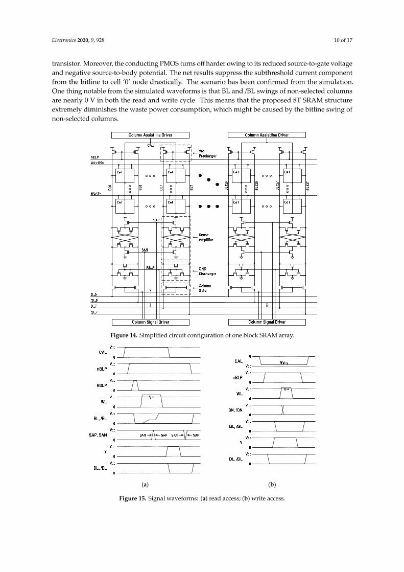
Figure 14 shows the configuration of one block SRAM array, and Figure 15 illustrates its read and write signal waveforms. The design employs an eight-column activating architecture to minimize the array power consumption. During the standby, the bitline pairs and datalines (DL, /DL) are precharged to VDD, and WL and CAL are connected to ground.
Figure 14. Simplified circuit configuration of one block SRAM array.
ACOL(7~11)
AROW(0~6)
PreDecoder
RowAddressBuffer
ColumnAddressBuffer
WE Buffer
CS Buffer
ControlLogic
ColumnSignal Driver
RowDecoder
/WE
CLK
NegativeVoltage
Generator
/CS
WordlineBooster
2×16-kbitCell Array
SA / Discharger / Col-Gate
VDD PrechargerColumn Assistline Driver
Write Driver / Block Sense Amplifier
Data In/Out Buffer
DOUT(0~7)DIN(0~7)
/ZZ
Figure 13. Block diagram of 32-kbit SRAM macro. SA, sense amplifier.
3.2. Cell Array Architecture
Figure 14 shows the configuration of one block SRAM array, and Figure 15 illustrates its read andwrite signal waveforms. The design employs an eight-column activating architecture to minimize thearray power consumption. During the standby, the bitline pairs and datalines (DL, /DL) are prechargedto VDD, and WL and CAL are connected to ground.
In the read access, the conducting transistors of accessed cells are turned off by switching CALto high, and the VDD prechargers are disabled. Next, the selected bitlines are discharged to groundand then floated by toggling RBLP signal. To read out each stored value of the selected cells, WL isswitched to VPP. The cell read-current charges one of the bitlines depending on the stored information.Then, the sense amplifiers are enabled by triggering SAN and SAP. After WL is switched to ground,the column gates are turned on to transfer the read signals to the datalines.
In the write access, the external data drive the datalines. After lowering CAL to a negative voltageNVGG, the VDD prechargers are disabled. Next, BL and /BL are driven with the external data by raisinga column signal Y. Then, WL is switched to VPP, allowing the external data to be written. After WLand Y return to ground, the bitlines are charged to VDD, and CAL is switched to ground.
In Figure 16, we show a natural benefit of the proposed cell structure. During the read or writecycle, CALs of row half-selected cells within a 128-row × 128-column array are connected to the ground.When a WL is activated, the row half-selected cells may discharge the bilines. However, the currentpath from VDD-precharged bitline to data ‘0’ node suffers a stack effect because of the conducting
Electronics 2020, 9, 928 10 of 17
transistor. Moreover, the conducting PMOS turns off harder owing to its reduced source-to-gate voltageand negative source-to-body potential. The net results suppress the subthreshold current componentfrom the bitline to cell ‘0’ node drastically. The scenario has been confirmed from the simulation.One thing notable from the simulated waveforms is that BL and /BL swings of non-selected columnsare nearly 0 V in both the read and write cycle. This means that the proposed 8T SRAM structureextremely diminishes the waste power consumption, which might be caused by the bitline swing ofnon-selected columns.
Electronics 2020, 9, x FOR PEER REVIEW 9 of 16
Figure 13. Block diagram of 32-kbit SRAM macro. SA, sense amplifier.
3.2. Cell Array Architecture
Figure 14 shows the configuration of one block SRAM array, and Figure 15 illustrates its read and write signal waveforms. The design employs an eight-column activating architecture to minimize the array power consumption. During the standby, the bitline pairs and datalines (DL, /DL) are precharged to VDD, and WL and CAL are connected to ground.
Figure 14. Simplified circuit configuration of one block SRAM array.
ACOL(7~11)
AROW(0~6)
PreDecoder
RowAddressBuffer
ColumnAddressBuffer
WE Buffer
CS Buffer
ControlLogic
ColumnSignal Driver
RowDecoder
/WE
CLK
NegativeVoltage
Generator
/CS
WordlineBooster
2×16-kbitCell Array
SA / Discharger / Col-Gate
VDD PrechargerColumn Assistline Driver
Write Driver / Block Sense Amplifier
Data In/Out Buffer
DOUT(0~7)DIN(0~7)
/ZZ
Figure 14. Simplified circuit configuration of one block SRAM array.Electronics 2020, 9, x FOR PEER REVIEW 10 of 16
(a) (b)
Figure 15. Signal waveforms: (a) read access; (b) write access.
In the read access, the conducting transistors of accessed cells are turned off by switching CAL to high, and the VDD prechargers are disabled. Next, the selected bitlines are discharged to ground and then floated by toggling RBLP signal. To read out each stored value of the selected cells, WL is switched to VPP. The cell read-current charges one of the bitlines depending on the stored information. Then, the sense amplifiers are enabled by triggering SAN and SAP. After WL is switched to ground, the column gates are turned on to transfer the read signals to the datalines.
In the write access, the external data drive the datalines. After lowering CAL to a negative voltage NVGG, the VDD prechargers are disabled. Next, BL and /BL are driven with the external data by raising a column signal Y. Then, WL is switched to VPP, allowing the external data to be written. After WL and Y return to ground, the bitlines are charged to VDD, and CAL is switched to ground.
In Figure 16, we show a natural benefit of the proposed cell structure. During the read or write cycle, CALs of row half-selected cells within a 128-row × 128-column array are connected to the ground. When a WL is activated, the row half-selected cells may discharge the bilines. However, the current path from VDD-precharged bitline to data ‘0’ node suffers a stack effect because of the conducting transistor. Moreover, the conducting PMOS turns off harder owing to its reduced source-to-gate voltage and negative source-to-body potential. The net results suppress the subthreshold current component from the bitline to cell ‘0’ node drastically. The scenario has been confirmed from the simulation. One thing notable from the simulated waveforms is that BL and /BL swings of non-selected columns are nearly 0 V in both the read and write cycle. This means that the proposed 8T SRAM structure extremely diminishes the waste power consumption, which might be caused by the bitline swing of non-selected columns.
3.3. Wordline Booster
Figure 17 shows the row path circuitry used in this work. The wordline booster providing a boosted voltage VPP was implemented with a traditional circuit using one boosting capacitor (CVPP). The booster output WBOUT is the supply node of 128 row decoders. Each row decoder consists of a static CMOS gate followed by a level shifter. During standby, the node WBOUT is connected to VDD. Whenever write or read operation is performed, the control signal VPPPRE with positive transition makes WBOUT float. The succeeding control signal VPPEN with positive transition allows the boosting capacitor to push the voltage of WBOUT node above VDD. Then, a selected row decoder transfers the boosted VPP level (about 1.3VDD in this design) to the wordline.
Figure 15. Signal waveforms: (a) read access; (b) write access.

Electronics 2020, 9, 928 11 of 17Electronics 2020, 9, x FOR PEER REVIEW 11 of 16
(a) (b) Figure 16. Natural benefit of our cell structure: (a) bitline discharging current path in the row half-selected cells; (b) simulated waveforms at VDD = 0.4 V.
Figure 17. Wordline booster together with 128 row decoders.
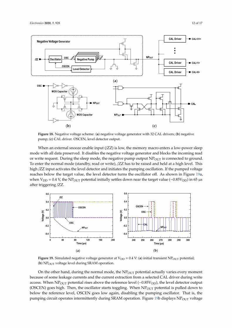
3.4. Negative Voltage Generator
Figure 18 shows our negative voltage scheme providing a negative voltage NVGG. The negative voltage generator in this work consists of an oscillator, negative charge pump utilizing voltage doubler [21], and level detector. The negative pump has two charge-transfer paths. During one oscillation period, the pump transfers charges alternately.
When an external snooze enable input (/ZZ) is low, the memory macro enters a low-power sleep mode with all data preserved. It disables the negative voltage generator and blocks the incoming read or write request. During the sleep mode, the negative pump output NPOUT is connected to ground. To enter the normal mode (standby, read or write), /ZZ has to be raised and held at a high level. This high /ZZ input activates the level detector and initiates the pumping oscillation. If the pumped voltage reaches below the target value, the level detector turns the oscillator off. As shown in Figure 19a, when VDD = 0.4 V, the NPOUT potential initially settles down near the target value (−0.85VDD) in 65 µs after triggering /ZZ.
On the other hand, during the normal mode, the NPOUT potential actually varies every moment because of some leakage currents and the current extraction from a selected CAL driver during write access. When NPOUT potential rises above the reference level (−0.85VDD), the level detector output (OSCEN) goes high. Then, the oscillator starts toggling. When NPOUT potential is pulled down to below the reference level, OSCEN goes low again, disabling the pumping oscillator. That is, the pumping circuit operates intermittently during SRAM operation. Figure 19b displays NPOUT voltage
≠0
VPP
VDD
(floating) 0 VDD
VDD
(floating)
VDD
0
0.00.20.4
0.0
0.2
0.4
0.0
0.2
0.40.0
0.2
0.4
0.0
0.2
0.4
Time (μs)
Volta
ge (V
)
WL
55 60 65 70 75
BL0, /BL0
DN0, /DN0
BL8, /BL8
DN8, /DN8
Read Write Read Write
Figure 16. Natural benefit of our cell structure: (a) bitline discharging current path in the rowhalf-selected cells; (b) simulated waveforms at VDD = 0.4 V.
3.3. Wordline Booster
Figure 17 shows the row path circuitry used in this work. The wordline booster providing aboosted voltage VPP was implemented with a traditional circuit using one boosting capacitor (CVPP).The booster output WBOUT is the supply node of 128 row decoders. Each row decoder consists of astatic CMOS gate followed by a level shifter. During standby, the node WBOUT is connected to VDD.Whenever write or read operation is performed, the control signal VPPPRE with positive transitionmakes WBOUT float. The succeeding control signal VPPEN with positive transition allows the boostingcapacitor to push the voltage of WBOUT node above VDD. Then, a selected row decoder transfers theboosted VPP level (about 1.3VDD in this design) to the wordline.
Electronics 2020, 9, x FOR PEER REVIEW 11 of 16
(a) (b) Figure 16. Natural benefit of our cell structure: (a) bitline discharging current path in the row half-selected cells; (b) simulated waveforms at VDD = 0.4 V.
Figure 17. Wordline booster together with 128 row decoders.
3.4. Negative Voltage Generator
Figure 18 shows our negative voltage scheme providing a negative voltage NVGG. The negative voltage generator in this work consists of an oscillator, negative charge pump utilizing voltage doubler [21], and level detector. The negative pump has two charge-transfer paths. During one oscillation period, the pump transfers charges alternately.
When an external snooze enable input (/ZZ) is low, the memory macro enters a low-power sleep mode with all data preserved. It disables the negative voltage generator and blocks the incoming read or write request. During the sleep mode, the negative pump output NPOUT is connected to ground. To enter the normal mode (standby, read or write), /ZZ has to be raised and held at a high level. This high /ZZ input activates the level detector and initiates the pumping oscillation. If the pumped voltage reaches below the target value, the level detector turns the oscillator off. As shown in Figure 19a, when VDD = 0.4 V, the NPOUT potential initially settles down near the target value (−0.85VDD) in 65 µs after triggering /ZZ.
On the other hand, during the normal mode, the NPOUT potential actually varies every moment because of some leakage currents and the current extraction from a selected CAL driver during write access. When NPOUT potential rises above the reference level (−0.85VDD), the level detector output (OSCEN) goes high. Then, the oscillator starts toggling. When NPOUT potential is pulled down to below the reference level, OSCEN goes low again, disabling the pumping oscillator. That is, the pumping circuit operates intermittently during SRAM operation. Figure 19b displays NPOUT voltage
≠0
VPP
VDD
(floating) 0 VDD
VDD
(floating)
VDD
0
0.00.20.4
0.0
0.2
0.4
0.0
0.2
0.40.0
0.2
0.4
0.0
0.2
0.4
Time (μs)
Volta
ge (V
)
WL
55 60 65 70 75
BL0, /BL0
DN0, /DN0
BL8, /BL8
DN8, /DN8
Read Write Read Write
Figure 17. Wordline booster together with 128 row decoders.
3.4. Negative Voltage Generator
Figure 18 shows our negative voltage scheme providing a negative voltage NVGG. The negativevoltage generator in this work consists of an oscillator, negative charge pump utilizing voltagedoubler [21], and level detector. The negative pump has two charge-transfer paths. During oneoscillation period, the pump transfers charges alternately.
Electronics 2020, 9, 928 12 of 17
Electronics 2020, 9, x FOR PEER REVIEW 12 of 16
variation under successive write operation with a period of 6.2 µs. As shown in the simulation, the negative voltage generator in this work can hold the NPOUT voltage level to the target value (−0.34 V for VDD = 0.4 V) with the maximum deviation of ±12 mV.
(a)
(b) (c)
Figure 18. Negative voltage scheme: (a) negative voltage generator with 32 CAL drivers; (b) negative pump; (c) CAL driver. OSCEN, level detector output.
(a) (b)
Figure 19. Simulated negative voltage generator at VDD = 0.4 V: (a) initial transient NPOUT potential; (b) NPOUT voltage level during SRAM operation.
4. Design Results
Figure 20 shows the CAD plot of SRAM layout. The 32-kbit macro was partitioned into two 16-kbit blocks. The wordline decoding circuits are located between the two memory blocks. The organization is 4096-word × 8-bit. The on-chip negative voltage generator is placed over the memory blocks. The wordline boosters, write drivers, block sense amplifiers, and other peripheral units are placed on the bottom. The macro size is 700 × 784 µm2. The layout area overhead incurred by two wordline boosters is 0.41% of the macro size, while one negative voltage generator together with 32 CAL drivers (shown in Figure 18) consumes 4.75% of the macro area.
NPOUT
CAL Driver CAL<1>
CAL Driver CAL<31>
Oscillator Negative Pump
Level Detector
/ZZ
OSCEN
OSC
Negative Voltage Generator
CAL Driver CAL<0>
MOS Capacitor
OSC
NPOUT
MOS Capacitor
NPOUT
OSCEN
/ZZ
Time (μs)0 40 80 120 160 200
Volta
ge (V
)
-0.4
-0.2
0.0
0.2
0.4
0.6
OSC
OSCEN
Time (μs)280 290 300
Volta
ge (V
)
-0.4
-0.2
0.0
0.2
0.4
0.6
270260250240
OSC
CALNPOUT
Figure 18. Negative voltage scheme: (a) negative voltage generator with 32 CAL drivers; (b) negativepump; (c) CAL driver. OSCEN, level detector output.
When an external snooze enable input (/ZZ) is low, the memory macro enters a low-power sleepmode with all data preserved. It disables the negative voltage generator and blocks the incoming reador write request. During the sleep mode, the negative pump output NPOUT is connected to ground.To enter the normal mode (standby, read or write), /ZZ has to be raised and held at a high level. Thishigh /ZZ input activates the level detector and initiates the pumping oscillation. If the pumped voltagereaches below the target value, the level detector turns the oscillator off. As shown in Figure 19a,when VDD = 0.4 V, the NPOUT potential initially settles down near the target value (−0.85VDD) in 65 µsafter triggering /ZZ.
Electronics 2020, 9, x FOR PEER REVIEW 12 of 16
variation under successive write operation with a period of 6.2 µs. As shown in the simulation, the negative voltage generator in this work can hold the NPOUT voltage level to the target value (−0.34 V for VDD = 0.4 V) with the maximum deviation of ±12 mV.
(a)
(b) (c)
Figure 18. Negative voltage scheme: (a) negative voltage generator with 32 CAL drivers; (b) negative pump; (c) CAL driver. OSCEN, level detector output.
(a) (b)
Figure 19. Simulated negative voltage generator at VDD = 0.4 V: (a) initial transient NPOUT potential; (b) NPOUT voltage level during SRAM operation.
4. Design Results
Figure 20 shows the CAD plot of SRAM layout. The 32-kbit macro was partitioned into two 16-kbit blocks. The wordline decoding circuits are located between the two memory blocks. The organization is 4096-word × 8-bit. The on-chip negative voltage generator is placed over the memory blocks. The wordline boosters, write drivers, block sense amplifiers, and other peripheral units are placed on the bottom. The macro size is 700 × 784 µm2. The layout area overhead incurred by two wordline boosters is 0.41% of the macro size, while one negative voltage generator together with 32 CAL drivers (shown in Figure 18) consumes 4.75% of the macro area.
NPOUT
CAL Driver CAL<1>
CAL Driver CAL<31>
Oscillator Negative Pump
Level Detector
/ZZ
OSCEN
OSC
Negative Voltage Generator
CAL Driver CAL<0>
MOS Capacitor
OSC
NPOUT
MOS Capacitor
NPOUT
OSCEN
/ZZ
Time (μs)0 40 80 120 160 200
Volta
ge (V
)
-0.4
-0.2
0.0
0.2
0.4
0.6
OSC
OSCEN
Time (μs)280 290 300
Volta
ge (V
)
-0.4
-0.2
0.0
0.2
0.4
0.6
270260250240
OSC
CALNPOUT
Figure 19. Simulated negative voltage generator at VDD = 0.4 V: (a) initial transient NPOUT potential;(b) NPOUT voltage level during SRAM operation.
On the other hand, during the normal mode, the NPOUT potential actually varies every momentbecause of some leakage currents and the current extraction from a selected CAL driver during writeaccess. When NPOUT potential rises above the reference level (−0.85VDD), the level detector output(OSCEN) goes high. Then, the oscillator starts toggling. When NPOUT potential is pulled down tobelow the reference level, OSCEN goes low again, disabling the pumping oscillator. That is, thepumping circuit operates intermittently during SRAM operation. Figure 19b displays NPOUT voltage
Electronics 2020, 9, 928 13 of 17
variation under successive write operation with a period of 6.2 µs. As shown in the simulation,the negative voltage generator in this work can hold the NPOUT voltage level to the target value(−0.34 V for VDD = 0.4 V) with the maximum deviation of ±12 mV.
4. Design Results
Figure 20 shows the CAD plot of SRAM layout. The 32-kbit macro was partitioned into two 16-kbitblocks. The wordline decoding circuits are located between the two memory blocks. The organizationis 4096-word × 8-bit. The on-chip negative voltage generator is placed over the memory blocks.The wordline boosters, write drivers, block sense amplifiers, and other peripheral units are placed onthe bottom. The macro size is 700 × 784 µm2. The layout area overhead incurred by two wordlineboosters is 0.41% of the macro size, while one negative voltage generator together with 32 CAL drivers(shown in Figure 18) consumes 4.75% of the macro area.
Electronics 2020, 9, x FOR PEER REVIEW 13 of 16
Figure 20. CAD plot of 32-kbit subthreshold 8T SRAM.
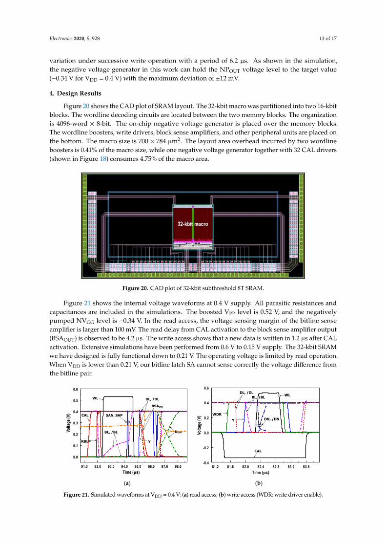
Figure 21 shows the internal voltage waveforms at 0.4 V supply. All parasitic resistances and capacitances are included in the simulations. The boosted VPP level is 0.52 V, and the negatively pumped NVGG level is −0.34 V. In the read access, the voltage sensing margin of the bitline sense amplifier is larger than 100 mV. The read delay from CAL activation to the block sense amplifier output (BSAOUT) is observed to be 4.2 µs. The write access shows that a new data is written in 1.2 µs after CAL activation. Extensive simulations have been performed from 0.6 V to 0.15 V supply. The 32-kbit SRAM we have designed is fully functional down to 0.21 V. The operating voltage is limited by read operation. When VDD is lower than 0.21 V, our bitline latch SA cannot sense correctly the voltage difference from the bitline pair.
(a) (b)
Figure 21. Simulated waveforms at VDD = 0.4 V: (a) read access; (b) write access (WDR: write driver enable).
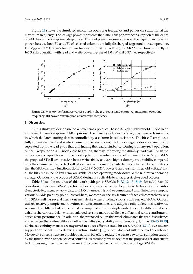
Figure 22 shows the simulated maximum operating frequency and power consumption at the maximum frequency. The leakage power represents the static leakage power consumption of the entire SRAM during the low-power sleep mode. The read power consumption is a little larger than the write power, because both BL and /BL of selected columns are fully discharged to ground in read operation. For VDD = 0.4 V (~80 mV lower than transistor threshold voltage), the SRAM functions correctly at 161.3 kHz operation with read and write power figures of 1.0 µW and 0.97 µW, respectively.
DOUT
WL
CAL
RBLP
DL, /DL
SAN, SAP
BL, /BL
BSAOUT
Y
Time (μs)91.0 92.0 93.0 94.0 95.0 98.096.0 97.0
Volta
ge (V
)
0.0
0.1
0.2
0.3
0.4
0.6
0.5
Time (μs)81.2 81.6 82.0 82.4 82.8 83.2 83.6
Volta
ge (V
)
-0.4
-0.2
0.0
0.2
0.6
0.4
WL
CAL
WDR
DL, /DL
Y DN, /DN
BL, /BL
Figure 20. CAD plot of 32-kbit subthreshold 8T SRAM.
Figure 21 shows the internal voltage waveforms at 0.4 V supply. All parasitic resistances andcapacitances are included in the simulations. The boosted VPP level is 0.52 V, and the negativelypumped NVGG level is −0.34 V. In the read access, the voltage sensing margin of the bitline senseamplifier is larger than 100 mV. The read delay from CAL activation to the block sense amplifier output(BSAOUT) is observed to be 4.2 µs. The write access shows that a new data is written in 1.2 µs after CALactivation. Extensive simulations have been performed from 0.6 V to 0.15 V supply. The 32-kbit SRAMwe have designed is fully functional down to 0.21 V. The operating voltage is limited by read operation.When VDD is lower than 0.21 V, our bitline latch SA cannot sense correctly the voltage difference fromthe bitline pair.
Electronics 2020, 9, x FOR PEER REVIEW 13 of 16
Figure 20. CAD plot of 32-kbit subthreshold 8T SRAM.
Figure 21 shows the internal voltage waveforms at 0.4 V supply. All parasitic resistances and capacitances are included in the simulations. The boosted VPP level is 0.52 V, and the negatively pumped NVGG level is −0.34 V. In the read access, the voltage sensing margin of the bitline sense amplifier is larger than 100 mV. The read delay from CAL activation to the block sense amplifier output (BSAOUT) is observed to be 4.2 µs. The write access shows that a new data is written in 1.2 µs after CAL activation. Extensive simulations have been performed from 0.6 V to 0.15 V supply. The 32-kbit SRAM we have designed is fully functional down to 0.21 V. The operating voltage is limited by read operation. When VDD is lower than 0.21 V, our bitline latch SA cannot sense correctly the voltage difference from the bitline pair.
(a) (b)
Figure 21. Simulated waveforms at VDD = 0.4 V: (a) read access; (b) write access (WDR: write driver enable).
Figure 22 shows the simulated maximum operating frequency and power consumption at the maximum frequency. The leakage power represents the static leakage power consumption of the entire SRAM during the low-power sleep mode. The read power consumption is a little larger than the write power, because both BL and /BL of selected columns are fully discharged to ground in read operation. For VDD = 0.4 V (~80 mV lower than transistor threshold voltage), the SRAM functions correctly at 161.3 kHz operation with read and write power figures of 1.0 µW and 0.97 µW, respectively.
DOUT
WL
CAL
RBLP
DL, /DL
SAN, SAP
BL, /BL
BSAOUT
Y
Time (μs)91.0 92.0 93.0 94.0 95.0 98.096.0 97.0
Volta
ge (V
)
0.0
0.1
0.2
0.3
0.4
0.6
0.5
Time (μs)81.2 81.6 82.0 82.4 82.8 83.2 83.6
Volta
ge (V
)
-0.4
-0.2
0.0
0.2
0.6
0.4
WL
CAL
WDR
DL, /DL
Y DN, /DN
BL, /BL
Figure 21. Simulated waveforms at VDD = 0.4 V: (a) read access; (b) write access (WDR: write driver enable).
Electronics 2020, 9, 928 14 of 17
Figure 22 shows the simulated maximum operating frequency and power consumption at themaximum frequency. The leakage power represents the static leakage power consumption of the entireSRAM during the low-power sleep mode. The read power consumption is a little larger than the writepower, because both BL and /BL of selected columns are fully discharged to ground in read operation.For VDD = 0.4 V (~80 mV lower than transistor threshold voltage), the SRAM functions correctly at161.3 kHz operation with read and write power figures of 1.0 µW and 0.97 µW, respectively.Electronics 2020, 9, x FOR PEER REVIEW 14 of 16
(a) (b)
Figure 22. Memory performance versus supply voltage at room temperature: (a) maximum operating frequency; (b) power consumption at maximum frequency.
5. Discussion
In this study, we demonstrated a novel cross-point cell based 32-kbit subthreshold SRAM in an industrial 180 nm low-power CMOS process. The memory cell consists of eight symmetric transistors, in which the latch storing data is controlled by a column-based assistline. The bit-cell employs a fully differential read and write scheme. In the read access, the true storage nodes are dynamically separated from the read path, thus eliminating the read disturbance. During dummy-read operation, our cell keeps the data ‘0’ node close to ground, thereby improving the dummy-read stability. In the write access, a capacitive wordline boosting technique enhances the cell write-ability. At VDD = 0.4 V, the proposed 8T cell achieves 3.6× better write-ability and 2.6× higher dummy-read stability compared with the commercialized RD-8T cell. As silicon results are not available, we confirmed, by simulations, that the SRAM is fully functional down to 0.21 V (~0.27 V lower than transistor threshold voltage) and all the bit-cells in the 32-kbit array are stable for each operating mode down to the minimum operating voltage. Obviously, the proposed SRAM design is applicable to an aggressively-scaled process.
Table 3 lists the features of this work with prior SRAMs [4,7,9,12–15,18,19] for subthreshold operation. Because SRAM performances are very sensitive to process technology, transistor characteristics, memory array size, and I/O interface, it is rather complicated and difficult to compare various SRAMs point-by-point. Instead, here, we compare the key features of each cell comprehensively. Our SRAM cell has several merits one may desire when building a robust subthreshold SRAM. Our cell utilizes relatively simple one-row/three-column control lines and adopts a fully differential read/write scheme. The differential cell is robust as compared with the single-ended one. The differential read exhibits shorter read delay with an enlarged sensing margin, while the differential write contributes to better write performance. In addition, the proposed cell in this work eliminates the read disturbance and enlarges the write-ability as well as the half-select stability simultaneously. Unlike [13–15,18,19], all the cell stability metrics are improved in a cost-effective small bit-area. Unlike [4,7,9], our cell can support an efficient bit-interleaving structure. Unlike [12], our cell does not suffer the read disturbance. Moreover, our cell structure provides a natural benefit to reduce the waste power consumption caused by the bitline swing of non-selected columns. Accordingly, we believe that the proposed cell and circuit techniques might be quite useful in realizing cost-effective robust ultra-low voltage SRAMs.
Max
imum
freq
uenc
y (H
z)
Supply voltage (V)0.2 0.3 0.4 0.5 0.6
104
105
106
107
103
Pow
erco
nsum
ptio
n (μ
W)
10-2
10-1
100
101
Supply voltage (V)0.2 0.3 0.4 0.5 0.6
10-3
102
103
Total read power
Leakage powerTotal write power
Figure 22. Memory performance versus supply voltage at room temperature: (a) maximum operatingfrequency; (b) power consumption at maximum frequency.
5. Discussion
In this study, we demonstrated a novel cross-point cell based 32-kbit subthreshold SRAM in anindustrial 180 nm low-power CMOS process. The memory cell consists of eight symmetric transistors,in which the latch storing data is controlled by a column-based assistline. The bit-cell employs afully differential read and write scheme. In the read access, the true storage nodes are dynamicallyseparated from the read path, thus eliminating the read disturbance. During dummy-read operation,our cell keeps the data ‘0’ node close to ground, thereby improving the dummy-read stability. In thewrite access, a capacitive wordline boosting technique enhances the cell write-ability. At VDD = 0.4 V,the proposed 8T cell achieves 3.6× better write-ability and 2.6× higher dummy-read stability comparedwith the commercialized RD-8T cell. As silicon results are not available, we confirmed, by simulations,that the SRAM is fully functional down to 0.21 V (~0.27 V lower than transistor threshold voltage) andall the bit-cells in the 32-kbit array are stable for each operating mode down to the minimum operatingvoltage. Obviously, the proposed SRAM design is applicable to an aggressively-scaled process.
Table 3 lists the features of this work with prior SRAMs [4,7,9,12–15,18,19] for subthresholdoperation. Because SRAM performances are very sensitive to process technology, transistorcharacteristics, memory array size, and I/O interface, it is rather complicated and difficult to comparevarious SRAMs point-by-point. Instead, here, we compare the key features of each cell comprehensively.Our SRAM cell has several merits one may desire when building a robust subthreshold SRAM. Our cellutilizes relatively simple one-row/three-column control lines and adopts a fully differential read/writescheme. The differential cell is robust as compared with the single-ended one. The differential readexhibits shorter read delay with an enlarged sensing margin, while the differential write contributes tobetter write performance. In addition, the proposed cell in this work eliminates the read disturbanceand enlarges the write-ability as well as the half-select stability simultaneously. Unlike [13–15,18,19],all the cell stability metrics are improved in a cost-effective small bit-area. Unlike [4,7,9], our cell cansupport an efficient bit-interleaving structure. Unlike [12], our cell does not suffer the read disturbance.Moreover, our cell structure provides a natural benefit to reduce the waste power consumption causedby the bitline swing of non-selected columns. Accordingly, we believe that the proposed cell and circuittechniques might be quite useful in realizing cost-effective robust ultra-low voltage SRAMs.
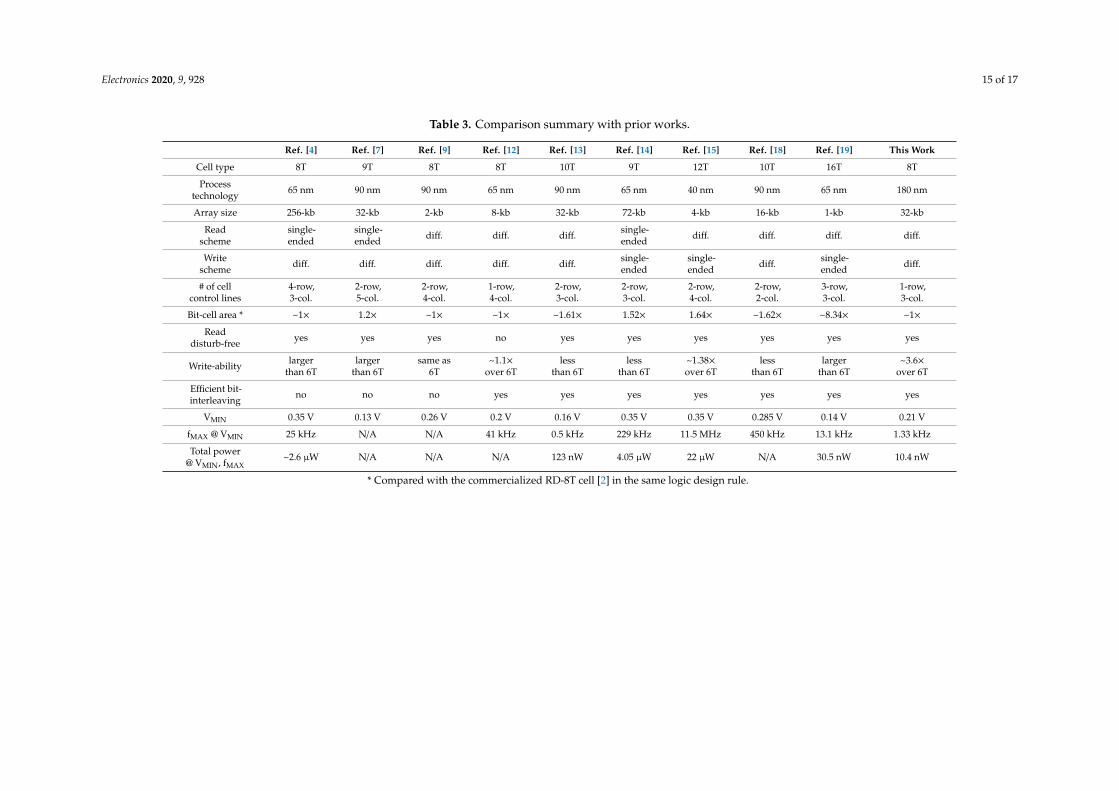
Electronics 2020, 9, 928 15 of 17
Table 3. Comparison summary with prior works.
Ref. [4] Ref. [7] Ref. [9] Ref. [12] Ref. [13] Ref. [14] Ref. [15] Ref. [18] Ref. [19] This Work
Cell type 8T 9T 8T 8T 10T 9T 12T 10T 16T 8T
Processtechnology 65 nm 90 nm 90 nm 65 nm 90 nm 65 nm 40 nm 90 nm 65 nm 180 nm
Array size 256-kb 32-kb 2-kb 8-kb 32-kb 72-kb 4-kb 16-kb 1-kb 32-kb
Readscheme
single-ended
single-ended diff. diff. diff. single-
ended diff. diff. diff. diff.
Writescheme diff. diff. diff. diff. diff. single-
endedsingle-ended diff. single-
ended diff.
# of cellcontrol lines
4-row,3-col.
2-row,5-col.
2-row,4-col.
1-row,4-col.
2-row,3-col.
2-row,3-col.
2-row,4-col.
2-row,2-col.
3-row,3-col.
1-row,3-col.
Bit-cell area * ~1× 1.2× ~1× ~1× ~1.61× 1.52× 1.64× ~1.62× ~8.34× ~1×
Readdisturb-free yes yes yes no yes yes yes yes yes yes
Write-ability largerthan 6T
largerthan 6T
same as6T
~1.1×over 6T
lessthan 6T
lessthan 6T
~1.38×over 6T
lessthan 6T
largerthan 6T
~3.6×over 6T
Efficient bit-interleaving no no no yes yes yes yes yes yes yes
VMIN 0.35 V 0.13 V 0.26 V 0.2 V 0.16 V 0.35 V 0.35 V 0.285 V 0.14 V 0.21 V
fMAX @ VMIN 25 kHz N/A N/A 41 kHz 0.5 kHz 229 kHz 11.5 MHz 450 kHz 13.1 kHz 1.33 kHz
Total power@ VMIN, fMAX
~2.6 µW N/A N/A N/A 123 nW 4.05 µW 22 µW N/A 30.5 nW 10.4 nW
* Compared with the commercialized RD-8T cell [2] in the same logic design rule.
Electronics 2020, 9, 928 16 of 17
Author Contributions: Y.C. proposed the idea and supervised the research. Y.C., T.K., and S.M. designed thecircuits. T.K. and S.M. performed the simulations and layouts. Y.C., T.K., and S.M. analyzed the data. T.K. wrotethe initial manuscript. Y.C. revised and finalized the paper. All authors have read and agreed to the publishedversion of the manuscript.
Funding: This research was funded by the Ministry of Education in Korea, grant numberNRF-2017R1D1A3B0 4028290.
Acknowledgments: This research was supported by Basic Science Research Program through the NationalResearch Foundation of Korea (NRF) funded by the Ministry of Education (2017R1D1A3B04028290). The authorsare thankful to the IC Design Education Center in Korea for the support of design software.
Conflicts of Interest: The authors declare no conflict of interest.
References
1. Calhoun, B.H.; Ryan, J.F.; Khanna, S.; Putic, M.; Lach, J. Flexible circuits and architectures for ultralow power.Proc. IEEE 2010, 98, 267–282. [CrossRef]
2. Chang, L.; Montoye, R.K.; Nakamura, Y.; Batson, K.A.; Eickemeyer, R.J.; Dennard, R.H.; Haensch, W.;Jamsek, D. An 8T-SRAM for variability tolerance and low-voltage operation in high-performance caches.IEEE J. Solid-State Circuits 2008, 43, 956–963. [CrossRef]
3. Calhoun, B.H.; Chandrakasan, A.P. A 256-kb 65-nm sub-threshold SRAM design for ultra-low-voltageoperation. IEEE J. Solid-State Circuits 2007, 42, 680–688. [CrossRef]
4. Verma, N.; Chandrakasan, A.P. A 256 kb 65 nm 8T subthreshold SRAM employing sense-amplifier redundancy.IEEE J. Solid-State Circuits 2008, 43, 141–149. [CrossRef]
5. Kim, T.-H.; Liu, J.; Keane, J.; Kim, C.H. A 0.2 V, 480 kb subthreshold SRAM with 1 k cells per bitline forultra-low-voltage computing. IEEE J. Solid-State Circuits 2008, 43, 518–529. [CrossRef]
6. Sinangil, M.E.; Verma, N.; Chandrakasan, A.P. A reconfigurable 8T ultra-dynamic voltage scalable (U-DVS)SRAM in 65 nm CMOS. IEEE J. Solid-State Circuits 2009, 44, 3163–3173. [CrossRef]
7. Chang, M.-F.; Chang, S.-W.; Chou, P.-W.; Wu, W.-C. A 130 mV SRAM with expanded write and read marginsfor subthreshold applications. IEEE J. Solid-State Circuits 2011, 46, 520–529. [CrossRef]
8. Kushwah, C.B.; Vishvakarma, S.K. A single-ended with dynamic feedback control 8T subthreshold SRAMcell. IEEE Trans. Very Large Scale Integr. Syst. 2016, 24, 373–377. [CrossRef]
9. Kulkarni, J.P.; Goel, A.; Ndai, P.; Roy, K. A read-disturb-free, differential sensing 1R/1W port, 8T bitcell array.IEEE Trans. Very Large Scale Integr. Syst. 2011, 19, 1727–1730. [CrossRef]
10. Do, A.-T.; Yeo, K.-S.; Kim, T.T.-H. A 32kb 9T SRAM with PVT-tracking read margin enhancement for ultra-lowvoltage operation. In Proceedings of the 2015 IEEE International Symposium on Circuits and Systems,Lisbon, Portugal, 24–27 May 2015; pp. 2553–2556.
11. Yabuuchi, M.; Nii, K.; Tsukamoto, Y.; Ohbayashi, S.; Nakase, Y.; Shinohara, H. A 45nm 0.6V cross-point8T SRAM with negative biased read/write assist. In Proceedings of the 2009 Symposium on VLSI Circuits,Kyoto, Japan, 16–18 June 2009; pp. 158–159.
12. Do, A.-T.; Low, J.Y.S.; Low, J.Y.L.; Kong, Z.-H.; Tan, X.; Yeo, K.-S. An 8T differential SRAM with improvednoise margin for bit-interleaving in 65 nm CMOS. IEEE Trans. Circuits Syst. I Regul. Pap. 2011, 58, 1252–1263.
13. Chang, I.J.; Kim, J.-J.; Park, S.P.; Roy, K. A 32 kb 10T sub-threshold SRAM array with bit-interleaving anddifferential read scheme in 90 nm CMOS. IEEE J. Solid-State Circuits 2009, 44, 650–658. [CrossRef]
14. Tu, M.-H.; Lin, J.-Y.; Tsai, M.-C.; Lu, C.-Y.; Lin, Y.-J.; Wang, M.-H.; Huang, H.-S.; Lee, K.-D.; Shih, W.-C.;Jou, S.-J.; et al. A single-ended disturb-free 9T subthreshold SRAM with cross-point data-aware writeword-line structure, negative bit-line, and adaptive read operation timing tracing. IEEE J. Solid-State Circuits2012, 47, 1469–1482. [CrossRef]
15. Chiu, Y.-W.; Hu, Y.-H.; Tu, M.-H.; Zhao, J.-K.; Chu, Y.-H.; Jou, S.-J.; Chuang, C.-T. 40 nm bit-interleaving 12Tsubthreshold SRAM with data-aware write-assist. IEEE Trans. Circuits Syst. I Regul. Pap. 2014, 61, 2578–2585.[CrossRef]
16. Lu, C.-Y.; Chuang, C.-T.; Jou, S.-J.; Tu, M.-H.; Wu, Y.-P.; Huang, C.-P.; Kan, P.-S.; Huang, H.-S.; Lee, K.-D.;Kao, Y.-S. A 0.325 V, 600-kHz, 40-nm 72-kb 9T subthreshold SRAM with aligned boosted write wordline andnegative write bitline write-assist. IEEE Trans. Very Large Scale Integr. Syst. 2015, 23, 958–962. [CrossRef]
17. Kulkarni, J.P.; Kim, K.; Roy, K. A 160 mV robust Schmitt trigger based subthreshold SRAM. IEEE J. Solid-StateCircuits 2007, 42, 2303–2313. [CrossRef]
Electronics 2020, 9, 928 17 of 17
18. Lo, C.-H.; Huang, S.-Y. P-P-N based 10T SRAM cell for low-leakage and resilient subthreshold operation.IEEE J. Solid-State Circuits 2011, 46, 695–704. [CrossRef]
19. Sarfraz, K.; He, J.; Chan, M. A 140-mV variation-tolerant deep sub-threshold SRAM in 65-nm CMOS. IEEE J.Solid-State Circuits 2017, 52, 2215–2220. [CrossRef]
20. Chung, Y.; Kim, H. A differential subthreshold SRAM cell for ultra-low voltage embedded computingapplications. Int. J. Appl. Eng. Res. 2017, 12, 7998–8003.
21. Pelliconi, R.; Iezzi, D.; Baroni, A.; Pasotti, M.; Rolandi, P.L. Power efficient charge pump in deep submicronstandard CMOS technology. IEEE J. Solid-State Circuits 2003, 38, 1068–1071. [CrossRef]
© 2020 by the authors. Licensee MDPI, Basel, Switzerland. This article is an open accessarticle distributed under the terms and conditions of the Creative Commons Attribution(CC BY) license (http://creativecommons.org/licenses/by/4.0/).