a novel design for highly compact low … · in this paper an area efficient design for highly...
TRANSCRIPT

International Journal of Advances in Engineering & Technology, Sept 2012.
©IJAET ISSN: 2231-1963
464 Vol. 4, Issue 2, pp. 464-473
A NOVEL DESIGN FOR HIGHLY COMPACT LOW POWER
AREA EFFICIENT 1-BIT FULL ADDERS
Shamima Khatoon
Department of Electronics & Communication Engg. Shri Ram Institute of Technology,
Jabalpur, Madhya- Pradesh, India
ABSTRACT
In this Paper an area efficient design for highly compact, low power 1-Bit Full adder is presented. The
proposed Full Adder is based on XNOR-XNOR hybrid CMOS design styles with 32nm and 120nm CMOS
process technologies. The XNOR gates used in the design are implemented using 3Mosfets only along with
proper W/L ratio among them. Reduced area is one of the most required features of the modern electronic
system designed for low cost and high yield, on the other hand, low power dissipation results in high
performance and portable applications. The tradeoff between cost and performance is fundamental to aim of
the proposed design. The implemented design consumes less than 1/6th
of the area as compared to other
existing Full adders with less delay and power dissipation without trading of driving capabilities and
reliabilities. The new Full adder successfully operates at low voltage upto 0.35V and operating frequency
range between 2MHz to 400MHz with excellent linearity, signal integrity and driving capability. The layout
designing is done manually using an educational tool called Micro wind 3.1.Simulation of layout and
parametric analysis is performed and results are discussed. It can be concluded that the proposed full adder
is more reliable in terms of Area, Power dissipation and Speed.
KEYWORDS: Area Efficient, Pass Transistor Logic(PTL), Transmission gate(TG), 3T( three transistors),
DSCH(Digital Schematic).
I. INTRODUCTION
Highly compact, Low power and fast circuits are the basic requirement of VLSI Designing. Increasing
demand of such circuits have fuelled much research into the different styles of VLSI design which can
be addressed at different design levels, such as the architectural, circuit, layout, and process
technology level. At the circuit design level, by means of proper choice of logic style and process
technology considerable effort can be made in the field of these areas. The absence of compact design
techniques leads to increased circuit cost because the die cost is a strong function of die area. High
power dissipation from a certain application can result in short battery life, while cooling and packing
them would be very difficult and thus leading to an unavoidable increase in the cost of the product.
The use more number of slow PMOS also reduces the speed. Conclusively, area efficiency as well as
energy efficiency both are significant.
So far several logic styles have been used to design full adders. One example of such design is the
standard static CMOS full adder [1]. The main drawback of static CMOS circuits is the existence of
the PMOS block, because of its low mobility compared to the NMOS devices. Therefore, PMOS
devices need to be seized up to attain the desired performance. Also in CMOS adders more number of
transistors are required to realize XOR-XNOR gates, resulting in complex design and increasing the
chip area. Energy efficient adders [7], [10] though have low PDP,but still consumes a significant area.
Another conventional adder is the complementary pass-transistor logic (CPL) [1]. Due to the presence
of lot of internal nodes and static inverters, there is large power dissipation. In the proposed adder
International Journal of Advances in Engineering & Technology, Sept 2012.
©IJAET ISSN: 2231-1963
465 Vol. 4, Issue 2, pp. 464-473
proper skewing and efficient utilization of NMOS and PMOS, along with proper choice of inputs,
PTL and TG can outperforms gate based design in terms of speed, accuracy and power dissipation. So
the high density layout, speed and compact design advantages of PTL and TG design style can be
utilized efficiently to design XNOR circuits and multiplexer circuits respectively with a conventional
CMOS style to design inverter circuit for proposed full adder. The proposed adder therefore can be
called as hybrid CMOS Full adder with a much reduced area, and thus the reduced circuit cost and
also can be called as Area Efficient Adder.
This Paper is structured as Follows: Section 2 introduce the related work regarding Full adders.
Section 3 briefly introduces the Proposed Hybrid Full Adder Design Methodology. Section 4
represents simulation tool and methodology. Section 5 represents Full Adder realization, i.e., the
layout designed in Microwind 3.1 version and their simulated waveforms. Section 6 shows the
simulation results. Section 7 includes the future work. Finally, Section 8 comprises of conclusion.
II. RELATED WORK REGARDING FULL ADDER OPTIMIZATION
Many Papers have been published regarding the optimization of Low power full adders, trying
different options for the Logic styles like standard CMOS logic[1], Centralized, XNOR/XNOR, and
XOR/XOR based hybrid logic style [7], [9,], [10], CMOS mixed mode logic family[18],Swing
restored CPL(SR-CPL)[11]. In the recent publication [7] logic structure for a full adder is prepared by
examining the full adder truth table, it can be seen that the Sum output is equal to the A⊕B value
when C=0 and it is equal to (A⊕ B)’ value when C=1. Thus, a multiplexer can be used to obtain the
respective value taking the C input as the selection signal. Following the same criteria, the Carry
output is equal to the A.B value when C=0 and it is equal to A+B value when C=1. Again, C can be
used to select the respective value for the required condition, driving a multiplexer. All these are
designed using hybrid logic structure which gives really complex structure.
The proposed adder design although uses Hybrid-CMOS logic design style [10] for the
implementation, but it generates the sum output with totally different concept. A PTL based 3
transistors XNOR gates are used to generate sum and a Pass Transistor based multiplexer to obtain
carry output. The proposed PTL directly XNOR the inputs by just using 3 MOSFETs only,
eliminating the used of inverters at the inputs, resulting in simple circuitry, reducing the size and
dissipation to large extent.
III. PROPOSED FULL ADDER DESIGN METHODOLOGY
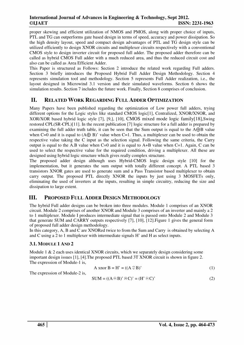
The hybrid Full adder designs can be broken into three modules. Module 1 comprises of an XNOR circuit. Module 2 comprises of another XNOR and Module 3 comprises of an inverter and mainly a 2 to 1 multiplexer. Module I produces intermediate signal that is passed onto Module 2 and Module 3 that generate SUM and CARRY outputs respectively [7], [10], [12].Figure 1 gives the general form of proposed full adder design methodology.
In this category, A, B and C are XNORed twice to from the Sum and Carry is obtained by selecting A
and C using a 2 to 1 multiplexer with intermediate signals H’ and H as select inputs.
3.1. MODULE 1 AND 2
Module 1 & 2 each uses identical XNOR circuits, which we separately design considering some
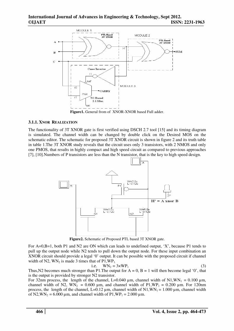
important design issues [1], [4].The proposed PTL based 3T XNOR circuit is shown in figure 2.
The expression of Module-1 is,
A xnor B = H’ = ((A⊕B)’ (1)
The expression of Module-2 is,
SUM = ((A⊕B)’⊕C)’ = (H’⊕C)’ (2)
International Journal of Advances in Engineering & Technology, Sept 2012.
©IJAET ISSN: 2231-1963
466 Vol. 4, Issue 2, pp. 464-473
Figure1. General from of XNOR-XNOR based Full adder.
3.1.1. XNOR REALIZATION
The functionality of 3T XNOR gate is first verified using DSCH 2.7 tool [15] and its timing diagram
is simulated. The channel width can be changed by double click on the Desired MOS on the
schematic editor. The schematic for proposed 3T XNOR circuit is shown in figure 2 and its truth table
in table 1.The 3T XNOR study reveals that the circuit uses only 3 transistors, with 2 NMOS and only
one PMOS, that results in highly compact and high speed circuit as compared to previous approaches
[7], [10].Numbers of P transistors are less than the N transistor, that is the key to high speed design.
Figure2. Schematic of Proposed PTL based 3T XNOR gate.
For A=0,B=1, both P1 and N2 are ON which can leads to undefined output, ‘X’, because P1 tends to
pull up the output node while N2 tends to pull down the output node. For these input combination an
XNOR circuit should provide a legal ‘0’ output. It can be possible with the proposed circuit if channel
width of N2, WN2 is made 3 times that of P1,WP1.
i.e. WN2 = 3×WP1 (3) Thus,N2 becomes much stronger than P1.The output for A = 0, B = 1 will then become legal ‘0’, that is the output is provided by stronger N2 transistor.
For 32nm process, the length of the channel, L=0.040 µm, channel width of N1,WN1 = 0.100 µm, channel width of N2, WN2 = 0.600 µm, and channel width of P1,WP1 = 0.200 µm. For 120nm process, the length of the channel, L=0.12 µm, channel width of N1,WN1 = 1.000 µm, channel width of N2,WN2 = 6.000 µm, and channel width of P1,WP1 = 2.000 µm.
International Journal of Advances in Engineering & Technology, Sept 2012.
©IJAET ISSN: 2231-1963
467 Vol. 4, Issue 2, pp. 464-473
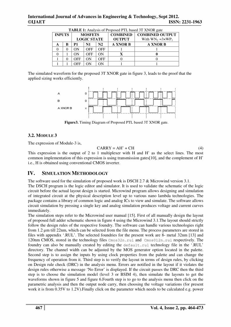
TABLE 1: Analysis of Proposed PTL based 3T XNOR gate
INPUTS MOSFETS
LOGIC STATE
COMBINED
OUTPUT
COMBINED OUTPUT
With WN2 =3×WP1
A B P1 N1 N2 A XNOR B A XNOR B
0 0 ON OFF OFF 1 1
0 1 ON OFF ON X 0
1 0 OFF ON OFF 0 0
1 1 OFF ON ON 1 1
The simulated waveform for the proposed 3T XNOR gate in figure 3, leads to the proof that the
applied sizing works efficiently.
Figure3. Timing Diagram of Proposed PTL based 3T XNOR gate.
3.2. MODULE 3
The expression of Module-3 is,
CARRY = AH’ + CH (4)
This expression is the output of 2 to 1 multiplexer with H and H’ as the select lines. The most
common implementation of this expression is using transmission gates[10], and the complement of H’
i.e., H is obtained using conventional CMOS inverter.
IV. SIMULATION METHODOLOGY
The software used for the simulation of proposed work is DSCH 2.7 & Microwind version 3.1.
The DSCH program is the logic editor and simulator. It is used to validate the schematic of the logic
circuit before the actual layout design is started. Microwind program allows designing and simulation
of integrated circuit at the physical description level up to various nano lambda technologies. The
package contains a library of common logic and analog ICs to view and simulate. The software allows
circuit simulation by pressing a single key and analog simulation produces voltage and current curves
immediately.
The simulation steps refer to the Microwind user manual [15]. First of all manually design the layout
of proposed full adder schematic shown in figure 4 using the Microwind 3.1.The layout should strictly
follow the design rules of the respective foundry. The software can handle various technologies right
from 1.2 µm till 22nm, which can be selected from the file menu. The process parameters are stored in
files with appendix ‘.RUL’. The selected foundries for the present work are 8- metal 32nm [13] and
120nm CMOS, stored in the technology files Cmos32n.rul and Cmos012n.rul respectively. The
foundry can also be manually created by editing the default.rul technology file in the ‘.RUL’
directory. The channel width can be adjusted by the MOS generator option located in the palette.
Second step is to assign the inputs by using clock properties from the palette and can change the
frequency of operation from it. Third step is to verify the layout in terms of design rules, by clicking
on Design rule check (DRC) in the analysis menu. Errors are notified in the layout if it violates the
design rules otherwise a message ‘No Error’ is displayed. If the circuit passes the DRC then the third
step is to choose the simulation model (level 3 or BSIM 4), then simulate the layouts to get the
waveforms shown in figure 5 and figure 6.Fourth step is to go to the analysis menu then click on the
parametric analysis and then the output node carry, then choosing the voltage variations (for present
work it is from 0.35V to 1.2V).Finally click on the parameter which needs to be calculated e.g. power
International Journal of Advances in Engineering & Technology, Sept 2012.
©IJAET ISSN: 2231-1963
468 Vol. 4, Issue 2, pp. 464-473
dissipation(mw),maximum current Idd (ma),rise time, tr(ns), and fall time, tf (ns) from A to carry, for
chosen model and get the results as shown in figure7 and 8.
The command File -> Properties provides some information about the current technology, the
percentage of memory used by the layout and the size of the layout plus its detailed contents.
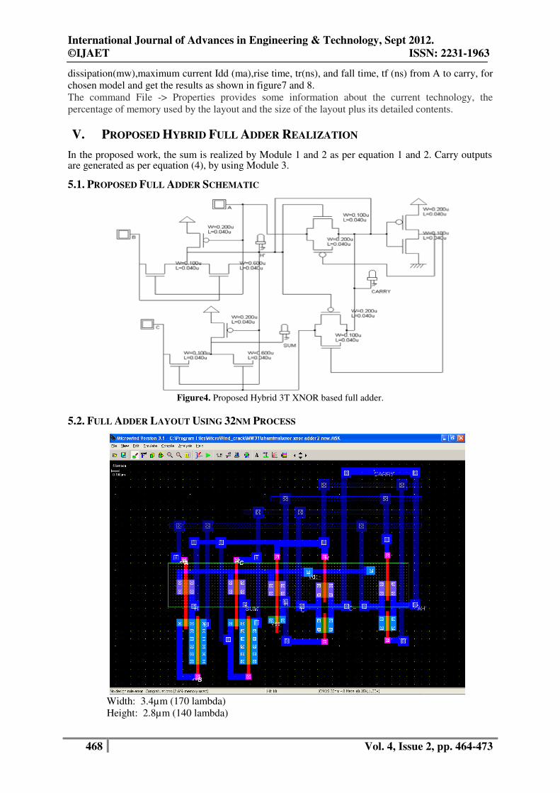
V. PROPOSED HYBRID FULL ADDER REALIZATION In the proposed work, the sum is realized by Module 1 and 2 as per equation 1 and 2. Carry outputs are generated as per equation (4), by using Module 3.
5.1. PROPOSED FULL ADDER SCHEMATIC
Figure4. Proposed Hybrid 3T XNOR based full adder.
5.2. FULL ADDER LAYOUT USING 32NM PROCESS
Width: 3.4µm (170 lambda)
Height: 2.8µm (140 lambda)

International Journal of Advances in Engineering & Technology, Sept 2012.
©IJAET ISSN: 2231-1963
469 Vol. 4, Issue 2, pp. 464-473
Surf: 9.5µm2
5.3. FULL ADDER SIMULATED WAVEFORM USING 32NM PROCESS
Figure 5.Xnor-Xnor based Full adder waveform,32n
5.4. FULL ADDER LAYOUT USING 120NM PROCESS
Width: 12.4µm (206 lambda)
Height: 8.4µm (140 lambda)
Surf: 103.8µm2
5.5. FULL ADDER SIMULATED WAVEFORM 120NM

International Journal of Advances in Engineering & Technology, Sept 2012.
©IJAET ISSN: 2231-1963
470 Vol. 4, Issue 2, pp. 464-473
Figure 6.Xnor-Xnor based Full adder waveform 120nm
VI. SIMULATION RESULTS
The Performance of the circuit is evaluated based on their Area, Power dissipation, and Speed.
All the simulations are performed using Microwind 3.1[15].All the results are measured using the
MOS Empherical level 3 and BSIM Model 4 having different supply voltages like 0.35V, 0.60V,
0.80V, 1.20V and the operating Temperature is 27°C. In the Empherical Level 3 the threshold
voltage is 0.4V, Gate oxide thickness 3nm and Lateral diffusion into channel is 0.01µm.In the BSIM
Model 4 the threshold voltage is 0.18V, Gate oxide thickness 1.5 nm.
Figure 7(a) shows the power dissipation for 32nm technology using model 3 and figure 7(b) using
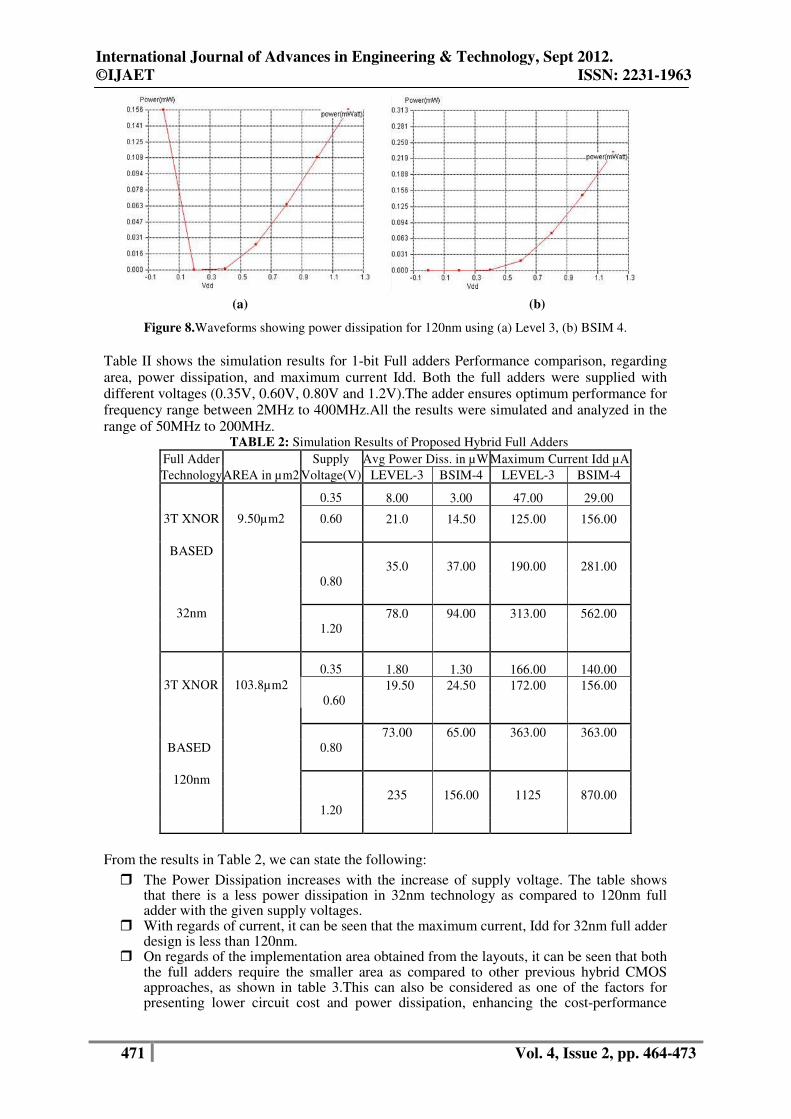
BSIM4.Similarly, figure 8(a) shows the power dissipation for 120nm foundry using model 3 and
figure 8(b) using BSIM4.
(a) (b)
Figure 7.Waveforms showing power dissipation for 32nm Full Adder using (a) Level 3, (b) BSIM4.
International Journal of Advances in Engineering & Technology, Sept 2012.
©IJAET ISSN: 2231-1963
471 Vol. 4, Issue 2, pp. 464-473
(a) (b)
Figure 8.Waveforms showing power dissipation for 120nm using (a) Level 3, (b) BSIM 4.
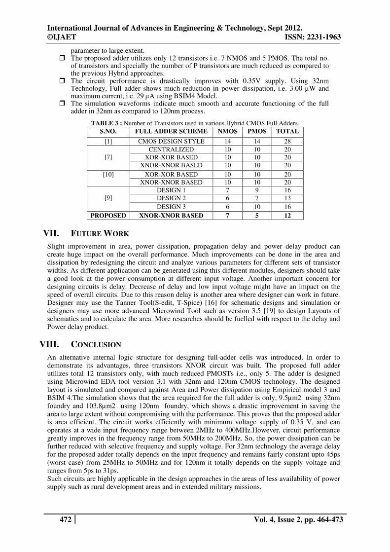
Table II shows the simulation results for 1-bit Full adders Performance comparison, regarding area, power dissipation, and maximum current Idd. Both the full adders were supplied with different voltages (0.35V, 0.60V, 0.80V and 1.2V).The adder ensures optimum performance for frequency range between 2MHz to 400MHz.All the results were simulated and analyzed in the range of 50MHz to 200MHz.
TABLE 2: Simulation Results of Proposed Hybrid Full Adders Full Adder Supply Avg Power Diss. in µW Maximum Current Idd µA
TechnologyAREA in µm2 Voltage(V) LEVEL-3 BSIM-4 LEVEL-3 BSIM-4
0.35 8.00 3.00 47.00 29.00
3T XNOR 9.50µm2 0.60 21.0 14.50 125.00 156.00
BASED
0.80 35.0 37.00 190.00 281.00
32nm
1.20 78.0 94.00 313.00 562.00
0.35 1.80 1.30 166.00 140.00
3T XNOR 103.8µm2
0.60 19.50 24.50 172.00 156.00
BASED
0.80
73.00 65.00 363.00 363.00
120nm
1.20
235 156.00 1125 870.00
From the results in Table 2, we can state the following:
� The Power Dissipation increases with the increase of supply voltage. The table shows
that there is a less power dissipation in 32nm technology as compared to 120nm full adder with the given supply voltages.
� With regards of current, it can be seen that the maximum current, Idd for 32nm full adder design is less than 120nm.
� On regards of the implementation area obtained from the layouts, it can be seen that both the full adders require the smaller area as compared to other previous hybrid CMOS approaches, as shown in table 3.This can also be considered as one of the factors for presenting lower circuit cost and power dissipation, enhancing the cost-performance
International Journal of Advances in Engineering & Technology, Sept 2012.
©IJAET ISSN: 2231-1963
472 Vol. 4, Issue 2, pp. 464-473
parameter to large extent. � The proposed adder utilizes only 12 transistors i.e. 7 NMOS and 5 PMOS. The total no.
of transistors and specially the number of P transistors are much reduced as compared to the previous Hybrid approaches.
� The circuit performance is drastically improves with 0.35V supply. Using 32nm Technology, Full adder shows much reduction in power dissipation, i.e. 3.00 µW and maximum current, i.e. 29 µA using BSIM4 Model.
� The simulation waveforms indicate much smooth and accurate functioning of the full adder in 32nm as compared to 120nm process.
TABLE 3 : Number of Transistors used in various Hybrid CMOS Full Adders.
S.NO. FULL ADDER SCHEME NMOS PMOS TOTAL
[1] CMOS DESIGN STYLE 14 14 28
[7]
CENTRALIZED 10 10 20
XOR-XOR BASED 10 10 20
XNOR-XNOR BASED 10 10 20
[10] XOR-XOR BASED 10 10 20
XNOR-XNOR BASED 10 10 20
[9]
DESIGN 1 7 9 16
DESIGN 2 6 7 13
DESIGN 3 6 10 16
PROPOSED XNOR-XNOR BASED 7 5 12
VII. FUTURE WORK
Slight improvement in area, power dissipation, propagation delay and power delay product can create huge impact on the overall performance. Much improvements can be done in the area and dissipation by redesigning the circuit and analyze various parameters for different sets of transistor widths. As different application can be generated using this different modules, designers should take a good look at the power consumption at different input voltage. Another important concern for designing circuits is delay. Decrease of delay and low input voltage might have an impact on the speed of overall circuits. Due to this reason delay is another area where designer can work in future. Designer may use the Tanner Tool(S-edit, T-Spice) [16] for schematic designs and simulation or designers may use more advanced Microwind Tool such as version 3.5 [19] to design Layouts of schematics and to calculate the area. More researches should be fuelled with respect to the delay and Power delay product.
VIII. CONCLUSION
An alternative internal logic structure for designing full-adder cells was introduced. In order to demonstrate its advantages, three transistors XNOR circuit was built. The proposed full adder utilizes total 12 transistors only, with much reduced PMOSTs i.e., only 5. The adder is designed using Microwind EDA tool version 3.1 with 32nm and 120nm CMOS technology. The designed layout is simulated and compared against Area and Power dissipation using Empirical model 3 and BSIM 4.The simulation shows that the area required for the full adder is only, 9.5µm2 using 32nm foundry and 103.8µm2 using 120nm foundry, which shows a drastic improvement in saving the area to large extent without compromising with the performance. This proves that the proposed adder is area efficient. The circuit works efficiently with minimum voltage supply of 0.35 V, and can operates at a wide input frequency range between 2MHz to 400MHz.However, circuit performance greatly improves in the frequency range from 50MHz to 200MHz. So, the power dissipation can be further reduced with selective frequency and supply voltage. For 32nm technology the average delay for the proposed adder totally depends on the input frequency and remains fairly constant upto 45ps (worst case) from 25MHz to 50MHz and for 120nm it totally depends on the supply voltage and ranges from 5ps to 31ps. Such circuits are highly applicable in the design approaches in the areas of less availability of power supply such as rural development areas and in extended military missions.
International Journal of Advances in Engineering & Technology, Sept 2012.
©IJAET ISSN: 2231-1963
473 Vol. 4, Issue 2, pp. 464-473
ACKNOWLEDGEMENTS
The Authors acknowledge the support of the Shri Ram Institute of Technology, Jabalpur, M.P.
(INDIA).She also like to specially thank Prof. Ravi Mohan, HOD (M-TECH),and Prof. Summit
Sharma, HOD(B.E) to help her from their valuable guidance.
REFERENCES
[1] N. Weste and K. Eshraghian, (2002) Principles of CMOS VLSI Design: A System Perspective Reading,
Pearson Education, Addison –Wesley.
[2] John P. Uyemura, (2002) Introduction to VLSI circuits and systems, Wiley John & Sons, Inc.
[3] Sung-Mo Kang, Yusuf Leblebici, (2003) CMOS Digital Integrated Circuits: Analysis and Design, TATA
Mc GRAW-HILL.
[4] N. Weste and D. Harris, (2005) CMOS VLSI Design, Pearson Wesley.
[5] J. Uyemura, (1999) CMOS Logic Circuit Design, Kluwer.
[6] N. Jha and S. Gupta, (2003) Testing of Digital Systems. Cambridge, U.K.
[7] Candy Goyal, Ashish Kumar, “Comparative Analysis of Energy Efficient Low Power 1bit Full Addera
at 120 nm technology”, IJAET July-2012 ISSN 2231-1963 Vol. 3, Issue 1, pp. 501-509.
[8] Rajkumar Sarma and Veerati Raju, “Design And Performance Analysis Of Hybrid Adders For High
Speed Arithmetic Circuit” International Journal of VLSI design & Communication Systems (VLSICS)
Vol.3, No.3, June 2012 DOI : 10.5121/vlsic.2012.3303 21
[9] Subodh Wairya, Rajendra Kumar Nagaria,and Sudarshan Tiwari, “Comparative Performance Analysis of
XORXNOR Function Based High-Speed CMOS Full Adder Circuits For Low Voltage”,VLSI Design
International Journal of VLSI design & Communication Systems (VLSICS) Vol.3, No.2, April 2012
[10] Mohammad Shamim Imtiaz, Md Abdul Aziz Suzon, Mahmudur Rahman, “Design of Energy-Efficient
Full Adders Using Hybrid-CMOS Logic Style” IJAET Jan-2012 ISSN 2231-1963 Vol. 2, Issue 1, pp. 190-
202.
[11] Mariano Aguirre-Hernandez and Monico Linares-Aranda, “CMOS Full-Adders for Energy-Efficient
Arithmetic Applications” IEEE Transactions on Very Large Scale Integration (VLSI) Systems, APRIL 2011
VOL. 19, NO. 4. [12] S. Wariya, Himanshu Pandey, R.K.Nagaria and S. Tiwari,(2010)“Ultra low voltage high speed 1bit adder,” IEEE Trans. Very Large Scale Integeration.
[13] Etienne SICARD,Syed Mahfuzul Aziz, (2010)“Introducing 32 nm technology in Microwind31” Microwind Application Note 32 Nm Technology.
[14] Nilesh P. Bobade, Rajashree H. Umbarkar, Priyanka U. Badhe,Shruti V. Kohale, (2012) ”Design
performance of CMOS Circuits in Microwind”,IJCA. [15] Microwind and DSCH version 3.1, User’s Manual, Copyright 1997-2007, Microwind INSA France.
[16] Tanner EDA Inc. 1988, User’s Manual, 2005.
[17] Mojtabavi Naeini Mahshid and Navi Keivan, (2010) “A New Full-Adder Based on Majority Function
and Standard Gates”, Journal of Communication and Computer, Vol. 7, No. 5 pp. 1-7.
[18] Subodh Wairya, Rajendra Kumar Nagaria, Sudarshan Tiwari “New design methodologies for High-
speed mixed-mode Cmos Full adder circuits” International Journal of VLSI design & Communication
Systems (VLSICS) Vol.2, No.2, June 2011 DOI : 10.5121/vlsic.2011.2207 78
[19] Microwind and DSCH version 3.5, User’s Manual, Copyright 1997-2010,Microwind INSA Toulouse,
University of Toulouse France.
AUTHOR
Shamima Khatoon received her B.E.(hons) from Shri Ram Institute of Technology,
Jabalpur, M.P. in Electronics and Communication Engg and pursuing her M.Tech in
VLSI DESIGN from Shri Ram Institute of Technology, Jabalpur, M.P. She is in 4th
Semester and engaged in completing her dissertation part 2 for the M-TECH thesis. Her
research interests include Low Power and area efficient VLSI Design, VLSI design
softwares such as Microwind versions 3,3.1,3.5 & DSCH versions 2.7,3,3.1,3.5, RFID
technology, Self-powered microelectronics systems.