a novel self-reference sensing scheme for mlc...
TRANSCRIPT

A NOVEL SELF-REFERENCE SENSING SCHEME
FOR MLC MRAM
by
Zheng Li
B.S. in Electric and Information, Beihang University, Beijing,
China, 2014
Submitted to the Graduate Faculty of
Swanson School of Engineering in partial fulfillment
of the requirements for the degree of
Master of Science
University of Pittsburgh
2017

UNIVERSITY OF PITTSBURGH
SWANSON SCHOOL OF ENGINEERING
This thesis was presented
by
Zheng Li
It was defended on
November 11, 2016
and approved by
Hai Li, Ph.D., Associate Professor, Department of Electrical and Computer Engineering
Yiran Chen, Ph.D., Associate Professor, Department of Electrical and Computer
Engineering
Samuel J Dickerson, Ph.D., Assistance Professor,Department of Electrical and Computer
Engineering
Thesis Advisor: Hai Li, Ph.D., Associate Professor, Department of Electrical and
Computer Engineering
ii

Copyright c⃝ by Zheng Li
2017
iii

A NOVEL SELF-REFERENCE SENSING SCHEME FOR MLC MRAM
Zheng Li, M.S.
University of Pittsburgh, 2017
Magnetic random access memory (MRAM) is a promising nonvolatile memory technology
targeted on on-chip or embedded applications. Storage density is one of the major design
concerns of MRAM. In recent years, many researches have been performed to improve the
storage density and enhance the scalability of MRAM, such as shrinking the size and switch-
ing energy of magnetic tunneling junction (MTJ) devices. Recently, a tri-bit cell (TBC)
structure was proposed to enlarge the storage density of MRAM. The typical sensing scheme
for TBC sensing is suffering from large sensing latency and limited margin. In this work,
a new self-reference sensing scheme for the TBC MRAM cell was proposed based on its
unique property referred as resistance levels ordering. Simulation results show that com-
pared to conventional design, the proposed self-reference scheme achieves on average 61%
saving on sensing latency while also demonstrating significantly enhanced tolerance to device
parametric variations.
Keywords: Non-volatile Memory, MRAM, MTJ, Sensing Circuit.
iv
TABLE OF CONTENTS
PREFACE . . . . . . . . . . . . . . . . . . . . . . . . . . . . . . . . . . . . . . . . . x
1.0 INTRODUCTION . . . . . . . . . . . . . . . . . . . . . . . . . . . . . . . . . 1
1.1 Motivations . . . . . . . . . . . . . . . . . . . . . . . . . . . . . . . . . . . . 1
1.2 Objectives . . . . . . . . . . . . . . . . . . . . . . . . . . . . . . . . . . . . . 2
1.3 Thesis Outline . . . . . . . . . . . . . . . . . . . . . . . . . . . . . . . . . . 3
2.0 PRELIMINARIES . . . . . . . . . . . . . . . . . . . . . . . . . . . . . . . . . 4
2.1 MTJ Basics . . . . . . . . . . . . . . . . . . . . . . . . . . . . . . . . . . . . 4
2.1.1 Field Induced MTJ Basics . . . . . . . . . . . . . . . . . . . . . . . . 4
2.1.2 TAS-MTJ Basics . . . . . . . . . . . . . . . . . . . . . . . . . . . . . . 6
2.1.3 STT-MTJ Basics . . . . . . . . . . . . . . . . . . . . . . . . . . . . . 7
2.2 MRAM Cell Design . . . . . . . . . . . . . . . . . . . . . . . . . . . . . . . 8
2.2.1 FIMS-and TAS-MRAM Cell . . . . . . . . . . . . . . . . . . . . . . . 8
2.2.2 STT-MRAM Cell . . . . . . . . . . . . . . . . . . . . . . . . . . . . . 9
2.3 MLC Design for MRAM . . . . . . . . . . . . . . . . . . . . . . . . . . . . . 10
2.3.1 STT-MLC-MRAM Design . . . . . . . . . . . . . . . . . . . . . . . . 10
2.3.2 TAS-MLC-MRAM Design . . . . . . . . . . . . . . . . . . . . . . . . 11
3.0 SENSING SCHEME EXPLORATION FOR MLC MRAM . . . . . . . 14
3.1 Conventional Sensing Scheme . . . . . . . . . . . . . . . . . . . . . . . . . . 14
3.2 Typical Self Referencing Sensing Scheme . . . . . . . . . . . . . . . . . . . . 15
3.3 Three Step Sensing Scheme . . . . . . . . . . . . . . . . . . . . . . . . . . . 16
4.0 SENSING CIRCUIT DESIGN FOR TLC MRAM SENSING . . . . . . 20
4.1 Sense Amplifier Design . . . . . . . . . . . . . . . . . . . . . . . . . . . . . . 20
v

4.2 TSSRS Circuitry Design . . . . . . . . . . . . . . . . . . . . . . . . . . . . . 21
5.0 SIMULATION AND SENSING PERFORMANCE ANALYSIS . . . . 23
5.1 TSSRS Scheme Functional Simulation . . . . . . . . . . . . . . . . . . . . . 24
5.2 Impacts of Process Variation on TSSRS Scheme . . . . . . . . . . . . . . . . 26
5.3 Thermal Dependency in Reading operation . . . . . . . . . . . . . . . . . . 27
6.0 CONCLUSION . . . . . . . . . . . . . . . . . . . . . . . . . . . . . . . . . . . 29
BIBLIOGRAPHY . . . . . . . . . . . . . . . . . . . . . . . . . . . . . . . . . . . . 30
vi
LIST OF TABLES
1 States Truth Table . . . . . . . . . . . . . . . . . . . . . . . . . . . . . . . . . 17
2 Variables and Parameters . . . . . . . . . . . . . . . . . . . . . . . . . . . . . 23
vii

LIST OF FIGURES
1 (a) Three-layer structure of MTJ; (b) Switching between low resistance RP
(parallel) and high resistance RAP (anti-parallel). . . . . . . . . . . . . . . . . 5
2 FIMS-MTJ: (a) structure and (b) switching. . . . . . . . . . . . . . . . . . . 6
3 TAS-MTJ stacked structure. . . . . . . . . . . . . . . . . . . . . . . . . . . . 7
4 (a) STT-MTJ stacked structure; (b) Illustration of static I-R curve of STT-MTJ. 8
5 Typical FIMS-MRAM cell design. . . . . . . . . . . . . . . . . . . . . . . . . 9
6 1T1J STT-MTAM cell structure, 4X4 array. . . . . . . . . . . . . . . . . . . . 10
7 STT-MLC-MTJ design: (a) Parallel MLC configuration; (b) Series MLC con-
figuration. . . . . . . . . . . . . . . . . . . . . . . . . . . . . . . . . . . . . . 11
8 (a) TAS-MLC-MTJ structure; (b) Relationship between magnetization angles
and resistance levels. . . . . . . . . . . . . . . . . . . . . . . . . . . . . . . . . 12
9 (a) Sketch of typical read scheme; (b) Schematic of the conventional read circuit
for STT-MRAM. . . . . . . . . . . . . . . . . . . . . . . . . . . . . . . . . . . 15
10 (a) Sensing Direction for three steps; (b) Processing Flow depicting the pro-
posed sensing methodology. . . . . . . . . . . . . . . . . . . . . . . . . . . . . 18
11 (a) Schematic of SA; (b) Layout of SA. . . . . . . . . . . . . . . . . . . . . . 20
12 Transient response of SA. . . . . . . . . . . . . . . . . . . . . . . . . . . . . . 21
13 Schematic of the proposed scheme. . . . . . . . . . . . . . . . . . . . . . . . . 22
14 The transient response of TSSRS scheme: (a) Three steps sensing “#5”;
(b)Two comparisons of “#7”; (c) Two comparisons of “#2”. . . . . . . . . . 25
viii
15 The sensing voltage distributions of (a) the conventional MLC STT-MRAM
and (b) TBC MRAM. Note that TBC MRAM has only 5 distinct resistance
states; (c) The error rate vs. the standard deviation of key parameters. . . . . 27
16 Temperature-dependent sensing margin. . . . . . . . . . . . . . . . . . . . . . 28
ix

PREFACE
At the beginning of this thesis, I would like to thank all those people who made my thesis
possible and unforgettable.
I wish to express my sincere gratitude to my supervisor, Prof. Hai Li, for her guidance
and support throughout my study of the Swanson School of Engineering at the University
of Pittsburgh. Her extensive insight and devotion into research has kept me motivated.
She gave me the precious opportunity to join in Evolutionary Intelligence lab which had
enormous significance to me. I would also thank my co-advisor in EI-Lab, Dr. Yiran Chen,
for his support, assistance and valuable points.
Also, I would extend my sincere thanks to Dr. Samuel J Dickerson, for his charming
personality and professional dedication. He teaches me a lot, from the aspects of both
academy and engineering.
I am also indebted to my friends and team members in EI-Lab. Without their passionate
assistance, the thesis would not have finished.
Finally, I would give my profound gratitude to my parents for providing me with support
and encouragement throughout my years of study. This work would not have been finished
possibly without them.
x

1.0 INTRODUCTION
1.1 MOTIVATIONS
The demands for high capacity and high speed nonvolatile memory dramatically increase
due to the fast growth of the computing capability. Nevertheless, Complementary metalox-
idesemiconductor (CMOS) based Dynamic Random Access Memory (DRAM) and Static
Random Access Memory (SRAM) suffers from dominant leakage power issue and Flash
memory (NAND and NOR) faces significant scaling challenges at 32nm technology node
and beyond [1, 2].
Magnetic random access memory (MRAM) have received considerable attentions in last
decade as a promising candidate to replace DRAM and SRAM. Many attractive properties
of MRAM have been demonstrated, such as non-volatility, nanosecond access delay, COMS-
compatibility, high integration density and good scalability [3, 4, 5].
In an MRAM cell, data is stored as the two or more resistance states of a magnetic
tunneling junction (MTJ) device. The resistance states of the MTJ is determined by the
magnetization of the magnetic layers. There are several switching schemes for MRAM pro-
gramming. 1) The typical scheme is Field Induced Magnetic Switching, MTJ is switched
by applying magnetic field energized by current in a single line or a pair of lines[toggle etc].
Commercialized MRAM chips based on ”Toggle-Switching” has been shipped by Freescale
Semiconductor at 2005 [6]. Energy consuming and scalability issues due to high driving
current remain as a bottleneck for MRAM scaling down. 2) Spin Transfer Torque Mag-
netic Random Access Memory (STT-MRAM) [7, 8] is another promising technology whose
switching is achieved by injecting bi-directional current. 3) Thermally-assisted Switching
MRAM (TAS-MRAM) [9, 10] is emerged as another next generation technology exploiting
1
the temperature dependence of ferromagnet/antiferromagnet interfacial exchange coupling
to overcome the write consumption versus thermal stability dilemma usually observed in
magnetic recording technologies.
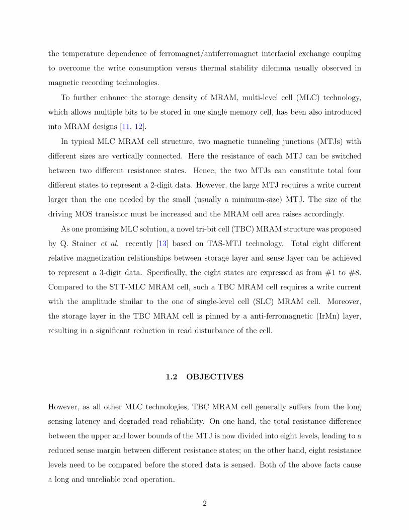
To further enhance the storage density of MRAM, multi-level cell (MLC) technology,
which allows multiple bits to be stored in one single memory cell, has been also introduced
into MRAM designs [11, 12].
In typical MLC MRAM cell structure, two magnetic tunneling junctions (MTJs) with
different sizes are vertically connected. Here the resistance of each MTJ can be switched
between two different resistance states. Hence, the two MTJs can constitute total four
different states to represent a 2-digit data. However, the large MTJ requires a write current
larger than the one needed by the small (usually a minimum-size) MTJ. The size of the
driving MOS transistor must be increased and the MRAM cell area raises accordingly.
As one promising MLC solution, a novel tri-bit cell (TBC) MRAM structure was proposed
by Q. Stainer et al. recently [13] based on TAS-MTJ technology. Total eight different
relative magnetization relationships between storage layer and sense layer can be achieved
to represent a 3-digit data. Specifically, the eight states are expressed as from #1 to #8.
Compared to the STT-MLC MRAM cell, such a TBC MRAM cell requires a write current
with the amplitude similar to the one of single-level cell (SLC) MRAM cell. Moreover,
the storage layer in the TBC MRAM cell is pinned by a anti-ferromagnetic (IrMn) layer,
resulting in a significant reduction in read disturbance of the cell.
1.2 OBJECTIVES
However, as all other MLC technologies, TBC MRAM cell generally suffers from the long
sensing latency and degraded read reliability. On one hand, the total resistance difference
between the upper and lower bounds of the MTJ is now divided into eight levels, leading to a
reduced sense margin between different resistance states; on the other hand, eight resistance
levels need to be compared before the stored data is sensed. Both of the above facts cause
a long and unreliable read operation.
2
In this work, a new three-step self-reference sensing scheme was proposed to improve the
read performance of the TBC MRAM cell.
By leveraging a unique observation of TBC MRAM cell called state ordering, the re-
sistance state of the cell can be sensed by using the state orders instead of the absolute
resistance values. Also, statistical analysis shows that this scheme can significantly improve
the read reliability of TBC MRAM cell when device parametric variations are taken into
account, paving a path toward continuous MRAM technology scaling.
1.3 THESIS OUTLINE
The rest of this work is organized as follows: Chapter II gives preliminary of TBC MRAM
cell, including MTJ switching schemes and typical MLC designs; Chapter III illustrates the
proposed three-step self-reference sensing scheme based on TAS-MTJ; Chapter IV presents
the simulation results by considering the device parametric variations; and Chapter V con-
cludes this work.
3

2.0 PRELIMINARIES
2.1 MTJ BASICS
2.1.1 Field Induced MTJ Basics
The MTJ is a three-layer stacked structure which includes two ferromagnetic layers (CoFeB,
typically) and one oxide barrier layer, e.g., MgO and AlO [14]. MTJ can be regarded as a
three-layer structure as shown in Fig. 1(a). The free layer, oxide layer and fixed layer, or
known as reference layer. As the name implies, the magnetization direction of free layer is
switchable while that of fixed layer is fixed. Relations between magnetizations of free layer
and fixed layer determines the resistance of the MTJ device. And the data was stored as
the resistance of MTJ. For example, when the magnetic direction of the two layers are in
the same direction. MTJ will show a low resistance, it means 0. when magnetization of two
layers are in the opposite direction, MTJ will be in high resistance, it means 1, as shown in
Fig. 1(b).
4

Figure 1: (a) Three-layer structure of MTJ; (b) Switching between low resistance RP (par-
allel) and high resistance RAP (anti-parallel).
There are several advanced technics to change the magnetic direction of free layer with
lower power consumption and higher programming reliability as introduced previously: FIMS
MTJ, TAS MTJ and STT MTJ.
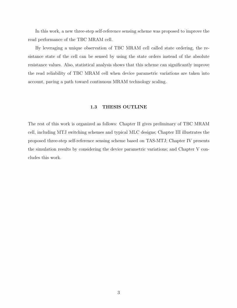
Fig. 2(a) illustrates the structure of FIMS-MTJ. The FIMS-MTJ can be switched by a
magnetic field generated by two current lines close to the MTJ (Toggle MRAM [6]). The
field applied on the free layer is the vector sum of fields generated by two write lines. It is
strong enough to switch the free layer while the single write field is not sufficiently large to
switch the free layer. It can help to solve the half selected issue in FIMS-MRAM, as shown
in Fig. 2(b).
It should also be noted that if only a single line current is applied (half-selected bits),
the 45 field angle with 1/√2 cannot switch the state. In fact, the single-line field raises the
switching energy barrier of those bits, so that they are stabilized against reversal during the
field pulse. Toggle MRAM using pulses with different phases was proposed to help improve
bit selectivity in an array.
5
Figure 2: FIMS-MTJ: (a) structure and (b) switching.
2.1.2 TAS-MTJ Basics
Actually the current can be in order of few milli-ampere in FIMS-MTJ. Therefore, the writing
power consumption is relatively high. Consequently, TAS and STT switching scheme was
proposed to reduce the writing power consumption.
In the case of TAS-MRAM shown in Fig. 3, From top to bottom, the first two layers
construct a storage layer, including a ferromagnetic layer (CoFeB) and an anti-ferromagnetic
layer (IrMn) which is used to pin the magnetization of the CoFeB layer. The layer at the
bottom, which is also a ferromagnetic layer, is called sense layer. An isolate barrier layer
(MgO) is inserted between the storage layer and the sense layer to separate them. As can
be noticed, the TAS-MTJ nano-pillar is slightly modified compared with FIMS-MTJ by
pinning the storage layers magnetization with an anti-ferromagnet(for example, IrMn [9]) by
the exchange bias coupling occurring at their interface. To switch MTJ, heating current (Ih)
is passed through the MTJ stack to heat the junction above the blocking temperature of the
6
free layer. When heated above the antiferromagnets blocking temperature, the ferromagnetic
layer (storage layer) becomes free to switch, and its magnetization can be set by a magnetic
field. Typically, the heating current is around several milli-ampere [15]. Afterwards, the
heating is stopped, the junction cools down below the blocking temperature, maintaining
the storage layer magnetization in the required direction. Half-selectivity is avoided in TAS-
MRAM by the scheduling of heating and magnetic field.
Figure 3: TAS-MTJ stacked structure.
2.1.3 STT-MTJ Basics
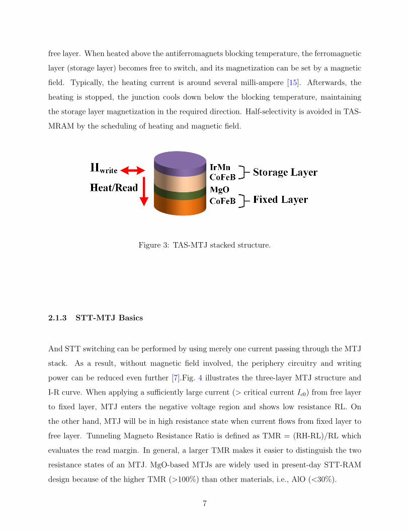
And STT switching can be performed by using merely one current passing through the MTJ
stack. As a result, without magnetic field involved, the periphery circuitry and writing
power can be reduced even further [7].Fig. 4 illustrates the three-layer MTJ structure and
I-R curve. When applying a sufficiently large current (> critical current Ic0) from free layer
to fixed layer, MTJ enters the negative voltage region and shows low resistance RL. On
the other hand, MTJ will be in high resistance state when current flows from fixed layer to
free layer. Tunneling Magneto Resistance Ratio is defined as TMR = (RH-RL)/RL which
evaluates the read margin. In general, a larger TMR makes it easier to distinguish the two
resistance states of an MTJ. MgO-based MTJs are widely used in present-day STT-RAM
design because of the higher TMR (>100%) than other materials, i.e., AlO (<30%).
7

Figure 4: (a) STT-MTJ stacked structure; (b) Illustration of static I-R curve of STT-MTJ.
2.2 MRAM CELL DESIGN
2.2.1 FIMS-and TAS-MRAM Cell
The typical FIMS-MRAM cell [6, 16] is illustrated in Fig. 5 . It consists of the MTJ connected
in series to the access transistor. The Bit Line (BL), Source Line (SL) and Bottom Write
Line 1 (WWL1) are shared along each column, while the Word Line (WL) and Top Write
Line 2 (WWL2) are shared among cells of the same row. During write operation, the uni-
directional current through WWL is activated as well as the bidirectional (data-dependent)
programming current through the BL. Since only at the orthogonal cross-point would there
be sufficient magnetic field, the selected cells state should switch. For read operation, a
small sense current runs through the MTJ to develop a voltage across the cell. This voltage
is evaluated by a Sense Amplifier (SA).
8

Figure 5: Typical FIMS-MRAM cell design.
TAS-MRAM shared the same cell structure with FIMS-MRAM as the writing field is
required. But the path of BL-MTJ-SL-NMOS is used for both read and heat operations in
TAS-MRAM.
2.2.2 STT-MRAM Cell
Figure 6 illustrates the “one-transistor-one-MTJ (1T1J)” STT-MRAM cell design adopted
in the STT-MRAM design where one NMOS access transistor is connected to the MTJ. The
NMOS transistor whose gate connects WL controls the access of the STT-MRAM cell and
supplies the read and write current passing through the MTJ. Compared with FIMS-MRAM
and TAS-MRAM, the reduced requirement of the MTJ write current amplitude help shrink
the size of the NMOS transistor and hence, resulting in a smaller STT-MRAM cell area.
9

Bit Line
MTJWord line
Source Line
sourcegate
drain
Figure 6: 1T1J STT-MTAM cell structure, 4X4 array.
During write operations of the STT-MRAM cell, proper voltage biases are applied to
the BL and the SL to control polarization of the write current. During read operations of
the STT-MRAM cell, a predetermined read current is applied to the MTJ. The generated
voltage on the BL is compared to a reference voltage, which is either generated from dummy
cells or outside signals.
2.3 MLC DESIGN FOR MRAM
2.3.1 STT-MLC-MRAM Design
Similar to Flash memory, MRAM designs also explored multi-level cell (MLC) technology to
store more than one data bit in a single cell: following the improvement on the distinction
between the lowest and the highest resistance states of the MTJ, making it possible to
further divide the MTJ resistance into multiple levels (two-bit cell typically) to represent
the combinations of multiple data bits [17, 18].
For STT-RAM, there are least two practical solutions of MLC MTJ structures [17, 18]
so far, including parallel MLC and series MLC. Fig. 7(a) and (b) show the structures of a
two-bit parallel MLC MTJ (a) and a two-bit series MLC MTJ (b), respectively.
10

In order to read out two-bit data, three reference voltage (current) and two sensing
operations are required to distinguish the target level among four possible situations. And
writing two-bit data also needs two steps: write both the two MTJs in the first step, write
back the softer MTJ in the second step [19, 20]. Due to the limited TMR, the STT-MLC-
MRAM can hardly achieve more than two bits storage for single cell to guarantee reliable
sensing. Because stacked MTJs cell design is vulnerable to read and write disturbance.
Figure 7: STT-MLC-MTJ design: (a) Parallel MLC configuration; (b) Series MLC configu-
ration.
2.3.2 TAS-MLC-MRAM Design
A recently proposed TAS-MRAM configuration [21, 22] naturally supports MLC design. Inthe storage element, TAS-MTJ , the pinned reference layer is replaced by a soft switchablereference layer, referred as the sense layer (Fig. 8). While the storage layer is similar asthat in FIMS-MTJ.
11

Figure 8: (a) TAS-MLC-MTJ structure; (b) Relationship between magnetization angles and
resistance levels.
MLC design for TAS-MRAM is more efficient than STT-MRAM: only one MTJ is em-
ployed in a MLC cell. Different resistance levels in TAS-MLC-MRAM are achieved by
different angles between storage layer and sense layer as Fig. 8 (b).
In general, the resistance corresponding to the relative angle of the magnetization direc-
tions of the storage layer and the sense layer can be calculated as [13]:
R =R
1 + TMR2
cos (θ1 − θ2). (2.1)
Here, θi (i=1 for the storage layer and 2 for the sense layer) is the angle between the
magnetization direction of each layer and the easy axis. R is the average resistance of the
TBC MTJ.
In writing operations, the storage layer is first unpinned by heating. Following the
increase of the device temperature, the exchange coupling between the CoFeB layer and the
IrMn layer becomes weaker. Then a magnetic field with an amplitude of several hundreds Oe
can be then applied to switch the magnetization of the CoFeB layer to one of eight possible
directions, as shown in Fig. 8(a). Magnetic direction is controlled by combinations of two
write line current with different amplitude, resulting a vector sum of different amplitude.
In reading operations, Instead of reading a resistance level as in STT-MLC-MRAM, or
a jump in resistance, as in regular self-referenced MRAM [23, 24], multi-bit self-referenced
TAS-MRAMs exploit the full resistance response obtained as the sense layer aligns itself
12

with an external rotating field [21, 22] while the magnetization of the CoFeB layer in the
storage layer is pinned. During this field rotation, the MTJ resistance continuously varies
as a function of the field angle.
A highest resistance (as shown in Fig. 8(b)) indicates the magnetization direction of
the storage layer, i.e. the information stored. With the angle of external field scanning
from 0 to 360, the order in which resistance values appear plays a role in the speed of
sensing, which provides the space for optimization. Thus, the data, stored in the storage
layer magnetization direction, can be read out from the phase of this oscillatory resistance,
for instance, by an external digital signal processor.
Without affecting the storage layer, different relative magnetization directions between
storage and sense layer yields different resistances due to Tunnel Magnetoresistance Effect.
In general, the resistance corresponding to the relative angle of the magnetization direc-
tions of the storage layer and the sense layer can be calculated as [13]:
R =R
1 + TMR2
cos (θ1 − θ2). (2.2)
θi (i=1 for the storage layer and 2 for the sense layer) is the angle between the magnetization
direction of each layer and the easy axis. R is the average resistance of the TBC MTJ.
Based on the measured data from[13], we created a micromagnetic model and simulate
the theoretical results of the TBC MTJ at different relative angle of the magnetization
directions of the storage layer and the sense layer, as shown in Fig. 8(b). Here the resistance
R is normalized as R = R−RLow
RHigh−RLow, where RHigh and RLow are the upper and lower bounds
of the TBC MTJ resistance, respectively. Our theoretical results fit the measured data very
well.
13
3.0 SENSING SCHEME EXPLORATION FOR MLC MRAM
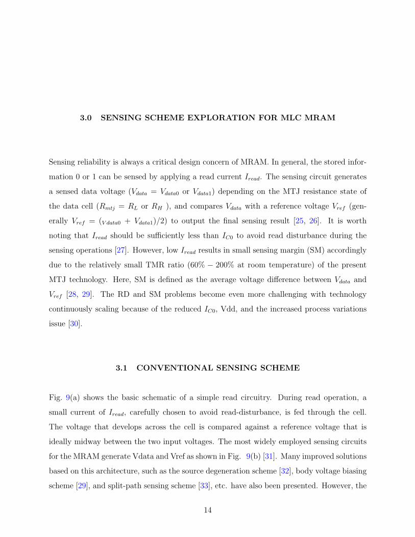
Sensing reliability is always a critical design concern of MRAM. In general, the stored infor-
mation 0 or 1 can be sensed by applying a read current Iread. The sensing circuit generates
a sensed data voltage (Vdata = Vdata0 or Vdata1) depending on the MTJ resistance state of
the data cell (Rmtj = RL or RH ), and compares Vdata with a reference voltage Vref (gen-
erally Vref = (V data0 + Vdata1)/2) to output the final sensing result [25, 26]. It is worth
noting that Iread should be sufficiently less than IC0 to avoid read disturbance during the
sensing operations [27]. However, low Iread results in small sensing margin (SM) accordingly
due to the relatively small TMR ratio (60% − 200% at room temperature) of the present
MTJ technology. Here, SM is defined as the average voltage difference between Vdata and
Vref [28, 29]. The RD and SM problems become even more challenging with technology
continuously scaling because of the reduced IC0, Vdd, and the increased process variations
issue [30].
3.1 CONVENTIONAL SENSING SCHEME
Fig. 9(a) shows the basic schematic of a simple read circuitry. During read operation, a
small current of Iread, carefully chosen to avoid read-disturbance, is fed through the cell.
The voltage that develops across the cell is compared against a reference voltage that is
ideally midway between the two input voltages. The most widely employed sensing circuits
for the MRAM generate Vdata and Vref as shown in Fig. 9(b) [31]. Many improved solutions
based on this architecture, such as the source degeneration scheme [32], body voltage biasing
scheme [29], and split-path sensing scheme [33], etc. have also been presented. However, the
14

intrinsic variation and device mismatch of Vref and Vdata branches keeps a problem below
40nm technology. This variation, especially in storage as well as reference cell and sensing
amplifier will induce sensing error, long sensing latency and larger error correction circuitry
overhead.
Figure 9: (a) Sketch of typical read scheme; (b) Schematic of the conventional read circuit
for STT-MRAM.
3.2 TYPICAL SELF REFERENCING SENSING SCHEME
Some self-reference schemes (destructive and non-destructive) are proposed. In the destruc-
tive self-reference scheme: 1) sense the state of an MTJ and store the result (i.e., as a voltage
level of a capacitor); 2) write a reference value to the MTJ; 3) sense the corresponding refer-
ence state of the MTJ and compare it to the stored result in step 1 to get the original MTJ
state; 4) write back the original state to the MTJ. This raises the concerns about the chip
reliability from non-volatility point of view. Also, the long read latency and the high power
consumption of conventional self-reference scheme (mainly due to the two write steps) are
15

commercially unattractive. While in the non-destructive self-reference scheme [23]:1) read
current IR1 is applied to generate BL voltage VBL1, which will be stored in C1. VBL1 can be
either VBL,L1 or VBL,H1, which are the BL voltages when the MTJ is at the low resistance
state or the high resistance state, respectively; 2) Another read current IR2 is applied and
generates BL voltage VBL2; 3) VBL1 and VBL2 are compared by the voltage sense amplifier.
If VBL1 is significantly larger than VBL2, the original value of STT-MRAM bit is “1” (high
resistance state). Otherwise, the original value of STT-MRAM bit is “0” (low resistance
state). Although the original state of an MTJ still needs to be read twice, there is no need
to write any reference value into the MTJ. Consequently, the long write back operation is
avoided. Compared to the conventional self-reference scheme, this technique improves the
memory reliability and reduces the read latency.
Despite of variation tolerance, the two types of self-reference sensing schemes can hardly
work in case of MLC-MRAM. While the novel TBC-MRAM structure described in above
chapters was intrinsically compatible with self-reference sensing. Total eight different rela-
tive magnetization relationships between storage layer and sense layer can be achieved to
represent a 3-digit data. Instead of reading a resistance level, or a change in resistance, as in
regular self-referenced MRAM, multi-bit self-referenced TAS-MRAMs exploit the full resis-
tance response obtained as the sense layer aligns itself with an external rotating field. During
this field rotation, the MTJ resistance continuously varies as a function of the field angle
(see Fig. 8), reaching a maximum (respectively, minimum) value when the sense and storage
layers moments become antiparallel (respectively, parallel). However, the TBC-MRAM self-
reference sensing scheme [13, 22] involves 8 times of programming and comparison to find
the largest or smallest resistance state, i.e., the original storage state.
3.3 THREE STEP SENSING SCHEME
In this work, a innovative Three Step Self-Reference Sensing (TSSRS) scheme is proposed,
sensing resistance order rather than measuring the real resistance value through direct com-
parisons.
16
Compared to conventional design [13], the performance, energy consumption, and relia-
bility of read operations can be dramatically improved.
In TSSRS, we tend to detect the stored data by comparing the MTJ resistances un-
der different magnetic fields. As in TAS-MLC-MRAM, a TLC MTJ has 8 different states
corresponding to 8 magnetization angles. However, there are only five distinct resistance
levels as shown in Fig. 8(b). To maximize the sensing margin and hence improve sensing
performance, we choose the following 8 angles that equalize the resistance difference between
any two adjacent levels: 0, 90.2, 116.9, 141.4, 180, -141.4, -116.9 and -90.2.
Table 1: States Truth Table
Original State 116.9 −141.4 −90.2 Output of SA Binary Code
#1 5 6 8 000 000
#2 4 7 7 XXX 001
#3 5 8 6 010 010
#4 6 7 5 011 011
#5 6 5 7 100 100
#6 7 4 6 101 101
#7 8 5 5 XXX 110
#8 7 6 4 111 111
Here, it is proposed to apply three magnetic fields with θ=141.4, -116.9, and 0 to the
sense layer in sequence. Consequently, the magnetization of the sense layer will be changed
three times in a row, corresponding to three resistance levels, respectively. As shown in
Table 1, the data stored in the device can be measured based on the order of the relative
relation of the three resistance values. For instance, if the first resistance is less than the
17
second while the last step obtains the highest resistance, the stored data correspons to #1
in Fig. 8(b). Here, the 8 types of orders are labeled as #1,. . . ,#8. As listed in Table I, 6
states can be detected based on the permutations of three resistance levels. States #2 and
#7 can not be distinguished by following the same rule. However, the resistance of #2(#7)
obtained in the first step is the highest (lowest) level. So we introduce two thresholds to
measure the first sensing. If the results of the first sensing is recognized the highest (lowest)
resistance state, the output 001 (100) is achieved instantly without further operation.
Figure 10: (a) Sensing Direction for three steps; (b) Processing Flow depicting the proposed
sensing methodology.
Here is an instance explaining the TSSRS methodology (Fig. 10(b)): If the direction
of storage layer is in state of #1, the first sense will give us a resistance of 5 because the
sensing field is in the direction of 2, like this. The difference of angle shows resistance of 5
as the cosine shaped curve shows. In the second step, the sensing field is in the direction
of number 6, gives us a resistance of six, and similarly, the third resistance level should be
eight, as the Table 1 shows. And the compared results of three steps are 000, because first
one is smaller than second one, first one is smaller than the third one and the second one
is smaller than the third one. In the case of state 2 and state 8, the initial resistance is the
lowest and highest respectively. It will obtain the three bits output immediately.
18

In this way, the TSSRS scheme successfully associate the eight states with the order of
three resistance instead of their values.
In summary, the proposed sensing scheme shall apply magnetic filed for at most three
times, or even no magnetic field required in 2 out of 8 cases, it will conduct at most five
comparisons, at least two comparisons. On the contrary, the traditional scheme will need 8
times of magnet field rotating and 8 comparisons in total. Dramatic improvement is achieved
by using the proposed TSSRS scheme.
19

4.0 SENSING CIRCUIT DESIGN FOR TLC MRAM SENSING
4.1 SENSE AMPLIFIER DESIGN
Figure 11(a) depicts the schematic of our SA design. Prior to read, port PC is asserted to
ground, pre-charging OUT and OUT to Vdd. After that, sensed voltage (Vcell) is applied
on port IN and the reference voltage Vref is applied to port Ref. Then a sense enable signal
SAN turns on transistor M7, commencing discharging OUT and OUT. If Vcell is larger than
Vref , for example, the left branch of the SA discharges more quickly than the right branch.
As a result, OUT will be grounded and OUT will be pulled up to Vdd. Fig. 12 presents the
transient response of a successful sensing.
Figure 11: (a) Schematic of SA; (b) Layout of SA.
20
Figure 12: Transient response of SA.
To accelerate the discharging speed of the branches of the SA, M5, M6 and M7 are espe-
cially sized up, as shown in Figure 11(b). The large transistor size also helps to mitigate the
impact of the device mismatch between the two branches and improve the sensing reliability.
4.2 TSSRS CIRCUITRY DESIGN
The sensing circuit for the proposed TSSRS scheme is presented in Fig. 13. For each step,
the sensed out voltage signals are stored in capacitors (C1 and C1′ , C2 and C2′ , C3 and C3′)
respectively. Before initializing the sensing circuit, the six capacitors are reset by connecting
them between Vreset and Gnd. The input terminals of sense amplifier are clamped to Vreset
too.
STEP 1 when the magnetic field of θ=116.9 is applied: We turn off SR1 and SR1′ , but
turn on S0 and S0. In this way, the sensing voltage V1 is applied to the bottom ends of the
C1 and C1′ and the top ends of the two capacitors shift from Vreset to Vreset+V1. Such a
structure boosted the stored voltage beyond the threshold voltage of sense amplifier (SA),
21
making sensing faster. Afterwards, S11 and S00′ are enabled and Vreset+V1 is compared with
Vref1. Then, we switch S11′ and S00 on to compare Vreset+V1 and Vref2. The design of
connecting Vreset to the two inputs of SA through separated paths can facilitate to avoid
mismatch of SA. At the end, S1 and S1′ are turned off to complete the step. If the lowest or
highest resistance is sensed out, then the 3-bit information can be directly obtained without
the following steps.
STEP 2 with the sensing magnetic field of θ=-141.4: If the resistance obtained in
previous step is neither the lowest nor the highest state, the design enters to the second step.
In the same way as V1 does, Vreset to Vreset+V2 is stored on C2 and C2′ simultaneously. Then
V1 and V2 are compared by connecting C1 and C2′ to SA.
STEP 3 with the sensing magnetic field of θ=-90.2 follows the similar routine as the
second step. First, store Vreset+V3 in C3 and C3′ . Then use C1′ and C3 to compare V1 and
V3. At last, compare V2 and V3 by connecting C2 and C3′ to SA. In this way, the order of
resistance levels of three sensing can be detected. And corresponding 3-bit information can
be obtained according to the Table 1 by utilizing certain basic logic gates.
Figure 13: Schematic of the proposed scheme.
22

5.0 SIMULATION AND SENSING PERFORMANCE ANALYSIS
Functional transient simulation and 100,000 Monte-Carlo simulations was conducted under
Cadence Virtuoso environment to analyze the effectiveness and reliability of the proposed
TLC MRAM reading scheme. The sensing circuit is designed at 0.13µm technology node.
A Verilog-A model for TBC MTJ was created by referring to [13]. The major factors of
variations and the assumption used in the work are summarized in TABLE 2.
Table 2: Variables and Parameters
Parameter Mean Value Standard Deviation
Resistance Area Product (Ω · µm2) 5.0 7%
Area of TLC-MTJ (nm2) 110× 200 5%× tech. node
Oxide Thickness (nm) 1.32 2%
TMR 1.0 5%
Transistor Width (nm) – 5%
Transistor Length (nm) 120 N/A
23
5.1 TSSRS SCHEME FUNCTIONAL SIMULATION
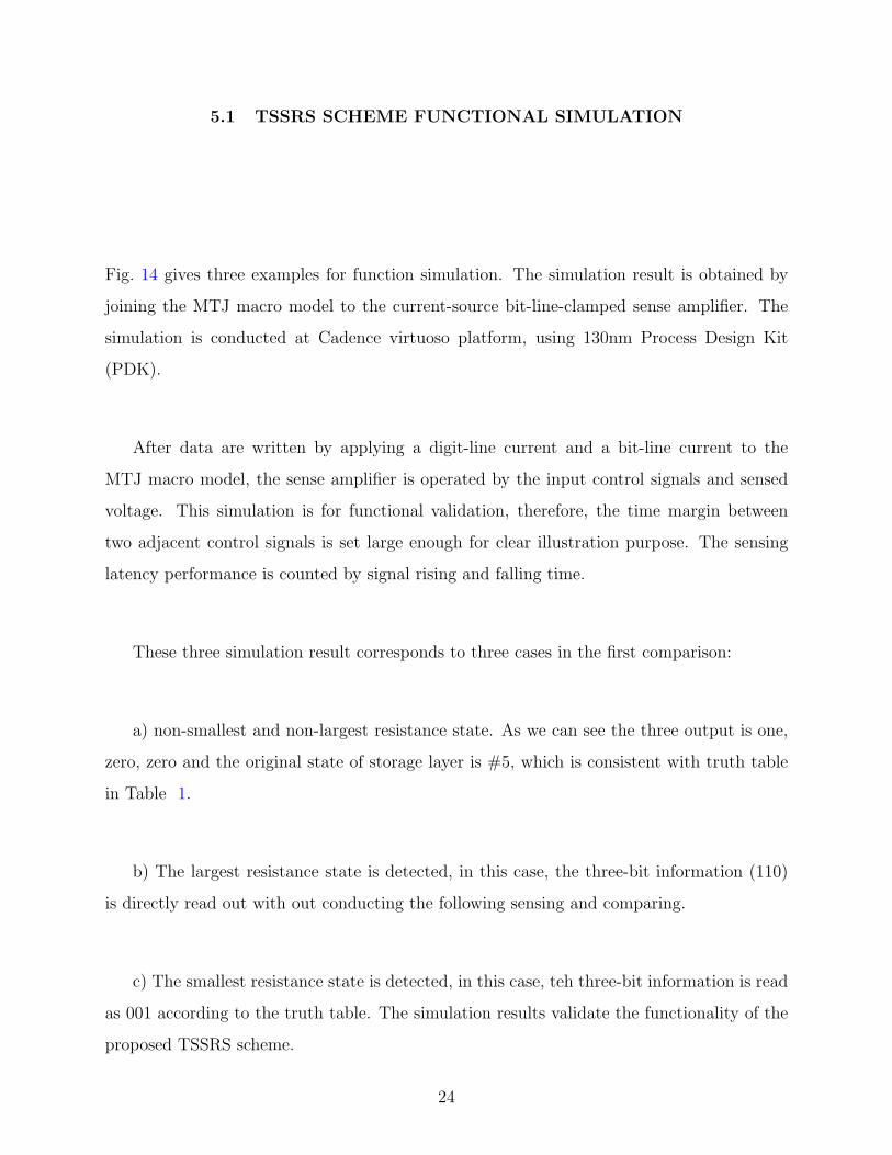
Fig. 14 gives three examples for function simulation. The simulation result is obtained by
joining the MTJ macro model to the current-source bit-line-clamped sense amplifier. The
simulation is conducted at Cadence virtuoso platform, using 130nm Process Design Kit
(PDK).
After data are written by applying a digit-line current and a bit-line current to the
MTJ macro model, the sense amplifier is operated by the input control signals and sensed
voltage. This simulation is for functional validation, therefore, the time margin between
two adjacent control signals is set large enough for clear illustration purpose. The sensing
latency performance is counted by signal rising and falling time.
These three simulation result corresponds to three cases in the first comparison:
a) non-smallest and non-largest resistance state. As we can see the three output is one,
zero, zero and the original state of storage layer is #5, which is consistent with truth table
in Table 1.
b) The largest resistance state is detected, in this case, the three-bit information (110)
is directly read out with out conducting the following sensing and comparing.
c) The smallest resistance state is detected, in this case, teh three-bit information is read
as 001 according to the truth table. The simulation results validate the functionality of the
proposed TSSRS scheme.
24
Figure 14: The transient response of TSSRS scheme: (a) Three steps sensing “#5”; (b)Two
comparisons of “#7”; (c) Two comparisons of “#2”.
25

5.2 IMPACTS OF PROCESS VARIATION ON TSSRS SCHEME
It is firstly investigated that the sensing voltage distributions at different resistance states for
both 3-bit MCL STT-MRAM and TBC MRAM. In this experiment, the 3-bit MLC STT-
MRAM follows the conventional structure, in which three MTJs in different dimensions
are serially stacked. The statistical data in Fig. 15(a) shows that after considering process
variations, wide distribution of the sensing voltages can be observed for all the resistance
states. Considering the limited gap between adjacent states, the overlap of their sensing
voltages is quite large, leading to high read error rate.
The sensing voltage distribution of TBC MRAM is shown in Fig. 15(b). It is worthy
mentioning that the proposed reading design is indeed a self-reference scheme, which detect
the stored data of one single cell by comparing its own intermediate states. As such, the
read error induced by the cell-to-cell variations can be precluded. The only exceptions are
states #4 and #8 that are determined by one-step sensing. Fortunately, sufficient sensing
margins can be obtained for the resistance levels at both ends by carefully selecting the
relative coordinate system, which is demonstrated by our simulation results in Fig. 15(b).
In Fig. 15(c), the read error rates of 3-bit MLC STT RAM and TBC MRAM has been
compared within a 5% to 9% standard deviation range of variation factors are small (e.g.
less than 6%), the result can not be easily obtained by the Monte Carlo simulation, thus,
we fit the curve to get the result of 5% variation. For the aforementioned reason, the read
reliability of TBC MRAM is much better than that of MLC STT-MRAM. As the standard
deviation of both MTJ area and access transistor increases, the error rate of TBC MRAM
rises close to MLC STT RAM, Even though, with a 9% variation, TBC MRAM still has 100
times less in terms of reading error rate.
26

Sensed Voltage (mV)
Pro
bab
ilit
y (
%)
20
40
60
760 800 840
Sensed Voltage (mV)840 860 880
(a)P
rob
abil
ity
(%
)
20
40
60(b)
900
1 2 3 4 5 6 7 8
4 5(3) 6(2) 7(1) 8
(c)100
10-1
10-2
10-3
10-4
10-5
10-6
1 2 3 4 5E
rror
Rat
e
Standard Deviation σ (%)
Figure 15: The sensing voltage distributions of (a) the conventional MLC STT-MRAM and
(b) TBC MRAM. Note that TBC MRAM has only 5 distinct resistance states; (c) The error
rate vs. the standard deviation of key parameters.
5.3 THERMAL DEPENDENCY IN READING OPERATION
The TSSRS scheme for TBC MRAM could be sensitive to environment temperature that
affects the characteristics of both MTJ and transistor. Fig. 16 shows the trend of the sensing
margins of all the eight states with the increment of temperature.
27

30
22.5
15
7.5
0
-7.5225 250 275 300 325 350 375 400
#1
#8 #7 #6 #5
#2 #3 #4
Temperature (K)
Mar
gin
(m
V)
Figure 16: Temperature-dependent sensing margin.
In general, the sensing margin reduces as temperature raises up. This is because the read
current becomes smaller as the performance of transistors degrades at high temperature. In
addition, the discharge on capacitors is faster due to aggravated leakage, which may distort
the sensing results: a sensing voltage stored earlier will be much smaller than what it is
supposed to be when comparing with another one stored later.
However, in some particular situation, the capacitance discharge may distort the sensing
results: a sensing voltage stored earlier will be much smaller than what it is supposed to be
when comparing with another one stored later. This explains the sensing margins of #1 and
#3 increases as environment temperature exceeds 325K.
The study in Fig. 16 shows that the proposed sensing scheme can maintain the sensing
margin greater than 7mV as temperature is lower than 350K, which is an acceptable range
for on-chip memory.
28

6.0 CONCLUSION
In this work, an innovative self-reference sensing scheme was proposed for the newly invented
TBC-MRAM cell by utilizing its unique property of state ordering. This design eliminates
the impact of cell-to-cell variation, significantly improve the read reliability, and reduce the
sensing delay and energy cost w.r.t. conventional design. Highly improve the performance of
sensing latency and energy consumption compared with the ordinary 8-step sensing by only
sensing three times to read 3 bits. The analysis on the impact of process variation on the
read margin and its temperature dependency are also performed to explore the design space
of the proposed scheme. Simulation results show that our design perfectly utilize the unique
property of the TBC-MRAM cell, In addition, the proposed sensing scheme mitigates margin
degrading induced by process variation which significantly deteriorates sensing reliability of
STT-MLC-MRAM. And with Cadence simulation platform, we analyze sensing performance
of delay and margin and take into account thermal effects, validating the effectiveness and
high reliability of the proposed three-step sensing scheme.
29

BIBLIOGRAPHY
[1] R. Rodriguez, J. Stathis, B. Linder, S. Kowalczyk, C. Chuang, R. Joshi, G. Northrop,K. Bernstein, A. Bhavnagarwala, and S. Lombardo, “The impact of gate-oxide break-down on sram stability,” Electron Device Letters, vol. 23, no. 9, pp. 559–561, 2002.
[2] K. C. Chun, H. Zhao, J. D. Harms, T.-H. Kim, J.-P. Wang, and C. H. Kim, “A scalingroadmap and performance evaluation of in-plane and perpendicular mtj based stt-mramsfor high-density cache memory,” IEEE Journal of Solid-State Circuits, vol. 48, no. 2,pp. 598–610, 2013.
[3] B. Dieny, R. Sousa, J. Herault, C. Papusoi, G. Prenat, U. Ebels, D. Houssameddine,B. Rodmacq, S. Auffret, L. B. Prejbeanu, M. Cyrille, B. Delaet, O. Redon, C. Ducruet,J. P. Nozieres, and I. Prejbeanu, “Spin-transfer effect and its use in spintronic compo-nents,” 2010.
[4] G. Jan, L. Thomas, S. Le, Y.-J. Lee, H. Liu, J. Zhu, R.-Y. Tong, K. Pi, Y.-J. Wang,D. Shen, R. He, J. Haq, J. Teng, V. Lam, K. Huang, T. Zhong, T. Torng, and P.-K.Wang, “Demonstration of fully functional 8Mb perpendicular STT-MRAM chips withsub-5ns writing for non-volatile embedded memories,” in 2014 Symposium on VLSITechnology (VLSI-Technology): Digest of Technical Papers, pp. 1–2, IEEE, June 2014.
[5] Y. Chen, W.-F. Wong, H. Li, C.-K. Koh, Y. Zhang, and W. Wen, “On-chip caches builton multilevel spin-transfer torque RAM cells and its optimizations,” ACM Journal onEmerging Technologies in Computing Systems, vol. 9, pp. 1–22, May 2013.
[6] B. Engel, J. Akerman, B. Butcher, R. Dave, M. DeHerrera, M. Durlam, G. Grynkewich,J. Janesky, S. Pietambaram, N. Rizzo, et al., “A 4-mb toggle mram based on a novel bitand switching method,” IEEE Transactions on Magnetics, vol. 41, no. 1, pp. 132–136,2005.
[7] C. Lin, S. Kang, Y. Wang, K. Lee, X. Zhu, W. Chen, X. Li, W. Hsu, Y. Kao, M. Liu,et al., “45nm low power cmos logic compatible embedded stt mram utilizing a reverse-connection 1t/1mtj cell,” in Electron Devices Meeting (IEDM), 2009 IEEE Interna-tional, pp. 1–4, IEEE, 2009.
[8] R. Beach, T. Min, C. Horng, Q. Chen, P. Sherman, S. Le, S. Young, K. Yang, H. Yu,X. Lu, et al., “A statistical study of magnetic tunnel junctions for high-density spin
30

torque transfer-mram (stt-mram),” in Electron Devices Meeting, 2008. IEDM 2008.IEEE International, pp. 1–4, IEEE, 2008.
[9] I. Prejbeanu, M. Kerekes, R. Sousa, H. Sibuet, O. Redon, B. Dieny, and J. Nozieres,“Thermally assisted mram,” Journal of Physics: Condensed Matter, vol. 19, no. 16,p. 165218, 2007.
[10] T. Min and P.-K. Wang, “Multi-state thermally assisted storage,” Mar. 18 2008. USPatent 7,345,911.
[11] T. Hanyu, “Challenge of MTJ/MOS-hybrid logic-in-memory architecture for nonvolatileVLSI processor,” in Circuits and Systems (ISCAS), 2013 IEEE International Sympo-sium on, pp. 117–120, IEEE, 2013.
[12] M. Aoki, H. Noshiro, K. Tsunoda, Y. Iba, A. Hatada, M. Nakabayashi, A. Takahashi,C. Yoshida, Y. Yamazaki, T. Takenaga, and T. Sugii, “Novel highly scalable multi-levelcell for STT-MRAM with stacked perpendicular MTJs,” pp. T134–T135, 2013.
[13] Q. Stainer, L. Lombard, K. Mackay, D. Lee, S. Bandiera, C. Portemont, C. Creuzet,R. C. Sousa, and B. Dieny, “Self-referenced multi-bit thermally assisted magnetic ran-dom access memories,” Applied Physics Letters, vol. 105, p. 032405, July 2014.
[14] Z. Diao, D. Apalkov, M. Pakala, Y. Ding, A. Panchula, and Y. Huai, “Spin trans-fer switching and spin polarization in magnetic tunnel junctions with mgo and alo xbarriers,” Applied Physics Letters, vol. 87, no. 23, p. 232502, 2005.
[15] R. L. Stamps, S. Breitkreutz, J. kerman, A. V. Chumak, Y. Otani, G. E. W. Bauer,J.-U. Thiele, M. Bowen, S. A. Majetich, M. Klui, I. L. Prejbeanu, B. Dieny, N. M.Dempsey, and B. Hillebrands, “The 2014 magnetism roadmap,” Journal of Physics D:Applied Physics, vol. 47, no. 33, p. 333001, 2014.
[16] S. Tehrani, J. Slaughter, E. Chen, M. Durlam, J. Shi, and M. DeHerren, “Progressand outlook for mram technology,” IEEE Transactions on Magnetics, vol. 35, no. 5,pp. 2814–2819, 1999.
[17] T. Ishigaki, T. Kawahara, R. Takemura, K. Ono, K. Ito, H. Matsuoka, and H. Ohno,“A multi-level-cell spin-transfer torque memory with series-stacked magnetotunnel junc-tions,” in VLSI Technology (VLSIT), 2010 Symposium on, pp. 47–48, IEEE, 2010.
[18] X. Lou, Z. Gao, D. V. Dimitrov, and M. X. Tang, “Demonstration of multilevel cell spintransfer switching in mgo magnetic tunnel junctions,” Applied Physics Letters, vol. 93,no. 24, p. 242502, 2008.
[19] Y. Zhang, L. Zhang, W. Wen, G. Sun, and Y. Chen, “Multi-level cell stt-ram: Is itrealistic or just a dream?,” in Computer-Aided Design (ICCAD), 2012 IEEE/ACMInternational Conference on, pp. 526–532, IEEE, 2012.
31

[20] X. Bi, M. Mao, D. Wang, and H. Li, “Unleashing the potential of mlc stt-ram caches,”in Computer-Aided Design (ICCAD), 2013 IEEE/ACM International Conference on,pp. 429–436, IEEE, 2013.
[21] Q. Stainer, L. Lombard, K. Mackay, R. Sousa, I. Prejbeanu, and B. Dieny, “Mram withsoft reference layer: In-stack combination of memory and logic functions,” in MemoryWorkshop (IMW), 2013 5th IEEE International, pp. 84–87, IEEE, 2013.
[22] I. Prejbeanu, S. Bandiera, J. Alvarez-Herault, R. Sousa, B. Dieny, and J. Nozieres,“Thermally assisted mrams: ultimate scalability and logic functionalities,” Journal ofPhysics D: Applied Physics, vol. 46, no. 7, p. 074002, 2013.
[23] Y. Chen, H. Li, X. Wang, W. Zhu, W. Xu, and T. Zhang, “A nondestructive self-reference scheme for spin-transfer torque random access memory (stt-ram),” in Design,Automation & Test in Europe Conference & Exhibition (DATE), 2010, pp. 148–153,IEEE, 2010.
[24] J.-T. Choi, G.-H. Kil, K.-B. Kim, and Y.-H. Song, “Novel self-reference sense amplifierfor spin-transfer-torque magneto-resistive random access memory,” Journal of Semicon-ductor Technology and Science, vol. 16, no. 1, pp. 31–38, 2016.
[25] W. Zhao, C. Chappert, V. Javerliac, and J.-P. Noziere, “High speed, high stability andlow power sensing amplifier for mtj/cmos hybrid logic circuits,” IEEE Transactions onMagnetics, vol. 45, no. 10, pp. 3784–3787, 2009.
[26] D. Gogl, C. Arndt, J. C. Barwin, A. Bette, J. DeBrosse, E. Gow, H. Hoenigschmid,S. Lammers, M. Lamorey, Y. Lu, et al., “A 16-mb mram featuring bootstrapped writedrivers,” IEEE Journal of Solid-State Circuits, vol. 40, no. 4, pp. 902–908, 2005.
[27] W. Zhao, Y. Zhang, T. Devolder, J.-O. Klein, D. Ravelosona, C. Chappert, and P. Ma-zoyer, “Failure and reliability analysis of stt-mram,” Microelectronics Reliability, vol. 52,no. 9, pp. 1848–1852, 2012.
[28] W. Kang, W. Zhao, J.-O. Klein, Y. Zhang, C. Chappert, and D. Ravelosona, “Highreliability sensing circuit for deep submicron spin transfer torque magnetic randomaccess memory,” Electronics Letters, vol. 49, no. 20, pp. 1283–1285, 2013.
[29] F. Ren, H. Park, C.-K. K. Yang, and D. Markovic, “Reference calibration of body-voltage sensing circuit for high-speed stt-rams,” IEEE Transactions on Circuits andSystems I: Regular Papers, vol. 60, no. 11, pp. 2932–2939, 2013.
[30] W. Kang, Z. Li, J.-O. Klein, Y. Chen, Y. Zhang, D. Ravelosona, C. Chappert, andW. Zhao, “Variation-tolerant and disturbance-free sensing circuit for deep nanometerstt-mram,” IEEE Transactions on Nanotechnology, vol. 13, no. 6, pp. 1088–1092, 2014.
32
[31] J. Kim, K. Ryu, S. H. Kang, and S.-O. Jung, “A novel sensing circuit for deep sub-micron spin transfer torque mram (stt-mram),” IEEE Transactions on very large scaleintegration (VLSI) systems, vol. 20, no. 1, pp. 181–186, 2012.
[32] D. Gogl, C. Arndt, J. C. Barwin, A. Bette, J. DeBrosse, E. Gow, H. Hoenigschmid,S. Lammers, M. Lamorey, Y. Lu, et al., “A 16-mb mram featuring bootstrapped writedrivers,” IEEE Journal of Solid-State Circuits, vol. 40, no. 4, pp. 902–908, 2005.
[33] J. Kim, T. Na, J. P. Kim, S. H. Kang, and S.-O. Jung, “A split-path sensing circuitfor spin torque transfer mram,” IEEE Transactions on Circuits and Systems II: ExpressBriefs, vol. 61, no. 3, pp. 193–197, 2014.
33