a plasmonic enhanced photodetector based on silicon nanocrystals obtained through laser ablation
TRANSCRIPT

This content has been downloaded from IOPscience. Please scroll down to see the full text.
Download details:
IP Address: 128.118.88.48
This content was downloaded on 08/11/2014 at 21:18
Please note that terms and conditions apply.
A plasmonic enhanced photodetector based on silicon nanocrystals obtained through laser
ablation
View the table of contents for this issue, or go to the journal homepage for more
2012 J. Opt. 14 125001
(http://iopscience.iop.org/2040-8986/14/12/125001)
Home Search Collections Journals About Contact us My IOPscience

IOP PUBLISHING JOURNAL OF OPTICS
J. Opt. 14 (2012) 125001 (5pp) doi:10.1088/2040-8978/14/12/125001
A plasmonic enhanced photodetectorbased on silicon nanocrystals obtainedthrough laser ablation
Sabri Alkis1,2, Feyza B Oruc1,2, Bulend Ortac1, A Cahit Kosger1,2 andAli K Okyay1,2
1 UNAM Institute of Materials Science and Nanotechnology, Bilkent University, Bilkent 06800 Ankara,Turkey2 Department of Electrical and Electronics Engineering, Bilkent University, Bilkent 06800 Ankara,Turkey
E-mail: [email protected] and [email protected]
Received 26 July 2012, accepted for publication 24 September 2012Published 18 October 2012Online at stacks.iop.org/JOpt/14/125001
AbstractWe present a proof-of-concept photodetector which is sensitive in the visible spectrum. Siliconnanocrystals (Si-NCs) obtained by laser ablation are used as the active absorption region.Si-NC films are formed from a polymeric dispersion. The films are sandwiched between thininsulating films to reduce the electrical leakage current. Furthermore, Ag nanoparticles areintegrated with the photodetector to enhance the visible response using plasmonic effects. Themeasured photocurrent is resonantly enhanced, which is explained in terms of enhanced localfields caused by localized plasmons. The UV–vis spectrum of Ag nanoparticles is alsomeasured to verify the resonance.
Keywords: photodetector, thin film, semiconductor nanocrystals, laser ablation
(Some figures may appear in colour only in the online journal)
1. Introduction
Silicon, despite its poor photodetection and generationproperties, remains an unrivaled material in the currentintegrated circuit industry because of its indirect bandgap.Ultra-small forms of silicon, however, exhibit excitingphotonic characteristics. Ultra-small Si nanocrystals (Si-NCs)show strong luminescence in the visible wavelengths [1–3].The cadmium-free nature of Si-NCs makes them primecandidates for solid-state and backlighting industries [4].Photodetectors have been fabricated based on Si-NCs andbandgap engineered with adjustments in NC size [5–8]. Kimet al made a significant step towards the development of newsilicon image sensors by showing that it is possible to developwavelength-sensitive photodetectors by adjusting the Si-NCsize [9]. In addition to the possibility of bandgap control withsize, Si-NCs provide very fast optical transition and multiplecarrier generation that paves the way to new and highly
efficient optoelectronic device fabrication [10, 11]. Cho et alinvestigated the size-dependent carrier injection dynamics inSi-NCs in a systematic approach and they observed strongsize-dependent characteristics of the carriers, due to quantumconfinement effects [12]. There is also a tremendous amountof effort to bring solar cell costs down to the levels of fossilfuels. Si-NCs are also promising candidates for bandgapengineered tandem solar cells owing to the size controlledbandgap and natural abundance of silicon. The recent workof Kim et al showed that the presence of Si-NCs provideda 14-fold increase in solar cell performance in the blue andgreen regions compared to bulk silicon, emphasizing theimportance of Si-NCs for tandem solar cell applications [13].
In the above-cited works, Si-NCs are synthesized bychemical vapor deposition (CVD) techniques that yield anarrow size distribution of nanoparticles. However, CVDprocesses require a vacuum environment and therefore thethroughput is limited. For large area photonics applications, a
12040-8978/12/125001+05$33.00 c© 2012 IOP Publishing Ltd Printed in the UK & the USA
J. Opt. 14 (2012) 125001 S Alkis et al
low cost and high throughput method is desirable. One of thepossible and efficient ways of synthesizing ultra-small Si-NCswith high concentration is the laser ablation method. Thismethod is widely used and it is promising for the synthesisof ultra-small Si-NCs in solution form [14–17]. During thelaser ablation process, the interaction of intense laser lightand matter makes NC synthesis possible, leading towards theformation of photoluminescent, ultra-small NCs with highconcentration [18–36]. Barcikowski et al showed that it ispossible to synthesize nanoparticles on a scale of severalgrams through the laser ablation method [37]. This work is agood indication of the feasibility of the laser ablation methodfor large-scale applications. The laser ablation techniquetypically results in a wider particle size distribution that couldbe used as a design advantage to achieve wideband absorptionin photovoltaic devices. Photoluminescence properties of thesynthesized Si-NCs are also reported in the literature andAlkis et al showed that it is further possible to reduce laserablated Si-NCs sizes and blue-shift their optical emissionsthrough an acid-free sonification and filtration post-treatmentprocedure [4, 22–24].
In this paper, we investigate the use of laser ablatedSi-NCs as active layers in optical detectors. A major obstaclefor efficient Si-NC PD fabrication is the insufficient ability ofSi-NCs to absorb light compared to Si wafer based PDs. Inorder to increase the light absorbed in Si-NCs and improvethe efficiency of Si-NC PDs, a possible route that could befollowed is to exploit increased local field intensity due tolocalized plasmons in metal nanoparticles [38]. Numerousoptoelectronic devices including silicon solar cells and siliconPDs with plasmonically enhanced efficiencies have beenrealized using metal NCs [39–43]. The recent work ofKim et al demonstrated a Si-NC PD based on 3 nm sizeSi-NCs in solid form that were obtained through plasmaenhanced chemical vapor deposition (PECVD) using SiH4and NH3 gases as precursors and they reported significantenhancements in the photocurrent values by localized modesin Ag NCs [44]. However, Si-NCs used in that work wereobtained in a solid host matrix inside a plasma chamber, undervacuum at elevated temperatures which limits the scalabilityand throughput for large area optoelectronic applications.
In this paper, we demonstrate a new Si-NC PD basedon Si-NCs that are synthesized through a single step laserablation in liquid form and we report the photocurrentenhancement with the use of Ag nanoparticles. A schematicrepresentation of the fabricated Si-NC PD is given and theelectrical measurement results are supported by SEM imagesand UV–vis spectra.
2. Experimental details
Colloidal 5–100 nm Si-NCs used in this work were generatedusing a commercial nanosecond pulsed ND:YLF laser(Empower Q-Switched Laser, Spectra Physics) operated at527 nm with pulse duration of 100 ns, average output powerof 16 W at a pulse repetition rate of 1 kHz corresponding toa pulse energy of 16 mJ. The laser beam was focused on ap-type Si wafer target placed in a glass vial containing 20 ml
of de-ionized water using a plano-convex lens with a focallength of 50 mm. The height of the liquid layer over the Sitarget was about 5 mm. The laser ablation was carried out for5 min. Optical properties and size distributions of laser ablatedSi-NCs are given in greater detail in our previously publishedmanuscript [4].
Si-NC PD fabrication was performed on highly p-type(0.010–0.018 � cm boron doped) Si substrate. The substratewas cleaned through standard cleaning procedures involvingacetone, isopropanol and water. 10 nm of Ag thin filmwas thermally evaporated (VAKSIS-MIDAS) on Si substratefollowed by rapid thermal annealing (ATV RTA-SRO-704)of the sample in the presence of N2 gas at 600 ◦C for65 s. This was done in order to form ultra-small Ag-NCson the Si substrate [44]. This was followed by depositionof 7 nm Al2O3 on the Ag-NCs/Si structure by atomic layerdeposition (ALD) for isolation. The ALD process was donewith a Cambridge Nanotech Savannah 100 type commercialALD instrument using (CH3)3Al and H2O as the precursorgases at 250 ◦C. In order to form a thin film of Si-NCson top of the Al2O3/Ag-NCs/Si structure, 2 g of polyvinylalcohol (Mowiol 10-98, Aldrich Chemicals) was added to a20 ml Si-NCs/water solution that was prepared through laserablation. The solution was stirred vigorously at 90 ◦C for48 h in order to dissolve the added polymer and obtain ahomogeneous solution. The sample surface was then coatedwith the prepared Si-NC solution using dip-coating witha home-built dip-coat instrument at an operating speed of1.7 mm s−1. The dip-coat procedure was repeated for tencycles in order to form Si-NC films. In this work, there was noattempt to optimize the film uniformity of the Si-NC film. Thisprocedure was followed by a second ALD of 7 nm Al2O3 ontop of the Si-NCs/Al2O3/Ag-NCs/Si structure using the sameALD recipe. A thin (<10 nm) Al layer was evaporated on topof the sandwich structure for charge collection followed byactive area patterning by photolithography. Finally, 75 nm Alwas evaporated to form the front and back contacts. In orderto observe the Ag-NC effects on the performance of Si-NCsPDs, two sets of Si-NC PDs were fabricated. Samples withoutAg-NCs are used as reference PDs.
3. Results and discussions
Figure 1 shows the cross-sectional illustration and a scanningelectron microscope (SEM) image of a completed device. Thebottom Al layer and the highly p-type doped Si substrate areused as the back electrode. The Al2O3 layers are chosen thinto allow for tunneling of photogenerated carriers. The topaluminum layer is kept thin to allow for light penetration intothe active area.
Figure 2(a) shows a typical SEM image (FEI NovaNanosem 430) of the Ag-NCs formed on glass substrateafter RTA treatment. Particle sizes 20–150 nm are observedwith a distribution as shown in the inset. The absorptioncharacteristics of the Ag-NC thin film formed with the abovetechnique were obtained with a Varian Cary 5000 UV/vis/NIRspectrophotometer. The spectral absorption of the Ag-NCfilms, figure 2(b), exhibits a broad absorption peak centered
2

J. Opt. 14 (2012) 125001 S Alkis et al
Figure 1. (a) Cross-sectional diagram of the fabricated Si-NC PD.(b) SEM image, top view of the fabricated Si-NC PD.
around 490 nm. Ag-NCs absorb light into localized plasmonmodes as explained earlier [44]. In the completed device,the Ag-NCs are obtained on Si substrate and are covered bya Al2O3 layer. The absorption peak is expected to shift tolarger wavelengths due to the higher refractive indices of thesurrounding materials (compared to Ag-NCs on glass).
The electrical characterization of the fabricated deviceswas performed with a commercial Keithley 4200-SCS typesemiconductor parameter analyzer. Current–voltage (I–V)
characteristics were obtained under dark conditions as shownin figure 3. The measured dark current densities of thedevices are low, 30 mA cm−2, owing to the dual Al2O3insulating layers. The dark current characteristics for sampleswith Ag-NCs show a characteristic increase of current after5 V bias. This is attributed to the higher number of statesavailable for charge tunneling owing to the presence ofAg-NC induced states at the Si–Al2O3 interface. Repeatableand scalable electrical characteristics obtained from differentdevices verify repeatable Si-NC coating.
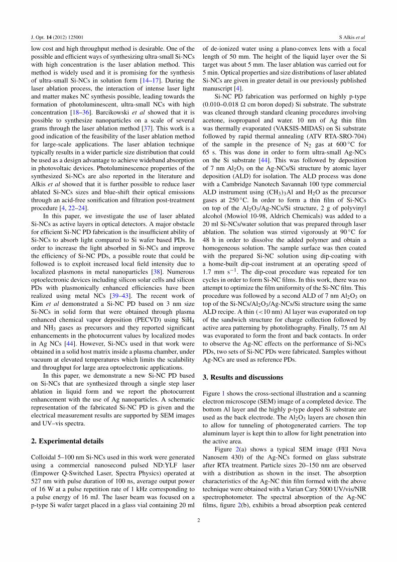
Spectral photogenerated current (Iphoto) is measured at2 V applied electrical bias with a mechanically chopped,monochromated light normally incident on the device surfaceand a lock-in amplifier (SRS 830). Incident light power (Pin)
was measured with a calibrated Si photodetector. We useda bias voltage of 2 V in our photocurrent measurements.The measured photocurrent values are low compared to theliterature [44]. This is attributed to the reduced collectionefficiency of the photogenerated electron–hole pairs due tothe presence of the dual Al2O3 layers that electrons andholes should tunnel through. Figure 4 plots the normalizedphotogenerated current versus light wavelength from deviceswith and without a Ag-NC layer. The presence of Ag-NCs
Figure 2. (a) SEM image, Ag islands on quartz glass, inset: sizedistribution of Ag islands. (b) UV–vis absorption spectrum of Agislands on quartz.
Figure 3. Dark current (I) versus bias voltage (V) spectrum, topcurve Si-NC PD with Ag (solid line), bottom curve (dashed line)Si-NC PD without Ag.
introduced an additional peak around 550–570 nm. This isattributed to the plasmon resonance of Ag-NCs, which is inperfect agreement with the absorption profile of Ag-NCs asshown in figure 2(b). The absorption peak associated with
3
J. Opt. 14 (2012) 125001 S Alkis et al
Figure 4. Normalized photogenerated current versus wavelength(nm) spectrum: top curve Si-NC PD with Ag; bottom curve Si-NCPD without Ag.
Ag-NCs is red-shifted as predicted above, due to the largerdielectric constant of the surrounding Si substrate (comparedto glass) and Al2O3 (compared to air), and a correspondingshift of the localized plasmon resonance (from around 500 to550 nm).
4. Conclusion
Visible range photodetectors are experimentally demonstratedusing ultra-small Si-NCs obtained by laser ablation. Si-NCsfilms are achieved by the dip-coating technique. Theabsorption of the Si-NC layer is enhanced by Ag-NCs usinglocalized plasmonic modes. Such Si-NCs could be used forultra-low cost optoelectronic devices such as flexible anddisposable sensors and low cost solar cells. Photodetectorsthat are fabricated based on such Si-NCs could offer newadvantages over other types of photodetectors that arebased on plasma-grown Si-NCs in large area optoelectronicsapplications by providing greater throughput and scalability.
Acknowledgments
This work was supported in part by European UnionFramework Program 7 Marie Curie IRG Grant 239444,COST NanoTP, TUBITAK Grants 108E163, 109E044,112M004 and 112E052, Ministry of Industry and Trade636.STZ.2010-1. The State Planning Organization (DPT) ofTurkey is acknowledged for the support from the UNAMInstitute of Materials Science and Nanotechnology and theauthors acknowledge support from TUBITAK BIDEB. Theauthors also thank Mr Adem Sarac for the SEM imagingand Mr Semih Yasar for his kind support with cleanroomexperiments.
References
[1] Akcakir O, Therrien J, Belomoin G, Barry N, Muller J D,Gratton E and Nayfeh M 2000 Appl. Phys. Lett. 76 1857
[2] Mitas L, Therrien J, Twesten R, Belomoin G andNayfeh M 2000 Appl. Phys. Lett. 78 1918
[3] Rogozhina E, Belomoin G, Smith A, Abuhassan L, Barry N,Akcakir O, Braun P V and Nayfeh M 2001 Appl. Phys. Lett.78 3711
[4] Alkis S, Okyay A K and Ortac B 2012 J. Phys. Chem. C116 3432
[5] Hirano Y, Sato F, Aihara S, Saito N, Miyazaki S andHirose M 2001 Appl. Phys. Lett. 79 2255
[6] Nayfeh M H, Satish R, Nayfeh O M, Smith A andTherrien J 2005 IEEE Trans. Nanotechnol. 4 660
[7] Shieh J M, Lai Y F, Ni W X, Kuo H C, Fang C Y,Huang J Y and Pan C L 2007 Appl. Phys. Lett. 90 051105
[8] Hu S F, Liao T W and Huang C Y 2007 Appl. Phys. Lett.91 071125
[9] Kim S K, Kim B H, Cho C H and Park S J 2009 Appl. Phys.Lett. 94 183106
[10] Takagahara T and Takeda K 1992 Phys. Rev. B 46 15578[11] Beard M C, Knutsen K P, Yu P, Luther J M, Song Q,
Metzger W K, Ellingson R J and Nozik A J 2007 NanoLett. 7 2506
[12] Cho C H, Kim S K, Kim B H and Park S J 2009 Appl. Phys.Lett. 95 243108
[13] Kim S K, Cho C H, Kim B H, Park S J and Lee J W 2009Appl. Phys. Lett. 95 143120
[14] Mafune F, Kohno J, Takeda Y, Kondow T and Sawabe H 2000J. Phys. Chem. B 104 8333
[15] Muramoto J, Inmaru T, Nakata Y, Okada T andMaeda M 2000 J. Phys. Chem. B 104 9111
[16] Mafune F, Kohno J, Takeda Y, Kondow T and Sawabe H 2001J. Phys. Chem. B 105 5114
[17] Dolgaev S I, Simakin A V, Voronov V V, Shafeev G A andBozon-Verduraz F 2002 Appl. Surf. Sci. 186 546
[18] Yoshida T, Yamada Y and Takaaki O 1998 J. Appl. Phys.83 5427
[19] Ehbrecht M, Kohn B, Huisken F, Laguna M A andPaillard V 1997 Phys. Rev. B 56 6958
[20] Khokhlov E M, Kolmykov D V, Kononov N N, Kuzmin G P,Polyakov S N, Prokhorov A M, Sulimov N A andTikhonevitch O V 1998 Laser Phys. 8 1070
[21] Kuzmin G P, Karasev M E, Khokhlov E M, Kononov N N,Korovin S B, Plotnichenko V G, Polyakov S N,Pustovoy V I and Tikhonevitch O V 2000 Laser Phys.10 939
[22] Ledoux G, Guillois O, Porterat D, Reynaud C, Huisken F,Kohn B and Paillard V 2000 Phys. Rev. B 62 15942
[23] Ledoux G, Gong J and Huisken F 2001 Appl. Phys. Lett.79 4028
[24] Ledoux G, Gong J, Huisken F, Guillois O andReynaud C 2002 Appl. Phys. Lett. 80 4834
[25] Li X, He Y, Talukdar S S and Swihart M T 2003 Langmuir19 8490
[26] Lacour F, Guillois O, Portier X, Perez H, Herlin N andReynaud C 2007 Physica E 38 11
[27] Svrcek V, Sasaki T, Shimizu Y and Koshizaki N 2006 Appl.Phys. Lett. 89 213113
[28] Yang S, Cai W, Zeng H and Li Z 2008 J. Appl. Phys.104 023516
[29] Semaltianos N G et al 2008 Mater. Lett. 62 2165[30] Kuzmin G, Shafeev G A, Bukin V V, Garnov S V, Farcau C,
Carles R, Warot-Fonrose B, Guieu V and Viau G 2010J. Phys. Chem. C 114 15266
[31] Amoruso S, Bruzzese R, Spinelli N, Velotta R, Vitiello M,Wang X, Ausanio G, Iannotti V and Lanotte L 2004 Appl.Phys. Lett. 84 4502
[32] Semaltianos N G, Logothetidis S, Perrie W, Romani S,Potter R J, Edwardson S P, French P, Sharp M,Dearden G and Watkins K G 2010 J. Nanopart. Res. 12 573
4

J. Opt. 14 (2012) 125001 S Alkis et al
[33] Rioux D, Laferriere M, Douplik A, Shah D, Lilge L,Kabashin A V and Meunier M M 2009 J. Biomed. Opt.14 021010
[34] Intartaglia R, Bagga K, Brandi F, Das G, Genovese A,Di Fabrizio E and Diaspro A 2011 J. Phys. Chem. C115 5102
[35] Yang S, Cai W, Zhang H, Xu X and Zeng H 2009 J. Phys.Chem. C 113 19091
[36] Abderrafi K, Calzada R G, Gongalsky M B, Suarez I,Abarques R, Chirvony V S, Yu V, Timoshenko R I andMartınez-Pastor J P 2011 J. Phys. Chem. C 115 5147
[37] Sajti C L, Sattari R, Chichkov B N and Barcikowski S 2010J. Phys. Chem. C 114 2421
[38] Schaadt D M, Feng B and Yu E T 2005 Appl. Phys. Lett.86 063106
[39] Kelly K L, Coronado E, Zhao L L and Schatz G C 2003J. Phys. Chem. B 107 668
[40] Pillai S, Catchpole K R, Trupke T and Green M A 2007J. Appl. Phys. 101 093105
[41] Stuart H R and Hall D G 1998 Appl. Phys. Lett. 73 3815[42] Lim S H, Mar W, Matheu P, Derkacs D and Yu E T 2007
J. Appl. Phys. 101 104309[43] Sundararajan S P, Grady N K, Mirin N and Halas N J 2008
Nano Lett. 8 624[44] Kim S K, Cho C H, Kim B H, Choi Y S and Park S J 2009
Appl. Phys. Lett. 94 183108
5