a pll based ip tester core for a mixed-signal soc pll based ip tester core... · research centre...
TRANSCRIPT

RESEARCH CENTRE FOR INTEGRATED MICROSYSTEMS - UNIVERSITY OF WINDSOR
A PLL Based IP Tester Core For a Mixed-Signal SoC Date : Feb. 10, 2006
By: Rashid RashidzadehSupervisor: Dr. William C. Miller
University of Windsor
A PLL Based IP Tester CoreFor A Mixed-Signal SoC
RESEARCH CENTRE FOR INTEGRATED MICROSYSTEMS - UNIVERSITY OF WINDSOR
A PLL Based IP Tester Core For a Mixed-Signal SoC Date : Feb. 10, 2006 1
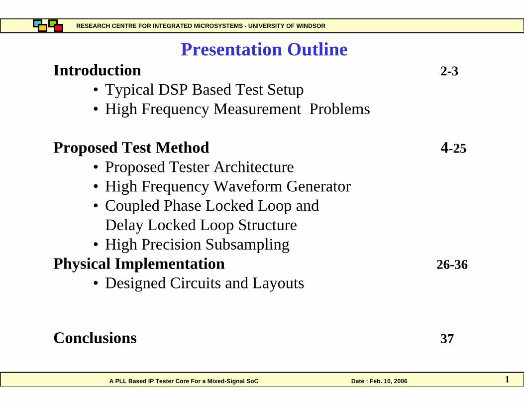
Presentation OutlineIntroduction 2-3
• Typical DSP Based Test Setup • High Frequency Measurement Problems
Proposed Test Method 4-25• Proposed Tester Architecture • High Frequency Waveform Generator • Coupled Phase Locked Loop and
Delay Locked Loop Structure• High Precision Subsampling
Physical Implementation 26-36• Designed Circuits and Layouts
Conclusions 37

A PLL Based IP Tester Core For a Mixed-Signal SoC Date : Feb. 10, 2006
RESEARCH CENTRE FOR INTEGRATED MICROSYSTEMS - UNIVERSITY OF WINDSOR
Typical DSP Based Test Setup for Testing Analog Cores
2
Generate test stimuli by an AWG, apply it to the CUT and capture the response through an ADC
Circuit Under Test ADC
WaveformCapture Memory
ArbitraryWaveformGenerator
Synchronizer
Digital Controller & Processors
A PLL Based IP Tester Core For a Mixed-Signal SoC Date : Feb. 10, 2006
RESEARCH CENTRE FOR INTEGRATED MICROSYSTEMS - UNIVERSITY OF WINDSOR
3
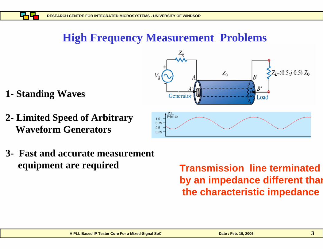
High Frequency Measurement Problems
Transmission line terminated by an impedance different thanthe characteristic impedance
1- Standing Waves
2- Limited Speed of Arbitrary Waveform Generators
3- Fast and accurate measurement equipment are required
A PLL Based IP Tester Core For a Mixed-Signal SoC Date : Feb. 10, 2006
RESEARCH CENTRE FOR INTEGRATED MICROSYSTEMS - UNIVERSITY OF WINDSOR
4
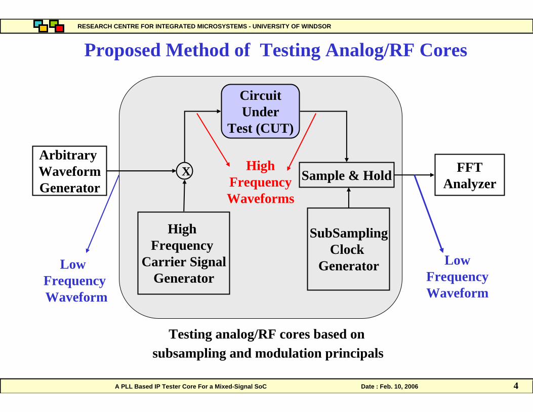
Arbitrary WaveformGenerator
SubSamplingClock
Generator
FFTAnalyzer
CircuitUnder
Test (CUT)
X
High Frequency
Carrier SignalGenerator
Proposed Method of Testing Analog/RF Cores
Testing analog/RF cores based on subsampling and modulation principals
Low FrequencyWaveform
Low FrequencyWaveform
HighFrequencyWaveforms
Sample & Hold

A PLL Based IP Tester Core For a Mixed-Signal SoC Date : Feb. 10, 2006
RESEARCH CENTRE FOR INTEGRATED MICROSYSTEMS - UNIVERSITY OF WINDSOR
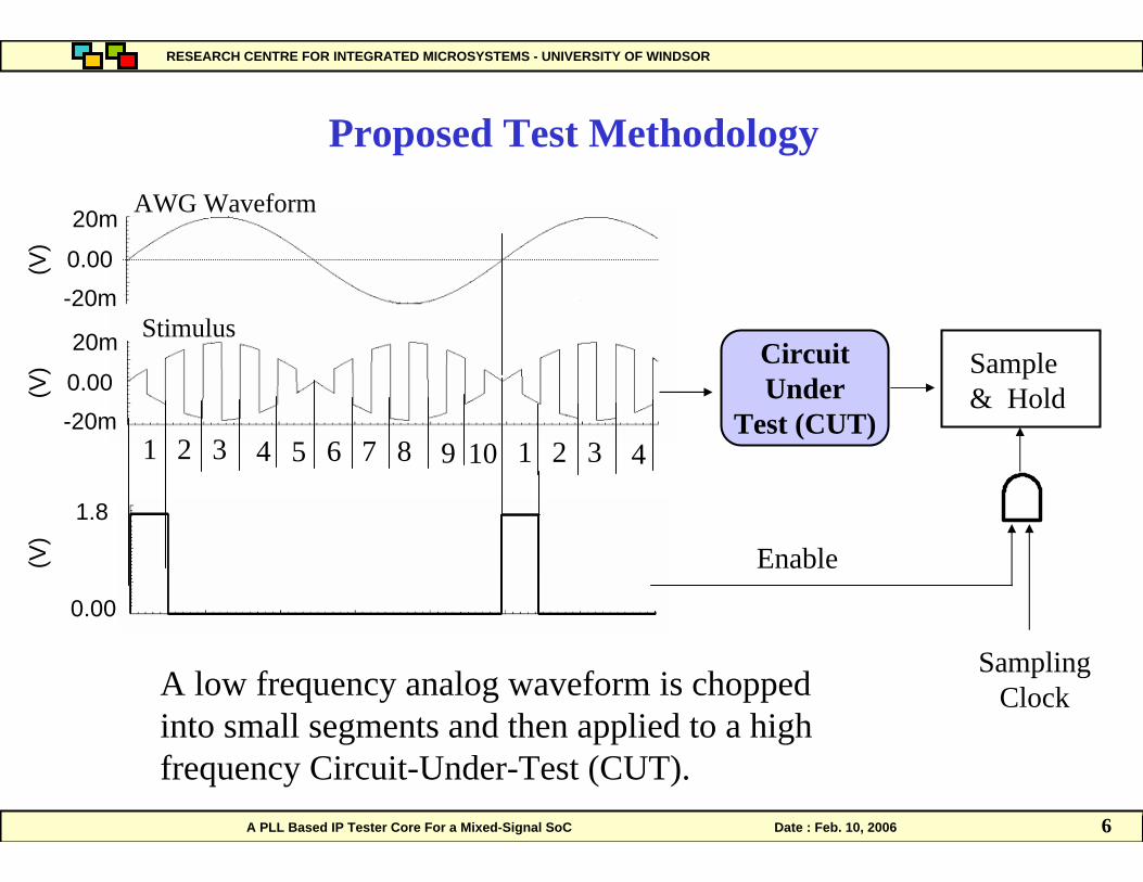
Proposed Test Methodology
CircuitUnder
Test (CUT)
S/H
Subsampling
• A low frequency analog waveform is transferred to high frequency through a chopped modulator and into small segments and then applied to the Circuit_Under_Test (CUT).
1. A High frequency CUT response is transferred to low frequency through subsampling techniques
5
A PLL Based IP Tester Core For a Mixed-Signal SoC Date : Feb. 10, 2006
RESEARCH CENTRE FOR INTEGRATED MICROSYSTEMS - UNIVERSITY OF WINDSOR
20m
-20m0.00(V
)
Stimulus
1 2 543 6 7 1098
20m
-20m0.00(V
)
1 2 43
CircuitUnder
Test (CUT)
Sample & Hold
Enable
SamplingClock
AWG Waveform
1.8
0.00
(V)
Proposed Test Methodology
A low frequency analog waveform is chopped into small segments and then applied to a high frequency Circuit-Under-Test (CUT).
6

A PLL Based IP Tester Core For a Mixed-Signal SoC Date : Feb. 10, 2006
RESEARCH CENTRE FOR INTEGRATED MICROSYSTEMS - UNIVERSITY OF WINDSOR
1
-1
2/sT
x)(tx )(ty)(ts
t
sT
0 2.0n 4.0n 6.0n 8.0n 10.0n 12.0n 14.0n
900m
-900m
0.00
20m
-20m
0.00(V)
(V)
Stimulus
AWG Waveform
Carrier
Time (s)
20m
-20m
0.00(V)
.....5cos)(543cos)(
34cos)(4)( −+−= twtxtwtxtwtxty sss πππ
)(tx
High Frequency Waveform Generator
7

A PLL Based IP Tester Core For a Mixed-Signal SoC Date : Feb. 10, 2006
RESEARCH CENTRE FOR INTEGRATED MICROSYSTEMS - UNIVERSITY OF WINDSOR
PLL Based High Frequency Waveform Generator
CP/LPFPFD
xAWG
Divide by N Counter
VCOClock
Sync. output
Low Frequency Analog Waveform
Carry
Phase Locked Loop
8

A PLL Based IP Tester Core For a Mixed-Signal SoC Date : Feb. 10, 2006
RESEARCH CENTRE FOR INTEGRATED MICROSYSTEMS - UNIVERSITY OF WINDSOR
Implemented High Frequency Waveform Generator
CP/LPF
Multiplexer
PFD
xAWG
Divide by N Counter
VCO
Sel_A
Car
rier
Desired Segment Address
Clock+-
1 6
+-
2 7
+-
3 8
+-
4 9
+-
5 10
1 2 3 54
Sync. output
Low Frequency Analog Waveform
Enable
High Frequency Stimulus
Segment Identifier
A
BA=B
9

A PLL Based IP Tester Core For a Mixed-Signal SoC Date : Feb. 10, 2006
RESEARCH CENTRE FOR INTEGRATED MICROSYSTEMS - UNIVERSITY OF WINDSOR
High Frequency Waveform Generator
CircuitUnder
Test (CUT)
S/H
SubsamplingModuleCP/LPF
Multiplexer
PFD
xAWG
Divide by N
VCO
Sel_A
Segment Identifier
Carr i
er
Desired Segment Address
Clock+-
1 6
+-
2 7
+-
3 8
+-
4 9
+-
5 10
1 2 3 54
Sync.outpu t
Low Frequency Analog Waveform
Enable
High Frequency Stimulus
10

A PLL Based IP Tester Core For a Mixed-Signal SoC Date : Feb. 10, 2006
RESEARCH CENTRE FOR INTEGRATED MICROSYSTEMS - UNIVERSITY OF WINDSOR
Voltage Controlled Oscillator (VCO)
10Tvco
10Tvco
10Tvco
Tvco/2M
1 2 3 M-1 M
pTpT
vcoTpvco TT 2=
cntV
cntV
cntV+-
+-
+-
+-
VCO
+-
1 5432
A single symmetrical delay line can be usedto provide precise timing signals.
11

A PLL Based IP Tester Core For a Mixed-Signal SoC Date : Feb. 10, 2006
RESEARCH CENTRE FOR INTEGRATED MICROSYSTEMS - UNIVERSITY OF WINDSOR
10Tvco
10Tvco
10Tvco
cntV+-
+-
+-
+-
VCO
+-
1 5432
1Φ
2Φ
3Φ
10Φ
10vcoT
102 vcoT
109 vcoT
VCOT
10/VCOT
Voltage Controlled Oscillator (VCO)
12

A PLL Based IP Tester Core For a Mixed-Signal SoC Date : Feb. 10, 2006
RESEARCH CENTRE FOR INTEGRATED MICROSYSTEMS - UNIVERSITY OF WINDSOR
1Φ
2Φ
3Φ
10Φ
VCOT
10/VCOT
1Φ
2Φ
3Φ
11Φ
VCOT
11/VCOT
CP/LPFPFDClock+-
+-
+-
+-
PFD CP/LPF
+-
+-
+-
+-
Tvco/M
Tvco/N
Tvco/M – Tvco/N
VCO
VCDL
1 2 M
1 2 N
When the VCO oscillates at1.01 GHz (Tvco=990ps)
psTVCO 9910/ =
psTVCO 9011/ =
psTT VCOVCO 911/10/ =−
Tvco=990ps
9ps
99ps
90ps
Coupled Phase Locked Loop and Delay Locked Loop Structure
13

A PLL Based IP Tester Core For a Mixed-Signal SoC Date : Feb. 10, 2006
RESEARCH CENTRE FOR INTEGRATED MICROSYSTEMS - UNIVERSITY OF WINDSOR
Subsampling
14
t
Original Waveform Sampled Waveform
tSampleClock
O r ig in a l W ave f o r m
S am p le d W a ve f o r m
f
f
0
yfyf− 0 sf sf2sf−sf2−
xf− xfxff
txty∆
=
=
α
α )()(
A PLL Based IP Tester Core For a Mixed-Signal SoC Date : Feb. 10, 2006
RESEARCH CENTRE FOR INTEGRATED MICROSYSTEMS - UNIVERSITY OF WINDSOR
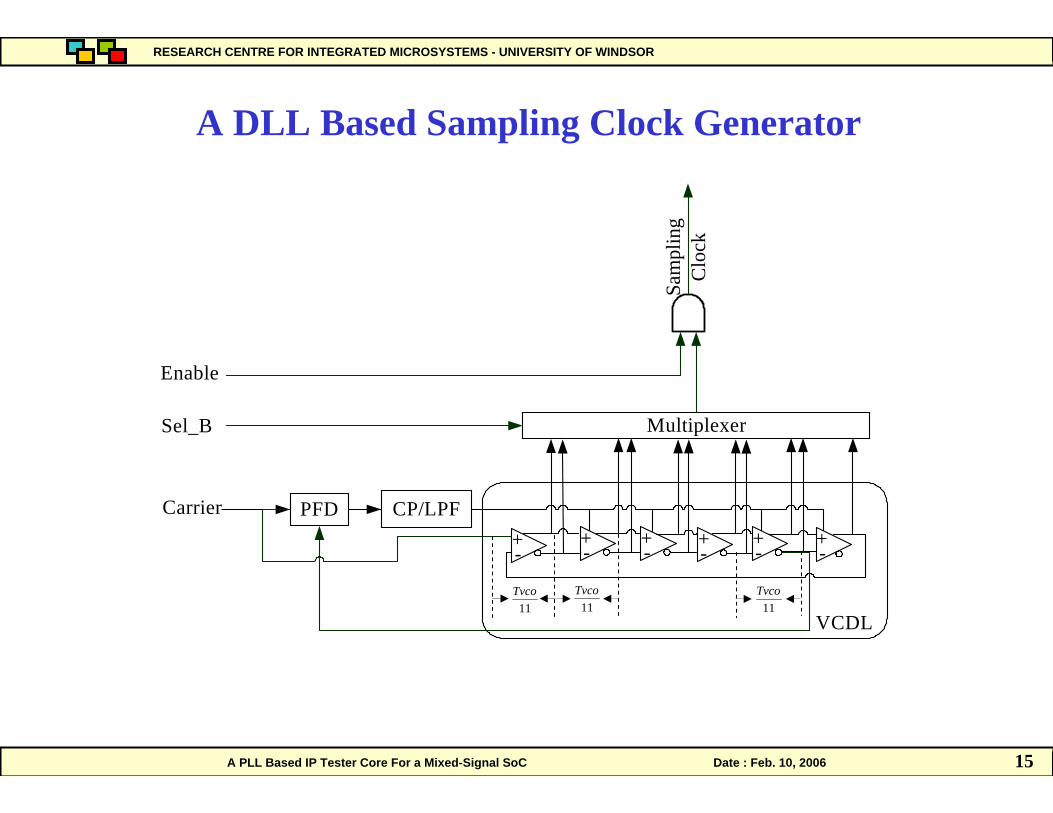
A DLL Based Sampling Clock Generator
CP/LPF
Multiplexer
PFDCarrier+-
+-
+-
+-
VCDL
Sam
plin
g C
lock
+-
+-
Sel_B
Enable
11Tvco
11Tvco
11Tvco
15

A PLL Based IP Tester Core For a Mixed-Signal SoC Date : Feb. 10, 2006
RESEARCH CENTRE FOR INTEGRATED MICROSYSTEMS - UNIVERSITY OF WINDSOR
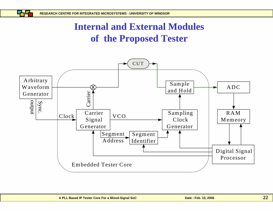
Figure 2. Block Diagram of the Proposed Tester Core
Proposed Tester Architecture
CP/LPF
Multiplexer
PFD
Circuit Under Test
x Sample & HoledAWG
Divide by N
PFD CP/LPF
Multiplexer
+-
+- +-+-
+-
+-
VCDLVCO
1 2 1097 8
1 4 5
1 5 6
1 2 109 11
Select-A Select-B
Segment Identifier
Car
rier
Enable
Address of Desired Segment
Clock
Output
Sam
plin
g C
lock
16
A PLL Based IP Tester Core For a Mixed-Signal SoC Date : Feb. 10, 2006
RESEARCH CENTRE FOR INTEGRATED MICROSYSTEMS - UNIVERSITY OF WINDSOR
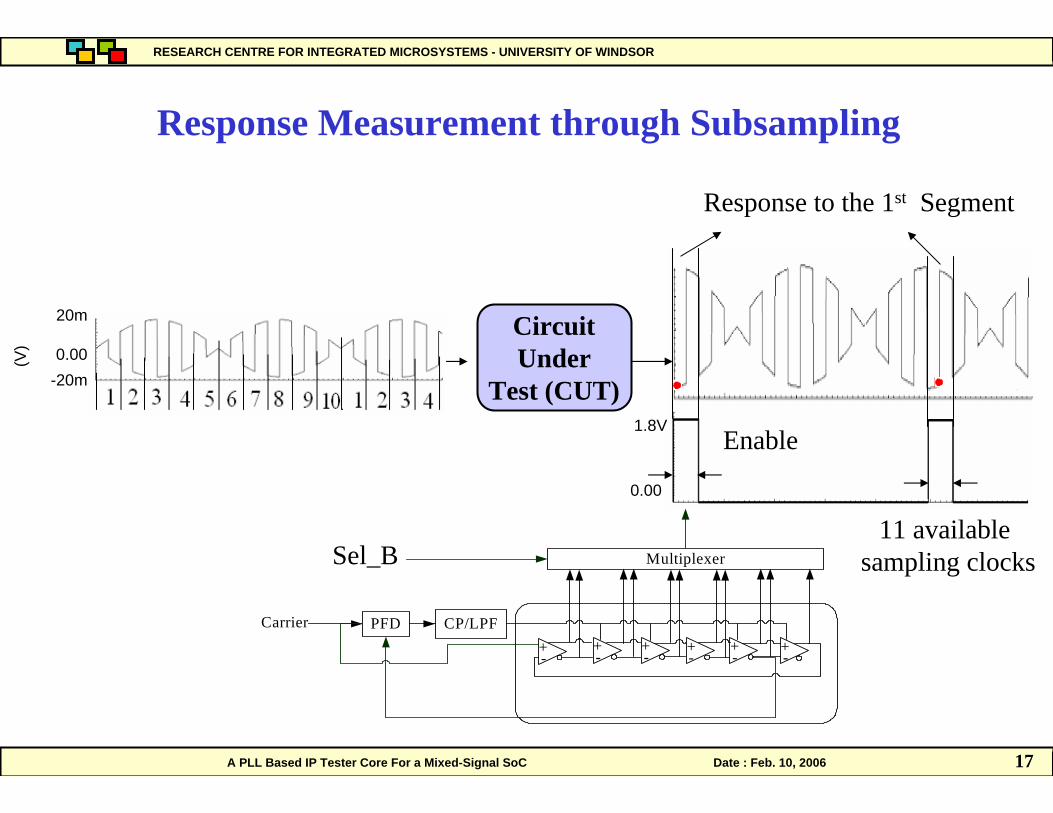
Response Measurement through Subsampling
20m
-20m0.00(V
)
CircuitUnder
Test (CUT)
Enable1.8V
0.00
Response to the 1st Segment
CP/LPF
Multiplexer
PFDCarrier+-
+-
+-
+-
+-
+-
Sel_B11 available
sampling clocks
17

A PLL Based IP Tester Core For a Mixed-Signal SoC Date : Feb. 10, 2006
RESEARCH CENTRE FOR INTEGRATED MICROSYSTEMS - UNIVERSITY OF WINDSOR
1Φ
2Φ
3Φ
10Φ
VCOTVCOT
1Ψ
2Ψ
3Ψ
11Ψ
Multiplexer
Circuit Under Test
x Sample & Holed
MultiplexerSelect-A Select-B
Segment Identifier
Car
rier
Enable
Output
PLL DLL
AnalogWaveform
SegmentAddress
Sync.Output
1Φ
Sync. Output
High Precision Subsampling
PLL Timing Signals DLL Timing Signals
18

A PLL Based IP Tester Core For a Mixed-Signal SoC Date : Feb. 10, 2006
RESEARCH CENTRE FOR INTEGRATED MICROSYSTEMS - UNIVERSITY OF WINDSOR
1Φ
2Φ
3Φ
10Φ
VCOT VCOT
1Ψ
2Ψ
3Ψ
11Ψ
Multiplexer
Circuit Under Test
x Sample & Holed
MultiplexerSelect-A Select-B
Segment Identifier
Car
rier
Enable
Output
PLL DLL
AnalogWaveform
SegmentAddress
Sync.Output
2Φ
Sync. Output
Enable
High Precision Subsampling
PLL Timing Signals DLL Timing Signals
19

A PLL Based IP Tester Core For a Mixed-Signal SoC Date : Feb. 10, 2006
RESEARCH CENTRE FOR INTEGRATED MICROSYSTEMS - UNIVERSITY OF WINDSOR
is selected as a Carrier 1Φ
20m
0.00
900m
-900m
0.00
900m
-900m
0.00
20m
(V)
(V)
(V)
Response Waveform
90ps
90ps
Time (s)
Sampled Instances
990ps
0 400p 800p 1.2n 1.6n 2n
900m
-900m
0.00(V)
900m
-900m
0.00(V)
99ps
90ps
180ps
1Φ
2Φ
1Ψ
2Ψ
Shift and Sample Procedure
20

A PLL Based IP Tester Core For a Mixed-Signal SoC Date : Feb. 10, 2006
RESEARCH CENTRE FOR INTEGRATED MICROSYSTEMS - UNIVERSITY OF WINDSOR
Shift and Sample Procedure
is selected as a Carrier 2Φ
Response Waveform
9ps
81ps
Sampled Instances
990ps
Time (s)0 400p 800p 1.2n 1.6n 2n
20m
0.00
900m
-900m
0.00
900m
-900m
0.00
20m
(V)
(V)
(V)
900m
0.00(V)
900m
-900m
0.00(V)
90ps
-900m
1Φ
2Φ
1Ψ
2Ψ
21
A PLL Based IP Tester Core For a Mixed-Signal SoC Date : Feb. 10, 2006
RESEARCH CENTRE FOR INTEGRATED MICROSYSTEMS - UNIVERSITY OF WINDSOR
CU T
Sam ple and H old
A rbitraryW aveform G enerator
Carrier Signal
G eneratorSegm ent Identifier
D igital Signal Processor
ADC
RAM M em eory
X
Clock
Car
rier
Sam pling Clock
G eneratorSegm entA ddress
Sync. output
V CO
Em bedded Tester Core
Internal and External Modules of the Proposed Tester
22

A PLL Based IP Tester Core For a Mixed-Signal SoC Date : Feb. 10, 2006
RESEARCH CENTRE FOR INTEGRATED MICROSYSTEMS - UNIVERSITY OF WINDSOR
Pow
er (d
Bm
)
Fundamentals
Fundamentals Third Order ModulationDistortion
0.58 dBm
-29.7 dBm
-27.9 dBm
Frequency (GHz)
(a)
(b)
1.991G 1.997G 2.003G 2.009G
1.991G 1.997G 2.003G 2.009G
20.0
00.0
-20.0
-40.0
-60.0
-80.0
-100
-120
Pow
er (d
Bm
)
00.0
-20.0
-40.0
-60.0
-80.0
-100
Two-Sided Power Spectrum of (a) CUT’s Response (b) Applied Stimulus
Testing a Low Noise Amplifier (LNA)
23

A PLL Based IP Tester Core For a Mixed-Signal SoC Date : Feb. 10, 2006
RESEARCH CENTRE FOR INTEGRATED MICROSYSTEMS - UNIVERSITY OF WINDSOR
The Third Order Intermodulation: Circles Represent Simulation Results and Solid Curve Shows Expected Values
Testing a Low Noise Amplifier (LNA)
Input Power (dBm)
IP3
(dB
m)
-30 -27 -24 -21 -18 -15
-6
-8
-10
-12
Measured
Expected
24

A PLL Based IP Tester Core For a Mixed-Signal SoC Date : Feb. 10, 2006
RESEARCH CENTRE FOR INTEGRATED MICROSYSTEMS - UNIVERSITY OF WINDSOR
25
Advantages of the Proposed Test Method
• It enables low speed components to perform test on high speed analog/RF circuits and detect their faults and performance variation.
• The tester has capabilities to reduce the cost of testing by eliminating the need for advanced and costly Automatic Test Equipment (ATE).
Disadvantages• Area overhead• Power overhead
A PLL Based IP Tester Core For a Mixed-Signal SoC Date : Feb. 10, 2006
RESEARCH CENTRE FOR INTEGRATED MICROSYSTEMS - UNIVERSITY OF WINDSOR
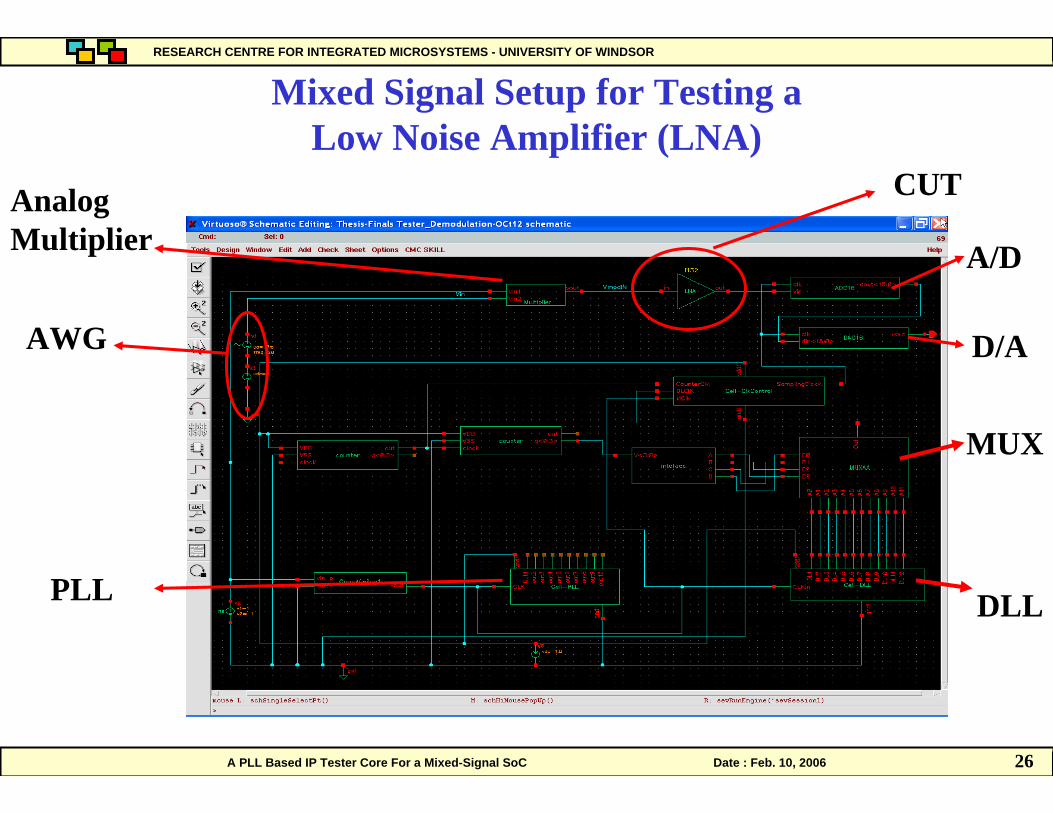
Mixed Signal Setup for Testing a Low Noise Amplifier (LNA)
26
AnalogMultiplier
AWG
PLL DLL
MUX
D/A
A/D
CUT

A PLL Based IP Tester Core For a Mixed-Signal SoC Date : Feb. 10, 2006
RESEARCH CENTRE FOR INTEGRATED MICROSYSTEMS - UNIVERSITY OF WINDSOR
Employed Delay Cell
27
The current of differential pair is linearly controlled by
contVCOout Vkww += 0
contV
psdps t 5020 <<
Controlling Resistance by contV
Reference Current
CurrentMirrors
Input ofNext DelayCell

A PLL Based IP Tester Core For a Mixed-Signal SoC Date : Feb. 10, 2006
RESEARCH CENTRE FOR INTEGRATED MICROSYSTEMS - UNIVERSITY OF WINDSOR
Physical Implementation of Analog Circuits
28
Delay Cell Layout

A PLL Based IP Tester Core For a Mixed-Signal SoC Date : Feb. 10, 2006
RESEARCH CENTRE FOR INTEGRATED MICROSYSTEMS - UNIVERSITY OF WINDSOR
Digital Circuits Physical Implementation
29
Multiplexer
Verilog RTL Codes
Test Bench Codes
Simulation and checking waveforms using “simvision”
Synthesis using “Synopsys” Gate Level Verilog netlist
Add power pins and generate Golden Verilog codes
Import Verilog Golden codes into Cadence Virtuoso Schematic
A PLL Based IP Tester Core For a Mixed-Signal SoC Date : Feb. 10, 2006
RESEARCH CENTRE FOR INTEGRATED MICROSYSTEMS - UNIVERSITY OF WINDSOR
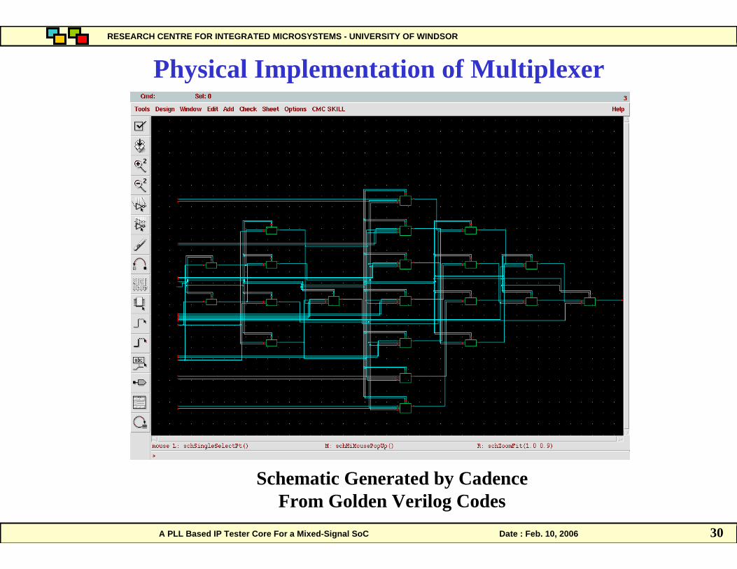
30
Schematic Generated by Cadence From Golden Verilog Codes
Physical Implementation of Multiplexer
A PLL Based IP Tester Core For a Mixed-Signal SoC Date : Feb. 10, 2006
RESEARCH CENTRE FOR INTEGRATED MICROSYSTEMS - UNIVERSITY OF WINDSOR
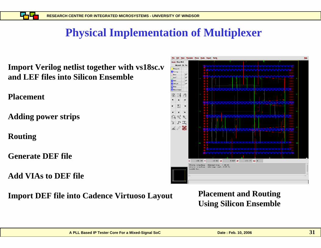
Physical Implementation of Multiplexer
31
Import Verilog netlist together with vs18sc.v and LEF files into Silicon Ensemble
Placement
Adding power strips
Routing
Generate DEF file
Add VIAs to DEF file
Import DEF file into Cadence Virtuoso Layout Placement and RoutingUsing Silicon Ensemble

A PLL Based IP Tester Core For a Mixed-Signal SoC Date : Feb. 10, 2006
RESEARCH CENTRE FOR INTEGRATED MICROSYSTEMS - UNIVERSITY OF WINDSOR
32
Physical Implementation of Multiplexer
Layout Exported to Cadence
DEF filesamended to add VIAsmanually

A PLL Based IP Tester Core For a Mixed-Signal SoC Date : Feb. 10, 2006
RESEARCH CENTRE FOR INTEGRATED MICROSYSTEMS - UNIVERSITY OF WINDSOR
Simulation Results
33
Input, Output and Control Voltage of the Designed PLL

A PLL Based IP Tester Core For a Mixed-Signal SoC Date : Feb. 10, 2006
RESEARCH CENTRE FOR INTEGRATED MICROSYSTEMS - UNIVERSITY OF WINDSOR
Simulation Results
34
Phase Locked Loop
Before Lock After Lock

A PLL Based IP Tester Core For a Mixed-Signal SoC Date : Feb. 10, 2006
RESEARCH CENTRE FOR INTEGRATED MICROSYSTEMS - UNIVERSITY OF WINDSOR
Layout of the Tester Core
35
Coupled PLL &DLL Structure
Chopper Modulator and Sample and Hold Circuitry
Digital Control Circuits
A PLL Based IP Tester Core For a Mixed-Signal SoC Date : Feb. 10, 2006
RESEARCH CENTRE FOR INTEGRATED MICROSYSTEMS - UNIVERSITY OF WINDSOR
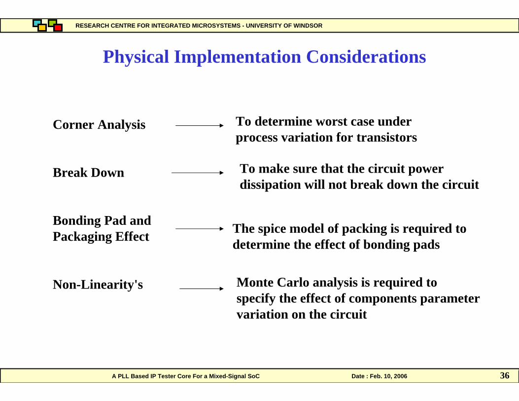
Physical Implementation Considerations
36
Corner Analysis
Break Down
Bonding Pad and Packaging Effect
Non-Linearity's
To determine worst case under process variation for transistors
To make sure that the circuit power dissipation will not break down the circuit
The spice model of packing is required to determine the effect of bonding pads
Monte Carlo analysis is required to specify the effect of components parameter variation on the circuit

A PLL Based IP Tester Core For a Mixed-Signal SoC Date : Feb. 10, 2006
RESEARCH CENTRE FOR INTEGRATED MICROSYSTEMS - UNIVERSITY OF WINDSOR
37
• A novel Analog/RF core tester scheme based on a phase locked loop for mixed signal System-on-Chip (SoC) was presented
• System level simulation, circuit and layout level implementationof the tester using cadence tools were shown
• Simulation results shows the effectiveness of the proposed test methods
Conclusions