a polarity-induced defect mechanism for conductivity and
TRANSCRIPT

1
A polarity-induced defect mechanism for conductivity and magnetism at polar-nonpolar oxide interfaces
Liping Yu and Alex Zunger University of Colorado, Boulder, Colorado 80309, USA
The discovery of conducting two-‐dimensional electron gas (2DEG) and magnetism at the interface between insulating nonmagnetic oxides, as exemplified by the polar LaAlO3 and nonpolar SrTiO3 has raised prospects for attaining interfacial functionalities absent in the component materials. Yet, the microscopic origin of such emergent phenomena remains unclear, posing obstacles to design of improved functionalities. Using first principles defect calculations, we reveal a unifying polarity-‐induced defect mechanism for both conductivity and magnetism at polar-‐nonpolar interfaces of nonmagnetic insulating oxides. We demonstrate that the polar-‐discontinuity across the interface triggers thermodynamically the spontaneous formation of certain defects that in turn cancel the polar field induced by the polar discontinuity. It turns out that the 2DEG originates from those spontaneously formed surface donor defects (oxygen vacancy), but the density of 2DEG is controlled by the interfacial anti-‐site acceptor defects (Al-‐on-‐Ti). The interface magnetism is found to originate from the un-‐ionized deep Ti-‐on-‐Al anti-‐site donor defects within the LaAlO3 side near the interface. Our results suggest practical design guidelines for inducing and controlling both 2DEG and magnetism at polar-‐nonpolar oxide interfaces.
Oxide interfaces exhibit many spectacular phenomena not found in the respective bulk components or in conventional semiconductor interfaces1, providing new avenues for electronics2. The LaAlO3/SrTiO3 interface is a paradigm example, exhibiting conducting 2DEG3,4 and magnetism5-11 between two insulating nonmagnetic metal-oxides. In the [001] direction, two different interfaces can be formed between polar LaAlO3, which consists of alternating LaO)+-(AlO2)- layers, and nonpolar SrTiO3, which consists of alternating (SrO)0-(TiO2)0 layers. One is called n-type (i.e., LaO/TiO2) and the other is called p-type (i.e., AlO2/SrO). The remarkable feature is that the conductivity occurs only at n-type interfaces when the LaAlO3 film thickness (nLAO) is larger than three unit cells (uc)4,5, whereas the magnetism has been observed both at n-type interfaces with nLAO > ~3 uc and at insulating p-type interfaces8. As listed in Table 1, this feature and other experimental observations represent the main puzzles12 that need to be resolved before the promised applications can be realized13.
Existing explanations: At present, no single mechanism can fully explain the vast and growing body of experimental work on this LaAlO3/SrTiO3 system. For 2DEG at n-type interfaces, four main mechanisms have been suggested. The prevalent one is intrinsic electronic reconstruction (so called polar catastrophe) involving ionization of the host valence band of LaAlO3 within the abrupt and defect-free interfaces3,4. The other three mechanisms involve various defects, including the oxygen vacancies at the interface (denoted as VO(I), where “I” means Interface)14-
16, oxygen vacancies at LaAlO3 overlayer surface (denoted as VO(S), where S means Surface )17-
22, and the La-on-Sr (LaSr) antisite donor defects induced by interfacial cation intermixing23-29. As Table 1 shows, each mechanism represents one aspect of the interface physics, explains some experimental findings, but conflicts with a few others2. None explains the insulating nature of p-type interfaces. For interface magnetism, it was shown experimentally that the local magnetic moments are associated with Ti3+ ions5-11,30. However, it is yet unclear whether such Ti3+ ions reside in SrTiO3, or LaAlO3, or both near the interface. Theoretically, it has been postulated that Ti3+ ions arise in SrTiO3 side, involving the occupation of the low-energy Ti-dxy-like sub-bands caused by the interfacial splitting of orbital degeneracy31, or interfacial
2
disorder32,33, or interfacial oxygen vacancies34, which are difficult to reconcile why the magnetism appears at insulating p-type interfaces and at n-type interfaces with a critical thickness (Lc) similar to that for 2DEG.
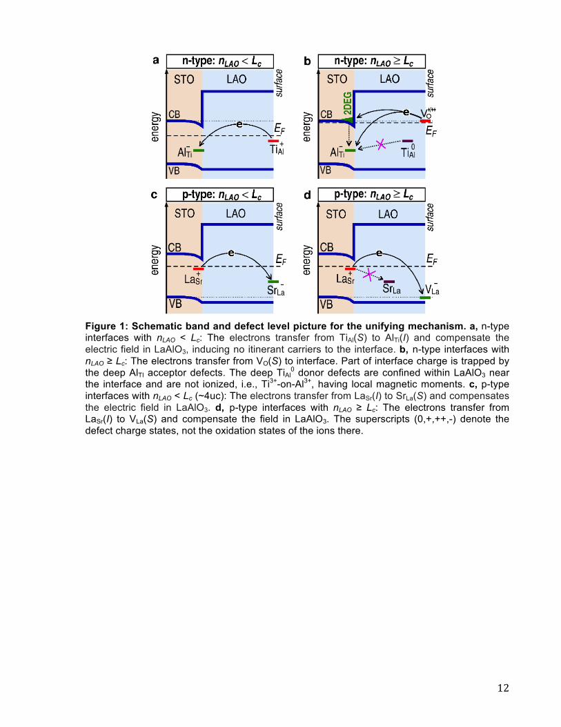
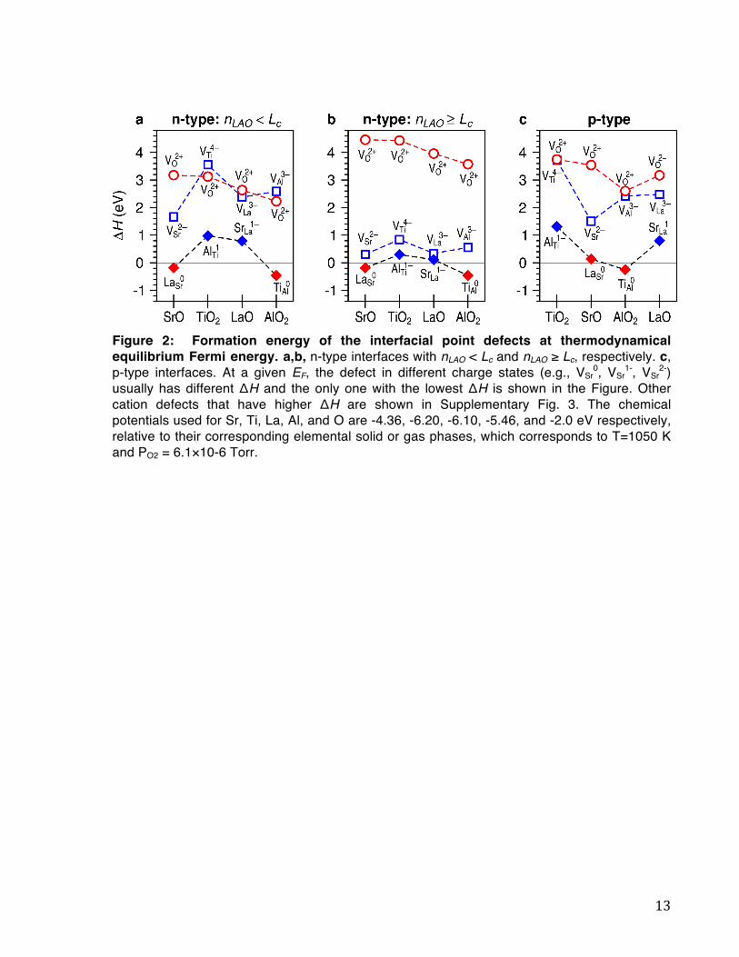
Overarching unresolved questions: a crucial issue associated with the emergent conductivity and magnetism at polar-nonpolar interfaces is what mitigates the divergence of electrostatic potential as the thickness of the polar film increases35. Is it electronic reconstruction within polar catastrophe scenario, atomic reconstruction, or chemical defects? Different answer represents different mechanism, suggesting different controlling parameters. It has been purported that all these three effects exist to varying degrees in real materials and contribute to the emergent interface phenomena. However, whether and how these effects are physically connected, and what are their relative contributions, remain uncertain. Particularly, for defects, it is unclear which specific defects can be induced and are responsible for the emergent interface phenomena. Using first principles electronic and defect calculations, we identify the specific defects that can form spontaneously as a response to the built-in polar field and show how these defects lead to a unifying mechanism (Figure 1) that simultaneously explains the main features of both conductivity and magnetism at the interface. The key physical quantities that feature in our explanation are (i) the formation energy ΔH (which controls the defect concentration) (Figure 2) of the defect in various charge states at thermodynamic equilibrium Fermi-energy EF, and (ii) the donor or acceptor electrical levels (Figure 3), i.e., the defect charge transition energy ε(q/qʹ′) defined as the EF where the ΔH of a defect at two different charge states q and qʹ′ equal. A donor can produce electrons and compensate holes, whereas an acceptor can produce holes and compensate electrons. These two quantities (i) and (ii) have not been previously calculated for charged defects in different layers across the interfaces and turn out to be crucial. The details of their first principles calculations are given in Methods section.
The central point of the proposed mechanism is that the polar-discontinuity induced built-in polar field triggers thermodynamically the spontaneous formation of the certain defects at surface and/or interface, which in turn compensate the built-in polar field and thus avoids the potential divergence. Thus, it is the polar-field induced defects, rather than the electronic or atomic reconstruction, that are responsible for the conductivity and magnetism at the interface. Specifically, we find that the surface donor defect (here VO) has its donor levels located energetically above the SrTiO3 conduction band at the interface but below the LaAlO3 conduction band. This donor level position is a prerequisite for 2DEG formation. Although the 2DEG owes its existence to the surface donors, the density of 2DEG is controlled by the interfacial deep acceptor defects (mainly Al-on-Ti antisite). It is also turn out that the interface magnetic moment is caused by the unionized deep Ti-on-Al antisite defects located within the LaAlO3 side near the interface.
In what follows we address specifically how this polar-field induced defect mechanism resolves the long-standing puzzles on the origin of 2DEG, the critical thickness for 2DEG, the weak field in LaAlO3 film, the density of 2DEG, the insulating p-type interfaces, and the origin of the local magnetism moments. During this process, we also distill the general rules that control the pertinent effects and allow future section of other polar-nonpolar interface materials with similar or improved interface properties.
1. What creates the 2DEG?
3
The 2DEG is unlikely to originate from the defect-free scenarios: these include the ionization of the intrinsic LaAlO3 valence bands (suggested by the polar catastrophe model3,4) or the ionization of the LaO interface layer (suggested by the interfacial charge leaking model)36 (Supplementary note 1). This is simply because that the creation of 2DEG in these defect-free scenarios requires the LaAlO3 valence band maximum (VBM) to cross the SrTiO3 conduction band minimum (CBM) or Fermi-energy EF. This is contrary to the experimentally observed weak field (negligible band-bending)37-40 in the LaAlO3 film, clearly showing that the LaAlO3 VBM is far below the EF.
The 2DEG also is unlikely to originate from interfacial point donor defects (LaSr, TiAl, and VO). Recall first that the defect formation energy ΔH depends on the EF (or chemical potential) and the defect charge transition energy ε(q/qʹ′) needs to be close to band edges in order to producing free carriers. In thermodynamic equilibrium, the EF of the system pins around the middle of SrTiO3 band gap when nLAO < Lc, and around the SrTiO3 conduction band edge near the interface when nLAO ≥ Lc (Supplementary note 2). In either case, Fig.2ab shows that the ΔH of the anti-site donor defects, LaSr
0 and TiAl0 is small positive or even negative (note: the
superscript denotes the defect charge states, not the nominal oxidation state of the atom at the defect site). In other words, the formation of such antisite defects at the thermodynamic equilibrium EF is energetically favorable and would inevitably lead to interfacial cation mixing. However, at such EF, both LaSr
0 and TiAl0 defects are stable in their charge neutral states (as
indicated by the superscript), contributing no free carriers. On the other hand, the interfacial VO defects are energetically stable in the charged states, i.e., VO
2+ (Fig.2ab). This means that if formed, the VO will donate electrons and thereby become positively charged. However, the ΔH of VO
2+ at such equilibrium EF is rather high (> 2.5eV), implying that VO2+ have very low
concentration under thermodynamic equilibrium conditions. The high ΔH also means that even if the VO defects are formed under non-equilibrium growth conditions, they can still be removed easily by the post O-rich annealing process41 (Supplementary note 3). Thus, contrary to earlier postulations, these interfacial donor defects are not responsible for 2DEG, consistent with recent experiments42.
The oxygen vacancy, VO(S), at the free LaAlO3 surface can explain the interfacial 2DEG. For this to happen, three conditions (“design principles”) need to be satisfied. First, VO(S) in the polar film material needs to have a sufficiently low formation energy ΔH so it could form. Fig.4a shows the ΔH of VO(S) decreases linearly as the film thickness nLAO increases, consistent with previous calculations20,43. When nLAO ≥ 3-4 uc, the ΔH becomes zero or negative, and VO(S) will form spontaneously and be stable even for high oxygen chemical potentials. (This suggests that even exposing the surface to air or post-annealing under O-rich environment cannot heal these vacancies). Second, the donor transition level of VO(S) in the polar film material should be higher in energy than the substrate (SrTiO3 ) conduction band edge at the interface. Fig.3 shows that this condition is also satisfied. Third, the system needs to have a none-zero built-in polar field that would enable the electron to transfer from the surface to the interface. Such transfer sets up an opposite dipole (proportional to nLAO), which in turn cancels the field and lowers the ΔH. The larger the nLAO, the lower the ΔH. Note that in the absence of such field, the surface-to-interface charge transfer would not occur since such a transfer would create a dipole that would increase the electrostatic energy (proportional to that dipole) and thus raise the total energy of the system. These three conditions are satisfied in this LaAlO3/SrTiO3 system. It is important to note that the built-in polar field always exists during the layer-by-layer growth. This is because that the surface defects (here VO) can cancel the built-in polar field only

4
in the LaAlO3 film between the interface and the surface, not the built-in polar field in the LaAlO3 film to be grown on top of the surface. Such polar field can then always trigger VO formation at the surface of LaAlO3 film to be grown, no matter whether the polar field has been cancelled in the LaAlO3 substrate or not. The emerging picture for the formation of the 2DEG is that the electrons ionized from VO(S) of the polar film material transfer to the nonpolar substrate material SrTiO3 conduction bands at the interface via the built-in polar field, thus forming the 2DEG at that interface. This charge transfer in turn cancels the built-in polar field in LaAlO3. After the built-in field has been cancelled, the ΔH of VO(S) return to a high value (> 3 eV) characteristic of the bulk, and VO(S) become again hard to form in thermodynamic equilibrium20. Thus, the maximum concentration of VO(S) is 0.25/S2D (where S2D is 2D unit cell area), i.e., one of eight oxygen missing at surface, donating 0.5 e/S2D that cancels the polar field in LaAlO3 completely. The compensation of polar field by VO(S) also means that the band bending in LaAlO3 due to polar field is also removed. Thus, the LaAlO3 valence bands fall well below the EF, contrary to what the polar catastrophe model would suggest. Consequently, no free holes can arise from depopulation of the LaAlO3 valence bands at the surface, consistent with experiments3,22.
The emerging design principles for selecting materials that will likely form interface 2DEG: (i) the nonpolar material has a conduction band minimum (CBM) sitting in the band gap of the polar material; (ii) The polar material has at least one deep donor defect with its donor level higher than the conduction band of the nonpolar material at the interface. The (i) and (ii) in together guarantee that the 2DEG forms only at the n-type interfaces. This picture suggests that the 2DEG at n-type LaAlO3/SrTiO3 interfaces may also be induced and/or tuned by using some surface adsorbates (e.g., H2O, H)44-46 or metallic contacts47 provided that the ionization energy of the surface adsorbate or the metallic contact is not lower than the donor level of the VO(S).
2. What controls the critical thickness? The linear decrease of ΔH of VO(S) with increasing polar film thickness nLAO naturally explains the critical thickness Lc for the metal-insulator transition. The rate of decrease (i.e., the slope dΔH/dnLAO) equals 0.19 eV/Å, which is same as the calculated built-in polar field in the defect-free LaAlO3 film (Supplementary note 4). The VO(S) defects start to form spontaneously when the ΔH becomes zero at an Lc of ~4 uc under a typical O-rich growth condition (Fig.3a). For the LaAlO3 film that is one unit cell thinner than this Lc, the calculated ΔH of VO(S) is 0.75 eV, which is too high to produce significant free carrier concentration. Thus, the appearance of VO(S) (and the ensuing metal-insulator transition) at Lc is predicted to be sharp, distinct from the gradual appearance of 2DEG behavior as predicted from polar catastrophe model, but consistent with experiments48.
Fig.3a suggests that the Lc resulting from VO(S) is controlled by the formation energy ΔHo of VO at interface (or the ΔH extrapolated at nLAO =0) and the polar field Ep via Lc = ΔHo/eEp. Since Ep=4πP0/! (where ! and P0 are the dielectric constant and formal polarization of LaAlO3 film), this relation can be written as Lc = ΔHo!/4πeP0, which predicts an Lc of ~4 uc, depending slightly on the O-poor/rich growth conditions (Supplementary note 5). The relation of Lc = ΔHo!/4πeP0 provides an alternative explanation for the observed variation of the Lc with the fraction x in (LaAlO3)1-x(SrTiO3)x overlayer (where P0 is proportional to x)49. This observation was originally explained by Lc = ΔΦ!/4πeP0 (where ΔΦ is the energy difference between LaAlO3 VBM and SrTiO3 CBM) within polar catastrophe model49. Since ΔΦ and ΔHo have
5
similar value (~3-4 eV), it is not surprising that the Lc predicted from these two models is also similar. Implication on the design of carrier mobility: (i) The relatively high 2DEG mobility may be enabled by a modulated doping effect50, whereby the source of carriers (here at the LaAlO3 surface) is spatially separated from the place where the carriers reside (here at the LaAlO3/SrTiO3 interface), thus minimizing carrier scattering by the defects. This minimal spatial separation is measured by the critical thickness Lc. The relationship Lc = ΔHo!/4πeP0 suggests that a large Lc (hence maintaining good mobility) could be achieved by selecting a polar materials with small polarization, large dielectric constant, and donor defects characterized by high formation energy ΔH at the interface or in the bulk. On the other hand, (ii) the concentration of interfacial defects should be minimized in order to take advantage of (i). In addition, (iii) since the 2DEG is located at the conduction bands of the nonpolar material, it is advantageous to select the nonpolar material with low electron effective mass in order to achiever higher mobility.
3. What compensates the built-in polar field? Experimentally, only very weak residual field has been observed in the LaAlO3 film no matter whether its thickness is below or above the Lc
37-40. This observation cannot be explained within the defect-free interface scenario. In turn, whereas the VO(S) model explains the weak electric field in LaAlO3 film above the Lc, it does not explain it below the Lc. This leads us to inspect the effects of all possible cation antisite defects across the interface. In term of point defect, each interfacial antisite alone cannot cancel the polar field. Fig.2ab shows that the LaSr, SrLa, TiAl, and AlTi antisite defects have lower ΔH than other point defects (e.g., vacancy) in the layer where they are located. This means that these four antisite defects are the dominating defects in their corresponding layers. Apparently, the interfacial LaSr donor in SrTiO3 side cannot set up an opposite dipole across the LaAlO3 film that can cancel the polar field inside the LaAlO3 film. For the TiAl donor in LaAlO3 side, since its donor level is lower than the SrTiO3 conduction band at the interface, the ionized electrons cannot be transferred to the latter either to cancel the polar field. For interfacial AlTi and SrLa acceptors, the polar field compensation is similar to that in polar catastrophe model: before the LaAlO3 VBM reaches the acceptor levels of AlTi or SrLa, the polar field cannot be cancelled; After that, the electrons start to transfer from LaAlO3 valence bands to the acceptor levels of these defects, and the internal field decreases gradually as nLAO increase, approaching zero at infinitely large nLAO.
The [TiAl+AlTi] defect pair is the most potent source of polar field cancellation among those donor-acceptor antisite defect pairs at n-type interfaces. The four leading antisite defects can form four types of donor–acceptor pairs: [TiAl+AlTi], [LaSr+SrLa], [LaSr+AlTi], and [TiAl+SrLa], which are denoted as �,�,�,� respectively in Fig.3. Clearly, the electron-transfer from donor to acceptor in both pair � and � is unlikely since it will create a dipole in the same direction as the intrinsic dipole in LaAlO3, and thus increase the dipole moment (also the electrostatic energy) and destabilize the interface. In both pair � and �, the charge transfer can cancel the polar field. However, the electron transfer in pair � is energetically much more favorable because (i) AlTi has a lower acceptor level than SrLa and (ii) the donor-acceptor separation distance (also the associated opposite dipole moment that lowers the total energy of the system) is larger in pair � (Fig.3a).
For nLAO < Lc, the [AlTi+TiAl] can form spontaneously via Ti⇔Al exchange across the interface and cancel the polar field. Fig.4b (filled symbols) shows that the energy required to

6
form such defect pair is negative (i.e., exothermic), and the largest energy gain is obtained when a Ti atom of TiO2-interface monolayer is exchanged with an Al of AlO2-surface monolayer, i.e., AlTi(I)+TiAl(S), which is consistent with previous first-principles calculations51. This means that Ti atom at the interface would hop to the AlO2 surface layer and exchange with Al atom there. Similar to that of VO(S), the linear decrease of ΔH with increasing donor-acceptor separating distance (Fig.4b) is a sign of polar field compensation by electron transfer from TiAl donor to AlTi acceptor, which is expected since the donor level is higher than acceptor level (Fig.3a). Fig.4a also shows that the VO(S) has too high ΔH to form for nLAO < Lc (Fig.4a). Therefore, the polar field is cancelled by those spontaneously formed [AlTi(I)+TiAl(S)] pairs. On the other hand, since these defects are deep, they cannot cause free carriers in the both interface and surface regions (whence insulating). For nLAO ≥ Lc, the polar field is cancelled by spontaneously formed VO(S), not by [AlTi(I)+TiAl(S)]. Recall that the polar field always exists in the LaAlO3 layers during the lay-by-layer growth. The existence of this polar field can always trigger the formation of VO(S) and/or TiAl(S) defects as nLAO increases. For nLAO ≥ Lc, both VO(S) (Fig.4a) and [AlTi(I)+TiAl(S)] pair (Fig.4b) have zero or negative ΔH, meaning that both could form in ideal interfaces. However, if both VO(S) and TiAl(S) present, since VO has a higher donor level than TiAl (Fig.3a), the electron transfer from VO(S) to AlTi(I) is energetically more favorable than that from TiAl(S) to AlTi(I), and the polar field is thus always cancelled by the former. After the polar field has been cancelled by VO(S), Fig.4b (open symbols) shows that the ΔH of [AlTi(I)+TiAl(S)] pair becomes positive (0.4-0.7 eV), meaning that [TiAl+AlTi] pairs cannot be formed via Ti⇔Al exchange over a distance beyond Lc. Therefore, for nLAO ≥ Lc, only VO(S) defects can form and cancel the polar field.
4. What controls the density of 2DEG? Reinterpretation of the puzzle: According to Gauss’ law, the experimentally observed weak electric field in LaAlO3 film means that the total external charge density (mobile and/or immobile) at the interface must be ~0.5 e/S2D (Supplementary note 6). For nLAO < Lc, not conductivity at interfaces means that all (or almost all) interfacial charge does not contribute to the conductivity. For nLAO ≥ Lc, only a fraction of 0.5 e/S2D interfacial charge is seen in transport and so the majority of 0.5 e/S2D charge does not contribute to the conductivity. The puzzle thus is why the ~0.5 e/S2D charge exists at the interface with any nLAO but only a small part of it contribute to conducting 2DEG when nLAO ≥ Lc. This puzzle cannot be explained within defect-free interface scenario by polar catastrophe model3,4 or interfacial charge leaking model36, since both predict zero interfacial charge for nLAO < Lc and an interfacial charge density much higher than the measured 2DEG density for nLAO ≥ Lc (Supplementary Fig.S1). The possibility of multiple carrier types (i.e., the electrons occupying dxy and those occupying dxz/dyz sub-bands contribute differently in transport) at ideal interfaces has also been suggested to explain the measured 2DEG density above the Lc
52-55. Similarly, the existence of such multiple carrier types could not explain the 0.5 e/S2D interface charge that indeed exists. Moreover, it is also difficult to reconcile why a full carrier density of 0.5 e/S2D has been observed at GdTiO3/SrTiO3 interfaces (where the same multiple carrier types exist)56.
The 2DEG density is controlled by the concentration of immobile acceptor defects that can trap itinerant electrons. Within the emerging defect picture, the total interfacial charge is always ~ 0.5 e/S2D, which corresponds to the (almost) complete polar field cancellation. In SrTiO3 side (where the 2DEG is located), there are mainly three types of acceptor defects, namely, AlTi, VSr, and VTi. At equilibrium EF, Fig.2ab shows that these acceptor defects all
7
prefer to stay in negative charge states, i.e., AlTi1-, VSr
2-, and VTi4-. (In other defect charge states,
these defects have much higher ΔH and are not shown in Fig.2ab). It means that once these defects form they will trap free electrons from the system and get negatively charged. Among these acceptor defects, AlTi
1- acceptors have the lowest ΔH and thus they the most potent electron-trapper. For nLAO < Lc, the AlTi defects resulting from Ti⇔Al exchange trap all free electrons transferred from TiAl(S) defects, and hence no free carrier can occur. For nLAO ≥ Lc, due to VO(S), the ΔH of [TiAl+AlTi] pair changes from negative to positive (Fig.4b), meaning that the concentration of AlTi defect resulting from Ti⇔Al exchange is reduced, compare to that formed below the Lc. Therefore, the AlTi defect concentration is not sufficient to trap all 0.5e/S2D electrons transferred from VO(S). Therefore, only a small fraction of 0.5 e/S2D can contribute to interface 2DEG.
The recently observed LaAlO3 cation-stoichiometry effect on 2DEG formation42 may also be understood within above picture. For Al-rich LaAlO3 film, where both A-site and B-site sublattices are fully occupied (hence having no cation vacancies), the AlTi anti-sites are the only electron-trapping defects and the incomplete trapping of 0.5e/S2D interface charge by AlTi defects leads to interface conductivity. However, for La-rich LaAlO3 film, where B-site sublattice is not fully occupied, the cation vacancies (VTi and VAl) also become main electron-trappers, in addition to AlTi(I). Though, the concentration of AlTi is reduced, each cation vacancy induced in La-rich film traps more electrons than an AlTi. The insulating character can be then attributed to the complete interfacial electron trapping by both interfacial cation vacancies and AlTi (I). The picture of AlTi(I) as main electron-trapping defects may be extended to SrTiO3/GdTiO3 interfaces. The observed full carrier density of 0.5 e/S2D there56 can be ascribed to the fact that both SrTiO3 and GdTiO3 have the same Ti atom at B-site sublattice and have no AlTi-like antisite defects at the interface. Implication on how to increase the density of 2DEG: The above picture suggests that the main controlling factor for the interface carrier density is the concentration of the acceptor defects (mainly AlTi in stoichiometric or Al-rich film), which should be minimized for enhancing carrier density. Such AlTi-like electron trapping defects may be completely removed by designing other oxide interfaces like GdTiO3/SrTiO3 interfaces, whose bulk components have a common cation atom with multiple valence states.
5. Why are the p-type interfaces insulating? The intriguing fact is that the so-called p-type interfaces are not p-type (hole) conducting and are actually insulating. The defect-free polar-catastrophe model for p-type interface predicts a hole conducting interface and an electron conducting surface when nLAO > ~7.3 uc (Supplementary Fig.1) in contradiction with the insulating behavior observed robustly in experiment. To explain this, defects thus be involved. The emerging defect picture below differs from the literature model based solely on interfacial hole-polaron57 or interfacial hole-compensating VO defects23,43, which assumes that the interface has holes arising from the depopulation of the intrinsic SrTiO3 valence bands. Interfacial point defects can neither cause conductivity nor cancel the polar field. Similar to that at n-type interfaces, the interfacial LaSr and TiAr are stable at their charge neutral states and have negligible or negative ΔH at equilibrium EF. It means that they cause inevitable interfacial cation intermixing but induce no free carriers. The VO and other defects at the interface have too high ΔH to form and thus they do not produce free carriers either. Also for similar reason,
8
each leading antisite defect (LaSr, SrLa, TiAl, or AlTi) alone at p-type interfaces cannot cancel the polar field. The spontaneously formed donor-acceptor defect pairs always cancel the polar field but do not induce free carriers. In the p-type interfaces, the polar field points from surface to interface, which is opposite to that in the n-type interfaces. Among four donor-acceptor defect pairs as indicted in Fig.3b, the pair � (i.e., [LaSr+SrLa]) is energetically most favorable in polar field cancellation. For nLAO < ~ 4uc, the [LaSr(I)+SrLa(S)] pairs have negative ΔH (Fig.4d) and can form spontaneously via La⇔Sr exchanges, whereas the [LaSr(I)+VLa(S)] have too high ΔH to form (Fig.4c). So the polar field is cancelled by the charge transfer from LaSr(I) to SrLa(S), which can be expected from their relative defect levels (Fig. 3b) and their linear decreasing behavior in ΔH as a function of nLAO (Fig.4d). For nLAO ≥ ~4uc, the ΔH of [LaSr(I)+VLa(S)] become negative (Fig.4c) and can also form spontaneously. Since VLa has a lower acceptor level than SrLa (Fig.3b), the polar field is cancelled by the charge transfer from LaSr(I) to VLa(S), rather than to SrLa(S). In absence of electric field, Fig.4d (open symbols) indicates that the La⇔Sr exchanges cannot occur anymore over a distance of ~ 4uc. Unlike that in n-type interfaces, the VO(S) defects in p-type interface always have too high ΔH to form. The defects involved in polar field cancellation are all deep. The calculated equilibrium EF according to those point defects turns out to stay always around the middle of SrTiO3 band gap. It means that both VBM and CBM are far away from the EF and there are no free carrier arising from the depopulation of VBM and CBM in both interface and surface regions (whence insulating).
Implication on the design of two-dimensional hole conductivity: Clearly, the formation of interfacial free holes is prevented by these spontaneously formed deep LaSr defects that have donor level higher than the VBM at the interface. So to induce interfacial hole conductivity, one should search for the polar-nonpolar interfaces where all such donors have too high enough formation energy to form or (ii) their donor levels below the VBM at the interface. Practically, the (ii) may be achieved more easily by searching for the polar material whose VBM is higher than the charge transition energy levels of those spontaneously formed interfacial donor defects.
6. What causes interface magnetism? Distinct form previous models31-34 that explain magnetism based on interfacial Ti(3+) within the SrTiO3 (i.e, not a defect), we find below that the local magnetic moment originates from the un-ionized deep TiAl anti site defect (i.e., Ti(3+)-on-Al(3+) within LaAlO3 side near the interface. The interface magnetism depends on the concentration and spatial distribution of such TiAl defects. This picture explains not only why the magnetism appears at n-type interfaces with a similar critical thickness to that for 2DEG, but also why the magnetism also appears at insulating p-type interfaces8. What causes local moment: For n-type interfaces, when nLAO < Lc, the polar field in LaAlO3 is cancelled by the charge transfer from TiAl(S) defects to the interface. These formed TiAl defects are thus ionized, i.e., TiAl
1+ (where superscript denotes the defect charge states). The Ti atom at this defect site has oxidation states of 4+, denoted as, Ti(4+) which has no local magnetic moment. When nLAO ≥ Lc, the polar field in LaAlO3 is cancelled by the charge transfer to the interface from VO(S) instead of TiAl. All TiAl(I) defects in LaAlO3 film in absence of internal field are most stable in their charge neutral (or un-ionized) states, i.e., TiAl
0, where Ti appears as Ti(3+) oxidation state, having a finite local magnetic moment. Therefore, the interface magnetism at n-type interfaces due to those un-ionized TiAl
0 defects should also have a critical thickness of ~4uc. For p-type interfaces, it is the charge transfer among the defects other than

9
TiAl defects that cancels the polar field in in LaAlO3. So all formed TiAl defects there are not ionized, having local magnetic moments, and can cause interface magnetism. The magnitude of local moment: The local moment of a single TiAl defect at the interface can be estimated from that in bulk LaAlO3, which is 0.84µB from our hybrid functional calculation. For ferromagnetic order as observed in experiment, the total interface magnetic moment depends on the concentration of un-ionized TiAl defects in LaAlO3 and can be very small per Ti atom in average. The experimentally observed inhomogeneous landscape of magnetism that also varies from sample to sample8,9 may be attributed to the various spatial distributions of TiAl defects, which may be sensitive to sample preparation conditions (such as temperature and PO2) and local strain. Comparing with VO(I) model: Relative to VO(I) as the origin of local moment, the TiAl(I) defects within LaAlO side are more reasonable in at least two aspects. First, the deep TiAl defect is spatially localized and has an unambiguous local moment. While for VO, which is a shallow donor, it donates electrons to the lower-energy interfacial Ti dxy sub-bands that have light effective mass inside the interface plane55, and the resulting Ti(3+) may then be itinerant. Second, the TiAl defects would form easily or even inevitable due to its small or negative ΔH, whereas the interfacial VO require significant energy to form and if formed they may be removed completely after annealing.
Discussion This work establishes a physical link between polar discontinuity and defect formation: the polar discontinuity triggers spontaneous formation of certain defects that in turn cancel the polar field induced by polar discontinuity. This link reveals a unifying mechanism that simultaneously explains the experimental observations listed in Table 1. This mechanism leads to a set of design rules for both conductivity and magnetism at the LaAlO3/SrTiO3 interfaces and enables the design of other polar-nonpolar interfaces (not limited to oxides) with similar or improved interface properties by first principles defect calculations. Having ruled out the electronic reconstruction, interfacial VO, and interfacial cation intermixing mechanism as the possible origin of 2DEG in our calculations, we conclude that the 2DEG at n-type interfaces with nLAO ≥ Lc originates from the spontaneously formed VO(S) defects. This conclusion stems from the finding that the donor level of deep VO in in LaAlO3 side is higher than the SrTiO3 conduction band edge at the interface. This finding explains why the formation energy of VO(S) decreases linearly as nLAO increases. The linear decreasing relation reveals a general formula and some new controlling parameters for the critical thickness of sharp metal-insulator transition in absence of the electric field in the polar LaAlO3 film. Instead of causing 2DEG, we find that the defects resulting from interfacial cation anti sites play key roles in other aspects. Specifically, (i) the cation intermixing cancels the polar field only below the critical thickness for both-type of interfaces. (ii) the interfacial AlTi acceptor defects control the density of 2DEG. (iii) the un-ionized interfacial TiAl defects within LaAlO3 side cause the local magnetic moments. The (iii) suggests that all previous models on interface magnetism based on Ti(3+) ions in SrTiO3 side should be revisited. Importantly, we find that the cation mixing is confined near the interface and does not extend in LaAlO3 side over more than ~4 uc, above which the cation intermixing is prevented by spontaneous formation of some surface vacancy defects. This spatial confinement is critical for realizing nanoscale interface magnetism.

10
This mechanism provides three distinctive predictions to be tested in experiment as further validation. (i) For n-type interfaces, the AlO2-surface layer is dominated by TiAl defects when nLAO < Lc and by VO defect when nLAO ≥ Lc. (ii) For p-type interfaces, the LaO-surface layer is dominated by SrLa and VLa defects, respectively, below and above an Lc of ~4 uc. (iii) Ti4+ and Ti3+ signals exist in both sides of the interface. The appearance of the Ti3+ signals should not be taken as a sign of conductivity. Whether the Ti3+ signals detected by photoemission below the Lc
21,39,58,59 can be truly assigned to those Ti3+ ions in SrTiO3 side should be revisited carefully. How these TiAl local moments are ordered (ferromagnetic, or antiferromagnetic, or else) and whether and how they interact with the itinerant 2DEG are still open questions that should be investigated further.
Methods All calculations were performed using density functional theory (DFT) and plane-wave projector augmented-wave (PAW)60 method as implemented in the VASP code61. An energy cutoff of 400 eV was used. The Brillouin zone was sampled by 8 ✕ 8 ✕ 1 and 4 ✕ 4 ✕ 1 k-point mesh for 1 ✕ 1 and 2 ✕ 2 in-plane supercell respectively. The atomic forces were relaxed to be less than 0.03 eV/Å. The in-plane lattice constant was fixed to 3.943 Å (the relaxed lattice constant of SrTiO3 by GGA62). In slab calculations, the 4 uc (~16 Å) vacuum layer was used and the dipole correction was always applied to remove artificial dipole interactions63. The results in Fig.2 and Fig.3 were obtained by using HSE hybrid functional64 on the top of the GGA relaxed structures.
The formation energy of a defect (D) calculated from Δ!!! !! , ! = !!
! − !! + !!! !!! +Δ!! + !(!! + !!), where !!
! and !! are the total energies of a supercell with and without defect, respectively, and D being in charge state q. nα is the number of atoms of specie α needed to create a defect. EF is the Fermi energy relative to VBM (Ev). Δµα is the relative chemical potential of specie α with respect to its elemental solid (gas) (µ0). The equilibrium Fermi-energy was calculated self-consistently according to charge neutrality condition65. The chemical potentials relative to their elemental solid (or gas) phase are taken as variables and are bounded by the values that maintain a stable host compound and avoid formation of other competing phases in thermodynamic equilibrium (Supplementary Fig.S2). The details of theory and calculations can be found in Ref.[66].
Acknowledgements This work was supported by the US Department of Energy, Office of Basic Energy Sciences as part of an Energy Frontier Research Centers, under the award No. DE-AC36-08GO28308 to National Renewable Energy Laboratory (NREL). The computation was done by using capabilities of the NREL Computational Sciences Center supported by the U.S. DOE office of Energy Efficiency and Renewable Energy, under Contract No. DE-AC36-08GO28308.
Author Contributions L.Y. carried out the calculations, analyzed the results and wrote the paper. A.Z. initiated this study and contributed to the analysis of the results and the writing of the paper.
11
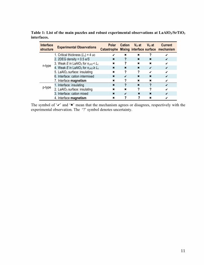
Table 1: List of the main puzzles and robust experimental observations at LaAlO3/SrTiO3 interfaces.
Interface structure Experimental Observations Polar
Catastrophe Cation Mixing
VO at interface
VO at surface
Current mechanism
n-type
1. Critical thickness (Lc) = 4 uc ✔ ✖ ✖ ? ✔ 2. 2DEG density < 0.5 e/S ✖ ? ✖ ✖ ✔ 3. Weak E in LaAlO3 for nLAO < Lc ✖ ? ✖ ✖ ✔ 4. Weak E in LaAlO3 for nLAO ≥ Lc ✖ ✖ ✖ ✔ ✔ 5. LaAlO3 surface: insulating ✖ ? ? ✔ ✔ 6. Interface: cation intermixed ✖ ✔ ✖ ✖ ✔ 7. Interface magnetism ✖ ? ✖ ✖ ✔
p-type
1. Interface: insulating ✖ ? ✖ ? ✔ 2. LaAlO3 surface: insulating ✖ ✖ ? ? ✔ 3. Interface: cation mixed ✖ ✔ ✖ ✖ ✔
4. Interface magnetism ✖ ? ? ✖ ✔
The symbol of ‘✔’ and ‘✖’ mean that the mechanism agrees or disagrees, respectively with the experimental observation. The ‘?’ symbol denotes uncertainty.
12
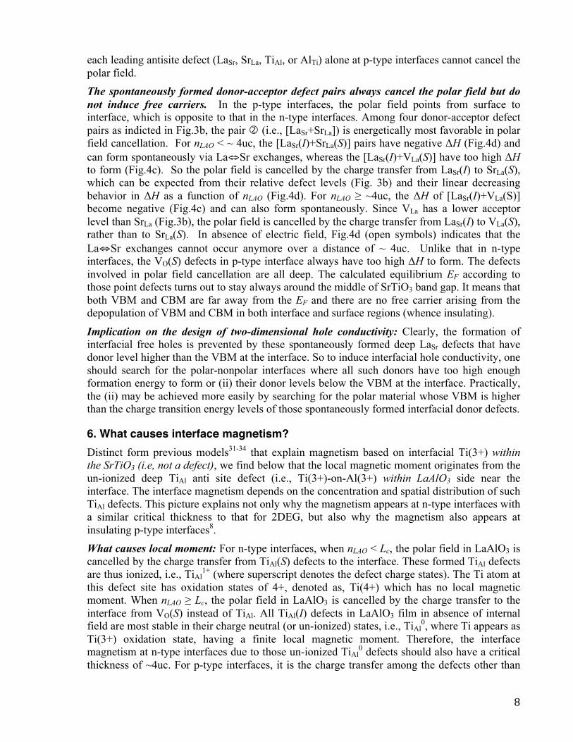
Figure 1: Schematic band and defect level picture for the unifying mechanism. a, n-type interfaces with nLAO < Lc: The electrons transfer from TiAl(S) to AlTi(I) and compensate the electric field in LaAlO3, inducing no itinerant carriers to the interface. b, n-type interfaces with nLAO ≥ Lc: The electrons transfer from VO(S) to interface. Part of interface charge is trapped by the deep AlTI acceptor defects. The deep TiAl
0 donor defects are confined within LaAlO3 near the interface and are not ionized, i.e., Ti3+-on-Al3+, having local magnetic moments. c, p-type interfaces with nLAO < Lc (~4uc): The electrons transfer from LaSr(I) to SrLa(S) and compensates the electric field in LaAlO3. d, p-type interfaces with nLAO ≥ Lc: The electrons transfer from LaSr(I) to VLa(S) and compensate the field in LaAlO3. The superscripts (0,+,++,-) denote the defect charge states, not the oxidation states of the ions there.
13
Figure 2: Formation energy of the interfacial point defects at thermodynamical equilibrium Fermi energy. a,b, n-type interfaces with nLAO < Lc and nLAO ≥ Lc, respectively. c, p-type interfaces. At a given EF, the defect in different charge states (e.g., VSr
0, VSr1-, VSr
2-) usually has different ΔH and the only one with the lowest ΔH is shown in the Figure. Other cation defects that have higher ΔH are shown in Supplementary Fig. 3. The chemical potentials used for Sr, Ti, La, Al, and O are -4.36, -6.20, -6.10, -5.46, and -2.0 eV respectively, relative to their corresponding elemental solid or gas phases, which corresponds to T=1050 K and PO2 = 6.1×10⁻⁶ Torr.

14
Figure 3: Defect charge transition energy levels of the interfacial point. a, n-type interface. b, p-type interface. The defect charge transition energy level is defined as the EF where the ΔH of a given defect in two different charge states equal. Some defects may have multiple charge transition energy levels. For example, VSr has the two transition energy levels (one is for the transition between neutral charge state and -1, and the other is between -1 and -2). In such case, if the defect is donor (red), only the lowest level is shown, and if the defect is acceptor (blue), the highest level is shown.

15
Figure 4: Properties of surface defects and defect complexes. a, the GGA-calculated ΔH of VO(s) defect, under the O-rich growth condition (i.e., ΔμO = -1.5 eV, Supplementary Fig. 2a). b, the ΔH of [TiAl+AlTi] defect pair created from a Ti⇔Al exchange out of the ideal interface with and without a VO(S) in a 2x2 6STO/4LAO/vacuum surpercell. c, the GGA-calculated ΔH of [LaSr(I)+VLa(S)] defect complex as a function of nLAO, under ΔμSr = -4.36 eV (Supplementary Fig. 1b). d, the ΔH of [LaSr+SrLa] defect pair created from a La⇔Sr exchange out of the ideal interface with and without a VLa(S) in a 2x2 6STO/4LAO/vacuum surpercell, respectively. The dTi⇔Al and dLa⇔Sr in b,d are the distance between the components of corresponding defect pair. The orange lines are the guides to the eye.

16
References 1 Hwang, H. Y. et al. Emergent phenomena at oxide interfaces. Nat Mater 11, 103-‐113
(2012). 2 Mannhart, J. & Schlom, D. G. Oxide Interfaces-‐An Opportunity for Electronics.
Science 327, 1607-‐1611 (2010). 3 Ohtomo, A. & Hwang, H. Y. A high-‐mobility electron gas at the LaAlO3/SrTiO3
heterointerface. Nature 427, 423-‐426 (2004). 4 Thiel, S., Hammerl, G., Schmehl, A., Schneider, C. W. & Mannhart, J. Tunable quasi-‐
two-‐dimensional electron gases in oxide heterostructures. Science 313, 1942-‐1945 (2006).
5 Brinkman, A. et al. Magnetic effects at the interface between non-‐magnetic oxides. Nat Mater 6, 493-‐496 (2007).
6 Li, L., Richter, C., Mannhart, J. & Ashoori, R. C. Coexistence of magnetic order and two-‐dimensional superconductivity at LaAlO3/SrTiO3 interfaces. Nat Phys 7, 762-‐766 (2011).
7 Ariando et al. Electronic phase separation at the LaAlO3/SrTiO3 interface. Nat Commun 2, 188 (2011).
8 Kalisky, B. et al. Critical thickness for ferromagnetism in LaAlO3/SrTiO3 heterostructures. Nat Commun 3, 922 (2012).
9 Salman, Z. et al. Nature of Weak Magnetism in SrTiO3/LaAlO3 Multilayers. Phys Rev Lett 109, 257207 (2012).
10 Lee, J. S. et al. Titanium d(xy) ferromagnetism at the LaAlO3/SrTiO3 interface. Nat Mater 12, 703-‐706 (2013).
11 Joshua, A., Ruhman, J., Pecker, S., Altman, E. & Ilani, S. Gate-‐tunable polarized phase of two-‐dimensional electrons at the LaAlO3/SrTiO3 interface. P Natl Acad Sci USA 110, 9633-‐9638 (2013).
12 Chen, H. H., Kolpak, A. M. & Ismail-‐Beigi, S. Electronic and Magnetic Properties of SrTiO3/LaAlO3 Interfaces from First Principles. Adv Mater 22, 2881-‐2899 (2010).
13 Chakhalian, J., Millis, A. J. & Rondinelli, J. Whither the oxide interface. Nat Mater 11, 92-‐94 (2012).
14 Siemons, W. et al. Origin of charge density at LaAlO3 on SrTiO3 heterointerfaces: Possibility of intrinsic doping. Phys Rev Lett 98, 196802 (2007).
15 Kalabukhov, A. et al. Effect of oxygen vacancies in the SrTiO3 substrate on the electrical properties of the LaAlO3/SrTiO3 interface. Phys Rev B 75, 121404 (2007).
16 Herranz, G. et al. High mobility in LaAlO3/SrTiO3 heterostructures: Origin, dimensionality, and perspectives. Phys Rev Lett 98, 216803 (2007).
17 Cen, C. et al. Nanoscale control of an interfacial metal-‐insulator transition at room temperature. Nat Mater 7, 298-‐302, doi:Doi 10.1038/Nmat2136 (2008).
18 Zhong, Z. C., Xu, P. X. & Kelly, P. J. Polarity-‐induced oxygen vacancies at LaAlO3/SrTiO3 interfaces. Phys Rev B 82, 165127 (2010).
19 Bristowe, N. C., Littlewood, P. B. & Artacho, E. Surface defects and conduction in polar oxide heterostructures. Phys Rev B 83, 205405 (2011).
20 Li, Y., Phattalung, S. N., Limpijumnong, S., Kim, J. & Yu, J. Formation of oxygen vacancies and charge carriers induced in the n-‐type interface of a LaAlO3 overlayer on SrTiO3(001). Phys Rev B 84, 245307 (2011).

17
21 Takizawa, M., Tsuda, S., Susaki, T., Hwang, H. Y. & Fujimori, A. Electronic charges and electric potential at LaAlO3/SrTiO3 interfaces studied by core-‐level photoemission spectroscopy. Phys Rev B 84, 245124 (2011).
22 Berner, G. et al. Direct k-‐Space Mapping of the Electronic Structure in an Oxide-‐Oxide Interface. Phys Rev Lett 110, 247601 (2013).
23 Nakagawa, N., Hwang, H. Y. & Muller, D. A. Why some interfaces cannot be sharp. Nat Mater 5, 204-‐209, doi:Doi 10.1038/Nmat1569 (2006).
24 Willmott, P. R. et al. Structural basis for the conducting interface between LaAlO3 and SrTiO3. Phys Rev Lett 99, 155502 (2007).
25 Kalabukhov, A. S. et al. Cationic Disorder and Phase Segregation in LaAlO3/SrTiO3 Heterointerfaces Evidenced by Medium-‐Energy Ion Spectroscopy. Phys Rev Lett 103, 146101 (2009).
26 Yamamoto, R. et al. Structural Comparison of n-‐Type and p-‐Type LaAlO3/SrTiO3 Interfaces. Phys Rev Lett 107, 036104 (2011).
27 Qiao, L., Droubay, T. C., Kaspar, T. C., Sushko, P. V. & Chambers, S. A. Cation mixing, band offsets and electric fields at LaAlO3/SrTiO3(001) heterojunctions with variable La:Al atom ratio. Surf Sci 605, 1381-‐1387 (2011).
28 Vonk, V. et al. Polar-‐discontinuity-‐retaining A-‐site intermixing and vacancies at SrTiO3/LaAlO3 interfaces. Phys Rev B 85, 045401 (2012).
29 Gunkel, F. et al. Influence of charge compensation mechanisms on the sheet electron density at conducting LaAlO3/SrTiO3-‐interfaces. Appl Phys Lett 100, 052103 (2012).
30 Salluzzo, M. et al. Origin of Interface Magnetism in BiMnO3/SrTiO3 and LaAlO3/SrTiO3 Heterostructures. Phys Rev Lett 111, 087204 (2013).
31 Banerjee, S., Erten, O. & Randeria, M. Ferromagnetic exchange, spin-‐orbit coupling and spiral magnetism at the LaAlO3/SrTiO3 interface. Nat Phys 9, 625-‐629 (2013).
32 Fidkowski, L., Jiang, H. C., Lutchyn, R. M. & Nayak, C. Magnetic and superconducting ordering in one-‐dimensional nanostructures at the LaAlO3/SrTiO3 interface. Phys Rev B 87, 014436 (2013).
33 Michaeli, K., Potter, A. C. & Lee, P. A. Superconducting and Ferromagnetic Phases in SrTiO3/LaAlO3 Oxide Interface Structures: Possibility of Finite Momentum Pairing. Phys Rev Lett 108, 117003 (2012).
34 Pavlenko, N., Kopp, T., Tsymbal, E. Y., Mannhart, J. & Sawatzky, G. A. Oxygen vacancies at titanate interfaces: Two-‐dimensional magnetism and orbital reconstruction. Phys Rev B 86, 064431 (2012).
35 Higuchi, T. & Hwang, H. Y. in Multifunctional oxide heterostructures (eds E. Y. Tsymbal, E. R. A. Dagotto, Chang-‐Beom Eom, & R. Ramesh) (Oxford University Press, 2012).
36 Janotti, A., Bjaalie, L., Gordon, L. & Van de Walle, C. G. Controlling the density of the two-‐dimensional electron gas at the SrTiO3/LaAlO3 interface. Phys Rev B 86, 241108 (2012).
37 Segal, Y., Ngai, J. H., Reiner, J. W., Walker, F. J. & Ahn, C. H. X-‐ray photoemission studies of the metal-‐insulator transition in LaAlO3/SrTiO3 structures grown by molecular beam epitaxy. Phys Rev B 80, 241107 (2009).
38 Huang, B. C. et al. Mapping Band Alignment across Complex Oxide Heterointerfaces. Phys Rev Lett 109, 246807 (2012).
18
39 Slooten, E. et al. Hard x-‐ray photoemission and density functional theory study of the internal electric field in SrTiO3/LaAlO3 oxide heterostructures. Phys Rev B 87, 085128 (2013).
40 Berner, G. et al. Band alignment in LaAlO3/SrTiO3 oxide heterostructures inferred from hard x-‐ray photoelectron spectroscopy. Phys Rev B 88, 115111 (2013).
41 Van de Walle, C. G. & Neugebauer, J. First-‐principles calculations for defects and impurities: Applications to III-‐nitrides. J Appl Phys 95, 3851-‐3879 (2004).
42 Warusawithana, M. P. R., C.; Mundy, J. A.;Roy, P.; Ludwig, J.; Paetel, S.; Heeg, T.; Pawlicki, A. A.; Kourkoutis, L. F.; Zheng, M.; Lee, M.; Mulcahy, B.; Zander, W.; Zhu, Y.; Schubert, J.; Eckstein, J. N.; Muller, D. A.; Hellberg, C. S.; Mannhart, J.; Schlom, D. G. LaAlO3 stoichiometry is key to electron liquid formation at LaAlO3/SrTiO3 interfaces. Nat Commun 4, 2351 (2013).
43 Zhang, L. X. et al. Origin of insulating behavior of the p-‐type LaAlO3/SrTiO3 interface: Polarization-‐induced asymmetric distribution of oxygen vacancies. Phys Rev B 82,125412 (2010).
44 Xie, Y. W., Hikita, Y., Bell, C. & Hwang, H. Y. Control of electronic conduction at an oxide heterointerface using surface polar adsorbates. Nat Commun 2, 494 (2011).
45 Bi, F. et al. "Water-‐cycle" mechanism for writing and erasing nanostructures at the LaAlO3/SrTiO3 interface. Appl Phys Lett 97, 173110 (2010).
46 Son, W. J., Cho, E., Lee, J. & Han, S. Hydrogen adsorption and carrier generation in LaAlO3-‐SrTiO3 heterointerfaces: a first-‐principles study. J Phys-‐Condens Mat 22, 315501 (2010).
47 Arras, R., Ruiz, V. G., Pickett, W. E. & Pentcheva, R. Tuning the two-‐dimensional electron gas at the LaAlO3/SrTiO3(001) interface by metallic contacts. Phys Rev B 85, 125404 (2012).
48 Liu, Z. Q. et al. Origin of the Two-‐Dimensional Electron Gas at LaAlO3/SrTiO3 Interfaces: The Role of Oxygen Vacancies and Electronic Reconstruction. Phys Rev X 3, 021010 (2013).
49 Reinle-‐Schmitt, M. L. et al. Tunable conductivity threshold at polar oxide interfaces. Nat Commun 3, 932 (2012).
50 Dingle, R., Stormer, H. L., Gossard, A. C. & Wiegmann, W. Electron Mobilities in Modulation-‐Doped Semiconductor Heterojunction Super-‐Lattices. Appl Phys Lett 33, 665-‐667 (1978).
51 Chambers, S. A. et al. Instability, intermixing and electronic structure at the epitaxial LaAlO3/SrTiO3(001) heterojunction. Surf Sci Rep 65, 317-‐352 (2010).
52 Popovic, Z. S., Satpathy, S. & Martin, R. M. Origin of the Two-‐Dimensional Electron Gas Carrier Density at the LaAlO3 on SrTiO3 Interface. Phys Rev Lett 101, 256801 (2008).
53 Son, W. J., Cho, E., Lee, B., Lee, J. & Han, S. Density and spatial distribution of charge carriers in the intrinsic n-‐type LaAlO3-‐SrTiO3 interface. Phys Rev B 79, 245411 (2009).
54 Seo, S. S. A. et al. Multiple conducting carriers generated in LaAlO3/SrTiO3 heterostructures. Appl Phys Lett 95, 082107 (2009).
55 Delugas, P. et al. Spontaneous 2-‐Dimensional Carrier Confinement at the n-‐Type SrTiO3/LaAlO3 Interface. Phys Rev Lett 106, 166807 (2011).
56 Moetakef, P. et al. Electrostatic carrier doping of GdTiO3/SrTiO3 interfaces. Appl Phys Lett 99, 232116 (2011).
19
57 Pentcheva, R. & Pickett, W. E. Charge localization or itineracy at LaAlO3/SrTiO3 interfaces: Hole polarons, oxygen vacancies, and mobile electrons. Phys Rev B 74, 035112 (2006).
58 Sing, M. et al. Profiling the Interface Electron Gas of LaAlO3/SrTiO3 Heterostructures with Hard X-‐Ray Photoelectron Spectroscopy. Phys Rev Lett 102, 176805 (2009).
59 Park, J. et al. Oxygen-‐Vacancy-‐Induced Orbital Reconstruction of Ti Ions at the Interface of LaAlO3/SrTiO3 Heterostructures: A Resonant Soft-‐X-‐Ray Scattering Study. Phys Rev Lett 110, 017401 (2013).
60 Blochl, P. E. Projector Augmented-‐Wave Method. Phys Rev B 50, 17953-‐17979 (1994).
61 Kresse, G. & Furthmuller, J. Efficiency of ab-‐initio total energy calculations for metals and semiconductors using a plane-‐wave basis set. Comp Mater Sci 6, 15-‐50 (1996).
62 Perdew, J. P., Burke, K. & Ernzerhof, M. Generalized gradient approximation made simple. Phys Rev Lett 77, 3865-‐3868 (1996).
63 Yu, L. P., Ranjan, V., Lu, W., Bernholc, J. & Nardelli, M. B. Equivalence of dipole correction and Coulomb cutoff techniques in supercell calculations. Phys Rev B 77, 245102 (2008).
64 Heyd, J., Scuseria, G. E. & Ernzerhof, M. Hybrid functionals based on a screened Coulomb potential (vol 118, pg 8207, 2003). J Chem Phys 124, 219906 (2006).
65 Persson, C., Zhao, Y. J., Lany, S. & Zunger, A. n-‐type doping of CuInSe2 and CuGaSe2. Phys Rev B 72, 035211 (2005).
66 Freysoldt, C. et al. First-‐principles calculations for point defects in solids. Rev. Mod. Phys. 86 (2014).

20
Supplementary Information for “A polarity-induced defect mechanism for conductivity and magnetism at oxide interfaces” by Liping Yu and Alex Zunger
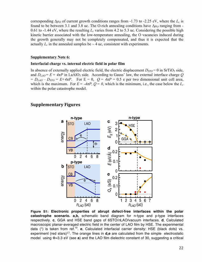
Supplementary Note 1: The failures of polar catastrophe model The key argument in favor of the polar catastrophe mechanism is its predicted critical thickness (Lc) of metal-insulator transition. Both electrostatics and the first principles calculations based on density functional theory (DFT) with the generalized gradient approximation (GGA)1, shown in Fig. S1c lead to an Lc between three and four unit cells2,3. However, these results may be clouded by specific uncertainties: the electrostatic model depends on the choice of the LAO film dielectric constant and LAO/STO band offsets, whereas the GGA calculation suffers from the well-known band gap underestimation problem4. To examine this point we have applied the HSE hybrid functional5, which predicts correctly the experimental bulk STO band gap of 3.2 eV. We find an Lc of 4-5 uc (Fig. S2c). It is noteworthy that, for nLAO = 4 uc, the band gap of the system turns out to be 1.1 eV, suggesting an insulating behavior, contrasting with the experiment where the robust conductivity has been observed at this thickness. Hence, strictly speaking, the defect-free polar catastrophe model cannot explain the Lc either6.
In a defect-free interface structure, both previous DFT-GGA calculations7,8 and our HSE calculation (Fig.S2d) predict a large electric field of 0.19 V/Å in the LAO film of nLAO < Lc, which decreases gradually as nLAO increases for nLAO ≥ Lc, approaching zero only at infinitely thick nLAO. This prediction of the PC model conflicts with experiments, where only very weak residual field has been observed for all investigated nLAO
9-12.
Supplementary Note 2: Thermodynamical equilibrium Fermi energy as a function of LaAlO3 thickness Under a given growth condition, the thermodynamic equilibrium EF is established as a balance of all electrons and holes concentrations contributed by thermal ionization of all considered defects. According to charge neutrality condition13, the EF can be calculated self-consistently from first principles using defect formation energies as inputs.
As seen in the main text, the charge transfer from surface defect to interface defect always cancels the built-in polar field. For the n-type interface below the critical thickness and p-type interfaces at any thickness, all involved defects are deep defects, the resulting equilibrium EF always sits near the middle of SrTiO3 band gap. While for n-type interfaces above the critical thickness, the surface O vacancies (VO) form spontaneously. This VO defect has a donor level higher than the SrTiO3 conduction band at the interface. The electrons will be transferred from Vo donor level to the SrTiO3 conduction bands and pins the EF near the SrTiO3 valence band minimum. Supplementary Note 3: Justification for the thermodynamic equilibrium The thin film growth is an out of equilibrium process. Our thermodynamic calculations may be still applied. The more detailed justification can be found in Ref [14]. In brief, the calculated
21
formation energies and defect levels (deep or shallow) in this work are physically meaningful for both equilibrium and non-equilibrium processes. Non-equilibrium implies that once certain high-energy defects form, kinetic barriers may preserve them, even if their concentration exceeds the nominal equilibrium value. However, it should be clear that defects with high formation energy would always be unlikely to form, since a lot of energy needs to be expended in their creation, and the driving force to lowering the energy is large.
Supplementary Note 4: The formation !! of VO(S) vs LAO film thickness nLAO The linear decreasing of ΔH of VO(S) with increasing nLAO can be understood easily from the opposite dipole created by the charge transfer from VO(S) to the interface.
In a supercell calculation, the formation energy of an oxygen vacancy at LAO surface (denoted as VO (s) hereafter) is
Δ! = ℰ!! + !!LAO!! − ℰ!! + !"LAO! + !!, (1)
where ℰ!! and ℰ!! are the total energies of the supercell structures in the absence of an electric field across the LAO film with and without the vacancy. The second term in each of the brackets corresponds to the electrostatic energy rise due to the presence of internal electric field !! and E in LAO with and without VO, respectively. In a 2×2 2D supercell considered here the creation of a single VO (S) leads to zero electric field in LAO (!!= 0 for all nLAO).8,15,16
Thus, Eq. (1) reduces to Δ! = ℰ!!−ℰ!! + !! − !!LAO!, where the second term can now be viewed as an opposite dipole, which decreases linearly at a rate of eE as nLAO increases. Therefore, the larger the nLAO, the larger the opposite dipole moment that lowers the total energy of the system, and the more energy decrease in ΔH. For VO(I) defects, which can not create an opposite dipole that lowers the ΔH, the ΔH is thus independent of nLAO and remains high as nLAO increases8. The slope dΔH/dnLAO) remains same or almost same as VO(S) defects accumulate gradually. This is because that the built-in polar field is created by the polar charge at surface/interface. Microscopically, the electron transfer from “one VO(S)” to the “interface” mainly cancels the polar field caused by the “polar charge at this VO(S) site”, not the “polar field caused by the polar charge at other VO(S) defect sites”. It means that during gradual formation of VO(S), though the in-plane-averaged electric field is lowered, each VO(S) to be formed still face the (almost) same polar field to be cancelled by it. Hence, the decrease in ΔH of VO(S) should be almost same as VO(S) defects accumulates. This thus explains why the metal-insulator transition due to VO(S) is sharp. Supplementary Note 5: Critical thickness vs oxygen chemical potential
Eq.(1) suggests that the critical Lc can be approximately determined by the ΔH of the interfacial VO in TiO2 layer and the electric field E in the defect-free LAO film (from electrostatics), via
!! = [ℰ!!−ℰ!! + !!]/!", (2) which is a function of the oxygen chemical potential µO and the built-in electric field in defect-free LAO. Supplementary Figure 1b shows the variation of resulting Lc due to VO (S) with respect to ΔµO (i.e., the oxygen chemical potential relative to 1/2O2) at T = 0K. The
22
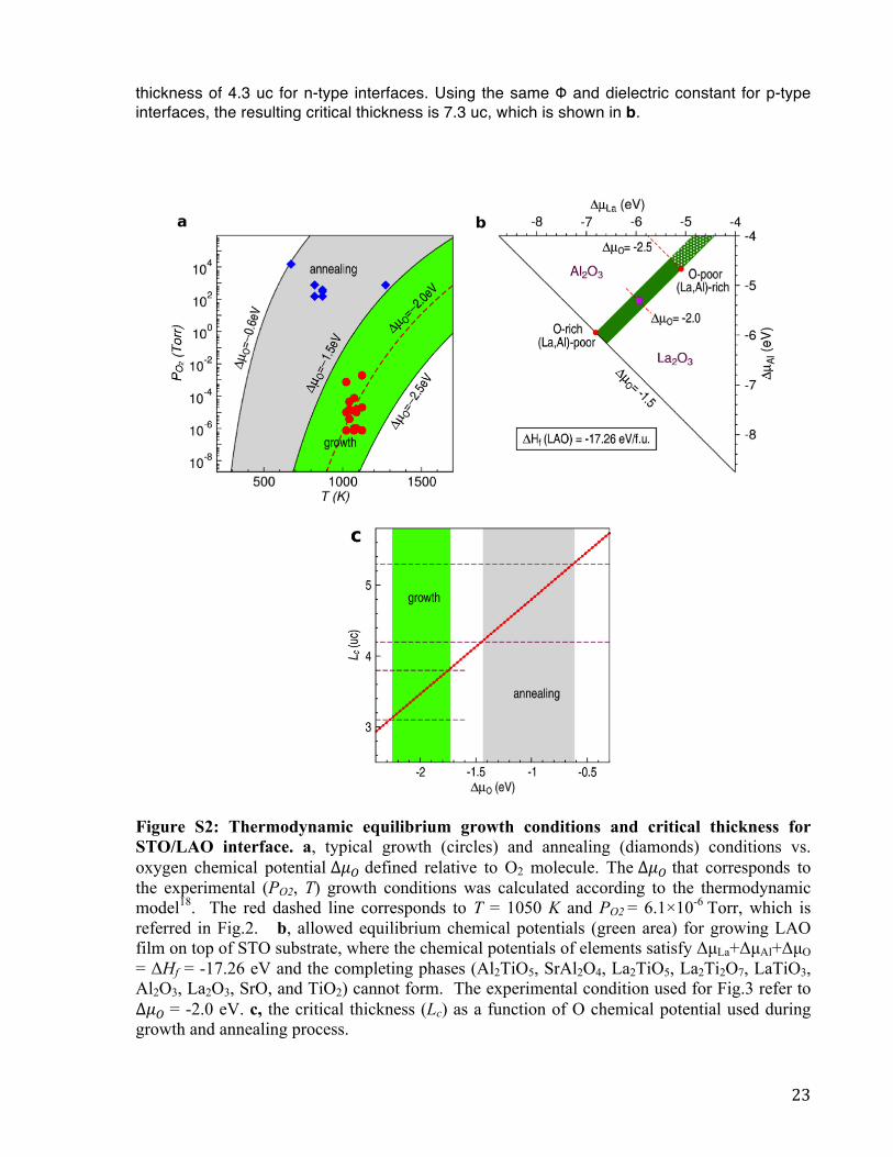
corresponding ΔµO of current growth conditions ranges from -1.73 to -2.25 eV, where the Lc is found to be between 3.1 and 3.8 uc. The O-rich annealing conditions have ΔµO ranging from -0.61 to -1.44 eV, where the resulting Lc varies from 4.2 to 5.3 uc. Considering the possible high kinetic barrier associated with the low-temperature annealing, the O vacancies induced during the growth generally may not be completely compensated, and thus it is expected that the actually Lc in the annealed samples be ~ 4 uc, consistent with experiments.
Supplementary Note 6: Interfacial charge vs. internal electric field in polar film In absence of externally applied electric field, the electric displacement DSTO = 0 in SrTiO3 side, and DLAO = E + 4πP in LaAlO3 side. According to Gauss’ law, the external interface charge Q = DLAO – DSTO = E+4πP. For E = 0, Q = 4πP = 0.5 e per two dimensional unit cell area, which is the maximum. For E = -4πP, Q = 0, which is the minimum, i.e., the case below the Lc within the polar catastrophe model.
Supplementary Figures
Figure S1: Electronic properties of abrupt defect-free interfaces within the polar catastrophe scenario. a,b, schematic band diagram for n-type and p-type interfaces respectively. c, GGA and HSE band gaps of 6STO/nLAO/vacuum interfaces. d, Calculated macroscopic planar-averaged electric field in the center of LAO film by HSE. The experimental data (*) is taken from ref.10. e, Calculated interfacial carrier density: HSE (black dots) vs. experiment (red stars)17. The orange lines in d,e are calculated from the simple electrostatic model using Φ=3.3 eV (see a) and the LAO film dielectric constant of 30, suggesting a critical
23
thickness of 4.3 uc for n-type interfaces. Using the same Φ and dielectric constant for p-type interfaces, the resulting critical thickness is 7.3 uc, which is shown in b.
Figure S2: Thermodynamic equilibrium growth conditions and critical thickness for STO/LAO interface. a, typical growth (circles) and annealing (diamonds) conditions vs. oxygen chemical potential ∆!! defined relative to O2 molecule. The ∆!! that corresponds to the experimental (PO2, T) growth conditions was calculated according to the thermodynamic model18. The red dashed line corresponds to T = 1050 K and PO2 = 6.1×10⁻⁶ Torr, which is referred in Fig.2. b, allowed equilibrium chemical potentials (green area) for growing LAO film on top of STO substrate, where the chemical potentials of elements satisfy ΔµLa+ΔµAl+ΔµO = ΔHf = -17.26 eV and the completing phases (Al2TiO5, SrAl2O4, La2TiO5, La2Ti2O7, LaTiO3, Al2O3, La2O3, SrO, and TiO2) cannot form. The experimental condition used for Fig.3 refer to ∆!! = -2.0 eV. c, the critical thickness (Lc) as a function of O chemical potential used during growth and annealing process.

24
Figure S3: Properties of interfacial defects in the 6STO/2LAO heterostructure containing both n-‐type and p-‐type interfaces. a, n-type interface. b, p-type interface. Each panel in a,b shows various defects in a given atomic layer. Each line represents the ΔH of a donor (red) or acceptor (blue) defect. Different slops of line segments represent different charge states of a defect that are most stable at given EF. Open circles mark the defect charge transition energies, i.e., the EF where the formation energy of a defect in two different charge states equal. The shaded regions in each panel denote the variation range of the equilibrium EF. The chemical potentials for Sr, Ti, La, Al, and O are -4.36, -6.20, -6.10, -5.46, and -2.0 eV respectively, relative to their corresponding elemental solid or gas phases, which corresponds to T=1050 K and PO2 = 6.1×10⁻⁶ Torr.
References 1 Perdew, J. P., Burke, K. & Ernzerhof, M. Generalized gradient approximation made
simiple simple. Phys Rev Lett 77, 3865-‐3868 (1996). 2 Lee, J. & Demkov, A. A. Charge origin and localization at the n-‐type SrTiO3/LaAlO3
interface. Phys Rev B 78, 193104 (2008). 3 Reinle-‐Schmitt, M. L. et al. Tunable conductivity threshold at polar oxide interfaces.
Nat Commun 3, 932 (2012). 4 Perdew, J. P. & Levy, M. Physical Content of the Exact Kohn-‐Sham Orbital Energies -‐
Band-‐Gaps and Derivative Discontinuities. Phys Rev Lett 51, 1884-‐1887 (1983). 5 Heyd, J., Scuseria, G. E. & Ernzerhof, M. Hybrid functionals based on a screened
Coulomb potential (vol 118, pg 8207, 2003). J Chem Phys 124, 219906 (2006).
25
6 Cossu, F., Schwingenschlogl, U. & Eyert, V. Metal-‐insulator transition at the LaAlO3/SrTiO3 interface revisited: A hybrid functional study. Phys Rev B 88, 045119 (2013).
7 Pentcheva, R. & Pickett, W. E. Avoiding the Polarization Catastrophe in LaAlO3 Overlayers on SrTiO3(001) through Polar Distortion. Phys Rev Lett 102, 107602 (2009).
8 Li, Y., Phattalung, S. N., Limpijumnong, S., Kim, J. & Yu, J. Formation of oxygen vacancies and charge carriers induced in the n-‐type interface of a LaAlO3 overlayer on SrTiO3(001). Phys Rev B 84, 245307 (2011).
9 Segal, Y., Ngai, J. H., Reiner, J. W., Walker, F. J. & Ahn, C. H. X-‐ray photoemission studies of the metal-‐insulator transition in LaAlO3/SrTiO3 structures grown by molecular beam epitaxy. Phys Rev B 80, 241107 (2009).
10 Huang, B. C. et al. Mapping Band Alignment across Complex Oxide Heterointerfaces. Phys Rev Lett 109, 246807 (2012).
11 Slooten, E. et al. Hard x-‐ray photoemission and density functional theory study of the internal electric field in SrTiO3/LaAlO3 oxide heterostructures. Phys Rev B 87, 085128 (2013).
12 Berner, G. et al. Band alignment in LaAlO3/SrTiO3 oxide heterostructures inferred from hard x-‐ray photoelectron spectroscopy. Phys Rev B 88, 115111 (2013).
13 Persson, C., Zhao, Y. J., Lany, S. & Zunger, A. n-‐type doping of CuInSe2 and CuGaSe2. Phys Rev B 72, 035211 (2005).
14 Van de Walle, C. G. & Neugebauer, J. First-‐principles calculations for defects and impurities: Applications to III-‐nitrides. J Appl Phys 95, 3851-‐3879 (2004).
15 Cen, C. et al. Nanoscale control of an interfacial metal-‐insulator transition at room temperature. Nat Mater 7, 298-‐302 (2008).
16 Pavlenko, N., Kopp, T., Tsymbal, E. Y., Mannhart, J. & Sawatzky, G. A. Oxygen vacancies at titanate interfaces: Two-‐dimensional magnetism and orbital reconstruction. Phys Rev B 86, 064431 (2012).
17 Thiel, S., Hammerl, G., Schmehl, A., Schneider, C. W. & Mannhart, J. Tunable quasi-‐two-‐dimensional electron gases in oxide heterostructures. Science 313, 1942-‐1945 (2006).
18 Osorio-‐Guillen, J., Lany, S., Barabash, S. V. & Zunger, A. Magnetism without magnetic ions: Percolation, exchange, and formation energies of magnetism-‐promoting intrinsic defects in CaO. Phys Rev Lett 96, 107203 (2006).