a practical guide to low-power design freescale: … design, vt optimization, memory bitcell design,...
TRANSCRIPT

A Practical Guide to Low-Power DesignUser Experience with CPF
Freescale: Wireless Low-Power Design and Verification with CPF
Sec6:2
Freescale: Wireless Low-Power Design and Verification with CPF
By Milind Padhye, Low-Power Design Manager, and David Gross, Low-Power/ Wireless Tools and Methodology Manager, Freescale Semiconductor, Wireless. © Freescale Semiconductor.Freescale is making the world a smarter place with leading embedded semiconductor solutions for cars, mobile phones, networks, and more. Freescale Semiconductor is a global leader in the design and manufacture of embedded semiconductors for the automotive, consumer, industrial, networking, and wireless markets. The privately held company is based in Austin, Texas, and has design, research and development, manufacturing, or sales operations in more than 30 countries. Freescale is one of the world’s largest semiconductor companies with 2007 sales of $5.8 billion. For mobile phones, Freescale delivers a full range of UMTS/WCDMA, EDGE, and GSM/GPRS platforms and components with a proven MXC Technology, the industry’s first single-core modem architecture.Freescale is a leader in portable media players and mobile entertainment devices, with incredibly efficient processors, miniaturized components, and the flexibility to handle multiple protocols, standards, and air interfaces: i.MX Applications Processors, Power Management and User Interface ICs, ColdFire® Audio Processors, and Mobile TV.Freescale was one of the founding members of the Power Forward Initiative and Si2 Low Power Coalition. Freescale has supported continuous development of the CPF language for the low-power design. As PFI advisors, we worked with all members to ensure that low-power design needs are properly addressed.Here we address the importance of power in cell phone design, a variety of techniques used to minimize the power consumption, challenges in wireless SoC for power-oriented design, and how a CPF-enabled flow deals with these challenges, along with power reduction results for a baseband processor design in 65nm.
Business Implications of PowerWireless and Handheld Devices
Standby time, talk time, and multimedia runtime in cell phones are the key performance parameters. They define the quality of the cell phone in consumers’ minds, and are highly publicized as competitive specifications.
Standby and talk time are benchmark parameters in the cell phone industry• Music playback time is a benchmark for MP3 capable phones• Frequent battery charging is a major negative in consumers’ minds• Increasing these times with a large battery means increased cost and weight• Increased heat in phone means lower reliability, increased liability, and higher • total cost of ownership
Sec6:2

Freescale: Wireless Low-Power Design and Verification with CPF
Sec6:3
The power/performance ratio must be very good to win in the market since consumers are becoming power-aware and make operational decisions with power specifications.
Wireless Carriers and Power
In the wireless market, the source of revenue is off for the carriers if the cell phone is turned off. Low-power design has a direct impact to carrier revenue and is a business critical need. Those electromagnetic waves are turned into dollar-magnetic only if the cell phone is alive! As cell phones are battery-operated devices, this puts a large emphasis on energy efficiency in all modes of phone operation. Performance is needed to sell the phone, and energy efficiency is needed to bring revenue for the carrier.
Phone Power and EnergyThe cell phone battery life is a function of both the static power consumed by the chips when in sleep mode, and active power consumed during the specific mode of activity when the phone is on.
Figure 131. Tower of power
Freescale: Wireless Low-Power Design and Verification with CPF
Sec6:4
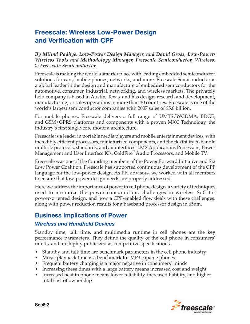
The standby power is determined by the leakage in the chip; the device leakage problem has increased significantly with advanced process nodes and the reduction of feature sizes. The standby mode of the phone is a continuous cycle of sleep and wakeup. The phone wakes up every cycle, connects to the base station to check the presence of a new call. In the absence of a call, the phone re-enters the sleep mode. This sequence and its frequency are specified by the particular wireless protocol supported by the phone. Thus, the protocol also determines the power consumption in the wireless SoC. This continuous cycle requires advanced low-power design to minimize the associated power consumption determined by the leakage of the chips in the platforms, and power consumed during the wakeup sequence. Since there is entry and exit cost associated with each wakeup and sleep cycle, a higher rate of wakeup and sleep cycles may lead to reduced standby time unless a variety of low-power design techniques are used to meet the battery life requirements for the specific wireless protocol.During sleep, minimum activity exists inside phone and hence leakage is major factor for power: This has driven the design goal to minimize leakage in sleep modes.
Phone Standby Current
Figure 132. Standby current for cell phones over the last 7 years
7280
FLDB ELV360
FLD01270
680
1Q
00 2
Q00
3Q
00 4
Q00
1Q
012Q
01 3
Q01
4Q
01 1
Q02
2Q
02 3
Q02
4Q
02 1
Q03
2Q
03 3
Q03
4Q
03 1
Q04
2Q04
3Q04
4Q04
1Q05
2Q05
3Q05
4Q05
1Q06
2Q06
3Q06
4Q06
1Q07
2Q07
3Q07
4Q07
GS
M S
tand
bu C
urre
nt (
mA
)9
8
7
1
2
3
4
5
6
SGH-C225
SGH-E317C331
9500
K700i
V600 V400 SGH-X407
V100
P900 T630
T68i
RCKR EL
V60g
3395
SGH-E400
NGage QDSGH-E105
V66
SGH-E317V360
FL007270
V638
6120
6810
S710 Z608 N90RAZR
6230
6830
7260W808
6200
Freescale: Wireless Low-Power Design and Verification with CPF
Sec6:5
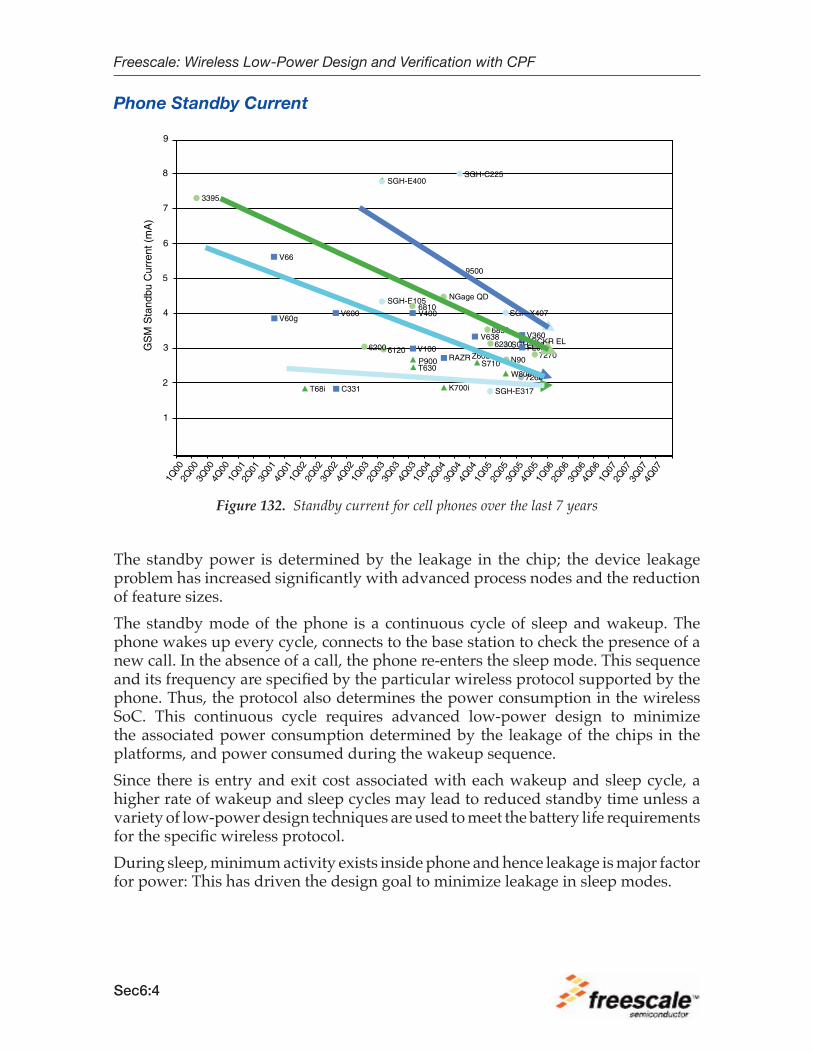
The modern cell phone is capable of a wide variety of targeted applications, including talk, multimedia, songs, internet, camera, voice activation, etc. Performance and components required for a voice call may be different when compared to other active modes such as multimedia playback operation. Each application has different performance needs, and application runtime is limited by battery life.The power/performance ratio must be optimized for target applications, and increased energy efficiency can be achieved by advanced design techniques like dynamic power reduction, such as clock gating and DVFS.
It’s About Energy
Granted, the goal is to extend phone battery life. Let’s examine both power and energy.
Figure 133. Talk current for cell phones over the last 7 years
9500
3395
6200 6010 62307270
880086208610
7260N90
NGage QD
6882
7500a
SGH-C225
SGH-X497
SGH-E100
SGH-E317
SGH-E730
SGH-E310V400V480
C331V600
RA7B V3V850B5DL
RCKR EL
V610
V60g
V66
K700iT600
T630
P600
VV0
T616
1Q
00 2
Q00
3Q
00 4
Q00
1Q
012Q
01 3
Q01
4Q
01 1
Q02
2Q
02 3
Q02
4Q
02 1
Q03
2Q
03 3
Q03
4Q
03 1
Q04
2Q04
3Q04
4Q04
1Q05
2Q05
3Q05
4Q05
1Q06
2Q06
3Q06
4Q06
1Q07
2Q07
3Q07
4Q07
250
0
50
100
150
200
350
300
GS
M V
oice
Cal
l Cur
rent
(m
A)
Phone Application Current

Freescale: Wireless Low-Power Design and Verification with CPF
Sec6:6
Total power is the sum of static and active power. Static power depends on DC currents (I), from current sources, reference circuits, PLLs and device leakage, as well as V (voltage). Active power is from digital switching, where α is the switching activity, C is capacitance, V is voltage, and F is frequency.
EnergyBattery life is proportional to energy consumed, where energy is power integrated over time.
Power
To extend battery life, wireless designers must manage energy consumption. In certain case, it may be beneficial to run a high-power application for a small duration as compared to running a low-power application for long durations. Low-power design should provide an infrastructure to support such energy management features.
Figure 134. Energy drain
Ptotal = ISTATIC V + αCV2F
ETOT = ∫ Ptotal dt

Freescale: Wireless Low-Power Design and Verification with CPF
Sec6:7
Power Problem
Attention to power throughout the entire design cycle greatly impacts battery life.Software definitions: Software can dynamically monitor the system and provide • advanced control of modules for energy savingsPlatform definitions: Defining optimal power modes and modules, with • associated power trees and connectivity, has a huge impactArchitectural definitions: Major power tradeoffs can be achieved at architectural • level of designDesign definitions in hardware design can specify the detailed implementation • of advanced power management techniques such as SRPG, clock gating, multiple supply voltages, power gating, dynamic voltage scaling, and biasing techniquesProcess node definitions must support low-power design with multi-• Vt libraries, memory and transistor design, and custom and analog blocks based on the physics of that process node
Figure 135. Low-power spans all levels
Dynamic system monitoring and intelligent control ofenergy saving
SoftwareDefinitions
Des
ign
Leve
lS
yste
m L
evel
PlatformDefinitions
ArchitecturalDefinitions
DesignDefinitions
Process NodeDefinitions
Power trees, connectivity of components, and consistent platform power modes
Heterogeneous processing resource optimization: MCU, DSP, accelerators, functional processing units
Hardware support for power gating, low-power idle modes,SRPG, AWB, DVFS, DPTC, biasing techniques
Transistor design, Vt optimization, memory bitcell design,special circuits, libraries, custom and analog blocks
Before CPF, conventional flows reached a bottleneck with advanced low-power techniques with significant impact on complexity, productivity, risk, and time to market. Design productivity is significantly impacted if the power-related issues are found at a late stage.Major issues seen with conventional non-CPF flows for low-power design:
No ability to express the low-power intent: Verilog has shown bottlenecks • and could not capture the power intent to establish a fully consistent flow for integration and verificationVerifying low-power features at RTL was a significant bottleneck•

Freescale: Wireless Low-Power Design and Verification with CPF
Sec6:8
Formal verification of low-power features has shown to be a major challenge, • requiring special tools and flowsVoltage variation has a significant impact on timing. Multi-voltage designs • created a large number of corners and analysis points. Timing convergence across multiple corners is equally challenging and can cause multiple iterationsDebugging a low-power design is complex. If part of the design is powered off • due to a bug, it cannot be debugged any further. Careful analysis and debug structures are essential for low-power silicon success
Static Power Design Challenge and Design Techniques
Since static power is crucial for defining the standby time of cell phones, Freescale Wireless has defined and implements multiple leakage reduction techniques:
State retention power gating (SRPG)• Save and restore with power gating (S&RPG)• Complete power shut-off with isolation (PSO)• Multi-• Vt design stylesAggressive voltage reduction during standby mode (RV)• Device biasing techniques•
Silicon design with combination of such techniques is very complex and consistent representation, implementation, and verification is crucial for silicon success.
State Retention Power Gating (SRPG)
SRPG is an advanced technique to minimize leakage in sleep modes, combining active performance and reduced leakage in idle mode.The state of the system is typically saved in flip-flops and memory elements. Combinatorial logic between the flip-flops propagates the state. In idle modes, the system clock is held low and the storage elements save the state. However, the combinatorial logic can dissipate significant leakage power. SRPG reduces leakage in all non-active portions of the design.
Figure 136. State Retention Power Gating
In_1
In_
clk
ff
ff
ff
Combinational
vdd
vddc

Freescale: Wireless Low-Power Design and Verification with CPF
Sec6:9
As shown above, Vddc is a continuous power supply while Vdd is an interruptible power supply. Both supplies can be driven from the same source, but Vdd is power switched with on/off gates. These control the Vdd grid based on recognition of the sleep mode of the chip. With this technique, a very small part of the design is connected to the always-on supply. Significant leakage can be saved, depending on the number of flops and their ratio to combinatorial logic.
Save and Restore Power Gating (S&RPG)
S&R PG is another popular technique used for leakage saving, similar to SRPG, but with different implementation. Before entering the low-power sleep mode, the state of the system is captured and converted to a memory array image instead of saving it locally inside the flop. After moving the state to memory, the appropriate module of the system is powered off. The memory array saving the state is kept alive through the duration of power off. At wakeup, the module is powered up with a reset condition and the previous state is downloaded from memory.Power is associated with moving the state back and forth from module to memory. For smaller duration sleep modes, it may not be an effective way to reduce the power consumption. This technique also impacts the wakeup latency since it takes much longer to save and restore from memory, compared to SRPG where each register is restored locally.
As shown above, S1,S2…Sn are modules that share the same power controller and memory array for saving during power down. The controller also turns off the power gates G1, G2.. Gn once the appropriate state transfer is complete. This design technique can increase overall complexity of power control significantly as compared to SRPG. The latency of wakeup and sleep is also dependent on data bus width, controller operating frequency, and overall throughput of the memory controller.
Figure 137. Save and Restore Power Gating
S1
S2
Sn
MemoryArrayand
Control
PowerController
VDD
G1
G2
Gn
Freescale: Wireless Low-Power Design and Verification with CPF
Sec6:10
Biasing and Multi-Vt
Biasing techniques and multi-Vt adjustments are popular to control the power and performance of the design. High-Vt libraries, when mixed with low-Vt devices in critical timing path, provide power/performance optimization. When leakage cannot be mitigated using mixed-Vt, power gating is better for leakage reduction.
Active Power Challenge and Design TechniquesActive power during the wakeup and connection to base station is also an important parameter for standby time definition of a cell phone. Talk time and multimedia runtimes are primarily defined by the active power consumption by the components in the cellular platform. Operating voltage is the primary parameter to affect the power. For lower operating frequencies, the voltage can be reduced and this can lead to significant active power savings, since power is proportional to square of the operating voltage P = C×V2×F.For example, if an application can meet performance at half the normal frequency and operating voltage can be reduced by 10% to meet timing, approximately 19% power savings can be achieved. Thus, if the operating voltage of a high-performance module is separated from that of the low-performance module, the chip can dynamically adjust the voltage based on the performance needs.Since voltage has a quadratic effect on power, and lower voltage means lower performance, the voltage partitioning decision is crucial for power/performance optimization.A simple definition of multi-voltage design style is that the unused portion of the design is switched off; the low-performance portion is running at a lower voltage, and the high-performance portion is at a higher voltage.
Clocking with MSV Design
Clocking remains the major challenge for multi-voltage designs. Clock boundaries and voltage partitioning decisions are key to the power/performance factor. SoC/IP infrastructure needs to gear up for this requirement. Also, libraries and memories need optimizations at multiple corners.
Power Control Diamond
Management of multi-voltage domains in wireless designs is done with a central, specialized power controller. This controller has to handshake multiple components before making final decisions and is responsible for linking the state machine of the chip to power-up, power-down, and dynamic voltage scaling.

Freescale: Wireless Low-Power Design and Verification with CPF
Sec6:11
Low-Power Design Methodology and CPFThese advanced low-power techniques have increased the complexity of design representation, implementation, and complete verification. Power estimation is also more complex as power control parameters are now variable and brought into the design equation.
CPF to the Rescue
CPF is the lifeline of low-power design, a consolidated description of the low-power intent through the entire design flow. It drives a consistent integration and verification of all low-power features in the design.
Figure 138. Power control diamond
CoreSOC
ClockController
PowerManagedPeripheral
GlobalPower
Controller
The power control diamond exchanges information between the core, power-managed subsystems, clock controller, and power controller. Proper functional synchronization across all these components for power-up/down decisions is essential to prevent system corruption and unstable response.

Freescale: Wireless Low-Power Design and Verification with CPF
Sec6:12
CPF enables integration of tools and methodology across all design stages to aggressively support the low-power design techniques consistently throughout the entire design flow. CPF provides a single, common constraint definition for all tools like synthesis, place-and-route, timing analysis, formal verification, and design for test (DFT). The significant contributions of CPF in each phase of the design flow are described below.
Design Representation
Accurately defines and captures the low-power design intent, constraints, modes, • and transitionsEnsures that the design can be always checked against a golden description of • power intent
Design Implementation
Enables multi-voltage partitions in floorplan and power integrity for grids, • including multiple switching devicesEnables optimization tools to be aware of power partitions and related • constraintsEnables accurate timing optimization and analysis across various operating • modes and corners despite the change of voltage, which impacts timing and clock insertion delay; power and timing constraints are properly correlated
Figure 139. Common power intent
Accurately define and capturelow-power design intent
Accurate power estimationand measurement
Voltage-awareanalysis tools
NEED COMMON REPRESENTATION OF POWER INTENT
Processsupport
Representation
Implementation
Verif
icat
ion
Common constraintsfor all tools
Freescale: Wireless Low-Power Design and Verification with CPF
Sec6:13
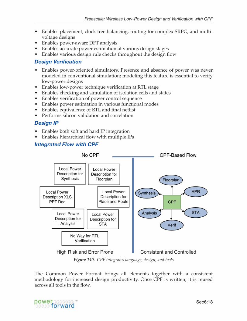
Enables placement, clock tree balancing, routing for complex SRPG, and multi-• voltage designsEnables power-aware DFT analysis• Enables accurate power estimation at various design stages• Enables various design rule checks throughout the design flow•
Design Verification
Enables power-oriented simulators. Presence and absence of power was never • modeled in conventional simulation; modeling this feature is essential to verify low-power designsEnables low-power technique verification at RTL stage• Enables checking and simulation of isolation cells and states• Enables verification of power control sequence• Enables power estimation in various functional modes• Enables equivalence of RTL and final netlist• Performs silicon validation and correlation•
Design IP
Enables both soft and hard IP integration• Enables hierarchical flow with multiple IPs•
Integrated Flow with CPF
Figure 140. CPF integrates language, design, and tools
Local PowerDescription XLS
PPT Doc
Local PowerDescription for
Place and Route CPF
Local PowerDescription for
Floorplan
Local PowerDescription for
Synthesis
Local PowerDescription for
Analysis
No Way for RTLVerification
Local PowerDescription for
STA
No CPF CPF-Based Flow
High Risk and Error Prone Consistent and Controlled
Floorplan
Synthesis
Analysis
APR
STA
Verif
The Common Power Format brings all elements together with a consistent methodology for increased design productivity. Once CPF is written, it is reused across all tools in the flow.

Freescale: Wireless Low-Power Design and Verification with CPF
Sec6:14
Mobile Application Power Reduction ResultsLow-power design techniques applied to a baseband processor for the cell phone to reduce standby power. During the sleep mode of the phone, the bulk of the baseband processor logic is in an idle state. A small portion of logic is awake to manage real time and associated functions. A low-frequency clock is dedicated to this purpose. All modules and subcomponents that do not use this low-frequency clock during sleep mode are prime targets for power management. A variety of techniques can be used to minimize the leakage in these modules. The following graph shows a sample power reduction exercise from a combination of power management techniques, including:
Reduced voltage• Device biasing• State retention power gating•
Good control of leakage is essential for managing the battery life.
Figure 141. Leakage reduction
1000900800700600500400300200100
0
9080706050403020100
Nominal SR/S&RPG/RV
SR/S&RPG
S&R PG
Techniques
C65 Leakage Reduction Example
Leak
age
Cur
rent
(uA
)
Bat
tery
Tim
e in
crea
se (%
)
SRPGAWBRV

Freescale: Wireless Low-Power Design and Verification with CPF
Sec6:15
SummaryEnergy efficiency is critical to today’s market needs. At Freescale, minimizing both static and active power is a competitive advantage, especially in mobile applications. CPF has enabled a consistent design flow for use of complex low-power techniques on large SoCs. Consistent representation, implementation, and verification through the entire design flow using CPF is an important need for productivity improvement and risk reduction. It is driving integration of all design tools for low-power.
Milind Padhye is Low-Power Design Manager at Freescale Semiconductor, Wireless design organization. He has been working in the field of low-power design for last six years and has multiple patents on power reduction techniques and integration. He has lead multiple chips for low-power architecture and design. Milind holds MS-EE from IIT Kharagpur, India in 1990.
