a progressive way to integrate current measurement into modern
TRANSCRIPT
A Progressive Way to Integrate Current Measurement into ModernPower Electronic Systems
Dr.-Ing. Martin SchulzInfineon TechnologiesWarstein, Germany
Email: [email protected]
Abstract
Modern inverter applications and sophisticated control schemes demand that the current flowing through theload is known exactly. Different measurement strategies can be utilized, each providing specific advantages anddisadvantages. Several possibilities are discussed in the paper presented and examined in detail with a focuson mechanical, thermal and electrical aspects. Of special interest is the possibility of higher integration and asolution is presented to achieve high accuracy current measurement with digital output and reinforced insulation.
1 Introduction
Current sensors are an inherent part of modern in-verter technology and need to fulfill different demandsdepending on the application. Besides costs the spaceneeded, the mounting technology utilized and the tem-perature range along with accuracy demands and re-sponse time are factors that influence the decision asto what sensor is to be used.An approach very common in inverter design is the useof current transducers as these components providesome obvious advantages. Sensors range from below1A to several kA. They can easily be mounted withoutintrusion regarding the wiring. Depending on the nec-essary response time Hall Effect sensors are availablein both open and closed-loop design with package sizesdown to SO8 for open loop transducers [1]. If howevershort circuit protection and short response times aremandatory, closed-loop systems need to be installed.Due to constructional reasons, these are larger in vol-ume and consume more space. One advantage of HallSensors is the galvanic separation they provide thoughin some cases it is a functional insulation only.A further magnetic field based current sensor is the socalled GMR. GMR means Giant Magneto Resistanceand refers to resistors that change their value accordingto a magnetic field applied. Build into a Wheatstonebridge, these sensors allow the measurement of cur-rents by measuring the magnetic field they cause. Thecomplete insulation and the size of the sensor itselfare advantageous. These devices, however, are sensi-tive to magnetic fields of any kind. Furthermore, if noadditional measures are taken, the polarity of the cur-rent is lost. Also detrimental is the fact that distanceto the wire, mounting position and angle between wireand sensor all influence the measurement.A more classical method to measure currents is usingshunts. The voltage drop across the shunt, caused bythe current to be determined, is measured. This so-
lution comes with the least expensive sensor but hastwo major disadvantages. The sensor does not providegalvanic separation and the resistor causes additionallosses. However, from new developments in the ar-eas of shunt technology, interconnection techniques,thermal management and signal processing circuitry itis necessary to reconsider shunts for current measure-ment in modern inverter designs.
2 Current Measurement in
Industrial Drives
Integrating current sensors into industrial drives usu-ally is done by mounting the sensor to PCB and addthe processing circuitry if necessary. While "off theshelf" Hall Effect sensors already contain the electronicto convert the measured signal into an analog signalwith scaled magnitude, this particular circuitry needsto be designed if shunts are used. Shunts can easily bemounted on PCB to measure currents in the range ofseveral amperes. The thermal situation gets difficult,however, if currents in a range of up to hundred am-peres occur. Due to the losses caused by the shunt inaddition to heat coming from power electronic devicesand from the PCB, temperatures beyond the level tol-erable for PCB materials could be reached. To preventthis from happening, it is mandatory to place shuntsin an area where the power losses can be dissipatedeasily. While mounting shunts to a heat sink leads toadditional wiring and additional space needed, includ-ing the shunts into a power module is an attractivealternative [2].
3 State of the Art
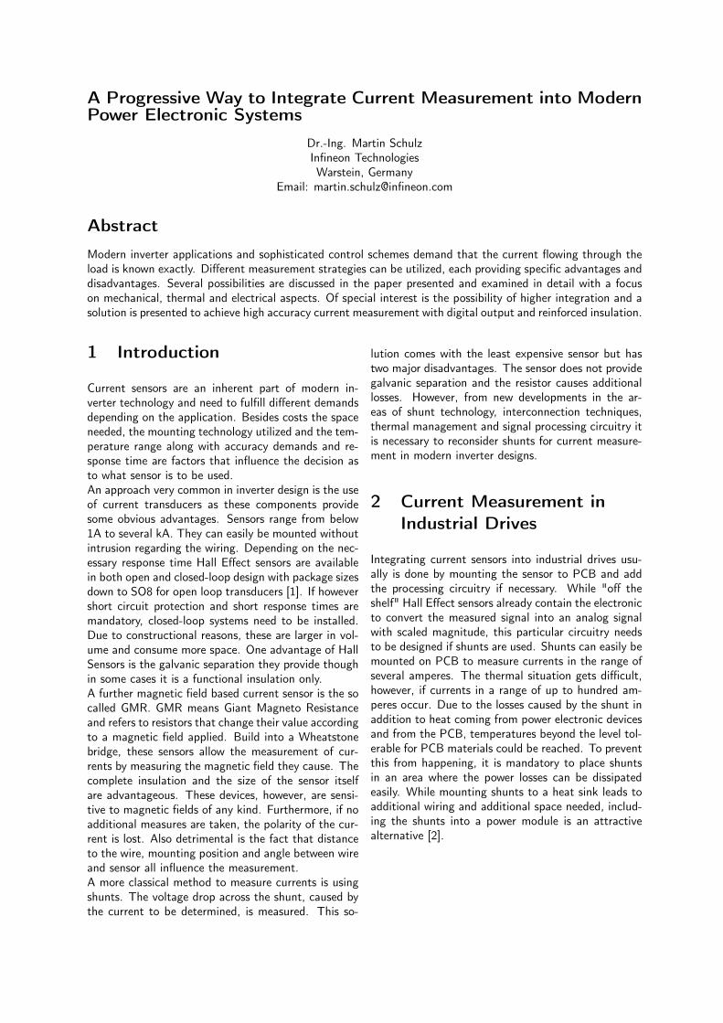
Today, IGBT-Modules like the FS75R12KE3_B3 forma full bridge with shunts in the output path. With avalue of 1.2mΩ the voltage drop at 75A is 90mV with adissipated power of 6.75W per output line. The shuntsused have a rectangular shape and in thermal aspectsbenefit from being soldered to DCB and module baseplate in a way similar to the IGBT and diode chips[4]. Though this is a well established technology itshows some noteworthy points that could be improved.From the shape and the size, the resistor used today iscomparable to the IGBT mounted inside the module.Thus, it also suffers from the same ageing effects. Asalso the soldering is similar, there is no possibility touse the area below the resistor. In conjunction with thebond wires necessary to contact the resistor’s surfacethe shunt consumes an area of approximately 10 ×
15mm2 as depicted in Fig. 1 below:
+
-
A
B
A B
Figure 1: 75A Bridge leg with shunt. Single ModuleDCB and schematic. Bonds to the shunt not shownfor clarity reasons.
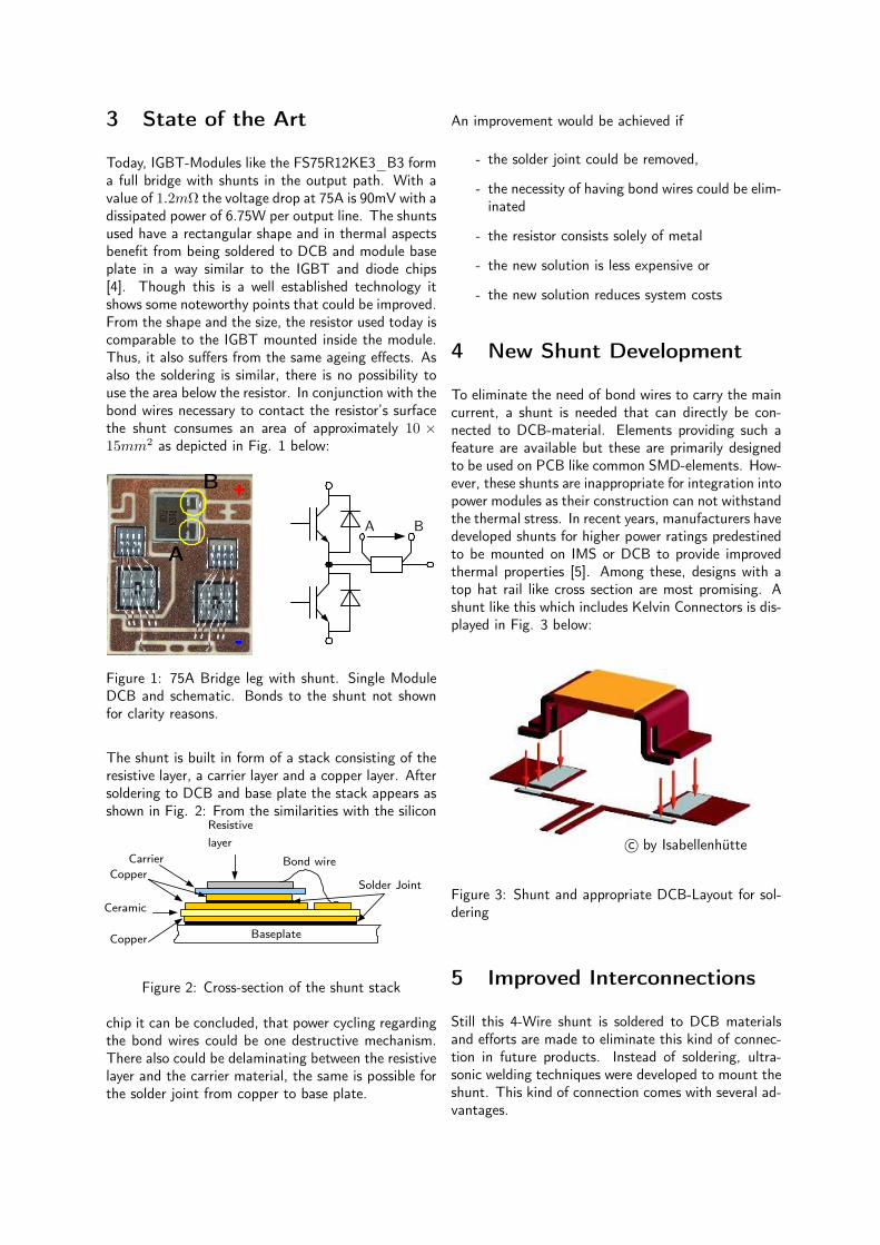
The shunt is built in form of a stack consisting of theresistive layer, a carrier layer and a copper layer. Aftersoldering to DCB and base plate the stack appears asshown in Fig. 2: From the similarities with the silicon
Copper
Copper
Ceramic
Carrier
Resistive
layer
Bond wire
Solder Joint
Baseplate
Figure 2: Cross-section of the shunt stack
chip it can be concluded, that power cycling regardingthe bond wires could be one destructive mechanism.There also could be delaminating between the resistivelayer and the carrier material, the same is possible forthe solder joint from copper to base plate.
An improvement would be achieved if
- the solder joint could be removed,
- the necessity of having bond wires could be elim-inated
- the resistor consists solely of metal
- the new solution is less expensive or
- the new solution reduces system costs
4 New Shunt Development
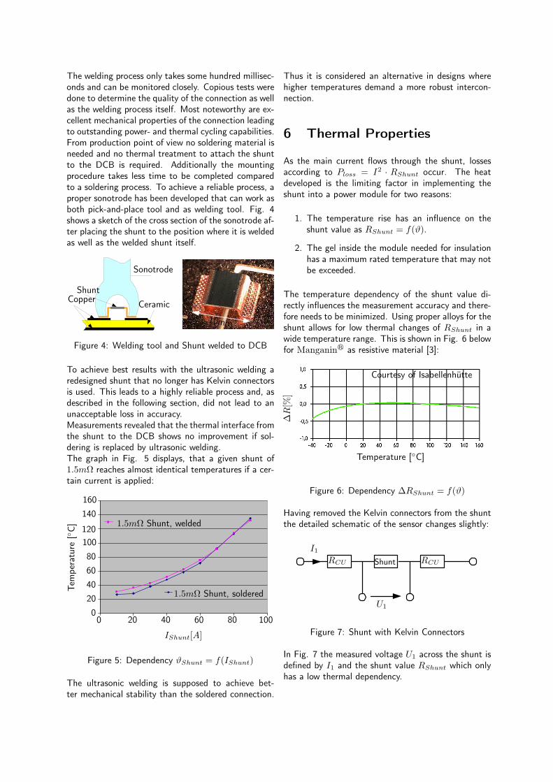
To eliminate the need of bond wires to carry the maincurrent, a shunt is needed that can directly be con-nected to DCB-material. Elements providing such afeature are available but these are primarily designedto be used on PCB like common SMD-elements. How-ever, these shunts are inappropriate for integration intopower modules as their construction can not withstandthe thermal stress. In recent years, manufacturers havedeveloped shunts for higher power ratings predestinedto be mounted on IMS or DCB to provide improvedthermal properties [5]. Among these, designs with atop hat rail like cross section are most promising. Ashunt like this which includes Kelvin Connectors is dis-played in Fig. 3 below:
c© by Isabellenhütte
Figure 3: Shunt and appropriate DCB-Layout for sol-dering
5 Improved Interconnections
Still this 4-Wire shunt is soldered to DCB materialsand efforts are made to eliminate this kind of connec-tion in future products. Instead of soldering, ultra-sonic welding techniques were developed to mount theshunt. This kind of connection comes with several ad-vantages.
The welding process only takes some hundred millisec-onds and can be monitored closely. Copious tests weredone to determine the quality of the connection as wellas the welding process itself. Most noteworthy are ex-cellent mechanical properties of the connection leadingto outstanding power- and thermal cycling capabilities.From production point of view no soldering material isneeded and no thermal treatment to attach the shuntto the DCB is required. Additionally the mountingprocedure takes less time to be completed comparedto a soldering process. To achieve a reliable process, aproper sonotrode has been developed that can work asboth pick-and-place tool and as welding tool. Fig. 4shows a sketch of the cross section of the sonotrode af-ter placing the shunt to the position where it is weldedas well as the welded shunt itself.
Copper
Shunt
Sonotrode
Ceramic
10mm
Figure 4: Welding tool and Shunt welded to DCB
To achieve best results with the ultrasonic welding aredesigned shunt that no longer has Kelvin connectorsis used. This leads to a highly reliable process and, asdescribed in the following section, did not lead to anunacceptable loss in accuracy.Measurements revealed that the thermal interface fromthe shunt to the DCB shows no improvement if sol-dering is replaced by ultrasonic welding.The graph in Fig. 5 displays, that a given shunt of1.5mΩ reaches almost identical temperatures if a cer-tain current is applied:
Tem
per
ature
[C]
IShunt[A]
0
20
40
60
80
100
120
140
160
0 20 40 60 80 100
1.5mΩ Shunt, soldered
1.5mΩ Shunt, welded
Figure 5: Dependency ϑShunt = f(IShunt)
The ultrasonic welding is supposed to achieve bet-ter mechanical stability than the soldered connection.
Thus it is considered an alternative in designs wherehigher temperatures demand a more robust intercon-nection.
6 Thermal Properties
As the main current flows through the shunt, lossesaccording to Ploss = I2 · RShunt occur. The heatdeveloped is the limiting factor in implementing theshunt into a power module for two reasons:
1. The temperature rise has an influence on theshunt value as RShunt = f(ϑ).
2. The gel inside the module needed for insulationhas a maximum rated temperature that may notbe exceeded.
The temperature dependency of the shunt value di-rectly influences the measurement accuracy and there-fore needs to be minimized. Using proper alloys for theshunt allows for low thermal changes of RShunt in awide temperature range. This is shown in Fig. 6 belowfor Manganinr as resistive material [3]:
Temperature [C]
∆R
[%]
Courtesy of Isabellenhütte
Figure 6: Dependency ∆RShunt = f(ϑ)
Having removed the Kelvin connectors from the shuntthe detailed schematic of the sensor changes slightly:
RCURCU Shunt
I1
U1
Figure 7: Shunt with Kelvin Connectors
In Fig. 7 the measured voltage U1 across the shunt isdefined by I1 and the shunt value RShunt which onlyhas a low thermal dependency.

In Fig. 8 however, the temperature dependency ofthe copper connectors adds to the shunt leading to ameasured voltage of U2 = I2(2 · RCU + RShunt).
RCURCU Shunt
I2
U2
Figure 8: Shunt without Kelvin Connectors
From the shunt geometry the value RCU can be calcu-lated to be 11µΩ at 20C. With a linear temperaturecoefficient αCU = 0.0039 1
Kthe value changes from
11µΩ at 20C to 18.7µΩ at 200C adding a totalof 37.4µΩ to the shunt assuming that all the copperreaches 200C. Observing the shunts operating condi-tions using a thermographic camera provides an insightinto the quality of the connection proposed in this pa-per. Fig. 9 shows the shunt attached to a DCB on anEcono3 base plate and mounted to a proper heatsink:
Figure 9: Thermographic picture of the shunt duringoperation, outline drawn for better overview
The picture is taken with a temperature of 150C inthe center of the shunt and 40C on top of the DCB. Inan application, the base plate temperature is expectedto reach 85-100C leading to a temperature level ofup to 115C for the position the shunt is mounted in.With maximum 200C allowed for the shunt itself, thecopper resistance added to the shunt under these con-ditions is about 34µΩ.
Using a shunt with a nominal value of 2400µΩ will leadto 2422µΩ at 20C including the copper and 2434µΩat 200C resulting in an increase of less than +0.5%which is, due to the thermal properties of Manganin,almost compensated for.
7 Galvanic Separation and
Signal Processing
Even with the thermal situation improved the maindisadvantage of the shunt remains its lack of galvanicseparation. However, any equipment that connectsthe shunt to a microcontroller needs to be designed ina way that it separates control and power electronics.One common way to do so is to have the voltage acrossthe shunt digitized using an A/D-converter that has itssupply voltage referenced to the high side voltage. TheA/D’s digital information is then passed to the con-trol by means of optocouplers. As optoelectronic ele-ments are known to age under high temperature, a fur-ther step of optimization would be to improve on thismethod of transmission. Here, the coreless transformertechnology that is already in use in IGBT-Drivers [6] iscombined with Sigma-Delta data conversion technol-ogy forming an interface to the sensor. The task to becompleted by this interface is to read out the electricvalue, transform it to digital information and transmitthis information to the controller level providing rein-forced insulation. The schematic for one bridge legwith shunt, high side driver and sigma delta converterboth based on coreless transformer technology looksas shown in Fig. 10
Gate-
signal
+5V
+5V
Shunt
Outp
ut
Logic
Logic
Insula
tio
n
Insulation
Drive
r Σ/∆
1EC010I12-S
1ED020
UCC
Figure 10: Bridge leg with shunt, Σ/∆-Converter andhigh-side IGBT driver
As can be seen, the supply voltage UCC provided tothe driver is the same as the one supplying the con-verter, the +5V needed for the logic are identical tothe microcontroller’s supply. The insulation achievedby using the Coreless Transformer technology qualifiesas reinforced insulation.
8 Measured Results
A system as shown in Fig. 10 was first set up in thelaboratory to evaluate the measurement. The step re-sponse from I = 0 to I = INom was recorded using aLeCroy current probe AP015 and the Σ/∆-Converterproposed.

The result is displayed in Fig. 11, the current to bemeasured was turned on at t = 0. A resolution cor-responding to 16bit was chosen. This in combinationwith the 10Mhz sampling rate leads to 6.4µs betweentwo samples. As a sinc3-filter [7] was used in the setup,three steps of delay appear as expected. The finalvalue is approximated within 6 cycles or 38.4µs.
−50 −25 0 25 50 75
Time[µs]
Σ/∆-Output Current
Curr
ent
Ratio
I/I N
om
−0.20
0.20.40.60.8
11.21.4
Figure 11: Measured Step Response
It is a feature of the sigma-delta technology that thebit rate can be chosen according to the application’sneeds. Lower resolution results in faster response butin less accurate measurements as well. Higher resolu-tion provides the more accurate measurement but alsoincreases measurement time. For a modern inverterapplication it is necessary to determine the instanta-neous value of the current within a time correspondingto the inverter’s switching frequency. For motor driveapplications, this frequency today is up to 20kHz so aresponse time of the measurement equipment of 50µsis sufficient for current control. To be used as a shortcircuit detection, response times ¿ 10µs are manda-tory. Though this can not be achieved in form of ameasurement, the sigma-delta-technology provides a"workaround". An initial estimate is done in the con-verter’s decimator parallel to the real measurement. Ifthis estimation detects an overcurrent a special signalis generated allowing the user to determine a properaction. In the given example this signal is availableabout 2.8µs after the short circuit occurs. The ac-cording correlation is shown in Fig. 12
−3 −2 −1 0 1 2 3 4
Time[µs]
Current Ratio SC-Detection
Curr
ent
Ratio
I/I N
om
SC-D
ete
ction
0
1
0
1
2
3
4
Figure 12: Short Circuit Detection
9 Conclusion
New shunts, new interconnection techniques and newsignal processing technologies can be combined to forma highly accurate, cost saving current measurement.Improvement also is achieved in thermal design andspace requirements due to the integration of the sensorinto the power module. Reinforced insulation is pro-vided by coreless transformer technology. The mea-surement presented in this paper can provide accu-rate data for regulation purpose as well as informationto handle overcurrent situations. Shunt based currentmeasurement remains a very attractive solution for awide range of power electronic systems.
References
[1] A. Friedrich,New Applications for Hall-Effect Cur-
rent Sensors,Bodo’s Power Systems Sept. 2006,pp. 38 - 39
[2] U. Hetzler, K. Göpfrich, R. Stark, Paradigmen-
wechsel bei Frequenzumrichtern, Strommesswider-
stände statt Stromwandler, Germany, electronikindustrie 1/2 -2005
[3] Flyer SMD-Shunts für Hochstromanwendungen,Germany, Isabellenhütte, May 2005
[4] M. Hornkamp, Current Shunt Resistors integrated
in IGBT Power Modules for Medium Power Drive
Application, PCIM-China 2004
[5] Datasheet, Isabellenhütte, ISA−WELDr SMD
precision resistors
[6] Datasheet, Infineon Technologies,EiceDRIVERTM1ED020I12-S Single IGBT Driver
IC
[7] R. Kusch, Decimation Lowpass Filter for Sigma-
Delta Modulators, Hamburg, Diplomica GmbH,2002