a publication of the microelectronics packaging & test
TRANSCRIPT

Book-to-Bill RatioFORNOVEMBER 1.00
MEMBER COMPANY PROFILE
Heraeus has been the leading manufactur-er of materials for assembly and packag-ing technology in the electronics industry for the last 40 years. Heraeus Contact Material Division meets all applicable industry standards including ISO 9001 certification. With state of the art manu-facturing and clean room facilities located around the world in locations including the USA, Germany, China, France, Korea, and the Philippines Heraeus is situated to support and service customers on a global basis. page 10
Semiconductor equipment bookings decrease 4% over October 2008 level. page 16
F or over 150 years Heraeus has been at the forefront of materials technology devel-opment. As a global company
with more than 11,000 employees, Heraeus has the reach to support customer operations on a worldwide basis. With dedicated teams of R&D and Application professionals, Herae-us works with customers to develop cutting edge products that enable customer designs and applications.
A Publication of The MicroElectronics Packaging & Test Engineering Council
One Day Technical Symposium and Exhibits Coming to San Jose, CA February 19th ... page 4
www.meptec.org Q4 2008 / MEPTEC Report 1
INDUSTRY NEWS
Centipede Systems is partnering with TopLine to provide test users with a new, cost-effective test evaluation tool. page 12
Amkor has announced that ASAT Holdings Lim-ited has entered into an agreement to license Amkor’s FusionQuad® package technology.page 13
Quik-Pak has announced the acquisition of Aguila Technologies’ flip chip assembly, detec-tor array processing, and laser micromachining business units. page 14
TechSearch International’s new study, 2008 Flip Chip and WLP Market Trends and Fore-casts, projects a compound growth rate of more than 14 percent for flip chip units and 14 percent for WLPs between 2007 and 2012.page 17
Volume 12, Number 4
QUARTER FOUR 2008
Semiconductor Packaging Impacting the Age of Consumer Electronics
The Pan Pacific Microelectronics Symposium and Tabletop Exhibition, sponsored by SMTA, will be held February 10-12 at the Hapuna Beach Prince Hotel, Hawaii. page 8

the right fit
Contact Honeywell for solutions to your puzzle…visit www.honeywell.com/sm/em or call 1-408-962-2000.
© 2007 Honeywell International Inc. All rights reserved.
With the right investments in the right places at the right time, we’re uniquely positioned to help you make the connection from idea to product success.
Honeywell’s ongoing research and development in chemistry,
metallurgy, and the processes that bring them together—from
our new packaging R&D facility in Spokane, Washington, to our
technology center in Shanghai, China—ensure that wherever challenges arise, we’ll continue
to create solutions that solve them. And as a partner to most of the top semiconductor
houses worldwide, our technology portfolio is consistently at the forefront of invention,
empowering the global leaders of innovation. Honeywell Electronic Materials—bridging
the path to accelerated success.
Right Fit-MR-Q407.indd 1 11/12/07 2:00:45 PM

W e at MEPTEC are probably not the only ones to breathe a sigh of relief that 2008 is over. It’s been a rocky and uncertain year, and the optimis-tic view is it can only get better. Our
industry has weathered bad times before; we’ll get through this one as we have before, and be stronger for it. In the meantime as we’re working towards improvement, MEPTEC will be moving forward, just as we have the last 30 years, to continue to bring you our high quality services which include our popular technical programs, as well as networking and marketing opportunities. We also have some new programs in development that you’ll be hearing about soon. MEPTEC’s next event will be held on February 19 and is titled Semiconductor Packaging: Impact-ing the Age of Consumer Products. This event will be very timely in that it will cover, among other things, topics that address the all important bottom line. Sessions will cover time-to-market and pack-aging for consumer products; cost-of-ownership challenges; solutions for consumer products minia-turization, and advancing technologies for consumer products. Exhibits and sponsorships are available. See page 4 for further information. Our Industry Analysis this issue is from the pro-digious Jan Vardaman. She is not only prodigious, she is ubiquitous as well. She does so many things for MEPTEC, such as speaking and writing articles, and we know she does that for many other organiza-tions as well. On page 5 Jan discusses something I think we’re all happy to hear about, and that’s a “bright spot” in our industry. That bright spot is Progress in Flip Chip Technology. She explains developments in the area of flip chip, such as in bumping, flip chip substrates, and assembly servic-es. She concludes by saying that although consumer products may slow in 2009, growth will continue to be seen in the area of advanced packaging, including flip chip interconnect. We’re covering the University of Bridgeport in our University News section this issue. In Opening Doors, Building Futures, the article describes the many course areas that will help bring our indus-try some of newest, best and brightest engineers, including VLSI, NEMS/MEMS, signal processing and Biomedical Engineering. The University is also currently developing programs in the areas of Energy and Power and Machine Control. See page 9 for their story. Our Company Profile this issue is from MEPTEC Corporate member Heraeus. It focuses
on their Contact Materials Division which was formed 40 years ago. It’s a relatively “new” divi-sion considering Heraeus has been in existence for over 150 years. In the Profile, the Contact Materials Division’s products and technologies are described. With their continued innovation in materials, it’s likely that they’ll be around at least another century and a half! We appreciate Heraeus’ continued sup-port of MEPTEC. See their story on page 10. Our first feature article is from MEPTEC mem-ber and entrepreneur Peter Salmon of Salmon Technology LLC. Peter describes a new technology for Solder-Free Connectors Using Buckled Pillars (see page 18). He talks about possible replacements of existing packaged devices, how and why this new technique will work, cost tradeoffs and chal-lenges. He summarizes by explaining the versatility and adaptation of the technique to many different substrates and chip stack configurations. Thanks to Peter for this informative article. Our next feature article is from another long-time MEPTEC member, Hestia Technologies. Hal Shoemaker and Pat Weber describe a new molded underfill process which allows for over mold and underfill at the same time with the same mold com-pound. They explain how using this new technology can lower costs – something that’s of interest to most of MEPTEC’s member companies these days. See page 20 for the article. Our Editorial this issue is very interesting and timely. In Medical Automation: Fueling the Demand and Increasing the Complexity of Electronics Pack-aging, Dr. Robin Felder, Ph.D. at the University of Virginia gives a very compelling look at how auto-mation could improve the health care industry, not to mention saving potentially billions of dollars in the process. He explains how the healthcare industry has lagged behind almost all other industries in the U.S. when it comes to automation. The advancements in devices and processes he describes are mind-blow-ing. In his conclusion, Dr. Felder says that “Elec-tronic design and packaging is the fundamental basis for this technological revolution in health care”. With the fast growing biomedical industry, those of us in packaging must stay informed of these devel-opments, and participate in the automation that will help streamline the delivery of healthcare. We’d like to thank all of our contributors for making this a great issue. If you’re reading our pub-lication for the first time at one of the many events where we distribute, or if you’re a new member, we hope you enjoy it. Thanks for joining us! ◆
Council UpdateVolume 12, Number 4
A Publication of The MicroElectronics Packaging
& Test Engineering Council
P. O. Box 222Medicine Park, OK 73557
Tel: (650) 714-1570 Email: [email protected]
Published ByMEPCOM
EditorBette Cooper
Design and ProductionGary Brown
––––––––––––––MEPTEC Advisory Board
Seth AlaviSunSil
Jeffrey BradenLV Sensors, Inc.
Philippe BriotP. Briot & Associates
Joel CamardaGTronix
Gary CatlinPlexus
Tom Clifford
Rob Cole
John CraneJ. H. Crane & Associates
Jeffrey C. DemminTessera
Bruce EuzentAltera Corporation
Skip Fehr
Julia GoldsteinAdvanced Packaging Magazine
Anna GualtieriElle Technology
Bance HomConsultech International, Inc.
Ron JonesN-Able Group International
Nick LeonardiPremier Semiconductor Services
Phil MarcouxTPL Group
Bhavesh MuniHenkel Corporation
Mary OlssonGary Smith EDA
Marc PapageorgeSemiconductor Outsourcing Solutions
Mike PinelisMEMS Investor Journal
Rich RiceASE (US) Inc.
Jim WalkerGartner Dataquest
Russ WinslowSix Sigma
––––––––––––––
MEPTEC Report Vol. 12, No. 4. Published quarterly by MEPCOM, P. O. Box 222, Medicine Park, OK 73557. Copyright 2008/2009 by MEPTEC/MEPCOM. All rights reserved. Materials may not be reproduced in whole or in part without written permission.
MEPTEC Report is sent without charge to members of MEPTEC. For non-members, yearly subscriptions are avail-able for $75 in the United States, $80US in Canada and Mexico, and $95US elsewhere.
For advertising rates and information contact Gina Edwards at 408-8585493, Fax Toll Free 1-866-424-0130.
www.meptec.org Q4 2008 / MEPTEC Report 3
MEPTEC Welcomes New Advisory Board MemberMike Pinelis is the CEO and editor of MEMS Investor Journal, an independent publication he founded in 2003 and grew to the current 3,600+ subscribers worldwide. Along with MEMS Investor Journal, he has also developed a management consulting and recruiting practice focused on MEMS, sensors and microsystems. Prior to MEMS Investor Journal, Mr. Pinelis served as Director of Business Development for ISD Technology Group in Mansfield, Massachusetts. Prior to that, Mr. Pinelis founded MindCruiser, a company specializing in developing intellectual property online marketplaces that was sold to Akiva Corporation in 2001. Mr. Pinelis earned a bachelor’s degree in electrical engineering from Harvey Mudd College in Claremont, California and a master’s degree in electrical engineering with a focus in MEMS and microfluidics at the University of Michigan in Ann Arbor where he is currently a PhD candidate. ◆

R E G I S T E R O N L I N E T O D A Y A T M E P T E C . O R G
A O N E - D A Y T E C H N I C A L S Y M P O S I U M & E X H I B I T S
MEPTECPRESENTS
Semiconductor Packaging Impacting the Age of Consumer ElectronicsFebruary 19, 2009Wyndham Hotel • San Jose, California
MEDIA SPONSORS
C onsumer electronic products have firmly established a powerful role in driving the further evolution and growth of the semiconductor packaging industry. Device complexity continues to increase, as does demand for extreme miniaturization,
lower cost, higher performance, and unprecedented package level integration of con-trasting device functions.
Today, chipmakers are scaling down their devices to create faster, more efficient and more portable consumer electronics. The packaging industry is paving the way forward by creating new, innovative package configurations featuring a combination of flip chip and wire bond interconnection, buildup and laminates substrate technology, as well as complex integration schemes based on combinations of 3-D package stacking.
Keynote Speaker Ronald Steger, Partner-in-Charge of Global Semiconductor Practice of KPMG. KPMG recently co-conducted a study with GSA (Global Semiconductor Association) and the CEA (Consumer Electronics Asso-ciation) on The Consumer Electronics Boom: How Semi-conductor and Consumer Electronics Companies are Im-proving Cost, Time-to-Market and Product Quality.
Sessions will include:
n Time-to-Market and Consumer Semiconductor Packaging
n Cost-of-Ownership Challenges for Consumer Products
n Solutions for Consumer Products Miniaturization
n Advancing Technologies for Consumer Electronics
GOLD SPONSOR
SILVER SPONSOR

MEPTEC Industry Analysis
P rospects for the growth of flip chip interconnect is being seen as a bright spot in the electronics industry. An increasing number of
companies are expanding the use of flip chip with solder bumps and copper pillars in packages. This includes sup-pliers of ASICs, field programmable gate arrays (FPGAs), DSPs, chipsets, graphics, and microprocessors. Figure 1 shows an assortment of Fujitsu’s flip chip packages for high-performance applications. The limiting factor in the greater expansion of flip chip has been the shortage of laminate sub-strates, but this situation has improved dramatically with the increased capac-ity. The use of flip chip for a variety of wireless products will contribute to continued growth in 2009. Many of today’s new packages incorporate a flip chip bumped device, includ-ing package-on-package, stacked die packages, and single chip packages. Figure 2 shows the use of flip chip in the bottom package of Amkor’s PoP. While most of the growth will be in flip chip in package (FCIP), flip chip on board (FCOB) continues to be found in automotive electronics, hard disk drives, and watch modules [i]. Gold bumped devices continue to be used for display drivers as chip-on-glass (COG), chip-on-film (COF), and tape automated bonding (TAB) methods. Bumped die, including dis-play drivers with gold bumps, solder bumps and copper pillar, account for approximately 6 percent of IC ship-ments.
NEW BUMPING DEVELOPMENTS
Flip chip in the form of solder bumps or copper pillar, represents approxi-mately three percent of IC shipments today. Many companies are using Pb-
free solder bumps, regardless of the status of RoHS exemptions. The rea-sons for implementation include cus-tomer requests, competitive pressure from Intel’s switch to Pb-free, and the desire to convert technologies before a RoHS mandate. In some cases, cus-tomers prefer Pb-free bumps when alpha emissions are a concern. Almost all bump suppliers offer Pb-free solu-tions. While many assembly issues in the adoption of low-k dielectrics have been addressed, the use of Pb-free solder with low-k and ultra low-k dielectric remains a concern.
Many companies are investigating the future use of copper pillar. Intel selected the copper pillar because it is a reduced Pb-content solution that offers better thermal performance, improved electrical conductivity, and resistance to creep and electromigra-tion, compared with conventional
solder. Additional advantages include lowering the bump critical dimension floor, and continued downward scal-ing of the passivation opening size, extensions to higher I/O densities. The copper pillar process also provides options for tighter silicon and package routing pitches that can lead to higher pin densities and reduced die sizes. The copper die bumps allow the use of a simplified under bump metallization (UBM) [ii,iii]. Infineon has conducted extensive analysis of the copper pillar for wireless applications. Copper pil-lar process has some issues that must be considered. The copper patterning process requires a thick photoresist because the bumps do not undergo reflow to attain their final geometry.
Micro bumps or ultra-fine-pitch flip chip bumping is defined as having a bump pitch of 60 µm or less. A micro bump is sometimes used with chip-
Progress in Flip Chip Technology: Today’s Bright Spot E. Jan Vardaman PresidentTechSearch International, Inc.
Figure 1. Fujitsu’s ASICs in Flip Chip Packages Source: Fujitsu
www.meptec.org Q4 2008 / MEPTEC Report 5

MEPTEC Industry Analysis
6 MEPTEC Report / Q4 2008 www.meptec.org
on-chip (CoC) technology and several companies plan to use it with through silicon via (TSV) technology. Many research institutes are developing a variety of processes and several com-panies show the technology on their roadmaps, but for most it is still in the development stage. Sony has one of the few production examples, used in a PlayStation.
Gold stud bump or stud bump bonding (SBB) has been used for many years by Japanese and European compa-nies, and the volumes are increasing as additional companies adopt the technology due to the extremely fine pitch it offers. Gold stud bump is used for stacked die packages found in mobile phones and in consumer products such as digital cameras and camcorders. The technology is also used in hearing aids, high brightness LEDs, SAW filters, and some automo-tive applications.
FLIP CHIP SUBSTRATES
Silicon substrates for flip chip applica-tions have been developed by IBM, Infineon, NXP, STMicroelectronics, and others. NXP developed the Pas-sive Integration and Connecting Sub-strate (PICS) process that incorporates integrated passives in the substrate. Flip chip devices such as a transceiver and a power amplifier are mounted on the substrate that contains the integrat-ed passives. STMicroelectronics ships RF applications such as Bluetooth and wireless LAN using flip chip interconnect. Transceiver modules use its integrated passive device (IPAD) technology (a thin-film-on-glass sub-strate) with flip chip die [iv].
Laminate substrate will continue to move to higher density and thinner cores as the industry moves to the next
node of semiconductor technology and bump pitch decreases. Substrate core thickness is expected to decrease. The industry has already adopted via-in-pad for some applications. Laser via stack and core via stack will also be adopted.
ASSEMBLY SERVICES
As the distinction between board-level assembly and IC package assem-bly becomes less clear, the flip chip assembly services industry becomes more difficult to segment. Assembly of flip chip packages can be provided by either an IC package service pro-vider or a board-level assembly house, especially for system-in-package (SiP) or multichip packages. More than 40 companies offer assembly services for flip chip interconnect in IC packages or on boards or modules. Flip chip bumps may be solder, copper pillar, gold, or stud bumped. Substrates may be flex circuit, glass, ceramic, lami-nate, or thin-film.
CONCLUSIONS
Technical and infrastructure barriers to the adoption of flip chip have been removed as the industry has matured. The expansion of flip chip technol-ogy for many applications has been limited because its cost exceeds that of conventional wire bonding. New bumping technologies continue to be introduced for the flip chip market, including copper pillar technology and an injection mold process devel-oped by IBM and commercialized by Suss. These developments were driven in part by European legislation banning lead from electronic assem-blies. Today, most companies have qualified Pb-free bumping solutions, even though some exemptions remain. Also, the assembly of bumped silicon fabricated with low-k dielectric mate-
rials and Pb-free bumps will require additional changes to the materi-als and to the assembly process and drive greater emphasis on co-design. Demand is increasing for solder, cop-per pillar, WLP, and gold bumping on 300mm wafers.
The economic decision of flip chip versus wire bond is being made on a case-by-case basis. While slower growth in products such as personal computers and consumer products in the first half of 2009 may dampen semiconductor growth rates in general, the demand for increased functional-ity, form factor, and performance will continue to drive growth in advanced packaging, including flip chip inter-connect. ◆
References
[i] E. J. Vardaman, et al., “2008 Flip Chip and WLP Market Trends and Forecasts,” TechSearch International, Inc., September 2008.
[ii] A. Yeoh, et al., “Copper Die Bumps (First Level Interconnect) and Low-K Dielectrics in 65nm High Volume Manufacturing.” Electronic Components and Technology Confer-ence, May 2006.
[iii] “Copper Pillar Bumping in Intel Microprocessors”, Andy Longford and Dick James, Semicon Europa 2006.
[iv] E. J. Vardaman, “New Develop-ments in Flip Chip,” VLSI Packaging Workshop, Kyoto, Japan, December 2008.
Figure 2. Flip Chip in Bottom Package of PoP. Source: Amkor

SemicoSUMMIT09_Ad.pdf 11/20/08 10:46:44 AM

SPONSORED BY
www.smta.org | 952.920.7682 | [email protected]
SMTASurface Mount Technology Association
10 - 12 February 2009Hapuna Beach Prince Hotel | The Big Island of Hawaii
Microelectronics Symposium and
Tabletop Exhibition
Microelectronics Microelectronics 2009
14TH ANNUAL
The Pan Pacifi c Symposium focuses on the critical business markets and technologies of microelectronic packaging, interconnection,
microsystems technology and assembly.
The Pan Pacifi c Tabletop Exhibition puts you in contact with global key decision makers and provides access and international visibility
for your company and products.

T he Electrical Engineering Depart-ment at the University of Bridgeport has 4 major areas or concentrations. In addition to the courses listed, students can gain a more intense
learning of each area by doing a senior project, master’s project, or thesis (MS or PhD).
The EE department’s first area, VLSI (very large scale IC design), offers a dozen courses that are either VLSI or VLSI-related: low power VLSI, Analog VLSI, VLSI testing, Radio frequency VLSI, digital and introduc-tory VLSI as well as courses in nanotechnol-ogy, microfabrication, semiconductors, FPGA design, digital IC design electronics, and ana-log IC design electronics. There are 4 full-time and one part-time Faculty teaching and doing research in this area. Some examples of proj-ects/theses done in this area include mixed signal chip design, power optimization at RF, memory versus speed for alternate design technologies of the same function, and others. They have EDA tools as well as up-to-date versions of Pspice, Xilinx, Synopsys, Mentor Graphics, Labview, Matlab, Ansys, etc. In the second area the NEMS/MEMS (nano- and micro-electromechanical systems) program introduces the future technologies that apply to even smaller computers and very tiny medical devices, as well as ever smaller devices in a host of disciplines, including Fiber Optics and Signal Processing. Devices of one millionth or one billionth of a meter have the capability of providing high densities of intelligence in a package of extremely small size and power. The courses in this program include: MEMS, Introduction to Nanotech-nology, Microelectronic Fabrication, Medical Electronics, Fiber Optics, and a host of VLSI courses. Recent projects/theses include mems
comb accelerometer, torsional mems micro-positioning mirrors, mems gyroscope, Bio-mems sensors. Design tools include Ansys, Pspice, Autocad, and Mentor Graphics. Thirdly, the SP (signal processing) area teaches the analysis, interpretation, and manipulation of data from a diverse set of sources, including: biological signals, radar, images, sound, and fiber optics. Processing is both analog/digital/discrete for light waves, radio waves, sound waves, and images, both functional and biological. Processing includes filtering, storage, reconstruction, compression, and noise abatement. Courses include sev-eral in speech processing, digital processing, lightwave processing, RF, and microwaves.
Labs to complement each of these courses are in place as well. Students make extensive use of Matlab. Labs use chips from various vendors, especially Texas Instruments. Astro-nomical signal processing is being added to this area, including data collected from off-campus observatories dealing with sunspots and variable stars. Further developments in Medicine are being added to their program as new experiments; these include analysis of ECG and EEG data. The department’s fourth area, their Bio-medical Engineering area, is actually a fully licensed program that has just begun. Many Biomedical courses are already in place, hav-ing been started years earlier as Electrical Engineering courses: Medical Machines, Bio-Signal processing, Biosensors, Bioinformat-ics, and Biomaterials. This area will accept its first class in the Fall of 2009. This can be broken down into 3 tracks: Biomaterials, Bio-
instrumentation, and Bio-computer science (such as Bioinformatics). The graduate of this program will obtain the MS, and she or he will have a proficiency in mathematics, tech-nology management, biology, and biomedical courses in Electrical Engineering. BioSignal processing is a 4th track that depends on the prior 3 and focuses on the signals produced by medical machines (ECG, EEG, pulse ox, MRI, etc.) and the analysis thereof. The University also has developing areas in (i) Energy and Power and (ii) Machine control. The former includes courses in the generation of power by conventional and non-conventional means. The latter includes Programmable Logic Control and Industrial control of heavy machines as well as Robotics. There is movement to have a licensed degree in Energy and Power, just as they now have a licensed degree in Biomedical Engineering. For more information about the University of Bridgeport and their Electrical Engineering programs visit www.bridgeport.edu. ◆
MEPTEC University News
UNIVERSITY OFBRIDGEPORT Opening doors. Building futures.
www.meptec.org Q4 2008 / MEPTEC Report 9
There are currently nine masters students work-ing on their M.S. project/thesis and independent study under Professors Syed Rizvi and Khaled Elleithy. Students presented the research status of their work in the University of Bridgeport’s Wireless and Mobile Comminications Lab.

MEPTEC Member Company Profile
10 MEPTEC Report / Q4 2008 www.meptec.org
E lectronic technology has signifi-cantly influenced modern society. For over 150 years Heraeus has been at the forefront of materi-als technology development. As
a global company with more than 11,000 employees, Heraeus has the reach to support customer operations on a worldwide basis. With EUR 12 billion in sales and dedi-cated teams of R&D and Application profes-sionals, Heraeus works with customers to develop cutting edge products that enable customer designs and applications. During the last 40 years the Contact Materials Division of Heraeus has been the leading manufacturer of materials for assembly and packaging technology in the electronics industry. Heraeus Contact Mate-rial Division meets all applicable industry standards including ISO 9001 certification. With state of the art manufacturing and clean room facilities located around the world in locations including the USA, Germany, China, France, Korea, and the Philippines Heraeus is situated to support and service customers on a global basis.
PRODUCTS
Solder Paste Solder pastes designed for applica-tions such as Surface Mount Assembly, SiP Assembly, Wafer Bumping and a range of other applications are available. These prod-ucts are available in a variety of versions including No Clean, Lead Containing, Lead Free, RoHs Compliant, REACH Compliant, RMA, and Water Soluble. One of the critical constitutes of solder paste is the solder pow-der. Heraeus produces its own powders thru its PSP and Welco operations and utilizes specialized technology which allows for the high quality production of powder sizes ranging from Type 3 to Type 8. This capabil-ity allows Heraeus to be at the forefront of technology as devices are miniaturized and feature increased functionality.
Fluxes Fluxes have been developed for a wide range of applications such as chip attach, component balling, and rework. Fluxes are liquid, paste or gel based to ensure compat-ibility with deposit techniques which include spraying, foaming, dipping, pin transfer, and dispensing. Additionally, fluxes are available in no clean and water soluble chemistries to
ensure the lowest level of false rejects during pin testing and compatibility with underfill processes.
Adhesives Heraeus also features a complete line of adhesive products which include conduc-tive adhesives, non conductive adhesives, SMT adhesives, and thermally conductive adhesives. This wide range of products can be applied by several processes including dispensing, jetting, printing, and pin transfer. Non conductive adhesives feature cure times from 10 seconds to 90 minutes at tempera-ture from 80˚C to 180˚C. They also feature high shear strength and excellent reliability characteristics. Conductive adhesives are used for die and component attach to sub-strates, ceramics, LTCC, leadframes, flex circuits, and many other applications. These adhesives also feature a wide range of curing schedules and excellent reliability. Major uses include the assembly of dies and com-ponents to substrates for high temperature automotive applications and such as engine control modules, gear control units, and safety equipment.
Spheres Heraeus solder spheres are characterized by smooth, clean surfaces and tight size distribution. Additionally the spheres feature
a very low oxide level and are thus very stable during long term storage. Spheres are produced in sizes from 500 µm to 50 µm at the companies PSP operation and are
Contact Materials DivisionHeraeus
SMT Technology Center
Measurement of Wafer Bumping Pastes
Heraeus Product Line

produced using a fully automatic manufac-turing process. This enables spheres to be produced with exceptional consistency and a Cpk > 1.33. The uniform microstructure and the well controlled surface oxidation level ensures reliable performance in all processes.
Bonding Wire Heraeus is also a major supplier of bond-ing wires, ribbon, and specialty wire. Based on gold, copper, palladium, and aluminum with diameters extending into the micron range these wires are suitable for a wide variety of semiconductor applications. Gold wire is produced from ultra pure starting materials with doping additives to improve performance characteristics. All wires are corrosion resistant and display homogeneous chemical composition and stable mechanical properties. Gold wires feature excellent loop stability and flat loop geometries along with high thermal stabil-ity. Aluminum bonding wires are utilized where low processing temperatures are required and are typically used for auto-motive and power applications. Addition-ally, they can be alloyed with magnesium to improve fatigue strength properties. Alu-minum wires have excellent mechanical properties and high strength. Copper wires are formed using a high purity copper matrix and achieve excellent processing properties by means of defined addition elements. Copper wires have very stable mechanical properties and a highly reliable bonding joint. Copper wires feature high conductivity and high tensile strength with high elongation properties. Addition-ally, the wires exhibit reduced formation of intermetallic phases.
INNOVATION Innovation is a key to long term survival and a key to Heraeus more than 150 years of Industry Leadership. An example of this is the recently released Ball Dip series of pastes. This product line was one of three recipients of the 2007 Heraeus Innovation
Prize and has been instrumental in improv-ing process yield for component assemblers. Despite the tackiness offered by ball attach fluxes, they have failed to prevent ball movement on solder on pad finishes when the solder protrudes above the sol-der mask. Solder bridging and joined balls become a common occurrence prompting heavy rework of units. Rework lengthens the manufacturing cycle time and poses a product reliability risk. The same ball movement plagues ENIG pads on FC ceramic substrates. These solder ball pads do not provide a solder mask edge to contain the solder balls, as there is no organic solder mask coating. Heraeus dippable solder paste provides the tackiness needed for these adverse situ-ations as well as small solder particles that inhibit ball rolling due to mechanical or con-vective forces downstream. Dippable solder paste also has excellent rheological proper-ties that allow it to be used in pin transfer yielding consistent deposits of paste onto the ball pads without smearing adjacent pins unlike flux. Flux in pin transfer application will need to be wiped off from the pins after a few transfer intervals to prevent flux bridg-ing between pins which would most likely lead to solder bridging or joined balls during reflow. This results in inevitable equipment downtime as this process is manual. It has been shown that dippable paste overcame these process challenges.
SUPPORT Heraeus has established a group of spe-cialists focused on supporting customers with application and process development support. The application laboratory centers of Heraeus Contact Materials have the abil-ity to offer a wide range of services includ-ing: simulation of customer production pro-cesses, analysis and optimization of new technologies and the application of standard and advanced inspection methodologies. Whatever the requirement, Heraeus has the knowledge, equipment, and analytical capabilities to support customer activities regardless of whether the application is main line production or a new cutting edge process. ◆
www.meptec.org Q4 2008 / MEPTEC Report 11
BGA Sphere after Dipping in BD Series Paste
BD Paste Applied by Pin Transfer Process
BD Series Paste Prior to Reflow
Complete Line of Bonding Wires US Application Lab

Centipede/TopLine Partnership Will Help Users Evaluate Test TechnologiesSAN JOSE, CA – Centipede Systems, a technology leader in connectors and sockets for electrical test, is partnering with TopLine of Garden Grove, Cali-fornia, to provide test users with a new, cost-effective test evalua-tion tool. The new venture calls for Centipede and TopLine to provide customers with evalu-ation kits for alternative contac-tor technologies aimed at the high-performance burn-in of semiconductor devices. The kits will include test vehicle BGA devices and socket contactors required to validate current, power and reliability up to a maximum of 10 amps/pin. TopLine’s initial kit prod-uct is a mechanical, lead-free 45mm-square ball grid array (BGA) dummy package. The BGA will feature 1936 solder
balls with a pitch of 1.0mm and 968 pairs of known-zero ohm connections. The connections are available “daisy-chained” or as fully shorted busses to enable the pinout of the Centipede con-tactor to be appropriately tested in the test user’s early design stage. Dr. Tom Di Stefano, pres-ident and CEO of Centipede Systems, explained that new families of high-performance
processors demand an increas-ing amount of current for power and ground as operating volt-ages fall to 1 volt and lower. “Supplying clean power to the integrated circuit, where sup-ply voltages narrow the sup-ply-noise margins, has become a daunting challenge for test and burn-in,” he added. “Fur-thermore, burn-in requires even more current than test because leakage current increases with
temperature.” “At the 45nm node and below, handling high leakage current has become the dom-inant problem in the burn-in of advanced semiconductor processors,” observed Dr. Di Stefano. Burn-in sockets must supply 5-8X more current than test sockets because of the ther-mal acceleration of leakage. The problem, Dr. Di Stefano added, “outpaces existing contactor technology and only gets worse with each succeeding processor generation.” “We are delighted to be a significant contributor to this venture,” said Martin Hart, president and CEO of TopLine. “This kit truly fills a need for users in the semiconductor burn-in arena.” In addition to manufacturing the dummy com-ponents, TopLine will also be active in the distribution of the Centipede test kits. Visit the Centipede website at centipedesystems.com. The Topline website can be found at topline.tv.
12 MEPTEC Report / Q4 2008 www.meptec.org
MEPTEC Industry News
Dr. Tom Di Stefano, President and CEO of Centipede Systems.
TopLine President and CEO, Martin Hart.

Jonathan Davis Named President of SEMI North America
SAN JOSE, CA – SEMI has announced the appointment of Jonathan Davis to the position of president of SEMI North America effective January 1, 2009. Davis succeeds Victo-ria Hadfield, who is vacating the position to pursue personal interests, but will remain with SEMI in an ongoing advisory role. Davis assumes respon-sibility for the association’s North American programs, products and services, and is responsible for relationships with SEMI members as well as industry, government and academia in the region. For more information, visit www.semi.org.
Sonoscan Announces Advanced Thickness Measurement MethodELK GROVE VILLAGE, IL – In a joint effort with a large component supplier to the cellular and video industries, Sonoscan has developed an acoustic micro imaging tech-nique that accurately measures the thickness of the bondline of the heat spreader adhesive in advanced microprocessor assemblies, even when the bon-dline is so thin that individual echoes cannot be separated. Internal thicknesses are typically measured by record-ing the time of an echo from the top of a layer and from the bottom of the same layer. The thickness of the bondline must be within a specific range
(30 microns and 80 microns, for example) to avoid a loss of heat dissipation and conse-quent electrical failure. These dimensions are too thin for the relatively low acoustic frequencies used to penetrate the metal heat spreader. The waveforms of the two echoes merge into a single echo. The solution is to use one echo from the bondline itself and a second reference echo to extract the thickness measure-ments needed. This new technique is being used with Sonoscan’s automat-ed FACTS2™ system, which carries trays of microprocessor assemblies. Bondline thick-ness measurements are taken at multiple points on each assem-bly in order to identify a pro-cess drift as soon as possible after attachment of the heat spreader. For more information, con-tact Steve Martell, manager of technical support services, Sonoscan, Inc., 2149 E. Pratt Blvd., Elk Grove Village, IL 60007. Phone: 847 437-6400.
Amkor FusionQuad® Technology Licensed to ASATCHANDLER, AZ – Amkor has announced that ASAT Holdings Limited has entered into an agreement to license Amkor’s FusionQuad® package tech-nology. This agreement will enable ASAT to manufacture packages based on Amkor’s FusionQuad® technology plat-form. “The market has been seek-ing a low cost package technol-ogy to better serve applications in the 150 to 350 pin count range. We believe Fusion-Quad®
technology meets these cost sensitive requirements and also provides improved ther-mal and electrical performance for advanced applications. We are in the process of deploying this technology to meet chal-lenging ASIC requirements in hard disk drive, multi-func-tional printer and HDTV ap-plications,” said Jim Fusaro, Amkor’s corporate VP respon-sible for wirebond products.
www.meptec.org Q4 2007 / MEPTEC Report 13
SonoLab, a division of Sonoscan®, is the world’s largest inspection service specializing in Acoustic Micro Imaging (AMI). Through SonoLab, you’ll have access to the superior image quality and reliable data accuracy of Sonoscan C-SAM® acoustic microscopes, plus the capabilities and careful analysis of the world’s leading AMI experts.
To learn more visit www.sonoscan.com/sonolab
With worldwide locations, unmatched capabilities, extensive experience and the best equipment available, SonoLab gives you the ability, flexibility and capacity you need to meet all your AMI requirements.
SonoLab™ Services
to Industry Standards
and Evaluation
and Lot Reclamation
Constructional Analysis
SonoLab is Your Lab
Surface mounted device with delamination (red) along the entire
length of several leads. This part would fail per J-STD-020 criteria.
®
™
The FusionQuad® packag-ing technology is based on a novel leadframe plastic encap-sulated package that provides superior electrical and thermal performance for cost sensi-tive applications. FusionQuad®
technology integrates bottom lands within a standard QFP package outline to enable dou-bling of the interconnect densi-ty, improved signal integrity for high speed signals and higher power dissipation. Additional technical infor-mation on FusionQuad® can be found on Amkor’s web site at www.amkor.com.
Quik-Pak Acquires Aguila Technologies Business UnitsSAN DIEGO, CA – Quik-Pak, a division of Delphon Indus-tries, has announced the acqui-sition of Aguila Technologies’ flip chip assembly, detector array processing, and laser
micromachining business units. The acquisition is part of Quik-Pak’s ongoing effort to expand its advanced packaging and assembly services. The acquisition, which in-cludes key technical person-nel and proprietary equipment, enables Quik-Pak to provide a full turnkey solution that supports wafer backgrinding and dicing, the latest packag-ing technologies and advanced assembly services. “The new acquisition coupled with Quik-Pak’s current services will en-able us to more completely meet the increasing demands of our customers and facili-tate faster time-to-market for their new products,” says Steve Swendrowski, General Man-ager. Quik-Pak specializes in open-cavity plastic packages and assembly in 24 hours or less. A limitless array of open-cavity packages are available with no minimum quantity and can be provided as part of a turnkey assembly solution
along with backgrinding, wafer dicing, die/wire bonding, laser micromachining, detector array processing, remolding and marking/branding. For more information con-tact Steve Swendrowski, Quik-Pak General Manager at (858) 674-4676 or visit www.icproto.com.
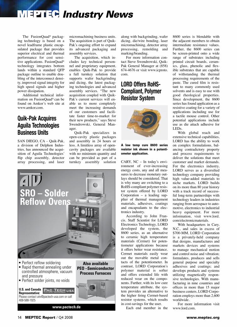
LORD Offers RoHS-Compliant, Polymer Resistor System
A low temp cure 8600 series resistor ink shown in a potenti-ometer application.
CARY, NC – In today’s envi-ronment of ever-increasing energy costs, any and all mea-sures to decrease monetary out-lays should be considered. That is why many are switching to a RoHS-compliant polymer resis-tor system offered by LORD Corporation – a leading sup-plier of thermal management materials, adhesives, coatings and encapsulants to the elec-tronics industry. According to John Fran-cis, Staff Scientist for LORD Electronics Technology, LORD developed the system, the 8600 series, as an alternative to ceramic high temperature materials (Cermet) for poten-tiometer applications because it offers better wear resistance. Cermet materials easily wear out the movable metal con-tacts of the potentiometer. In contrast, LORD Corporation’s polymer material is softer and offers extended life with reduced wear on the compo-nents. Further, with its low cure temperature attribute, the sys-tem provides an alternative to the higher firing Cermet-based resistor systems, which results in cost-savings for the user. Each end member in the
8600 series is blendable with the adjacent members to obtain intermediate resistance values. Further, the 8600 series can be screen-printed onto a wide range of substrates including printed circuit boards, ceram-ics, glass, phenolic and flex-ible substrates that are capable of withstanding the thermal processing requirements of the paste. The cured film is resis-tant to many commonly used solvents and is easy to use with good rheological properties. Since development, the 8600 series has found application as a resistive coating for a variety of applications including use for a tactile mouse control. Other potential applications include use as die attach adhesive for LEDs. With global reach and extensive technical capabilities, LORD has the ability to work on complex formulations, bal-ancing contradictory property and process requirements to deliver the solutions that meet customer and market demands. For the electronics industry, LORD serves as a diversified technology company providing high value-added materials to niche markets. LORD builds on its more than 80 year history with a track record of success-ful long-term partnerships with technology leaders in industries ranging from aerospace to auto-motive, electronics to industrial heavy equipment. For more information, visit www.lord.com/electronicmaterials. With headquarters in Cary, N.C., and sales in excess of $700-MM, LORD Corporation is a privately-held company that designs, manufactures and markets devices and systems to manage mechanical motion and control noise and vibration; formulates, produces and sells general purpose and specialty adhesives and coatings; and develops products and systems utilizing magnetically respon-sive technologies. With manu-facturing in nine countries and offices in more than 15 major business centers, LORD Corpo-ration employs more than 2,600 worldwide. For more information visit www.lord.com.
14 MEPTEC Report / Q4 2008 www.meptec.org
MEPTEC Industry News
U.S. and Canada Representative:Please contact [email protected] or call408-588-1925
www.pactech.de
� Perfect reflow soldering� Rapid thermal annealing under
controlled atmosphere, vacuum and pressure
� Perfect solder joints, no voids
Also available PEO –Semiconductor
Process Furnaces
SRO – Solder Reflow Ovens

Rudolph’s New Explorer Macro Defect Inspection System Gains Traction with Low Cost-of-Ownership
TOKYO, JAPAN – Rudolph Technologies, Inc. has an-nounced the shipment of its new Explorer™ Inspection Clus-ter to a major chip manufacturer located in Japan. The Explorer Inspection Cluster meets the I.C. indus-try’s need for an edge and backside inspection system with low cost-of-ownership to solve critical defectivity issues in advanced manufacturing processes. Rudolph pioneered the field of edge and backside inspection, now in its third gen-eration, with over 120 modules in the field. The Explorer’s flexible clus-ter design allows manufacturers to configure frontside, edge and backside inspection capabilities to meet specific process require-ments. The edge (E30) and backside (B30) modules both use image-based inspection to provide a much richer data set than light scattering techniques, thereby enhancing accuracy in the sizing and classifying of defects. The improved sensi-tivity of the E/B permits the detection of defects down to
2 µm and 3 µm, respectively, on patterned wafers. The E30 module also provides metrolo-gy capability for the edge bevel profile and for multi-film edge bead removal and bevel clean processes. When the E30 and B30 modules are paired with
the AXi940™ frontside module, the system can provide the all-surface data to correlate wafer edge and backside inspection results with improved yield. Additional information can be found on the Rudolph web-site at www.rudolphtech.com.
Gartner Says Obama Plan Could Boost U.S. Solar Development STAMFORD, CN – Barack Obama’s election as the next U.S. president could usher in a
www.meptec.org Q4 2008 / MEPTEC Report 15
� Quick-turn and mass-production
� Highly competitive, low-cost bumping technology
� Exceptional quality through high-level expertise
Available Processes� Electroless Ni/Au under-bump metallization � Ni/Au bump for ACF or NCP assembly� Solder paste stencil printing� Solder ball drop for wafer-level CSP� Solder jet for micro-ball placement� BGA and CSP reballing� Wafer backside thinning and wafer dicing
Special Features/Technologies� Over 10 years experience� U.S. Government Certified� 4- to 12-inch wafer capability� Wafer pad metallization: Al and Cu� Solder alloys: eutectic SnPb37, lead-free,
low-alpha, and AuSn� Fluxless and contactless bumping for MEMS
and optoelectronics� Ni/Au interface for wire-bond applications
The leader in low-cost electroless wafer bumping.
Pac Tech GmbHTel: +49 (0)3321/[email protected]
Pac Tech USATel: 408-588-1925, ext. [email protected]
Pac Tech Asia Sdn. Bhd.Tel: +60 (4) 6430 [email protected]
NAGASE & CO., LTD.Tel: [email protected]
Global Low-CostWafer Bumping Services
• Europe – USA – Asia •

new era of solar energy devel-opment in the United States, but economic difficulties may prove a barrier to some of the more expensive renewable ini-tiatives, according to Gartner, Inc. “Demand for solar energy remains dependent on govern-ment subsidies, because it costs more than conventional forms of electric-power generation,” said James Hines, research director at Gartner and lead analyst for solar energy tech-nologies. “However, the new U.S. administration could help encourage investment in solar energy projects if it succeeds in implementing some of its plans, which is more likely
with majorities in both houses of Congress. This increased emphasis on renewable energy and the extension of the 30 percent investment tax credit for solar projects – passed last month – could finally help real-ize the U.S.’s vast potential for solar energy. As a result, the U.S. could overtake Germany as the largest photovoltaic mar-ket within a few years.” Gartner, Inc. is the world’s leading information technology research and advisory compa-ny. Founded in 1979, Gartner is headquartered in Stamford, Connecticut, U.S.A., and has 4,000 associates, including 1,200 research analysts and consultants in 80 countries. For
more information visit www.gartner.com.
Wafer-Level Packaging Stands Outas a Bright Area in Today’s ElectronicsSAN JOSE, CA – Wafer-level packaging is experiencing ex-ceptional growth and stands out as one of the bright growth areas in electronics today, said Dr. Tom Di Stefano, president of Centipede Systems. WLP, which industry ana-lyst TechSearch International pegs at a 14 percent compound annual growth rate, offers lower
cost, a smaller package, higher performance and added func-tionality compared to older methods. “Wafer-level packaging is a paradigm for making packages of many types by fabricating them in parallel on the wafer,” said Dr. Di Stefano, a pioneer in both WLP and chip-scale pack-aging and a founder of Tessera, one of Silicon Valley’s most successful technology compa-nies. “WLP is a parallel process-ing approach to fabrication of a portion or the entire package directly on the wafer,” he noted. “We are not wire bonding pack-ages or making individual leads. In WLP, we’re fabricating leads
SAN JOSE, CA – North America-based manufacturers of semiconductor equip-ment posted $805 million in orders in November 2008 (three-month average basis) and a book-to-bill ratio of 1.00 according to the November 2008 Book-to-Bill Report published by SEMI. A book-to-bill of 1.00 means that $100 worth of orders were received for every $100 of product billed for the month. The three-month average of worldwide bookings in November 2008 was $805.4 million. The bookings figure is about four percent less than the final October 2008 level of $839.7 million, and about 29 per-cent less than the $1.13 billion in orders posted in November 2007. The three-month average of worldwide billings in November 2008 was $807.3 million. The billings figure is about seven percent less than the final October 2008 level of $871.4 million, and about 42 per-cent less than the November 2007 billings level of $1.38 billion. “The book-to-bill ratio reached par-ity as billings have declined sharper than bookings over the past six months,” said Stanley T. Myers, president and CEO of SEMI. “2008 is closing with expected declines on the year, which have been fur-ther exacerbated by the deepening seismic global economic situation over the past quarter.”
The SEMI book-to-bill is a ratio of three-month moving average bookings to three-month moving average shipments.
Shipments and bookings figures are in millions of U.S. dollars. ◆
Bar scale starts at 255 per increment
1400
1500
1600
1700
1800
1900
2000
16 MEPTEC Report / Q4 2008 www.meptec.org
North American Semiconductor Equipment Industry Posts November 2008 Book-To-Bill Ratio of 1.0
Dec Jan Feb Mar Apr May Jun Jul Aug Sep Oct Nov 08
$805.4
12 Months Ending November 20082000
1500
500
0
1000$807.3
MEPTEC Industry News
Book-to-Bill RatioBook-to-Bill Ratio
.81 .83.78.87 .82.92.85 .89
.70
.96.81
1.00
Average Bookingsin Millions of Dollars
Average Shipmentsin Millions of Dollars

on packages 50,000 at a time, driving cost down a learning curve.” In the past, productivity gains in semiconductor fabrica-tion have taken the spotlight away from the package. The reason, said Dr. Di Stefano, is that “packaging has always had a low-technology 19th Century feel to it: bending leads, stamp-ing metal and smashing wires against hot pads to join them. “The promise of wafer-level packaging is to break free of the constraints of conventional packaging with batch process-ing versus one-at-a-time assem-bly.” The technology also holds great promise for memory devices and CPU chips, but growth in those areas has been delayed by several factors. Many chips are too large for WLP fabrication due to the TCE (thermal co-efficient of expan-sion) mismatch between chip and substrate. “WLP has not really penetrated the DRAM (memory) area. When it does,”
Dr. Di Stefano added, “WLP will become a mainstream pro-cess.” Beyond conventional WLP, every company that produces semiconductor memory is look-ing at stacked chips. “This is an area that could have explosive growth for WLP if it fulfills its promise to give us higher den-sity for memory,” he added. WLP techniques are adapt-able to a diverse set of packag-es, and the same paradigm may be employed for any packaging technology, according to Dr. Di Stefano. “That,” he concluded, “is the future of packaging.”
TechSearch Study Shows Flip Chip and Wafer Level Package GrowthThe growth of flip chip and wafer level packaging is a bright spot in the electronics industry. TechSearch International’s new study, 2008 Flip Chip and WLP
Market Trends and Forecasts, projects a compound growth rate of more than 14 percent for flip chip units and 14 percent for WLPs between 2007 and 2012. The drivers for flip chip continue to be performance and form factor. The use of flip chip for a variety of wireless products will contribute to the growth in 2009. An increasing number of suppliers of ASICs, field programmable gate arrays (FPGAs), DSPs, chipsets, graphics, and microproces-sors are expanding their use of flip chip with solder bumps and copper pillars in package (FCIP). Flip chip on board (FCOB) continues to be found in automotive electronics, hard disk drives, and watch modules. Many companies are planning to use micro bumps for future through silicon via products. The growth in wafer level packages (WLPs) is driven by increased demand for thinner, lighter-weight portable prod-ucts, but WLPs are adopted
for both form factor and per-formance reasons. WLPs have typically been used for low pin count (≤50 I/O) small die size applications, including analog devices such as power ampli-fiers and battery management devices, MOSFETs, image sen-sors, controllers, and integrated passives. However, WLPs are now an option for larger die sizes with higher pin counts (≥100 I/O). The TechSearch study details these develop-ments, including the trends in fan-out WLPs, with descrip-tions and photos. TechSearch International, Inc., founded in 1987, is a market research firm special-izing in technology trends in microelectronics packaging and assembly. TechSearch Inter-national professionals have an extensive network of more than 15,000 contacts in North America, Asia, and Europe. For more information, contact TechSearch at 512-372-8887, fax: 512-372-8889, or online at www.techsearchinc.com. ◆
www.meptec.org Q4 2008 / MEPTEC Report 17

A particularly versatile form of wafer bumping is stud bump-ing(1), using either gold or copper wire. The equipment required is an adaptation of
a traditional wire bonder. A ball bond is made at a first contact pad using heat and ultrasonic energy. The wire is extended in a precise direction and a flying lead is created by terminating the wire, for example using electronic flame-off (EFO). This type of stud bump can be used as a buckled pillar connector, enabling electronic assemblies that are put together with screws rather than solder. With appropriate assembly and test-ing techniques, this can lead to waste-free integrated assemblies; no good parts are thrown away due to compound yield prob-lems, otherwise known as “known good die” or KGD problems.
Why Replace Ball Grid Array (BGA) Packaged Devices? BGA has become the dominant packag-ing type for electronic systems, represent-ing 60% of the total packaging revenue in 2008(2). More and more BGA pack-ages employ a method of direct chip attach (DCA) called “flip chip” (3). IBM created the first BGA packages in 1965, using the C4 process. Recently it has created the C4NP process(4), “Controlled Collapse Chip Con-nection New Process”. C4NP was devel-oped to improve yield and reliability while reducing cost. However, BGA and C4NP still have two serious drawbacks. First, an epoxy underfill is normally required for die sizes larger than around 4mm. The underfill binds the chip and the substrate together to make a robust package that can with-stand the differential stresses induced by temperature cycling, as well as withstand increased levels of shock and vibration. This is a big factor in helping your cell phone survive being dropped. However, the epoxy can not be easily removed if a chip fails in an integrated assembly. The failure could be a subtle flaw that was not detected by the component test program, or it could be assembly-induced. Since the underfill step can not be undone, rework is limited or impossible. For an integrated electronic assembly, rework is the process of finding a defective chip and replacing it. Not having
a viable path for rework presents a serious economic disadvantage. It means for exam-ple that stacked die assemblies employing underfill will incur an additional cost due to compound yield issues. It also means that integrated assemblies employing underfill are limited to around 5 or 6 die, because reject costs become too great for more com-plex assemblies. Finally the underfill itself adds both material and process cost. The second big disadvantage with BGA and C4NP is that they both employ solder. The solder may be lead-free, but it still contributes to environmental and reliability problems(5). Solder is reputed to cause more failures in electronic assemblies than any other single cause; the failures range from solder bridging (shorts), to open traces, to corrosion, creep, cracking at brittle inter-metallic interfaces, and tin whiskers.
The Buckled Pillar Solution Figure 1 is a conceptual drawing show-ing the versatility of buckled pillar connec-tors in a new type of integrated assembly. The buckled pillars are formed by a manu-facturing sequence that is described in detail in reference 6, including an animation of the process steps. In Figure 1, buckled pillars having poten-tially five different lengths are required. Because the bonding tool follows a pro-grammed sequence, the different lengths are easily accommodated in an automated fash-ion. Components are aligned and placed, and the entire assembly is compressed using assembly screws provided in each corner. The screws work against spacers to provide exactly the right amount of compression,
enough to buckle the pillars by a few per-cent in length. This means that the bonding wire material is not stressed above its elastic limit; accordingly it acts like a spring. This helps to provide good electrical contact at the receiving cup end, and also provides some design margin to accommodate minor differences in co-planarity of the tips of the buckled pillars. The system assembly can accommo-date stacked components that employ through silicon vias (TSVs), but TSVs are not required in all of the chips. The TSV stacked component in the figure represents a complex component having very high electrical performance, but at a considerable cost. The additional cost is associated with the intricate processing to form the through vias. This will typically represent a good economic alternative only for the highest production volumes. The module or sys-tem-level assembly method depicted in the figure accommodates many heterogeneous chip types. Nearly all chips that are cur-rently in use via other assembly techniques (such as conventionally packaged devices on printed circuit boards (PCBs), can be used in the compact assembly of Figure 1. The conventional packages are eliminated, providing a substantial cost benefit as well as contributing to a more standard electri-cal, thermal, and mechanical environment. Packages of today encompass so many different types and incorporate so many different design rules with respect to signal integrity and thermal issues as examples; they have become a burden with respect to the design goal of a standardized environ-ment.
18 MEPTEC Report / Q4 2008 www.meptec.org
MEPTEC Integrated Assembly Technology
Solder-Free Connectors Using Buckled PillarsPeter Salmon, Vice PresidentSalmon Technology, LLC
Figure 1. Customized buckled pillar connectors support many assembly configurations.

It may also be desirable to create semi-conductor chip versions of discrete compo-nents such as resistors and bypass capaci-tors, integrating many of these on each chip. The pad pitch can be as fine as 50 µm, using 20 µm wire(7,8). Since the ball bond is formed robustly using heat and ultrasonic energy, nearly all pad metals and under-bump metallurgies can be accommodated. Note that none of the connections include solder. This leads to convenient rework scenarios, wherein a module can be disassembled and a defective chip replaced, using only a placement machine having good alignment capabilities and a screw-driver. High power IC chips may be provided in a single-high layer at the top of the mod-ule as shown. Preferably a soft conductive material such as indium foil will be pro-vided at the silicon-copper interface, for the best possible thermal connection. If electri-cal isolation is required at the back side contact of the chip, a thin coating of silicon nitride can be used. The indium foil fills microscopic voids and helps to eliminate air pockets at the interface. The exposed copper surface at the top of the module is available for heat sinking, providing very low thermal impedance between the transistor junctions in the chip and the heat sink material. In Figure 1 the substrates are preferably made of copper, and fabricated in a large panel size such as 12 x 18 inches. The use of copper provides good heat distribution and enables the use of a water coolant between module layers. Since the power density in such an assembly is much higher than in a regular PCB assembly, good heat distribution and extraction become manda-tory. The interconnection layers shown in yellow are preferably fabricated using direct laser imaging, and this combination of cop-per cores and laser imaging has recently become available. The build-up layers of the interconnection circuits can be fabricated using fine geometries such as 30 µm line and space(9), again supporting the miniatur-ized assembly.
Options for External Connections In Figure 2(a), solder balls have been formed at the bottom face of the module, and the system in package (SIP) presents a BGA interface to the outside world. In Figure 2(b), buckled pillar connections are shown for interfacing between the SIP and a conventional PCB. Figure 2(c) shows that a flex circuit equipped with buckled pillar connectors may be used for external sig-nals.
A New Cost Tradeoff Good cost figures are not yet available for miniaturized 3D assemblies as shown in Figure 1. The build-up technology on copper is substantially more expensive than regular PCB technology employing epoxy-glass laminates. However, a system-level cost
analysis will take into account the following factors: (i) conventional packages for each IC chip are eliminated; (ii) the availability of effective rework strategies may lower the cost of yielded assemblies; (iii) the result-ing assembly will be more compact and more power efficient leading to savings in space and energy consumption. To illustrate this last point, energy consumption in data centers is currently estimated at 20% of operating costs, and power equipment plus cooling equipment add an additional 24% (10). In addition, once the technology has been shaken down, superior reliability may result from eliminating solder, leading to reduced cost from failures in the field.
Where Will This Technology Be Used? 3D assemblies enabled by buckled pillar connectors are a natural fit with high-pow-ered systems such as servers and routers. For blade servers, it is estimated that the new 3D assemblies can reduce space requirements by as much as 50X and weight requirements by as much as 20X. Accordingly, they may become an attractive option for aerospace applications.
Remaining Challenges Although stud bumping machines exist with the necessary adaptations for making buckled pillar connectors, they are not yet produced by mainstream suppliers and are not yet commercially available. Although lapping and chemical mechanical polish-ing (CMP) machines and processes exist for planarizing the tips of the pillars, spe-cific processes are still under development. Mechanical modeling is required to confirm the elastic behavior of copper and gold pil-lars, for specific implementations of wire diameter, pillar length, and compression factor. In the absence of a supporting medi-um such as wax, the buckled pillars must adequately support the embedded chips. Although good shock performance may be achievable with the flexible pillars, this must be confirmed by modeling and experiment. If the technology is combined with water cooling, the primary issue relates to water seals between copper elements. Hydropho-bic wax may be used to keep water away from electronic components, but this must be tested and limits the maximum operat-
ing temperature to around 90°C. To take advantage of the proposed more-standard-ized design environment (excluding chip packages), new design software must be developed and existing software must be integrated into convenient tools. However, the new software may enjoy a much larger market due to wide applicability of the stan-dardized environment.
Conclusion Although much work remains to vali-date and test the proposed 3D structures, the potential benefits are substantial. Building on the versatility of stud bumping machines, the overall technique is versatile and can be adapted to many different substrates and chip stack configurations. Compaction factors as high as 50X may be achievable while providing adequate heat removal, effective re-workability, and high reliabil-ity. Almost all IC chips that are in use today can be utilized without modification. Although no through silicon vias (TSVs) are required, TSV stacks can be accommodated. Using copper substrates, water cooling may become a practical option. ◆
Credit: This article will appear in the January/February 2009 issue of Advanced Packaging Magazine.
References1. Laurie S. Roth and Vice McTaggart, Flip Chip Enabling Technology. http://ap.pennnet.com/Arti- cles/Article_Display.cfm?Section=Articles&Subsec- tion=Display&Article_ID=2209432. Electronic Trends Publication, Inc. The Worldwide IC Packaging Market, 2008 Edition.3. George A. Riley, Introduction to Flip Chip: What, Why, How. http://www.flipchips.com/tutorial01.html4. George A. Riley, C4NP Preliminary Test Data. http://www.flipchips.com/tutorial63.html5. John H. Lau and Yi-Hsin Pao, Solder Joint Reli- ability of BGA, CSP, Flip Chip, and Fine Pitch SMT Assemblies, McGraw-Hill, 1 edition, 1996.6. Peter Salmon, Solder-free Connectors Using Buckled Pillars. http://ap.pennnet.com/display_arti- cle/339446/36/ARTCL/none/none/1/Solder-free- Connectors-Using-Buckled-Pillars/7. Palomar Technologies. http://palomartechnologies. com/ProductsSolutions/Model8000BallStudBumper. aspx8. Kulicke & Soffa. http://www.kns.com/KNS07/Tem- plates/showpage.asp?DBID=1&LNGID=1&TMID= 87&FID=514&PID=14059. Sierra Circuits. http://www.protoexpress.com/con- tent/capability.jsp10. http://www.apcmedia.com/salestools/CMRP- 5T9PQG_R3_EN.pdf
www.meptec.org Q4 2008 / MEPTEC Report 19
Figure 2. BGA, buckled pillar, and flex circuit options for external connections.

A s flip chip packaging technol-ogy gains greater acceptance and volume usage continues growing, more packages are being over molded rather then
the older method of using glob top. Hes-tia Technologies, Inc. patented molded underfill process “MUF”® allows you to over mold and underfill at the same time with the same mold compound. This tech-nology offers reduced assembly process steps, reduced floor space, requires no special additional equipment and most importantly reduces assembly cost. While much has been written about some of the different ways to underfill packages i.e.: liquid and vacuum assisted, little to nothing has been written about the most cost effective process. “MUF”®
technology uses a venting process, which requires adding a hole or holes in the sub-strate under the die. Transfer molding technology, has been used for decades in volume production of IC packages world wide with a very successful history. The epoxy molding compound (EMC) is a very well under-stood chemistry which has been highly optimized over the years for the packaging industry. The standard transfer molding process used for substrate packages is a highly efficient, cost effective method for mold-ing packages of all types. There is also
a large amount of existing infrastructure world wide already in place in equip-ment, tooling and knowledge. However, using liquid underfill adds additional cost for material, equipment, floor space and added cycle time. The Vacuum assisted process adds additional cost to modify existing equipment or to add new expen-sive required equipment. This technology also has the capability of leaving the back of the die exposed for added thermal dissipation. (See above) The “MUF”® Molded Underfill process offers many advantages over the other pro-cess presently available: • Underfill and over molding using the same mold compound• No secondary processing required like liquid underfill• No additional expensive equipment required like liquid and vacuum assisted
• Reduced assembly process steps• Reduced cycle time • Increased productivity• Reduced floor space• No secondary curing required• Uses existing molds and molding equipment• Lower CTE values 20-30ppm/ degree C
Lower Cost The Hestia patented “MUF”® process requires a small vent hole or holes in the substrate directly under the die. More then one hole may be required depending on die size. The “MUF”® technology adds no additional cost to the substrate design or substrate manufacturing cost and requires no additional cost for unneeded equip-ment. For more information email Hestia at [email protected]. ◆
20 MEPTEC Report / Q4 2008 www.meptec.org
MEPTEC Molding Technology
Molded Underfill “MUF”® Technologyfor Flip Chip PackagingHal Shoemaker and Pat Weber Hestia Technologies, Inc.
Editorial (continued from page 30)
at less than 0.5mm in diameter and 2mm long, the Ibetics analyzer will contain sen-sor, measuring electronics, and transmitter necessary to send tear glucose values to your cell phone. Not only will the Ibetics device obviate the need to remember to measure one’s glucose, but will send an alert to the uncontrolled patient. Other promising technologies include analytical systems placed in each pill you swal-low (adding only a penny to the cost) to determine physiologically if you actually derived any health benefit from the pill you just swallowed. The pill would couple electronically through the liquid in your body to an externally worn device that would gather, reduce, and display the data.
The increasing percentage of elderly has been called a “tsumami” of medical needs that will bankrupt our already finan-cially strapped medical system. Chronic disease, which consumes over 80% of the health care dollar, is most prevalent in those over 65 years of age. The “hospital without walls” is a term that has been coined to describe the growing trend of using the home as the most likely afford-able location in which to deliver medical care. Telemedicine and remote diagnostic devices will bring medical care to those who need it most, and are most likely not able to afford conventional hospital based medicine. We have developed a suite of passive sensing technologies that measure quality of sleep using a modified mattress pad, human falls using a vibration monitor on the floor, and other physiologic rel-
evant parameters. Microelectronic devices allow the sensor signals to be quantified at the level of the device, and allow rel-evant data to be passed up to the computer server which manages the system. In case controlled studies, we demonstrated a 75% savings in the cost of caring for elders by deploying the passive sensing system with interpretive software. Electronic design and packaging is the fundamental basis for this technological revolution in health care. Medical auto-mation is stimulating the creating of new ideas and inventions for the benefit of the health of future generations. ◆
Cited literature:1. Felder RA, Alwan MA, Zhang M, (Eds.). Systems Engineering Approach to Medical Automation, Artech House, Inc., Norwood, MA, USA, 2008. ISBN-13; 978-1-59693-164-0
MOLD MOLDED UNDERFILLMOLD MOLDED UNDERFILLFLIP CHIP
MOLD MOLDED UNDERFILL
SOLDER BALLVENT HOLELAMINATE SUBSTRATE

“We found new SMTequipment at APEX
that’s given us better machine optimization,
reduced cycle times and fewer defects.”
Chuck Needham, Director, Sales & Product Management,
Phoenix International Corp.
Mandalay Bay Resort & Convention CenterLas Vegas, Nevada USA
Conference & ExhibitionMarch 31–April 2, 2009
MeetingsMarch 29–April 2, 2009
PCB and Electronics Manufacturing Trade ShowSolve your manufacturing challenges, visit hundreds of exhibitors and meet thousands of peers and industry experts in board design and manufacture, electronics assembly, and test.
Benefit from the industry’s premier technical conference, more than 60 full- and half-day courses and IPC standards development meetings. Focus on advanced technologies, environmental regulations, materials and SMT processes. Pre-register for free exhibit hall admission and take advantage of free keynotes, posters and forums.
www.IPCAPEXEXPO.org
Certified by:

22 MEPTEC Report / Q4 2008 www.meptec.org
MEPTEC Solder Sphere Alloy Development
In the early 2000s when semi-conductor package assemblers began making the switch to leadfree solder sphere alloys, the most common choices were
alloys like SAC305 or SAC405. These “high-Ag” alloys were adopted as the standard, and experience was gained using them over the following years. It became well understood that high-Ag alloys demonstrated acceptable ther-mal cycling reliability, in many cases even better than Sn63/Pb37. How-ever, as the handheld device market continued to grow, it became evident that high-Ag alloys were deficient to Sn63/Pb37 for dropshock perfor-mance. Since drop-shock resistance is a critical attribute for components going into handheld devices, alternate materials had to be explored. In the past three years, alloys like SAC105 and SAC125 have been adopted for use in such parts. These “low-Ag” alloys exhibit superior drop-shock or impact resistance com-pared to their high-Ag predecessors. However, temperature cycling perfor-mance was sacrificed. As a result, most semiconduc-tor package assemblers are forced to utilize multiple lead-free alloys depending on desired performance attributes, package requirements, and end customer specifications. Today, most component assemblers are using at least two (and in many cases even more) lead-free solder sphere alloys to meet various package requirements. Cookson Electronics has engaged in a significant program to develop a solder sphere alloy which provides the drop-shock performance of SAC105 or better, combined with the tempera-ture cycling performance of SAC305 or better. Cookson Electronics’ SACX® alloy demonstrates extremely encouraging results. The SACX® alloy is comprised
of 0.3% Ag / 0.7% Cu / plus “X”. Test data shows that this alloy offers the targeted combination of excellent drop shock performance AND temperature cycling reliability. The following key attributes contribute to this alloy’s exceptional reliability performance:
• Low Ag reduces the probability of Ag3Sn intermetallic precipita- tion in the bulk solder which results in improved drop shock resistance.
• “X” addition increases solder spread and wetting which im- proves the overall integrity of the solder joint.
• “X” addition controls the interfa- cial IMC thickness which im- proves drop-shock resistance.
• “X” addition also modifies the bulk grain structure, resulting in: - Increased solder strength - Improved creep resistance - Improved temperature cycling reliability
Cookson Electronics utilizes the JEDEC test protocol for measuring drop shock resistance. Figure 1 shows the relative drop-shock performance of SAC305 vs. SAC105 vs. SACX®.
For this evaluation Cookson Elec-tronics is testing temperature cycling under the following conditions: -55°C to 125°C with a 10 minute dwell at each stage. Figure 2 shows the relative performance of the alloys under test.
The other low-Ag alloys all failed around the same time at approximate-ly 4,000 – 4,300 cycles. The SACX® and SAC305 alloys have yet to fail, having already survived >6,500 cycles to date. This already represents over 60% improvement compared to the other low-Ag alloys and still going strong. This excellent combination of drop shock and temperature cycling reli-ability could allow component assem-blers to converge to a single lead-free alloy which meets all demanding reli-ability requirements. In addition to solder spheres, Cook-son Electronics offers other SACX® family solder products, such as solder paste, cored wire and bar solder. To learn more, please contact your local Cookson Electronics Semiconductor Products representative or visit www.cooksonsemi.com. ◆
Drop Shock Performance AND TemperatureCycling Reliability from a Single Lead-Free Alloy?Robert Healey and Ranjit Pandher Cookson Electronics Semiconductor Products
Figure 1. Drop Shock test results using 0.30mm (12mil) spheres at 0.5mm pitch attached to CABGA84 substrate with NiAu pad finish.
Figure 2. Temperature cycling test results. Test conditions are -55°C to +125°C with a 10 minute dwell at each stage.

Do you experience high missing-ball rates during the ball attach process? Are you constantly making trade-off decisionsbetween high drop-shock alloy reliability and temperature cycling performance. Is flip-chip die misalignment or underfilldelamination reducing your package yield?
Cookson Electronics Semiconductor Products line of solder productswill deliver consistently reliable package results while helping youcontrol process costs and increase yield. Our commitment to highlevel R&D drives our world class formulation capabilities. We offer:• ALPHA® Flux for BGA/CSP/wafer level ball attach, flip chip attach
and wafer bumping• ALPHA® Solder Spheres for area array packages, wafer-level
packages, flip chip wafer bumping and substrate bumping• ALPHA® Solder Paste for component attachment and wafer
bumpingFor more information about Cookson Electronics semiconductorsolder products, and our epoxy mold compounds and electronic polymer lines, go to www.cooksonsemi.com. or contact your Cookson Electronics Semiconductor Products representative.
Worldwide Headquarters • 3950 Johns Creek Court, Suite 300 • Suwanee, GA, USA • +1-888-263-0443Asia-Pacific Headquarters • 12 Joo Koon Road • Singapore-628975 • +65-6861-0244© 2007 Cookson Electronics
alpha
®What demanding solderrelated packagingchallenges do youface every day?
What demanding solderrelated packagingchallenges do youface every day?
What demanding solderrelated packagingchallenges do youface every day?
What demanding solderrelated packagingchallenges do youface every day?
What demanding solderrelated packagingchallenges do youface every day?
cookson_cesp_ad.qxp 10/30/07 7:32 AM Page 1

F or nearly two decades, flip chip technology has been widely used and accepted for several main-stream and high-end applications including flat panel displays and
semiconductor modules in the form of chip (die) on glass (COG) and chip (die) on flex (COF). To facilitate the interconnect within these applications, anisotropic conductive films (ACFs) have generally been the pre-ferred material for several reasons: ACF’s offer excellent low contact resistance and compatibility with noble metallization, they have outstanding adhesion to glass and offer highly reliable interconnection on fine reso-lution lines. But, the higher materials costs of ACFs combined with their multiple-step processing requirements and higher cure temperatures make them a less than ideal solution for some of today’s lower-cost consumer applications. As the benefits of flip chip technology have been realized for high-end applica-tions, this process is also finding favor among manufacturers in the consumer products realm. In particular, these devices have proliferated in applications such as RFID and mobile phones. But lower-cost consumer electronic products pose different challenges than their high-end counterparts and, therefore, require alternative and more cost-effective materials to facilitate high yield, low cost production. Particularly in the case of RFID devices, which are found in everything from pet ID tags to depart-ment store inventory oversight, controlling the production cost and enabling extremely high throughput rates is essential to wide-spread use of the technology. For RFID assembly and many other low-cost applica-tions, the interconnect adhesive must be less costly than alternative materials, deliv-er faster throughput, be compatible with lower processing temperatures and provide very good compatibility with non-noble metals such as etched copper (Cu) and etched aluminum (Al). Because anisotropic conductive films don’t deliver on these
requirements, anisotropic conductive pastes have emerged as the most cost-effective interconnect material for RFID assembly. But, as RFID inlay manufacturers continue to reduce the cost of the tags by using lower cost substrates such as PET (Polyethylene terphthalate or also know as Polyester) and antennae metallizations like etched aluminum, die cut aluminum and etched copper, traditional anisotropic conductive paste (ACP) materials aren’t offering the
robust performance these devices demand. The most common issue with conventional ACPs when used with non-noble RFID antenna metallizations is that they are prone to galvanic corrosion when subjected to high humidity and high temperature envi-ronments. Because of this, the materials specialists at Henkel set out to develop a newer gen-eration ACP that delivered the known ben-efits of existing ACP formulations – snap cure capability at low temperature, strong adhesion to etched aluminum and etched copper, long work life at ambient tempera-ture and a low interconnect contact electric resistance – and extend them to include corrosion resistance. Building on an exist-ing and well-proven Henkel ACP material, the company’s chemical scientists applied Design of Experiment (DOE) methodology to modify the formula, making it corrosion resistant in humid, higher temperature envi-ronments and its rheology more suitable to
jet dispensing. Through filler modification and mixture optimization, Henkel’s techni-cal team was able to engineer a robust ACP formulation that addresses all of the needs of modern, low-cost RFID assembly. The new material, called Acheson® CE-3126, not only meets all of the processabil-ity requirements of good adhesion strength, snap cure capability and a long work life, but also has a much improved reliability performance on non-noble metal substrates as compared to older-generation versions. Damp heat and thermal shock tests were carried out on the new ACP on three types of non-noble metal antennae: etched alu-minum, etched copper and vapor deposited copper. In all three cases, Acheson CE-3126’s contact joint resistance remained less than 1 ohm after aging in both 85°C at 85% relative humidity (RH) up to 168 hours and after 200 thermal shock cycles. The material also offers exceptional pro-cess versatility, as it can be screen printed, dispensed or jetted to address a variety of manufacturing preferences. RFIDs and other low-cost electronics devices are part of our everyday life – some-times even unbeknownst to us. The technol-ogy that affords our common conveniences must also address consumer-driven cost pressures and RFID specialists, who have turned to lower-cost substrate and antenna metallizations and now require complimen-tary materials to enable robust assembly, performance and reliability. Henkel has answered the call with Acheson CE-3126. Now, manufacturers of RFID and other low-cost electronics products can have the best of both worlds, with an ACP from Henkel that addresses financial constraints while also delivering robust performance and reliability. For more information on Acheson CE-3126 or any of Henkel’s advanced electron-ics materials, call the company’s headquar-ters at 949-789-2500. ◆
24 MEPTEC Report / Q4 2008 www.meptec.org
New Corrosion-Resistant Conductive Adhesive for Consumer ApplicationsDelivers Cost-efficient Alternative to Current Technologies
Bo Xia, Jayesh Shah and Wanda O’HaraHenkel Corporation
December 2008


SMT, COB, COF, IC ASSEMBLYSAME DAY, 1 - 5 DAYS TURN
— SMT ASSEMBLY,Lead-Free, 0201, uBGA, CSP
— COB, COF, IC ASSEMBLY, Cleanroom ISO 7 (Class 10,000), Aluminum and Gold wire— NPI - PROTOTYPE, 8, 24 to 72 hours turn— Low to Medium Volume PRODUCTION, MRP, IPC-A-610 Class 2 and 3, MIL-STD-883
Your NPI Manufacturing Solution!
Phone (408) 227-8885Email: [email protected]
AmTECH is a leadingSilicon Valley providerfor SMT, COB, COF andIC Assembly.
Gold ball, aluminumand gold wedge wirebonding, AutomatedOptical Inspection(AOI) and XRAY.
www.amtechmicro.com
26 MEPTEC Report / Q4 2008 www.meptec.org
MEPTEC Network
“Time Critical” Semiconductor Substrates
BGA, CSP, Flip Chip, High Frequency, High Speed and Thermally Enhanced
Rigid and Flex Packages
ACL is the onlyNorth American companyfocusing exclusively on thefabrication of “Quick Turn”semiconductor packages.
Phone: 408.327.0200 Email: [email protected]
www.aclusa.com
AdvancedComponentLabs, Inc.
COMPLEX FLIP-CHIP ASSEMBLY WITH SAME DAY TURN
• Over 3200 bump/ball IO’s• Flexible Process Flows• Wide Material Selection• Gold Stud Bumping• Prototypes: as quick as 8 hours! • Production: 1000’s of units per week
CORWIL has developed into the premier U.S.-based packaging subcontractor with world-class wafer thinning, dicing, pick-and-place and visual inspection, plus state-of-the-art IC assembly in BGA, ceramic, plastic, QFN, COB and MCM packages. In addition to flip-chip capability, CORWIL has outstanding wirebonding expertise for ultra-fine pitch applications in gold and aluminum wire.
Since 1990 CORWIL has built its reputation providing customers with:
Excellent Quality and Superior ServicePhone 408-321-6404 • Fax 408-321-6407
www.corwil.com
HANA Microelectronics
Servicing the Semiconductor Industry for over 25 years with manufacturing locations in Thailand and China.• Specializing in Low Pin count Plastic Packages• Ceramic and Laminate LGA’s• Standard and Custom QFN’s• Custom Package Development for Sensor Applications.• Full service Semiconductor processing including; Back Grinding, Wafer Saw, Packaging, Test and Drop Shipment coordination• Lead Free, Green and RoHS compliant Packages available• QS9000, TS16949, and ISO14001 Certified
For more information visit our website or call Bruce Stromstad at 408-467-0911.
www.Hanagroup.com
NOW! 300mm WAFER DICING
CORWIL is the leader in wafer backgrinding, wafer dicing and visual inspection to commercial, military and medical specs. CORWIL’s newest addition in dicing equipment is a fully automatic, latest state-of-the-art 12 inch dicing saw that strengthens CORWIL’s technical leadership for chip-free and fast turn-around dicing. CORWIL dices Si, GaAs, Sapphire, SiGe, laminates and many other materials and CORWIL is unsur-passed in IC assembly in ceramic, BGA, flip-chip, and MLF/QFN type packages.• High Volume – millions of dice per month.• Automatic High-Speed Pick & Place• Automatic Vision Inspection Systems • Low K, MEMS and Optical/Imaging wafers processed• Experts in Multi-die Type Wafer dicing • Highest Quality and Best Service in the Industry
Since 1990 CORWIL has built its reputation providing customers with:
Excellent Quality and Superior ServicePhone 408-321-6404 • Fax 408-321-6407
www.corwil.com

MEPTEC Network
www.meptec.org Q4 2008 / MEPTEC Report 27
Enabling you to take new products to market faster than by any other route
• IC Assembly Services: molded plastic & ceramic • Custom Package Development & Assembly• Quick Turns through pre-Asia Volume Production
Molded plastic, ceramic and materials-centric custom package develop-ment & assembly services including SiPs, MEMS, MOEMS, MCM and LGAs. JEDEC standard and cus-tom QFN/ DFNs available. PROMEX is a recognized leader in stacked die, thin
molded, 2D, 3D, SMT and RoHS compliant packag-ing. Same day quick turns, development prototyp-ing, “fast track” new product introductions and beta manufacturing through pre-Asia volume production.
Silicon Valley’s Packaging FoundryTel. 408.496.0222
www.promex-ind.com
Quick Turn •DaisyChain •TestDie •Mechanicals •BGA •QFP •FlipChip
[email protected](800) 776-9888
Best Dummiesin Town
www.TopLine.tv
DesignCon 2009Conference February 2–5 2009 / Exhibition February 3–4 2009
Santa Clara Convention Center • Santa Clara, California, USA
Designed by engineers, for engineers, the conference and exhibition brings together the brightest minds in electronic design.Visit designcon.com/2009
Are you a Chiphead… What Kind of Chiphead are You?DesignCon is a definitive event for electronic design experts spanning chip, package, board, and system domains, addressing common issues in signal integrity, power management, intercon-nection, and design verification. Discover your own technology niche through DesignCon’s rich program of educational sessions and technology exhibits covering analog, verification, IP, PCB, PDN, and signal integrity... all designed to bring out the Chiphead in you.
Keynote SpeakersMark Gogolewski, Chief Technology Officer, Denali SoftwareWalden Rhines, Chairman and CEO, Mentor GraphicsPaolo Gargini, Director, Technology Strategy, Intel
Are you an IP Chiphead?… Announcing the IP SummitThe IEC is pleased to announce the IP Summit at DesignCon, featuring dedicated educational sessions and technology dem-onstrations on semiconductor IP and system-on-chip design. As the industry increasingly relies on semiconductor IP to deliver complex designs in a timely manner, the IP Summit will raise the visibility of this subject area at DesignCon.
Exhibits PLUS — Your Chiphead Express PassAn Exhibits PLUS Chiphead Express registration allows for full access to the show floor, PLUS a multitude of complimentary edu-cational sessions including the following:
• Keynotes• Technical panels• Exhibition• Networking receptions• TecPreview presentations
LEARN the latest in electronic design from more than 130 companies demonstrating their latest products and services.
IMPLEMENT new solution techniques to your most chal-lenging design problems by meeting the vendors that offer practical solutions.
NETWORK with your fellow Chipheads walking the show floor to gain knowledge, exchange experiences, and develop relationships.


27 28
FE
BR
UA
RY
2
00
91
28 29
15 16 17 18 19 2120
22 23 24 25 26 2827
1 2 3 4 5 76
8 9 10 11 12 1413
15 16 17 18 19 2120
22 23 24 25 26
1 32
6 7 8
SUNDAY MONDAY TUESDAY WEDNESDAY THURSDAY FRIDAY SATURDAY
3130
JA
NU
AR
Y
20
09
27
1
18 19 20 21 22 2423
1 2 3 4 5 76
8 9 10 11 12 1413
4 5
25 26
11 12 13 14 15 1716
109
3130
www.meptec.org Q4 2008 / MEPTEC Report 29
29MA
RC
H
20
09
SOUTHWESTMEPTEC LUNCHEON
Dobson Ranch InnMesa, AZ
SMTA PAN PACIFIC MICROELECTRONICS SYMPOSIUM & EXPOFebruary 10 - 12, Hapuna Beach Prince Hotel, Hawaii
SUNNYVALE MEPTEC LUNCHEON
Lookout RestaurantSunnyvale, CA
SPRING BEGINS
MEPTECSEMICONDUCTOR
PACKAGING SYMPOSIUM San Jose, CA
MARTIN LUTHER KING JR. DAY
PRESIDENT’S DAY
ST. PATRICK’S DAY
SOUTHWESTMEPTEC LUNCHEON
Dobson Ranch InnMesa, AZ
SUNNYVALE MEPTEC LUNCHEON
Lookout RestaurantSunnyvale, CA
WASHINGTON’SBIRTHDAY
LINCOLN’S BIRTHDAY
VALENTINE’S DAY
NEW YEAR’S DAY
DESIGNCON 2009February 2 - 5
Santa Clara Convention Center, Santa Clara, California
SEMICO SUMMIT 2009March 8 - 10, Camelback Inn, Scottsdale, AZ
DAYLIGHT SAVING TIME BEGINS

30 MEPTEC Report / Q4 2008 www.meptec.org
MEPTEC Editorial
A utomation has enabled almost every industry in the USA to produce higher quality goods at lower costs and at higher production rates. However,
healthcare has lagged behind its industrial counterparts in the adoption of automation and cost saving technologies. The delay in innovation has resulted in healthcare becoming a 2 trillion dollar industry in the United States (one of the most expensive healthcare system in the world), which does not necessarily result in improved health nor longer life expectancy when compared to other countries. Healthcare workers are required to perform flawlessly complex procedures and deal with com-plex data well beyond what would be con-sidered safe in any other industry, with the outcomes being literally a matter of life and death. While major reform is needed from the top down in the healthcare sys-tem, there is a growing awareness that a bottom up approach using automation may be more affordable and rapidly deployed. We have coined the term “Medical Auto-mation” to define the integrated use of automation, electronics, robotics, infor-matics, process management, and other techniques and technologies to streamline the delivery of healthcare. Medical auto-mation is not a new concept. However the novelty in medical automation is how to apply technology enabled business orga-nizational and process management prin-ciples to medicine that will enable the industry to deliver high quality goods at a low price.(1) Many of the advancements in medicine are the result of miniaturization and pack-aging of electronic circuits. Using these devices, there are countless opportunities in all aspects of medicine to improve pro-cesses and weed out waste. For example, pharmaceutical dispensing has been shown to have error rates as high as 20% in hos-pitals and up to 10% in neighborhood pharmacies. Automated pharmacies are now capable of maintaining hundreds of pharmaceuticals (the formulary) in auto-mated dispensing systems. These systems can quickly and accurately fill an elec-tronically ordered prescription with error rates that are less than one per million events. Furthermore, software algorithms
prevent patients from receiving various prescription medicines that might have negative health consequences when used at the same time. Another exciting medical subspecial-ty experiencing a technological revolu-tion is surgical robotics. Surgical robots are essentially remote manipulators that extend the reach of a surgeon through small incisions in the skin capable of allowing laparoscopic surgery to perform a cardiac bypass, removal a prostate or gall bladder. Patients undergoing robotic surgery have better outcomes and more rapid return to their normal activities since wide area incisions are not necessary. Surgical tools include a camera that pro-vides the surgeon with a wide angle and clear view of the surgical field, a retractor for manipulating tissue, and a cutting tool (usually through cauterization). The micro-scale equivalent to surgi-cal robotics are ingestible robots that can image intestinal tumors or sources of inap-propriate blood in the intestine and actual-ly take a biopsy so that a small piece of the tumor may be retrieved for examination by a pathologist. Behind all this wizardry in health care transformation, is the need for more power efficient, space efficient, and cost efficient electronic circuits. Viewing the insides of the intestines or stomach using inserted flexible scopes is being sup-planted by pill-sized cameras that transmit real-time images through your body to a receiver worn on the belt. Shrinking a camera to pill-sized dimensions takes advantage of technological advancements in camera, support electronics, and pack-aging design so that it can take full color videos of the stomach, large intestine, and small intestine as it passed through the intestinal track. Despite a current draw of a time averaged 20 milliwatts the pill cam is still in need of better battery technol-ogy or more efficient circuits in order to provide a full intestinal scan. Many of these automated micro-scale technologies will require the development of dedicated high density circuits in order to be placed minimally invasively in body cavities and orifices, or inserted invasively into the body. The PillCam™ employs a number of custom integrated circuits for analog to digital conversion, memory array, logic,
and signal transmission. The leading medical discipline to embrace automation was the clinical laboratory, with the first robots being employed in the late 1980s in Japan under Dr. Masahide Sasaki (Kochi Medical School). Clinical laboratories borrowed heavily from industry since they adopted the same automation principles used in bottling beverages, and filling liquid based prescription medicines. Conveyor belts are now transporting blood tubes to pre-ana-lytical stations where they are automatical-ly processed, preventing the potential of laboratory acquired infections by laborato-ry technologists. Clinical analyzers, which take samples directly out of the open tubes on the conveyor belts as they pass by, have taken advantage of miniature sensor and electronic circuits in order to provide high precision and unprecedented throughput in laboratory testing. Not only has laboratory automation reduced the potential for expo-sure to AIDs and other infectious diseases, but also reduced the errors that result from the tedium of analyzing thousands of tubes of blood a day. The micro-scale equivalent to the clini-cal laboratory is the point-of-care analyz-er. The current market for glucose (which is important in diabetes management) is approximately 5 billion dollars per year. Point-of-care glucose analyzers are cur-rently available that are designed to plug into the information port of the cell phone. After placing a drop of blood on a test strip, the patient inserts it into the min-iature analyzer, the data is automatically sent to a remote site that provides remote storage and interpretation. Individuals who have their glucose in unhealthy concentra-tions can receive a cell phone text message prompting them to either inject insulin, or eat some glucose containing food. Patients demand portable devices that require the latest generation in electronic miniaturiza-tion and ability to withstand the abuses of daily use. Minimally invasive systems will take electronic miniaturization to new levels. Imagine a glucose analyzer placed discreetly in the tiny hole at the end of your eyelid (the lachrymal canaliculus) where tears are aspirated into your nose
(continued on page 20)
Medical Automation: Fueling the Demand and Increasing the Complexity of Electronics Packaging
Robin A. Felder, Ph.D., Professor of Pathology, Associate Director Clinical ChemistryThe University of Virginia, Charlottesville, VirginiaChair, Medical Automation.org

Preserve your
environment through
high performance.
Day after day
w e s u p p o r t y o u r i n n o v a t i o n
PageWafer®
Powered performance reliabilityand extended lifetime for hermeticallysealed MEMS packages
� The innovative getter thin film
for wafer-level packaged MEMS
� Improved performance reliability
for accelerometers, gyroscopes,
RF filters, IR sensors
� The easiest integration of getter thin
film at wafer-level
� MEMS vacuum long-term stability
MEPTEC ADV MEMS 2008.qxp 14/02/2008 12.04 Pagina 1

Perfection Products Inc.1320 S. Indianapolis Ave. • Lebanon, IN 46052Phone: (765) 482-7786 • Fax: (765) 482-7792
Check out our Website: www.perfection-products.comEmail: [email protected]
Grip Ring Shippers
I. C. Trays - Multi-Channel
Lead Frame Magazines - F.O.L./E.O.L.
Film Frame Magazines
Film Frames Film Frame Shippers
TO Tapes & Magazines
Magazines and Carriers for Process Handling Solutions
Accept Nothing Less.
Substrate Carrier Magazines
Stack Magazines - E.O.L.
Wafer Carriers
Process Carriers (Boats)
Boat Magazines
Grip Rings
Miscellaneous Magazines
I. C. Tubes and Rails
Grip Ring Magazines