a quantum chemical view of molecular and nano - diva portal
TRANSCRIPT

A Quantum Chemical View of Molecular and
Nano-Electronics
Jun Jiang
Theoretical Chemistry
Royal Institute of Technology
Stockholm 2007

c© Jun Jiang, 2007
ISBN 978-91-7178-618-0
Printed by Universitetsservice US AB,
Stockholm, Sweden, 2007

3
Abstract
This dissertation presents a generalized quantum chemical approach for electron transport
in molecular electronic devices based on Green’s function scattering theory. It allows to
describe both elastic and inelastic electron transport processes at first principles levels of
theory, and to treat devices with metal electrodes either chemically or physically bonded to
the molecules on equal footing. Special attention has been paid to understand the molec-
ular length dependence of current-voltage characteristics of molecular junctions. Effects of
external electric fields have been taken into account non-perturbatively, allowing to treat
electrochemical gate-controlled single molecular field effect transistors for the first time.
Inelastic electron tunneling spectroscopy of molecular junctions has been simulated by in-
cluding electron-vibration couplings. The calculated spectra are often in excellent agreement
with experiment, revealing detailed structure information about the molecule and the bond-
ing between molecule and metal electrodes that are not accessible in the experiment.
An effective central insertion scheme (CIS) has been introduced to study electronic struc-
tures of nanomaterials at first principles levels. It takes advantage of the partial periodicity
of a system and uses the fact that long range interaction in a big system dies out quickly.
CIS method can save significant computational time without loss of accuracy and has been
successfully applied to calculate electronic structures of one- , two- , and three-dimensional
nanomaterials, such as sub-116 nm long conjugated polymers, sub-200nm long single-walled
carbon nanotubes, sub-60 base pairs DNA segments, nanodiamondoids of sub-7.3nm in
diameter and Si-nanoparticles of sub-6.5nm in diameter at the hybrid density functional
theory level. The largest system under investigation consists of 100,000 electrons. The for-
mation of energy bands and quantum confinement effects in these nanostructures have been
revealed. Electron transport properties of polymers, SWCNTs and DNA have also been
calculated.

4
Preface
The work presented in this thesis has been carried out at the Department of Theoretical
Chemistry, Royal Institute of Technology, Stockholm, Sweden.
List of papers included in the thesis
Paper I A generalized quantum chemical approach for elastic and inelastic electron trans-
port in molecular electronic devices, J. Jiang, M. Kula, and Y. Luo, J. Chem. Phys. 124,
034708, 2006.
Paper II An elongation method for first principle simulations of electronic structures and
transportation properties of finite nanostructures, J. Jiang, K. Liu, W. Lu and Y. Luo, J.
Chem. Phys. 124, 214711, 2006.
Paper III An efficient first-principles approach for electronic structures calculations of
nanomaterials, B. Gao, J. Jiang, K. Liu, Z.Y. Wu, W. Lu, and Y. Luo, J. Comput. Chem.,
revision.
Paper IV Length dependence of coherent electron transportation in metal-alkanedithiol-
metal and metal-alkanemonothiol-metal junctions, J. Jiang, W. Lu and Y. Luo, Chem.
Phys. Lett., 400, 336, 2004.
Paper V Electron transport in self-assembled conjugated polymer molecular junctions,
W. Hu, J. Jiang, H. Nakashima, Y. Luo, K. Chen, Z. Shuai, K. Furukawa, W. Lu, Y. Liu,
D. Zhu, and K. Torimitsu, Phys. Rev. Lett. 96, 027801, 2006.
Paper VI Quantum confinement in nano-diamondoids, J. Jiang, L. Sun, B. Gao, Z.Y.
Wu, W. Lu, J.L. Yang, and Yi Luo, Phys. Rev. Lett., submitted.
Paper VII First-principles simulations of inelastic electron tunneling spectroscopy of molec-
ular junctions, J. Jiang, M. Kula, W. Lu and Y. Luo, Nano Lett. 5, 1551, 2005.
Paper VIII Probing molecule-metal bonding in molecular junctions by inelastic electron
tunneling spectroscopy, M. Kula, J. Jiang, and Y. Luo, Nano Lett. 6, 1693, 2006.
Paper IX First-principles study of electrochemical gate-controlled conductance in molec-
ular junctions, W.-Y. Su, J. Jiang, W. Lu and Y. Luo, Nano Lett. 6, 2091, 2006.

5
List of papers that are not included in the thesis
Paper I Electronic structures and transportation properties of sub-60nm long single-
walled carbon nanotubes, J. Jiang, W. Lu, and Y. Luo, Chem. Phys. Lett. 416, 272,
2005.
Paper II Quantum chemical study of coherent electron transport in oligophenylene molec-
ular junctions of different lengths, W.-Y. Su, J. Jiang, and Y. Luo, Chem. Phys. Lett., 412,
406, 2005.
Paper III Effects of hydrogen bonding on the current-voltage characteristics of molecular
devices, M. Kula, J. Jiang, W. Lu, and Y. Luo, J. Chem. Phys., 125, 194703, 2006.

6
Comments on my contribution to the papers included
• I was responsible for calculations and for writing of Papers I and II.
• I was responsible for part of method development and calculations and have partici-
pated in discussions for Paper III.
• I was responsible for calculations and writing of the first draft for Paper IV.
• I was responsible for calculations and part of writing of the manuscript for Paper V.
• I was responsible for calculations and writing of the first draft for Papers VI and VII.
• I was responsible for part of calculations and have participated in discussions for Paper
VIII.
• I was responsible for part of calculations and have participated in discussions for Paper
IX.

7
Acknowledgments
This thesis would have been very difficult to produce without the help of many people,
whom I would like to thank:
Firstly, I would like to express very sincere gratitude to my supervisor Prof. Yi Luo for
introducing me to my research field and for creating a very stimulating and encouraging
working environment with a constant flow of fresh ideas. Many thanks for his great patience
and optimistic attitude. Also, I much appreciate Luo’s help and advice in my ordinary life,
which not only made my life in Sweden joyful but also helped me through some hard time.
I would also like to thank Prof. Hans Agren for giving me the opportunity to study at the
Department of Theoretical Chemistry.
I devote my enormous thanks and gratitude to my supervisor Prof. Wei Lu at the Shanghai
Institute of Technical Physics, who led me to the wonderful scientific world, and acted as
a model of responsible scientist to me. Thanks to my second supervisor Prof. Ning Li for
the guidance and friendship. Thanks to Prof. Wenlan Xu and Prof. Xiaoshuang Chen for
helping me to understand solid physics theory.
I wish to thank Dr. Ying Fu and Yaoquan Tu for explaining to me molecular electronics
and quantum chemistry. Thanks to their family for those happy moments, and friendship
that we have shared. Many Thanks to Mathias Kula, Bin Gao, Kai Liu, Yanhua Wang, and
Wenyong Su for nice collaborations.
I would like to thank Dr. Jindong Guo, who helped me at the beginning of my work in
Sweden. Thanks Prof. Faris Gel’mukhanov for all advice and discussions in molecular
electronics. Many thanks to Dr. Pawel Salek and Elias Rudberg for helping me in writing
programs. It is very nice to be part of the Department of Theoretical Chemistry. Thanks
to all the colleagues, Prof. Mineav, Dr. Vahtras, Dr. Himo, Dr. Frediani, Dr. Zilvinas,
Dr. Hugosson, Dr. Oscar, Dr. Viktor, Dr. Barbara, Dr. Viviane, Dr. Freddy, Dr. Ivo,
Polina, Dr. Stepan, Dr. Lyudmila, Cornel, Sergey, Peter, Kathrin, Emanuel, Elias, and
Laban for the nice working atmosphere. Many thanks to my Chinese colleagues Shi-Lu
Chen, Bin Gao, Tian-Tian Han, Na Lin, Kai Liu, Guangde Tu, YanHua Wang, Yong Zeng,
Feng Zhang, Qiong Zhang, Wenhua Zhang, Ke Zhao, for all the happy time we shared.
Thanks to all friends and colleagues in Shanghai, Dr. Yaling Ji, Dr. Xiangjian Meng, Dr.
Pingping Chen, Dr. Shaowei Wang, Dr. Xiangyan Xu, Dr. Tianxin Li, Dr. Jing Xu,
Honglou Zhen, Naiyun Tang, Xuchang Zhou, Mei zhou, lizhong Sun, Yanlin Sun, Jinbing
Wang, Xiaohao Zhou, Fangmin Guo, Jie Liu, Yanrui Wu.
Finally, my special thanks go to my parents for their love and support.

8

Contents
1 Introduction 11
1.1 Molecular Electronics . . . . . . . . . . . . . . . . . . . . . . . . . . . . . . . 11
1.2 Central Insertion Scheme . . . . . . . . . . . . . . . . . . . . . . . . . . . . . 13
2 Elastic Scattering Theory 15
2.1 General Theory . . . . . . . . . . . . . . . . . . . . . . . . . . . . . . . . . . 15
2.2 Simulation of Electronic Transport in Molecular Devices . . . . . . . . . . . 22
2.2.1 Quantum Chemistry for Molecular Electronics . . . . . . . . . . . . . 22
2.2.2 Modeling of Molecular Devices . . . . . . . . . . . . . . . . . . . . . . 22
2.2.3 Conducting Channel of Bare and Extended Molecules . . . . . . . . . 24
2.2.4 Application . . . . . . . . . . . . . . . . . . . . . . . . . . . . . . . . 25
3 Inelastic Scattering Theory 35
3.1 Theory . . . . . . . . . . . . . . . . . . . . . . . . . . . . . . . . . . . . . . . 35
3.2 Applications . . . . . . . . . . . . . . . . . . . . . . . . . . . . . . . . . . . . 40
3.2.1 I-V Characteristics . . . . . . . . . . . . . . . . . . . . . . . . . . . . 40
3.2.2 Inelastic Electron Tunneling Spectroscopy . . . . . . . . . . . . . . . 41
4 Central Insertion Scheme 45
4.1 General . . . . . . . . . . . . . . . . . . . . . . . . . . . . . . . . . . . . . . 45
4.1.1 Hamiltonian . . . . . . . . . . . . . . . . . . . . . . . . . . . . . . . . 46
4.1.2 Approximations . . . . . . . . . . . . . . . . . . . . . . . . . . . . . . 47
9

10 CONTENTS
4.1.3 CIS Procedure . . . . . . . . . . . . . . . . . . . . . . . . . . . . . . . 50
4.1.4 Error control . . . . . . . . . . . . . . . . . . . . . . . . . . . . . . . 51
4.2 CIS package “BioNano Lego” . . . . . . . . . . . . . . . . . . . . . . . . . . 53
4.3 Applications . . . . . . . . . . . . . . . . . . . . . . . . . . . . . . . . . . . . 54
4.3.1 Carbon Nanotube (CNT) . . . . . . . . . . . . . . . . . . . . . . . . 54
4.3.2 Diamondoids . . . . . . . . . . . . . . . . . . . . . . . . . . . . . . . 57
4.3.3 Si Nanoparticles . . . . . . . . . . . . . . . . . . . . . . . . . . . . . . 60

Chapter 1
Introduction
The problems of chemistry and biology can be greatly helped if our ability to see
what we are doing, and to do things on an atomic level, is ultimately developed—
a development which I think cannot be avoided.
Richard Feynman
1.1 Molecular Electronics
Molecular electronics is the use of single molecule based devices or single molecular wires
to perform signal and information processing. Stemmed from the early seventies when A.
Aviram and M. Ratner studied the current-voltage characteristics of a molecular rectifier,1
molecular electronics has attracted numerous scientific works and enjoyed very fast and
successful developments. Considering the famous Moore’s law which states that the number
of transistors on a chip doubles every 18 months, it is expected technology will eventually
lead to a future of molecular electronics. It can be estimated that by using a transistor
based on molecules, one can place 10, 000 times more transistors than on the present chip.
Molecules have the capability of conducting and transferring energy between one another.
If this process can somehow be manipulated and controlled, it would be possible to make
functional devices of very small size to perform tasks required for information processing.
In recent years, many exciting technical breakthroughs in the field of molecular electronics
have been witnessed. A wide range of experimental techniques have been developed and
applied in making and characterizing components and devices.2,3 Meanwhile, important
theoretical advances have made it possible to understand the underlying mechanisms of
electron transport in molecular devices.3–8 Owing to the huge success of solid state theory
11

12 CHAPTER 1. INTRODUCTION
in semi-conductor physics, a great number of theoretical work on this subject has been
performed using solid state physics based approaches.9–13 Approaches in this field have
been realized in some software packages such as TranSIESTA,10 McDCAL,11 and Atomistix
Virtual NanoLab.12 Starting off from the assumption that charge transport properties of a
molecular device are dominated by the property of molecule-electrode contacts rather than
by the molecule itself,14–16 these softwares have been applied to many atomic and molecular
devices. Nevertheless, typical experimentally measured current-voltage (I-V) characteristics
for molecular devices17–19 reveal that although the magnitude of tunneling currents are much
dependent on the property of the molecule-electrode contacts, the shapes of I-V curves
are mainly governed by the scattering channels in the molecule itself, which is actually
very crucial for the performance of molecular devices. Furthermore, molecules can behave
differently from semi-conductors or metals.
Experience shows that quantum chemistry approaches have certain advantages over solid
state physics methods when it comes to deal with molecular or biological systems. One
of the key aspects in modeling the current-voltage (I-V) characteristics of molecular junc-
tions is to accurately describe the molecule-electrode interface. In this context, modern
quantum chemical methods, such as density-functional theory (DFT), have been proved
to be particularly accurate and useful, from which the field of molecular electronics have
greatly benefited. The Green’s function formulation developed by Mujica, Kemp and Rat-
ner20 serves as a good starting point for quantum chemical based methods. It has been
combined with the semi-empirical and Hartree-Fock approaches to study the transmission
probability of molecular junctions.21 Similar attempts have also been made by Datta and
coworkers who could compute the current-voltage (I-V) characteristics of different molecu-
lar devices at various computational levels.22,23 Along this line, we have developed a much
simplified quantum chemical approach to study the electron transport process of molecular
devices,24–27 aiming to obtain the necessary understanding of the dominant physical and
chemical processes involved. Our quantum chemistry for molecular electronics (QCME) ap-
proach allows to apply different density functionals, in particular hybrid density-functionals.
The performance of this rather simplified approach is somewhat surprising. It has given ac-
curate I-V characteristics of many molecular systems, and made realistic predictions about
effects of chemical and physical modifications on the electron transport in molecular junc-
tions. Furthermore, an extension of the generalized quantum chemical approach to include
gate fields has been achieved, enabling us to treat electrochemical gate-controlled single
molecular field transistors.
One of the exciting recent developments in molecular electronics is the application of inelastic
electron tunneling spectroscopy (IETS) to molecular junctions.28–31 The measured spectra
show well-resolved vibronic features corresponding to certain vibrational normal modes of

1.2. CENTRAL INSERTION SCHEME 13
the molecule. The IETS not only helps to understand the vibronic coupling between the
charge carriers and nuclear motion of a molecule, but also provides a powerful tool to detect
the geometrical structures of molecular electronic devices. In fact, the importance of the
IETS for the molecular electronic devices can not be overstated, since the lack of suitable
tools to identify the molecular and contact structures has hampered the progress of the field
for many years.32 In this thesis, a first-principles computational method based on hybrid
density functional theory is developed to simulate the inelastic electron tunneling process
of realistic molecular junctions. The simulated spectra are in general in excellent agreement
with the experimental ones.33,34 Theoretical simulations are extremely useful for assigning
the experimental spectra and to reveal much detailed information that is not accessible in
the experiments. For instance, the conformation of the molecules inside the junction and
the metal-molecule bonding distance. Moreover, vibrational spatial distribution has also
been provided.
1.2 Central Insertion Scheme
Since nanotechnology was envisioned in the 1980’s as the art of manipulating matter at the
atomic level, it rapidly became a growing interdisciplinary research area. Nanomaterials
can provide opportunities for new levels of sensing, manipulation, and control. At the nano-
scale, devices can lead to dramatically enhanced performance, sensitivity, and reliability.
Due to the confinement of electrons in a finite region, some unique physical and chemical
properties that can not be observed in bulk materials, can be expected in nanomaterials.
Until now, the utilization and understanding of those unique properties are very limited
due to the lack of knowledge of electronic structure of nanomaterials. Especially, theoretical
simulations of nanomaterials are heavily hampered by the great difficulties caused by their
size. These nano-sized systems are qualitatively different from the bulk material, suffering
the breakdown of periodic boundary conditions, implying that the traditional solid physics
approaches are incapable of studying them. Also, due to the vast number of atoms involved
in these structures, the computational cost of traditional quantum chemistry methods re-
mains far too large. It is known that most ab initio or first principles methods have O(N3)
or worse scaling behavior, which make them almost impossible to use for large nanosystems.
Over the years, different approaches, such as semi-empirical,35,36 ab initio tight-binding,37–42
and “integrated” methods,43–46 have been developed to study nano-sized systems, but all
suffer from a relatively low level of accuracy.
A very promising way of modeling nanomaterials at the first principles levels is the linear
scaling technique. The first proposal of a linear scaling approach was made by Yang47,48 as

14 CHAPTER 1. INTRODUCTION
a “divide-and-conquer” scheme, which employed the fragment-based idea of performing con-
ventional quantum chemical calculations for fragments of a large molecule, and constructing
the properties of the whole molecule in certain ways. In this category, many fragment-based
approaches have been proposed in recent years.49–58 Using the basic idea of the “divide-and-
conquer” scheme, we have developed a central insertion scheme (CIS)24,59 in conjunction
with modern quantum chemical density functional theory calculations to treat very large
nano-scale periodic systems effectively. Comparing to traditional quantum chemistry meth-
ods, our CIS approach provides results with the same high accuracy but only a fraction of
computational time. The CIS method is based on simple fact that for a sufficiently large
finite periodic system, the interaction between different units in the middle of the system
should be converged, and consequently those units in the middle become identical. It is thus
possible to elongate the initial system by adding the identical units in the central part of
the system continuously. It saves tremendous amount of computational time by eliminating
unnecessary self-consistent field (SCF) cycles.
Among many nanomaterials, conjugated polymer, carbon-based materials and DNA seg-
ments are probably the most studied ones in the last decade, owing to their great physical
and chemical properties, as well as their potential use in molecular electronics. The CIS
approach has thus been applied to calculate electronic structures and transport proper-
ties of these nanosystems. It is worth while to mention that the largest one-dimensional
nanosystem calculated by the CIS approach is a 200 nm long single-walled carbon nanotube
(SWCNT), which contains 16170 carbon atoms or 97000 electrons. This method is also
capable of dealing with three-dimensional systems, one example is the hydrogen terminated
diamond clusters (diamondoids). The largest diamondoid treated by the CIS approach con-
sists of 21000 carbon atoms and 125000 electrons. These are probably the largest systems
that have ever been calculated at first principles levels. A combination of CIS and QCME
has enabled us to study electron transport properties of conjugated polymer junctions. It
is found that for a 18nm long conjugate polymer, elastic electron tunneling still plays the
dominant role. Some interesting physical and chemical phenomena have also observed for
the first time. For instance, the unexpected long periodic oscillation of the energy gap with
respect to the length of a single-walled carbon nanotube, and the size limit of quantum
confinement effects in nano-diamondoids.

Chapter 2
Elastic Scattering Theory
Electron transport in molecular devices can be described by electron scattering theory.
Considering a simplest system of two electron reservoirs connected by a molecule, under the
external bias, electrons in the source electrode will be driven to the drain electrodes. The
whole process is dominated by electrons scattering through different scattering channels,
that is the molecular orbitals in the molecule.
2.1 General Theory
A typical molecular junction with a molecule (M) sandwiched between two electron reser-
voirs, the source (S) and the drain (D), is shown in Figure 2.1.
The system can be described by the Schrodinger Equation.
H | Ψη〉 = εη | Ψη〉 (2.1)
Figure 2.1: Schematic draw of a molecular junction
15

16 CHAPTER 2. ELASTIC SCATTERING THEORY
where H is the Hamiltonian of the system, and can be written in a matrix format as
H =
HSS US M US D
UMS HMM UMD
UDS UDM HDD
(2.2)
where HSS,DD,MM are the Hamiltonian of subsystems S, D and M, respectively. U is the
interaction between or among subsystems. With the same principle, the eigenstate Ψη at
energy level εη can be partitioned into three parts:
| Ψη〉 = | Ψη,S〉+ | Ψη,M〉+ | Ψη,D〉
| Ψη,S〉 =∑
aη,Si | φS
i 〉 =
JN∑
J
(∑
i
aη,Ji | φJ
i 〉) =
JN∑
J
| Jη〉
| Ψη,M〉 =∑
aη,Mi | φM
i 〉 =
KN∑
K
(∑
i
aη,Ki | φK
i 〉) =
KN∑
K
| Kη〉
| Ψη,D〉 =∑
aη,Di | φD
i 〉 =
LN∑
L
(∑
i
aη,Li | φL
i 〉) =
LN∑
L
| Lη〉 (2.3)
where ΨS,D,M and φS,D,Mi are the wavefunction and basis function of subsystems S, D and
M, respectively. Here J , K, and L runs over the atomic sites in the molecule.
The interaction at energy level εη can be written as
Uη =∑
J,K
VJK | Jη〉〈Kη | +∑
K,J
VKJ | Kη〉〈Jη |
+∑
K ′,L
VK ′L | K ′η〉〈Lη | +∑
L,K ′
VLK′ | Lη〉〈K ′η |
+∑
J ′,J
VJ ′J | J ′η〉〈Jη | +∑
L,L′
VLL′ | Lη〉〈L′η |
+∑
J,L
VJL | Jη〉〈Lη | +∑
L,J
VLJ | Lη〉〈Jη | (2.4)
where VAB represents the coupling energy between the layer sites A and B, which can be
calculate analytically with quantum chemistry methods using the following expression:
VAB =OCC∑
ν
〈Aν | H | Bν〉 =OCC∑
ν
∑
Ai,Bi
aνAiaν
Bi〈φAi
| H | φBi〉 (2.5)
where 〈φAi| H | φBi
〉 = FAi,Biis the interaction energy between two atomic basis functions.

2.1. GENERAL THEORY 17
Based on elastic-scattering Green’s function theory, the transition operator is defined as
T = U + UGU (2.6)
where G is the Green’s function,
G(z) = (z −H)−1 (2.7)
For an electron scattering from the initial sites∑
| ξi〉 of reservoirs S to the final sites∑| ξ′m〉 of reservoirs D (where i and j runs over the atomic site of the source and the drain
electrode, respectively), the the transition matrix element at energy level εη will be
T ηξ′ξ =
∑
i,m
〈ξ′m | U | ξi〉 +∑
i,m
〈ξ′m | UGU | ξi〉 (2.8)
Thus, substituting Uη of Eq. (2.4) into Eq. (2.8) and taking into account the factor that
there is no direct coupling between two reservoirs, we obtain
T ηξ′ξ =
∑
i,m
∑
K,K ′
Vξ′mK ′gηK ′KVKξi
+∑
i,m
∑
L6=ξ′m,K
Vξ′mLgηLKVKξi
+∑
i,m
∑
K ′,J 6=ξi
Vξ′mK ′gηK ′JVJξi
(2.9)
where gηK ′K is the carrier-conduction contribution from the scattering channel εη, which can
be expressed as
gηK ′K = 〈K ′η |
1
z −H| Kη〉
= 〈K ′η |1
z −H| Ψη〉〈Ψη | Kη〉
=〈K ′η | Ψη〉〈Ψη | Kη〉
z − εη(2.10)
where parameter z in the Green’s function is a complex variable, z = Ei + iΓi, and Ei
is the energy at which the scattering process is observed. Due to the energy conservation
rule, the incoming and outgoing electrons should have the same energy, i.e. belong to the
same orbital. Assuming an elastic scattering process, Ei equals the energy of the tunneling
electron when it enters the scattering region from the reservoir S, as well as the energy at

18 CHAPTER 2. ELASTIC SCATTERING THEORY
which the electron is collected at time +∞ by the reservoir D. 1/Γi is the escape rate,
which is determined by the Fermi Golden rule
ΓηK ′K = πnS(Ef )V
2ξ′K ′ | 〈K ′η | Ψη〉 |2
+πnD(Ef)V2Kξ | 〈Ψ
η | Kη〉 |2 (2.11)
where nS(Ef ) and nD(Ef ) are the density of states (DOS) of the source and the drain at
the Fermi level Ef , respectively. Hence we get
gηK ′K =
〈K ′η | Ψη〉〈Ψη | Kη〉
(Ei − εη) + iΓη(2.12)
From calculations based on the local density approximation (LDA),60,61 it is known that
the metal atomic orbital is much more localized than the molecular counterparts. So that
〈Lη | Ψη〉〈Ψη | Kη〉 and 〈K ′η | Ψη〉〈Ψη | Jη〉 should be quite small. Therefore the terms
including gηLK and gη
K ′J in Eq. (2.9) can be neglected, which is supported by the numerical
calculations for the real molecular devices as discussed later. Actually, the localized proper-
ties of the metal orbitals is reflected by the fact that the potential of metal-molecule-metal
configuration drops mostly at the metal-molecule interface.15 The transition probability can
finally be written as
T = |∑
η
(∑
i,m
∑
K,K ′
Vξ′mK ′gηK ′KVKξi
)|2 (2.13)
Electric current through a molecular wire can be computed by integrating the transition
probability over all energy states in the reservoir. We assume that the molecule is aligned
along the z direction, which is also the direction of current transport. In the effective mass
approximation, energy states in the conduction band of the reservoir can be expressed as
the summation, E = Ex,y + Ez + Ec, where Ec is the condition band edge and is used as
energy reference. It is assumed that the parabolic dispersion relation for the energy states
in metal holds. The electrons in the reservoir are assumed to be all in equilibrium at a
temperature T and Fermi level Ef . When an applied voltage V is introduced, the tunneling
current density from source (S) to drain (D) is20,25, 26, 62
iSD =2πe
h
∑
Ex,y
∑
Elz ,El′
z
[f(Ex,y + Elz − eV ) − f(Ex,y + El′
z )]
×Tl′l δ(El′
z − Elz) (2.14)
where f(E) is the Fermi distribution function,
f(E) =1
e[(E−Ef )/kBT] + 1,

2.1. GENERAL THEORY 19
Here kB is the Boltzmann constant and Tl′l is the transition probability describing the
scattering process from the initial state | l〉 to the final state | l′〉, and this transition
probability is a function of the quantized injection energies along the z axis, Elz and El′
z .
The one-dimensional model is often chosen to describe the metal electrodes. However, the
metal electrodes can have different dimensionalities. It was shown that the current through
a molecular device depends much on the dimensionality of the metal electrodes used.25,26
Depending on the dimensionality of the electrodes, different working formula for the current
can be derived.25,26
When the electrode is made of an atomic wire, it can be treated as an one-dimensional
electron system. The current density through the molecular junction can be simplified to
i1D =2πe
h
∑
l,l′
[f(El − eV ) − f(El′)]Tl′l δ(El′ − El)
=2πe
h
∫ ∞
0
[f(E − eV ) − f(E)]Tl′l nS(E)nD(E)dE
(2.15)
where nS(E) and nD(E) are the density of states (DOS) of the source and the drain, re-
spectively.
When the metal contact has the character of a two-dimensional electron system, for instance,
a metal film, and if the energy in the x direction forms a continuous spectrum, the current
density should be expressed as
i2D =2πe
h
∫ ∞
0
∫ ∞
0
[f(Ex + Elz − eV ) − f(Ex + El′
z )]
×ρ1D(Ex)dExTl′l nS1D(Ez)n
D1D(Ez)dEz (2.16)
where ρ1D(Ex) is the density of states per length per electron volt of the source.
When energy distributions in both x and y directions are continuous, the current density
can be evaluated by
i3D =em∗kBT
2πh3
∫ ∞
0
Tl′l nS1D(Ez)n
D1D(Ez)dEz
×[ln(1 + eEf +eV −Ez
kBT ) − ln(1 + eEf−Ez
kBT )] (2.17)
where m∗ is the electron mass.
For one-dimensional electron systems, the current through a molecular junction can be
computed by the relationship: I1D = i1D. The current for a two-dimensional electron system

20 CHAPTER 2. ELASTIC SCATTERING THEORY
follows I2D = r2si2D, where r2s is the effective injection length of the transmitting electron
and determined by the density of electrons N2D ≈ 1/(πr22D), which itself can be calculated
as N2D = (4πm∗Ef)/h2. For a three-dimensional system, the total conduction current is
I3D = Ai3D , where A is the effective injection area of the transmitting electron from the
metal electrode, determined by the density of electronic states of the bulk metal. We have
assumed that the effective injection area A ≈ πr23s, where r3s is defined as the radius of a
sphere whose volume is equal to the volume per conduction electron, r3s = (3/4πN3D)1/3.
N3D = (2m∗Ef )3/2/(3h3π2) is here the density of electronic states of the bulk metal. By
introducing the effective injection area, we have removed the complications related to the
calculations of the self-energy.20 The conductance g is obtained by
g =∂I
∂V(2.18)
The utilization of the field effect in modulating the performance of a molecular electronic
device would be a significant step toward making large-scale integrated molecule-based cir-
cuits, considering the important role that three-terminal field effect transistors (FETs) has
played in semiconductor industry. It has been reported both in experimental and theoretical
studies that weak gate effects can be obtained by applying electric fields on the phenylene-
based conjugated molecular devices through conventional silicon-oxides gates.63,64 However,
in general the standard semi-conductor-like gate configuration can not lead to large gain in
current for a single molecular transistor. A new approach that uses an electrochemical gate
to control the conductance of a single molecular transistor has been developed by Tao and his
coworkers.65,66 It was demonstrated that the current through the molecule can be reversibly
controlled with a gate electrode over nearly 3 orders of magnitude at room temperature.
Many theoretical works have been devoted to the modeling of molecular FETs64,67–70 using
the capacitor model. However, the large gain observed in FET of electrochemical gates can
normally not be expected from these conventional theoretical models.67–70 Therefore, start-
ing from a different point of view, we developed a theoretical approach71 for single molecular
FET devices controlled by electro-chemical gates. In this case, the gate effects are treated
as dipole interactions between the molecule and the external electric fields. It is noted that
such an approach does not take into account the charging effect, and can thus not be used
for FETs with conventional silicon-oxides gates.
A standard FET transistor is shown in Figure 2.2 (a), in which the gate effect is induced
by an external electric bias. It is known in semiconductor transport theory that the gate
modulates the current by controlling the channel charge through its electrostatic potential.
In such a model, a uniform movement of the conducting band is induced by the the external
gate voltage eVg. However, unlike the traditional semiconductor device which holds a uni-
form spatial distribution of the electrons, a molecular system has discrete molecular orbitals

2.1. GENERAL THEORY 21
Figure 2.2: Schematic diagrams for a standard setup of a molecular field effect transistor
(a), and for energy distributions (b), where it shows that the gate voltage Vg controls the
current I by controlling the molecular orbitals.
and its wavefunction often cannot cover the entire molecule. Thus different gate effects
would be expected for different orbitals, depending on the character of the wavefunction
distribution. By drawing a schematic energy diagram of a molecular FET device in Figure
2.2 (b), we show that the HOMO (Highest Occupied Molecular Orbital) and LUMO (Low-
est Unoccupied Molecular Orbital) can be affected by the gate voltage differently. Since
the occupied and unoccupied orbitals have different energy shifting under an electric field,
the interaction between molecule and external gate voltage should be taken into account
non-perturbatively.
In general, under an external electric field, the total Hamiltonian of the system can be
divided into two parts:
H = H0 +H ′ (2.19)
where H0 represents the Hamiltonian of the system without field. And H ′ is the interaction
Hamiltonian between electrons in the molecular junctions and the external electric fields,
which can be approximated to be
H ′ = e~r · ~E (2.20)
~r is the position operator of the electron and ~E is the electric field at the position of ~r. The
electric field is extracted from both the source-drain voltage and the third gate voltage. If
conventional Gaussian basis sets are employed, the matrix elements of the modification part
for Hamiltonian (H ′i,j) is described as
H ′i,j = 〈φi|~r · ~E|φj〉 (2.21)
22 CHAPTER 2. ELASTIC SCATTERING THEORY
where φi and φj are the Gaussian basis function employed to describe all the molecular
sites. Especially, for the cases with uniform electric field distribution inside the molecular
systems, H ′i,j can easily be deduced out with the dipole length integrals:
H ′i,j = ~E〈φi|~r|φj〉 (2.22)
With this newly well-defined Hamiltonian, the Schrodinger equation can be solved non-
perturbatively, giving the field-dependent wavefunctions, orbital energies, and coupling con-
stants. Thereby the current-voltage characteristics of the FET device can be explored the
same way as described above.
2.2 Simulation of Electronic Transport in Molecular
Devices
2.2.1 Quantum Chemistry for Molecular Electronics
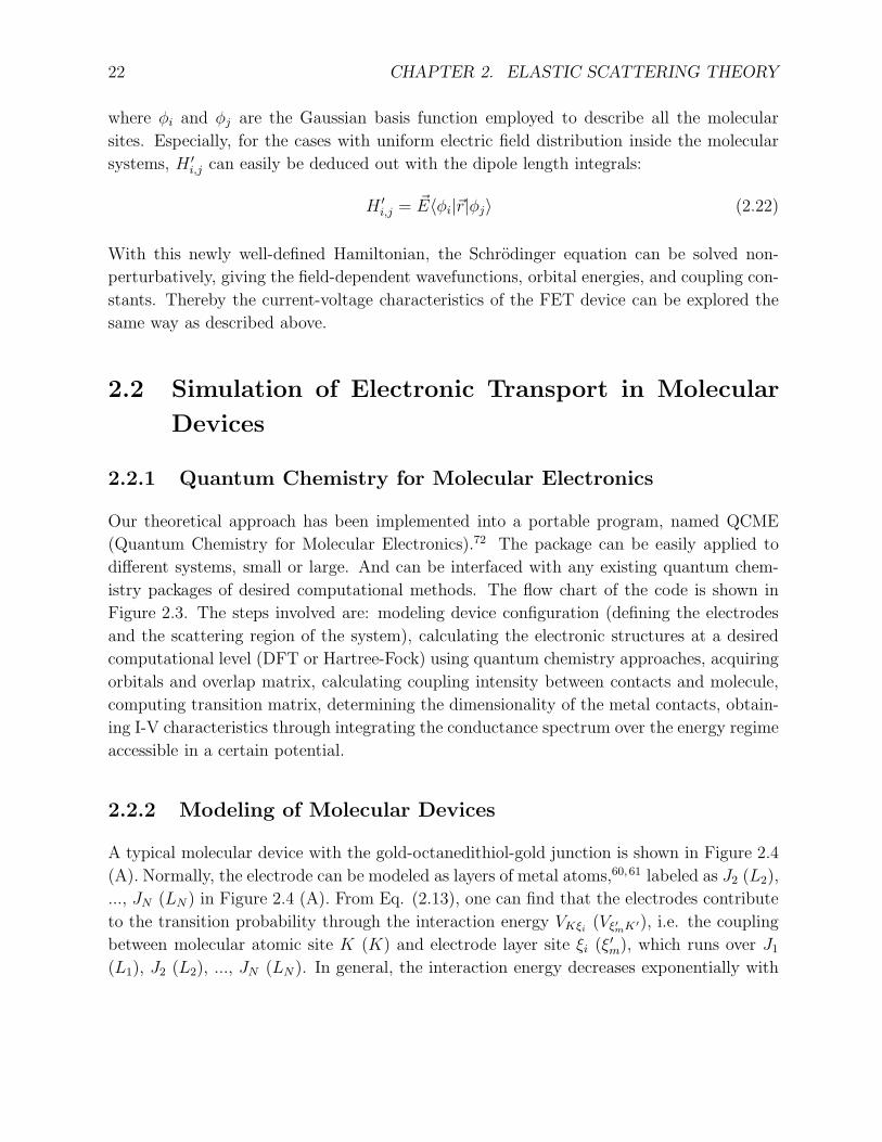
Our theoretical approach has been implemented into a portable program, named QCME
(Quantum Chemistry for Molecular Electronics).72 The package can be easily applied to
different systems, small or large. And can be interfaced with any existing quantum chem-
istry packages of desired computational methods. The flow chart of the code is shown in
Figure 2.3. The steps involved are: modeling device configuration (defining the electrodes
and the scattering region of the system), calculating the electronic structures at a desired
computational level (DFT or Hartree-Fock) using quantum chemistry approaches, acquiring
orbitals and overlap matrix, calculating coupling intensity between contacts and molecule,
computing transition matrix, determining the dimensionality of the metal contacts, obtain-
ing I-V characteristics through integrating the conductance spectrum over the energy regime
accessible in a certain potential.
2.2.2 Modeling of Molecular Devices
A typical molecular device with the gold-octanedithiol-gold junction is shown in Figure 2.4
(A). Normally, the electrode can be modeled as layers of metal atoms,60,61 labeled as J2 (L2),
..., JN (LN ) in Figure 2.4 (A). From Eq. (2.13), one can find that the electrodes contribute
to the transition probability through the interaction energy VKξi(Vξ′mK ′), i.e. the coupling
between molecular atomic site K (K) and electrode layer site ξi (ξ′m), which runs over J1
(L1), J2 (L2), ..., JN (LN ). In general, the interaction energy decreases exponentially with

2.2. SIMULATION OF ELECTRONIC TRANSPORT IN MOLECULAR DEVICES 23
Figure 2.3: Flow chart of QCME code.
increase of the distance between sites. Our numerical calculations of a real molecular device
show that VKJ1(VL1K ′) is always much larger than VKJ2
(VL2K ′). Therefore, it might be
reasonable to assume that metal layers not being connected to the molecule contribute little
to the electron tunneling process.
In addition, numerical calculations prove that the wavefunctions of metal atoms are largely
localized, i.e., removing of a certain metal layer would not change the local wavefunctions of
its neighboring metal layers.73 Periodic calculations for benzenedithiol molecule adsorbed
on Au(111) surface have shown that the electronic density of the electrode close to the
Fermi energy level is mostly localized on the first metal layer connected to the molecule,74
as demonstrated in Figure 2.5. Therefore, the use of small gold cluster to describe the
interaction between molecule and electrode might be a reasonable approximation. In most
of the studies presented in this thesis, the extended molecular model, which contains the
molecule and small gold clusters that resemble the Au(111) surface,21 has also been adopted.
The remaining part of the electrodes is described by an effective mass approximation (EMA).
The extended molecule is then in the equilibrium with the source and the drain through
the line up of their effective Fermi levels. With the known Fermi energy, one can easily
obtain the density of the states of the electrodes with the effective mass approximation.

24 CHAPTER 2. ELASTIC SCATTERING THEORY
Figure 2.4: Structures with full electrode model (A) and three-gold clusters model (B) of
the gold-benzene-gold junction.
This method is quite general and is not limited by the size of the system.
2.2.3 Conducting Channel of Bare and Extended Molecules
As mentioned above, the incoming and outgoing electrons in molecular devices are scattering
through the same molecular orbital. Electrons in the source electrode will be driven to the
drain electrodes by the external electric bias. At the electrode-molecule conjunctions, if the
incoming electron holds energy equal to the energy of a certain molecular orbital, the electron
will be scattered through that orbital. Therefore, molecular orbitals serve as the conducting
Figure 2.5: (A) Benzene molecule connected to a 3×3 surface unit cell of Au (111); (B)
calculated electronic density of the molecular orbital close to the Fermi level.

2.2. SIMULATION OF ELECTRONIC TRANSPORT IN MOLECULAR DEVICES 25
channel in the electron transport process. The characters of the molecular orbitals thus
determine the shape of the I-V characteristics of the molecular devices. In this context, the
knowledge of the energy structure of a molecular device is very crucial to understand the
electron transport mechanism.
In order to take into account the interaction between molecule and electrodes, an extended
molecule, which consists of the bare molecule and metal clusters, is always needed. In
this section, we will discuss orbitals of bare and extended molecules. Bonding schemes for
two molecules bridged between two gold surfaces calculated at the hybrid DFT level are
illustrated in Figure 2.6, where only the outermost orbitals are presented. These bonding
pictures can be explained by the Dewar, Chatt and Duncanson (DCD) model.75,76 In this
model, the interaction between molecule and metal electrodes is viewed as the donation of
a charge from the HOMO of the molecule to the metal and as back donation from the filled
metal states into the LUMO of the molecule. This can be verified from an analysis of the
orbital symmetry for the bare and extend molecules. In Figure 2.6 (A), the LUMO (HOMO)
of the bare molecule were labeled as LUMO-b (HOMO-b), while that of the gold surfaces
were labeled as -Au. It is found the LUMO-b of C6H4S2 with π symmetry interacted with the
HOMO-Au and formed the HOMO and LUMO for the extended molecule Au3 −C6H4S2 −
Au3, which also holds the π symmetry. Meanwhile, the HOMO-b of C6H4S2 coupled with
LUMO-Au build the LUMO+1 and HOMO-1 orbitals. Similar bonding formations have
been observed for all orbitals of Au3 − C6H4S2 −Au3 and Au3 − C8H8S2 −Au3.
From Eq. (2.12) and (2.13), one can see that the larger the projection of the molecular
site Kη in the eigenstate Ψη, the larger the transport probability for that site. Thus it is
expected that in order to contribute significantly to electron conduction, the orbitals must be
delocalized so that the wavefunctions of the orbitals extend over all the sites of the molecule,
i.e., having a large value of 〈Ψη | Kη〉. Since the end molecular sites in connection with the
contact often has the strongest coupling with the contact, the projection of the end sites 1
and N can represent the conducting ability of the molecular orbital. Numerical calculations
indicated that the LUMO+1 for the extended molecule Au3−C6H4S2−Au3 has the strongest
conducting ability in the outermost orbitals,25 and that this LUMO+1 origins from the
HOMO of the bare molecule. Also, HOMO-b in the bare molecule C8H8S2 build unoccupied
orbitals in the extended molecules by interacting with gold surfaces, which conduct electrons.
For both molecules, the HOMO of the bare molecule is the most conductive channel.
2.2.4 Application
In this section, we present our calculated results on several molecular junctions and field
effect transistors that have been fabricated and measured by different experimental groups.

26 CHAPTER 2. ELASTIC SCATTERING THEORY
Figure 2.6: Bonding scheme for molecular adsorption on gold surfaces. (A) Benzene-1,4-
dithiol, (B) α,α′-xylyl dithiol.
Geometry optimization and electronic structure calculations for the extended molecular
systems have been done with Gaussian 03 program.77 The CIS method at the hybrid
density functional theory (DFT) B3LYP78 level and all electron transport properties are
computed using the QCME code.72
I-V Characteristics
The metal-benzene-1,4-dithiol-metal system (shown in Figure 2.4) has served as the model
system in numerous experimental and theoretical studies in the field of molecular electronics.
Here, we have also tested our approach on this famous system.24 Experimentally measured
I-V characteristics of this device have been reported by two groups. In 1997, Reed’s group
manufactured gold-benzene-1,4-dithiol-gold17 and reported clear I-V curves, as shown in
Figure 2.7 (A). Very recently, an experimental study for this system was also performed
by Xiao et al.79 Their measured I-V curve is shown in Figure 2.7 (B). The obtained in
the latter experiment current is about two orders of magnitude larger than that of the
previous one. In general, the solid state physics approaches overestimate the current by
order of magnitudes,9,16 which probably is caused by the significant difference between

2.2. SIMULATION OF ELECTRONIC TRANSPORT IN MOLECULAR DEVICES 27
Figure 2.7: Experimentally (A)17 and (B)79 measured current and conductance as a function
of external bias in benzene-1,4-dithiolate molecular device. (A.1) and (B.1) show theoret-
ically computed results for molecular junctions with Au-S bond length set to 2.984 A and
2.788 A, respectively.
theoretical and experimental geometries.80,81 The big difference between two experiments
can also be attributed to the different metal-molecule bonding configurations involved. In
the experiment of Reed et al.,17 the molecular junction is formed by pushing the metal
electrodes together to allow the molecule being connected with them, while the molecular
junction of Xiao et al.79 is fabricated by pulling a gold STM tip out of the gold substrate.
Both pushing and pulling processes were stopped once the bonding between the gold and the
thiol-end group was established. Therefore, one can expect that the Au-S bond distance in
the molecular junction of Reed et al. should be longer than that in the device of Xiao et al.,
while the optimized geometry sits in between. With the optimized Au-S bond distance as
R(Aus−S)=2.32A (from the sulfur atom to the surface of electrode), our calculated current
is found to be indeed in the middle of the two experimental results,24 which is bout 10 times
bigger than the result of Reed et al..,17 and 10 times smaller than that of Xiao et al.79
Therefore, it seems to be possible to reproduce both experiments if an appropriate bonding
situation is found. Setting R(Aus − S)=2.48A, I-V and S-V curves have been computed
and plotted in Figure 2.7 (A.1), these fit Reed’s results very well. Also, good agreement
to Xiao’s results could be obtained if AU-S bonds were fixed to be R(Aus − S)=2.24A, as
shown in Figure 2.7 (B.1). It is also noted that the shape of the calculated I-V curves fit
quite well with the experimental result of Reed et al.17

28 CHAPTER 2. ELASTIC SCATTERING THEORY
Length Dependence
The relationship between conductance and molecular length is one of the most important
parameters in describing the performance of the molecular devices. The general consensus
is that the coherent current decreases exponentially with the increase of the molecular
length following the relationship, I = I0 exp(−βd), where β is the electron tunneling decay
rate. Length dependence studies have been performed on two interesting molecular systems,
alkanmonothiol(H(CH2)nS) and alkanedithiol (S(CH2)nS), in many experiments.82–85 It was
found that for alkanmonothiol the β value is in the region of 0.6 to 0.94 A−1,82–85 while for
alkanedithiol, the acquired decay rate is significantly smaller than that for alkanemonothiol
junctions.86,87
With the extended molecule model shown in Figure 2.8, we have computed the I-V curves of a
series of alkane molecular junctions: metal-alkanedithiol-metal (gold-[S(CH2)nS]-gold, n=8-
14) and metal-alkanemonothiol-metal (gold-[H(CH2)nS]-gold, n=8-14).26 The calculated
current-voltage (I-V) characteristics of two alkanemonothiol junctions: Au3-H(CH2)8S-Au3
and Au3-H(CH2)10S-Au3 are shown in Figure 2.9 (A) and (B) together with the results of
their experimental counterparts.84 Good agreement between theory and experiment is ob-
tained for both shape and magnitude. Moreover, calculated I-V curves for two alkanedithiol
junctions Au3-S(CH2)8S-Au3 and Au3-S(CH2)12S-Au3 have been shown in Figure 2.9 (C)
and (D), which also agree quite well with the corresponding experimental results.86,87 For
the two alkanedithiol junctions (n=8,12), we have also performed gradient corrected DFT
calculations at the BLYP level with the GAUSSIAN03 program.77 The I-V curves at the
BLYP level shown by the dash dotted lines in Figure 2.9 (C) and (D) are found to have
similar shape as those of B3LYP results, but with larger current values (about 2 times),
which can be attributed to smaller energy gaps given by BLYP method. Nevertheless, it
might be reasonable to state that the I-V characteristics of the molecular devices under
investigation are not very sensitive to the choice of functionals.
Other than I-V characteristics, the length dependence of conducting ability in both systems
have been studied in detail. The calculated resistance as function of CH2 units in alka-
nedithiol junctions under 1.0V bias indeed obey the exponential relation. The β value under
this condition is found to be 0.30/CH2, which is close to the measured value of 0.47/CH2 by
Cui et al.87 Meanwhile, the β value of 0.60/CH2 for alkanemonothiol junctions is obtained,
which is also close to the value of 0.8 /CH2 obtained by Cui et al.84 but smaller than that
from other experimental measurements82,83, 85 (from 0.96/CH2 to 1.25/CH2). A better agree-
ment is found for the ratio between the β values of the alkanemonothiol and alkanedithiol
junctions, which is about 1.93 from our calculations and 1.70 from the experiments of Cui
et al.84,87

2.2. SIMULATION OF ELECTRONIC TRANSPORT IN MOLECULAR DEVICES 29
Figure 2.8: Structures of gold-alkanemonothiol-gold (A) and gold-alkanedithiol-gold (B)
molecular devices.
Figure 2.9: Current-voltage characteristics (on a log scale) of Au3-H(CH2)nS-Au3 system
(upper): (A) Au3-H(CH2)8S-Au3; (B) Au3-H(CH2)10S-Au3 and Au3-S(CH2)nS-Au3 system
(lower): (C) Au3-S(CH2)8S-Au3; (D) Au3-S(CH2)12S-Au3. The B3LYP, BLYP and experi-
mental results are presented by dashed, dash dotted and solid lines, respectively.

30 CHAPTER 2. ELASTIC SCATTERING THEORY
Table 2.1: Calculated products of the coupling energy between the end sites (1 and N) of
molecule and reservoirs (S and D) (V1SVDN), Fermi energy (Ef), and position of the first
conducting orbital (εcon) for alkanemonothiol and alkanedithiol junctions.
Alkanemonothiol n=8 n=10 n=12 n=14
V1SVDN (eV 2) 0.013 0.013 0.013 0.011
Ef (eV ) 4.90 4.89 4.88 4.88
εcon (eV ) 6.19 6.17 6.16 6.15
Alkanedithiol n=8 n=10 n=12 n=14
V1SVDN (eV 2) 0.169 0.1691 0.168 0.168
Ef (eV ) 4.91 4.91 4.90 4.90
εcon (eV ) 6.17 6.18 6.17 6.17
Figure 2.10: Summation of terminal sites contribution (on a log scale) (〈1 | η〉〈η | N〉)2 from
20 unoccupied orbitals as a function of the number of carbons for alkanemonothiol (square
dots and curve A) and alkanedithiol (triangle dots and curve B) junctions.

2.2. SIMULATION OF ELECTRONIC TRANSPORT IN MOLECULAR DEVICES 31
Figure 2.11: (a) Structures of three devices consisting of the phenyl-I, phenyl-II and phenyl-
III molecules, respectively. (b) A semi-log plot of the calculated resistance at the external
bias of 0.1 V as a function of number of phenyl groups.
To reveal the reasons behind the difference between the β of alkanedithiol and alkanemonoth-
iol junctions, three key parameters determining the transition probability T , namely the
coupling energy V , the conducting orbital energy εη and the site contribution 〈J | η〉, have
been analyzed. The products of coupling energy between the first site 1 and source reser-
voir S and coupling energy between the drain reservoir D and end site N (V1SVDN), the
calculated Fermi energy (EF ) and the orbital energy of the first conducting orbital εcon for
alkanedithiol and alkanemonothiol junctions are listed in Table 2.1. As expected, these pa-
rameters converge very fast with respect to the molecular length for both systems. However,
strong length dependence has been found for site contribution 〈J | η〉. In Figure 2.10, the
terminal site contributions (〈1 | η〉〈η | N〉)2 from 20 unoccupied orbitals as a function of
number of carbons are given. It can be seen that such a contribution decreases exponen-
tially with respect to the molecular length with a decay rate of -1.6 and -2.3 for alkanedithiol
and alkanemonothiol junctions, respectively. It seems like that the metal-molecule bonds
can effectively enhance the delocalization of the conducting orbitals of short alkanedithiol
chains and result in a large difference in the electron decay rates for alkanedithiol and
alkanemonothiol junctions.
Another well studied molecular system is self-assembled monolayers of oligophenylene.83,88
Three gold-oligophenylene-gold devices with one, two and three benzene units are illustrated
32 CHAPTER 2. ELASTIC SCATTERING THEORY
in Fig. 2.11 (a), labeled as phenyl-I, phenyl-II and phenyl-III, respectively. One can see
that one of the electrode in the device is chemically bonded to the molecule while the other
is only physically absorbed to the Hydrogen atom at the end of the molecule. Effects of
metal-molecule distances on the current-voltage characteristics of three devices have been
examined, and the distances that reproduce the experimental results for all three devices are
found to be R(Aus −S)=2.32A (from the sulfur atom to the surface of electrode), R(Aus −
H)=1.25A. Such a Au-S bond distance is the same as the one used in our previous study on
benzendithiol devices.25,26 With the fixed metal-molecule bond lengths, our calculated I-V
characteristics26 are in excellent agreement with all experimental results.83 In Figure 2.11
(b), it is shown that the length dependent resistance (dI/dV) follows the exponent decay
rule, R = R0 exp(−βd). At external bias of 0.1 to 0.25 V, our calculated decay rate is always
around β=1.76/phenyl, exactly the same as the experimental value.83
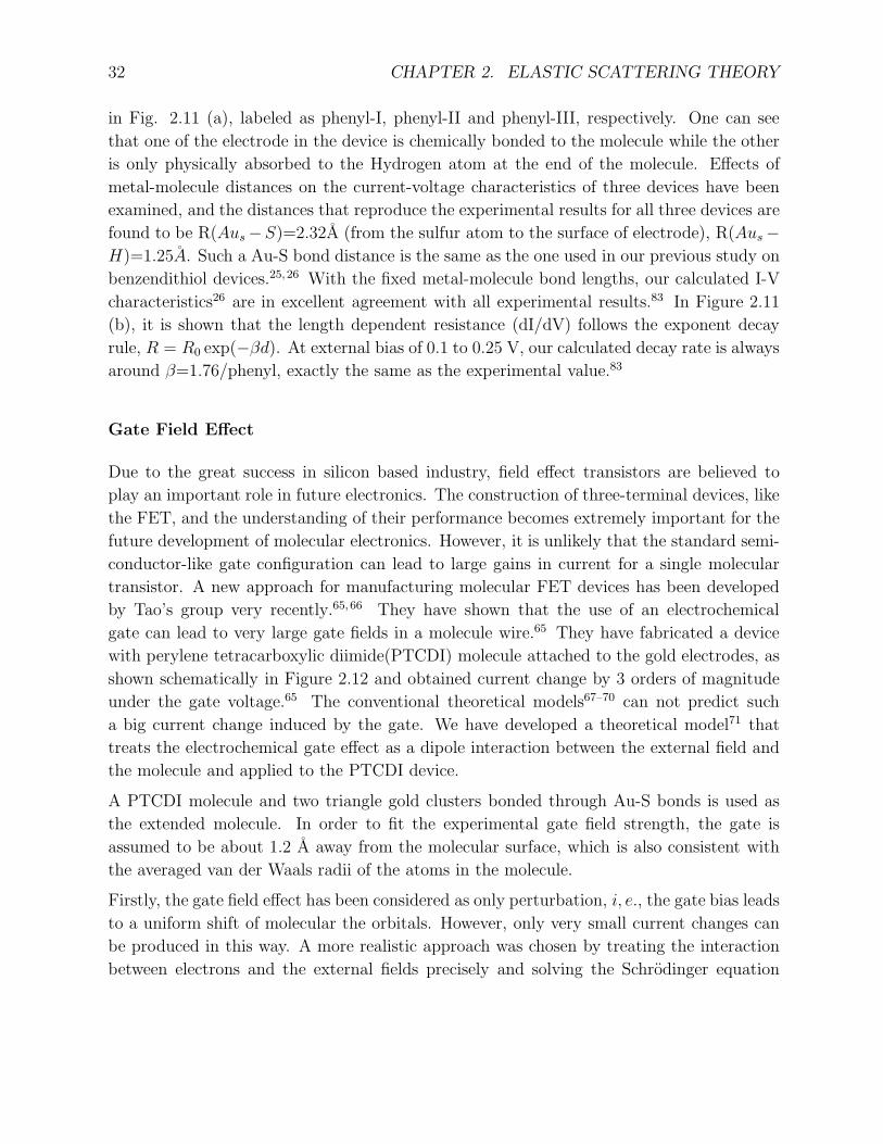
Gate Field Effect
Due to the great success in silicon based industry, field effect transistors are believed to
play an important role in future electronics. The construction of three-terminal devices, like
the FET, and the understanding of their performance becomes extremely important for the
future development of molecular electronics. However, it is unlikely that the standard semi-
conductor-like gate configuration can lead to large gains in current for a single molecular
transistor. A new approach for manufacturing molecular FET devices has been developed
by Tao’s group very recently.65,66 They have shown that the use of an electrochemical
gate can lead to very large gate fields in a molecule wire.65 They have fabricated a device
with perylene tetracarboxylic diimide(PTCDI) molecule attached to the gold electrodes, as
shown schematically in Figure 2.12 and obtained current change by 3 orders of magnitude
under the gate voltage.65 The conventional theoretical models67–70 can not predict such
a big current change induced by the gate. We have developed a theoretical model71 that
treats the electrochemical gate effect as a dipole interaction between the external field and
the molecule and applied to the PTCDI device.
A PTCDI molecule and two triangle gold clusters bonded through Au-S bonds is used as
the extended molecule. In order to fit the experimental gate field strength, the gate is
assumed to be about 1.2 A away from the molecular surface, which is also consistent with
the averaged van der Waals radii of the atoms in the molecule.
Firstly, the gate field effect has been considered as only perturbation, i, e., the gate bias leads
to a uniform shift of molecular the orbitals. However, only very small current changes can
be produced in this way. A more realistic approach was chosen by treating the interaction
between electrons and the external fields precisely and solving the Schrodinger equation

2.2. SIMULATION OF ELECTRONIC TRANSPORT IN MOLECULAR DEVICES 33
Figure 2.12: Model device of PTCDI molecule in contact with two Au electrodes.
Figure 2.13: Experimental data65 (a) and our theoretical simulation (b) of current through
source and drain Isd as the function of gate voltage Vg in a single PTCDI molecule transistor.
non-perturbatively. The interaction energy was represented as the potential in the real
space. Calculations show that the permanent dipole moment of the molecule is quite small,
it is found to be 0.01, 0.14, and 0.03 Debye for the three components of the permanent
dipole moment of the molecule-gold complex, µx, µy, and µz, respectively. However, the
induced polarization of the molecule is included in our non-perturbative approach which is
found to have strong impact on the I-V characteristics of the device. Although small dipole
moments were found in the PTCDI molecule, a very large polarizability can be expected due
to the strong conjugation. Our calculations indicated that the polarizability of the PTCDI
molecule has three large diagonal components with values of 1072, 388 and 223 a.u. for αxx,
αyy and αzz, respectively. Thus, the molecular orbitals are heavily perturbed by the external
electric field89 through the polarization, as clearly shown by the following simple energy
expression, ǫa = ǫa0 − µaiEi −
12αa
ijEiEj .... Here ǫa0 and ǫa are the energy of orbital a without
and with electric field Ei, respectively. µai and αa
ii are the dipole moment and polarizability
of orbital a, respectively. With the external electric field and large polarizability of the
molecule, strong gate effects can be anticipated.
One of the advantages of theoretical simulations is to examine the effects of different gate

34 CHAPTER 2. ELASTIC SCATTERING THEORY
configurations, which are difficult to control in the experiment.65 Many different configu-
rations have been tested numerically and only one particular configuration provides results
that fits well to experiments as presented in Figure 2.13. In this configuration, the source-
drain field is oriented 150o with respect to the X axis in the X-Z plane and can be described
by a vector (-0.87,0,0.5). As one can see from Figure 2.13, the agreement between theory
and experiment is very good. Both the absolute values and shapes of the Isd-Vg curves
are consistent with experiment. In the region of gate voltage from 0.7 to 0.8 V, a plateau
observed in the experiment has also been reproduced by our simulations. It also indicates
that the molecular orbitals are not shifted linearly with respect to the increase of the gate
voltage. In this device, molecular orbitals are largely affected by the strength and direction
of the electric field, rather than by the voltage itself.

Chapter 3
Inelastic Scattering Theory
Inelastic electron tunneling spectroscopy (IETS) was developed in the 1960s to study vibra-
tional spectra of organic molecules buried inside metal-oxide-metal junctions and has since
become a powerful spectroscopic tool for molecular identification and chemical bonding in-
vestigations.28–30 Investigation with IETS have had significant technological implications
because they give structural information about the molecular junction and provide a direct
access to the dynamics of energy relaxation and thermal dissipation during the electron
tunneling.
3.1 Theory
Also our approach for inelastic scattering is based on the Green’s function formalism. The
molecular device was decomposed into three parts, the source, the drain and the extended
molecule, as shown in Figure 2.1. Generally speaking, when energetic constraints are satis-
fied, the electron crossing the junction may exchange a definite amount of energy with the
molecular nuclear motion, resulting in an inelastic component in the transmission current.90
To describe the electron-vibronic coupling effect, molecular theory based on vibrational nor-
mal modes has been introduced to our scattering model. In the adiabatic Born-Oppenheimer
approximation, the purely electronic Hamiltonian of the molecular systems can be consid-
ered parametrically as dependent on the vibrational normal modes Q. The one-electron
Hamiltonian can then be partitioned as
H(Q) = H(Q, e) +Hν(Q) (3.1)
35

36 CHAPTER 3. INELASTIC SCATTERING THEORY
where H(Q, e) and Hν(Q) are the electronic and the vibrational Hamiltonian, respectively,
so that the Schrodinger Equation becomes
[H(Q, e) +Hν(Q)] | Ψη(Q, e)〉 | Ψν(Q)〉
= H(Q, e) | Ψη(Q, e)〉 | Ψν(Q)〉 +Hν(Q) | Ψν(Q)〉 | Ψη(Q, e)〉
= (εη +∑
a
nνahωa) | Ψη(Q, e)〉 | Ψν(Q)〉 (3.2)
where εη represent the energy of eigenstate η of the pure electronic Hamiltonian, ωa is the
vibrational frequency of vibrational normal modes Qa, and nνa is the quantum number for
the mode Qa in | Ψν(Q)〉.
By using a Taylor expansion, the nuclear motion depended wavefunction can be expanded
along each vibrational normal mode. Since most IETS are measured at the electronic off-
resonant region (where conducting levels are far from the Fermi energy), the adiabatic
harmonic approximation can be applied. We can then use the first derivative like ∂Ψ(Q)∂Qa
to represent the vibrational motion part in the wavefunctions.90 Therefore, the vibrating
depended wavefunction along an eigenstate εη is described as
| Ψη(Q, e)〉 | Ψν(Q)〉 =| Ψη0 |Q=0 +
∑
a
∂Ψη0
∂QaQa |Q=0 + ...〉 | Ψν(Q)〉 (3.3)
where | Ψν(Q)〉 is the vibration wavefunction. Ψη0 is here the intrinsic electronic wavefunction
at the equilibrium position, Q0.
Following the process described in Chapter (2), the electron transition moment can be
extended to describe the inelastic elastic electron scattering process. The transition matrix
element from the source to the drain, T (VD, Q), can now be generalized by taking into
account the vibrational motion (Q) into Eq. (2.13).
T (VD, Q) =∑
J
∑
K
VJS(Q)VDK(Q)
×∑
η
∑
ν′,ν,ν′′
〈Jη(Q, e) |1
zη −H(Q)| Ψη,ν(Q)〉〈Ψη,ν(Q) | Kη(Q, e)〉
=∑
J
∑
K
VJS(Q)VDK(Q)∑
η
∑
ν′,ν,ν′′
gη,ν′,ν,ν′′
JK (3.4)

3.1. THEORY 37
Applying the vibrational normal mode theory, we have
gη,ν′,ν,ν′′
JK = 〈Ψν′
(Q) | 〈Jη(Q, e) |1
zη −H(Q)| Ψη,ν(Q)〉〈Ψη,ν(Q) | Kη(Q, e)〉 | Ψν′′
(Q)〉
= 〈Ψν′
(Q) | 〈Jη(Q, e) |1
zη − εη +∑
a nνahωa
| Ψη,ν(Q)〉〈Ψη,ν(Q) | Kη(Q, e)〉 | Ψν′′
(Q)〉
=〈Ψν′
(Q) | 〈Jη(Q, e) | Ψη(Q, e)〉 | Ψν(Q)〉〈Ψν(Q) | 〈Ψη(Q, e) | Kη(Q, e)〉 | Ψν′′
(Q)〉
zη − εη +∑
a nνahωa
(3.5)
in which the first term can be computed by
〈Ψν′
(Q) | 〈Jη(Q, e) | Ψη(Q, e)〉 | Ψν(Q)〉
= 〈Ψν′
(Q) | 〈Jη0 +
∑
b
∂Jη0
∂Qb
Qb | Ψη0 +
∑
a
∂Ψη0
∂Qa
Qa〉 | Ψν(Q)〉
= 〈Ψν′
(Q) | 〈∑
b
∂Jη0
∂QbQb |
∑
a
∂Ψη0
∂QaQa〉 | Ψν(Q)〉 + 〈Ψν′
(Q) | Ψν(Q)〉〈Jη0 | Ψη
0〉
+ 〈Jη0 |
∑
a
∂Ψη0
∂QaQν′ν
a 〉 + 〈∑
b
∂Jη0
∂QbQν′ν
b | Ψη0〉 (3.6)
Here the 〈∑
b∂Jη
0
∂QbQb |
∑a
∂Ψη0
∂QaQa〉 terms have very small numerical magnitude so that the
first term can be neglected.
It is assumed that electrons scatter from the ground state in the source reservoir to an
excitation level, and transport through that conducting channel to the ground state in the
drain reservoir. The ground state is not a conducting channel. Therefore, assuming the
nuclear motion is harmonic, we have
〈Ψν′
(Q) | Ψν(Q)〉〈Jη0 | Ψη
0〉 = 〈ν ′ | ν〉〈Jη0 | Ψη
0〉 = 〈0 | 1〉〈Jη0 | Ψη
0〉 = 0 (3.7)
and
Qν′νa = 〈ν ′ | Qa | ν〉 = 〈0 | Qa | 1〉 =
√h
2ωa(3.8)

38 CHAPTER 3. INELASTIC SCATTERING THEORY
Therefore, gη,ν′,ν,ν′′
JK can be rewritten as
gη,ν′,ν,ν′′
JK =1
zη − εη −∑
a nνahωa
× [〈Jη0 |
∑
a
∂Ψη0
∂QaQν′ν
a 〉 + 〈∑
b
∂Jη0
∂QbQν′ν
b | Ψη0〉]
× [〈Kη0 |
∑
c
∂Ψη0
∂QcQνν′′
c 〉 + 〈∑
d
∂Kη0
∂QdQνν′′
d | Ψη0〉] (3.9)
Using A, B, C, and D to represent the above four terms 〈Jη0 |
∑a
∂Ψη0
∂QaQν′ν
a 〉, 〈∑
b∂Jη
0
∂QbQν′ν
b |
Ψη0〉, 〈K
η0 |
∑c
∂Ψη0
∂QcQνν′′
c 〉, and 〈∑
d∂Kη
0
∂QdQνν′′
d | Ψη0〉, the equation can be simplified to be
gη,ν′,ν,ν′′
JK = (A+B)(C +D)/(zη − εη −∑
a
nνahωa) (3.10)
If the interference effect between different sites are neglected, i.e., if the parameter zη for
injecting energy and escape rate for electrons have no site dependence, by going through all
of molecular sites the formula can be approximated to
∑
JK
gη,ν′,ν,ν′′
JK = (A+B)(C +D)/(zη − εη −∑
a
nνahωa)
= 2 × A× (C +D)/(zη − εη −∑
a
nνahωa) (3.11)
The inclusion of nuclear motion introduces vibrational excited states in the electronic ground
state potential. These vibrational excited states are the ones that contribute to the inelastic
terms in the case of off-resonant excitation. Meanwhile, the electron can also tunnel through
the molecular orbitals, resulting in the elastic term in the total current. In this case, the
transition matrix element from the source to the drain can be written as
T (VD, Q)el =∑
J
∑
K
VJS(Q)VDK(Q)∑
η
gη,0,0,0JK (3.12)
where
gη,0,0,0JK = 〈0 | 〈Jη(Q, e) |
1
zη −H(Q)| Ψη,0(Q)〉〈Ψη,0(Q) | Kη(Q, e)〉 | 0〉
=〈0 | 〈Jη(Q, e) | Ψη(Q, e)〉 | 0〉〈0 | 〈Ψη(Q, e) | Kη(Q, e)〉 | 0〉
zη − εη(3.13)
Again, the first term can be computed by

3.1. THEORY 39
〈0 | 〈Jη(Q, e) | Ψη(Q, e)〉 | 0〉
= 〈0 | 〈Jη0 +
∑
b
∂Jη0
∂Qb
Qb | Ψη0 +
∑
a
∂Ψη0
∂Qa
Qa〉 | 0〉
= 〈0 | 〈∑
b
∂Jη0
∂QbQb |
∂∑
a Ψη0
∂QaQa〉 | 0〉 + 〈0 | 0〉〈Jη
0 | Ψη0〉
+ 〈Jη0 |
∑
a
∂Ψη0
∂QaQ00
a 〉 + 〈∑
b
∂Jη0
∂QbQ00
b | Ψη0〉 (3.14)
Since Q00a = 〈0 | Qa | 0〉 = 0 and 〈0 | 0〉 = 1, this time only the wavefunction without
vibrational dependence remains, so that the transition matrix element becomes
T (VD, Q)el =∑
J
∑
K
VJS(Q)VDK(Q)∑
η
gηJK,el
gηJK,el =
〈Jη(Q, e) | Ψη(Q, e)〉〈Ψη(Q, e) | Kη(Q, e)〉
zη − εη(3.15)
which is consistent with Eq. (2.12) and (2.13) for the elastic current expressed in the
previous chapter. Therefore, the total current in molecular devices can be decomposed into
two parts
I = Iel + Iinel (3.16)
where Iel and Iinel are the elastic and inelastic contributions to the electron tunneling current,
respectively. Typically, only a fraction of tunneling electrons as involved in the inelastic
tunneling process. The small conductance change induced by the electron-vibronic coupling
is commonly measured by the second harmonics of a phase-sensitive detector for the second
derivative of the tunneling current
d2I/dV 2
or the part normalized by the differential conductance
(d2I/dV 2)/(dI/dV )
It is also very useful to provide spatial distributions of inelastic signal in IETS applications.
Working with the site representation, a very convenient way is to approximate the intensity
of the inelastic signal at position ~r as the nuclear motion dependent part in the wavefunction.
∑
J
∑
a
∂Jη0 (~r)
∂QaQa

40 CHAPTER 3. INELASTIC SCATTERING THEORY
Figure 3.1: Structures of the gold-octanedithiol-gold junction with triangle contacts.
3.2 Applications
In this section, we will present few examples to assess the performance of our formulation for
describing elastic and inelastic electron transport properties of several molecular junctions.
3.2.1 I-V Characteristics
An octanedithiolate molecule, SC8H16S, embedded between two gold electrodes through
S-Au bonds, has been investigated in Paper IV. The extended molecule consists of two
triangle gold trimers bonded with an octanedithiolate molecule, see Figure 3.1. Electronic
structure calculations have been carried out for the extended molecules at the hybrid DFT
B3LYP level78 using the Gaussian03 package with LanL2DZ basis set.77
The calculated electron tunneling current (including both elastic and inelastic parts) are
illustrated as a function of applied bias in Figure 3.2.1 (A), together with the corresponding
experimental I-V curve of Wang et al..29 The shape of the calculated I-V curve agrees
well with experiment. Our calculations are performed for a single molecule system, while
the measurements of Wang et al.29 were done for self-assembly layers consisting of many
molecules. The fact that our calculated current is about two orders of magnitude smaller
than the measured one might indicate that there are more than 100 molecules contributing
to the experimental current value. We have also compared our calculated result with the
measurement for a single molecule of Cui et al.,86,87 see Figure 3.2.1(C). The agreement
between theory and experiment is very good. Furthermore, the experimentally observed

3.2. APPLICATIONS 41
Figure 3.2: Current (on a log scale) of the gold-octanedithiolate-gold device as a function
of voltage. (A): Calculated total electron tunneling current (include both elastic and in-
elastic contributions) under different working temperatures. (B): Current measured under
different working temperatures by Wang et.al.29 (C): Experimental result of Cui86,87 (Solid
line), calculated elastic current (dotted line), and calculated total current (dashed line) at
temperature 300K.
temperature independent I-V characteristics are also reproduced by our calculations.
3.2.2 Inelastic Electron Tunneling Spectroscopy
IETS dependence on molecular conformation
The calculated inelastic electron tunneling spectroscopy (IETS) of the octanedithiolate junc-
tion with the triangle gold trimers are shown in Figure 3.3, together with the experimental
spectrum of Wang et al. at temperature 4.2 K.29 One can clearly see that the calculated
result for the triangle configuration is in good agreement with the experiment. The calcu-
lations do not only reproduce all the major spectral features observed in the experiment,
but also provide very detailed features that were smeared out by the background due to the
encasing Si3N4 in the experiment.29 Our computational scheme also allows to calculate the
spectral linewidth directly, which is determined by the orbital characters and the molecule-
metal bonding, see Eq. (2.11). The calculated full width at half maximum (FWHM) for the
spectral profile of mode ν(C-C) at 132 mV is found to be around 6.1 meV, to be compared
with the experimental result of 3.73±0.98 meV.29
We have also calculated the IETS of the gold chain configuration, to examine the dependence
of the IETS on the molecule-metal bonding structure. Indeed, the IETS of chain contacts
shows a distinct difference in the spectral intensity distribution from that of the triangle
configuration. The changes in molecular conformations seem to be the major cause for the
large difference in the spectral intensity distributions of the two devices. It is interesting

42 CHAPTER 3. INELASTIC SCATTERING THEORY
Figure 3.3: Inelastic electron tunneling spectrum of the octanedithiol junction. Dashed
line from experiment,29 and solid line for our simulation based on the triangle contact
configuration. The working temperature is 4.2 K. Star marks for background signal in the
experiment.
to note that the spectrum of the chain configuration resembles quite well the experimental
IETS of an alkanemonothiol molecule, HS(CH2)8H (C11).28 One can thus conclude that
the large difference in the experimental spectral intensity distributions28,29 related to the
molecular vibrational modes implies that the molecular conformations in two experimental
setups are different.
IETS spatial distribution
One very useful way to understand the electron-vibration coupling is through the imaging
of spatial distribution of an IETS signal. Starting with an important experiment by Stipe
et al.,91 IETS with scanning tunneling microscope (STM), IETS-STM, has become an es-
tablished technique to probe the local vibrational density.31,92–94 The vibrational spectral
profiles reveal information about the symmetry and strength of electron-phonon coupling.
In a recently joint experimental and theoretical study on IETS-STM of Gd@C82 molecules,

3.2. APPLICATIONS 43
Figure 3.4: Calculated IETS spatial maps for vibrational modes of the OPE-NO2 molecule
with frequencies 1246.5 (A), 2233.1 (B), and 3202.5 (C) cm−1, and maps for vibrational
modes of OPE with frequencies 2231.2 (D) and 3201.4 (E) cm−1.
Figure 3.5: Calculated IETS spatial maps for vibrational modes of Au3-OPE-NO2-Au3 with
frequencies 1246.1 (A), 2230.7 (B), and 3202.9 (C) cm−1, and maps for vibrational modes
of Au3-OPE-Au3 with frequencies 2227.8 (D) and 3202.4 (E) cm−1.
Grobis et al.31 found that the inelastic single is mostly spatially localized and detectable
only on certain parts of Gd@C82 molecule. With our theoretical approach, we can also
simulate IETS-STM images of molecular devices.
IETS of oligophenylenethynylene (OPE) molecule has been studied both experimentally
and theoretically.28,95 Our theoretical approach has also been applied to this system and
successfully reproduced the experimental IETS spectrum.34 Here, we illustrate spatial dis-
tributions of certain vibrational modes appearing in IETS of the OPE molecule. Effects
of electron acceptor (NO2) and metal clusters on electron-vibration couplings are demon-
strated. All images are shown in Figs. 3.4 and 3.5. In Fig. 3.4 (A), the image of the
vibrational mode at frequency 1246.5 cm−1 is given. It can be seen that the spectral feature
of this vibrational mode is mostly localized on the N-O bonds. Spatial maps of vibrational
modes at frequencies 2233.1 and 3202.5 cm−1 of OPE-NO2 are given in Fig. 3.4 (B) and

44 CHAPTER 3. INELASTIC SCATTERING THEORY
(C), respectively. The localization behavior of these vibrational modes are clearly illus-
trated. The same vibrational modes for the pure OPE molecule are presented in Fig. 3.4
(D) and (E) for comparison. The effect of the NO2 group has negligible contribution to the
images of these two vibrational modes. Furthermore, the presence of gold clusters does not
have noticeable impact on the images of these two vibrational modes as evident in Fig. 3.5.
These images indicate that the localization of nuclear motions of the atoms can result in
the localization of the inelastic electron tunneling signal.

Chapter 4
Central Insertion Scheme
4.1 General
Our Central Insertion Scheme (CIS) is based on the simple fact that for a large enough
finite periodic system, the interaction between different units in the middle of the system
should be converged, and consequently those units in the middle become identical. It is
thus possible to elongate the initial system by adding the identical units in the middle of
the system continuously. This can be easily done when the Hamiltonian of the system is
described in the site-representation. Obviously, the prerequisite for using the CIS method
is to obtain an initial Hamiltonian in the site-representation possessing identical central
parts, which can only be achieved by computing a fairly large initial system. Fortunately
this condition can be fulfilled routinely by modern quantum chemistry programs. It should
be stressed that the CIS method should be as accurate as the method used for the initial
system.
We have applied our approach to conjugated polymers, carbon nanotubes (CNT), DNA,
and diamondoid molecules. Comparing to the traditional quantum chemistry methods,
our approach provides results of the same accuracy with only a fraction of computational
time. The biggest nano-scale system being investigated is a three-dimensional hydrogen
terminated diamond cluster that consists of as many as 125000 electrons. The largest one-
dimensional nanostructure is a 200 nm SWCNT, with 16000 carbon atoms described by
150000 Gaussian basis functions.
45

46 CHAPTER 4. CENTRAL INSERTION SCHEME
Figure 4.1: (a): Schematic draw of the geometry (I) and the Hamiltonian matrix (II) of a
n unit periodic structure; (b): The geometry (I) and the Hamiltonian matrix (II) of two
stretched structures copied from (a); (c) The geometry (I) and the Hamiltonian matrix (II)
of the elongated structure with n+ 1 units.
4.1.1 Hamiltonian
We consider a system that consists of two end parts, namely L and M, connected by a peri-
odic structure including n uniform units U1, U2, ..., Un, with geometry shown schematically
in Figure 4.1 (a) I. A one-dimensional structure picture were chosen as an example, but
it should be noted that this approach is independent on the space distribution and can be
applied to any dimensional periodic structures.
In quantum chemistry, to obtain the electronic structure of a molecular system, one only
has to solve the Schrodinger equation:
H | Ψη〉 = εη | Ψη〉 (4.1)
where | Ψη〉 is the wavefunction for the eigenstate εη, and H is the Hamiltonian of the system.
When describing a periodic system, it is more suitable to work in the site representation.

4.1. GENERAL 47
The wavefunctions are expanded in terms of the site basis: | L〉 and |M〉 for the end parts,
and | Ki〉 (i runs over U1, U2, ... , Un) for the center part. Each of them can be described
by a linear combination of atomic orbitals (LCAO):
| A〉 =∑
α
| cAj ψAj 〉
A = L,M,Ki (4.2)
If we define
Hi,j = 〈ψi | H | ψj〉 , Si,j = 〈ψi | ψj〉 (4.3)
where i and j run over sites L, U1, U2, ... , Un, and M, then transfer the equation (4.1) to:
HL,L HL,1 ... HL,n HL,M
H1,L H1,1 ... H1,n H1,M
... ... ... ... ...
Hn,L Hn,1 ... Hn,n Hn,M
HM,L HM,1 ... HM,n HM,M
CηL
Cη1
...
CηN
CηM
= εη
SL,L SL,1 ... SL,n SL,M
S1,L S1,1 ... S1,n S1,M
... ... ... ... ...
Sn,L Sn,1 ... Sn,n Sn,M
SM,L SM,1 ... SM,n SM,M
CηL
Cη1
...
CηN
CηM
(4.4)
where Cηi = (cηi1 c
ηi2 ... c
ηiα)T represent the coefficient submatrices of subsystems L, Ui−1, and
M in the molecular orbital εη, respectively.
4.1.2 Approximations
Three approximations are assumed in the CIS method. The first one is to assume that
the central parts of a sufficiently large system should have converged electronic structures.
Secondly, the convergence of electronic structure should lead to the convergence of charge
densities in the center parts. For instance, for the system described in Figure 4.1 (a)I,
the wavefunction of the mid unit Un2
is approximately the same as that of unit Un2+1, and
the interaction and overlap between Un2
and Un+1
2
are approximately the same as those
between Un+1
2+1 and Un+2
2
. Thirdly, the long range interaction between subsystems can be
neglected. For carbon nanotubes, a distance > 20 A is found to be adequate. It can be
varied depending on the system under investigation.

48 CHAPTER 4. CENTRAL INSERTION SCHEME
Table 4.1: Electron density distribution of the HOMO along the different unit Ui of the
original and the reconstructed PPT10.
Electron density Reconstructed Original Difference
U1 0.0351 0.0357 0.0006
U2 0.0766 0.0771 0.0006
U3 0.1259 0.1251 0.0008
U4 0.1684 0.1657 0.0027
U5 0.1901 0.1847 0.0053
U6 0.1835 0.1864 0.0028
U7 0.1512 0.1550 0.0038
U8 0.1041 0.1086 0.0045
U9 0.0571 0.0603 0.0032
U10 0.0227 0.0242 0.0015
Several small nano-systems have been used to verify the three approximations. One of them
is a 10-units (8nm) conjugated poly(p-phenyleneethynylene) (PPT) (labeled as PPT10).
For polymer systems, the intrinsic periodic unit is chosen as the unit cell Ui in the CIS
method. Using the GAUSSIAN03 program, geometry optimization and electronic structure
calculations for PPT10 have been performed at the DFT B3LYP level with the 6-31G
basis set. Matrices for Hamiltonian, orbital overlap, orbital coefficients, and eigenvalues
that are needed for Eq. (4.4) are obtained. To verify the first two approximations about
the convergence of the electronic structure in the central part of the systems, we have
inter-exchanged two units of Hamiltonian (H) and overlap (S) matrix in the center parts of
PPT10. For instance, the submatrix Hn2,i and Sn
2,i were replaced by (Hn
2,i+Hn
2+1,i+1)/2 and
(Sn2,i+Sn
2+1,i+1)/2, respectively, where i runs over Un
2−4, Un
2−3, Un
2−2, Un
2−1 and Un
2. Similar
rules have also been applied to obtain new submatrice Hi, n2
and Si, n2, Hn
2+1,i and Sn
2+1,i,
Hi, n2+1 and Si, n
2+1. With these reconstructed matrices, a new set of molecular orbitals and
wavefunctions can be obtained, which reproduce the original results from GAUSSIAN03. For
the initial system, energy gap Eg between LUMO and HOMO is found to be 2.784 eV, while
the reconstruction of matrices introduces an error of 0.002 eV. For orbitals from HOMO-20
(-6.925 eV) to LUMO+20 (0.467 eV), the smallest and the biggest errors caused by the
reconstruction are 5.1E-07 and 0.008 eV, respectively. The electron density distribution of
HOMO in different unit Ui of PPT10 obtained from both methods are listed in Table. 4.1,
from which one can notice that the two sets of data are in very good agreement. The same
approach has been tested on CNT21 and shows the same good performance.

4.1. GENERAL 49
Figure 4.2: (a) Structure of a 10-units (8nm) conjugated poly(p-phenyleneethynylene)
(PPT10). (b) 21 layers (5, 5) metallic SWCNT (CNT21). (c) Interaction energy between
U1 and the remaining units in PPT10 (circle dots) and CNT21 (square dots) as a function
of the distance between the units.
To test the third approximation, the interaction energy between two units Ui and Uj have
been calculated using equation (2.5) for PPT10. The length dependent interaction energies
are shown in Figure 4.2 (c). If we look at the interaction energy between U1 and the
remaining units of PPT10, it can be seen that the interaction energy between two sub-units
dies out fairly quick with respect to the distance between them. The same conclusion holds
for other systems under test, like PPT14, 21 layers and 33 layers (5, 5) metallic SWCNTs
(CNT21 and CNT33), and 4 base-pair and 6 base-pair poly(G)-poly(C) DNA (GC4 and
GC6).

50 CHAPTER 4. CENTRAL INSERTION SCHEME
4.1.3 CIS Procedure
In general, the most time consuming step in conventional quantum chemistry approaches is
the SCF (self-consistent-field) cycles to build an accurate Fock matrix for the system under
investigation. Due to the enormous number of electrons involved in the large-nano scale
system, the number of integrals needed to be computed in each SCF cycle is extremely large.
It is thus obvious that the computational time can be significantly shortened if the number
of SCF cycles can be reduced. One of the best ways to reduce the number of SCF cycles is
to have a good initial guess that is close to the final result. This is what CIS method aims to
achieve: providing a very good initial guess. The whole process is quite straightforward, as
can be seen from the schematic picture in Figure 4.1. We firstly calculated Hamiltonian and
electronic structures of an initial system, which should be at least partly periodic and large
enough to have well-converged center parts, as shown in Figure 4.1(a). We then make two
identical initial systems, and put them together as in Figure 4.1(b). From Figure 4.1(b)I,
one can see that two initial structures have been placed side by side but with exactly one
periodic unit mismatched. A new system with n + 1 periodic units (U′′′
i ), shown in Figure
4.1 (c)I, can thus be constructed by simply putting these two n units systems together, i.e.
the system is elongated. We should notice that the use of two identical initial systems is just
to make it simple to describe the elongation process, and there are actually no constraints
on the number of initial systems that can be used. Furthermore, the initial systems do not
always have to be identical, and computational experience proves that initial systems with
partly overlapping identical parts work fine in constructing larger nano-scale systems, as
long as their chemical environments are the same.
The elongation of the geometrical structure thus leads to the elongation of the Hamiltonian
matrix. The way of constructing the corresponding matrices are also schematically shown
in Figure 4.1. In Figure 4.1(a)II, a (n + 2) × (n + 2) matrix (L, Ui, M) has been plotted
to represent the Hamiltonian of the initial system. It should be noted that there are no
limitations on the sizes of the end parts L and M, and the use of one unit to represent
the end part is just for the sake of simplicity. Following the same process in elongating
the geometry, two initial Hamiltonian matrices have been put together as in shown Figure
4.1(b)II, denoted as (L′
, U′
i, M′
) and (L′′
, U′′
i , M′′
), respectively. One of the end parts
of each matrices has been set to zero. Thus, by putting these two systems together with
one unit mismatched, a new (n + 3) × (n + 3) matrix (L′′′
, U′′′
i , M′′′
) with the structure of
Figure 4.1(c)II is obtained for the newly elongated system. The new matrix element can
be computed through the following relationship, U′′′
i,j = α U′
i,j +(1 − α) U′′
i−1,j−1. The α
parameter is a weighting factor depending on the system under investigation. In some simple
cases, α = 0.5 is considered, while most of the time it was determined by considering the

4.1. GENERAL 51
distance between the certain unit and the center of the newly constructed system. For the
end part, if an empty matrix element overlaps with another element, we keep the old values.
As shown in Figure 4.1(c)II, there are 18 matrix elements can not be generated by the
combination of two sub-systems. Since these elements represent the long-rang interaction
between two ends of the system, we can simply set them to zero without losing any accuracy.
By repeating this CIS process, even bigger systems can be constructed.
With these new Hamiltonians one can obtain molecular orbital energies and wavefunctions
of the elongated system with high accuracy. To explore electronic structures of a very large
nano-scale system, one only needs to solve the general eigenvalue problem
Ax = Mxλ ⇔ (A− σM)x = Mx(λ− σ). (4.5)
There exist many algorithms for solving the general eigenvalue problem, and we have used
LAPACK (Linear Algebra PACKage),96 which gives full eigenvalues together with eigen-
vectors. Most of the time, we are just concerned about few eigenvalues around a specific
energy region σ. For that, we have also used the spectral transformations,97 i.e.
(A− σM)−1Mx = νx, where ν =1
λ− σ, (4.6)
which has transferred Eq. (4.5) into the standard eigenvalue problem
Ax = λx. (4.7)
There are also many algorithms for solving Eq. (4.7), such as the QR algorithm and the
power method. In this work, we have used the implicitly restarted Arnoldi method97–99
which reduces a lot of storage and computational requirements, and is suitable for large
scale eigenvalue problems.
4.1.4 Error control
As a result from the approximations employed, there are at least two possible errors in
the CIS method. One arises from the fact that the interaction between two units of short
distance in the new system was approximated to those of the initial systems (naming this
error as δ′), and another is induced by the neglect of the long range interaction (named as
δ′′). Based on a strict mathematical basis, a systematic error analysis and control for the
CIS method can be provided.
Representing the true Hamiltonian matrix of the new system as H and the CIS constructed

52 CHAPTER 4. CENTRAL INSERTION SCHEME
Hamiltonian matrix as H , the total error matrix ∆ = δ′ + δ′′ is,
∆ = H −H =
δL,L δL,1 ... δL,n δL,R
δ1,L δ1,1 ... δ1,n δ1,R
... ... ... ... ...
δn,L δn,1 ... δn,n δn,R
δR,L δR,1 ... δR,n δR,R
. (4.8)
Due to the normalization of the wavefunction, the eigen-vector u for the eigenstate λ of H ,
should be Euclidean normalized with ‖u‖2 = 1. And if we set r = Hu− λSu = Hu − Hu
as the residual vector, there exists an eigenvalue λ of H such that100
|λ− λ| ≤ ‖r‖2
= ‖Hu− Hu‖2
= ‖∆u‖2
≤ ‖∆‖2‖u‖2
= ‖∆‖2
= ρ(∆), (4.9)
where ρ(∆) is the spectral radius of ∆. An approximated estimation of ρ(∆) can be obtained
using Gerschgorin’s theorem100
ρ(∆) ≤ maxi
∑
j
|δi,j| = ‖∆‖∞, (4.10)
where ‖∆‖∞ is the infinite norm of matrix ∆.
An error analysis has been performed for calculations of hydrogen terminated diamond
(diamondoids). Firstly, a so-called D8 (C323H196) diamondoid has been chosen as the initial
system and calculated at B3LYP/STO-6G level with Gaussian03 program. The Hamiltonian
of D8 was used to construct an even large cluster, D10 (C669H324) using the CIS method.
The computed HOMO-LUMO gap for D10 from the CIS calculations is found to be 7.878 eV.
Meanwhile, a full quantum chemistry calculation for D10 has also been performed, giving
HOMO-LUMO gap of 7.853 eV, which is 0.025 eV smaller than that of the CIS result.
Using Equation (4.9), we obtained the upper bound of the error ‖Hu− Hu‖2 = ‖∆u‖2 for
each eigenvalue λ of D10 calculated by CIS method. For HOMO (-1.697 eV) the value of
‖∆u‖2 is 0.096 eV while it is 0.098 eV for LUMO (6.181 eV). The maximal deviation ‖∆eu‖2
eλ
of all orbitals is less than 6%. It thus indicates that D8 is a quite good initial system for
constructing even larger ones. With the error control, one can always find the best initial
system for CIS process to ensure the accuracy of large nano-scale systems.

4.2. CIS PACKAGE “BIONANO LEGO” 53
4.2 CIS package “BioNano Lego”
The CIS method is now implemented in an efficient tool package named as “BioNano
Lego”59,101 using effective parallelization techniques. This tool package is divided into four
parts as follows.
• Calculate out Hamiltonian matrixH0 and overlap matrix S0 of the initial well-converged
system.
• Transformation and rotation of matrix H0 and overlap matrix S0, since systems has
to be transformed or rotated to be able to get identical overlapping parts
• Determine the weight factor α for each matrix element with regard to the distance
from the center of mass of the system.
• Check the convergence of the initial system.
• Calculate interaction energy according to Equation (2.5) to check whether the inter-
action energy dies out with respect to the increase of the distance.
• Build the Hi of all the subsystems, which are deduced out from transformation and
rotation of matrix H0 of the initial system. A paralleled code with high efficiency
has been realized for this step, in which a sparse BLAS package is employed to do
sparse-dense matrix multiplications.
• Combine Hi (i = 0, 1, 2, · · · , N) into the large CIS Hamiltonian HNCIS. The matrix
element (HNCIS)jk is obtained with the following rule
(HNCIS)jk =
∑i αji
αki(Hi)ji,ki∑
i αjiαki
where i runs over the systems that contains both atoms j and k, (Hi)ji,kiis the matrix
element in Hi, αjiand αki
are the weight factors of atoms j and k in the ith system.
The parallelization of the program has been fulfilled.
• Calculate the overlap matrix of the large cluster with the same sparse pattern of HNCIS.
Parallelization has been utilized.
• Solve the general eigenvalue problems HNCISΨN
CIS = εNCISS
NΨNCIS with the parallel
code. In order to compute a few eigenvalues around a specific number σ, we utilize the
spectral transformation and the implicitly restarted Arnoldi method. LAPACK, Su-
perLU102 DIST package, sparse BLAS package103 and parallel ARPACK (PARPACK)
package have been employed.

54 CHAPTER 4. CENTRAL INSERTION SCHEME
With ten computer nodes, we have tested the efficiency of the “BioNano Lego” package. It
is found that it takes 15 minutes to calculate 40 eigenvalues around the energy gap of a 200
nm long single-walled (5,5) carbon nanotube (SWCNT), and 189 minutes for 40 eigenvalues
of a diamondoid with the size of 7.3nm in diameter. Both systems consist of one hundred
thousand electrons.
4.3 Applications
4.3.1 Carbon Nanotube (CNT)
Carbon nanotubes (CNTs) have been the focus of many scientific studies.18,104, 105 It is
an interesting system for studying quantum behavior of electrons in one dimension (1D).
However, CNTs of finite-length present a great challenge for the first principles modeling
because of the involvement of vast number of electrons and the breakdown of periodic
boundary conditions. With the CIS method it thus becomes possible to study very large
CNTs of finite-length at the first principles levels.
Here we use (5,5) metallic SWCNT as an example. Firstly, a (5, 5) metallic SWCNT with
21 layers (CNT21 with 210 carbons, 2.6nm long) was calculated at the B3LYP/6-31G level
with GAUSSIAN03. By applying the CIS method to CNT21, a series of (5, 5) SWCNT
systems with units of n = 9 + 12 × i (i=2, 3,..., 134) whose length (L=n ∗ 0.123nm )
goes from 4.1 nm to 200 nm have been investigated at the B3LYP/6-31G level. A typical
(5,5) metallic SWCNT is shown schematically in Figure 4.3 (A). The largest one under
investigation consists of 100,000 electrons described by 150,000 Gaussian basis functions.
In Figure 4.3(B), the molecular orbitals (MOs) around the energy gap are displayed. As
expected, the density of states (DOS) gets higher for longer SWCNTs. The most interesting
observation is that the energy gap (Eg) oscillates periodically with the increase of SWCNT
length.
For short SWCNTs, it is known that Eg should oscillate with a period of 3 layers,106–108
corresponding to 0.37 nm in tube length. This behavior is well reproduced by our calcula-
tions, see Figure 4.4(A). The trend given by the short SWCNTs seems to indicate that the
gap should continuously decrease with the increase of the SWCNT length. However, our
calculations present a very different picture. For instance, the energy gap of CNT33 (0.598
eV) is already larger than that of CNT21 (0.492 eV). This particular observation is further
confirmed by the Gaussian03 calculations with STO-6G basis sets. The evolution of energy
gap with respect to the tube length is illustrated in Figure 4.4(B). The period of oscillation
for the energy gap is apparently bigger than 3 layers. The underlying mechanism is still

4.3. APPLICATIONS 55
under investigation.
Figure 4.3: (A) Structure of a typical (5, 5) SWCNT. (B) Molecular orbitals of (5, 5)
SWCNTs with N = 9 + 12 × i (i=0, 1, ... ,134) units, corresponding to 1.1 nm to 200 nm
in length.
As expected, the molecular orbitals obtained from the CIS method agree very well with those
from full quantum chemical calculations. By mapping the Cartesian(xyz)-coordinate into
a cylindrical one, the identical wavefunction spatial distributions of the LUMO of CNT31
(4nm) calculated by GAUSSIAN03 and CIS are illustrated in Figure 4.5 (A) and (B). The
wavefunction of LUMO for CNT1617 (200nm) obtained from the CIS is also shown in Figure
4.5(C) for comparison. It can be seen that the wavefunction of CNT1617 is more delocalized
than that of CNT31.
Another set of (6, 5) semiconductor-alike SWCNTs has also been studied. Using the GAUS-
SIAN03 program, relative short (6, 5) SWCNTs with 60 to 240 carbon atoms have been
calculated. There is a simple relation between the number of carbon atoms and the length
of the (6, 5) tube, L = Nu ∗ au, where Nu is the number of unit cells (30 carbon atoms
per unit) and au = 3.35175 A. The lengths of (6, 5) SWCNTs with 60 to 240 carbons thus
correspond to 0.67 nm to 2.68 nm. The energy gaps between HOMO and LUMO, as well as

56 CHAPTER 4. CENTRAL INSERTION SCHEME
Figure 4.4: Energy gap Eg as a function of units (N) is plotted for short-nano-scale (A) and
long-nano-scale (B) (5, 5) SWNTs, respectively.
Figure 4.5: Spatial distributions of wavefunction for LUMO of CNT31 (4nm) calculated
by GAUSSIAN03 (A) and by CIS method (B), respectively. (C) Spatial distributions of
wavefunction for LUMO of CNT1617 (200nm) from CIS calculations.
between HOMO-1 and LUMO+1 have been plotted as a function of number of carbon atoms
in Figure 4.6(A). It is noticed that both Eg[(LUMO+1)-(HOMO-1)] and Eg[LUMO-HOMO]
oscillate periodically with the increase of tube length. The oscillation period is about 32-34
carbon atoms, or 0.35 to 0.38 nm in length, which is similar to the value of 0.37nm found
for (5, 5) SWCNTs. Based on the electronic structure of a C226H22 (6, 5) SWCNT (2.52
nm), the CIS method is applied to calculate longer tubes, ranging from 2.52 nm to 35 nm.
For the longer tubes, Eg[LUMO-HOMO] monotonically depends on the length of the tube,
and is converged to a value of 1.5 eV, which should correspond to the bulk value of a (6,5)
tube. From molecular orbitals of these large (6, 5) SWCNTs given in Figure 4.6(B), it can
be seen that the DOS of the system becomes more dense for longer SWCNTs, the same
as for (5, 5) SWCNTs. A discrete molecular orbital distribution has been found for all the
tubes under investigation, indicating that these tubes can be quantized electronic devices.

4.3. APPLICATIONS 57
Figure 4.6: (A) Eg[(LUMO+1)-(HOMO-1)] and Eg[LUMO-HOMO] as a function of the
number of carbon numbers. Length dependent Eg[(LUMO+1)-(HOMO-1)] and Eg[LUMO-
HOMO] (B) and molecular orbitals (C) of longer tubes.
A discrete molecular orbital distribution is found for tubes below 60nm, indicating that
they are far from a real bulk material. We have also calculated I-V characteristics of tubes
with different lengths using the QCME code. The I-V curves of short tubes up to (5, 5)
CNT45 (5.5nm) show stair-like profiles in which each step represents an opening of a new
conducting channel. These small devices are all semi-conductor-like, i.e. the electron starts
to flow only after adding certain external bias. When the length of the tube gets longer,
the DOS of the system becomes denser, the steps in the I-V curve are smeared out, and
the device shows a metallic behavior. Comparison between our calculated I-V curves for
(5,5)tubes in between 14.4nm (CNT117) and 21.8 nm (CNT177) agree quite well with the
experimental result of an approximately 15nm long (5, 5)tube in terms of the shape and the
magnitude of the I-V curve,24 which confirms the experimental observation that a device
with a 15nm long tube behaves like a ballistic conductor.18
4.3.2 Diamondoids
Motivated by their useful optoelectronic and electron-emission properties, hydrogen termi-
nated diamond carbon clusters (diamondoids) have attracted much scientific attention.109–114
For instance, diamondoids are able to produce optical gaps in the UV range, which is very
useful in sensing applications. It is important to find out how the energy gap depends
on the size of the system, in other words, how the quantum confinement model works for
diamondoids. For small diamondoids, smaller than 2nm, it is possible to carry out first
principles simulations. Semi-empirical approaches have to been introduced when the size of
the system gets larger.110,115 The lack of ability to model large diamondoids has resulted

58 CHAPTER 4. CENTRAL INSERTION SCHEME
Figure 4.7: (A) Schematic structure of a typical diamondoid; (B) Calculated energy gap
(Eg) at B3LYP/STO-6G level as the function of diamondoid diameter size. Star dots for
CIS and square dots for GAUSSIAN03 results, respectively. Solid line for the fitted Eg value
from the empirical formula.
in much controversy over a possible quantum confinement effect in diamondoids.109–114 The
CIS method can thus provide a perfect solution to the problem.
With the CIS method, we have performed for the first time hybrid density functional theory
(DFT) studies on electronic structures of diamondoids with size ranging from 0.5 nm to 7.3
nm. The diamondoid systems under investigation were built by terminating the spherical
diamonds with C-H and C-H2 groups, as shown schematically in Figure 4.7 (A). Structures
of these spherical diamondoids consist of several inner shells of carbons and an outer shell of
hydrogens, which were labeled as n-shell diamondoids (Dn). The size of Dn is represented by
its diameter (R), which follows the relationship R = (n− 1) ∗ 0.253 nm. All of the systems
have optimized C-H bonds at the PM3 level, and the electronic structure was computed
with B3LYP/STO-6G. The largest diamondoid that has been calculated is D30 of 7.337nm,
consisting of 21000 carbon atoms or 125,000 electrons. Diamondoids D5, D6, D8, and D10,
corresponding to C59H60, C123H100, C323H196, and C669H324, have been calculated directly
using the Gaussian03 program.77 D10 has also been calculated using a CIS Hamiltonian
constructed from that of D8. The energy gap of D10 is found to be 7.853eV from Gaussian03
and 7.854eV from CIS, respectively. The difference as small as 0.001 eV indicates that CIS
works also well for diamondoids. The energy gap (Eg) for diamondoids with different size has
been plotted in Figure 4.7(B). Obviously, Eg is still decreasing even when the diamondoid
size reaches 7.3 nm, implying the existence of a quantum confinement effect. An empirical

4.3. APPLICATIONS 59
formula has been deduced for the relation between Eg and the diamondoid size. It turns out
that the Eg value decreases exponentially with the increase of diamondoid size, governed by
a second order exponential formula
Eg = 15.0exp(−1.45R) + 1.48exp(−0.05R) + 6.01 (4.11)
With this empirical formula, a fitted line for Eg as the function of diamondoid size has
been obtained, shown in Figure 4.7(B). One can notice that the gap energy of diamondoids
show a slow convergence with respect to the size of the system. The quantum confinement
effect does not disappear even after 25nm, which is much larger than those sizes reported
in previous studies.109,110, 113, 116, 117
Figure 4.8: Computed wavefunction of HOMO and LUMO for Si10 (A), Si12 (B), and Si18
(C) at B3LYP/lanl2dz level.

60 CHAPTER 4. CENTRAL INSERTION SCHEME
Figure 4.9: Size dependent HOMO and LUMO (A), energy gap (Eg) between HOMO and
LUMO (B) of Si nanoparticles. Results labeled with square dots are from GAUSSIAN03,
while with star dots are from CIS calculations. (C) Previous experimental122–126 and theo-
retical119,127–129 results for Eg (Copied from Ref. [119]).
4.3.3 Si Nanoparticles
The importance of Silicon and Germanium nanocrystals can not be underestimated, since
they have been the core materials for semiconductor industry. Quantum confinement effects
in nano-scale Si and Ge systems have been of central focus for many experimental and
theoretical studies in the last decade.118–120,122–130 Simulations of Si and Ge nanoparticles
are even more difficult than that for diamondoids, considering the enormous number of
electrons involved. We will show here that with the CIS method, it becomes possible to
study Si and Ge nanoparticles with considerably large sizes at the first principles levels.
Si nanoparticles under investigations have the spherical diamond structure with hydrogen
termination, as shown schematically in Figure 4.8. The same labeling procedure as that for
diamondoids has been used for the Si-clusters. The size of the Si-cluster follows the relation
R = (n − 1) ∗ 0.382 nm, where n is the number of inner Si layers. Small clusters, like Si4,
Si6, Si8, and Si10, are calculated using the Gaussian03 program at the B3LYP/lanl2dz level.
The computed wavefunctions for HOMO and LUMO of Si10 (3.4nm) are plotted in Figure
4.8(A). It is found that both orbitals are mainly localized inside the core of the cluster,
which is consistent with previous findings.113,121 Based on the electronic structure of Si10,
the CIS method has been applied to study larger clusters, Si12, Si14, Si16, and Si18. The
largest cluster, Si18, is 6.5 nm in diameter and consists of 4313 silicon atoms. The computed
wavefunctions for HOMO and LUMO of Si12 and Si18 are shown in Figure 4.8 (B) and (C),
respectively, which are consistent with those of Si10, indicating that these gap orbitals are
always confined within the core of the cluster.
Size dependent energies of HOMO and LUMO for Si clusters are given in Figure 4.8(A). It

4.3. APPLICATIONS 61
seems like that both HOMO and LUMO orbiatls are converged when the system size goes
beyond 5 nm. The energy gap between HOMO and LUMO (Eg) has also been plotted as
the function of system size in Figure 4.8 (B). It decreases from 5.33 eV at 1.1 nm to 2.59
eV at 6.5 nm. Our calculated energy gaps are found to be consistent with previous reported
experimental122–126 and theoretical119,127–130 results, see Figure 4.8(B, C) for comparison.
At the size of 6.5nm, the energy gap has not converged completely, although the change of
energy gap gets smaller for bigger clusters. The final conclusion about the convergence of
gap energy will be obtained from calculations of even larger Si nanoparticles which are in
progress. Moreover, the same approach has been applied to Ge nanoparticles, and similar
theoretical results have been obtained.

62 CHAPTER 4. CENTRAL INSERTION SCHEME

Bibliography
[1] A. Aviram and M. A. Ratner, Chem. Phys. Lett., 29, 277, 1974.
[2] M. A. Reed, Nature Materials, 3, 286, 2004.
[3] Special issue eds. P. Hanggi, M. Ratner, and S. Yaliyaki, Chem. Phys., 281, 111-502,
2002.
[4] J. R. Heath and M. A. Ratner, Phys. Today., 43, 2003.
[5] A. Nitzan, and M. A. Ratner, Science, 300, 1384, 2003.
[6] A. W. Ghosh, P. Damle, S. Datta, A. Nitzan, MRS BULLETIN, 29 (6), 391, 2004.
[7] P. Damle, A.W. Ghosh and S. Datta, “Nanoscale Device Modeling”, Chapter in Molec-
ular Nanoelectronics, ed. Mark Reed and Takhee Lee, American Scientific Publishers,
2003.
[8] Y. Q. Xue, S. Datta, M. A. Ratner, CHEMICAL PHYSICS, 281, 151, 2002.
[9] M. Di Ventra, S.T. Pantelides and N.D. Lang, Phys. Rev. Lett. 84, 979, 2000.
[10] M. Brandbyge, J.-L. Mozos, P. Ordejon, J. Taylor, and K. Stokbro, Phys. Rev. B. 65,
165401, 2002.
[11] J. Taylor, H. Guo, and J. Wang, Phys. Rev. B. 63, 245407, 2001.
[12] H. Haug, A.P. Jauho: Quantum kinetics in transport and optics of semiconductors,
(Springer-Verlag, Berlin, Heidelberg, 1996)
[13] L. W. Wang, Phys. Rev. B. 72, 045417, 2005.
[14] D. J. Wold, C. Frisbie, J. Am. Chem. Soc. 122, 2970, 2000.
[15] D. J. Wold and C. D. Frisbie, J. Am. Chem. Soc., 123, 5549, 2001.
63

64 BIBLIOGRAPHY
[16] K. Stokbro, J. L. Mozos, P. Ordejon, M. Brandbyge, and J. Taylor, Comput. Mater.
Sci. 27, 151, 2003.
[17] M. A. Reed, C. Zhou, C. J. Muller, T. P. Burgin, and J. M. Tour, Science 278, 252,
1997.
[18] A. Javey, P. Qi, Q. Wang, and H. Dai, PNAS, 101, 13408, 2004.
[19] D. Porath, A. Bezryadin, Simon de Vries, and C. Dekker, NATURE, 403, 635, 2000.
[20] V. Mujica, M. Kemp, and M. A. Ratner, J. Chem. Phys. 101, 6849, 1994.
[21] S. N. Yaliraki, M. Kemp, and M. A. Ratner, J. Am. Chem. Soc. 121, 3428, 1999.
[22] M.P. Samanta, W. Tian, S. Datta, J.I. Henderson, and C.P. Kubiak, Phys. Rev. B, 51,
R7626, 1996.
[23] P.S. Damle, A.W. Ghosh, S. Datta, Phys. Rev. B, 64, 201403, 2001.
[24] J. Jiang, M. Kula, and Y. Luo, J. Chem. Phys. 124, 034708, 2006.
[25] C.-K. Wang, Y. Fu, and Y. Luo, Phys. Chem. Chem. Phys., 3, 5017, 2001.
[26] (a) W. Y. Su, J. Jiang and Y. Luo, Chem. Phys. Lett. 412, 406, 2005. (b) J. Jiang, W.
Lu, and Y. Luo, Chem. Phys. Lett., 400, 336, 2004. (c) C.-K. Wang, and Y. Luo, J.
Chem. Phys. 119, 4923, 2003.
[27] M. Kula, J. Jiang, W. Lu, and Y. Luo, J. Chem. Phys. 125, 194703, 2006.
[28] J. G. Kushmerick, J. Lazorcik, C. H. Patterson, R. Shashidhar, D. S. Seferos, and G.
C. Bazan, Nano. Lett. 4, 639, 2004.
[29] W. Wang, T. Lee, I. Kretzschmar, and M. A. Reed, Nano. Lett. 4, 643, 2004.
[30] L. H. Yu, Z. K. Keane, J. W. Ciszek, L. Cheng, M. P. Stewart, J. M. Tour, and D.
Natelson, Phys. Rev. Lett. 93, 266802, 2004.
[31] M. Grobis, et al., Phys. Rev. Lett. 94, 136802, 2005.
[32] A. H. Flood, J. F. Stoddart, D. W. Steuerman, and J. R. Heath, Science, 306, 2055,
2004.
[33] J. Jiang, M. Kula, W. Lu, and Y. Luo, Nano Lett. 5, 1551, 2005.
[34] M. Kula, J. Jiang, and Y. Luo, Nano Lett. 6, 1693, 2006.

BIBLIOGRAPHY 65
[35] A. P. Sutton, M. W. Finnis, D. G. Pettifor, and Y. Ohta, J. Phys. C: Solid State Phys.,
21, 35, 1998.
[36] I. Kwon, R. Biswas, C. Z. Wang, K. M. Ho and C. M. Soukoulis, Phys. Rev. B, 49,
7242, 1994.
[37] A.P. Horsfield and A. M. Bratkovsky, J. Phys.: Condens. Matter, 12, R1-R24, 2000.
[38] O.F. Sankey, and D.J. Niklewski, Phys. Rev. B, 40, 3979, 1989.
[39] D. Porezag, Th. Frauenheim, Th. Kohler, G. Seifert, and R. Kaschner, Phys. Rev. B,
51, 12947, 1995.
[40] A. Hansson, M. Paulsson, and S. Stafstrom, Phy. Rev. B., 62, 7639, 2000.
[41] L. Yang, J. Chen, H. Yang, and J. Dong, Phy. Rev. B., 69, 153407, 2004.
[42] C. Roland, M. B. Nardelli, J. Wang, and H. Guo, Phys. Rev. Lett. 84, 2921, 2000.
[43] J. Espinosa-Garcia and J. Garcia-Bernaldez, Phys. Chem. Chem. Phys., 4, 4096, 2002.
[44] J. C. Corchado and D. G. Truhlar, J. Phys. Chem., 102, 1895, 1998.
[45] J. C. Corchado and D. G. Truhlar, “Combined Quantum Mechanical and Molecular
Mechanical Methods”, ed. J. Gao and M. A. Thompson, ACS Symposium Series, vol.
712, ACS, Washington, D.C., 1998, p. 106.
[46] S. Dapprich, I. Komaromi, K. S. Byun, K. Morokuma and M. J. Frisch, J. Mol. Struct.
(Theochem), 461, 1, 1999.
[47] W. T. Yang, Phys. Rev. Lett. 66, 1438, 1991.
[48] W. T. Yang and T. S. Lee, J. Chem. Phys. 103, 5674, 1995.
[49] S. H. Li, W. Li, T. Fang, J. Am. Chem. Soc. 127, 7215, 2005.
[50] T. E. Exner, P. G. Mezey, J. Phys. Chem. A, 106, 11791, 2002.
[51] T. E. Exner, P. G. Mezey, J. Comput. Chem. 24, 1980, 2003.
[52] T. E. Exner, P. G. Mezey, J. Phys. Chem. A, 108, 4301, 2004.
[53] D. W. Zhang, J. Z. H. Zhang, J. Chem. Phys. 119, 3599, 2003.
[54] D. W. Zhang, Y. Xiang, J. Z. H. Zhang, J. Phys. Chem. B, 107, 12039, 2003.

66 BIBLIOGRAPHY
[55] K. Kitaura, E. Ikeo, T. Asada, T. Nakano, M. Uebayasi, Chem. Phys. Lett. 313, 701,
1999.
[56] K. Kitaura, S.-I. Sugiki, T. Nakano, Y. Komeiji, M. Uebayasi, Chem. Phys. Lett. 336,
163, 2001.
[57] D. G. Fedorov, K. Kitaura, J. Chem. Phys. 120, 6832, 2004.
[58] D. G. Fedorov, K. Kitaura, Chem. Phys. Lett. 389, 129, 2004.
[59] B, Gao, J. Jiang, K. Liu, Z.Y. Wu, W. Lu, and Y. Luo, J. Comput. Chem. submitted.
[60] N. Kobayashi, M. Brandbyge, and M. Tsukada, Phys. Rev. B., 62, 8430, 2000.
[61] J. P. Perdew, A. Zunger, Phys. Rev. B., 23, 5048, 1981.
[62] R. P. Feynman, Staticstical Mechanics, (ABP, PERSEUS BOOKS) 286-289, 1972.
[63] J.-O. Lee, G. Lientschnig, F. Wiertz, M. Struijk, R.A.J. Jamssen, R. Egberink, D.N.
Reinhoudt, P. Hadley, and C. Dekker, Nano Lett., 3, 113 (2003).
[64] M. Di Ventra, S. T. Pantelides, and N. D. Lang, Appl. Phys. lett. 76, 3448, 2000.
[65] B. Q. Xu, X. Y. Xiao, X. M. Yang, L. Zang, and N. J. Tao, J. Am. Chem. Soc. 127,
2386, 2005.
[66] X. Xiao, L. A. Nagahara, A. M. Rawlett, and N.J. Tao, J. Am. Chem. Soc., 127, 9235,
2005.
[67] E. G. Emberly and G. Kirczenow, Phys. Rev. B, 62, 10451, 2000.
[68] P. Damle, T. Rakshit, M. Paulsson, and S. Datta, IEEE. Transactions on nanotechnol-
ogy 1, 145, 2002.
[69] A. M. Bratkovsky and P. E. Kornilovitch, Phys. Rev. B 67, 115307, 2003.
[70] A. W. Ghosh, T. Rakshit, and S. Datta, Nano. lett. 4, 565, 2004.
[71] W.-Y. Su, J. Jiang, W. Lu and Y. Luo, Nano Lett. 6, 2091, 2006.
[72] QCME-V1.0 (Quantum Chemistry for Molecular Electronics), Author: Jun Jiang and
Yi Luo, Royal Institute of Technology, Sweden, Thanks To: Chuan-Kai Wang, Ying
Fu.
[73] F. Evers, F. Weigend, and M. Koentopp, Phs. Rev. B, 69, 235411, 2004.

BIBLIOGRAPHY 67
[74] W.H. Zhang, J.L. Yang and Y. Luo, to be published.
[75] M. Dewar, Bull. Soc. Chim. France, 18, C79, 1951.
[76] J. Chatt and L. Duncanson, J. Chem. Soc., 2939, 1953.
[77] Gaussian 03, Revision A.1, M. J. Frisch, et al. Gaussian, Inc., Pittsburgh PA, 2003.
[78] A. D. Becke, J. Chem. Phys. 98, 5648, 1993.
[79] X. Xiao, B. Xu, and N. J. Tao, Nano Lett., 4, 267, 2004.
[80] E. G. Emberly and G. Kirczenow, Phys. Rev. B. 64, 235412, 2001.
[81] J. Nara, W. T. Geng, H. Kino, N. Kobayashi, and T. Ohno, J. Chem. Phys., 121, 6485,
2004.
[82] R. Holmlin, R. Haag, M. L. Chabinyc, R. F. Ismagilov, A. E. Cohen, A. Terfort, M.A.
Rampi, and G. M. Whitesides, J. Am. Chem. Soc. 123, 5075, 2001.
[83] D. J. Wold, R. Haag, M.A. Rampi, and C. D. Frisbie, J. Phys. Chem. B 106, 2813,
2002.
[84] X. D. Cui, X. Zarate, J. Tomfohr, O. F. Sankey, A. Primak, A. L. Moore, T. A. Moore,
D. Gust, G. Harris, and S. M. Lindsay, Nanotechnology 13, 5, 2002.
[85] W. Wang, T. Lee, M. A. Reed, Phys. Rev. B. 68, 035416, 2003.
[86] X. D. Cui, A. Primak, X. Zarate, J. Tomfohr, O. F. Sankey, A. L. Moore, T. A. Moore,
D. Gust, G. Harris, and S. M. Lindsay, Science 294, 571, 2001.
[87] X. D. Cui, A. Primak, X. Zarate, J. Tomfohr, O. F. Sankey, A. L. Moore, T. A. Moore,
D. Gust, L. A. Nagahara, and S. M. Lindsay, J. Phys. Chem. B 106, 8609, 2002.
[88] T. Ishida, W. Mizutani, Y. Aya, H. Ogiso, S. Sasaki, and H. Tokumoto, J. Phys. Chem.
B 106, 5886 (2002).
[89] Y. Luo, P. Norman, and H. Agren, J. Chem. Phys., 109 3589 (1998). J. Am. Chem.
Soc., 120, 11188, 1998.
[90] A. Troisi, M. A. Ratner, and A. Nitzan, J. Chem. Phys. 118, 6072, 2003.
[91] B. C. Stipe, M. A. Rezaei, and W. Ho, Science, 280, 1732, 1998.
[92] A. J. Heinrich, J. A. Gupta, C. P. Lutz, and D. M. Eigler, Science, 306, 466, 2004.

68 BIBLIOGRAPHY
[93] C. F. Hirjibehedin, C. P. Lutz, and A. J. Heinrich, Science,’ 312, 1021, 2006.
[94] L. Vitali, M. Burghard, et al., Phys. Rev. Lett. 93, 136103, 2004.
[95] A. Troisi and M. A. Ratner, Phys. Rev. B, 72, 033408, 2005.
[96] Anderson, E.; Bai, Z.; Bischof, C.; Blackford, S.; Demmel, J.; Dongarra, J.; Croz, J. D.;
Greenbaum, A.; Hammarling, S.; McKenney, A.; Sorensen, D. LAPACK Users’ Guide;
Society for Industrial and Applied Mathematics: Philadelphia, PA, 1999. Available at
http://www.netlib.org/lapack.
[97] Lehoucq, R. B.; Sorensen, D. C.; Yang, C. ARPACK Users’ Guide: Solution of Large
Scale Eigenvalue Problems with Implicitly Restarted Arnoldi Methods; 1997. Available
at http://www.caam.rice.edu/software/ARPACK/.
[98] Yang, C., PhD Thesis, Rice University, 1998.
[99] Sorensen, D. C. SIAM J Matrix Analysis and Applications 1992, 13, 357.
[100] Saad, Y. Numerical Methods for Large Eigenvalue Problems (first edition); Halsted
Press: New York, NY, 1992.
[101] BioNano Lego V1.0 is a tool package for central insertion scheme approach written by
B. Gao, J. Jiang, K. Liu, Y. Luo, Royal Institute of Technology, Sweden, 2007.
[102] J. W. Demmel, S. C. Eisenstat, J. R. Gilbert, X. S. Li, and J. W. H. Liu, SIAM J.
Matrix Analysis and Applications, 20, 720, 1999.
[103] I. S. Duff, C. Vomel, ACM Trans Mathematical Software, 28, 268, 2002.
[104] S. J. Tans, M. H. Devoret, H. J. Dai, Andreas Thess, Richard E. Smalley, L. J.
Geerligs, and Cees Dekker, NATURE, 386, 474, 1997.
[105] L. C. Venema, J. W. G. Wildoer, J. W. Janssen, S. J. Tans, H. L. J. T. Tuinstra, L.
P. Kouwenhoven, C. Dekker, SCIENCE, 283, 52, 1999.
[106] Z. Zhou, M. Steigerward, M. Hybertsen, L. Brus, and R. A. Friesner, J. Am. Chem.
Soc, 126, 3597, 2004.
[107] J. Li, Y. Zhang, M. Zhang, Chem. Phys. Lett., 364, 338, 2002.
[108] Y. Matsuo, K. Tahara, and E. Nakamura 5, 3181, 2003.

BIBLIOGRAPHY 69
[109] Y. K. Chang, H. H. Hsieh, W. F. Pong, M. H. Tsai, F. Z. Chien, P. K. Tseng, L. C.
Chen, T. Y. Wang, K. H. Chen, D. M. Bhusari, J. R. Yang, S. T. Lin, Phys. Rev. Lett.
82, 5377, 1999.
[110] J.-Y. Raty, G. Galli, C. Bostedt, T. W. van Buuren, L. J. Terminello, Phys. Rev. Lett.
90, 037401, 2003.
[111] G. D. Lee, C. Z. Wang, J. J. Yu, E. Yoon, K. M. Ho, Phys. Rev. Lett. 91, 265701,
2003.
[112] N. Park, S. Park, N. M. Hwang, J. Ihm, S. Tejima, H. Nakamura, Phys. Rev. B 69,
195411, 2004.
[113] N. D. Drummond, A. J. Williamson, R. J. Needs, G. Galli, Phys. Rev. Lett. 95,
096801, 2005.
[114] T. M. Willey. C. Bostedt, T. van Buuren, J. E. Dahl, S. G. Liu, R. M. K. Carlson, R.
W. Meulenberg, E. J Nelson, L. J. Terminello, Phys. Rev. B 74, 205432, 2006.
[115] D. A. Areshkin, O. A. Shenderova, S. P. Adiga, D. W. Brenner, Diam. Relat. Mater.
13, 1826, 2004.
[116] Y. Tang, X. T. Zhou, Y. F. Hu, C. S. Lee, S. T. Lee, T. K. Sham, Chem. Phys. Lett.
372, 320, 2003.
[117] G. McIntosh, M. Yoon, S. Berber, D. Tomanek, Phys. Rev. B 70, 045401, 2004.
[118] W. Wilson, P. Szajowski, and L. Brus, Science 262, 1242 (1993).
[119] A. D. Zedtsis, Rev. Adv. Mater. Sci. 11,56, 2006.
[120] G. Medeiros-Ribeiro, A. M. Bratkovski, T. I. Kamins, D. A. A. Ohlberg, and R. S.
Williams, Science 279, 353 (1998).
[121] A. Puzder, A. J. Williamson, J. C. Grossman, and G. Galli, J. Chem. Phys. 117,
6721, 2002.
[122] J. P. Wilcoxon, P. P. Provencio, and G. A. Samara, Phys. Rev. B, 64, 035417, 2001.
[123] M. V. Wolkin, J. Jorne, P. M. Fauchet, G. Allan, and C. Delerue, Phys. Rev. Lett.
82, 197, 1999.
[124] K. Kim, Phys. Rev. B, 57, 13072, 1998.

70 BIBLIOGRAPHY
[125] S. Furukawa, and T. Miyasato, Phys. Rev. B, 38, 5726, 1988.
[126] Y. Kanemitsou, Phys. Rev. B, 49, 16845, 1994.
[127] (a) S. Ogut, J. Chelikowsky, and S. G. Louie, Phys. Rev. Lett. 79, 1770, 1997. (b) S.
Ogut, J. Chelikowsky, and S. G. Louie, Phys. Rev. Lett. 80, 3162, 1998.
[128] F. A. Reboredo, A. Franceschetti, And A. Zunger, Phys. Rev. B, 61, 13073, 2000.
[129] I. Vasiiev, S. Ogut and J. Cheliskowsky, Phys. Rev. Lett. 86, 1813, 2001.
[130] G. Nesher, L. Kronik, and J. R. Chelikowsky, Phys. Rev. B, 71, 035344, 2005.