a review of gradual degradation … · a review of gradual degradation phenomena in...
TRANSCRIPT

HAL Id: jpa-00215580https://hal.archives-ouvertes.fr/jpa-00215580
Submitted on 1 Jan 1974
HAL is a multi-disciplinary open accessarchive for the deposit and dissemination of sci-entific research documents, whether they are pub-lished or not. The documents may come fromteaching and research institutions in France orabroad, or from public or private research centers.
L’archive ouverte pluridisciplinaire HAL, estdestinée au dépôt et à la diffusion de documentsscientifiques de niveau recherche, publiés ou non,émanant des établissements d’enseignement et derecherche français ou étrangers, des laboratoirespublics ou privés.
A REVIEW OF GRADUAL DEGRADATIONPHENOMENA IN ELECTROLUMINESCENT
DIODESH. Kressel, H. Lockwood
To cite this version:H. Kressel, H. Lockwood. A REVIEW OF GRADUAL DEGRADATION PHENOMENA IN ELEC-TROLUMINESCENT DIODES. Journal de Physique Colloques, 1974, 35 (C3), pp.C3-223-C3-231.<10.1051/jphyscol:1974332>. <jpa-00215580>
JOURNAL DE PHYSIQUE Colloque C3, suppliment au no 4, Tome 35, Avril 1974, page C3-223
A REVIEW OF GRADUAL DEGRADATION PHENOMENA IN ELECTROLUMINESCENT DIODES
H. KRESSEL and H. F. LOCKWOOD
RCA Laboratories Princeton, New Jersey 08540, USA
RBsumB. - Nous examinons les principaux phenom&nes responsables de la degradation progres- sive du rendement des diodes electroluminescentes (tant en regime stimule que spontane). La degradation est principalement associk a une augmentation de la densite des centres non radiatifs au voisinage de la jonction p-n. Des centres isoles et des associations de centres se forment (ces derniers contribuent aussi aux pertes par absorption). La degradation depend fortement de facteurs m~tallurgiques tels que dislocations, contraintes et impuretb. En dehors des facteurs m6tallurgiques, il n'existe pas d'autres limitations evidentes de la dur6e de vie des diodes. Des durees de vie de plusieurs milli\ers d'heures ont 6te obtenues avec les diodes fabriquees par les methodes classiques.
Abstract. - The major physical phenomena associated with the gradual degradation of elec- troluminescent diode efficiency (both in the stimulated and spontaneous emission modes) are reviewed. The degradation is mainly associated with an increase in the density of nonradiative centers in the vicinity of the p-n junction. Both isolated and clustered centers (which contribute to increased absorption) are formed and the process of degradation is strongly dependent on metal- lurgical factors such as dislocations, mechanical stresses and contaminants. No evidence exists of inherent limitations on the diode life apart from metallurgical factors. Many thousands of hours of useful operating life have been obtained from devices fabricated with state-of-the-art technology.
1. Introduction. - Progress in the past decade has made possible reliable electroluminescent diode operation for many thousands of hours under useful operating conditions. Nevertheless, diode degrada- tion qontinues to be ekensively studied because of the decrease in the diode life with increasing operating current density (as is encountered in room tempe- rature CW lasers).
The determination of the factors which affect the stability of 111-V compound electroluminescent diodes has been unusually difficult because of nonrepro- ducible effects due to unknown metallurgical variables, conflicting observations by different investigators and the distinction w%ich has to be made between the diode surface and buIk changes. This paper will review the major effects definitely known to affect the life of electroluminescent diodes (spontaneous emitters and lasers) and discuss them in the light of various hypotheses.
Diodes designed for the emission of coherent or incoherent radiation have a great deal in common, but important differences exist regarding their ope- rating current density and structure. The most widely used incoherent radiation emitters (light emitting diodes or LED'S) are homojunction types made from Gap, GaAs, or Ga(AsP) where the electroni- cally-active portion of the diode is epitaxially depo- sited. The LED operating current density is usually
below 100 A/cm2 in contrast to laser diodes which operate at several thousand A/cm2 at room tempe- rature.
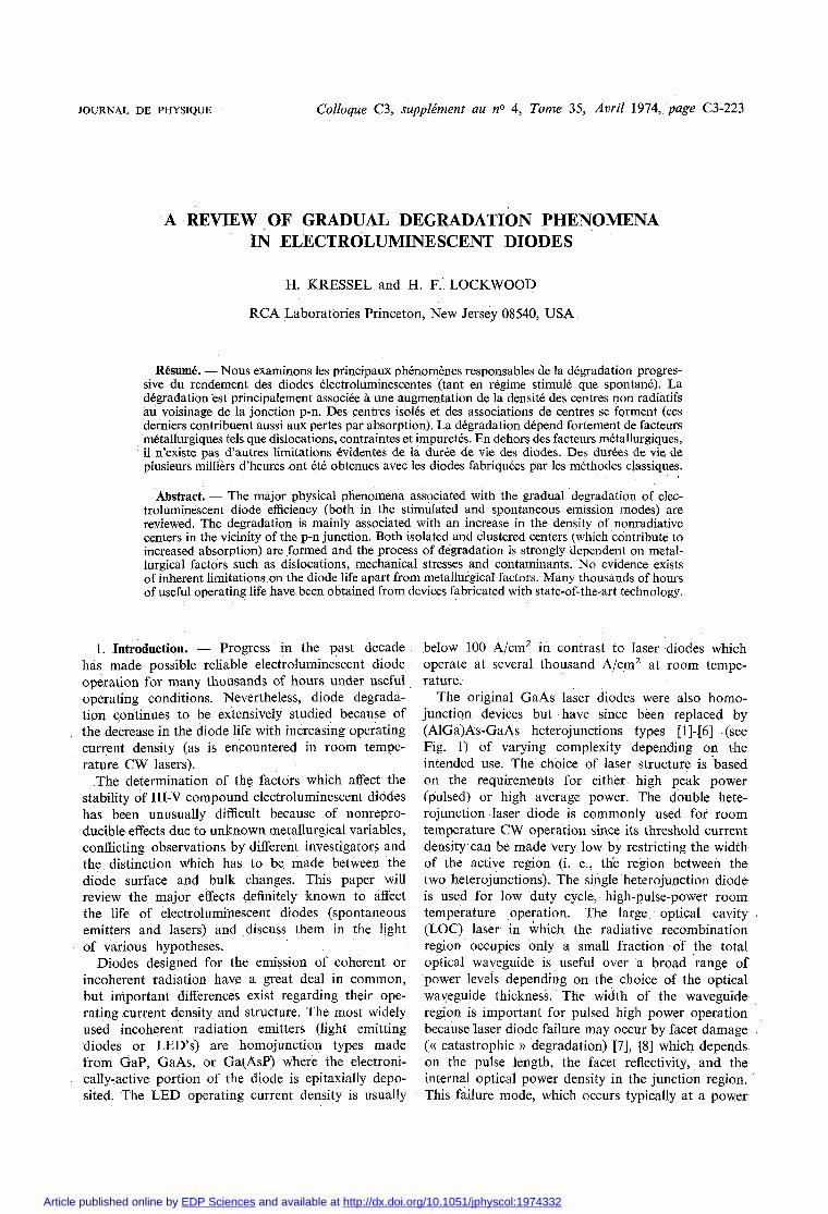
The original GaAs laser diodes were also homo- junction devices but have since been replaced by (A1Ga)As-GaAs heterojunctions types [I]-161 (see Fig. 1) of varying complexity depending on the intended use. The choice of laser structure is 'based on the requirements for either high peak power (pulsed) or high average power. The double hete- rojunction laser diode is commonly used for room temperature CW operation since its threshold current density can be made very low by restricting the width of the active region (i. e., th'e region between the two heterojunctions). The single heterojunction diode is used for low duty cycle, high-pulse-power room temperature operation. The large optical cavity (LOC) laser in which the radiative recombination region occupies only a small fraction of the total optical waveguide is useful over a broad range of power levels depending on the choice of the optical waveguide thickness. The width of the waveguide region is important for pulsed high power operation because laser diode failure may occur by facet damage ((( catastrophic )) degradation) [7], [8] which depends on the pulse length, the facet reflectivity, and the internal optical power density in the junction region. This failure mode, which occurs typically at a power
Article published online by EDP Sciences and available at http://dx.doi.org/10.1051/jphyscol:1974332

C3-224 H. KRESSEL AND H. F. LOCKWOOD
FIG. 1. - Schematic cross section of various laser structures showing the electric field distribution E in the active region, variation of the bandgap energy E, and of the refractive index n at the lasing photon energy. (a) Homojunction laser made by liquid phase epitaxy, (b) single heterojunction (( close- confined )) laser, (e) double heterojunction laser and (d) Iarge
optical cavity (LOC) laser.
level of - lo6 W/cm2, will not be discussed here. It is not the limiting factor in the reliability of room temperature CW lasers.
To simplify the presentation we briefly review the major bulk materials parameters which control the quantum efficiency of incoherent and coherent radiation. For spontaneous emission, the internal quantum efficiency qi is determined by the ratio of the radiative and nonradiative minority carrier lifetimes, z, and z,,, respectively :
rhe total minority carrier lifetime T,
is an easily measured parameter in a p-n junction while z, and z,, are difficult to determine individually.
At low injection levels, z, decreases with increasing majority carrier concentration while z,, is controlled by the density of nonradiative recombination centers. The external quantum efficiency, which is always iower than y, because of absorption within the diode bulk, can be optimized by proper design of the diode structure and ohmic contact geometry.
The basic laser diode parameters usually measured are the threshold current density, Jth, and the diffe- rential quantum efficiency, vex. Ll] :
Here, L is the distance between the cleaved facets (i. e., cavity length), R is the facet reflectivity, d is the thickness of the region of inverted population, r is the fraction of the radiation confined to the inverted population region, Po depends on the doping level in the lasing region, b ranges from 1 to 3 depending on the temperature and material, and a is the average absorption coeficient in the waveguide region.
From eq. (1)-(4), it is evident that the radiative efficiency in the spontaneous and lasing mode will be strongly affected by a decrease in q, but that in the lasing mode ?i is another important parameter. Because of the isotropic nature of the radiation in the coherent mode of operation, the absorption coefficient generally differs from a in that it represents the losses averaged over the bulk of the device, i. e., in regions well removed from the p-n junction.
It should be noted that if the density of nonradiative recombination centers is low, the internal quantum efficiency value relevant to LED operation, (eq. (I)), at low current densities may differ from that relevant to laser diode operation (eq. (3) and (4)), where the 300 K injected carrier density at threshold is about 10'' ~ m - ~ . In addition, the radiative lifetime decreases with increasing current above lasing threshold further reducing the effects of a low density of nonradiative recombination centers.
2. Diode property changes associated with gradual degradation. - A reduction in the emitted radiation from a diode operated at a constant current can be due to three basic factors : (I) increase in (( excess ))
current at the expanse of minor~ty carrier diffusion current. The excess current can increase because of higher surface leakage, an increase in generation- recombination (nonradiative) in the space charge region, or increased tunneling current due to the creation of new states in the junction ; (2) decrease of the internal radiative efficiency of the recombining minority carriers in the bulk of the diode ; (3) increase in the internal absorption.
The degradation observed in early GaAs LED'S was attributed to an increase in the surface leakage of the diode because etching of the diode periphery restored many degraded diodes [9]-[l l]. The passi- vation of the diode periphery was generally sufficient to permit many thousands of hours of stable GaAs LED operation at current densities below - 100 A/cm2.
The first conclusive evidence [12] that major changes in the bulk of the diode can occur during high current density operation (J > 1 000 A/cm2) was obtained in homojunction GaAs laser diodes prepared by liquid phase epitaxy. The degraded laser output was shown to result from an internal efficiency decrease and

A REVIEW OF GRADUAL DEGRADATION PHENOMENA IN ELECTROLUMINESCENT DIODES C3-225
increased absorption. Later results obtained using heterojunction diodes have confirmed the fact that changes within the recombination region rather than changes in the diode current components are mainly responsible for degradation. Detailed results obtained by various investigators differ, but the following observations on degradation appear to be generally valid.
1) The threshold current density of laser diodes always increases while the differential quantum efficiency frequently (but not always) [13] decreases especially in the more advanced degradation stages, as shown in figure 2.
4
DIFFERENTIAL QUANTUM
EFFICIENCY
THR~SHOLD CURRENT
DIODE CURRENT
FIG. 2. - Typical change in the power output vs diode current of a laser diode in the course of degradation. The threshold current density increases while the differential quantum efficiency
decreases.
2) The degradation rate does not depend on the optical flux density in the junction region (below the catastrophic damage point) because diodes operated at high current densities degrade similarly whether lasing or not [12]-[14]. The degradation rate is a function of the operating current density and there is evidence that it varies as the square of the current density [12]-[14]. However, because the degradation process inside the diode is usually not spatially uniform [12], the dependence of the rate on the microscopic details of electron-hole recombi- nation has not been determined.
3) There are successive degradation stages. In the early stages, when the density of nonradiative recombination centers is low, the spontaneous emission efficiency decreases without any obvious changes in the emission pattern and with only minor effects on the lasing properties. Figure 3 illustrates this behavior. Figure 3a shows the spontaneous emission decrease after 1 000 h operation as measured at relatively low current densities ; Figure 3b shows that the threshold current density increased slightly while the differential quantum efficiency of this diode in the lasing mode is unchanged. As degrada- tion proceeds, dark lines (commonly < 100 > oriented) may appear (when the emission is viewed
BEFORE
> F 4
W 0
[r
( 0 )
hrs
BEFORE J t h z 7 0 6 0 Alcrnz
X A F T E R Jth = 9 2 8 0 4 / c m 2 , / , /
- 2 3 4 5 6 7 8 9 CURRENT ( I 1
FIG. 3. - Change in the spontaneous emission efficiency and in the lasing properties of a GaAs laser diode operating at 1 000 A/cm2 for 1 OQO h dc. (a) Spontaneous emission efficiency before and after extended operation showing a significant decrease. (b) The threshold current density has increased slightly while the differential quantum efficiency is essentially unchanged. This type of behavior is illustrative of the early stages of degradation where only a relatively low density of
nonradiative centers is formed.
through the surface of the diode) in the vicinity of the ohmic contact where the current density is highest, figure 4c. These lines do not appear in the early degradation stage, as shown in figure 4b. The dark lines constitute regions of concentrated nonradiative centers and are responsible for the spotty near-field emission pattern of degraded lasers [12] and the rapid fall-off in the output of CW laser diodes at room temperature [15].
These lines form in Zn-doped diodes as well as diodes doped with other impurities ; for example, the diode shown in figure 4 was doped with Si.
4) The minority carrier lifetime decreases with the spontaneous efficiency as shown in figure 5 for Zn-doped GaAs homojunctions [16]. Assuming that the external spontaneous efficiency change follows that of yi, the change in z with yi is consistent with eq. (1) and can be attributed to a reduction in r,, (with z, remaining constant) because of the gradual formation of nonradiative recombination centers in the vicinity of the p-n junction.
Although r and J,, are also found to be related [17], a reliable correlation between the reduction in z and the increase in J,, is not possible because any

C3-226 H. KRESSEL AND H. F. LOCKWOOD
INITIAL
P = P o
0.01 cm '--I
, . ' .; h ' . . . :;:. '>>'
P = Pi15
0.02 cm I
P = Po/20
FIG. 4. - Effect of continuing operation on the surface emission from a double heterojunction diode. (a) Microphotograph of the infrared emission in the vicinity of the ohmic contact showing a clear emission pattern. (b) The diode output is reduced to 115 of the initial value Po, but no evidence of visible damage is seen. (The spots are on the surface of the diode.) (c) The diode output is reduced to 1/20 its initial value and dark lines are seen in the region of initial highest emission density. Surface
emission (A1Ga)As-GaAs : Si DH Diode ( # 517).
defects created (especially clusters or dislocations) may also increase Z [12].
5) It is a common observation that the current- voltage characteristics change as degradation proceeds. The reverse I-V characteristic <( softens >) while the excess current increases in forward bias. These I-V changes are consistent with the formation of localized defects in the junction region and a reduction in the minority carrier lifetime. However, the current- voltage measurements show no measurable change indicative of gross junction gradient changes.
6) Degradation does not require the presence of a p-n junction. Dark lines have been seen to
FIG. 5. -Data illustrating the correlation between the reduction in the diode efficiency and the reduction in the minority carrier lifetime in GaAs homojunction spontaneous emitters. The efficiency was measured at a current density of the order of 150 A/cm2. The ratio of the efficiency after degradation q to the initial efficiency qo is plotted vs the ratio of minority carrier lifetime after degradation z to the initial lifetime, T O . (After Yang,
ref. [16]).
form in heterojunction material (alln-type) optically pumped at a level either above or below lasing thresh- old [18]. Figure 6 shows ' the double heterojunction structure optically pumped, and figure 7 shows the formation of these dark regions in the most strongly excited areas. No evidence of damage was observed in the transparent (A1Ga)As window region of the structure indicating that electron-hole re~ombi- nation was necessary for degradation to occur.
7) The degradation rate at a given current density increases with temperature. But, except in special Gap and GaAs diodes contaminated with Cu (see section 3), there are as yet no extensive data for the temperature dependence of the degradation process.
8) No definitive evidence exists that degraded diodes can be recovered by annealing or other treat- ment at least at temperatures well below the melting point. While there is one report of improvement of
PUMP 6471 + 6764 - 1 0-1 5 WATTS - 104 w/crn2
(100)
1-1.5P n 5 i ~ ' ~ c r n - ~ ( 'PURE')
x-05 -
FIG. 6. - Sample geometry for optically pumped heterojunction laser. Sn and Ge were the dopants. Undoped material (all three layers -- 1015. cm-3 n-type) was also used (ref. [la]).

A REVIEW OF GRADUAL DEGRADATION PHENOMENA IN ELECTROLUMINESCENT DIODES C3-227
FIG. 7. - Degradation of p-n doped material (see Fig. 6) when operated CW by optical excitation. The material is emitting spontaneous radiation at 310 K. Top to bottom : left, t = 0, 3, 5 h ; right, with laser defocused at 3 and 5 h (ref. [IS]).
a degraded GaAs FED by reverse biasing [19], this is not a generally observed phenomenon.
3. Metallurgical factors affecting the gradual degra- dation rate. - Erratic degradation rates of diodes believed to be similarly prepared has been a common observation. The fact that some diodes are long-lived while others degrade rapidly suggests that metallurgical factors strongly influence the diode life (at least within wide limits) [12]. Systematic studies have succeeded in isolating some of the key metallurgical factors.
3.1 DISLOCATIONS - Other factors remaining constant, the degradation rate increases with dislo- cation density in GaAs, but a rather high density (2 lo4-lo5 ~ m - ~ ) is needed to affect a measurable change. Studies have been made of GaAs : Zn homo- junctions where the dislocations were introduced by
plastically deforming the substrate prior to liquid phase epitaxial growth [20]. Figure 8 shows that the diodes with high dislocation density are not signi- ficantly different initially but that they degrade at erratic rates and much more severely than the control units containing a low dislocation density. The fact that dislocations affect the diode life was also esta- blished with GaAs : Si diodes [21].
3 .2 DOPANTS. - The type of dopant and its concentration affect the diode life, but degradation is also seen in double heterojunction diodes with very lightly-doped n-type GaAs regions, and similar results have been obtained in the optically-pumped laser structure [18]. With regard to acceptors, large differences were found in homojunction diodes formed using Be as the acceptor which degraded much faster than those using Zn (a larger atom) [20]. Even with Zn-hffused junctions, however, the degradation rate

C3-228 H. KRESSEL AND H. F. LOCKWOOD
10 2 0 3 0 4 0 5 0 6 0 7 0 80 9 0 1 0 0 110 120 130 14C OPERATING T I M E (HRSI
FIG. 8. - Power emitted from GaAs homojunction laser diodes at room temperature as a function of pulsed operating time (0.04 % duty cycle, J = 1.5 x 10⁵ A/cm2) for devices as grown and plastically deformed to introduce a dislocation density of 104-105 cm-2. While the initial laser efficiency of the control and deformed diodes does not differ greatly, note the great scatter in the degradation rates of the diodes containing the high
dislocation density (ref. 1201).
depends on the details of the diffusion process [22], possibly because of reduced defect formation when the appropriate technique is used.
3.3 'MECHANICAL STRESS. - Diodes subjected to mechanical stress such as occurs by mounting with hard solders, degrade faster than unstressed diodes. Evidence for this was accumulated in early GaAs [9] LED studies.
External stress due to the mounting procedure can reduce the life by orders of magnitude as illustrated in figure 9 for CW lasers with different degrees of strain as determined from birefringence measure- ments [23].
There are also elastic strains built into heterojunction diodes due to the mismatch of lattice constant and thermal coefficient of expansion between GaAs and (A1Ga)As. The role of this factor has not been deter- mined.
3.4 CONTAMINANTS. - It is well established that the deliberate addition of Cu to GaAs and Gap diodes increases their degradation rate. In the case of Gap : Zn, 0 diodes, the efficiency reduction was due to an increase in the nonradiative tunneling current with operating time [24]. As shown in figure 10 the activation energy for the degradation process was determined to be b.53 eV from studies at various temperatures. Similar experiments with Cu in GaAs : Zn diffused homojunctions [26] yielded an activation energy for the degradation of 0.45 + 0.1 eV with
LOW MEDIUM HIGH
STRAIN
FIG. 9. -Lasing time at 300 K vs strain in CW lasers (ref. 1231).
vrrTlv
Y (CURRENT DENSITY- I O A / C ~ ~ ) I Cu CONTAMINATED
E o = 0 5 3 ev
RS TO REACH 50% DEGRADATION
PIG. 10. - Arrhenius plot of the aging results (time to reach 50 % degradation vs 1/T K) for copper contaminated Gap diodes processed in the laboratory and in a copper free envi- ronment:The Cu-contaminated divoles degrade with an acti-
vation energy of 0.53 eV (ref. [24]).
indications that the efficiency reduction was due to the internal quantum efficiency decrease rather than a simple increase in the excess current. The observed activation energy for degradation is close to the activation energy for Cu diffusion in GaAs (0.5 eV) 1261. This similarity suggests that the movement of Cu is responsible for the degradation.
4. Degradation mechanisms. - The available data suggest that the degradation is due to the formation of isolated and clustered nonradiative recombination centers and that the internal degradation process is

A REVIEW OF GRADUAL DEGRADATION PHENOMENA IN ELECTROLUMINESCENT DIODES C3-229
typically spacially nonuniform. The degradation rate is enhanced by strain and by various metallurgical defects including dislocations and 'contaminants such as Cu. Surface leakage and other sources of increased nonradiative current components which were thought to be the dominant factors in early GaAs LED work are of minor importance in explaining the degradation of diodes operated at high current densities.
The most puzzling question concerning degrada- .tion is the nature of the mechanism whereby nonra- diative recombination centers form and move at room temperature. Weisberg [27] has reviewed some possibly relevant mechanisms which we briefly discuss in the light of new data.
4.1 ENHANCED DIFFUSION IN ELECTRIC FIELDS. - Atomic diffusion could conceivably be enhanced in the electric field of the p-n junction or the very small field in the bulk of the diode (1 V/cm). However, the fact that a p-n junction is not needed for degra- dation to occur suggests that the fields play no signi- ficant role.
4.2 HIGH LOCAL TEMPERATURES - Nonuniform current distribution in forward-biased junctions could give rise to high temperatures and localized damage. There is no optical or other evidence, however, that local temperature rises of sufficient magnitude occur in the diodes studied.
4 . 3 MOTION OF INTERSTITIAL ATOMS. - L0ngini [28] suggested that the degradation of Zn-doped GaAs tunnel diodes (where junction widening occurred) could be explained by the following process. It is known that Zn can be present in both substitutional and interstitial sites on the p-side of the junction. Since the interstitial Zn ions are positit-ely charged, the reduced potential barrier at the p-n junction under forward bias allows an increased flux of these intersti- tial Zn ions into the space charge region, where they then occupied substitutional sites. Measurements of the junction capacitance which is related to the impurity gradient confirmed that Zn migration occurred.
Weisberg [27] suggested that the Longini mecha- nism could be extended to explain the degradation of Cu-doped diodes. The degradation occurs only in forward bias operation, and it is postulated that positively charged Cu ions in the p-region diffuse toward the p-n junction. With increased forward bias, the potential barrier limiting the flow Cu' into the space region is reduced. The Cu reaching the space charge region will tend to precipitate or combine with other defects because of the reduced Cu solubility in that region as directly shown by radioactive tracer studies [25]. While the above model explains the increase in tunneling currents observed in Gap [24], it does not explain the increased nonra- diative recombination seen in GaAs diodes 1251. In the absence of an external Cu source there is no
reason why the Cu concentration should increase with time in the p-region where the radiative recombi- nation occurs in GaAs : Zn homojunctions.
Finally, the Longini hypothesis is not applicable to the degradation seen in Cu-free diodes since it has been shown that degradation occurs with nonmobile dopants like Ge (unless another contaminant similar to Cu is present).
4.4 (( PHONON-KICK )) DISPLACEMENT MODEL. - In their tunnel diode studies Gold and Weisberg [29] suggested that nonradiative electron-hole recombi- nation at an impurity center could result in its dis- placement into an interstitial position leaving a vacancy behind if the displacement energy is less than the energy released in the recombination process. Simply stated, multi-phonon emission is postulated to lead to intense vibration of the recombination center which raises its effective temperature. Since the displacement energy of Zn in GaAs from a substi- tutional to an interstitial site is about 1 eV (or 0.4 eV less than the bandgap energy), this mechanism is conceivable for some impurities in the wide bandgap materials. Applying this mechanism to the degradation process, the assumption would be that the vacancy formed would have a large cross section for non- radiative recombination, and move to internal sinks.
The (( phonon-kick )> displacement process is obviously extremely improbable (especially in a homogeneous lattice), and the probability of forming a nonradiative recombination center following electron- hole recombination is therefore minute. However, it is not possible to dismiss the plausibility of this hypo- thesis on this basis alone. A simple calculation based on the observed degradation rate in GaAs homo- junction laser diodes shows that the density of centers needed to explain the observed reduction in efficiency is relatively small. For example, assuming that vacan- cies alone are formed (evidently a simplification), the probability for vacancy formation has been estimated to be as small as one displacement process for lot5 recombinations by comparing the diode degradation with the efficiency reduction due to irradiation with 1 MeV electrons [12].
The (( phonon-kick )) hypothesis explains a signi- ficant number of observations. No junctions are needed for degradation to occur. The effect of dis- locations on enhancing the degradation can be explained by the reduced displacement energy in the localized strain field in their vicinity. External stress would have a similar effect on enhancing atomic displacements and diffusion. Furthermore, the for- mation of vacancies would indeed give rise to non- radiative centers. In fact, it was shown that the nonradiative recombination centers formed in degraded Zn-doped Ga(AsP) junctions have ionization energies comparable to those formed during high energy elec- tron irradiation [30], which also reduces the diode efficiency. The model further explains the observation

C3-230 H. KRESSEL AND H. F. LOCKWOOD
that the degradation rate is a superlinear function of the current density by the fact that contiguous recombi- nation is more likely to lead to an atomic displacement than an isolated recombination event.
Unexplained by the (( phonon-kick )) hypothesis is the fact that degradation occurs even with dopants which are not as easily displaced as Zn or Cu. Fur- thermore, nonradiative recombination is assumed, while in good quality GaAs laser diodes the internal quantum efficiency above threshold approaches 100 %. The fact that degradation still occurs could be explained [I21 by assuming that the defect formation starts in flawed regions of the material where the nonradia- tive recombination probability is high to begin with and that these regions grow in size in the course of forward bias operation. Therefore, defect-free diodes will not degrade on the basis of this mechanism.
Finally, an additional modification of the cr phonon- kick n model can be suggested whereby impurities (as yet unknown) are transformed from relatively inactive forms to active nonradiative recombination centers. Eliseev [31] has used such an hypothesis to construct the kinetics of the degradation process.
5. Conclusions. - AH of the available data suggest that the hypothesis that diode degradation at high current densities is due to the introduction of non- radiative recombination centers. In more advanced stages of degradation, defect clusters form (possibly at dislocation sites) which strongly affect laser diode properties including increase in the absorption coeffi- cient [32]. There is evidence that the nonradiative centers are formed by atomic displacements, but the
microscopic dynamics are still uncertain, although the (( phonon-kick )) hypothesis does explain a number of observations in devices operating at high current densities.
The degradation rate depends on many metallur- gical factors for a given current density. Copper has definitely been found to be detrimental, in Gap and GaAs, but Cu can be effectively removed by various leaching techniques. For this reason it is not believed that Cu is a significant factor in controlling, the operating life of devices made by liquid phase epitaxy. However, other contaminants, so far uniden- tified, may be relevant.
Dislocations and outside mechanical stresses are also detrimental. Both of these factors can be elimi- nated by careful material preparation and assembly. However, some strain is inevitably built into hetero- junction diodes which could limit the ultimate life of such diodes operated at high current densities. At this time, results in various laboratories indicate that room temperature CW laser diode life in excess of 1 000 h is possibly with selected diodes. Incoherent emitters operating below 1 000 A/cm2 have demons- trated lifetimes of many thousands of hours. There is no evidence so far that an inherent limit exists to electroluminescent diode life apart from factors associated with metallurgical flaws.
Note added in prooj - PETROFP, P. and HARTMAN, R. L. [Appl. Phys. Lett. 23 (1973) 4691 have used transmission elec- tron microscopy to show that three dimensional dislocation networks can nucleate at existing dislocations during double heterojunction operation as a result of a climb mechanism which requires vacancies.
References
[I] For a review see KRESSEL, H., in Laser Handbook, F. T . Arecchi and E. 0. Schulz-DuBois, eds. (North Holland Pub. Co., Amsterdam) 1972.
[2] KRESSEL, H. and NELSON, H., RCA Review 30 (1969) 106. [3] LOCKWOOD, H. F., KRESSEL, H., SOMMERS, H. S., Jr. and
HAWRYLO, F. Z., Appl. Phys. Lett. 17 (1970) 499. [4] KRESSEL, H., LOCKWOOD, H. F., and HAWRYLO, F. Z.,
J. Appl. Phys. 42 (1972) 561. [5] ALFEROV, Zh. I., ANDREEV, V. M., PORTNOI, E. I. and
TRUKHAN, M. K., SOV. Phys. Seinicond. 3 (1970) 1107.
[6] HAYASHI, I., PANISH, M. B., FOY, P. W. and SUMSKI, S., Appl. Phys. Lett. 17 (1970) 109.
[7] KRESSEL, H. and MIEROP, H., J. Appl. Phys. 38 (1967) 5419.
[8] ETTENBERG, M., SOMMERS, H. S., Jr., KRESSEL, H. and LOCKWOOD, H. F., Appl. Phys. Lett. 12 (1971) 571.
[9] B~ARD, J. R., PITTMAN, G. E. and LEEZER, J. F., P~oc. k t . Symposium on GaAs, Reading, Inst. Phys. and the Phys. Soc., London (1967), p. 113.
[lo] LAMORTE, M. F. et al., Proc. Int. Symposium on GaAs, Reading, Inst. Phys. and the Phys. Soc., London (1967), p. 118.
[ l l ] JACOBUS, W. N., Solid-State Electron. 10 (1967) 260. [12] KRESSEL, H. and BYER, N. E., Proc. ZEEE 38 (1969) 25.
[13] NEWMAN, D. H., RITCHIE, S. and O'HARA, S., IEEE J. Quantum Electron. QE-8 (1972) 379.
1141 BYER, N. E., IEEE J. Quantum Electron. QE-5 (1969) 242.
[I51 DELOACH, B. C., Jr., HAKKI, B. W., HARTMAN, R. L. and D'ASARO, L. A., Proc. ZEEE, July 1973.
[16] YANG, E. S., ZEEE J. Quantum Electron. QE-7 (1971) 239. For some earlier results dealing with the decrease in z see
SUSHKOV, V. P. and SHCHEPETILOVA, L. A., SOV. Phys.- Semicond. 4 (1970) 967.
[17] YANG, E. S., J. Appl. Phys. 42 (1971) 5634. [18] JOHNSTON, W. D. and MILLER, B. I., Appl. Phys Lett.
23 (1973) 192. [19] BURRUS, C. A. and DAWSON, R. W., Appl. Phys. Lett.
17 (1970) 97. [20] KRESSEL, H., BYER, N. E., LOCKWOOD, H. F., HAWRYLO,
F. Z., NELSON, H., ABRAHAMS, M. S. and MCFARLANE, S. H., Met. Trans. 1 (1970) 635.
[21] METTLER, K. and PAWLIK, D., Siemens Forsch. u. Entwickl. 1 (1972) 274.
[22] KONNERTH, K. L., MARINACE, J. C. and TOPALIAN, J. C., J. Appl. Phys. 41 (1970) 2060.
[23] HARTMAN, R. L. and HARTMAN, A. R., Appl. Phys. Lett. 23 (1973) 147.

A REVIEW OF GRADUAL DEGRADATION PHENOMENA IN ELECTROLUMINESCENT DIODES C3-231
[24] BERGH, A. A., Proc. 8th Annual Reliability Physics Confe- rence (IEEE Catalog 70 C 59-PHY), p. 48 (1970).
[25] BAHRAMAN, A. and OLDHAM, W. G., J. Appl. Phys. 43 (1972) 2383.
[26] HALL, R. N. and RACETTE, J. H., J. Appl. Phys. 35 (1964) 379.
[27] WEISBERG, L. R., in reference [24], p. 43. [28] LONGINI, R. L., Solid-State Electron. 5 (1967) 177. [29] GOLD, R. D. and WEISBERG, L. R., Solid-State Electron. 7
(1964) 811.
[30] SCHADE, H., NUESE, C. J. and GANNON, J. J., J. Appl. Phys. 42 (1971) 5072. The traps are located at 0.2 and 0.4 eV from either edge. The estimated density of centers formed is 5 x 10¹⁴ to 6 x 1015 cm-3 with corresponding reductions in the GaAso 6P0.4 diode efficiencies of - 15 % and - 50 % at a current density of 10 A/cmz.
[31] ELISEEV, P. G., SOV. Phys.-Semicond. 6 (1973) 1431. 1321 HAKKI, B. W. and PAOLI, T. L., J. Appl. Phys. 44 (1973)
4113.
DISCUSSION
A. VECHT. - What is the effect of temperature on the degradation process and does this gives a clue to mechanism ?
H. KRESSEL. - In general, the degradation rate increases with temperature. This effect is particularly marked in diodes containing contaminants, such as Cu. In other diodes, the degradation dependence on temperature has not been studied well enough to pro- vide significant clues.
Y. MARFAING. - Pour un laser fonctionnant (( temptrature ambiante D, quelle est en .fait la temp6 rature de la zone active ?
H. KRESSEL. - The actual temperature of the active region can be estimated from the shift of the emission spectra with increasing current. Typically, the CW diodes are operated close to threshold and the tempe- rature rise is under 30 OC above the heat sink tem- perature.
C. BENOIT A LA GUILLAUME. - Le rtgime en impul- sions est-il plus efficade que le rtgime continu pour la dtgradation des lasers ?
H. KRESSEL. - Non.