a self-testing and calibration method for embedded ... · a self-testing and calibration method for...
TRANSCRIPT

A Self-Testing and Calibration
Method for Embedded Successive
Approximation Register ADC
ASPDAC 2011
X.-L. Huang*+, P.-Y. Kang*, H.-M. Chang#, J.-L. Huang*,
Y.-F. Chou+, Y.-P. Lee+, D.-M. Kwai+, and C.-W. Wu+
* National Taiwan University, Taiwan
+ Industrial Technology Research Institute, Taiwan
# University of California, Santa Barbara, USA
1
Outline
Introduction
Preliminaries
The proposed Technique
Simulation Results
Conclusion
2

Introduction
The successive approximation register (SAR)
ADC is widely used in modern mixed-signal
SOC designs
High power efficiency and low area overhead
Component mismatch limits its performance
ADC testing in SOC design is difficult
Requires high quality test stimulus
Lengthy testing
I/O accessibility is limited
3

Previous Works
Testing [Goyal, ITC 2005] Selective code testing to reduce test time
Incapable of handling missing code issue
The required test ramp is impractical for on-chip generation
Calibration [Liu, ISSCC 2009] Employs a slow but accurate reference ADC and LMS technique
to perform background calibration
The reference ADC usually incurs significant area overhead
The LMS algorithm demands intensive computation and lengthy
calibration time
4

The Proposed Technique
This paper presents a self-testing and
calibration technique for embedded SAR ADC Test the SAR ADC by measuring the major carrier transitions
(MCTs) of its DAC capacitor array
Calibrate the SAR ADC by eliminating all the missing codes
digitally
The MCTs of the DAC capacitor array are
directly generated and measured by The comparator in the SAR ADC
An additional DfT DAC (d-DAC)
5

The Advantages and Contributions
The ideal MCT voltage is just 1 LSB
The required analog measurement range is small
Simplifies the d-DAC implementation
The control signals and test responses are all-
digital
One can reuse the on-chip digital resources for test
result analysis and missing code calibration
This further reduces the incurred design and area
overhead
6

Outline
Introduction
Preliminaries
The proposed Technique
Simulation Results
Conclusion
7

Basic SAR ADC Structure
The SAR ADC is consisted of
Binary-weighted DAC capacitor array
Comparator
SAR Control logic
02 CC i
i
0CCr

Conversion 1: Sample Mode
Sample the input voltage into the capacitors

Conversion 2: Hold Mode
Sg open, and all the top plates are connected
to ground
inX VV

Conversion 3: Redistribution Mode (1/2)
Iterative binary search process (from MSB to LSB)
First, the top plate of C3 is connected to Vref
refinref
total
inX VVVC
CVV
2
13

Conversion 3: Redistribution Mode (2/2)
Vx is then compared to ground
Vx > 0, D3=0 and the top plate of C3 will reconnect to ground
Vx < 0, D3=1
After D3 is resolved, the process moves down to next bit.
N iterations is required for N-bit ADC
Let CH(i) denote the capacitance connected to Vref ,
Vx in i-th iteration can be expressed as
ref
total
HinX V
C
iCVV
)(

DAC MCT Testing (1/3)
SAR ADC linearity can be characterized by measuring
the major carrier transitions (MCTs) of the DAC
The code transition level (VT) of
For the ADC code in the form of 2i-1, the code width is
011 DDDN
ref
total
N
i ii
NT VC
CDDDDV
1
0011 )(
ref
total
i
j jii
T
i
T
i
CW VC
CCVVV
1
0)12()2()12(

DAC MCT Testing(2/3)
All the code widths can be
expressed by
is also known as the
major carrier transition of the
DAC
Many code transitions share
the same capacitor switching
activities
Binary Decimal
0000 0
0001 1
0010 2
0011 3
0100 4
0101 5
0110 6
0111 7
1000 8
1001 9
1010 10
1011 11
1100 12
1101 13
1110 14
1111 15
S1S2
S3
S4
)12( i
CWV
)12( i
CWV

DAC MCT Testing (3/3)
S1
0000 0
0001 1
0010 2
0011 3
0100 4
0101 5
0110 6
0111 7
1000 8
1001 9
1010 10
1011 11
1100 12
1101 13
1110 14
1111 15
S2
0000 0
0001 1
0010 2
0011 3
0100 4
0101 5
0110 6
0111 7
1000 8
1001 9
1010 10
1011 11
1100 12
1101 13
1110 14
1111 15
S3
0000 0
0001 1
0010 2
0011 3
0100 4
0101 5
0110 6
0111 7
1000 8
1001 9
1010 10
1011 11
1100 12
1101 13
1110 14
1111 15

Errors in SAR ADC
Comparator offset
Causes global shift to the transfer curve
Can be compensated by auto-zeroing techniques
Capacitor mismatch
Affect the code widthref
total
i
j jii
CW VC
CCV
1
0)12(
Vin
Outp
ut
Code
missing decision level
Ideal Transfer Curve
0
1
2
3
4
5
6
7
Vin
Outp
ut
Code
missing transition level
Ideal Transfer Curve
0
1
2
3
4
5
6
7

Outline
Introduction
Preliminaries
The proposed Technique
Simulation Results
Conclusion
17

The Proposed DfT Architecture
18
MCT Generation
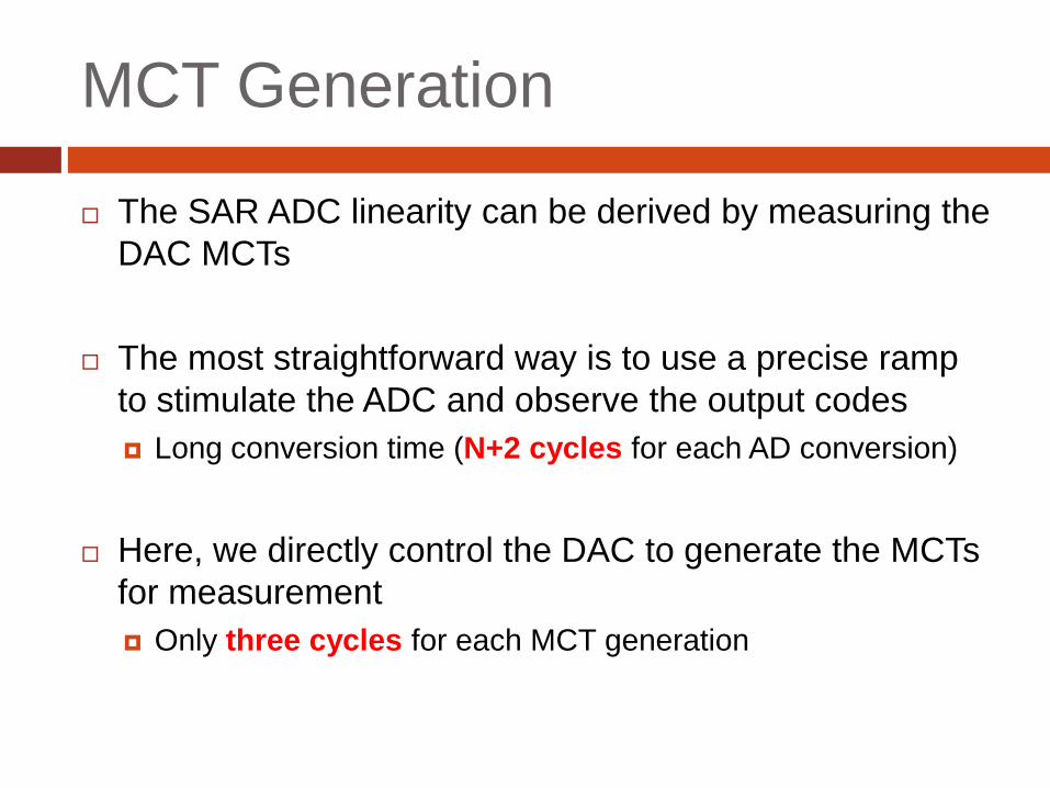
The SAR ADC linearity can be derived by measuring the
DAC MCTs
The most straightforward way is to use a precise ramp
to stimulate the ADC and observe the output codes
Long conversion time (N+2 cycles for each AD conversion)
Here, we directly control the DAC to generate the MCTs
for measurement
Only three cycles for each MCT generation

MCT Generation: 0111->1000 (1/3)
Connect the top plates of LSB capacitors to Vref

MCT Generation: 0111->1000 (2/3)
Sg open, and all the top plates are connected
to ground
ref
total
j j
TX VC
CVV
2
0)0111(

MCT Generation: 0111->1000 (3/3)
The top plate of C3 is connected to Vref
ref
total
j j
TTCWX VC
CCVVVV
2
03
)0111()1000()0111(

MCT Characterization
MCTs are measured by a short linear ramp
together with the internal comparator
The test ramp is generated by d-DAC
FSR is 4 LSBs of the ADC
The resolution is 6-bit

The Testing Flow
24
Start
Set mi=0
Next bit i ?
Force the DAC capacitor
array to generate
VT(2i) - VT(2i-1-mi)
VT(2i) < VT(2i-1-mi) ?
mi=mi+1
Measure VCW(2i-1-mi)
and record mi
Construct the ADC I/O
transfer curve
Quantization error
removal
DNL/INL Analysis
End
No
Yes
No
Yes
Comparator Offset
Measurement

Quantization Error Removal
Calculate the difference between the actual
ADC FSR and its ideal value, and linearly scale
back this difference to all the existing codes
code
idealest
n
FSRFSR
0)( if ,)()'( iViViV CWCWCW

Missing Code Calibration
Compensation codes are computed according
to mi’s.
The calibrated code is obtained by subtracting
the compensation code from the raw code.
Analog Input
Outp
ut
Code
/ D
N-1
DN
-2
mN-2
(a)
mN-1
mN-2
Analog Input
Outp
ut
Code
mN-1+2mN-2
(b)
mN-2
mN-1+mN-2
00
01
10
11
00 if,
01 if ,
10 if ,
11 if ,
0
2
21
21
21
21
2
21
21
n-n-
n-n-
n-n-
n-n-
N
NN
NN
cmp
DD
DD
DD
DD
m
mm
mm
C

Outline
Introduction
Preliminaries
The proposed Technique
Simulation Results
Conclusion
27

Simulation Setup
10-bit SAR ADC with conversion radix set to 1.95
Capacitor mismatch is set within 5%
Comparator offset is set within 1 LSB
A 6-bit DAC is designed for test stimulus generation
The FSR is only 4 LSBs of the ADC
2 LSBs for analog measurement and 2 LSBs for offset tolerance
Noise on the signal path is Gaussian with 0.1 LSB
standard deviation
28

Testing Results
Histogram testing results
Noise free
Average code hit is 16
The required test cycles
is about 160K
DNL/INL: -1/-16.53 LSB
The proposed technique
Gaussian noise with 0.1
LSB standard deviation
Each MCT is sampled 10
times
The required test cycles is
about 0.5K
DNL/INL: -1/-16.53 LSB
Test errors are all less than 0.1 LSB29

Calibration Results
Before Calibration DNL/INL: -1/-16.53 LSB
After Calibration DNL/INL: -0.42/-0.57 LSB
All of the missing codes are eliminated
30

Massive Simulation
The proposed technique is applied to 1000 SAR ADCs
The DNL/INL test errors are all within 0.1/0.3 LSB
The average DNL/INL are improved from 1/16.75 LSB to
0.61/0.48 LSB
31

Outline
Introduction
Preliminaries
The proposed Technique
Simulation Results
Conclusion
32

Conclusion
This paper presents a simple yet efficient
technique for testing and calibrating the
embedded SAR ADC
Simulation results validate the effectiveness and
robustness of the proposed technique
A prototype is currently being designed for
further silicon validation
33