a single-poly eeprom cell for embedded memory applications€¦ · in this paper, we describe the...
TRANSCRIPT

1
A Single-Poly EEPROM Cell for Embedded Memory Applications
A. Di Bartolomeo1,2,*
, H. Rücker1, P. Schley
1, A. Fox
1, S. Lischke
1, Kee-Yeol Na
1,3
1 IHP Microelectronics, Im Technologiepark 25, 15236 Frankfurt (Oder), Germany
2 Dipartimento di Fisica E.R. Caianiello and INFN Gruppo Collegato di Salerno and Centro
Interdipartimentale di Ricerca NANO_MATES, Universitá di Salerno, via S. Allende, 84081,
Baronissi, Italy
3 Chungbuk Provincial College, Okcheon Eup, Okcheon Goon, Chungbuk, Korea, 373-807
Abstract
We present a novel single poly-silicon EEPROM cell for embedded memory. The cell is
integrated in a 0.13 �m RF-CMOS technology without process modifications and is
composed of an NMOS transistor and a MOS capacitor on two isolated P-wells sharing a
floating poly-silicon layer. A two-polarity voltage of ± 6 V is applied for writing and erasing
using uniform channel Fowler-Nordheim tunnelling. Operations faster than 1 ms, endurance
over 10+3
cycles and data retention longer than 10 years are demonstrated.
Keywords: non-volatile memory, Flash memory, EEPROM, single-polysilicon, Fowler-
Nordheim tunnelling, reliability, endurance, data retention.
1. Introduction
The continuous enhancement of performance and functionality in virtually all electronic
systems has raised the demand for embedded non-volatile memories (NVM) for permanent
but upgradeable storage of configuration and personalization data and/or operating and
application codes. Many system-on-chip (SoC) applications in the consumer and
communication areas require moderate amounts of NVM of a few kbit and a limited number
of write and erase operations to integrate functions such as security code encryption or tuning
of analog circuits.
In the past decade, several research efforts have been addressed toward new embedded non-
volatile cells which facilitate integration into existing CMOS or BiCMOS technologies. In
this context, single poly-silicon non-volatile devices have attracted considerable attention [1-
8].
* Corresponding author. E-mail address: [email protected]

2
In the present work, we report on a novel single-polysilicon EEPROM (SPEE) cell concept
that utilizes uniform-channel Fowler-Nordheim (FN) tunnelling for programming and erasing.
The SPEE cells were fabricated in a 0.13 µm RF-CMOS/BiCMOS process [9] without any
process modification. This process offers also high-speed SiGe heterojunction bipolar
transistors. However, only standard features of the RF-CMOS process were used for the
integration of SPEE cells discussed here. The memory cells, constituted by an NMOS
transistor and a MOS capacitor, is built on two isolated P-wells, capacitively connected by a
common poly-silicon layer functioning as floating gate.
The choice of a single polysilicon cell was driven by the possibility of integration without
additional masks or extra process steps. Further requirements were the limitation of the
maximum voltages for write and erase operations to values well below breakdown of
source/drain junctions and the request of low power consumption for wireless applications.
Taking advantage of the isolated P-well available in the triple-well process, the design of the
SPEE cell enables two-polarity voltage for write/erase operations and avoids high voltage
sources and signals. Its structure has been conceived for twofold uniform-channel Fowler-
Nordheim (FN) programming which limits power consumption.
In this paper, we describe the structure of the SPEE cell and discuss data relevant to write and
erase operations, endurance and data retention. Based on the results achieved, we consider the
cell as a promising device for embedded memory applications with a size of a few kbit and
about one thousand write/erase cycles.
2. Cell structure
The SPEE cells are fabricated in a 0.13 µm RF CMOS process without process changes. The
process offers a 2.0 nm and a 7.0 nm gate oxide for 1.2 V and 3.3 V CMOS devices,
respectively. A deep N-well is available for the fabrication of isolated NMOS devices. In the
SPEE cells, the 7.0 nm gate oxide is used as the tunnel oxide. The deep N-well of the CMOS
process is also used for the isolation of the non-volatile memory cells.
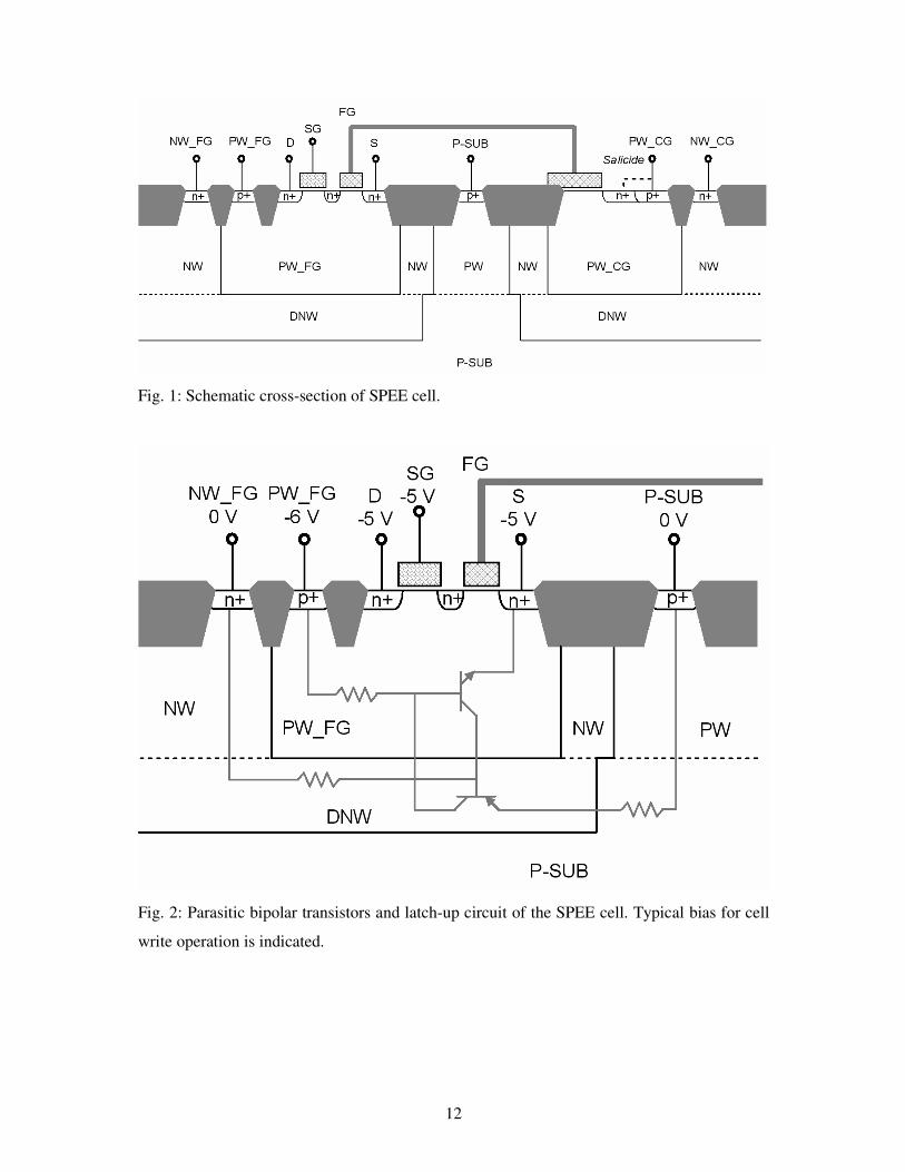
The cross section of the SPEE cell is shown in Fig. 1. The cell consists of an NMOS transistor
(FG-MOS) and a MOS capacitor (MOS-C) with a shared poly-silicon layer, which serves
both as gate of the FG-MOS and as top plate of the MOS-C. This poly-silicon layer (n-type) is
electrically floating and constitutes the charge trapping element, i.e. the floating gate (FG) of
the cell. The control gate (CG) is made by an isolated P-well (PW_CG). A second isolated p-
well (PW_FG) is housing the FG-MOS. A select NMOS transistor (SG-MOS), in series with
the FG-MOS and in the same P-well, has been added to have additional control on the cell

3
operations and to avoid overerase failures in memory arrays. The proposed SPEE cell uses an
isolation scheme that allows one to bias the control gate and the well of the FG transistor with
two polarities. This scheme facilitates the use of Fowler-Nordheim tunnelling for write and
erase operations.
The MOS capacitor (as well as the FG-MOS one on the other well) is operated either in
accumulation or in inversion for write and erase operations, respectively. An n+ diffusion,
shorted to the p+ contact of the PW_CG by a common salicide layer, serves as electron
reservoir for the fast formation of the inversion layer at the surface of the PW_CG.
For a programming time of 1 ms or less and the given thickness of the tunnel gate oxide of 7
nm, the voltage across the oxide has to be higher than 10 V which is close to the breakdown
voltage of the S/D-well junctions. This problem is overcome by halving the voltage and
applying simultaneously positive and negative pulses to the control and floating gate wells,
which receive biases always safely below their breakdown. In such conditions, uniform
channel electron Fowler-Nordheim (FN) tunnelling takes place between the PW_FG and the
floating poly-silicon layer on top of it [10]. Compared to other schemes, the twofold FN
mechanism has the advantage of lower power consumption and simpler source/drain layout.
The lower voltage between source and P-well during erase operation results in the absence of
band-to-band tunnelling which is favourable for the cell reliability. The non-complex
source/drain engineering on the other hand enables simpler process integration, lower area
consumption and easier scaling to smaller dimensions.
SPEE cells with different lengths of the FG_MOS gate and different areas of the MOS
capacitor have been manufactured. In the present work, we focus on the characterization of
cells which have FG_MOS with L/W = 0.33 �m/0.15 �m and MOS_C with active area of
0.3×5.335 �m2. Similar results were obtained for cells with scaled FG_MOS transistors with
L/W = 0.24 �m/0.15 �m. The dimensions of the MOS-C have been chosen to have a high
coupling ratio, which obviously results in faster writing and erasing [5,11].
3. SPEE characterization
3.1. Write/erase operations
Typical bias voltages applied to SPEE cells for erase and write operations and for Vt
measurement are listed in Table 1. In this paper, we designate as written the status with
electrons stored in the floating gate, i.e. the status with higher threshold voltage, Vt. The Vt is
defined as the control gate voltage, VPW_CG, at which the drain current IDS is equal to 45 nA,
i.e. to (100 × W/L) nA, when VDS = 0.1 V and VSG = 3.3 V.

4
The voltages applied to PW_CG and PW_FG terminals determine all the other biases and
therefore the electric field across the tunnel oxide. These voltages have opposite sign but
usually the same absolute value, which is referred as programming voltage below. More
specifically, cell writing (erasing) is achieved by applying a positive (negative) voltage to
PW_CG and a negative (positive) one to PW_FG, while electrons are injected into (ejected
from) the floating gate. NW_FG and NW_CG terminals are biased to keep the junction with
the respective P-well reverse biased. The simultaneous biasing of source (S), drain (D) and
select gate (SG) terminals is needed to provide electrons for the fast formation of an inversion
layer at the surface of the PW_FG below the floating gate for uniform-channel FN tunnelling
and to avoid unwanted leakage current to the SG gate. It can be noticed that S, D, and SG
terminals are kept at a common potential, systematically 1 V higher than the bias applied to
PW_FG. This potential defines the potential of the inversion channel of the FG_MOS, thus
determining the effective negative potential during writing. The higher voltage at the S, D,
and SG terminals was introduced to eliminate any risk of latch-up.
Latch-up due to the parasitic bipolar transistors formed by the nested wells (Fig. 2) could
occur if the junction between PW_FG and S/D is forward biased. Such an event could happen
when applying the positive pulse to the PW_CG because of the high resistance of PW_FG. In
the cells investigated here, the contact to the PW_FG and the FG_MOS are located in
different active regions separated by a shallow trench (Fig. 2). This results in a high resistance
of the FG_PW due to a sheet-resistance of about 5 k�/sq. of the isolated P-well below the
shallow trench. The problem of the high resistance of the PW_FG and thus the risk of latch-up
can be avoided by contacting the P-well within the active area of the FG_MOS in a new
layout. In the present investigation, we have excluded any risk of latch-up by applying at S
and D a potential that is 1V above the potential of the PW_FG.
Fig. 3 shows the transfer characteristics of the FG-MOS for a SPEE cell as produced, after
write and after erase. The negative value (- 0.4 V) of the threshold voltage of the as-produced
cell is due to the positive bias applied during Vt measurement to NW_CG, which has a
capacitive coupling to floating gate that can invert the surface of PW_FG. The programming
operations shift the transfer curve and increase the Vt. The more negative Vt after erase
means that the floating gate has now a net positive charge which transforms the FG-MOS
transistor from an enhancement to a depletion device.
The transient characteristics of the SPEE cell are shown in Fig. 4 (a) and (b). They are
obtained by applying successive voltage pulses of growing length (for pulse heights of ± 5.5
V, ± 6.0 V and ± 6.5 V, respectively). Fig. 4 (a) shows that a threshold voltage Vt = + 2 V (Vt
5
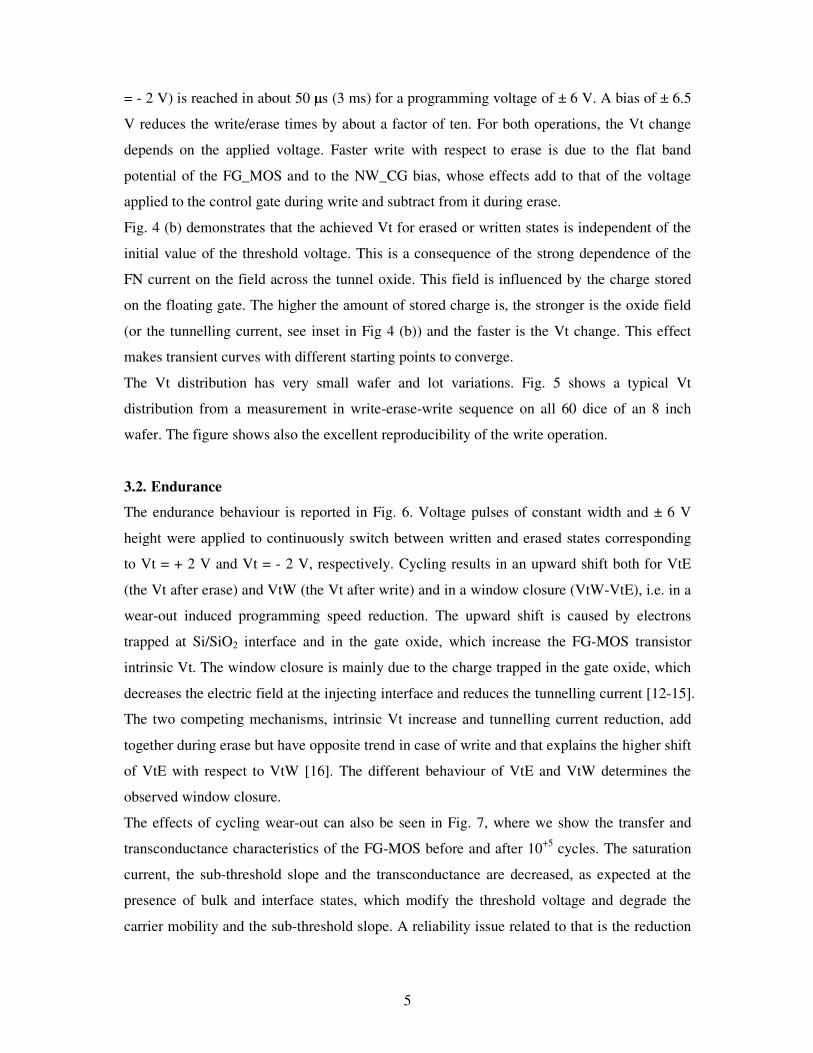
= - 2 V) is reached in about 50 �s (3 ms) for a programming voltage of ± 6 V. A bias of ± 6.5
V reduces the write/erase times by about a factor of ten. For both operations, the Vt change
depends on the applied voltage. Faster write with respect to erase is due to the flat band
potential of the FG_MOS and to the NW_CG bias, whose effects add to that of the voltage
applied to the control gate during write and subtract from it during erase.
Fig. 4 (b) demonstrates that the achieved Vt for erased or written states is independent of the
initial value of the threshold voltage. This is a consequence of the strong dependence of the
FN current on the field across the tunnel oxide. This field is influenced by the charge stored
on the floating gate. The higher the amount of stored charge is, the stronger is the oxide field
(or the tunnelling current, see inset in Fig 4 (b)) and the faster is the Vt change. This effect
makes transient curves with different starting points to converge.
The Vt distribution has very small wafer and lot variations. Fig. 5 shows a typical Vt
distribution from a measurement in write-erase-write sequence on all 60 dice of an 8 inch
wafer. The figure shows also the excellent reproducibility of the write operation.
3.2. Endurance
The endurance behaviour is reported in Fig. 6. Voltage pulses of constant width and ± 6 V
height were applied to continuously switch between written and erased states corresponding
to Vt = + 2 V and Vt = - 2 V, respectively. Cycling results in an upward shift both for VtE
(the Vt after erase) and VtW (the Vt after write) and in a window closure (VtW-VtE), i.e. in a
wear-out induced programming speed reduction. The upward shift is caused by electrons
trapped at Si/SiO2 interface and in the gate oxide, which increase the FG-MOS transistor
intrinsic Vt. The window closure is mainly due to the charge trapped in the gate oxide, which
decreases the electric field at the injecting interface and reduces the tunnelling current [12-15].
The two competing mechanisms, intrinsic Vt increase and tunnelling current reduction, add
together during erase but have opposite trend in case of write and that explains the higher shift
of VtE with respect to VtW [16]. The different behaviour of VtE and VtW determines the
observed window closure.
The effects of cycling wear-out can also be seen in Fig. 7, where we show the transfer and
transconductance characteristics of the FG-MOS before and after 10+5
cycles. The saturation
current, the sub-threshold slope and the transconductance are decreased, as expected at the
presence of bulk and interface states, which modify the threshold voltage and degrade the
carrier mobility and the sub-threshold slope. A reliability issue related to that is the reduction
6
of the read current and the increase of the drain leakage which have to be taken into account
in the design of memory blocks.
Endurance tests on CAST arrays [17] of 1024 cells in-parallel show the same behaviour with
similar upward Vt shift and window closure (Fig. 8). By analogy to the single cell, the
threshold voltage of the array is determined as the PW_CG potential which gives a current of
1024×45 nA for VDS = 0.1 V and VSG = 3.3 V.
It is also important to notice that the endurance characteristics are not worsened by an
enlarged programming window. Furthermore, we did not experience the initial decrease of the
erased Vt, sometimes observed on Flash endurance tests as a consequence of hole generation
and trapping, whose positive charge enhances the tunnelling efficiency.
A high temperature baking at more than 100 °C is expected to deactivate some of the defects
created during cycling and re-establish the electrical behaviour of the cells. Fig. 9 confirms
this expectation showing the effect of a ~200 hours bake at 250 °C on cells previously
subjected to 10+4
write/erase cycles. Apart from the charge loss (see next paragraph), the
improvement of the sub-threshold and transconductance characteristics is evident confirming
the deactivation of cycling induced defects at Si/SO2 interface.
Many applications of embedded memories require a limited number of write/erase cycles,
typically below 10+3
during the lifetime of the circuit. Accordingly, the endurance
specifications can be conservatively limited to 10+3
cycles. A variation of less than 1 V in VtE
and VtW and a Vt window closure of less than 20 % is measured after 10+3
cycles.
3.3. Data retention
Data retention has been studied by programming all 60 cells of an 8 inch wafer to Vt = + 4 V
and measuring the threshold voltage and the transfer characteristics at regular intervals during
a multi-hour bake at 250 °C. At such conditions, charge loss is accelerated by temperature and
field, which increase thermionic emission over the Si-SiO2 barrier, field-assisted electron
injection, electron detrapping and transport through the oxide.
Fig. 10 shows the time evolution of Vt during the test. It also shows the threshold voltage of a
sample of cells from a different wafer programmed to Vt = 6 V and stored at room
temperature. As expected, charge loss is faster for combined effect of temperature and field.
Fig. 10 shows a decreasing average Vt with a broadening distribution. Nevertheless, we point
out that all the cells remain in the same distribution, meaning that there are no devices with
anomalous oxide leakage in the studied samples.

7
Since data retention tests need statistics of a high number of cells to detect anomalous bits, the
same test was performed on 1 kbit CAST arrays. The threshold voltage for the array is here
defined at the same current level as the Vt of the single cell (i.e. at 45 nA, a current
corresponding to deep sub-threshold region), thus allowing the detection of cells with
anomalous leakage current as a down-shift of VtE [17]. The failure of 2 arrays out of 60 is
shown in Fig. 11, where two arrays are subjected to significant charge loss during the first few
hours. One failing array shows an immediate Vt reduction, that stops around 2V, with the
array afterwards following the main distribution. Such behaviour is attributed to so-called stop
bits, i.e. defective bits that are suddenly transformed to normal cells for leakage path
annealing during retention baking [18]. The second failing array reaches the non-written
status very soon, indicating the presence of one or more leaky cells, likely due to some
extrinsic defects that may induce conductive paths in the oxide.
Fig. 10 and 11 show also data for retention after cycling. Despite the poor statistics, the
collected data show that retention, in average, is not affected by 10+4
write/erase cycles.
The temperature dependence of the data retention is described by the Arrhenius model (teq =
texp·exp[Ea/kb·(1/Teq - 1/Texp)] where teq/exp and Teq/exp are the equivalent/experimental time and
temperature, Ea conservatively assumed to be 0.6 eV is the activation energy and kb is the
Boltzmann constant [19, 20]). Using this relation, our data can easily be converted to the more
conventional temperature of 55 °C used for Flash memory endurance specifications [21] thus
covering a time interval of 116 years. In particular, by assuming a starting Vt of 2 V, an
average Vt reduction less than 20 % is expected after 10 years at 55 °C (see inset in Fig. 10).
4. Conclusions
We have presented the design and electrical characterization of a novel single-poly EEPROM
cell that constitutes a promising device for embedded memory applications with medium size
of a few kbit and about one thousand write/erase cycles. The cell, manufactured in a 0.13 �m
RF CMOS technology without process changes, is composed of an NMOS transistor and a
MOS capacitor on two isolated P-wells, topped by a poly-silicon layer serving as floating gate.
The maximum required voltage for programming operations can be restricted to ± 6 V by
using dual-polarity voltages. Write and erase are performed by uniform channel FN tunnelling,
with endurance of more than 10+3
cycles and charge retention longer than 10 years at 55 °C.

8
References
[1] Ohsaki K, Asamoto N, Takagaki S. A Single Poly EEPROM Cell Structure for Use in
Standard CMOS Processes. IEEE Journal of Solid State Circuits 1994;29;3:311-316.
[2] Baldi L, Cascella A, Vajana B. A scalable single poly EEPROM cell for embedded
memory applications. Microelectronic Journal 1997;28:657-661.
[3] McPartland R J, Singh R. 1.25V, Low-Cost, Embedded FLASH Memory for Low-Density
Applications, Symposium on VLSI Circuits, Digest of Technical Paper 2000:158-161.
[4] Carman E, Parris P, Chaffai H, Cotdeloup F, Debortoii S, Hemon E, Lin-Kwang J, Perat O,
Sicard T. Single poly EEPROM for Smart Power IC´s. Proceedings of The 12th International
Symposium on Power Semiconductor Devices and ICs 2000:177-179.
[5] Shalchian M, Atarodi S M. A Logic CMOS Compatible Flash EEPROM for Small Scale
Integration. Proceedings of the 15th International Conference on Microelectronics, ICM2003,
2003:348-351.
[6] Vega-Castillo P, Krautschneider W, Single poly PMOS-based CMOS compatible low
voltage OTP, Proceedings of SPIE, the International Society for Optical Engineering, VLSI
circuits and systems. Conference No2. 2005;5837:953-960.
[7] Ren T, Pan L, Liu Z, Zhu J. A novel single poly EEPROM cell structure on thin oxide
tunnel technology. Proceedings of 7th
International Conference on Solid-State and Integrated
Circuits Technology 2004;1:711-713.
[8] Lin C F, Sun C Y. A single-poly EEPROM cell structure compatible to standard CMOS
process. Solid State Electronics 2007;51:888-893.
[9] Rücker H, Heinemann B, Barth R, Bauer J, Blum K, Bolze D, Drews J, Fischer G G, Fox
A, Fursenko O, Grabolla T, Haak U, Hoppner W, Knoll D, Kopke K, Kuck B, Mai
A, Marschmeyer S, Morgenstern T, Richter H H, Schley P, Schmidt D, Schulz K, Tillack
B, Weidner G, Winkler W, Wolansky D, Wulf HE, Yamamototo Y. SiGe BiCMOS
Technology with 3.0 ps Gate Delay. IEEE International Electron Devices Meeting. IEDM
2007. 2007:651-654.
[10] Weinberg Z A. On Tunnelling in Metal-Oxide-Silicon Structures, Journal of Applied
Physics 1982;53:5052-5056.
[11] Pavan P, Bez R, Olivo P, Zanoni E. Flash memory cells – an Overview. Proceedings of
the IEEE 1997; 85; 8:1248-1271.
[12] Cappelletti P, Bez R, Cantarelli D, Fratin L. Failure mechanisms of Flash cell in
program/erase cycling. IEEE International Electron Devices Meeting. IEDM 1994. 1994:291-
294.

9
[13] Bez R, Camerlenghi E, Mondelli A, Visconti A. Introduction to Flash Memory.
Proceedings of the IEEE 2003; 91; 4: 489-502.
[14] Yamada S, Hiura Y, Yamane T, Amemiya K, Ohshima Y, Yoshikawa K. Degradation
mechanism of flash EEPROM programming after program/erase cycles. IEEE International
Electron Devices Meeting. IEDM 1993. 1993: 23-26.
[15] Kameyama H, Okuyama Y, Kamohara S, Kubota K, Kume H, Okuyama K, Manabe Y,
Nozoe A, Uchida H, Hidaka M, Ogura K. New Data Retention Mechanism after Endurance
Stress on Flash. Memory. IEEE 00CH37059. 38th Annual International Reliability. Physics
Symposium 2000:194-198.
[16] Cappelleti P, Bez R, Mondelli A, Visconti A. What we have learned on Flash Memory
Reliability in the Last Ten Years. IEEE International Electron Devices Meeting. IEDM 2004.
2004:489-492.
[17] Cappelletti P, Bez R, Cantarelli D, Ravazzi L. CAST: an electrical stress test to monitor
single bit failures in Flash-EEPROM structures. Microelectronics Reliability 1997;37; 3: 473-
481.
[18] Arai F, Maruyama T, Shirota R. Extended data retention process technology for high
reliable flash EEPROMs of 106 to 10
7 w/e cycles. IEEE98CH36173, 36
th Annual International
Reliability Physics Symposium 1998: 378-381
[19] Shiner R E, Caywood J M, Euzent B L. Data retention in EPROMS. Reliability Physics
Symposium 1980:238-243.
[20] Sharma A K. Semiconductor Memories: Technology, Testing, and Reliability. Wiley-
IEEE Press; 2002.
[21] IEEE-SA Standards Board. IEEE Standard Definitions and Characterization of Floating
Gate Semiconductor Arrays, IEEE Std 1998;1005:1-123.

10
Tables
Table 1: Biasing conditions for SPEE cell erase and write operations and Vt measurement.
Figure captions
Fig. 1: Schematic cross-section of SPEE cell.
Fig. 2: Parasitic bipolar transistors and latch-up circuit of the SPEE cell. Typical bias for cell
write operation is indicated.
Fig. 3: Transfer characteristics of a SPEE cell as produced, after write and erase operations,
for VDS = 0.1 V and 1.5 V, respectively.
Fig. 4: Write/erase characteristics of standard SPEE cell for different pulse heights (a) and
starting threshold voltages (b). The inset shows the floating gate current IFG = CCG-FG ·|dVt/dt|
during erase (CCG-FG is the capacitance of the MOS-C capacitor).
Fig. 5: Vt distribution of all the SPEE cells of a wafer for a write-erase-write sequence.
Fig. 6: Endurance of two SPEE cells for write/erase cycles between +2 V and -2 V. The test
was performed at room temperature (27 °C) by continuous application of constant length 6 V
pulses.
Fig. 7: Transfer characteristics and transconductance of cells of Fig 6, before and after 10+5
write/erase cycles.
Fig. 8: Endurance test of a CAST arrays of 1024 in-parallel SPEE cells. The test was
performed at room temperature by continuous application of constant 6 V pulses. The inset
shows the transfer characteristics before and after cycling.
Fig. 9: Transfer characteristics and transconductance of cells subjected to 10+4
write/erase
cycles before and after a bake process at 250 °C.
Fig. 10: Time evolution of the SPEE cell threshold voltage Vt under temperature and field
accelerated stress. The inset shows the estimated retention lifetime at 55 °C.
Fig. 11: Time evolution of the threshold voltage of CAST array of 10+3
cells for temperature
and field accelerated stress. The threshold voltage is defined here as the voltage at the control
gate corresponding to a cell current of 45 nA.

11
PW_CG
(V)
NW_CG
(V)
PW_FG
(V)
NW_FG
(V)
D/S/SG
(V)
Erase -6 0 + 6 +6 PW_FG +1
Write +6 +6 -6 0 PW_FG +1
Vt
measurement
sweep +6 0 0 D = 0.1, S = 0,
SG = 3.3
P_SUB terminal is grounded.
Table 1: Biasing conditions for SPEE cell erase and write operations and Vt measurement.
12
Fig. 1: Schematic cross-section of SPEE cell.
Fig. 2: Parasitic bipolar transistors and latch-up circuit of the SPEE cell. Typical bias for cell
write operation is indicated.

13
Fig. 3: Transfer characteristics of a SPEE cell as produced, after write and erase operations,
for VDS = 0.1 V and 1.5 V, respectively.

14
Fig. 4: Write/erase characteristics of standard SPEE cell for different pulse heights (a) and
starting threshold voltages (b). The inset shows the floating gate current IFG = CCG-FG ·|dVt/dt|
during erase (CCG-FG is the capacitance of the MOS-C capacitor).

15
Fig. 5: Vt distribution of all the SPEE cells of a wafer for a write-erase-write sequence.
Fig. 6: Endurance of two SPEE cells for write/erase cycles between +2 V and -2 V. The test
was performed at room temperature (27 °C) by continuous application of constant length 6 V
pulses.

16
Fig. 7: Transfer characteristics and transconductance of cells of Fig 6, before and after 10+5
write/erase cycles.
Fig. 8: Endurance test of a CAST arrays of 1024 in-parallel SPEE cells. The test was
performed at room temperature by continuous application of constant 6 V pulses. The inset
shows the transfer characteristics before and after cycling.

17
Fig. 9: Transfer characteristics and transconductance of cells subjected to 10+4
write/erase
cycles before and after a bake process at 250 °C.
Fig. 10: Time evolution of the SPEE cell threshold voltage Vt under temperature and field
accelerated stress. The inset shows the estimated retention lifetime at 55 °C.

18
Fig. 11: Time evolution of the threshold voltage of CAST array of 10+3
cells for temperature
and field accelerated stress. The threshold voltage is defined here as the voltage at the control
gate corresponding to a cell current of 45 nA.