a static verification approach for architectural ...akomurav/publications/mixed_signal.pdf · a...
TRANSCRIPT
A Static Verification Approach for
Architectural Integration
of Mixed Signal Integrated Circuits
R. Mukhopadhyay a,∗, A. Komuravelli a, P. Dasgupta a
S. K. Panda a, S. Mukhopadhyay b
aDept. of Computer Science and Engg., Indian Institute of Technology,
Kharagpur, India
bDept. of Electrical Engg., Indian Institute of Technology, Kharagpur, India
Abstract
In this paper we present a static method for verifying the proper integration ofanalog and mixed signal macro blocks into an integrated circuit. We consider theproblem in a setting where there is no golden reference for verifying the validityof the interconnections between the blocks. The proposed verification methodologyrelies on an abstract modeling of the functional behavior of the blocks and a set ofconsistency criteria defined over the composition of these abstract models. A newformalism called Mode Sequence Chart (MSeqC) has been presented for capturingthe behavior of the blocks at a level of abstraction that is suitable for interconnectionverification. We present rules to compose the MSeqCs of each block in an integrateddesign and present three criteria that indicate possible interconnection faults. Wepresent a tool called AMS-IV (AMS-interconnection verification) that takes thedesign netlist as input, the MSeqC model of each design block as reference, andtests the three criteria.
Key words: Static Verification, Design Integration, Mixed Signal Circuit, formalmodel.
1 Introduction
As designers attempt to integrate multiple pre-designed and pre-verified design blocks intoan integrated circuit, the task of verifying that the integration has been done correctly
∗ Corresponding Author.Email address: [email protected] (R. Mukhopadhyay).
Preprint submitted to Elsevier
has become a major challenge. The problem becomes significantly more complex when thecomponent blocks are mixed-signal in nature, since mixed-signal simulation is prohibitivelycomplex as compared to pure digital simulation.
In this paper we study the verification problem associated with integrating several complexmixed-signal circuit blocks into an integrated circuit. We have been studying this problemin the context of integrating power management units (PMUs) for portable devices, such ascell phones, PDAs and laptops. A typical PMU contains several linear drop out regulators(LDOs), a few buck regulators, a battery charger and several other blocks for bias generation,UVLO, etc, and digital control. Typically the manufacturers of such PMUs have existingdesign IPs for these components, and the main challenge is to integrate a combination ofthese components (as required by the customer) into an integrated PMU within very lowtime budget. The whole design fails if the components are not interconnected correctly, whereinterconnection (in the analog sense) also refers to proper polarity, drive strength, etc.
We require a functional specification as a reference in this verification problem, even if thegoal is only to verify that the interconnections have been made correctly. This is due tothe fact that there is a manual point of entry for the interconnections. There are broadlytwo practices for integrating multiple mixed-signal circuit blocks into an integrated chip.The most common form is to make the interconnections graphically using a schematic ed-itor (such as Cadence Virtuoso Schematic Editor [26]). The other approach attempts toenter the interconnections textually, either directly using text formats (using HDLS such asVerilog[24], VerilogA [25] etc.) or indirectly using scripting languages. In both approaches thepoint of entry is human and therefore prone to similar types of errors. Therefore integrationverification is not achievable without functional verification of the integrated design.
Formal verification methods for AMS designs based on equivalence checking [2, 15, 23],model checking [14, 10, 3, 16], theorem-proving [8, 12, 11] etc. do not address the problem ofverifying integration of large integrated AMS designs. On the other hand run-time verificationmethods such as [4, 19, 17] require simulation of the integrated AMS design. Typically theintegrated designs that we refer to are so large that adequate functional verification throughmixed-signal simulation of the integrated netlist is infeasible in practice, as also observedby the author of [22]. At the same time the full functionality of the component blocks istypically not required for verifying the correctness of the integration. For example, it ispossible to replace the component blocks with lightweight behavioral models and ramp upthe simulation speed of the integrated design. In a related work we adopted this approachusing Verilog A [25] models with reasonable success. Based on our experience, we have thefollowing observations:
(1) Developing Verilog A models for complex blocks like buck regulators is non-trivial. Itis possibly too much of an effort to develop executable behavioral models for all legacydesigns of the components.
(2) Verilog A models are not suitable for static (formal) analysis. We believe that mostinterconnection errors can be detected statically against a well defined functional spec-ification.
2
(3) The industry seems to be moving towards platform based design methodologies wherethird party design IPs are integrated at the physical level (post layout). It is unlikelythat behavioral models for such components will be made available.
In this paper we present a new formalism, called mode sequence charts (MSeqC), for model-ing the component blocks of an integrated circuit at a very high level of abstraction. Thereexists a number of formalisms to specify components of a system at various levels of ab-stractions. In [6] an automata based language for specifying software components have beenproposed. An extension of hybrid automata [1] to model interaction among various hybridsystems is proposed in [18]. StateCharts [13], which is another formalism to model complexsystems is based on extension of state machine models. Message Sequence Chart [20] is agraphical and textual language for specifying interaction among various communicating sys-tem components. Although our model is not the first model that attempts to capture theinteraction among various interacting components (which are mixed signal circuits in ourcase) mode sequence chart captures a circuit specification exactly at the level of abstrac-tion that is appropriate for carrying out our interconnection verification method. A modesequence chart captures the macro modes at which a mixed signal block works, and theadmissible transitions between these modes. Each state of the chart is annotated with a setof assumptions that are made about the environment when the component is in that mode,and a set of properties that the component guarantees while operating in that mode. Thereare several advantages of using this formalism for the verification problem addressed in thispaper.
(1) Mode sequence chart is a very simple formalism as compared to existing formalisms forhybrid systems (such as hybrid automata [1], hybrid petri net [5]). It abstracts out thedynamics of a circuit at a particular mode of operation as a set of linear constraints overthe interface signals (voltage, current for analog pins and logic level for digital pins).
(2) Mode sequence charts are amenable for static (formal) analysis in integration verifica-tion.
(3) Mode sequence charts can typically be developed from the specs of the block thatit models. It is therefore quite useful for modeling third party design IPs for whichadequate functional details are unavailable.
Each global state of the integrated circuit is a composition of compatible states of the modesequence charts of the components. Interconnection errors manifest themselves in termsof incompatibility of local states corresponding to a desired global state, and in terms ofunreachability of desired global states. The main contributions of this paper are as follows:
(1) We introduce mode sequence charts as a high level formalism to be used in intercon-nection verification.
(2) We present the composition rules for integrating the mode sequence charts of the com-ponents based on the interconnections entered by the designer in the schematic.
(3) We present three different formal criteria for verifying the correctness of the intercon-nections. Interconnection errors are typically manifested in terms of violations of thesecriteria.
3
(4) We have developed a tool called Analog and Mixed Signal Interconnection Verifier(AMS-IV) Tool that essentially checks the three criteria and produce three correspond-ing reports. These reports are useful to determine whether the circuit has any intercon-nection fault.
In the next section we illustrate our basic idea of interconnection verification with a toyexample. Section 3 formally presents mode sequence chart and Section 4 describes the inter-connection model. In Section 5 we propose three interconnection fault detection criteria andexplain them with examples. Section 6 presents the algorithm and implementation of theAMS-IV tool briefly. In Section 7 we present a case study on a voltage mode buck regulatorcircuit. Section 8 concludes the paper with a few possible topics for future research.
2 Basic Idea
This section illustrates the basic idea of our method of interconnection verification with atoy example.
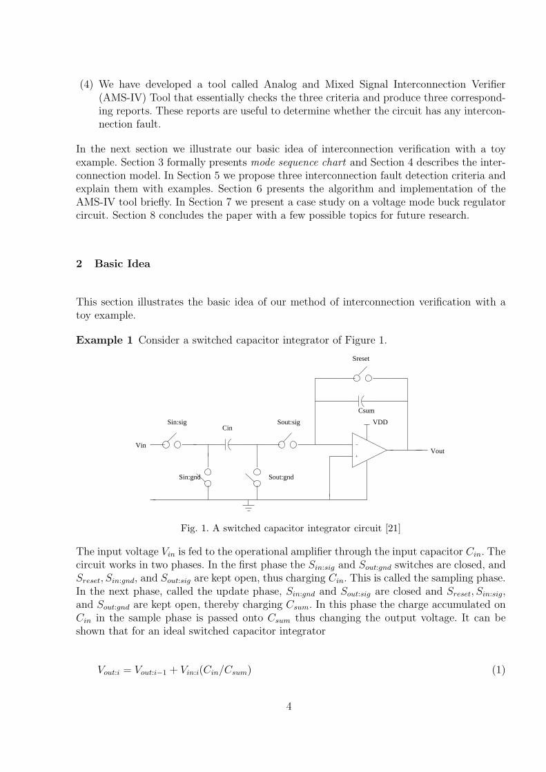
Example 1 Consider a switched capacitor integrator of Figure 1.
Sin:sig
Sin:gnd Sout:gnd
Sout:sig
Csum
Cin
Sreset
VinVout
VDD
+
−
Fig. 1. A switched capacitor integrator circuit [21]
The input voltage Vin is fed to the operational amplifier through the input capacitor Cin. Thecircuit works in two phases. In the first phase the Sin:sig and Sout:gnd switches are closed, andSreset, Sin:gnd, and Sout:sig are kept open, thus charging Cin. This is called the sampling phase.In the next phase, called the update phase, Sin:gnd and Sout:sig are closed and Sreset, Sin:sig,and Sout:gnd are kept open, thereby charging Csum. In this phase the charge accumulated onCin in the sample phase is passed onto Csum thus changing the output voltage. It can beshown that for an ideal switched capacitor integrator
Vout:i = Vout:i−1 + Vin:i(Cin/Csum) (1)
4
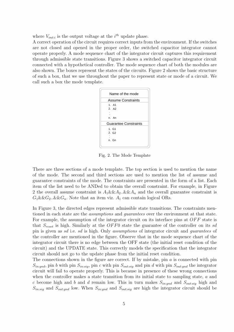
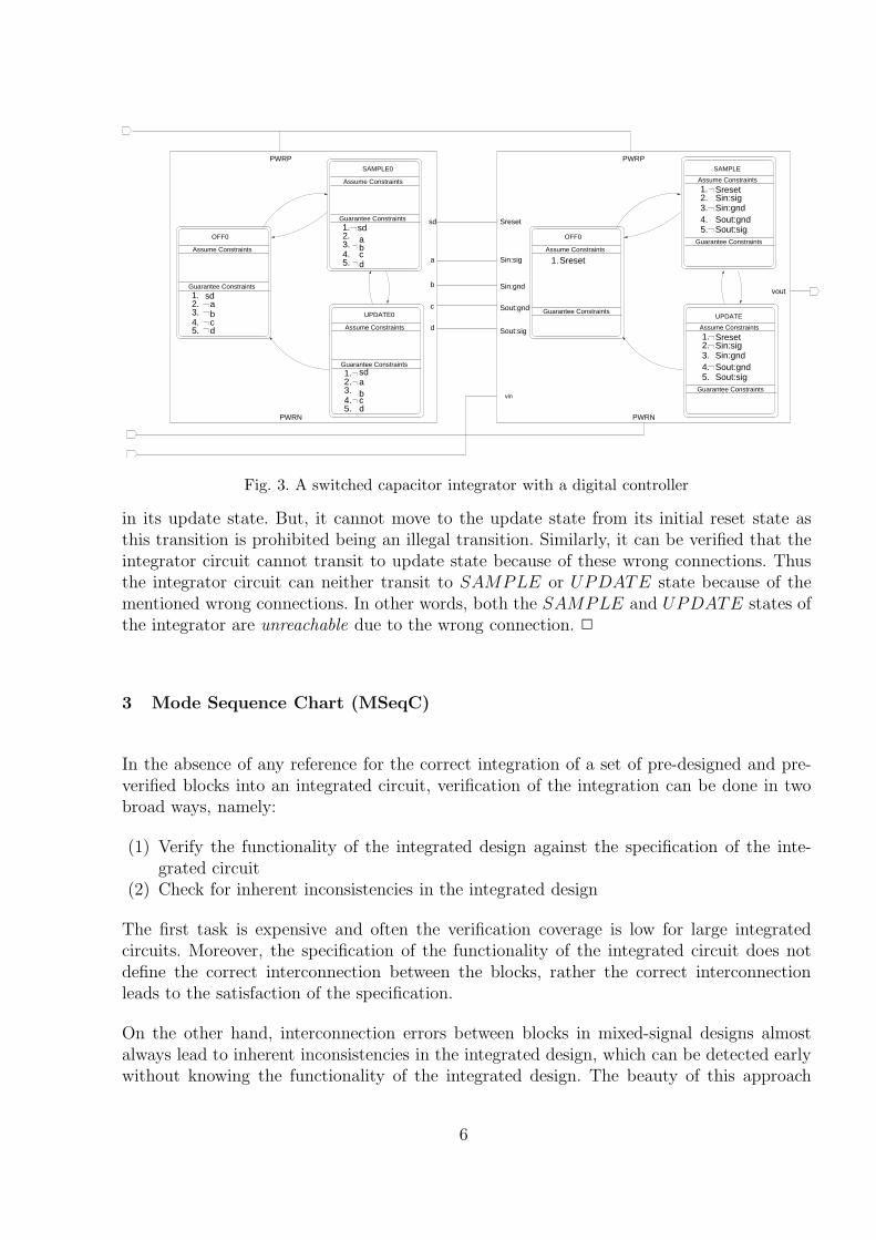
where Vout:i is the output voltage at the ith update phase.A correct operation of the circuit requires correct inputs from the environment. If the switchesare not closed and opened in the proper order, the switched capacitor integrator cannotoperate properly. A mode sequence chart of the integrator circuit captures this requirementthrough admissible state transitions. Figure 3 shows a switched capacitor integrator circuitconnected with a hypothetical controller. The mode sequence chart of both the modules arealso shown. The boxes represent the states of the circuits. Figure 2 shows the basic structureof such a box, that we use throughout the paper to represent state or mode of a circuit. Wecall such a box the mode template.
Assume Constraints
Guarantee Constraints
Name of the mode
1.2.
1.2.
n.
n.
.
.
.
.
A1
An
A2
G1G2
Gn
Fig. 2. The Mode Template
There are three sections of a mode template. The top section is used to mention the nameof the mode. The second and third sections are used to mention the list of assume andguarantee constraints of the mode. The constraints are presented in the form of a list. Eachitem of the list need to be ANDed to obtain the overall constraint. For example, in Figure2 the overall assume constraint is A1&&A2..&&An and the overall guarantee constraint isG1&&G2..&&Gn. Note that an item viz. A1 can contain logical ORs.
In Figure 3, the directed edges represent admissible state transitions. The constraints men-tioned in each state are the assumptions and guarantees over the environment at that state.For example, the assumption of the integrator circuit on its interface pins at OFF state isthat Sreset is high. Similarly at the OFF0 state the guarantee of the controller on its sdpin is given as sd i.e. sd is high. Only assumptions of integrator circuit and guarantees ofthe controller are mentioned in the figure. Observe that in the mode sequence chart of theintegrator circuit there is no edge between the OFF state (the initial reset condition of thecircuit) and the UPDATE state. This correctly models the specification that the integratorcircuit should not go to the update phase from the initial reset condition.The connections shown in the figure are correct. If by mistake, pin a is connected with pinSin:gnd, pin b with pin Sin:sig, pin c with pin Sout:sig and pin d with pin Sout:gnd the integratorcircuit will fail to operate properly. This is because in presence of these wrong connectionswhen the controller makes a state transition from its initial state to sampling state, a andc become high and b and d remain low. This in turn makes Sin:gnd and Sout:sig high andSin:sig and Sout:gnd low. When Sin:gnd and Sout:sig are high the integrator circuit should be
5
Assume Constraints
Guarantee Constraints1.2.3.
5.4.
sd
dc
a
Assume Constraints
UPDATE0
Guarantee Constraints1.2.3.4.5.
sd
ba
dc
OFF0
Assume Constraints
Guarantee Constraints
1.Sreset
vin
Sreset
Sin:sig
Sin:gnd
Sout:gnd
Sout:sig
UPDATE
Assume Constraints
Guarantee Constraints
1.2.3.4.5.
a
b
c
d
PWRN
Assume Constraints
Guarantee Constraints
2.
4.5.
3.
OFF0
1.
SAMPLE0
c
sdab
d
b
PWRN
sd
vout
SresetSin:sigSin:gndSout:gndSout:sig
PWRP PWRPSAMPLE
Assume Constraints
Guarantee Constraints
1.2.3.4.5.
SresetSin:sig
Sout:gndSout:sig
Sin:gnd
Fig. 3. A switched capacitor integrator with a digital controller
in its update state. But, it cannot move to the update state from its initial reset state asthis transition is prohibited being an illegal transition. Similarly, it can be verified that theintegrator circuit cannot transit to update state because of these wrong connections. Thusthe integrator circuit can neither transit to SAMPLE or UPDATE state because of thementioned wrong connections. In other words, both the SAMPLE and UPDATE states ofthe integrator are unreachable due to the wrong connection. 2
3 Mode Sequence Chart (MSeqC)
In the absence of any reference for the correct integration of a set of pre-designed and pre-verified blocks into an integrated circuit, verification of the integration can be done in twobroad ways, namely:
(1) Verify the functionality of the integrated design against the specification of the inte-grated circuit
(2) Check for inherent inconsistencies in the integrated design
The first task is expensive and often the verification coverage is low for large integratedcircuits. Moreover, the specification of the functionality of the integrated circuit does notdefine the correct interconnection between the blocks, rather the correct interconnectionleads to the satisfaction of the specification.
On the other hand, interconnection errors between blocks in mixed-signal designs almostalways lead to inherent inconsistencies in the integrated design, which can be detected earlywithout knowing the functionality of the integrated design. The beauty of this approach
6

lies in choosing a level of abstraction for specifying the functionality of the blocks. We shallshow that many, if not most, of the interconnection errors manifest themselves as inherentinconsistencies if we use simple models of the blocks which capture the macro modes in whichthese blocks function.
Analog and mixed-signal circuits typically function in a set of operating modes. For examplea voltage amplifier typically works in two distinct operating modes: OFF and LINEAR,where OFF represents the cutoff state of the amplifier and LINEAR represents its normalamplifying mode of operation. In each of these operating modes there are various assumptionsand guarantees on the voltage and current values of its interface pins.
It is quite easy for a designer to specify the operating modes of a design block and toenumerate the assumptions and guarantees in each operating mode. For example, designspecifications of a voltage amplifier routinely contain information like input common modevoltage range VICMR, input voltage range VI etc., which specify assumptions about thesignals at the non-inverting and inverting pins. These assumptions are constraints in termsof the voltage at the inverting and non-inverting pins, which are to be guaranteed by thecircuits interfacing with the amplifier to drive the amplifier into its linear mode of operation.Similarly, there are assumptions on input bias current, output load current of the amplifieretc.
Mode Sequence Charts (MSeqC) are simple finite state models of design blocks, where thestates capture the macro modes of operation of a block and a state is annotated with the setof assumptions and guarantees that are expected when that block operates in that mode. Wewill show that many interconnection errors manifest themselves in the form of the followingtypes of inconsistencies in the integrated design, when the blocks are modeled as MSeqCs.The integrated design model is obtained by a parallel composition of the MSeqCs of theblocks.
(1) A reachable state of one MSeqC becomes unreachable in the integrated design model.(2) In a reachable state of the integrated design model, the assumptions required by one
MSeqC is not guaranteed by the others.(3) The set of reachable states of the integrated design model does not cover all the specified
reachable states (given separately). Also, we consider the case where the set of reachablestates of the integrated design model contains one or more undesirable states (also givenseparately).
Our experience shows that the three criteria stated above cover most of the typical intercon-nection errors at the architectural level of large mixed signal integrated circuits. The formaldefinitions follow.
The specification S of a block M is represented by a mode sequence chart, which is a tupleJ =< S, s, τ,Z,A,L,PA,PG > where
• S: set of discrete modes/states of the circuit block.• s: initial state.
7
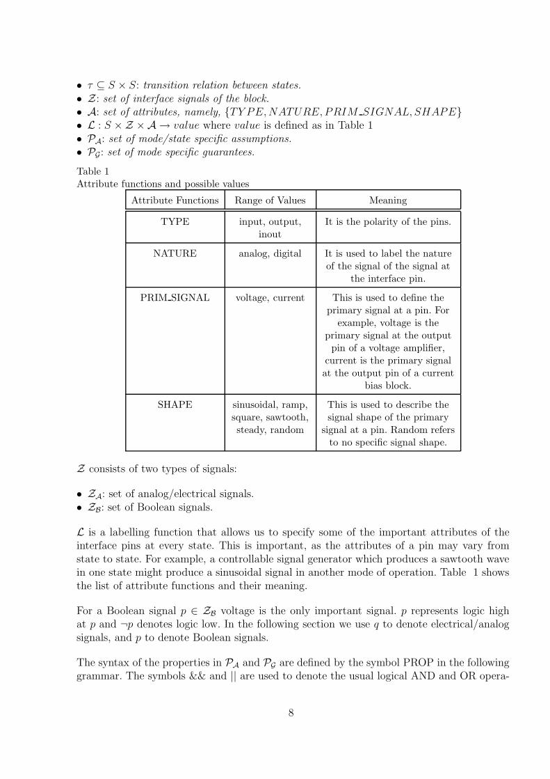
• τ ⊆ S × S: transition relation between states.• Z: set of interface signals of the block.• A: set of attributes, namely, {TY PE,NATURE, PRIM SIGNAL, SHAPE}• L : S ×Z ×A → value where value is defined as in Table 1• PA: set of mode/state specific assumptions.• PG: set of mode specific guarantees.
Table 1Attribute functions and possible values
Attribute Functions Range of Values Meaning
TYPE input, output,inout
It is the polarity of the pins.
NATURE analog, digital It is used to label the natureof the signal of the signal at
the interface pin.
PRIM SIGNAL voltage, current This is used to define theprimary signal at a pin. For
example, voltage is theprimary signal at the outputpin of a voltage amplifier,
current is the primary signalat the output pin of a current
bias block.
SHAPE sinusoidal, ramp,square, sawtooth,steady, random
This is used to describe thesignal shape of the primary
signal at a pin. Random refersto no specific signal shape.
Z consists of two types of signals:
• ZA: set of analog/electrical signals.• ZB: set of Boolean signals.
L is a labelling function that allows us to specify some of the important attributes of theinterface pins at every state. This is important, as the attributes of a pin may vary fromstate to state. For example, a controllable signal generator which produces a sawtooth wavein one state might produce a sinusoidal signal in another mode of operation. Table 1 showsthe list of attribute functions and their meaning.
For a Boolean signal p ∈ ZB voltage is the only important signal. p represents logic highat p and ¬p denotes logic low. In the following section we use q to denote electrical/analogsignals, and p to denote Boolean signals.
The syntax of the properties in PA and PG are defined by the symbol PROP in the followinggrammar. The symbols && and || are used to denote the usual logical AND and OR opera-
8

tors repsectively.
• PROP −→ PROP | B | PROP && PROP | PROP || PROP• CONS −→ TERM REL TERM | CONS || CONS• B −→ B || B | ¬B | p where p∈ ZB
• TERM −→ TERM OP TERM | v(q) | i(q) | f(q) | CONSTANT where CONSTANT ∈ R
• REL −→ > | ≥ | < | ≤ | =• OP −→ + | - | * | /
The meaning of the analog terms are as follows.
• v(q) : The voltage at q with respect to some reference node/ground• i(q) : The current through q out of the module.• f(q) : Frequency of the primary signal at pin q. This can be used to specify a range of
values e.g. 10K < f(q) < 1M or a constant value f(q) = 10K (for example a sinusoidalsignal has constant frequency).
3.1 Example of Modeling Specification with Mode Sequence Chart
An essential module of any portable power management unit (PMU) is a battery charger.Fig 4 shows the block diagram of a battery charger, connected to a battery. A battery chargeris a mixed signal circuit consisting of a digital controller and an analog driver circuit. Thedigital controller, which determines the mode of operation of the analog circuit, is a statemachine whose state transitions are triggered by events from the analog part, that are definedover the voltage (Vbattery) and current (Icharger). Depending on the state, termed fsm state,of the digital controller the charging voltage Vbattery and the charging current Icharger are setby the battery charger.
chargerI
AnalogCircuits
DigitalController
B
batteryV
BatteryCharger
C
Fig. 4. Block Diagram of a Battery Charger
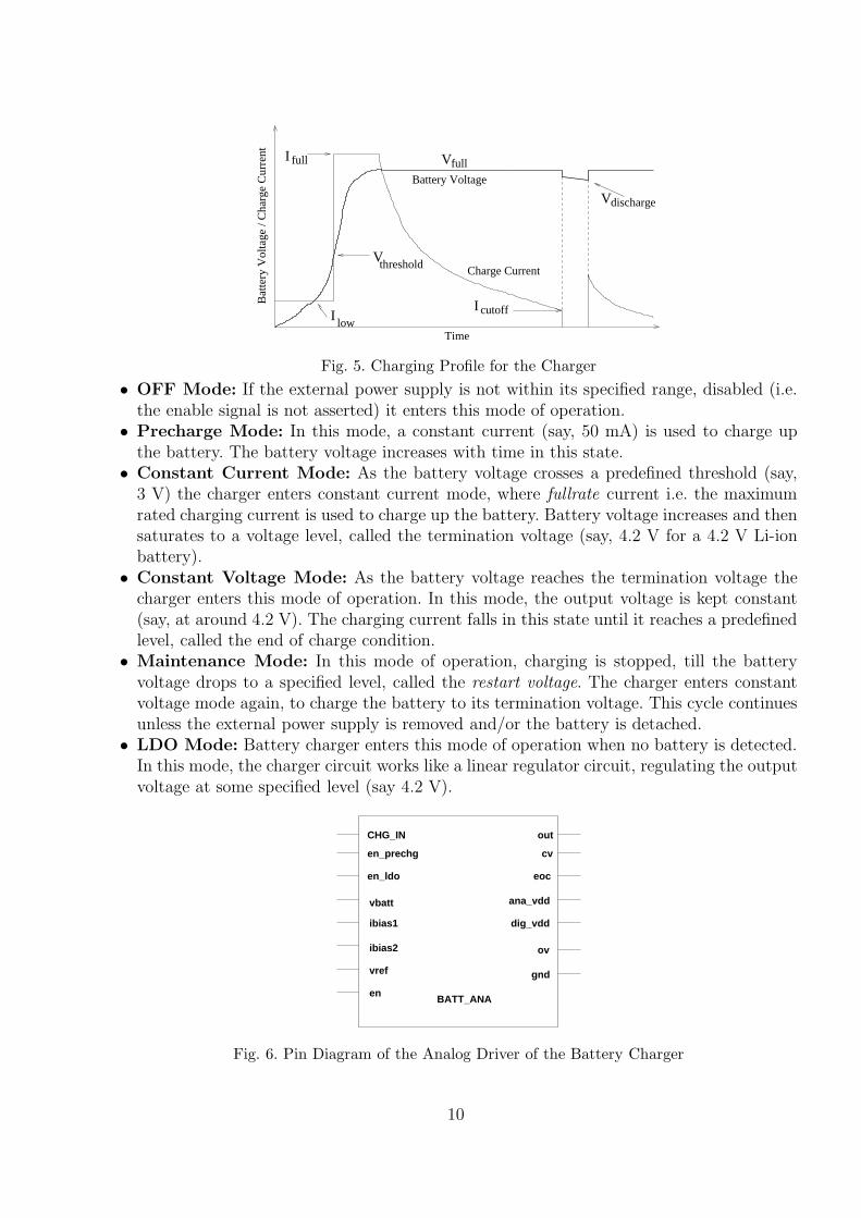
Fig 5 shows a typical charging profile of a battery charger. The charging profile consists ofseveral distinct regions each of which corresponds to a distinct state of the battery charger.These are OFF, precharge, constant current, constant voltage, maintenance and ldo mode.
A brief desription of these modes are given below.
9
Bat
tery
Vol
tage
/ C
harg
e C
urre
nt
Time
Battery Voltage
Vfull
Charge CurrentV
II cutoff
V
I full
threshold
discharge
low
Fig. 5. Charging Profile for the Charger
• OFF Mode: If the external power supply is not within its specified range, disabled (i.e.the enable signal is not asserted) it enters this mode of operation.
• Precharge Mode: In this mode, a constant current (say, 50 mA) is used to charge upthe battery. The battery voltage increases with time in this state.
• Constant Current Mode: As the battery voltage crosses a predefined threshold (say,3 V) the charger enters constant current mode, where fullrate current i.e. the maximumrated charging current is used to charge up the battery. Battery voltage increases and thensaturates to a voltage level, called the termination voltage (say, 4.2 V for a 4.2 V Li-ionbattery).
• Constant Voltage Mode: As the battery voltage reaches the termination voltage thecharger enters this mode of operation. In this mode, the output voltage is kept constant(say, at around 4.2 V). The charging current falls in this state until it reaches a predefinedlevel, called the end of charge condition.
• Maintenance Mode: In this mode of operation, charging is stopped, till the batteryvoltage drops to a specified level, called the restart voltage. The charger enters constantvoltage mode again, to charge the battery to its termination voltage. This cycle continuesunless the external power supply is removed and/or the battery is detached.
• LDO Mode: Battery charger enters this mode of operation when no battery is detected.In this mode, the charger circuit works like a linear regulator circuit, regulating the outputvoltage at some specified level (say 4.2 V).
en_ldo
vbatt
ibias1
vref
out
cv
dig_vdd
ana_vdd
eoc
ibias2
en_prechg
CHG_IN
en
ov
gnd
BATT_ANA
Fig. 6. Pin Diagram of the Analog Driver of the Battery Charger
10
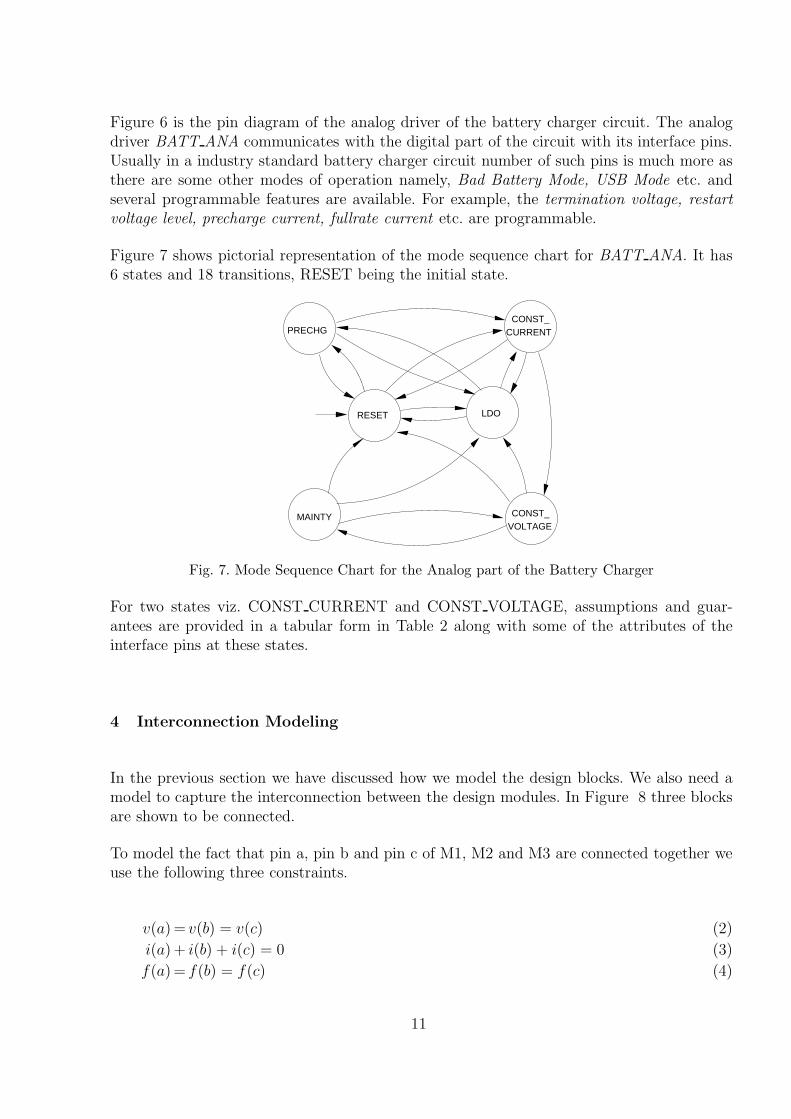
Figure 6 is the pin diagram of the analog driver of the battery charger circuit. The analogdriver BATT ANA communicates with the digital part of the circuit with its interface pins.Usually in a industry standard battery charger circuit number of such pins is much more asthere are some other modes of operation namely, Bad Battery Mode, USB Mode etc. andseveral programmable features are available. For example, the termination voltage, restartvoltage level, precharge current, fullrate current etc. are programmable.
Figure 7 shows pictorial representation of the mode sequence chart for BATT ANA. It has6 states and 18 transitions, RESET being the initial state.
PRECHGCONST_
CURRENT
MAINTYVOLTAGECONST_
RESET LDO
Fig. 7. Mode Sequence Chart for the Analog part of the Battery Charger
For two states viz. CONST CURRENT and CONST VOLTAGE, assumptions and guar-antees are provided in a tabular form in Table 2 along with some of the attributes of theinterface pins at these states.
4 Interconnection Modeling
In the previous section we have discussed how we model the design blocks. We also need amodel to capture the interconnection between the design modules. In Figure 8 three blocksare shown to be connected.
To model the fact that pin a, pin b and pin c of M1, M2 and M3 are connected together weuse the following three constraints.
v(a) = v(b) = v(c) (2)
i(a) + i(b) + i(c) = 0 (3)
f(a) = f(b) = f(c) (4)
11
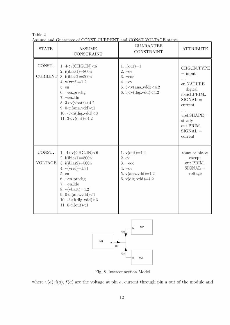
Table 2Assume and Guarantee of CONST CURRENT and CONST VOLTAGE states
STATE ASSUMECONSTRAINT
GUARANTEE
CONSTRAINTATTRIBUTE
CONST
CURRENT
1. 4<v(CHG IN)<62. i(ibias1)=800n3. i(ibias2)=500n4. v(vref)=1.25. en6. ¬en prechg7. ¬en ldo8. 3<v(vbatt)<4.29. 0<i(ana vdd)<110. -3<i(dig vdd)<311. 3<v(out)<4.2
1. i(out)=12. ¬cv3. ¬eoc4. ¬ov5. 3<v(ana vdd)<4.26. 3<v(dig vdd)<4.2
CHG IN.TYPE= input....en.NATURE= digitalibais1.PRIMSIGNAL =current....vref.SHAPE =steadyout.PRIMSIGNAL =current
CONST
VOLTAGE
1.. 4<v(CHG IN)<62. i(ibias1)=800n3. i(ibias2)=500n4. v(vref)=1.3)5. en6. ¬en prechg7. ¬en ldo8. v(vbatt)=4.29. 0<i(ana vdd)<110. -3<i(dig vdd)<311. 0<i(out)<1
1. v(out)=4.22. cv3. ¬eoc4. ¬ov5. v(ana vdd)=4.26. v(dig vdd)=4.2
same as aboveexcept
out.PRIMSIGNAL =
voltage
a
b
c
M1
M2
M3
i(c)
i(b)
i(a)
Fig. 8. Interconnection Model
where v(a), i(a), f(a) are the voltage at pin a, current through pin a out of the module and
12
frequency at pin a.
The first two equations are direct application of Kirchoff’s voltage law (KVL) and Kirchoff’scurrent law (KCL). The current directions shown in Figure 8 are as per the semantics (seesection 3). Equation 4 models the fact the frequency of the signal of the connected pinsmust be same.
Thus, apart from the assume, guarantee constraints at each of the design blocks, we alsohave constraints due to the interconnections. We designate these constraints due to inter-connection by I.
5 Interconnection Fault Detection Criterion and Problem Formulation
While connecting several modules to build up a larger integrated system a wrong connectioncan cause
• Functional Error: Incorrect functional behavior of the overall integrated system. Thiscan happen due to any of the following reasons.· Local Fault: At least one module of the system is not able to behave properly i.e.
Scenario I: either the module is not able to exhibit one of its desired behaviorand/orScenario II: forced to some unspecified state causing it to behave incorrectly.
· Global Fault: Even if there is no local fault the overall behavior of the system candeviate from the correct system level behavior.
• Performance Error: Degradation of performance of the overall system with respect tothe performance specification of the integrated system e.g. more power consumption, morenoisy behavior etc.
A wrong connection can cause any or a combination of the above scenarios. Detection of anysuch faulty scenario indicates presence of one or more number of wrong interconnections inthe integrated circuit.
In the following section we illustrate how functional errors can be detected in our frameworkwhere every module comes with a mode sequence chart.
5.1 Detection of Scenario I
The states of a mode sequence chart represent the operation modes of a circuit. Therefore,failure to reach any state of a module means that the circuit cannot exhibit the functional-ity associated with that state. In other words, when one of the states of an mode sequencechart of a module becomes unreachable, we can say that due to the presence of some wronginterconnection(s) the module can never enter that operating mode (modeled as a state of
13
its mode sequence chart). Hence, the first interconnection fault detection criterion can bestated as follows:
Interconnection Fault Detection Criterion I: Detection of at least one unreachablestate of mode sequence chart of any module M in an integrated system suggests presence ofat least one interconnection fault.
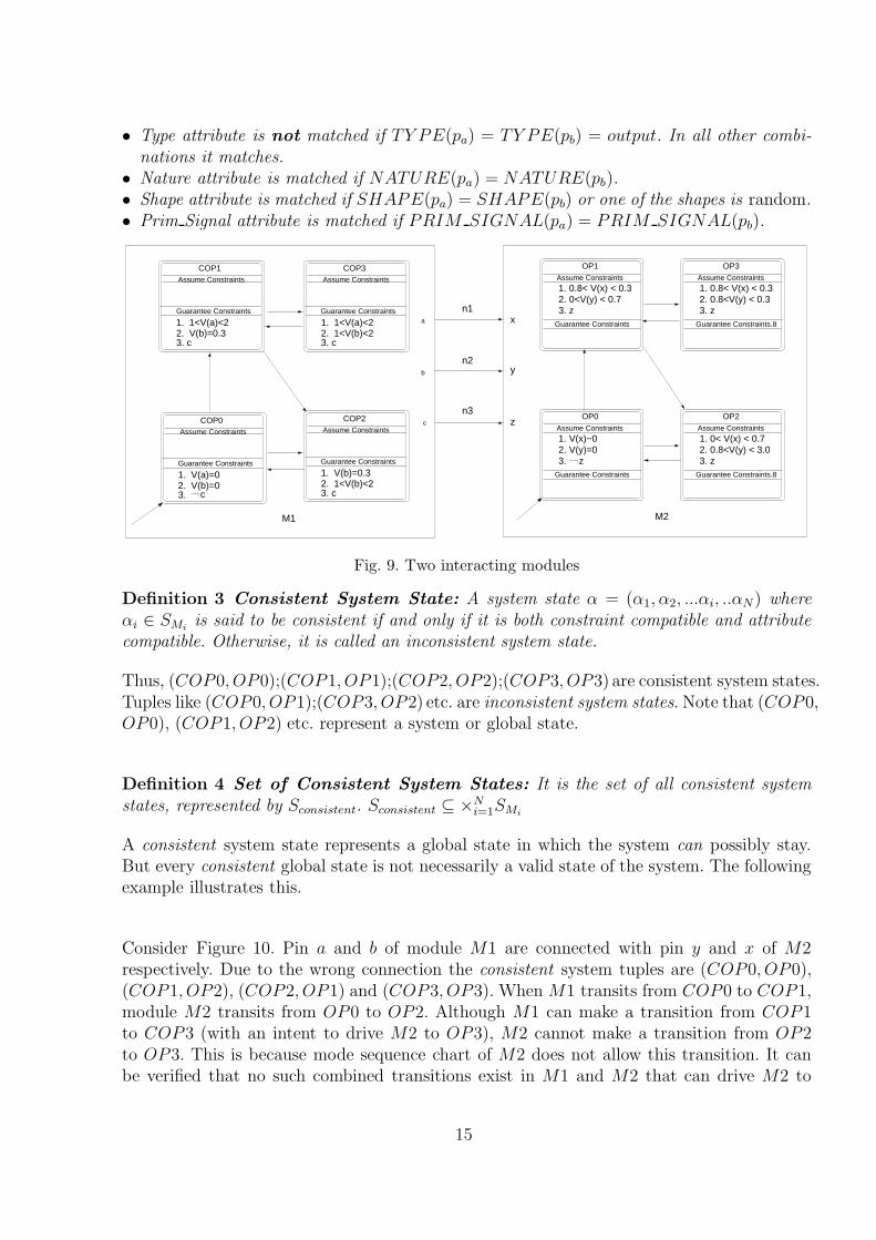
The following example illustrates one scenario where due to interchange of two nets moduleM2 cannot exhibit its desired behavior at state OP3 (see Figure 10) i.e. state OP3 is un-reachable. The connections shown in Figure 9 are correct. Both module M1 and M2 havecertain assumptions and guarantees at its different states. COP0 and OP0 are the initialstates of M1 and M2. Only those guarantees of module M1 and assumptions of M2 whichwould be sufficient to explain are mentioned in Figure 9 and Figure 10.
It may be observed that for the given connections of Figure 9 states COP0 and OP0, COP1and OP1, COP2 and OP2, COP3 and OP3 are compatible with each other. By compatiblewe mean that both constraints and attributes of the two states are compatible as definedbelow.
For a system comprised of N modules M1, M2,...MN a constraint compatible tuple is definedas below. Let SMi
be the set of states of the Mi module.
Definition 1 Constraint Compatible Tuple: A system state α = (α1, α2, ...αi, ..αN ) issaid to be constraint compatible if and only if the following formula is satisfiable.
ψ1 =N∧
i=1
PA(αi)N∧
i=1
PG(αi)∧
I (5)
where αi ∈ SMiand I is the interconnection constraint.
For example, at COP2 the guarantee at output pin a, (V (a) = 0.3) and assumption atOP2 at the connected input pin x, ((V (x) > 0)&&(V (x) < 0.7)) are satisfiable. Similarly,guarantees at pins b and c are satisfiable with the corresponding connected input pins y andz respectively. It can be seen that at COP2 the guarantee at output pin a, (V (a) = 0.3)is not satisfiable with the assumption at OP3 at the connected input pin x, ((V (x) >0.8)&&(V (x) < 3.0)). Hence, COP2 and OP3 are not constraint compatible. Note that forthis example N = 2.
Definition 2 Attribute Compatible: A system state α = (α1, α2, ...αi, ..αN) where αi ∈SMi
is said to be attribute compatible if and only if all the attributes of all the connected pinsof the N modules match according to the following rule. Consider two connected pins pa andpb.
14
• Type attribute is not matched if TY PE(pa) = TY PE(pb) = output. In all other combi-nations it matches.
• Nature attribute is matched if NATURE(pa) = NATURE(pb).• Shape attribute is matched if SHAPE(pa) = SHAPE(pb) or one of the shapes is random.• Prim Signal attribute is matched if PRIM SIGNAL(pa) = PRIM SIGNAL(pb).
OP1
1. 0.8< V(x) < 0.32. 0<V(y) < 0.73. z
Guarantee Constraints
Assume Constraints
1.V(b)=0.3
3. c2.
1<V(a)<2Guarantee Constraints
Assume Constraints
COP1
1.1<V(b)<2
3. c2.
1<V(a)<2Guarantee Constraints
Assume Constraints
COP3
1.V(b)=0
3.2.
V(a)=0Guarantee Constraints
Assume Constraints
COP0
c
1.1<V(b)<2
3. c2.
V(b)=0.3Guarantee Constraints
Assume Constraints
COP2
OP3
1. 0.8< V(x) < 0.32. 0.8<V(y) < 0.33. z
Guarantee Constraints.8
Assume Constraints
OP0
1. V(x)−02. V(y)=03.
Guarantee Constraints
Assume Constraints
z
OP2
1. 0< V(x) < 0.72. 0.8<V(y) < 3.03. z
Guarantee Constraints.8
Assume Constraints
M1
n3
x
M2
n1
n2b
c
a
z
y
Fig. 9. Two interacting modules
Definition 3 Consistent System State: A system state α = (α1, α2, ...αi, ..αN) whereαi ∈ SMi
is said to be consistent if and only if it is both constraint compatible and attributecompatible. Otherwise, it is called an inconsistent system state.
Thus, (COP0, OP0);(COP1, OP1);(COP2, OP2);(COP3, OP3) are consistent system states.Tuples like (COP0, OP1);(COP3, OP2) etc. are inconsistent system states. Note that (COP0,OP0), (COP1, OP2) etc. represent a system or global state.
Definition 4 Set of Consistent System States: It is the set of all consistent systemstates, represented by Sconsistent. Sconsistent ⊆ ×N
i=1SMi
A consistent system state represents a global state in which the system can possibly stay.But every consistent global state is not necessarily a valid state of the system. The followingexample illustrates this.
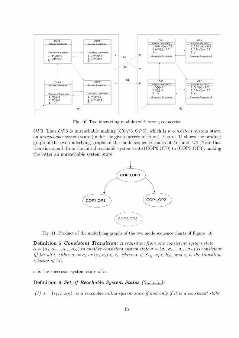
Consider Figure 10. Pin a and b of module M1 are connected with pin y and x of M2respectively. Due to the wrong connection the consistent system tuples are (COP0, OP0),(COP1, OP2), (COP2, OP1) and (COP3, OP3). When M1 transits from COP0 to COP1,module M2 transits from OP0 to OP2. Although M1 can make a transition from COP1to COP3 (with an intent to drive M2 to OP3), M2 cannot make a transition from OP2to OP3. This is because mode sequence chart of M2 does not allow this transition. It canbe verified that no such combined transitions exist in M1 and M2 that can drive M2 to
15
OP1
1. 0.8< V(x) < 0.32. 0<V(y) < 0.73. z
Guarantee Constraints
Assume Constraints
1.V(b)=0.3
3. c2.
1<V(a)<2Guarantee Constraints
Assume Constraints
COP1
1.1<V(b)<2
3. c2.
1<V(a)<2Guarantee Constraints
Assume Constraints
COP3
1.V(b)=0
3.2.
V(a)=0Guarantee Constraints
Assume Constraints
COP0
c
1.1<V(b)<2
3. c2.
V(b)=0.3Guarantee Constraints
Assume Constraints
COP2
OP3
1. 0.8< V(x) < 0.32. 0.8<V(y) < 0.33. z
Guarantee Constraints.8
Assume Constraints
OP0
1. V(x)−02. V(y)=03.
Guarantee Constraints
Assume Constraints
z
OP2
1. 0< V(x) < 0.72. 0.8<V(y) < 3.03. z
Guarantee Constraints.8
Assume Constraints
M1
n3
x
M2
b
c
a
z
y
n1
n2
Fig. 10. Two interacting modules with wrong connection
OP3. Thus OP3 is unreachable making (COP3, OP3), which is a consistent system state,an unreachable system state (under the given interconnection). Figure 11 shows the productgraph of the two underlying graphs of the mode sequence charts of M1 and M2. Note thatthere is no path from the initial reachable system state (COP0,OP0) to (COP3,OP3), makingthe latter an unreachable system state.
COP0,OP0
COP2,OP1 COP1,OP2
COP3,OP3
Fig. 11. Product of the underlying graphs of the two mode sequence charts of Figure 10
Definition 5 Consistent Transition: A transition from one consistent system stateα = (α1, α2, ...αi, ..αN) to another consistent system state σ = (σ1, σ2, ...σi, ..σN) is consistentiff for all i, either αi = σi or (αi, σi) ∈ τi, where αi ∈ SMi
, σi ∈ SMiand τi is the transition
relation of Mi.
σ is the successor system state of α.
Definition 6 Set of Reachable System States (Sreachable):
(1) s = (s1, ....sN ), is a reachable initial system state if and only if it is a consistent state
16
(2) All reachable states from the initial reachable system state s along consistent transitionsare reachable system states.
Definition 7 Reachable Local State: A state σi of module Mi is said to be reachable ifand only if there exists at least one reachable system state σ = (σ1, ...σi, ..σN ).
In the example of Figure 10, Sreachable = {(COP0, OP0), (COP2, OP1), (COP1, OP2)}with (COP0,OP0) the initial reachable system state. Both COP3 and OP3 are unreachablelocal states of modules M1 and M2 respectively.
5.2 Detection of Scenario II
Every circuit is designed with some assumptions on the environment. A voltage regulatorcircuit’s regulation degrades as the load current exceeds its specified (i.e. assumed) value, aswitched capacitor integrator circuit expects that its switches be closed in a proper sequence,a differential amplifier cannot operate as per its specification if the tail bias current is differentfrom its assumed value. A circuit fails to function in an expected fashion if its assumptionsover the environment is violated. This gives us the second interconnection fault detectioncriterion.
Interconnection Fault Detection Criterion II: The assume constraints on the inter-face pins of every module in an integrated system must always be implied by the guaranteeconstraints of the other connected modules (i.e. the environment) at its interface pins. Math-ematically, the following formula has to be valid.
ψ2 = (Genv =⇒ AMi)∧
I (6)
where Genv represents the guarantee of the environment that interacts with module Mi andAMi
is the union of assumptions on its interface pins at each state. I is the interconnectionmodel.
Following example illustrates this fact.
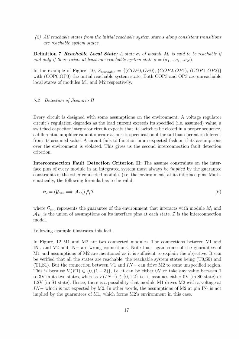
In Figure, 12 M1 and M2 are two connected modules. The connections between V1 andIN-, and V2 and IN+ are wrong connections. Note that, again some of the guarantees ofM1 and assumptions of M2 are mentioned as it is sufficient to explain the objective. It canbe verified that all the states are reachable, the reachable system states being (T0,S0) and(T1,S1). But the connection between V 1 and IN− can drive M2 to some unspecified region.This is because V (V 1) ∈ {0, (1 − 3)}, i.e. it can be either 0V or take any value between 1to 3V in its two states, whereas V (IN−) ∈ {0, 1.2} i.e. it assumes either 0V (in S0 state) or1.2V (in S1 state). Hence, there is a possibility that module M1 drives M2 with a voltage atIN− which is not expected by M2. In other words, the assumptions of M2 at pin IN- is notimplied by the guarantees of M1, which forms M2’s environment in this case.
17
en||V(pwrp)=0||I(iref)=01.2. V(IN+) = 03. V(IN−) = 0
Assume Constraints
S0
Guarantee Constraints
1. enAssume Constraints
S1
3. V(IN−) = 1.2
2. V(pwrp) = 5
4. 0.7<V(IN+)<45. I(iref) = 60u
Guarantee Constraints
sd en
GND pwrn
irefibias
V2
IN+
IN−
V1
pwrpVDD
M1
Assume Constraints
Guarantee Constraints
1. V(VDD) = 0
3. V(V2) = 04.5. I(ibias) = 0
sd
T0
Assume Constraints
Guarantee Constraints
1. V(VDD) = 52. 1<V(V1)<33. V(V2) = 1.24.5. I(ibias) = 60u
T1
vout
2. V(V1) = 0
sd
M2
Fig. 12. Detection of Scenario II
5.3 Detection of Global Fault
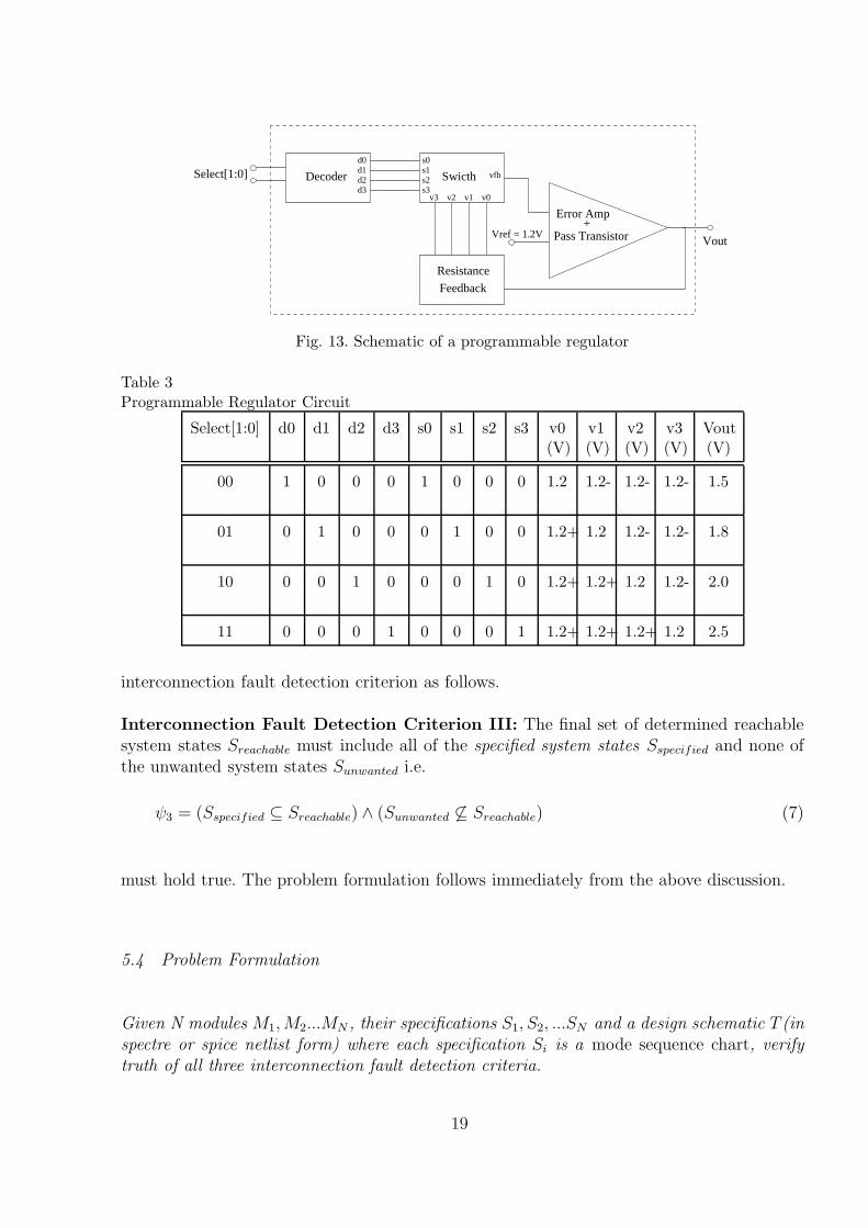
It may happen that none of the above two scenarios of local fault takes place but still oneor more of the system behaviors deviate from its expected behavior. Consider the followingexample of a programmable regulator.
Example 2 Depending on the value of Select[1:0] the regulator circuit operates at fourdifferent voltages. The operation states of the circuit can be described with Table 3. WhenSelect[1:0] = 00 and d0 = 1 the Switch block connects the v0 pin with the vfb pin. Thecircuit output settles at 1.5V, such that v0 is at 1.2V making the error at the input of theerror amplifier 0. Voltage at the other outputs of the Resistance Feedback network is lessthan 1.2V. Similarly, when Select[1:0] = 01. d1 = 1. This makes s1 = 1 (for the correctconnections shown in Figure 13), and the Switch block connects the v1 pin with the vfb pin.The output voltage this time settles at 1.8V, such that v1 is at 1.2V making the error at theinput of the error amplifier 0. v0,v2 and v3 are at different voltage levels other than 1.2V.
Now, if by mistake d0 is connected with s1 and d1 is connected with s0, the circuit behaviorwill change. At Select[1:0] = 00, the output voltage settles to 1.8V instead of 1.5V, and atSelect[1:0]=01, the output voltage settles to 1.5V, instead of 1.8V. So, we can say that dueto the wrong connection, the overall system behavior has changed. 2
But note that this wrong connection cannot be detected with any of the above two criteria.The four rows of table 3 describe the four possible reachable system states. These are thespecified system states of the system. In general, due to interconnection faults many unwantedsystem states can become reachable and desired system states become unreachable. Thus, aspart of global property if Sspecified and Sunwanted represent the set of specified (desired set ofreachable states) and the set of unwanted system states respectively we can state the third
18
Decoder
Feedback
Resistance
Select[1:0]d0d1d2d3
s0s1s2s3
vfb
v3 v1v2 v0
Swicth
Pass Transistor
Error Amp+
VoutVref = 1.2V
Fig. 13. Schematic of a programmable regulator
Table 3Programmable Regulator Circuit
Select[1:0] d0 d1 d2 d3 s0 s1 s2 s3 v0(V)
v1(V)
v2(V)
v3(V)
Vout(V)
00 1 0 0 0 1 0 0 0 1.2 1.2- 1.2- 1.2- 1.5
01 0 1 0 0 0 1 0 0 1.2+ 1.2 1.2- 1.2- 1.8
10 0 0 1 0 0 0 1 0 1.2+ 1.2+ 1.2 1.2- 2.0
11 0 0 0 1 0 0 0 1 1.2+ 1.2+ 1.2+ 1.2 2.5
interconnection fault detection criterion as follows.
Interconnection Fault Detection Criterion III: The final set of determined reachablesystem states Sreachable must include all of the specified system states Sspecified and none ofthe unwanted system states Sunwanted i.e.
ψ3 = (Sspecified ⊆ Sreachable) ∧ (Sunwanted 6⊆ Sreachable) (7)
must hold true. The problem formulation follows immediately from the above discussion.
5.4 Problem Formulation
Given N modules M1,M2...MN , their specifications S1, S2, ...SN and a design schematic T (inspectre or spice netlist form) where each specification Si is a mode sequence chart, verifytruth of all three interconnection fault detection criteria.
19
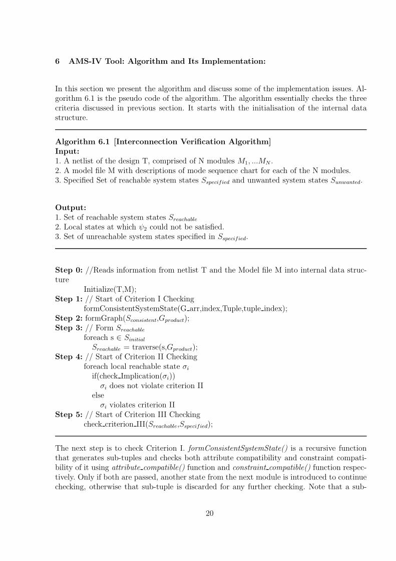
6 AMS-IV Tool: Algorithm and Its Implementation:
In this section we present the algorithm and discuss some of the implementation issues. Al-gorithm 6.1 is the pseudo code of the algorithm. The algorithm essentially checks the threecriteria discussed in previous section. It starts with the initialisation of the internal datastructure.
Algorithm 6.1 [Interconnection Verification Algorithm]Input:1. A netlist of the design T, comprised of N modules M1, ...MN .2. A model file M with descriptions of mode sequence chart for each of the N modules.3. Specified Set of reachable system states Sspecified and unwanted system states Sunwanted.
Output:1. Set of reachable system states Sreachable
2. Local states at which ψ2 could not be satisfied.3. Set of unreachable system states specified in Sspecified.
Step 0: //Reads information from netlist T and the Model file M into internal data struc-ture
Initialize(T,M);Step 1: // Start of Criterion I Checking
formConsistentSystemState(G arr,index,Tuple,tuple index);Step 2: formGraph(Sconsistent,Gproduct);Step 3: // Form Sreachable
foreach s ∈ Sinitial
Sreachable = traverse(s,Gproduct);Step 4: // Start of Criterion II Checking
foreach local reachable state σi
if(check Implication(σi))σi does not violate criterion II
elseσi violates criterion II
Step 5: // Start of Criterion III Checkingcheck criterion III(Sreachable,Sspecified);
The next step is to check Criterion I. formConsistentSystemState() is a recursive functionthat generates sub-tuples and checks both attribute compatibility and constraint compati-bility of it using attribute compatible() function and constraint compatible() function respec-tively. Only if both are passed, another state from the next module is introduced to continuechecking, otherwise that sub-tuple is discarded for any further checking. Note that a sub-
20

tuple of length equal to the number of modules in the integrated system is a possible systemstate. If such a sub-tuple passes both the compatibility checks it is pushed into Sconsistent,the set of consistent system states. Algorithm 6.2 is the description of the function form-ConsistentSystemState().
Algorithm 6.2 [formConsistentSystemState(G arr,index,Tuple,tuple index)]
if(index == number of modules)begin
if(!attribute compatible(Tuple))print ”ATTRIBUTE CHECK FAILED”;
elsebeginif(constraint compatible(Tuple))
push Tuple to Sconsistent
elseprint ”CONSTRAINT CHECK FAILED”;
endendelsebegin
for(each state Si of G arr[index])begin
Tuple[index] = Si;if(!attribute compatible(Tuple))
print ”ATTRIBUTE CHECK FAILED FOR THE SUB TUPLE”;elsebegin
if(constraint compatible(Tuple))formConsistentSystemState(G arr,index + 1,Tuple,tuple index + 1)
elseprint ”CONSTRAINT CHECK FAILED FOR THE SUB TUPLE”;
endend
endreturn;
attribute compatible() checks according to the attribute compatible rules as given in Defini-tion 2. Algorithm 6.3 describes the constraint compatible() function.
21
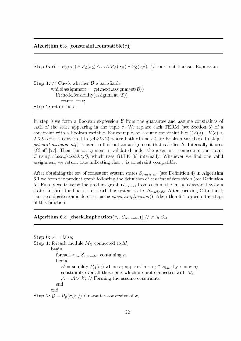
Algorithm 6.3 [constraint compatible(τ)]
Step 0: B = PA(σ1) ∧ PG(σ2) ∧ ... ∧ PA(σN) ∧ PG(σN ); // construct Boolean Expression
Step 1: // Check whether B is satisfiablewhile(assignment = get next assignment(B))
if(check feasibility(assignment, I))return true;
Step 2: return false;
In step 0 we form a Boolean expression B from the guarantee and assume constraints ofeach of the state appearing in the tuple τ . We replace each TERM (see Section 3) of aconstraint with a Boolean variable. For example, an assume constraint like ((V (a) + V (b) <2)&&(en)) is converted to (c1&&c2) where both c1 and c2 are Boolean variables. In step 1get next assignment() is used to find out an assignment that satisfies B. Internally it useszChaff [27]. Then this assignment is validated under the given interconnection constraintI using check feasibility(), which uses GLPK [9] internally. Whenever we find one validassignment we return true indicating that τ is constraint compatible.
After obtaining the set of consistent system states Sconsistent (see Definition 4) in Algorithm6.1 we form the product graph following the definition of consistent transition (see Definition5). Finally we traverse the product graph Gproduct from each of the initial consistent systemstates to form the final set of reachable system states Sreachable. After checking Criterion I,the second criterion is detected using check implication(). Algorithm 6.4 presents the stepsof this function.
Algorithm 6.4 [check implication(σi, Sreachable)] // σi ∈ SMj
Step 0: A = false;Step 1: foreach module MK connected to Mj
beginforeach τ ∈ Sreachable containing σi
beginX = simplify PA(σl) where σl appears in τ σl ∈ SMk
, by removingconstraints over all those pins which are not connected with Mj .A = A∨ X ; // Forming the assume constraints
endend
Step 2: G = PG(σi); // Guarantee constraint of σi
22
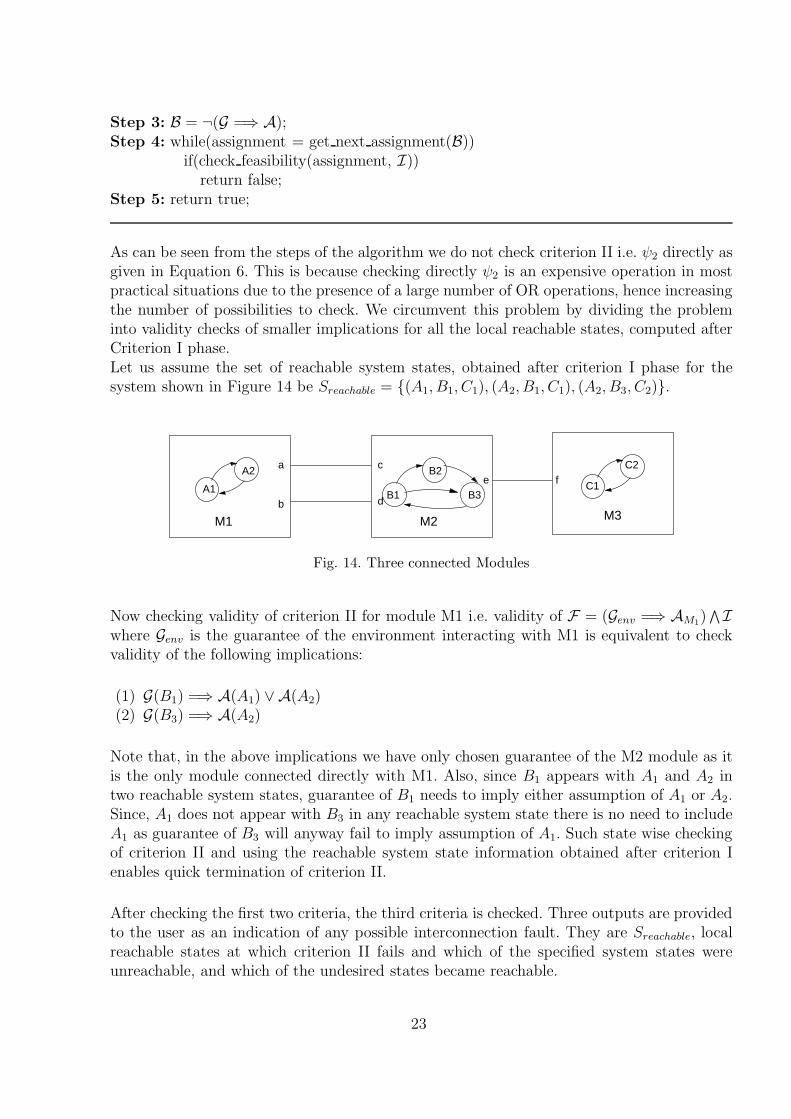
Step 3: B = ¬(G =⇒ A);Step 4: while(assignment = get next assignment(B))
if(check feasibility(assignment, I))return false;
Step 5: return true;
As can be seen from the steps of the algorithm we do not check criterion II i.e. ψ2 directly asgiven in Equation 6. This is because checking directly ψ2 is an expensive operation in mostpractical situations due to the presence of a large number of OR operations, hence increasingthe number of possibilities to check. We circumvent this problem by dividing the probleminto validity checks of smaller implications for all the local reachable states, computed afterCriterion I phase.Let us assume the set of reachable system states, obtained after criterion I phase for thesystem shown in Figure 14 be Sreachable = {(A1, B1, C1), (A2, B1, C1), (A2, B3, C2)}.
a
b
c
d
M1
e fB2
B3C1
C2
B1
A2
A1
M2 M3
Fig. 14. Three connected Modules
Now checking validity of criterion II for module M1 i.e. validity of F = (Genv =⇒ AM1)∧I
where Genv is the guarantee of the environment interacting with M1 is equivalent to checkvalidity of the following implications:
(1) G(B1) =⇒ A(A1) ∨A(A2)(2) G(B3) =⇒ A(A2)
Note that, in the above implications we have only chosen guarantee of the M2 module as itis the only module connected directly with M1. Also, since B1 appears with A1 and A2 intwo reachable system states, guarantee of B1 needs to imply either assumption of A1 or A2.Since, A1 does not appear with B3 in any reachable system state there is no need to includeA1 as guarantee of B3 will anyway fail to imply assumption of A1. Such state wise checkingof criterion II and using the reachable system state information obtained after criterion Ienables quick termination of criterion II.
After checking the first two criteria, the third criteria is checked. Three outputs are providedto the user as an indication of any possible interconnection fault. They are Sreachable, localreachable states at which criterion II fails and which of the specified system states wereunreachable, and which of the undesired states became reachable.
23
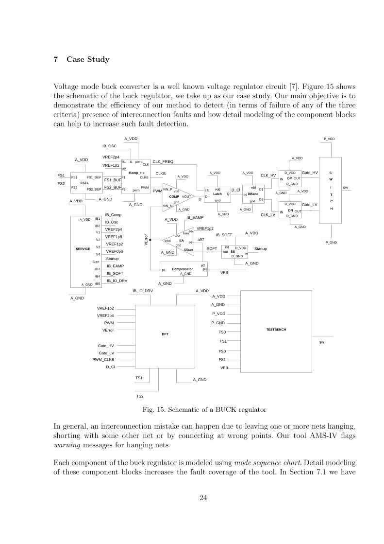
7 Case Study
Voltage mode buck converter is a well known voltage regulator circuit [7]. Figure 15 showsthe schematic of the buck regulator, we take up as our case study. Our main objective is todemonstrate the efficiency of our method to detect (in terms of failure of any of the threecriteria) presence of interconnection faults and how detail modeling of the component blockscan help to increase such fault detection.
VREF2p4
VREF1p8
IB_Osc
IB_Comp
VREF1p2
VREF0p6
Startup
IB_EAMP
IB_SOFT
IB_IO_DRV
A_VDD
A_GND
Startup
IB_SOFT A_VDD
A_GND
VREF1p2
A_VDD
A_GND
IB_IO_DRV
TS1
TS2
TS0
A_VDD
A_GND
P_VDD
P_GND
TS1
FS0
FS1
VFB
Gate_HV
Gate_LV
PWM_CLKB
VError
PWM
VREF2p4
VREF1p2
sw
FS2
FS1
A_VDD
A_GNDA_GND
A_VDD
FS1_BUF
FS2_BUF
VREF1p2
VREF2p4
IB_OSC
CLK_FREQ
CLKB
PWM
A_VDD
A_GND
VFB
sw
Gate_HV
Gate_LV
VE
rror
D
D_Cl
CLK_LV
CLK_HV
A_GND
FS2_BUF
FS1
FS2
FS1_BUF
A_GND
A_VDD IB1
IB2
V1
V2
V3
V4
Start
IB3
IB4
IB5
PWM
CLKB
CLKR1
R2
F2
F1
pwrp
pwrn
I1
VIN_P
VIN_N
VOUTCOMP
gndvout
vddbiasIN+
SStart
IN−
SOFT
FSEL
SERVICE
IN OUT
IN OUT
IN
O1
O2
clkQ DBandLatch
out in
in1 D_VDD
P_VDD
P_GND
A_VDD
A_GND A_VDD
A_GND
SSD_GND
D_VDD
D_GND
D_VDD
D_GND
A_GNDp1
p2p3
A_VDD
A_GNDA_GND
A_VDD
D
Compensator
Ramp_clkA_VDD
A_GND
gnd
vdd
IB_EAMP
DP
DN
I
T
C
H
W
S
EA
TESTBENCHDFT
a97
vdd
gnd
vdd
gnd
D_Cl
Fig. 15. Schematic of a BUCK regulator
In general, an interconnection mistake can happen due to leaving one or more nets hanging,shorting with some other net or by connecting at wrong points. Our tool AMS-IV flagswarning messages for hanging nets.
Each component of the buck regulator is modeled using mode sequence chart. Detail modelingof these component blocks increases the fault coverage of the tool. In Section 7.1 we have
24

discussed with an example how a simpler (less detail) model of a component can affect thefault coverage. The results shown in Table 4 are carried out with a very detail model of eachof the component. The total state space, calculated by taking cartesian product of the setof states of the underlying graphs of each of the block’s mode sequence charts is 28 million.It should be borne in mind that depending on specification number of states in each MSeqCcan change, and that changes the total state space and hence the run time for the tool.
Table 4 is a list of some of the interconnection faults and which of the criteria failed toindicate presence of the faults. User time is reported in the last column of the table. Thefirst row corresponds to the scenario where no fault has been injected.
In another experiment we injected faults of different classes and observed the fault cover-age for each such fault-class. There are typically 5 classes of faults in a circuit like BUCKregulator. They are
(1) Power Class: In this class all the power nets belong e.g. the nets connected with powersupply and ground pins.
(2) Bias Class: Nets connected with the pins, which are used for bias supply (referencevoltage, bias voltage, bias current) belong to this category.
(3) Control Signal Class: These are the digital nets used for controlling purpose. For exam-ple, enable, clock signals belong to this class.
(4) Digital Signal Class: These are the other digital nets. In Figure 15 FS1, FS2 connectedwith the FSEL block are two such nets.
(5) Analog Signal Class: These are the analog nets other than the nets that belong to powerand bias classes. In Figure 15 such pins are PWM of Ramp clk block, VOUT of the EA(error amplifier) block etc.
We injected single faults by interchanging two nets of same class at a time. For example, weconnected the PWM of Ramp clk block to the VIN N of the COMP block and connectedthe VOUT pin of the EA block with the VIN P of the COMP block to inject a fault of theAnalog Signal class. We injected all such possible single faults of each class and observed thefault coverage for each class. Table 5 reports the fault coverage results we obtained. It showsan overall fault coverage of 92%.
7.1 Writing Specifications
The success of the method depends on correct and detail specification of the components.Incomplete specifications like less number of modes of operations and/or relaxed constraintscan make the method miss interconnection faults. For example, the deadband block (DBandof Figure 15) is mainly a delay block that produces two clock signals namely CLK HV andCLK LV with some delay with respect to the input clock singal i.e. D CL. Figure 16 describesthe behavior of the deadband block.
Figure 17 shows one possible MSeqC for it. Since the outputs O1 and O2 can be either in
25
Table 4Fault Detection with AMS-IV Tool
Scenario Manifestation Time
Criterion 1 Criterion2 Criterion 3
NO FAULT Passed with 49reachable system
states.
Passed Passed 840
a97 and VErrorof Compensator
block areswapped
Failed. Onereachable system
state only
Passed Failed 792
VREF1p2 andVREF2p4 ofRamp clk are
swapped
Failed. Onereachable system
state.
Passed Failed 11
Gate HV andGate LV are
swapped
Failed. 33reachable states,
with no statestarting with DB3
Passed Failed 742
SOFT and a97are swapped
Failed. Onereachable state
only.
Passed Failed 780
A VDD of DPblock shorted to
ground
Failed. Onereachable system
state
Passed Failed 508
PWM andVError of COMPare interchanged
Failed. Onereachable system
state.
Passed Failed 7
VError shorted toA GND
Failed. Noreachable system
state
Passed Failed 6
Latch output isdisconnected fromDBand. InsteadCOMP’s outputwas connected to
it.
Passed Failed Failed. 1147
00, 10 and 11 state (see Figure 16), and the input IN can be either 1 or 0 and hence noconstraint on IN has been mentioned.
Since the model does not have any constraint on the input pin IN, such a specification cannot
26
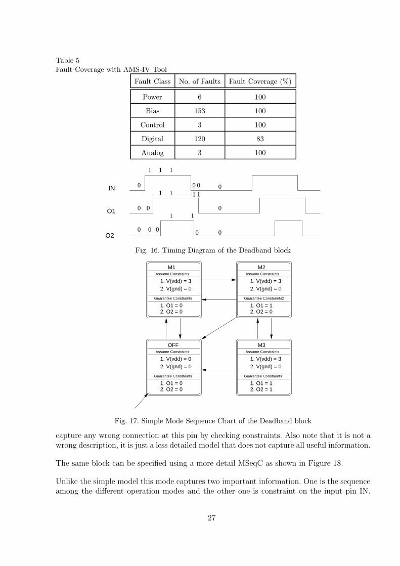
Table 5Fault Coverage with AMS-IV Tool
Fault Class No. of Faults Fault Coverage (%)
Power 6 100
Bias 153 100
Control 3 100
Digital 120 83
Analog 3 100
0
0
0 0
1
0
0
0 0
0
0
1
1
1
0
1
1
1
1
01
O2
O1
IN
Fig. 16. Timing Diagram of the Deadband block
2. O2 = 01. O1 = 0
Guarantee Constraints
OFF
2. V(gnd) = 0
Assume Constraints
1. V(vdd) = 0
2. O2 = 01. O1 = 0
Guarantee Constraints
M1
2. V(gnd) = 0
Assume Constraints
1. V(vdd) = 3
2. O2 = 01. O1 = 1
Guarantee Constraints2
M2
2. V(gnd) = 0
Assume Constraints
1. V(vdd) = 3
2. O2 = 11. O1 = 1
Guarantee Constraints
M3
2. V(gnd) = 0
Assume Constraints
1. V(vdd) = 3
Fig. 17. Simple Mode Sequence Chart of the Deadband block
capture any wrong connection at this pin by checking constraints. Also note that it is not awrong description, it is just a less detailed model that does not capture all useful information.
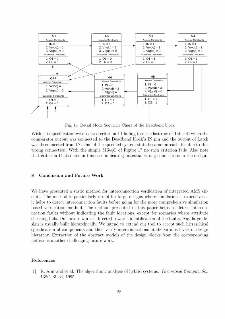
The same block can be specified using a more detail MSeqC as shown in Figure 18.
Unlike the simple model this mode captures two important information. One is the sequenceamong the different operation modes and the other one is constraint on the input pin IN.
27
2. O2 = 01. O1 = 0
Guarantee Constraints
OFF
2. V(gnd) = 0
Assume Constraints
1. V(vdd) = 0
Guarantee Constraints
3. V(gnd) = 02. V(vdd) = 01. IN = 0Assume Constraints
1. O1 = 02. O2 = 0
M1
Guarantee Constraints
3. V(gnd) = 02. V(vdd) = 31. IN = 1Assume Constraints
1. O1 = 02. O2 = 0
M2
Guarantee Constraints
3. V(gnd) = 02. V(vdd) = 31. IN = 1Assume Constraints
1. O1 = 12. O2 = 0
M3
Guarantee Constraints
3. V(gnd) = 02. V(vdd) = 31. IN = 1Assume Constraints
1. O1 = 12. O2 = 1
M4
Guarantee Constraints
3. V(gnd) = 02. V(vdd) = 31. IN = 0Assume Constraints
1. O1 = 12. O2 = 1
M5
Guarantee Constraints
3. V(gnd) = 02. V(vdd) = 31. IN = 0Assume Constraints
1. O1 = 12. O2 = 0
M6
Fig. 18. Detail Mode Sequence Chart of the Deadband block
With this specification we observed criterion III failing (see the last row of Table 4) when thecomparator output was connected to the Deadband block’s IN pin and the output of Latchwas disconnected from IN. One of the specified system state became unreachable due to thiswrong connection. With the simple MSeqC of Figure 17 no such criterion fails. Also notethat criterion II also fails in this case indicating potential wrong connections in the design.
8 Conclusion and Future Work
We have presented a static method for interconnection verification of integrated AMS cir-cuits. The method is particularly useful for large designs where simulation is expensive asit helps to detect interconnection faults before going for the more comprehensive simulationbased verification method. The method presented in this paper helps to detect intercon-nection faults without indicating the fault locations, except for scenarios where attributechecking fails. Our future work is directed towards identification of the faults. Any large de-sign is usually built hierarchically. We intend to extend our tool to accept such hierarchicalspecification of components and then verify interconnections at the various levels of designhierarchy. Extraction of the abstract models of the design blocks from the correspondingnetlists is another challenging future work.
References
[1] R. Alur and et al. The algorithmic analysis of hybrid systems. Theoretical Comput. Sc.,138(1):3–34, 1995.
28
[2] A. Balivada and et al. Verification of transient response of linear analog circuits. InIEEE VLSI Test Symposium, pages 42–47, 1995.
[3] T. Dang, A. Donze, and O. Maler. Verification of Analog and Mixed-Signal CircuitsUsing Hybrid System Techniques. Formal Methods In Computer-aided Design: 5th In-ternational Confrence, FMCAD, 2004.
[4] T. Dastidar and P. Chakrabarti. A verification system for transient response of analogcircuits using model checking. In VLSI: Proc. of the 18th Int. Conf. on VLSI Design,2005.
[5] R. David and H. Alla. On hybrid petri nets. Discrete Event Dynamic Systems, 11(1-2):9–40, 2001.
[6] L. de Alfaro and T. Henzinger. Interface automata. Proceedings of the 8th Europeansoftware engineering conference held jointly with 9th ACM SIGSOFT international sym-posium on Foundations of software engineering, pages 109–120, 2001.
[7] R. Erickson and D. Maksimovic. Fundamentals of Power Electronics. Kluwer AcademicPublishers, 2001.
[8] A. Ghosh and R. Vemuri. Formal verification of synthesized analog designs. Interna-tional Conference on Computer Design, pages 40–45, 1999.
[9] GLPK. GNU Linear Programming Kit http://www.gnu.org/software/glpk/.[10] S. Gupta, B. Krogh, and R. Rutenbar. Towards formal verification of analog designs.
ICCAD, pages 210–217, 2004.[11] K. Hanna. Reasoning about real circuits. In Proc. 7th International Higher Order Logic
Theorem Proving and Its Applications Conference, pages 235–253, 1994.[12] K. Hanna. Reasoning About Analog-Level Implementations of Digital Systems. Formal
Methods in System Design, 16(2):127–158, 2000.[13] D. Harel and et al. Statecharts: A visual formalism for complex systems. Science of
Computer Programming, 8(3):231–274, 1987.[14] W. Hartong, R. Klausen, and L. Hedrich. Formal Verification for Nonlinear Analog Sys-
tems: Approaches to Model and Equivalence Checking. Advanced Formal Verification,pages 205–245, 2004.
[15] L. Hedrich and E. Barke. A formal approach to verification of linear analog circuitswith parameter tolerances. In IEEE/ACM DATE, pages 649–654, 1998.
[16] T. Henzinger, P. Ho, and H. Wong-Toi. HYTECH: a model checker for hybrid systems.International Journal on Software Tools for Technology Transfer (STTT), 1(1):110–122,1997.
[17] A. Jesser, T. Kropf, and et al. Analog Simulation Meets Digital Verification - A FormalAssertion Approach for Mixed-Signal Verification. SASIMI, pages 507–514, 2007.
[18] N. Lynch, R. Segala, F. Vaandrager, and H. Weinberg. Hybrid IO automata. HybridSystems III: Verification and Control, LNCS, 1066:496510, 1996.
[19] O. Maler. Extending PSL for Analog Circuits. Research Report, PROSYD DeliverableD, 1(1), 2005.
[20] MSC. Message Sequence Chart http://www.sdl-forum.org/MSC/index.htm.[21] M. Pastre and M. Kayal. Methodology for the Digital Calibration of Analog Circuits
And Systems: With Case Studies. Springer, 2006.[22] R. O. Peruzzi. Verification of Digitally Calibrated Analog Systems with Verilog-AMS
Behavioral Models. Behavioral Modeling and Simulation Workshop, pages 7–16, 2006.
29

[23] A. Salem. Semi-formal verification of VHDL-AMS descriptions. ISCAS, 5, 2002.[24] Verilog. http://www.verilog.com/IEEEVerilog.html.[25] VerilogA. http://www.eda.org/verilog-ams.[26] Virtuoso Schematic Editor. http://www.cadence.com/products/custom ic/
vschematic/index.aspx.[27] zChaff. An Efficient SAT Solver "http://www.princeton.edu/~chaff/zchaff.html.
30