a study of the silicon bulk-barrier diodes designed in
TRANSCRIPT

157
Research Article
A study of the silicon Bulk-Barrier Diodes designed in planar technology by means of simulation
P. Papadopoulou1,* and L. Georgopoulos2 1Department of Science, Technological Educational Institute of Kavala, St. Loukas 65404 Kavala, Greece.
2Department of Electrical Engineering, Technological Educational Institute of Kavala, St. Loukas 65404 Kavala, Greece.
Received 11 May 2009; Revised 9 November 2009; Accepted 2 December 2009
Abstract
In this paper, it is studied for the first time, the possibility of manufacturing a Bulk Barrier diode in planar technology using simulation. This study is based on simulation results obtained with a 2-D device simulator (S-PISCES). More precisely, the electrical and switching behavior of the proposed devices in planar technology were investigated. The results of this study show that the technological parameters (doping concentrations), as well as the geometrical sizes (middle region width) and the bias conditions (applied voltage), have significant effects on the electrical and switching behavior of the proposed devices. The appropriate choice of these parameters can reduce the switching time in the range of few picoseconds and also dramatically modify the current through the device. The simulation results of devices in planar technology have been compared with those designed in non planar technology. Finally, good agreement among theory and simulations results of the proposed devices observed.
Keywords: Device Simulation, electrical behaviour, Switching behaviour, Bulk-Barrier Diodes, planar technology.
Journal of Engineering Science and Technology Review 2 (1) (2009) 157-164
JOURNAL OFEngineering Science and Technology Review
www.jestr.org
Bulk- Barrier Diodes (BBD’s) [1, 2], or Camel Diodes (CD’s) [3,4], are two - terminal three-layer structures similar to Bipolar Junction Transistor (BJT), where the current is controlled by a potential barrier located inside the semiconductor. However, con-trary to the BJT’s, the middle (base) region in BBD’s is so thin that it is normally fully depleted from free carriers and there exists no neutral region. Similar structures appear in the literature with dif-ferent names: “Bulk Unipolar Diodes” [5-7], “Triangular Barrier Diodes” [8], and “P-plane Diodes” [7]. All the above structures are, like Schottky diodes, in majority carrier devices and therefore can be used for high-speed applications. Contrary to the Schottky diodes, BBD’s offer the possibility to control the barrier height by well controllable technological parameters, such as dopant concen-tration and middle layer width. This advantage over the classical Schottky diode makes them very attractive in many applications. There are several published works referring to the applications of such structures as photodiodes with high internal gain [4, 9], high speed optoelectronic switches [10,-16], temperature sensors [17], Bulk- Barrier Transistors [18], gates in FET’s [19] and high speed devices [20]. All the above published works refer to devices that are designed in non planar technology.
In the present work we study for the first time the possibil-
ity of manufacturing a Bulk Barrier diode in planar technology using simulation. To be more specific, we investigate the electrical and switching behavior of devices in planar technology using ad-vanced simulation packages (S-PISCES). The simulation results of devices in planar technology are given and compared to those in non planar technology. Additionally, the simulation results were used to verify the validity of the analytical model [2, 20] in the case of devices manufactured in planar technology.
2. Theoretical analysis
Fig.(1) shows the structure of the BBD in non planar technology and the distribution of space charge density, ρ(x), electric field, E(x) and electrostatic potential, V(x), under equilibrium (
)
as well as under forward ( ) and reverse bias conditions ( ). Total depletion of the n layer, achieved by proper choice of the thickness and doping concentration of the middle layer, is a prerequisite for BBD operation [2]. It is also assumed that the three layers are uniformly doped with concentrations: NC in the substrate layer (collector), NB in the middle layer (base) and NE in the sur-face layer (emitter). The solution of Poisson’s equation in thermal equilibrium leads to a potential barrier height, ΦBL0, given by:
* E-mail address: [email protected] ISSN: 1791-2377 © 2009 Kavala Institute of Technology. All rights reserved.
1. Introduction

158
P. Papadopoulou and L. Georgopoulos /Journal of Engineering Science and Technology Review 2 (1) (2009) 157-164
(1)
With (2)
where d is the middle layer thickness, q is the electron charge, is the electron mean density distribution in the middle layer, ε = ε0εr is the dielectric constant and VD is the difference between the Fermi-level potentials in the p+ and p layers and it is given by:
(3)
where VT = kT/q. When the middle layer is fully depleted from free carriers Eq.(2) it takes the following form [2]:
(4)
Fig.(1d) shows qualitatively the variation of the potential barrier under bias conditions. For reverse bias (i.e. + on the emitter and – on the collector), the depletion layer width within the substrate expands and the potential barrier height on the right side of the middle layer ΦBR, increases. At the same time the potential barrier on the left side ΦBL, decreases, and so in this case the hole current over this barrier dominates. The opposite is valid for forward bias, where the hole current over the barrier ΦBR dominates. Eq.(1) for ΦBL under bias conditions takes the form:
(5)
where the ± signs are for the forward and the reverse bias condi-tions, respectively
Under forward bias conditions, the barrier height ΦBR may be expressed in terms of the ΦBL and the bias voltage by the equa-tion:
(6)
provided that the applied voltage drops entirely in the collector junction.
Substituting Eq.(6) in Eq.(5) gives:
(7)
Analytic Current – Voltage characteristics
The current in BBD’s depend strongly on the mean free path of charge carriers. If the majority of charge carriers pass the potential barrier Φ without collision, the resulting current can be calcu-lated based on the thermionic emission theory [3]. Otherwise, the drift-diffusion theory will apply [1]. In the intermediate case, the thermionic emission – drift-diffusion theory is valid [3]. All three theories define the current passing over a barrier as follows:
(8)
The current is an exponential function of the barrier height Φ, regardless of the mean free path of charge carriers. The differ-ence between the various theories is expressed by the differences in saturation current IS.
According to Eq.(8), carriers in a BBD that have to over-
Figure 1. (a) Structure of the BBD, (b) space charge density distribution ρ(x), (c) electric field distribution E(x), and (d) electrostatic potential distribu-tion V(x), in thermal equilibrium ( ), with a positive applied voltage ( ), and with a negative applied voltage ( ).
( ) ( )[ ]TS VVkTqII exp1exp −⋅Φ⋅−⋅=

159
come the lowest barrier contribute mostly to the current. In the forward bias the current through the diode is given by:
(9)
for
where ISF is the saturation current in forward bias given by:
(9.1)
where A is the cross-section area, Dp and Dn are the diffusion coefficients for holes and electrons, respectively, LD is the Debye length, and uth is the thermal velocity.
Following the same procedure, as for Eq.(9), the reverse bias current can be expressed by:
(10)
Where ISR is the saturation current in reverse bias given by:
(10.1)
From Eq.(9.1) and (10.1) it is obvious that
Switching behavior analytical model
For switching applications, the transition from a conducting to a non-conducting state (e.g. from forward to zero bias) must be nearly abrupt and the transient time must be short. In the case of a Bulk Barrier Diode (BBD) when the bias voltage is switched from a forward voltage VF to zero voltage, the current through the diode changes abruptly from IF to a reverse current IR which afterwards decays exponentially to IS within a certain time. The switching time is defined as the time in which the device current reaches 10% of its initial value IR. Several mechanisms can extend
this switching time. According to [20] the total switching time for BBD’s is given by:
(11)
Where:
τSTOR is the storage time of minority carriers (electrons) on the edges of the depletion region, τTRAP is the trapping time of free electrons in the potential well, τTRAN is the transit time of free carriers travelling through the depletion region and τRC is the de-pletion layer discharging time. This is the time required to dis-charge the depletion capacitance CD, through a finite resistance R (τ=R*CD).
According to [20] the switching time of BBDs is mainly de-termined by the depletion layer discharging time. This is associ-ated with the finite time that takes to modulate the space charge in the depletion region. This has to be done by injecting an input current that discharges the depletion capacitance CD, through a finite resistance R. Therefore the total switching time for BBDs is given by:
(12)
Eqs. (9) and (10) show that the current through the BBD in-creases exponentially with the applied voltage in both bias condi-tions. This is valid only for the case in which the injected carrier charge in the depletion region remains low compared to the space charge (low injection). In the case in which the injected carrier charge becomes significant (high injection), the dynamic resist-ance (junction resistance) RD assumes very small values com-pared to those of the series resistance R and most of the applied voltage drops across RS. In this way, the exponential dependence of current from applied bias voltage changes initially to saturation and then to a linear law. High injection dominates when the cur-rent determining barrier becomes very low. This can occur either for large values of the applied voltage or for small values of the middle region thickness (d) or dopant concentration (NB) (eqs(1-6)). In the latter case, the potential barrier formed is too low to maintain a depletion region empty of carriers, even for small val-ues of the applied voltage.
According to the equivalent circuit of a majority carrier de-vice in the case of the depletion capacitance discharge [21], where the applied voltage is equal to zero, the resistance R is the parallel combination of the series resistance RS and of the dynamic (dif-ferential) resistance RD. It is given by:
(13)
(14)
(15)
P. Papadopoulou and L. Georgopoulos /Journal of Engineering Science and Technology Review 2 (1) (2009) 157-164
160
Where l is the substrate thickness S is the device cross-sectional area, ρ is the resistivity, μp is the hole mobility of the substrate and η is the diode ideality factor [1, 2].
The depletion region capacitance CD is the series combina-tion of the emitter – base capacitance CEB and the base- collector capacitance CBC and can be expressed by:
(16)
with
(17)
It is obvious from eqs. (13) and (16) that the smallest resistance and the smallest capacitance determine the switching time τSW and is strongly affected by the substrate dopand concentration NC [20]. Thus, by the proper choice of NC, the switching time can be reduced in the range of picoseconds.
3. Simulation results and discussion
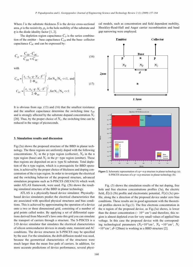
Fig.(2a) shows the proposed structure of the BBD in planar tech-nology. The three regions are uniformly doped with the following concentrations: NC in the p type region (collector), NB in the n type region (base) and NE in the p+ type region (emitter). These thee regions are deposited on an n- type Si substrate. Total deple-tion of the n type region, which is a prerequisite for BBD opera-tion, is achieved by the proper choice of thickness and doping con-centration of the n type region. In order to investigate the electrical and the switching behavior of the proposed structure, advanced simulation programs such as S-PISCES (SILVACO) which work under ATLAS framework, were used. Fig. (2b) shows the result-ing simulated structure of the BBD in planar technology.
ATLAS is a physically-based device simulator. Physically-based device simulators predict the electrical characteristics that are associated with specified physical structures and bias condi-tions. This is achieved by approximating the operation of a device onto a two or three dimensional grid, consisting of a number of grid points called nodes. By applying a set of differential equa-tions derived from Maxwell’s laws onto this grid you can simulate the transport of carriers through a structure. The S-PISCES is a 2-D device simulator that simulates the electrical characteristics of silicon semiconductor devices in steady-state, transient and AC conditions. The device structures in S-PISCES may be specified by the user. For the simulation, the drift-diffusion model was used, because the geometrical characteristics of the structures were much larger than the mean free path of carriers. In addition, for more accurate predictions of device performance, several physi-
cal models, such as concentration and field dependent mobility, Shockley-Read-Hall and Auger carrier recombination and band gap narrowing were employed.
Fig. (3) shows the simulation results of the net doping, free hole and free electron concentrations profiles (3a), the electric field, E(x) (3b) profile and electrostatic potential, V(x) (3c) pro-file, along the x direction of the proposed device under zero bias conditions. These results are in good agreement with the theoreti-cal profiles shown in Fig.(1). The free electrons concentration in the n region of the proposed device, as Fig.(3a) shows, is lower than the donor concentration (~ 1014 cm-3) and therefore, this re-gion is almost depleted even for very small values of applied bias voltage. In this case the proposed device with the correspond-ing technological parameters (NE=1019cm-3, NB =1017cm-3, NC =1016cm-3, d=120nm) is working as a BBD structure [2].
P. Papadopoulou and L. Georgopoulos /Journal of Engineering Science and Technology Review 2 (1) (2009) 157-164
Figure 2. Schematic representation of a p+-n-p structure in planar technology (a). S-PISCES structure of a p+-n-p structure in planar technology (b).

161
Figs. 4 (a and b) show the simulated I-V characteristics of the proposed BBD device in planar technology with NE=1019cm-3, NB =1017cm-3, NC =1016cm-3 and different middle region thicknesses d under forward and reverse bias conditions. The values of d were chosen to demonstrate the various operations of the devices. Thus for d=80nm, the I-V characteristics saturate even for low values of the applied voltage, because the structure in this case operates like p+- p junction [2]. I-V curves for d=150nm and 200nm indicate that the BBD operation begins at about 0.3V and 0.5V respectively. For voltages less than these values the current slightly increases with the voltage, because the free electron concentration in the middle region is very close to the donor concentration. Thus, a neutral zone appears in the middle region and the current is limited by a recombination mechanism. As the voltage increases the free
P. Papadopoulou and L. Georgopoulos /Journal of Engineering Science and Technology Review 2 (1) (2009) 157-164
Figure 3. S- PISCES data of net doping, free electron and hole concentrations (n(x), p(x)) (a), electric field E(x) (b) profile and electrostatic poten-tial V(x)(c) along the x(μm) direction along in the proposed BBD device under zero bias conditions.
Figure 4. S-PISCES data for Current – Voltage characteristics of the proposed BBD structure in planar technology with different d under forward (a) and reverse (b) bias conditions.

162
P. Papadopoulou and L. Georgopoulos /Journal of Engineering Science and Technology Review 2 (1) (2009) 157-164
electron density decreases exponentially, so that the neutral zone disappears and the current increases abruptly. For d=100nm and 120nm the structures operate as BBD’s for any forward bias volt-age applied, because the electron concentration in the middle layer is lower than the donor concentration and, therefore, this region is almost depleted even for very small values of applied bias voltage.
The reverse I-V characteristics are shown in Fig.4(b). For d=100nm and 120nm, the current rises with applied reverse bias voltage. For d=150nm and 200nm, the current rises slowly with the applied reverse bias voltage, because of the high free electron concentration in the middle layer and the formation of a neutral zone in this region. These simulated I-V characteristics of the pro-posed BBD structure in planar technology are in good agreement with the theoretical model.
In order to compare the two different design technologies, planar and non-planar, Figs. 5 (a, b) present the simulated I-V char-acteristics of BBD structures designed in non-planar technology,
Fig. 1(a). It is obvious that in Figs.4 (a, b) and Figs.5 (a, b) the same operation, for the different values of d is observed.
Figs. 6 (a, b) show the simulated I-V characteristics of the proposed BBD device in planar technology with NE=1019cm-3, NB =1017cm-3, d=100nm and different collector concentration NC (p type region), under forward and reverse bias conditions. Accord-ing to theoretical model, (Eqs. (5) and (7)) the barrier height in the forward ΦBR and reverse ΦBL bias conditions, are significantly influenced by the values of the NB and NC concentrations. Thus for large values of NC, the current increases in both bias condi-tions and goes into saturation even for low values of the applied voltage, because the corresponding barrier height ΦBR or ΦBL de-creases [2]. For lower values of NC the current takes lower values
Figure 5. S-PISCES data for Current – Voltage characteristics of a BBD struc-ture in no planar technology with different d under forward (a) and reverse (b) bias conditions.
Figure 6. S-PISCES data for Current – Voltage characteristics of the proposed BBD structure in planar technology with different collector concen-tration NC (p type region), under forward (a) and reverse (b) bias conditions.

163
and the corresponding devices are working as BBD structures.The proposed device in planar technology operates like BBD
devices designed in non-planar technology. As the proposed struc-tures designed in planar technology have the advantages of the BBD operation [1, 2], makes them attractive in applications such as gates in FETs or FinFETs, where current control is needed [22, 23].
The BBD structures as majority carrier devices, similar to Schottky diodes (i.e. not exhibiting minority carrier charge stor-age in the quasi-neutral regions) can be used for high-speed ap-plications, thus the switching behaviour of these structures was also investigated. More specifically, the influence of various tech-nological parameters on the switching behaviour of the proposed structure were investigated by means of simulation.
The simulation results of the collector current response when the applied bias switched between 1V to 0 V, is presented in Fig.7, for a structure with NE=1019cm-3, NB=1017cm-3 and d=120nm. It is obvious from this figure that when the bias voltage is switched from a forward voltage equal to 1V to zero voltage, the current through the structure changes abruptly from IF to a reverse current IR which afterwards decays exponentially to IS within a certain time. The switching time τSW for this structure is equal to 9.4 psec.
In Fig. 8, simulation results for the switching time τSW as a function of the middle region thickness d, is presented. In this case, the quantities NE, NB and NC were held constant. The ap-plied voltage was switched between forward and zero bias. As it can be seen from Fig. 8, τSW exhibits different dependences with respect to variable d similar to these observed for structures de-signed in no planar technology [20]. The switching time τSW ex-hibits a maximum. On the left and right of this maximum, τSW decreases and, finally on the right it saturates. The saturation on the right side is due to the saturation of the potential barrier ΦBL0.
In this case, a neutral zone is created in the base and the structure operates like a BJT [2]. As the middle region width decreases, ΦBL0 becomes gradually low and according to Eqs. (1) and (17), both capacitances CBC and CEB increase. Because the barrier is still relatively high, the dynamic resistance RD remains large and it does not affect significantly the total resistance of the device (“low injection” condition). Thus, τSW increases to, following the dependence of CBC on d. As d continues to decrease, the zero po-tential barriers become gradually lower and the corresponding current becomes larger. Gradually the device falls into the “high injection” condition, where RD becomes very small and it domi-nates in comparison with RS. In this region, the switching time fol-lows the dependence of RD which, according to the eqs. (1), (15) and (9), decreases by decreasing d. It is obvious that the maximum value of the switching time τSW is due to the “high” and “low” injection conditions.
Another significant technological parameter which affects the switching time of proposed BBD structures designed in planar tech-nology, is the collector dopand concentration NC (p type region). Fig. 9 shows the simulation results of τSW versus NC, for different structures with the same middle region thickness d (d=100nm). The applied voltage for all structures was switched between 1V and zero bias. It is obvious from Fig. 9 that τSW decreases by increasing the collector dopant concentration NC. Considering that the proposed structure with d=120nm operates in “low injection” conditions, the dominant resistance and capacitance in the transient process will be RS and CBC, respectively. Thus, according to Eqs. (14) and (17), the resulting time τSW should be inversely proportional to the square root of the substrate dopant concentration. Indeed Fig.9 shows that for large values of NC (i.e. for NC > 1015cm-3), τSW decreases linearly with a constant slope of -0.5 (on a log-log scale graph). For lower values of NC (i.e. for NC<1015cm3), the switching time τSW slightly changes, because as NC decreases, the depletion regions of the corresponding devices increase. Further increase of the depletion region is limited
Figure 7. Simulation results of the collector current response when the applied bias switched from 1V to 0 V, for a structure with NE = 1019cm-3, NB=1017cm-3, NC=1016cm-3 and d=120nm.
Figure 8. Influence of the middle layer thickness, d, on the total switching time τSW (data obtained from S- PISCES).
P. Papadopoulou and L. Georgopoulos /Journal of Engineering Science and Technology Review 2 (1) (2009) 157-164

164
by the geometry of the device. Finally, it is evident from Fig.9 that by the proper choice of the technological parameter NC, we can reduce switching time of the proposed structures in the picoseconds range (τSW ≈1 or 2 ps).
4. Conclusions
In this paper, we have proposed a p+-n-p structure designed in planar technology using simulation. We investigate the electrical and switching behavior of the proposed structures. The simulation results show that he proposed structure operates like a typical a
Bulk Barrier diode.More specifically, taking into consideration the electrical be-
havior, the main conclusion are:
• The barrier height is mainly a function of the NB, NC and of d; the limits of BBD operation can be controlled by the values of d and NB, for given values of NE and NC.
• The collector dopant concentration NC, strongly affects the current through the structure in both bias conditions.
• Barrier height engineering can easily be achieved by the ap-propriate choice of technological parameters.
Concerning the switching behavior, the main conclusion are:
• The proposed structures, as majority carrier devices, exhibit no minority carrier storage effect and, therefore, can operate with inherently fast response.
• The switching time of the proposed structure is mainly deter-mined by the depletion layer discharging time (τ ~ RC).
• The switching time is a function of the technological param-eters NB, NC and d and, thus, by the appropriate choice of these parameters, the switching time can reach the range of few picoseconds (τSW ≈1 or 2 ps).
As the proposed structures have the advantages of the BBD operation [2] and can be designed in planar technology, makes them attractive in many applications such as gates in FETs or Fin-FETs where current control is needed [22, 23] or as high speed devices in IC technology.
Acknowledgments
Research work supported by the Research and Fund Administra-tion Committee of Technological Education Institute of Kavala.
Figure 9. Influence of the collector dopant concentration, NC, on the total switching time, τSW, for different structures with d=100nm (data ob-tained from S- PISCES).
1. H. Mader, IEEE Trans. On Elect. Dev., ED-29 (11), 1766 (1982).2. P. Papadopoulou, N. Georgoulas, L. Georgopoulos and A. Thanailakis,
Electrical Engineering, Archiv für Elektrotechnik, 83(4), 203(2001).3. J. M. Shannon, App. Phys. Lett., 35, 63, (1979). 4. N. Georgoulas, IEEE Electron Device Lett., EDL-3, 61, (1982). 5. S. E. D. Habib and K. Board, IEEE Trans. On Elect. Dev., ED-30 (2), 86
(1983). 6. A. Al-Bustani, K. Board, IEE Proc. I, 134(1), 17, (1987). 7. A. Al-Bustani, IEE Proc. I, 134(4), 116, (1987). 8. S. E. D. Habib and K. Board, IEEE Trans. On Elect. Dev. ED-30 (2), 90,
(1983). 9. P. Papadopoulou, N. Georgoulas and A. Thanailakis, Thin Solid Film, 415,
276, (2002).10. H. Sakata, Y. Nagao and Y. Matsushima, Jour. of Cryst. Growth, 175-176,
Part 2, 1259 (1997). 11. P. Papadopoulou, N. Georgoulas, L. Magafas, Optoelectronics And Ad-
vanced Materials – Rapid Communications, 1 (8), 379, (2007).
12. Guo Der-Feng (1998): IEEE Journal of Quantum Electr., 34(10), 1882, (1998).
13. Guo Der-Feng, IEEE Journal Of Quantum Electronics, 40(4), 413, (2004).
14. Guo Der-Feng, IEEE Electron Device Letters, 27(1), 37, (2006).15. Guo Der-Feng, et al. Jour. of the Electrochemical Society, 154(1), H13,
(2007).16. Guo Der-Feng, et al., Surface Review and Letters, 15(1-2), 139, (2008).17. H. Schaffer, AEÜ 38, 69, (1984) 18. H. Mader, R. Müller, IEEE Trans. On Elect. Dev. ED-31(10), 1447,
(1984). 19. Wen-Shiung Lour (1997): Microel. Jour., 28 (5), 527 (1997). 20. P. Papadopoulou, et al., Microelectronics Journal, 33 (5-6), 487 (2002).21. Edward S Yang, Microelectronic Devices, McGRAW-HILL International
Editions, Electrical & Electronic Engineering Series, (1988). 22. Ki - Heung Park et al., IEEE Trans. On Nanotech., 7 (4), 427, (2008).23. A. Tsormpatzoglou et al. Solid State Electronics Article in Press.
References
P. Papadopoulou and L. Georgopoulos /Journal of Engineering Science and Technology Review 2 (1) (2009) 157-164