a study on electrical and magnetic characterization … thesis 2010 a study on electrical and...
TRANSCRIPT

Master Thesis
2010
A Study on Electrical and Magnetic Characterization of Co87Zr5Nb8 Films for
High-Q On-chip Inductors
Supervisor
Professor Nobuyuki Sugii
Professor Hiroshi Iwai
Department of Electronics and Applied Physics
Interdisciplinary Graduate School of Science and Engineering
Tokyo Institute of Technology
08M53403
Mokh. Sholihul Hadi

[2]
CONTENTS
Chapter 1
Introduction 4
1.1 Background of this study 5
1.2 On chip inductor 7
1.3 Soft Magnetic Material 8
1.4 Objective of this study 10
Chapter 2
Fabrication and Characterization Method 11
2.1 Experimental Procedure 12
2.1.1 Si Substrate Cleaning Process 12
2.1.2 Facing Target Sputtering 13
2.2 Measurement Methods 15
2.2.1 Scanning Electron Microscope (SEM) 15
2.2.2 Four-Point Probe Technique 17
2.2.3 Permeameter 20
2.2.4 Vibrating Sample Magnetometer 22
Chapter 3
Basic Magnetic Considerations of Soft Magnetic Material 25
3.1 B-H Loop Shape 26
3.2 Core Loss 27
[3]
3.3 Magnetic Anisotropy 29
3.4 Coercivity Field 31
3.5 Domain wall 35
3.6 Magnetostriction 38
3.7 Permeability 39
3.7.1 Relative permeability 42
3.7.2 Complex Permeability 42
Chapter 4
Result and Discussion 45
4.1 Resistivity 46
4.2 Film Structure Characterization 47
4.3 M-H Loop graph 48
4.4 Permeability 51
4.5 Core Loss 53
Chapter 5
Conclusions of This Study 54
5.1 Properties of Co87Zr5Nb8 55
5.2 Future Works 56
Reference 57
Acknowledgments 59

[4]
Chapter 1 Introduction
1.1 Background of This Study
1.2 On-chip inductor
1.3 Soft Magnetic Material
1.4 Objective of this study

[5]
1.1 Background of This Study
In recent years, power supply voltage for LSIs has been decreasing
year after year, as the result of CMOS downscaling. The power supply
voltage is now primarily at 0.9 – 1.2 V in the logic circuits. On the other
hand, the supply voltage from a rechargeable lithium-ion battery of 3.6 V is
mainly used for portable electronic equipments. Due to the increase of
difference between the battery voltage and LSI operating voltage,
high-efficiency voltage converter with reduced power loss have come to
attract widespread attention. So far, it has been investigated that series
regulator are replaced with switching dc–dc converters in many systems,
because the dc–dc converter has great advantage of efficiency in high
conversion ratio. But the conventional dc–dc converters are larger in size
than the series regulators. Therefore it is required to reduce their size and
thickness.
In order to shrink the size, the dc-dc converter should operate at
higher frequencies because passive elements can be smaller. Therefore, a
technology to fabricate passive elements that can be operated at high
frequencies is urgently needed. Most of dc-dc converters usually operate at
[6]
frequencies in the range of 100 kHz to 500 kHz, which are not suitable for
further reduction of the sizes of passive elements. High-Q on-chip inductor
has been a major challenge in the move towards in integrating the on-chip
dc-dc converter with high efficiency in a LSI chip. Most of on-chip
inductors in the literatures use a spiral geometry fabricated without
magnetic material and exhibit inductances ranging from 1 to 10 nH, but
consume large amount of area [5]. With the addition of magnetic material,
increased inductance L and quality factor Q with decreased capacitance,
resistance, and area can be achieved [1, 2, 4].
The on-chip inductor with magnetic material is needed to shrink its
dimension and to increase the inductance. The inductance however drops at
frequencies >100 MHz due to eddy currents circulating in the magnetic
film that generate resistive loss [1]. Considering a trade off between
dimension and inductance, a switching frequency range of 100 MHz to 500
MHz will be suited. One of the important properties of the magnetic thin
films required for such applications is their high-frequency properties. The
Co87Zr5Nb8 amorphous film has been considered as a candidate material
because amorphous magnetic material allows smaller, lighter and more

[7]
energy efficient designs in many high frequency applications compared to
nano-crystalline materials [3]. The coercivity and saturation magnetization
of the magnetic material are also important factors because they determine
the hysteretic loss and maximum eddy current.
1.2 On chip inductor
The on-chip inductors are commonly used for filter, amplifier, or
resonant circuits used in radio-frequency applications. The inductance have
typical values ranging from 1 to 100 nH, which give an equivalent
impedance between 10 and 1000 Ω, within the radio-frequency range at 300
MHz - 3 GHz (Figure 1.1). At frequencies lower than 100 kHz, discrete
inductors are used because of their high inductance values (From 1 to 100
µH) to keep the impedance between 10 and 1000 Ω. Such high inductances
cannot be integrated in a reasonable silicon area. Around 1 GHz, a 10 nH
on-chip inductor matches the standard 50 Ω impedance of most input and
output stages in very high frequency applications.

[8]
Figure 1-1. On-chip inductor with square model [14]
Figure 1-2. The inductor impedance versus frequency [14]
1.3 Soft Magnetic Material
Soft magnetic materials are essential constituents of nearly every
electrical device of modern civilization. So named because of the
correlation in ordinary steels between mechanical softness and ease of
magnetization reversal, soft magnetic materials perform the crucial task of

[9]
concentrating and shaping magnetic flux. The continuous development to
obtain better materials has resulted both in improved efficiencies of key
building blocks of present technologies: motors, generators, transformers,
inductors, and sensors in novel devices and applications.
It is widely recognized that most of the important properties for a
magnetic design engineer arise from a complex interplay between
fundamental properties controlled at the atomic level and the complex and
sophisticated processing used in the modern materials industry.
"Enlightened empiricism,"in the phrase of Gifkins, has been achieved
inspiration.
In this light, the development of soft magnetic materials has been
driven by the needs of design engineers. From the early days of this century,
research has been focused on simply stated goals: the desire for higher
permeability ρ, saturation induction , lower coercivity Hc, and core loss.
Improvements in these properties have resulted in power-handling
electrical devices with reduced size and weight and increased efficiency.

[10]
1.4 Objective of this study
This research presents a study on electrical and magnetic
characterization of Co87Zr5Nb8 films, which represent one of the desirable
promising amorphous magnetic material for proposed frequency range. The
magnetic material should have minimal hysteresis loss, high saturation
magnetization, low magnetostriction, high resistivity, and compatible with
Si technology.
[11]
Chapter 2
Fabrication and Characterization Method
2.1 Experimental Procedure
2.1.1 Si Substrate Cleaning Process
2.1.2 Facing Target Sputtering
2.2 Measurement Methods
2.2.1 Scanning Electron Microscope (SEM)
2.2.2 Four-Point Probe Technique
2.2.3 Permeameter
2.2.4 Vibrating Sample Magnetometer

[12]
2.1 Experimental Procedure
2.1.1 Si Substrate Cleaning Process
At first, high quality thin films require ultra clean Si surface without
particle contamination, metal contamination, organic contamination, ionic
contamination, water absorption, native oxide and atomic scale roughness.
One of the most important chemicals used in Si substrate cleaning is DI
(de-ionized) water. DI water is highly purified and filtered to remove all
traces of ionic, particulate, and bacterial contamination. The theoretical
resistivity of pure water is 18.25 MΩcm at 25oC. Ultra-pure water (UPW)
system used in this study provided UPW of more than 18.2 MΩcm at
resistivity, fewer than 1 colony of bacteria per milliliter and fewer than 1
particle per milliliter.
In this study, the Si substrate was cleaned on a basis of RCA cleaning
process. The first step, which uses a mixture of sulfuric acid (H2SO4) /
hydrogen peroxide (H2O2) (H2SO4: H2O2=4:1), was performed to remove
any organic material and metallic impurities. After that, the native or
chemical oxide was removed by diluted hydrofluoric acid (HF:H2O=1:99).
Then the cleaned wafer was dipped in DI water. Finally, the cleaned Si

[13]
substrate was loaded to the deposition chamber just after it was dried by air
gun.
2.1.2 Facing Target Sputtering
The amorphous Co87Zr5Nb8 alloy films were deposited on Si wafers
covered with a 400-nm thick SiO2 layer using a facing-target sputtering
apparatus at room temperature, resulting the introduction of in-plane
magnetic anisotropy, hard axis and easy Axis of magnetization, as shown in
Fig 2.1. Before the deposition, the chamber was evacuated to less than 8 x
10-7 Torr, and during the sputter deposition, the chamber was maintained at
0.25 mTorr, 0.5 mTorr, 0.75 mTorr, or 1 mTorr, using argon gas. A dc bias
of 50 V was applied to the substrate during the deposition. An external
magnetic field of ~35 Oe was applied to the substrates with permanent
magnets placed behind the facing targets. Figure 2.2 shows the facing
target sputtering apparatus chamber. Figure 2.3 shows the schematic
drawing of FTS vacuum chamber.

[14]
Figure 2.1. Fabrication and characterization of CoZrNb films
Figure 2.2. Facing Target Sputtering apparatus chamber

[15]
Figure 2.3.Schematic drawing of FTS vacuum chamber
2.2 Measurement Methods
2.2.1 Scanning Electron Microscope (SEM)
Figure 2.4 shows Scanning Electron Microscope (SEM) system. The
equipment is S-4800 (HITACHI High-Technologies Corporation).
Schematic drawing of electron beam system is shown in Fig. 2.5. The
‘Virtual Source’ at the top represents the electron gun, producing a stream
of monochromatic electrons. The stream is condensed by the first
condenser lens. This lens is used to both form the beam and limit the
amount of current in the beam. It works in conjunction with the condenser
aperture to eliminate the high-angle electrons into a thin, tight, coherent
beam. A user selectable objective aperture further eliminates high-angle

[16]
electrons from the beam. A set of coils then scan or sweep the beam in a
grid fashion and make the beam dwell on points for a period of time
determined by the scan speed. The final lens, the Objective, focuses the
scanning beam onto the part of the specimen desired. When the beam
strikes the sample, interactions occur inside the sample and are detected
with various instruments interactions. Before the beam moves to its next
dwell point these instruments count the number of interactions and display
a pixel on a CRT whose intensity is determined by this number. This
process is repeated until the grid scan is finished and then repeated, the
entire pattern can be scanned 30 times per second.
Figure 2.4 Photograph of SEM equipment.

[17]
Figure 2.5 Schematic drawings of SEM equipment.
2.2.2 Four-Point Probe Technique
The electrical resistivity was measured by using a conventional four
probe method. The four-point probe technique is one of the most common
methods for measuring the semiconductor resistivity because the
measured value by two-point probe includes parasitic effects. The sheet
resistance is calculated from potential difference between inside 2 terminals
(between B probe and C probe) after applying the current between outside

[18]
2 terminals (between A probe and D probe) as shown in fig. 2.5. The
resistance by two-probe technique is higher than accurate resistance
because it includes the contact resistance (RC) between metal probe and
semiconductor surface and spreading resistance (RSP) of each probe.
Neither RC nor RSP can be accurately calculated and thus semiconductor
resistance (RS) cannot be accurately extracted from the measured
resistance. On the other hand, four-probe technique can neglect these
parasitic resistances because the current which flows between the voltage
terminals is very small and potential drop can be disregarded. In this study,
sheet resistance was measured by four-probe technique. For an arbitrarily
shaped sample the sheet resistance (ρsh) is given by
ρsh=V/ I CF (2.1)
where CF is correction factor that depends on the sample geometry. If the
distance among probes (s; in this study, s=1 mm) is greatly shorter than the
width of a sample (d), CF equals to π/ln(2)=4.5

[19]
Fig 2.6. Illustration of four point probe system
Fig 2.7. Photograph of four point probe system

[20]
2.2.3 Permeameter
The hard-axis magnetic permeability was measured by using a
permeance meter with a frequency range from 1 MHz to 3 GHz. The
principle work of permeameter can be explained as follows, two electrical
inductors formed as primary and secondary concentric coils share a
common magnetic core space. An ac voltage applied to the primary coil
creates a magnetic flux in the core proportional to the magnetic
permeability of a sample of the material positioned within the core space.
The magnetic flux induces an ac voltage in the secondary coil indicative of
the sample magnetic permeability. When the material is a
magnetorheological fluid, the magnetic permeability is proportional to the
concentration of magnetic particles in the sample and can be
back-calculated from the amplitude of the secondary voltage signal.
Sensitivity and resolution can be increased by using two identical sets of
coils wherein a reference material forms a core for the primary set and the
MR fluid sample forms a core for the secondary set. Figure 2.8 shows
permeameter apparatus. Figure 2.9 shows the schematic drawings of
permeameter apparatus.

[21]
Fig 2.8. Photograph of permeameter
Figure 2.9 Schematic drawings of permeameter.

[22]
2.2.4 Vibrating Sample Magnetometer
Magnetic measurements of the films were performed with a vibrating
sample magnetometer (VSM) at room temperature. A sample is placed
inside a uniform magnetic field to magnetize the sample. The sample is
then physically vibrated sinusoidally, typically through the use of a
piezoelectric material. Commercial systems use linear attenuators of some
form and historically the development of these systems was done using
modified audio speakers, though this approached was dropped due to the
interference through the in-phase magnetic noise produced, as the magnetic
flux through a nearby pickup coil varies sinusoidally. The induced voltage
in the pickup coil is proportional to the sample's magnetic moment, but
does not depend on the strength of the applied magnetic field. In a typical
setup, the induced voltage is measured through the use of a lock-in
amplifier using the piezoelectric signal as its reference signal. By
measuring in the field of an external electromagnet, it is possible to obtain
the hysteresis curve of a material.
If a sample of any material is placed in a uniform magnetic field,
created between the poles of a electromagnet, a dipole moment will be

[23]
induced. If the sample vibrates with sinusoidal motion a sinusoidal
electrical signal can be induced in suitable placed pick-up coils. The signal
has the same frequency of vibration and its amplitude will be proportional
to the magnetic moment, amplitude, and relative position with respect to
the pick-up coils system. Fig. 2.8 shows the vibrating sample
magnetometer block diagram.
Fig. 2.8 Vibrating sample magnetometer block diagram.
The sample is fixed to a small sample holder located at the end of a sample
rod mounted in a electromechanical transducer. The transducer is driven by
a power amplifier which itself is driven by an oscillator at a frequency of
90 Hertz. So, the sample vibrates along the Z axis perpendicular to the

[24]
magnetizing field. The latter induced a signal in the pick-up coil system
that is fed to a differential amplifier. The output of the differential amplifier
is subsequently fed into a tuned amplifier and an internal lock-in amplifier
that receives a reference signal supplied by the oscillator. The output of this
lock-in amplifier, or the output of the magnetometer itself, is a dc signal
proportional to the magnetic moment of the sample being studied. The
electromechanical transducer can move along X, Y and Z directions in
order to find the saddle point (which Calibration of the vibrating sample
magnetometer is done by measuring the signal of a pure Ni standard of
known the saturation magnetic moment placed in the saddle point.
Fig 2.9. Photograph of vibrating sample magnetometer

[25]
Chapter 3 BASIC MAGNETIC
CONSIDERATIONS OF SOFT MAGNETIC MATERIAL
3.1. B-H Loop Shape
3.2 Core Loss
3.3 Magnetic Anisotropy
3.4 Coercivity Field
3.5 Domain wall
3.6 Magnetostriction
3.7 Permeability
3.7.1 Relative permeability
3.7.2 Complex Permeability
[26]
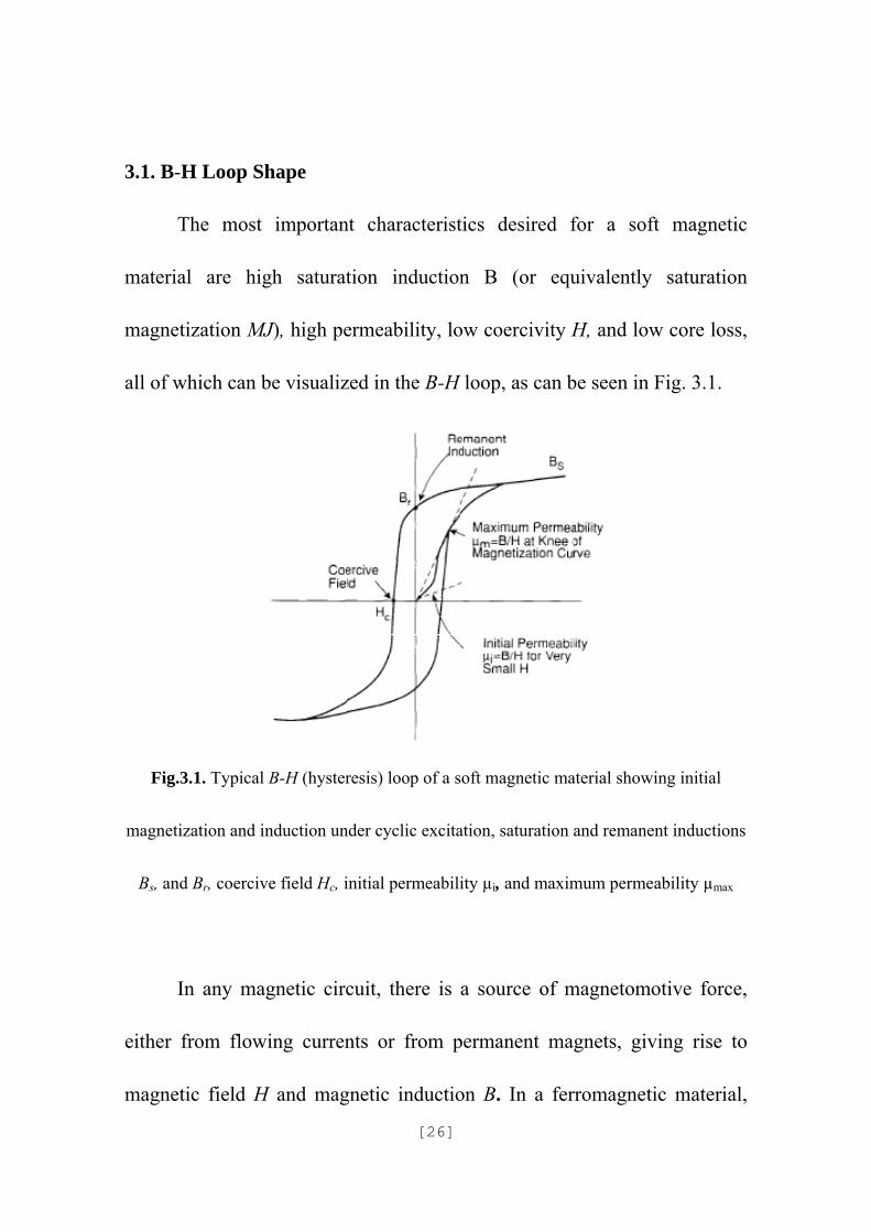
3.1. B-H Loop Shape
The most important characteristics desired for a soft magnetic
material are high saturation induction B (or equivalently saturation
magnetization MJ), high permeability, low coercivity H, and low core loss,
all of which can be visualized in the B-H loop, as can be seen in Fig. 3.1.
Fig.3.1. Typical B-H (hysteresis) loop of a soft magnetic material showing initial
magnetization and induction under cyclic excitation, saturation and remanent inductions
Bs, and Br, coercive field Hc, initial permeability µi, and maximum permeability µmax
In any magnetic circuit, there is a source of magnetomotive force,
either from flowing currents or from permanent magnets, giving rise to
magnetic field H and magnetic induction B. In a ferromagnetic material,

[27]
each magnetic atom carries a substantial magnetic moment which is
coupled by quantum mechanical exchange effects to the neighboring
moments. Below the Curie temperature Tc, the exchange energy is
sufficient to overcome thermal disorder, resulting in a finite spontaneous
magnetization. The total magnetization M is just the vector sum of the
moments of all individual atoms and B = µ0H + M, where µ0 is the
permeability of free space, 4πx 10-7 H/m in SI units. In a soft magnetic
material, M follows H readily, yielding relative permeabilities µ= B/µ0 H in
some cases 106 or larger. Magnetic materials also exhibit hysteresis, the
non-linear, non-local relationship between B and H, which is
parametrically displayed as the B-H loop. Soft and hard magnetic materials
have comparable saturation inductions, but are distinguished by their vastly
different coercivities: 0.2-100 A/m and 200-2000 kA/m, respectively, for
common commercial materials.
3.2 Core Loss
The best single measure of evolution of soft magnetic materials is the
reduction of core loss. Core losses in metallic magnetic materials are now
recognized to stem from the dissipation of the ohmic loss caused by

[28]
currents which are induced by changing flux in accordance with Faraday’s
law. The minimum possible loss per unit volume of a magnetic material is
the classical eddy current loss Pcl. For a strip material under sinusoidal flux
excitation:
P πB fh /6ρ 3.1
where B is maximum induction, f is frequency, ρ is electrical resistivity
and h is thickness. The classical loss presumes that B changes uniformly
through the cross-section of the sample. In practice, the total loss of any
real magnetic material is higher than Pcl,. The discrepancy arises from an
inevitable consequence of magnetic domain structure. In other than special
circumstances, the magnetic structure of a ferromagnet is characterized by
macroscopic regions called magnetic domains. Within each domain,
magnetization is essentially uniform in magnitude and direction; domain
walls provide the transition between these regions. The magnetization
process proceeds at least partially by motion of the walls. As H changes,
the dipolar energy E M.H dV is decreased by the growth of
domains in which M is favorably aligned with H at the expense of
anti-aligned domains. Hence, the total magnetization MVMdVincreases.

[29]
The discontinuous, spatially non-uniform nature of wall motion is
responsible for hysteresis and energy dissipation even under quasi-static
excitation and for the Barkhausen effect.
3.3 Magnetic Anisotropy
A key factor in our ability to tailor soft magnetic materials for a
broad spectrum of applications is an understanding of magnetic anisotropy
and how a control by a choice of composition and thermomechanical
processing. Magnetic anisotropy is the tendency of the magnetization
vector within a piece of magnetic material to be aligned in a particular
direction called the easy axis of magnetization. In an actual sample, the net
direction of the magnetization is determined by a competition among the
dipolar energy Ed and the various sources of anisotropy, principally
magnetocrystalline anisotropy, stress anisotropy, induced uniaxial
anisotropy, and shape anisotropy.
When a material is magnetized along its easy axis, permeability is
high and saturation is easily achieved; in a hard direction, a field
H 2π/M , (the anisotropy field) is needed to rotate the magnetization

[30]
direction in the presence of an anisotropy energy density K, see fig. 3.2.
Anisotropy is important even for easy-axis magnetization: in the simplest
approximation the initial permeability µ 1K while the approach to
saturation always involves rotational magnetization of at least some closure
domain regions.
In the language of quantum mechanics, each magnetic atom carries
both spin (S) and orbital (L) angular momentum. Each of the magnetic
electrons' eigenstates has a particular spatial charge distribution which
interacts electrostatically with the crystal field produced by the charge
cloud surrounding the neighboring atoms. Those magnetic wavefunctions
which minimize the electrostatic interaction are energetically favored. The
symmetry of the crystal field and the allowed magnetic electron
wavefunctions establish the easy axis of magnetization. With uniaxial
symmetry the anisotropy has a functional form with leading term
K K sin θ, where θ is the angle between M and the easy axis. In a
cubic

[31]
Fig. 3.2. Schematic B-H loops with magnetization
along the easy and hard axis of magnetization.
system, K 0 and a much weaker term K l m m n n l ,
where l, m, and n are the direction cosines of M, normally dominates.
Depending on the sign of K1, for example either the [001] (α-Fe) or [111]
(α-Ni) direction may be the easy axis. The magnitude of the anisotropy
energy varies widely. The crystal field acts directly on L but only indirectly
on S through spin-orbit coupling L.S.
3.4 Coercivity Field
Coercivity or coercive field, of a ferromagnetic material is the
intensity of the applied magnetic field required to reduce the magnetization
[32]
of that material to zero after the magnetization of the sample has been driven
to saturation. Coercivity is usually measured in Oe or A/m units and is
denoted HC.
Materials with high coercivity are called as hard ferromagnetic
materials, and are utilized for permanent magnets. Permanent magnets find
application in electric motors, magnetic recording media and magnetic
separation. A material with a low coercivity is said to be soft and may be
used in microwave devices, magnetic shielding, transformers, or recording
heads.
Typically the coercivity of a magnetic material is determined by
measurement of the hysteresis loop or magnetization curve. The apparatus
used for the measurement is typically a vibrating-sample or
alternating-gradient magnetometer. The applied field where the
magnetization crosses to zero is the coercivity. If an antiferromagnet is
present in the sample, the coercivities measured in increasing and decreasing
fields may be unequal as a result of the exchange bias effect.

[33]
The coercivity of a material depends on the time scale over which a
magnetization curve is measured. The magnetization of a material
measured at an applied reversed field which is nominally smaller than the
coercivity may, over a long time scale, slowly creep to zero. Creep occurs
when reversal of magnetization by domain wall motion is thermally
activated and is dominated by magnetic viscosity. The increasing value of
coercivity at high frequencies is a serious obstacle to the increase of data
rates in high-bandwidth magnetic recording, compounded by the fact that
increased storage density typically requires a higher coercivity in the
media.
At the coercive field, the vector component of the magnetization of a
ferromagnet measured along the applied field direction is zero. There are
two primary modes of magnetization reversal: rotation and domain wall
motion. When the magnetization of a material reverses by rotation, the
magnetization component along the applied field is zero because the vector
points in a direction orthogonal to the applied field. When the magnetization
reverses by domain wall motion, the net magnetization is small in every
vector direction because the moments of all the individual domains sum to

[34]
zero. Magnetization curves dominated by rotation and magnetocrystalline
anisotropy are found in relatively perfect magnetic materials used in
fundamental research. Domain wall motion is a more important reversal
mechanism in real engineering materials since defects like grain boundaries
and impurities serve as nucleation sites for reversed-magnetization domains.
The role of domain walls in determining coercivity is complex since defects
may pin domain walls in addition to nucleating them.
As with any hysteretic process, the area inside the magnetization
curve during one cycle is work that is performed on the magnet. Common
dissipative processes in magnetic materials include magnetostriction and
domain wall motion. The coercivity is a measure of the degree of magnetic
hysteresis and therefore characterizes the lossiness of soft magnetic
materials for their common applications.
The squareness (M(H=0)/Ms) and coercivity are figures of merit for
hard magnets although energy product (saturation magnetization times
coercivity) is most commonly quoted. The 1980s saw the development of
rare earth boride magnets with high energy products but undesirably low

[35]
Curie temperatures. Since the 1990s new exchange spring hard magnets with
high coercivities have been developed.
3.5 Domain wall
In magnetism, a domain wall is an interface separating magnetic
domains. It is a transition between different magnetic moments and usually
undergoes an angular displacement of 90° or 180°. Domain wall is a gradual
reorientation of individual moments across a finite distance. The domain
wall thickness depends on the anisotropy of the material, but on average
spans across around 100-150 atomic radii.
The energy of a domain wall is simply the difference between the
magnetic moments before and after the domain wall was created. This value
is usually expressed as energy per unit wall area.

Fig
that
ener
favo
indiv
redu
redu
thus
anti-
3.3 Domain
The wid
create it:
rgy (Jex), b
orable ene
vidual ma
ucing the
uced when
s makes th
-parallel a
n wall (B) w
tw
dth of the
the Magn
both of wh
ergetic st
agnetic mo
width of
n the magn
he wall th
alignment
with gradual
wo 180-deg
domain w
netocrysta
hich want t
tate. The
oments ar
the doma
netic mom
hicker, du
would bri
[36]
l re-orientat
gree domain
wall varies
alline anis
to be as low
anisotrop
re aligned
ain wall. W
ments are a
ue to the r
ng them c
tion of the m
ns (A) and (C
s due to the
sotropy en
w as possi
py energy
with the
Whereas t
aligned pa
repulsion
closer - wo
magnetic mo
C)
e two opp
nergy and
ible so as t
y is low
crystal lat
the excha
arallel to e
between
orking to r
oments betw
osing ener
the exch
to be in a m
est when
ttice axes
ange energ
each other
them. (W
reduce the
ween
rgies
ange
more
n the
thus
gy is
r and
Where
wall
[37]
thickness.) In the end an equilibrium is reached between the two and the
domain wall's width is set as such.
An ideal domain wall would be fully independent of position,
however in the actual material, the domain wall get stuck on inclusion sites
within the medium, known as crystallographic defects. These include
vacancies, interstitials, dislocations, or different atoms, oxides, insulators
and even stresses within the crystal. This prevents the formation of domain
walls and also inhibits their propagation through the medium. Thus a greater
applied magnetic field is required to overcome these sites.
Non-magnetic inclusions in the volume of a ferromagnetic material,
or dislocations in crystallographic structure, can cause "pinning" of the
domain walls. Such pinning sites cause the domain wall to seat in a local
energy minimum and external field is required to "unpin" the domain wall
from its pinned position. The act of unpinning will cause sudden movement
of the domain wall and sudden change of the volume of both neighbouring
domains. This causes Barkhausen noise and in effect it is most likely to be
the source of magnetic hysteresis.

[38]
3.6 Magnetostriction
Magnetostriction is a property of ferromagnetic materials that causes
them to change their shape or dimensions during the process of
magnetization. The variation of material's magnetization due to the applied
magnetic field changes the magnetostrictive strain until reaching its
saturation value, λ. The effect was first identified in 1842 by James Joule
when observing a sample of nickel. This effect can cause losses due to
frictional heating in susceptible ferromagnetic cores.
The reciprocal effect, the change of the susceptibility of a material
when subjected to a mechanical stress, is called the Villari effect. Two other
effects are thus related to magnetostriction: the Matteucci effect is the
creation of a helical anisotropy of the susceptibility of a magnetostrictive
material when subjected to a torque and the Wiedemann effect is the twisting
of these materials when a helical magnetic field is applied to them. The
Villari Reversal is the change in sign of the magnetostriction of iron from
positive to negative when exposed to magnetic fields of approximately 40 k

[39]
A/m (500 Oe). On magnitude of the magnetostriction, change in volume by
applying magnetic field are small: the order of ~10-6.
3.7 Permeability
In electromagnetism, permeability is the measure of the ability of a
material to support the formation of a magnetic field within itself. In other
words, it is the degree of magnetization that a material obtains in response to
an applied magnetic field. Magnetic permeability is typically represented by
the Greek letter μ. The term was coined in September 1885 by Oliver
Heaviside. The reciprocal of magnetic permeability is magnetic reluctivity.
In SI units, permeability is measured in H/m, or N/A2. The
permeability constant (μ0), also known as the magnetic constant or the
permeability of free space, is a unit of the amount of resistance encountered
when forming a magnetic field in vacuum. The magnetic constant is defined
to be value of µ0 = 4π×10−7 ≈ 1.2566370614...×10−6 H·m-1 or N·A-2).
In electromagnetism, the auxiliary magnetic field H represents how a
magnetic field B influences the organization of magnetic dipoles in a given

[40]
medium, including dipole migration and magnetic dipole reorientation. Its
relation to permeability is
B µH 3.2
where the permeability μ is a scalar if the medium is isotropic or a second
rank tensor for an anisotropic medium.
In general, permeability is not a constant, as it can vary with the
position in the medium, the frequency of the field applied, humidity,
temperature, and other parameters. In a nonlinear medium, the permeability
can depend on the strength of the magnetic field. Permeability as a function
of frequency can take on real or complex values. In ferromagnetic materials,
the relationship between B and H exhibits both non-linearity and hysteresis:
B is not a single-valued function of H, but depends also on the history of the
material.
Permeability is the inductance per unit length. In SI units,
permeability is measured in H/m = J/(A2·m) = N/A). The auxiliary magnetic
field H has dimensions current per unit length and is measured in units of

[41]
A/m. The product μH thus has dimensions inductance times current per unit
area (H·A/m2). But inductance is magnetic flux per unit current, so the
product has dimensions magnetic flux per unit area. This is just the magnetic
field B, which is measured in Wb/m2 ,V·s/m2, T.
B is related to the Lorentz force on a moving charge q:
. F q E v V 3.3
The charge q is given in C, the velocity v in m/s, so that the force F is in N:
qv B C · · V.C. J C J N 3.4
H is related to the magnetic dipole density. A magnetic dipole is a closed
circulation of electric current. The dipole moment has dimensions current
times area, units A·m2, and magnitude equal to the current around the loop
times the area of the loop. The H field at a distance from a dipole has
magnitude proportional to the dipole moment divided by distance cubed,
which has dimensions current per unit length.

3.7.
Rela
the p
by th
In te
χm,
susc
susc
3.7.2
com
mag
each
1 Relative
ative perm
permeabil
he magnet
µ µµ
erms of re
χm =
a dimens
ceptibility,
ceptibility)
2 Complex
A usefu
mplex perm
gnetic field
h other th
e permeab
meability,
ity of a sp
tic constan
lative perm
μr − 1.
sionless q
, to disti
) and χM (m
x Permeab
ul tool for
meability.
d and the
hrough so
ility
sometime
ecific med
nt
meability,
.
quantity,
inguish i
molar or m
bility
r dealing w
While at
auxiliary
ome scalar
[42]
es denoted
dium to th
, the magn
is someti
it from χ
molar mas
with high
t low freq
magnetic
r permeab
d by the sy
he permeab
:
netic susce
imes call
χp (magn
ss suscepti
frequency
quencies i
c field are
bility, at
ymbol μr,
bility of fr
eptibility i
ed volum
netic mass
ibility).
y magnetic
in a linea
e simply p
high freq
is the rati
ee space g
is:
metric or
s or spe
c effects i
ar material
proportion
quencies t
io of
given
3.5
3.6
bulk
ecific
s the
l the
nal to
these

[43]
quantities will react to each other with some lag time. These fields can be
written as phasors, such that:
H H e 3.7
B B e 3.8
where δ is the phase delay of B from H. Understanding permeability as the
ratio of the magnetic field to the auxiliary magnetic field, the ratio of the
phasors can be written and simplified as
μ BH
B ω δ
H ωBHe δ, 3.9
so that the permeability becomes a complex number. By Euler's formula, the
complex permeability can be translated from polar to rectangular form,
µ BHcosδ j B
Hsinδ µ jµ" 3.10
The ratio of the imaginary to the real part of the complex permeability is
called the loss tangent,
tanδ µ"
µ" 3.11

[44]
which provides a measure of how much power is lost in a material versus
how much is stored.

[45]
Chapter 4
Result and Discussion 4.1 Resistivity
4.2 Film Structure Characterization
4.3 M-H Loop graph
4.4 Permeability
4.5 Core Loss

4.1 R
prob
sam
the
thick
µΩ-
resis
resis
ferro
valu
Resistivit
The ele
be method
mples with
ρ are ha
kness. The
-cm. This
stivity val
stivity val
omagnetic
ue of ele
Figur
y
ectrical res
d. Figure
different
ardly dep
e resistivit
value is m
ue of 20 µ
lue is ver
c resonanc
ctrical res
re 4.1. R
diffe
sistivity w
4.1 show
thickness
pendent on
ty of The
much high
µΩ-cm, an
ry importa
ce of frequ
sistivity is
Resistivity
erent thick
[46]
was measu
ws the ele
s and arg
n the de
Co87Zr5N
her than N
nd 100 µΩ
ant, that w
uency mor
better.
y of Co
kness and a
ured by us
ectrical re
gon gas p
position
Nb8 sample
NiFe and C
Ω-cm, resp
will reduc
re that 100
o87Zr5Nb8
argon gas
sing a con
esistivity o
pressure. It
gas press
s has resis
CoZrTa [2
pectively.
ce eddy c
0 MHz.
samples
pressure
nventional
of Co87Zr
t is notice
sure and
stivity of ~
2] which
The elect
currents a
So that hi
s with
four
r5Nb8
eable
film
~120
have
trical
nd a
igher

4.2 F
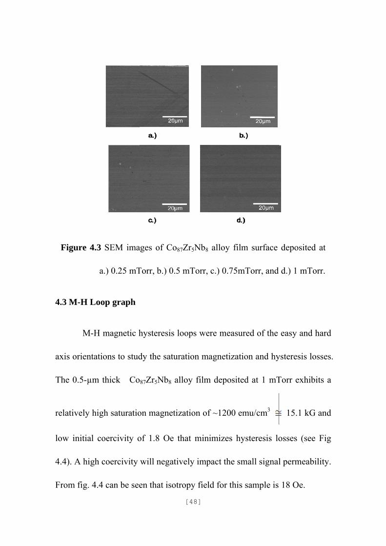
Scan
film
Co87
A
the
Co87
0.75
pres
Film Stru
Film
nning Elec
m thickness
7Zr5Nb8 al
Figu
A SiO2 film
proposed
7Zr5Nb8 a
5mTorr, a
ssure cond
ucture Ch
texture a
ctron Mic
s. Figure 4
lloy film d
ure 4.2. C
Co8
m was cho
on-chip
alloy film
and 1 mT
ditions are
haracteriz
and surfac
croscope (
4.2 shows
deposited
Cross-secti
87Zr5Nb8 a
osen as a i
inductor.
m surface
Torr. All
quite the
[47]
zation
ce morph
SEM). SE
s cross-sec
at 1 mTor
ional SEM
alloy film
nsulator, t
Fig. 4.3
e deposite
the surf
same.
hology we
EM was al
ctional SE
rr.
M images
deposited
that is the
shows p
ed at 0.2
face morp
ere observ
lso used t
EM image
of 1-µm
d at 1 mTo
e same lay
planar SE
25 mTorr
phologies
ved by u
to measure
of 1-µm t
thick
rr
yer structu
EM image
r, 0.5 mT
at these
using
e the
thick
re as
es of
Torr,
gas
Fig
4.3 M
axis
The
relat
low
4.4)
From
gure 4.3
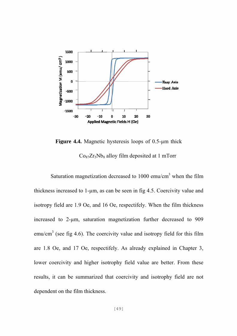
a.
M-H Loo
M-H m
orientatio
0.5-µm t
tively high
initial co
. A high c
m fig. 4.4
SEM ima
.) 0.25 mT
p graph
magnetic h
ons to stud
thick Co
h saturatio
oercivity o
coercivity
can be see
ages of Co
Torr, b.) 0.
hysteresis
dy the satu
o87Zr5Nb8
on magnet
of 1.8 Oe
will negat
en that iso
[48]
o87Zr5Nb8
.5 mTorr,
loops we
uration ma
alloy film
tization of
that mini
tively imp
otropy fiel
alloy film
c.) 0.75m
ere measur
agnetizatio
m deposite
f ~1200 em
imizes hy
pact the sm
ld for this
m surface
mTorr, and
red of the
on and hy
d at 1 mT
mu/cm3
ysteresis lo
mall signal
sample is
deposited
d.) 1 mTo
easy and
ysteresis lo
Torr exhib
15.1 kG
osses (see
l permeab
18 Oe.
d at
orr.
hard
osses.
bits a
G and
e Fig
ility.
thick
isotr
incre
emu
are
lowe
resu
depe
Satura
kness incr
ropy field
eased to
u/cm3 (see
1.8 Oe, a
er coerciv
ults, it can
endent on
Figu
ation magn
reased to 1
are 1.9 O
2-µm, sa
fig 4.6).
and 17 Oe
vity and h
n be summ
the film th
ure 4.4. M
Co
netization
1-µm, as c
Oe, and 16
aturation
The coerc
e, respect
higher iso
marized th
hickness.
Magnetic h
87Zr5Nb8 a
[49]
decreased
can be see
6 Oe, resp
magnetiz
civity valu
ifely. As
otrophy fie
hat coerci
hysteresis
alloy film
d to 1000
en in fig 4
ectifely. W
zation furt
ue and iso
already e
eld value
ivity and
s loops of
deposited
emu/cm3
.5. Coerci
When the
ther decr
otropy fiel
explained
are bette
isotrophy
f 0.5-µm t
d at 1 mTo
when the
ivity value
film thick
reased to
ld for this
in Chapte
er. From t
y field are
thick
orr
film
e and
kness
909
film
er 3,
these
e not

Figu
Fig
ure 4.5. M
Co
gure 4.6 M
Co
Magnetic
o87Zr5Nb8 a
Magnetic
o87Zr5Nb8
[50]
hysteresi
alloy film
hysteresis
alloy film
is loops o
deposited
s loops o
m deposite
of 1-µm t
d at 1 mTo
f 2-µm th
d at 1 mT
thick
orr
hick
orr

[51]
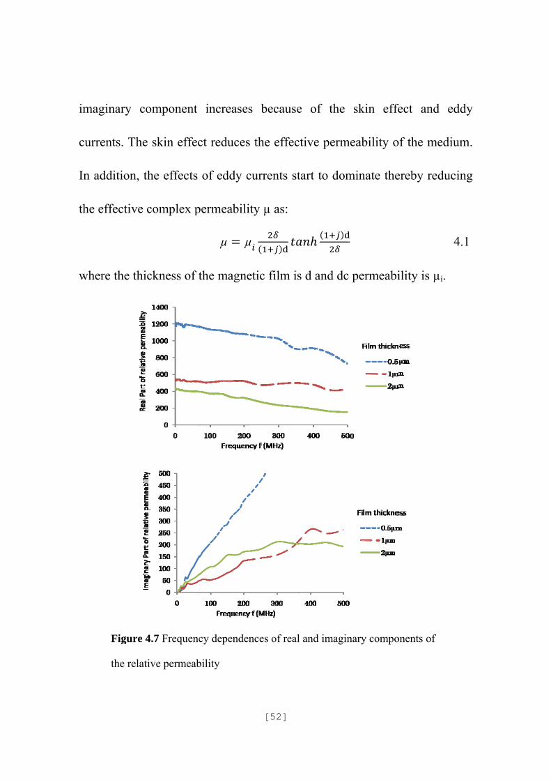
The magnetic properties of Co87Zr5Nb8 alloy films were summarized
in Table 4.1. It is noticeable the value of Hc, Hk, are hardly dependent on
the deposition gas pressure and film thickness.
4.3 Permeability
The small signal permeability as a function of frequency up to 500
MHz was measured, as can be seen in Fig 4.7. As the film thicknesses
increases, the real component of the permeability decreases and the
Table 4.1. Properties of Co87Zr5Nb8
Thickness
(µm)
Pressure during
deposition
(mTorr)
Ms
(emu/cm3)
Hce
(Oe)
Hch
(Oe)
Hk
(Oe)
1.0 0.25 812 2.0 1.8 17
18
16
16
16
17
18
17
1.0 0.50 925 4.5 2.0
1.0 0.75 894 3.5 1.5
1.0 1.0 1000 2.4 1.9
2.0 0.25 816 3.3 1.6
2.0 0.50 925 4.5 1.8
2.0 0.75 1000 1.6 1.5
2.0 1.0 909 1.8 1.9
imag
curr
In a
the e
whe
ginary co
rents. The
ddition, th
effective c
ere the thic
Figure 4
the relati
omponent
skin effec
he effects
complex p
ckness of t
4.7 Frequenc
ive permeab
increases
ct reduces
of eddy c
permeabili
µ µ
the magne
cy dependen
bility
[52]
s because
s the effec
currents st
ity µ as:
µ
etic film is
nces of real
e of the
ctive perm
tart to dom
s d and dc
l and imagin
skin effe
meability o
minate the
permeabi
nary compo
fect and e
of the med
ereby redu
ility is µi.
onents of
eddy
dium.
ucing
4.1
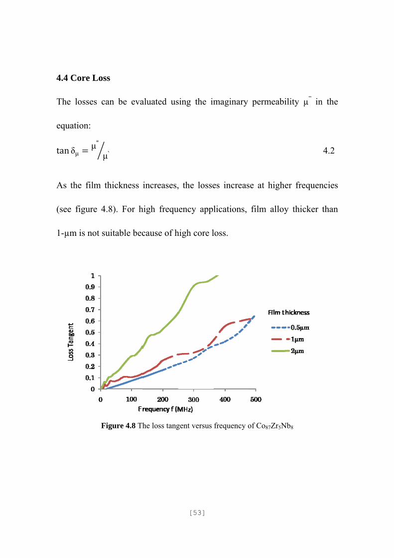
4.4 C
The
equa
tan δ
As t
(see
1-µm
Core Los
losses ca
ation:
δμμ"
μ
the film t
figure 4.
m is not su
Fi
s
an be eva
μ`
thickness
.8). For h
uitable bec
igure 4.8 Th
aluated us
increases,
high frequ
cause of h
he loss tang
[53]
sing the im
, the losse
uency appl
high core l
gent versus
maginary
es increas
lications,
loss.
frequency o
permeabi
se at highe
film alloy
of Co87Zr5N
ility µ” in
er frequen
y thicker
Nb8
n the
4.2
ncies
than

[54]
Chapter 5 Conclusions of This Study
5.1 Properties of Co87Zr5Nb8
5.2 Future Works

[55]
5.1 Properties of Co87Zr5Nb8
Electrical and magnetic properties of the amorphous Co87Zr5Nb8
films were examined. The Co87Zr5Nb8 alloy film deposited at 1 mTorr
exhibits a relatively high saturation magnetization of ~1200 emu/cm3
15.1 kG and low initial coercivity of 1.8 Oe that minimizes hysteresis
losses. Coercivity (~2 Oe), anisotropy field (~17 Oe), resistivity (~120
Ωcm) did not depend on the deposition conditions and thickness up to 2 µm.
Co87Zr5Nb8 has ferromagnetic resonance of 1.3 GHz. The 0.5-µm thick
Co87Zr5Nb8 alloy film deposited at 1 mTorr exhibits ~1200 real part
permeability up to 500 MHz. Core loss performance of Co87Zr5Nb8 alloy
film thinner than 1µm shows good properties up to 500 MHz. The current
results show that Co87Zr5Nb8 is a suitable magnetic material for the
proposed on-chip inductor with switching frequency range up to 500 MHz.
Co87Zr5Nb8 is rated as good soft magnetic alloy for the proposed
on-chip inductors because of its good combination of magnetic properties.
High saturation magnetization and low coercivity of the magnetic material

are
dete
5.2 F
usin
1-µm
vario
show
effic
indu
of C
struc
important
ermine the
Future w
In the n
ng Co87Zr5
m, 0.5-µm
ous ways
wn in Fig
cient meth
uctor perfo
Co87Zr5Nb
cture will
Fig 5.1
t because
e hysteretic
orks
next step,
5Nb8 as m
m or thinne
to integr
gure 5.1.
hod to red
ormance c
8 magnetic
be conduc
various wa
they will
c losses.
, fabricati
magnetic fi
er Co87Zr5
rate magn
In Figure
duce the m
compared
c film laye
cted.
ay to integra
[56]
l limit the
on of on-
ilm layer.
5Nb8 film
netic mate
e 5.1, the
magnetic
with othe
er insertio
ate magnetic
e maximu
-chip indu
Consider
alloys wil
erials into
sandwich
energy le
er ways. In
on into on-
c film into o
um curren
uctor will
r to the re
ll be suite
inductor
h structur
eak and to
n the next
-chip indu
on-chip indu
nt density
be condu
esearch re
ed. There
structure
re is the m
o increase
t step, A s
uctor sandw
ductor struct
and
ucted
esult,
e are
s, as
most
e the
study
wich
ture.
[57]
References
[1] D. S. Gardner, G. Schrom, P. Hazucha, F. Paillet, T. Karnik and S.
Borkaret, IEEE Trans. Magn., vol.43, no.6, pp.2615-2617, June
(2007).
[2] D. S. Gardner, G. Schrom, P. Hazucha, F. Paillet, T. Karnik, S.
Borkaret, R. Hallstein, T. Dambrauskas, C. Hill, C. Linde, W.
Worwag, R. Baresel, and S. Muthukumar, J. Appl.Phys., 103,
07E927 (2008).
[3] M. Yamaguchi, J. Appl. Phys., vol. 85, no. 11, pp. 7919-7922,
(1999).
[4] S. S. Mohan, M. Hershenson, S.P. Boyd, and T. H. Lee, IEEE J.
Solid State Circuits, vol. 34, no. 10, pp. 1419-1424, Oct (1999).
[5] G. E. Fish, IEEE. Vol. 78, no. 6, June (1990)
[6] Ito T. et. al., J. Magn. Soc. Japan, 28, 401, (2004)
[7] J. Michel, Y. Lamy, A. Royet, and B. Viala, in Proc. Int. Magn., p.
57, (2007).
[8] A. Crawford, D. S. Gardner, and S. Wang, IEEE Trans. Magn., vol.
40, no. 4, pp. 2017–2019, Jul. (2004).
[9] M.E. McHenry, M. A. Willard, D. E. Laughlin. Progress in
Materials Science, vol. 44, pp. 291-433, (1999).
[10] J. Salvia, J. A. Bain, and C. P. Yue, Proc. IEEE IEDM, pp. 943–946,
(2005).

[58]
[11] M. Yamaguchi, M. Baba, and K. I. Arai, T. Microwave Theory, vol.
49, no. 12, pp. 2331–2335, (2001).
[12] V. Korenivski, R. B. Van Dover. IEEE Trans. Mag., 34., pp. 1375,
(1998).
[13] T. Sato, H. Tomita, A. Sawabe, T. Inoue, T. Mizoguchi, M. Sahashi:
IEEE Trans. Mag., vol. 30, pp. 217, (1994).
[14] M. H. Park, Y. K. Hong, S. H. Gee, M. L. Mottern, T. W. Jang, S.
Burkett, J. Appl. Phys., vol. 91, pp. 7218, (2002).
[15] N. X. Sun, S. X. Wang, J. Appl. Phys., vol. 92, pp. 1477, (2002).
[59]
Acknowledgments I would like to thank my academic supervisor Professor Nobuyuki Sugii,
and Professor Hiroshi Iwai for their excellent guidance and continuous
encouragement, as well as financial support of the project. I am great
thanks to Associate Professor Yoshitaka Kitamoto from Department of
Innovative and Engineered Material for his supervision on my research. I
am deeply thanks to Assistant Professor Kuniyuki Kakushima for his
continuous supports.
I would also like to express gratitude to Professor Takeo Hattori,
Professor Kenji Natori, Professor Akira Nishiyama, Professor Kazuo
Tsutsui, and Associate Professor Parhat Ahmet for for many useful advices.
Thanks to Prof. Shigeki Nakagawa from graduate school of science and
engineering Tokyo Institute of Technology, and Prof. Nobuhiro Matsushita
from interdisciplinary graduate school of science and engineering, Tokyo
Institute of Technology for their support.
Thanks to all Iwai Laboratory member for their kind friendship. I
would like to express sincere gratitude to laboratory secretaries, Ms. A.
Matsumoto, Ms. M. Karakawa, and Ms. M. Nishizawa. Thanks to
Indonesia Ministry of Education for providing DIKTI scholarship.
Finally, I would like to thank my family for their endless love and
support.
July 2010
Mokh. Sholihul Hadi