a survey of clock distribution techniques including optical and rf
TRANSCRIPT

A Survey of Clock Distribution Techniques Including Optical and RF Networks
by
Sachin Chandran
A report submitted to the Graduate Faculty ofAuburn University
in partial fulfillment of therequirements for the Degree of
Master of Electrical Engineering
Auburn, AlabamaDecember 14, 2013
Keywords: Clock distribution networks, clock trees, clock skew, clock jitter, H-trees,optical clock, RF clock, wireless clock
Copyright 2013 by Sachin Chandran
Approved by
Vishwani Agrawal, Chair, James J. Danaher Professor of Electrical and ComputerEngineering
Victor Nelson, Professor of Electrical and Computer EngineeringAdit Singh, James B. Davis Professor of Electrical and Computer Engineering

Abstract
Clock distribution has become an increasingly challenging problem for VLSI designs,
consuming an increasing fraction of resources such as wiring, power, and design time. Power
consumption of up to 40% - 50% has been reported on clock distribution. Unwanted dif-
ferences or uncertainties in clock network delays degrade performance or cause functional
errors. Although there are lots of other techniques and research in clock distribution net-
works, in this report a detailed study of wireless and optical clock distributions is performed
and compared with the conventional clock distribution technique. These techniques employ
either transmitter/receiver or optical fiber to distribute clock signal to entire chip, so that
there is a reduction in interconnecting wires which reduces the total load capacitance of the
clock distribution network. Finally some future work is discussed on these techniques.
ii

Acknowledgments
I would like to express my gratitude to people who helped me complete this project.
First, I must thank my advisor Dr. Vishwani Agrawal who lent me so much help during
the course of the project. When I met with problems, he would guide me to solve those
problems, either through emails or face to face meetings.
I am also deeply grateful to my committee members, Dr. Adit Singh and Dr. Victor
Nelson for their valuable courses and project which were extremely useful in understanding
the core concepts in VLSI.
I must thank my parents Anusha and Chandran for their love, prayers, and support and
giving me everything more than what they had. I am grately indebted to my brother Sajan
Chandran, without whom I would not have pursued my graduate studies. I would like to
thank my manager Xin Ma, Intel, Hudson, MA for giving me an opportunity to work on
the Haswell Server microprocessor clock distribution team, where I worked on building clock
spines and also calculate the load on the clock network. I also want to thank my manager
Bill Maghielse, ARM Inc, Austin, TX for giving me an opportunity to work on the gate
level simulation for ATLAS 64-bit microprocessor and minimize power in decode stage of
the pipeline using various techniques. Finally and most importantly, I must thank God for
sustaining me each and every day and for being my ultimate source of strength, renewal,
and hope.
iii
Table of Contents
Abstract . . . . . . . . . . . . . . . . . . . . . . . . . . . . . . . . . . . . . . . . . . . ii
Acknowledgments . . . . . . . . . . . . . . . . . . . . . . . . . . . . . . . . . . . . . . iii
List of Figures . . . . . . . . . . . . . . . . . . . . . . . . . . . . . . . . . . . . . . . vi
List of Tables . . . . . . . . . . . . . . . . . . . . . . . . . . . . . . . . . . . . . . . . viii
1 Introduction . . . . . . . . . . . . . . . . . . . . . . . . . . . . . . . . . . . . . . 1
1.1 Definitions . . . . . . . . . . . . . . . . . . . . . . . . . . . . . . . . . . . . . 3
1.1.1 Clock Skew . . . . . . . . . . . . . . . . . . . . . . . . . . . . . . . . 3
1.1.2 Power Dissipation . . . . . . . . . . . . . . . . . . . . . . . . . . . . . 7
1.1.3 Jitter . . . . . . . . . . . . . . . . . . . . . . . . . . . . . . . . . . . . 9
2 The Clock Distribution Network . . . . . . . . . . . . . . . . . . . . . . . . . . . 11
2.1 Clock Generation . . . . . . . . . . . . . . . . . . . . . . . . . . . . . . . . . 11
2.1.1 Global Clock Distribution . . . . . . . . . . . . . . . . . . . . . . . . 13
2.1.2 Clock Tree . . . . . . . . . . . . . . . . . . . . . . . . . . . . . . . . . 13
2.1.3 H-Tree Clock Distribution . . . . . . . . . . . . . . . . . . . . . . . . 15
3 Wireless Clock Distribution . . . . . . . . . . . . . . . . . . . . . . . . . . . . . 20
3.1 Clock Transmitter . . . . . . . . . . . . . . . . . . . . . . . . . . . . . . . . . 21
3.2 Clock Receiver . . . . . . . . . . . . . . . . . . . . . . . . . . . . . . . . . . 23
3.3 Comparison of Power Consumption with Conventional Methods . . . . . . . 23
3.3.1 Grid Based System . . . . . . . . . . . . . . . . . . . . . . . . . . . . 24
3.3.2 H-Tree Based Systems . . . . . . . . . . . . . . . . . . . . . . . . . . 24
3.3.3 Wireless System . . . . . . . . . . . . . . . . . . . . . . . . . . . . . . 25
3.4 Potential Benefits . . . . . . . . . . . . . . . . . . . . . . . . . . . . . . . . . 26
3.5 Areas of Research . . . . . . . . . . . . . . . . . . . . . . . . . . . . . . . . . 27
iv

4 Optical Clock Distribution . . . . . . . . . . . . . . . . . . . . . . . . . . . . . . 28
4.1 Intra-Chip Clock Distribution . . . . . . . . . . . . . . . . . . . . . . . . . . 31
4.1.1 Index-Guided Optical Interconnects . . . . . . . . . . . . . . . . . . . 32
4.1.2 Free-Space Optical Interconnects . . . . . . . . . . . . . . . . . . . . 34
4.2 Essential Components of an On-Chip Optical Signaling System . . . . . . . . 37
4.2.1 Optical Clock Source . . . . . . . . . . . . . . . . . . . . . . . . . . . 38
4.2.2 Optical Clock Distribution Tree . . . . . . . . . . . . . . . . . . . . . 39
4.2.3 Optical Receiver: Photo Detector . . . . . . . . . . . . . . . . . . . . 40
4.3 Comparison of Power Consumption with Electrical Distribution System . . . 41
4.4 Conclusion . . . . . . . . . . . . . . . . . . . . . . . . . . . . . . . . . . . . . 44
5 Future Work . . . . . . . . . . . . . . . . . . . . . . . . . . . . . . . . . . . . . 45
5.1 Wireless Clock Distribution . . . . . . . . . . . . . . . . . . . . . . . . . . . 45
5.2 Optical Clock Distribution . . . . . . . . . . . . . . . . . . . . . . . . . . . . 46
Bibliography . . . . . . . . . . . . . . . . . . . . . . . . . . . . . . . . . . . . . . . . 48
v
List of Figures
1.1 Delay components of a local data path. . . . . . . . . . . . . . . . . . . . . . . . 5
1.2 Illustrations of positive and negative clock skews. . . . . . . . . . . . . . . . . . 7
2.1 A generic phase locked loop (PLL) block diagram. . . . . . . . . . . . . . . . . . 12
2.2 Buffer-tree clock distribution. . . . . . . . . . . . . . . . . . . . . . . . . . . . . 14
2.3 DEC Alpha 21064 clock buffer tree. . . . . . . . . . . . . . . . . . . . . . . . . . 15
2.4 Symmetric H-tree clock distribution network. . . . . . . . . . . . . . . . . . . . 16
2.5 Symmetric X-tree clock distribution network. . . . . . . . . . . . . . . . . . . . 16
2.6 Half-swing clock signaling methodology. . . . . . . . . . . . . . . . . . . . . . . 18
3.1 Intra-chip wireless interconnect system. . . . . . . . . . . . . . . . . . . . . . . . 22
3.2 Inter-chip wireless interconnect system. . . . . . . . . . . . . . . . . . . . . . . . 22
3.3 Block diagram of integrated clock transmitter. . . . . . . . . . . . . . . . . . . . 22
3.4 Block diagram of integrated clock receiver. . . . . . . . . . . . . . . . . . . . . . 23
4.1 Distribution of the clock by means of fiber. . . . . . . . . . . . . . . . . . . . . . 33
4.2 Distribution of the clock by means of integrated optical waveguides. . . . . . . . 34
4.3 Unfocused broadcast of the clock to the chip. . . . . . . . . . . . . . . . . . . . 35
vi
4.4 Focused optical distribution of the clock using a holographic optical element. . . 36
4.5 Configuration for focused clock distribution that minimizes alignment problems. 37
4.6 An optical clock distribution system. . . . . . . . . . . . . . . . . . . . . . . . . 38
4.7 Line diagram of an optical H-tree. . . . . . . . . . . . . . . . . . . . . . . . . . 39
4.8 Traveling wave photo detector. . . . . . . . . . . . . . . . . . . . . . . . . . . . 40
4.9 General approach to optical global clock distribution network. . . . . . . . . . . 41
4.10 Power consumption of optical and electrical clock distribution networks versus
the number of H-tree nodes. . . . . . . . . . . . . . . . . . . . . . . . . . . . . . 42
4.11 Chip structure with temperature gradient. . . . . . . . . . . . . . . . . . . . . . 43
4.12 Clock skew of a 64-output-node optical H-tree compared to the clock period as
a function of technology. . . . . . . . . . . . . . . . . . . . . . . . . . . . . . . . 44
vii

List of Tables
3.1 Global capacitive loading. . . . . . . . . . . . . . . . . . . . . . . . . . . . . . . 25
viii
Chapter 1
Introduction
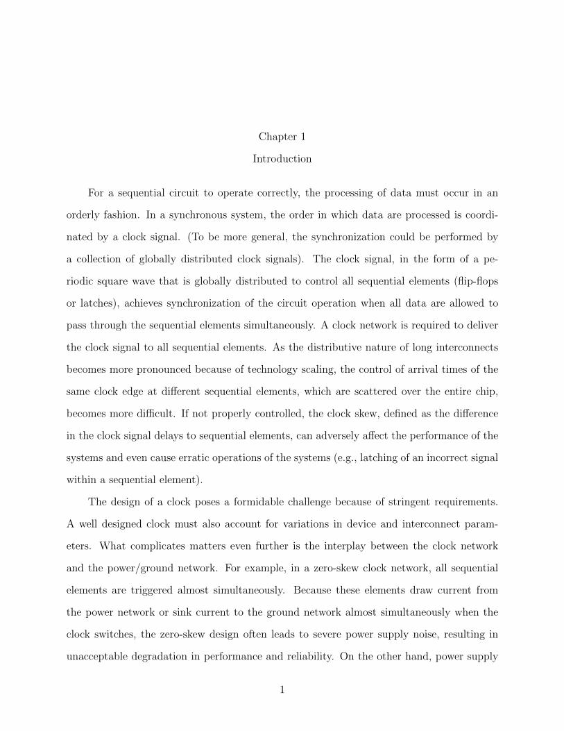
For a sequential circuit to operate correctly, the processing of data must occur in an
orderly fashion. In a synchronous system, the order in which data are processed is coordi-
nated by a clock signal. (To be more general, the synchronization could be performed by
a collection of globally distributed clock signals). The clock signal, in the form of a pe-
riodic square wave that is globally distributed to control all sequential elements (flip-flops
or latches), achieves synchronization of the circuit operation when all data are allowed to
pass through the sequential elements simultaneously. A clock network is required to deliver
the clock signal to all sequential elements. As the distributive nature of long interconnects
becomes more pronounced because of technology scaling, the control of arrival times of the
same clock edge at different sequential elements, which are scattered over the entire chip,
becomes more difficult. If not properly controlled, the clock skew, defined as the difference
in the clock signal delays to sequential elements, can adversely affect the performance of the
systems and even cause erratic operations of the systems (e.g., latching of an incorrect signal
within a sequential element).
The design of a clock poses a formidable challenge because of stringent requirements.
A well designed clock must also account for variations in device and interconnect param-
eters. What complicates matters even further is the interplay between the clock network
and the power/ground network. For example, in a zero-skew clock network, all sequential
elements are triggered almost simultaneously. Because these elements draw current from
the power network or sink current to the ground network almost simultaneously when the
clock switches, the zero-skew design often leads to severe power supply noise, resulting in
unacceptable degradation in performance and reliability. On the other hand, power supply
1
noise affects the clock jitter (this refers to the time shift in the clock pulse, as well as the
variations in the pulse width that arise from the time-varying operating conditions such as
supply voltage), which, in turn, affects the arrival times of clock signal at different sequential
elements.
Currently, a digital (and electrical) clock signal is distributed using metallic intercon-
nects (e.g. Cu) throughout the entire die. There are many approaches to distribute digital
clock signals, such as H-trees, grids and some combinations of them [42, 46]. In this project,
we will consider buffered H-trees driving local grids as representative of present clock dis-
tribution, to which we will refer as the conventional approach. Advanced active de-skewing
techniques, which further improve the quality of standard clock distribution, are not consid-
ered in this simple analysis [46].
Several interconnect solutions have been proposed to mitigate the increasingly difficult
clock distribution, 3-D, optical, and RF being the most important ones. 3-D interconnects,
which refers to two or more active Si strata that are integrated together (for example by
bonding), take advantage of the vertical dimension to decrease the die size, therefore allevi-
ating clock distribution (see, for example, [5, 12, 41, 28]). Optical interconnects have also
been proposed for clock distribution since they are immune to crosstalk noise from adjacent
electrical interconnects, and because of their speed-of-light propagation. Optical intercon-
nects also have the potential for large bandwidths, which are mostly relevant for signalling
[32, 44]. RF approaches using Cu interconnects have been proposed as a low-power clock dis-
tribution alternative at the package level [43]. The main difference between the RF approach
and conventional approach is that RF uses a narrow-band sinusoidal wave for transmitting
the clock signal as opposed to the digital square signal that is employed in conventional
clock distribution. An interesting wireless RF clock distribution, in which the clock signal is
broadcast by a source and received by on-die antennae, has also been proposed and investi-
gated in [16]. This technique is attractive since it does not require interconnects. However,
noise considerations as well as the size and position of the antennae are technical and cost
2

issues that have to be addressed. Most of the benchmarking research has been confined to
global clock distribution. However, in order to truly assess the overall benefits of alternative
clock distribution approaches, it is also important to include the local clock distribution in
the analysis.
1.1 Definitions
1.1.1 Clock Skew
A synchronous digital system typically consists of a series of registers, between which
are blocks of combinational logic. The functional requirements of the system are met by
these blocks of combinational logic, while the registers provide the global performance and
satisfy the local timing requirements. The registers are typically inserted in such a way that
the combinational logic is partitioned into several time windows of ideally equal duration.
This partitioning, known as pipelining, enables the system to run at higher frequencies than
if the entire logic path was implemented uninterruptedly.
The operation of a single stage in a pipelined synchronous system can be broken down
as follows. Each data signal is stored in a register. The arrival of the clock signal latches a
new value of the data into the register. At this time the data propagates through the register
and into the combinational block of logic. The signal passes through this network of logic,
arrives at the input of the next register, and, for a properly functioning system, is stored on
the next latching clock edge. Thus, the components of delay through a local data path are
the delays associated with the register, the delay through the logic and interconnect between
registers, and the delays involved with the clock signal distribution.
One of the primary concerns in the design of a clock distribution network is the differ-
ence in the arrival times of the clock edge between two registers. This difference is called
clock skew, and the goal is to minimize, manage, or eliminate this term altogether. Clock
skew is most important between sequentially adjacent registers. A sequentially adjacent
3

pair of registers is defined as two registers between which lie only combinational logic and
interconnect. A formal definition for clock skew given by Friedman in [18] is repeated below.
Given two sequentially-adjacent registers, RI and RJ, and an equipotential clock distri-
bution network, the clock skew between these two registers is defined as TSKEW(I,J) = TCI -
TCJ, where TCI and TCJ are the clock delays from the clock source to the registers RI and
RJ, respectively.
Though the definition specifically states that clock skew is a characteristic of sequentially
adjacent registers, it exists, in fact, between any two registers, but is only truly significant
between registers that share direct communication. The presence of clock skew can severely
limit the performance of a synchronous system, and even create a race condition that causes
incorrect data to be latched in a register.
In order to minimize clock skew, it is first necessary to understand the sources of clock
skew. Wann and Franklin reported the following sources of clock skew [51]:
• differences in line lengths from the clock source to the clocked register;
• differences in delays of any active buffers within the clock distribution network;
• differences in passive interconnect parameters, such as line resistivity, dielectric con-
stant and thickness, via/contact resistance, line and fringing capacitance, and line
dimensions; and
• differences in active device parameters, such as MOS threshold voltages and channel
mobilities, which affect the delay of the active buffers.
Layout techniques and careful clock distribution design can minimize the effects of items
one and three above. In well designed systems, the distributed active clock buffers contribute
most significantly to the overall clock skew.
The delay components of a local data path, briefly mentioned earlier, can be formalized
with the following equation. This relation details the components of the path delay, from an
initial register RI to a final register RF and is illustrated in Figure 1.1.
4

Figure 1.1: Delay components of a local data path.
TPD = TC-Q + T LOGIC + T INT + T SETUP (1)
This relation states that the total delay of a path is equal to the sum of the clock to
output delay of the register, TC-Q, the total delay of the logic path between registers, TLOGIC,
the total delay of the interconnect, TINT, and the necessary setup time that must be met
at the final register for correct operation, TSETUP. This total path delay is related to the
maximum clock frequency possible between two registers by the relation:
1/fMAX = TCP(MIN) ≥ TPD + T SKEW (2)
where fMAX is the maximum clock frequency, TCP(MIN) is the minimum cycle time, and TSKEW
is the clock skew between the two registers. Though it has not yet been mentioned, it should
be noted that clock skew can be a negative or positive value depending on whether the clock
signal at the final register lags or leads that at the initial register. This discussion leads
naturally into the effects of clock skew on system performance.
Depending on the magnitude and polarity of the clock skew, system performance can
be either enhanced or degraded. The presence of skew defines a set of equations describing
the constraints that clock skew imposes on the system timing.
Ignoring the clock skew term in equation (2), it is apparent that the maximum attainable
frequency in a system is that given by the inverse of the longest path delay between any
two sequentially adjacent registers RF and RI [50]. If the arrival of the clock signal at RF
5

leads that of RI then positive clock skew exists. Positive clock skew serves to increase the
path delay as shown in equation (2). This increase in path delay decreases the maximum
clock frequency, decreasing performance. Thus, positive clock skew is the amount of time
that must be added to the minimum clock period to reliably transfer data through a system.
The tolerance of a system to positive clock skew can be described by combining equations
(1) and (2).
T SKEW ≤ TCP − TPD(MAX) = TCP − (TC-Q + T LOGIC(MAX) + T INT + T SETUP) (3)
At any particular clock frequency, this equation must be satisfied for the system to
function correctly. For paths that have low tolerance to skew (TCP - TPD is small), the
clock signal should be routed such that the initial register receives the signal before the final
register, imposing negative clock skew on the particular path.
As opposed to positive clock skew, negative clock skew can improve performance of
a synchronous system. Between two sequentially adjacent registers, RI and RF , negative
clock skew implies that the clock signal at RF lags that of RI. Considering equation (2) it is
apparent that negative clock skew decreases the amount of time needed between two registers
given a particular path delay, TPD. However, the existence of negative clock skew in a path
imposes a constraint on the minimum path delay. If the amount of skew is greater than the
time required for a signal to propagate from RI through the interconnect and logic to RF,
then the data from the current clock period has overwritten that from the previous period
before it was latched into RF. This creates a race condition which is a catastrophic error in
a synchronous system. What is even worse is that this is a delay-dependent condition that
may only surface under certain operating conditions (ambient temperature, system activity,
etc.). For operation to continue correctly, the final register RF must latch the previous data
from RI before the new data is allowed to propagate through to RF. This constraint is given
by the following equation:
|T SKEW| ≤ TPD(MIN) = TC-Q + T LOGIC(MIN) + T INT − THOLD (4)
6

Figure 1.2: Illustrations of positive and negative clock skews.
In equation (4), TPD(MIN) is the minimum path delay between sequentially adjacent registers,
and THOLD is the time that the input signal must be stable at the final register after the
clock signal has arrived.
An obvious use for negative clock skew is the reduction of critical path delays, thus
increasing system performance. If a designer forces the arrival of the clock at RI to lead
that of RF, the data from RI has a longer time to propagate to RF. This shifts time from
the previous local path (the path where RI is the final register), to the presumably more
critical path. This technique allows the designer to optimize the clock distribution to the
path delays, allowing a means to compensate for uneven partitioning of the local data paths
within a global data path.
1.1.2 Power Dissipation
The focus of most contemporary clock distribution network designs is the power dissi-
pation associated with the clock signal. Increasing die sizes and operating frequencies have
resulted in a significant, and sometimes inordinate, percentage of a chip power dedicated
7

to the clock distribution. This cause and effect can be simply represented by the dynamic
power equation:
P = CV2f
where C is the capacitive load, f is the switching frequency and V is the voltage swing of the
signal.
The DEC Alpha 21164 microprocessor illustrates the extent to which the clock distribu-
tion network power dissipation can become a problem. The 21164 is a 16.5 mm × 18.1 mm
chip with 3.75 nF of capacitance on the clock net. With an operating frequency of 300 MHz
and a power supply of 3.3 V, the clock distribution dissipates 65% of the 50 W consumed
by the chip [8, 33].
In microprocessor designs of today the total power dissipation is a major concern. The
present trends quickly result in power dissipations that complicate system-level design. For
this reason a lot of attention is being focused on reducing the processor’s total power dissi-
pation, including that of the clock distribution.
Examination of the above equation should reveal one of the best ways for reducing a
chip’s total power dissipation. Decreasing the power supply voltage reduces the squared
term in the power equation. Since this affects all logic gates, including those associated with
the clock distribution, it has a significant effect on the power dissipation. Recent trends
have seen the power supply voltage decrease from 5.0 V, to 3.3 V, to 2.8 V, to 2.0 V for
the core logic of DEC Alpha 21264. Obviously, this trend represents a significant decrease
in the dynamic power dissipation, but there are limits on how low power supply voltages
can go. Noise tolerance issues will keep the power supply voltage from falling much lower,
while increasing die area and operating frequency will continue to contribute to the chip’s
dynamic power dissipation.
The sharp transitions required on the clock net are another cause for increased power
dissipation. As the RC product of the clock network increases, the rise and fall times of
the clock signal will increase unless there exists a corresponding increase in power. Typical
8

efforts to reduce the RC product include routing the clock net in low-resistivity metal layers,
minimizing the capacitive load presented by the register elements, and detailed design of the
clock network to trim off excess length and width (thus minimizing capacitance). Another
common method is to use multiple levels of clock buffering. This has the effect of separating
the high resistive load of the long clock nets from the high capacitive load of the register
elements. More detail on clock distribution methods will be covered in a following chapter.
A third method of reducing the power dissipation in the clock network is to shut off
the clock signal to unused portions of the chip. This method is used to significant gain on
the DEC StrongARM microprocessor. It is estimated that conditional clocking reduced the
power dissipation of the StrongARM’s clock network almost four-fold [33].
1.1.3 Jitter
Increasing clock frequencies reveal a problem that has been previously considered neg-
ligible. A general design rule of thumb is that 10% of the clock period is allocated to clock
skew. With designs such as the DEC Alpha 21164 reporting a peak skew of 80 ps [8] at a
clock period of 3.33 ns this rule seems easy to meet. However, future generation processors
will see clock periods on the order of 1 ns. While clock skew itself may still be manageable
at these frequencies (assuming die sizes remain the same), the quantity called jitter has yet
to be considered.
Jitter represents the time varying behavior of the clock signal. Noise from various
sources cause perturbations on the clock network that can cause any receiver of the clock
signal to perceive a transition at a different time. Since the noise events are typically random
in nature, their effect on system timing is also random.
From the clock generator itself, down to the register elements, jitter affects system timing
in an unpredictable fashion. The jitter performance of a typical phase-locked loop clock
generator is 150 ps. This implies nothing about the jitter introduced along the network in
9

the buffers or registers. Obviously, this quantity will become significant for future generation
systems. The noise sources that contribute to jitter most significantly are the following:
• Noise coupled through the circuit’s power and ground connections;
• Noise coupled through adjacent or intersecting traces;
• Noise inherent to the circuit’s transistors themselves.
10

Chapter 2
The Clock Distribution Network
This section will discuss some design issues and methodologies for each of three general
stages in a clock distribution network:
• the clock generator;
• the global clock distribution;
• the local clock distribution.
Where appropriate, the sections will cover design issues relating to the topics of clock
skew, power dissipation, and jitter.
2.1 Clock Generation
There are many issues to consider in the design of a clock generator. Both power
dissipation and jitter play a major role in determining the type of generation system to
utilize. Obviously, operating frequency also plays a major role, especially in the present
day systems. The large discrepancy between system clock frequency and processor clock
frequency inevitably results in the need for a phase locked loop (PLL) clock generator.
Figure 2.1 illustrates the basic block diagram of a phase locked loop (PLL)-based clock
generator. The benefits of such a clock generator are two-fold. First, the frequency of the
clock generator output can be a multiple of the main system clock frequency. This allows
the integrated circuit to run at a higher frequency than the rest of the system, while main-
taining synchronization. This is important for microprocessors, because the advancement of
the system bus frequency has traditionally lagged the advancement of the microprocessor
11

Figure 2.1: A generic phase locked loop (PLL) block diagram.
frequency. Use of an on-chip PLL has allowed microprocessors to continually increase in
performance while only marginal gains in system bus performance were made. Second, in
a synchronous system, use of a PLL clock generator can eliminate clock skew from active
device variation between chips or even on the same chip. Since the output of the PLL is
in-phase with the input, if the clock distribution buffers are included within the loop (as
illustrated in Figure 2.1), their delay is essentially removed from the system. This does
not eliminate the chip-to-chip or on-chip clock skew due to passive device variations and
interconnect delay [4].
These important advantages to PLL clock generation do not come without a price. A
PLL, unless designed completely from digital circuitry, is essentially an analog circuit, and
requires very careful design. The noise inherent in a digital system, especially a high-speed
microprocessor, can cause many problems for a PLL clock generator. Furthermore, PLLs
typically require relatively large passive elements for stable operation. Some integrated
circuit technologies do not lend themselves well to the creation of such structures. Last,
but certainly not least, even a well-designed PLL exhibits variation in its output phase and
frequency over time. This quantity is the jitter term introduced in Section 1.1.3.
The components of a PLL that are most susceptible to noise are the phase detector,
charge pump, and voltage-controlled oscillator (VCO). With careful layout and circuit design
the jitter due to noise in the phase detector and charge pump can be largely eliminated, but
the VCO is a very sensitive circuit that bears closer inspection.
12

2.1.1 Global Clock Distribution
The global clock distribution concerns the means by which the clock signal is relayed
from the clock generator to the register loads. The routing, buffering, and signaling method-
ologies are major design decisions and have significant impact on overall system perfor-
mance. The timing requirements involved in the clock distribution network make its design
a very difficult one. In fact, system level trade-offs between system speed, physical die
area, and power dissipation are significantly affected by the design of the clock distribution
network [18]. This section discusses some traditional methods for global clock distribution
design and their characteristics in terms of clock skew, power and jitter.
2.1.2 Clock Tree
By far the most common method for distributing clock signals in VLSI applications is
the clock tree method. This tree structure is so called because buffers are placed between
the clock source and along the clock paths as they branch out towards the clock loads.
Figure 2.2 illustrates the organization of a clock tree distribution network. The distributed
buffers amplify the clock signal to remove any degradation of the signal due to interconnect
resistance between the clock source and the registers. In this scheme, it should be noted,
the distributed buffers are the primary source of the total clock skew because active device
characteristics typically vary more than passive device characteristics.
An extension of this scheme is demonstrated by the DEC Alpha 21064 microprocessor
(Figure 2.3). In this five stage buffer tree design, one of the intermediate clock tree stages
was made into a mesh by strapping metal lines across each of the branches. The mesh
structure places the interconnect resistance in parallel, reducing the effective resistance seen
by the buffers. This minimizes both the delay through the clock distribution and the total
skew within it [15]. Furthermore, the inputs to previous buffer stages were strapped together
to smooth any asymmetric arrival times of the clock signal.
13

Figure 2.2: Buffer-tree clock distribution.
If the interconnect resistance from the clock source to the registers is negligible, then
the clock tree scheme can be reduced to a single buffer driving the entire network. The
advantages of this strategy are the removal of the skew introduced by the distributed buffers,
and the reduced area obtained by eliminating the distributed buffers. However, the single
buffer must be capable of providing enough current to drive the network capacitance of the
interconnect and register loads, while maintaining sharp, consistent transitions. A recent,
and somewhat notorious, example of this clock distribution strategy is the DEC Alpha 21164
microprocessor. In this clock distribution network, a tree of buffers converges on a single
buffer which drives the entire clock load of 3.75 nF. This final inverter consists of 58 cm of
transistor and is required to drive the clock signal at 300 MHz [8]. This design resulted in an
incredibly low maximum clock skew of 80 ps across the 16.5 mm x 18.1 mm die. However,
the price for this performance was the dissipation of nearly 65% of the total processor power
of 50W in the clock distribution network [8, 33].
14
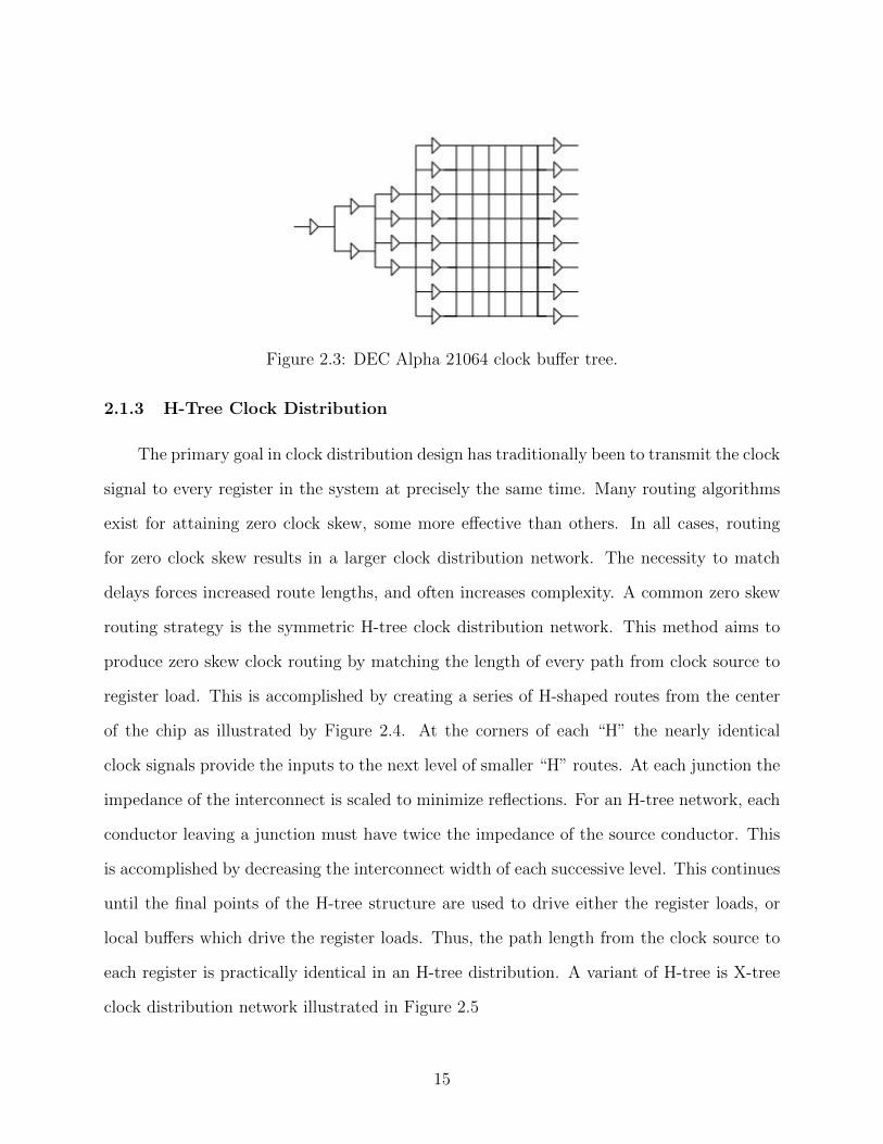
Figure 2.3: DEC Alpha 21064 clock buffer tree.
2.1.3 H-Tree Clock Distribution
The primary goal in clock distribution design has traditionally been to transmit the clock
signal to every register in the system at precisely the same time. Many routing algorithms
exist for attaining zero clock skew, some more effective than others. In all cases, routing
for zero clock skew results in a larger clock distribution network. The necessity to match
delays forces increased route lengths, and often increases complexity. A common zero skew
routing strategy is the symmetric H-tree clock distribution network. This method aims to
produce zero skew clock routing by matching the length of every path from clock source to
register load. This is accomplished by creating a series of H-shaped routes from the center
of the chip as illustrated by Figure 2.4. At the corners of each “H” the nearly identical
clock signals provide the inputs to the next level of smaller “H” routes. At each junction the
impedance of the interconnect is scaled to minimize reflections. For an H-tree network, each
conductor leaving a junction must have twice the impedance of the source conductor. This
is accomplished by decreasing the interconnect width of each successive level. This continues
until the final points of the H-tree structure are used to drive either the register loads, or
local buffers which drive the register loads. Thus, the path length from the clock source to
each register is practically identical in an H-tree distribution. A variant of H-tree is X-tree
clock distribution network illustrated in Figure 2.5
15
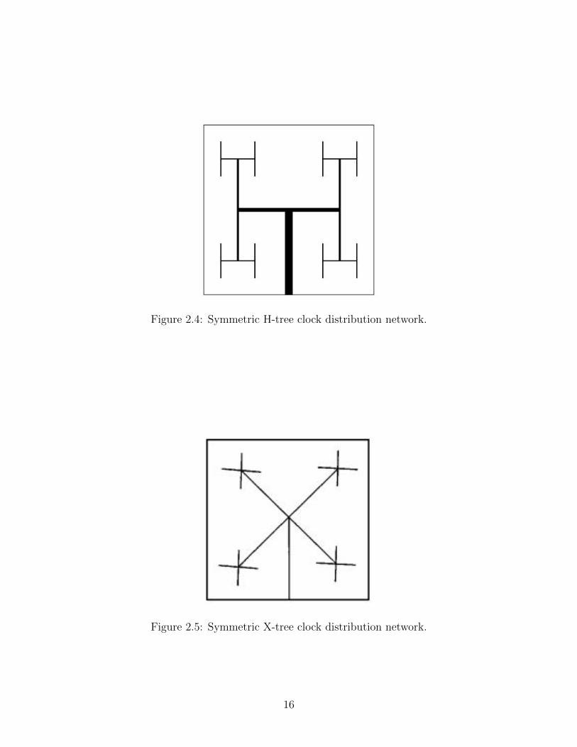
Figure 2.4: Symmetric H-tree clock distribution network.
Figure 2.5: Symmetric X-tree clock distribution network.
16

Obviously, this method does not truly produce zero clock skew. At some point the clock
signal must be routed to the registers. Within this local block, clock skew will exist, but the
block size is chosen such that the skew is insignificant. Other sources of skew include the
variation in interconnect parameters, and the variation in active parameters for any buffers
distributed through the H-tree network.
Since the magnitude of the clock skew is only significant for sequentially adjacent reg-
isters, the symmetry provided by an H-tree distribution is largely unnecessary. Considering
the additional interconnect capacitance (which leads to increased power dissipation), the
benefits of zero clock skew may not be worthy of the price. In fact, the use of an H-tree
structure is often overkill for even current generation microprocessors [23].
Even if sequentially adjacent registers are located on opposite sides of a chip, the concept
of tolerable skew routing seems more effective. Allowing a measure of clock skew between
registers significantly relaxes wiring constraints. This relaxation reduces overall interconnect
capacitance and power dissipation. A method for routing a two level clock network with
tolerable clock skew is reported in [54]. Though this project details only a planar, equal
path length routing algorithm for the first level of the clock network, it demonstrates that a
tolerable skew methodology can yield a lower total interconnect length. A method that not
only uses tolerable clock skew, but takes advantage of optimal skew scheduling is reported
in [36]. Part of a four step design process, this method inserts buffers with tuned delays to
achieve an optimal clock skew schedule. This not only reduces the overall clock interconnect
length, but increases system performance by allowing a higher frequency.
Routing and distributing the clock signal are only part of the design process. The
method of clock signaling must also be determined. Typically, the clock signal is not treated
any differently than any other signal in this respect. However, the use of alternative clock
signaling methods achieve significant power savings, often at minimal cost to performance
and area.
17

Figure 2.6: Half-swing clock signaling methodology.
Figure 2.6 illustrates the difference between a conventional, full-swing clock signaling
methodology, and a half-swing methodology proposed by Kojima et al. [26]. Recalling that
dynamic power dissipation is proportional to V2, it is readily apparent that routing two
half-swing pairs of clock signals results in approximately 50% the power dissipation of one
pair of full-swing clock signals.
Very often additional clock signals are required by reduced-swing methodologies because
the differential signaling is necessary to offset the reduced noise tolerances. This obviously
has the effect of complicating the clock routing since additional signals must be routed.
Unfortunately, this has the secondary effect of increasing clock load, since the differential
clock nets must be routed close to one another. This prevents the power savings from
achieving the theoretical 50% reduction.
If the clock distribution were designed around noise-tolerant circuits, it might be possible
to utilize a reduced-swing methodology without the additional clock signals. This would
harness all the benefits of voltage swing reduction.
Power reduction is also possible through conditional clocking. By using a conditional
buffer to drive the register elements (which comprise the majority of capacitive clock load)
the system is able to disable the clock signal in idle sections. This effectively reduces the
capacitive loading seen by the clock distribution and directly reduces the power dissipation
18
of the network. The StrongARM RISC microprocessor from DEC used this technique to
help achieve a very impressive power-performance point. The 2.5 million transistor device
operates at a frequency of 160 MHz, while only dissipating 450 mW of power. Of the five
clocking regimes on the chip, four are sourced by conditional clock buffers. The use of gated
clocks does not come without a price. The logic paths associated with enabling/disabling
the particular clock buffers were some of the most difficult to design. However, the DEC
design team made the decision that the power savings justified the increase in complexity
and potential degradation of performance. In fact, it is estimated that the 15% of the chip
power that is dissipated in the clock network could have quadrupled without the use of gated
clocks [33].
Recent research has reported other applications for gated clocks. In 1995, Benini and
De Mecheli [6] reported a method of designing finite state machines that takes advantage of
self-loops within the FSM to gate the clock. For a set of benchmark circuits they achieved
an average power savings of 25% with an area cost of only 5%. Digital signal processors
also benefit from the use of conditional clocking. The multi-hundred MHz multipliers used
in FIR filters dissipate a large fraction of their power in the clock network. Nagendra and
Irwin [35] propose a method for reducing the activity factor of a multiplier, thus decreasing
the power dissipation.
19
Chapter 3
Wireless Clock Distribution
Clock distribution is a crucial aspect of modern multi-GHz microprocessor design. Con-
ventional distribution schemes are more or less monolithic in that a single clock source is fed
through hierarchies of clock buffers to eventually drive almost the entire chip. This raises
a number of challenges. First, due to irregular logic, the load of the clock network is non-
uniform, and the increasing process and device variations in deep sub-micron semiconductor
technologies further adds to the spatial timing uncertainties known as clock skews. Second,
the load of the entire chip is substantial, and sending a high quality clock signal to every
corner of the chip necessarily requires driving the clock distribution network “hard”, usually
in full swing of the power supply voltage. Not only does this mean high power expenditure,
but it also requires a chain of clock buffers to deliver the ultimate driving capability. These
active element are subject to power supply noise, and add delay uncertainty jitter which
also eats into usable clock cycle. Jitter and skew combined represent about 18% of cycle
time currently [21], and that results in indirect energy waste as well. For a fixed cycle time
budget, any increase in jitter and skew reduces the time left for the logic. To compensate
and make the circuitry faster, the supply voltage is raised, therefore increasing energy con-
sumption. Conversely, any improvement in jitter and skew generates timing slack that can
be used to allow the logic circuit to operate more energy efficiently.
As commercial microprocessors are rapidly becoming multi-core systems, monolithic
clock distribution will be even less applicable. In the era of billion-transistor microprocessors,
a single chip is really a complex system with communicating components and should be
treated as such. In communication systems, synchronizing clocks is also a rudimentary and
20

crucial task. In this section, we will discuss the concept of wireless clock distribution network
in a microprocessor.
Wireless interconnect should provide an additional means for global communications,
freeing up conventional wires for other uses. This new interconnect technology is being
developed utilizing a clock distribution system as the driver. Using wireless interconnects
in a clock distribution system should reduce the latency in the clock tree which should
help reduce clock skew [1] and should eliminate the frequency dispersion problem that may
ultimately limit the maximum clock frequency [14].
A conceptual illustration of a single-chip or intra-chip wireless interconnect system for
clock distribution is shown in Figure 3.1. An approximately 20-GHz signal is generated
on-chip and applied to an integrated transmitting antenna which is located at one part of
the IC. Clock receivers distributed throughout the IC detect the transmitted 20-GHz signal
using integrated antennas, and then amplify and synchronously divide it down to a ∼2.5-
GHz local clock frequency. These local clock signals are then buffered and distributed to
adjacent circuitry. Figure 3.2 shows an illustration of a multi-chip or inter-chip wireless clock
distribution system. Here the transmitter is located off-chip, utilizing an external antenna,
potentially with a reflector. Integrated circuits located on either a board or a multi-chip
module each have integrated receivers which detect the transmitted global clock signal and
generate synchronized local clock signals.
3.1 Clock Transmitter
Figure 3.3 shows a simplified block diagram for an integrated clock transmitter. The
20-GHz signal is generated using a voltage-controlled oscillator (VCO). The signal from the
VCO is then amplified using a power amplifier (PA), and fed to the transmitting antenna.
The VCO is phase-locked to an external reference using a phase-locked loop (PLL), providing
frequency stability. The PLL consists of a phase-frequency detector (PFD), a loop filter, the
VCO, and a frequency divider.
21

Figure 3.1: Intra-chip wireless interconnect system.
Figure 3.2: Inter-chip wireless interconnect system.
Figure 3.3: Block diagram of integrated clock transmitter.
22

Figure 3.4: Block diagram of integrated clock receiver.
3.2 Clock Receiver
Figure 3.4 shows a block diagram for an integrated clock receiver. The global clock
signal is detected with a receiving antenna, amplified using a low noise amplifier (LNA), and
divided down to the local clock frequency. These local clock signals are then buffered and
distributed to adjacent circuits. The amplifier is tuned to the clock transmission frequency to
reduce interference and noise. Since the microprocessor is extremely noisy at the local clock
frequency and its harmonics, transmitting the global clock at a frequency higher than the
local clock frequency provides a level of noise immunity for the system [30]. Also, operating
at a higher frequency decreases the required antenna size. The receiver is implemented in a
fully differential architecture, which rejects common-mode noise (e.g., substrate noise) [9, 30],
obviates the need for a balanced-to-unbalanced conversion between the antenna and the LNA,
and provides dual-phase clock signals to the frequency divider.
3.3 Comparison of Power Consumption with Conventional Methods
Kenneth et al. [17] have discussed the power consumption in a wireless clock distribution
network and given a comparison with conventional clock distribution network’s. To compare
the power requirements between different types of global clock distribution systems, the
system voltage and frequencies are assumed to be equal. Also, an equal capacitive load
representing the local clock generators or distribution system is assumed for each type of
global distribution system. Under these assumptions, the power dissipation can be converted
23

to capacitances and these can be used to compare the power dissipation of different global
distribution systems, similar to an approach taken in [42].
The total global capacitance can be allocated among three components: CG, CW, and
CL. CG is the equivalent capacitance of the highest level network which delivers the clock
from its source to spine locations distributed throughout the chip. CG includes the total
capacitance of the final driver stage, herein termed the sector buffer, plus any buffers leading
up to the sector buffer. The sector buffers are assumed to be exponentially tapered for
minimum delay [29]. CW is the capacitance of the interconnecting wires for delivering the
clock from the spine locations to the local distribution system. CL is the load capacitance
representing the input capacitance of the local clock generators.
Two cases are used in comparing these clock distribution systems for 0.1-um generation
microprocessors. Case 1 is for aluminum interconnects and conventional dielectrics; case 2
is for copper interconnects and low-K dielectrics.
3.3.1 Grid Based System
The grid-based system, based on DEC 21264 [19], consists of a global tree supplying the
clock to different spine/buffer locations, and the capacitance of this network is CG. These
buffers drive the clock grid, which has capacitance CW. The local clock generators tap off
of the grid. Due to the amount of wiring used to form the grid, CW is large. Consequently,
large sector buffers are needed, increasing CG.
3.3.2 H-Tree Based Systems
The H-tree system, based on IBM S/390 [52], consists of a global tree supplying the
clock to different spine/buffer locations. Each buffer drives a balanced H-tree, which drives
the local clock generators. CW is smaller for the H-tree, therefore a smaller sector buffer is
required.
24

Table 3.1: Global capacitive loading.
3.3.3 Wireless System
The wireless system consists of a clock transmitter broadcasting a microwave signal to
a grid of distributed receivers. A receiver corresponds to a spine location. Due to their low
capacitance, balanced H-trees are used to distribute the signal from the receivers to the local
clock generators. Thus, CW for both the H-tree and wireless schemes are equal. In wireless
clock distribution systems, long interconnects for delivering the clock from its source to
spine locations are not present and the associated component of CG is zero. However, since
the wireless system contains components with static power dissipation, an equivalent global
capacitance, representing this power dissipation, is needed. This capacitance is then used to
make a comparison to the grid and H-tree systems. To obtain this equivalent capacitance, the
total power dissipation of the clock transmitter and receivers is divided by the factor (V2f).
Table 3.1 shows a breakdown of the global capacitive loading for the three distribution
systems for cases 1 and 2, and includes the initial 0.25-um data. All capacitance units are
in pF. The final row gives the power consumed by the global clock distribution systems as a
percentage of total microprocessor power. This percentage represents the relative amount of
power dissipated in the global system to drive a load of CL. The results show that for both
cases, the wireless system is comparable in performance to the H-tree system and better in
performance than the grid-based system in terms of power dissipation. The results also show
25
that technology developments such as Cu or low-k will have the greatest positive impact on
systems whose total equivalent capacitance is dominated by CW, such as the grid. Finally,
the results show that the power dissipated in the clock receivers, given by CG, should be a
small fraction (2.3%) of the total power dissipated in the microprocessor. These results show
that power dissipation does not impose limitations for wireless clock distribution systems.
However, additional work focused on the overall feasibility and implementation of this system
is ongoing.
3.4 Potential Benefits
The wireless clock distribution system would address the interconnect needs of the
semiconductor industry in providing high-frequency clock signals with short propagation
delays. These needs would be met while providing multiple benefits. First, signal propagation
occurs at the speed of light, shortening the global interconnect delay without requiring
integrated optical components. Second, the global interconnect wires used in conventional
clock distribution systems are eliminated, freeing up these metal layers for other applications.
Third, referring to Figure 3.2, the inter-chip clock distribution system can provide global
clock signals with a small skew to an area much greater than the projected IC size. This is
an additional benefit, possibly allowing synchronization of an entire PC board or a multi-
chip module (MCM). Fourth, in the wireless system, dispersive effects are minimized since
a monotone global clock signal is transmitted. Fifth, another benefit is a more uniformly
distributed power load equalizing temperature gradients across the chip. Sixth, by adjusting
the division ratio in the receiver, higher frequency local clock signals [1] can be obtained, while
maintaining synchronization with a lower frequency system clock. Seventh, an intangible
benefit of wireless interconnect systems is the effect they could have on microprocessor or
system implementations, potentially allowing paradigm shifts such as drastically increased
chip size. Finally, compared to other potential breakthrough interconnect techniques, such
as optical, superconducting, or organic, a wireless approach based on silicon seems to be
26

a potential solution which is compatible with the technology trends of the semiconductor
industry.
3.5 Areas of Research
The main areas of research for wireless clock distribution are as follows: integrating com-
pact power-efficient antenna structures, identifying noise-coupling mechanisms for the wire-
less clock distribution system and estimating the signal-to-noise ratio that can be achieved
on a working microprocessor, implementing the required 20-GHz circuits in a CMOS process
consistent with the ITRS [1], and characterizing a wireless clock distribution system in terms
of skew and power consumption and estimating the overall feasibility of the system.
27

Chapter 4
Optical Clock Distribution
Designing clock distribution networks is a big challenge for future microprocessors due
to increasing frequency, power, transistor counts and process variations. As technology
scales, implementing conventional clock distribution networks that meet low power and skew
requirements is becoming more difficult. On the other hand, optical interconnects are being
proposed as an alternative to electrical interconnects due to their speed-of-light transmission,
high bandwidth and low power dissipation. In the future, interconnects between chips,
between cores on a chip and within components on a processor core could be made optical
to achieve lower power and higher performance.
Optical interconnects for clock distribution were first studied by Goodman et al. [20].
They postulate that interconnect delays will be the limiting factor for performance in future
MOS circuits and suggest moving to optical and electro-optic technologies. With near-
infrared optical sources, modulators and detectors with media such as free space, optical
fibers and integrated optical waveguides, they state the interconnect scaling problem could
be solved.
They list five advantages in moving to photonics: freedom from capacitive loading
effects which allows greater fan-in and fan-out, immunity to mutual interference effects,
lack of planar constraints resulting in reduced cross-coupling for criss-crossing waveguides,
reconfigurability of free space focused interconnects and possibility of direct injection of
optical signals into electronic devices without the need for optical to electrical conversion.
Four ways of optical clocking are described next:
28

• Index-based with waveguides - light is carried from a single source generating the optical
clock signal to the other parts of the chip using waveguides which are integrated on a
suitable substrate.
• Index-based with fiber optics - light is transmitted similar to the above case except
that fibers are used instead of waveguides in a separate core.
• Unfocused free space interconnect - optical clock signal broadcast to the entire chip by
focusing light (through a lens or diffusers) perpendicular to the chip from above.
• Focused free space interconnect - an optical element like a hologram (which acts as a
grating) sends the optical signals onto a multitude of detection sites simultaneously.
Miller et al [31, 32] discuss various opportunities for optics in on-chip interconnects
and notes that one of the main reasons to move away from long electrical on-chip wires
is to avoid growing transmission line and inductance effects. Power requirements of long
point-to-point optical interconnects are much lower (with no need for repeaters for optical
clock transmission), and optical signals, whether long or short, perform equally well. Other
benefits include the ability to send signals across in the 3rd dimension and the possibility
of integration with electronic devices. Debaes et al. [13] and Bhatnagar [7] discuss the
advantages of optical clocking and propose a receiver-less optical clocking scheme which
reduces the latency of transmitting the clock signal to the local network. They conclude
that such a latency-reducing scheme reduces skew and jitter but does not reduce the power
consumed compared to an electrical clocking scheme.
Recent studies comparing electrical and optical clocking schemes have analysed the
power, skew and area usage for different technologies and estimated the potential of photonics
in clock distribution [11, 25]. Based on the 2001 ITRS roadmap [2], using analytical models,
they estimate that most of the power dissipation is associated with local clock distribution.
Since alternatives to electrical clock distribution have been proposed for replacing the global
clock distribution only, they conclude that there are no significant power benefits to replacing
29

electrical distribution with optical distribution. The paper also shows that low skew can be
obtained with optical as well as non-scaled electrical interconnects (130nm) and concludes
that skew benefits of optical transmission are also not significant if non-scaled electrical
interconnects are used. They consider a global balanced and buffered H-Tree driving local
grids as representative of current clock distribution techniques. For optical distribution, they
replace the electrical H-tree by an H-tree structure built using waveguides with detectors at
the end points to convert the light pulses to a clock signal. The local grids and buffers
driving the local grids remain the same in both implementations.
Mule et al. [34] discuss the pros and cons of electrical and optical clock distribution
systems. Among the different schemes used to transmit the optical clock onto different
parts of the chip, they find the waveguide based approach most feasible since free-space
approaches work in 3 dimensions (and hence are not compact) and this would complicate
power distribution and cooling. To accomplish local clock routing with optical technology,
the fanout should correspond to the total number of latches on the chip. Since optical
signals do not use repeaters and rely on the original source strength to drive all the loads,
it is extremely difficult to make the fanout more than a few tens or hundreds of loads at
the most. Hence for the regions which require short wires like the local distribution regions,
current systems can only use electrical routing.
A possible implementation of optical clocking is to replace the global transmission net-
work with optical waveguides and use electrical local distribution. At the end of the global
transmission network, when the global clock signal is converted to electrical signals using a
detector, it has to be buffered and amplified and sent to the local network. However, given
expected optical technologies, the number of fanouts on the global optical transmission must
be relatively small (less than 100). This means that the electrical fanout driven by each op-
tical receiver will be quite large (thousands of latches). In order to make the optical receiver
fast and to support large optical fanouts, each optical receiver must be physically small and
have a very small capacitance. However, taking a signal on a very small capacitance and
30

buffering it to drive a very large capacitance is a classical logical effort problem [45]. This
will require many stages of buffering, which introduces additional skew due to different pro-
cess, thermal, and voltage conditions between different local network buffers. In contrast,
a similar sized local distribution network driven from an electrical input will be connected
to a global electrical transmission spine with very large capacitance due to wire parasitics.
Thus the additional delay caused by connecting large electrical buffers to the global spine
is modest. Hence a smaller number of buffer stages are needed to drive a local clock dis-
tribution network given an electrical input in comparison to an optical input. This could
give local distribution buffers with electrical inputs lower skew than local distribution buffers
with optical inputs.
Because of the extremely large fanout of the clock, high capacitive loads, and extremely
low effective load impedance, the clock distribution problem is primarily a problem in power
amplification. Electrical power amplification technologies are more power and skew efficient
than expected optical technologies. For example, since the CMOS buffers act as non-linear
amplifiers, their power added efficiency can easily be over 60%.
In this section we consider several possible approaches to using optics for distribution
of the clock, with the aim of minimizing or eliminating clock skew. Attention is focused on
the problem of distributing the clock within a single chip.
4.1 Intra-Chip Clock Distribution
The interconnections responsible for clock distribution are characterized by the facts
that they must convey signals to all parts of the chip and to many different devices. These
requirements imply long interconnect paths and high capacitive loading. Hence the propa-
gation delays are large and depend on the particular configuration of devices on the chip.
Here we consider methods for using optics to send the clock to various parts of the chip.
It is assumed that optics is used in conjunction with electronic interconnects, in the sense
that optical signals might be used to carry the clock to various major sites on the chip, from
31
which the signals would be further distributed, on a local basis, by a conventional electronic
interconnection system.
The clocks used in MOS technology are generally two phase [29]. Presumably only one
of these phases will be distributed optically, the other being generated on the chip after the
detection of the optical timing signal.
A variety of optical techniques can be envisioned for accomplishing the task at hand.
The main distinction between these approaches occurs in the method used to convey light
to the desired locations on the chip.
4.1.1 Index-Guided Optical Interconnects
The first major category of optical interconnect techniques is refer to as “index guided”.
Light is assumed to be carried from some single source generating an optical signal modulated
by the clock to many other sites by means of waveguides. The waveguides could be of either
of two types. One type could use optical fibers for carrying the optical signals. The second
type could use optical waveguides integrated on a suitable substrate.
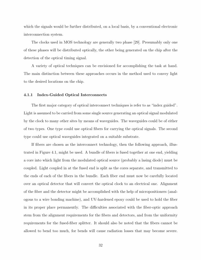
If fibers are chosen as the interconnect technology, then the following approach, illus-
trated in Figure 4.1, might be used. A bundle of fibers is fused together at one end, yielding
a core into which light from the modulated optical source (probably a lasing diode) must be
coupled. Light coupled in at the fused end is split as the cores separate, and transmitted to
the ends of each of the fibers in the bundle. Each fiber end must now be carefully located
over an optical detector that will convert the optical clock to an electrical one. Alignment
of the fiber and the detector might be accomplished with the help of micropositioners (anal-
ogous to a wire bonding machine), and UV-hardened epoxy could be used to hold the fiber
in its proper place permanently. The difficulties associated with the fiber-optic approach
stem from the alignment requirements for the fibers and detectors, and from the uniformity
requirements for the fused-fiber splitter. It should also be noted that the fibers cannot be
allowed to bend too much, for bends will cause radiation losses that may become severe.
32
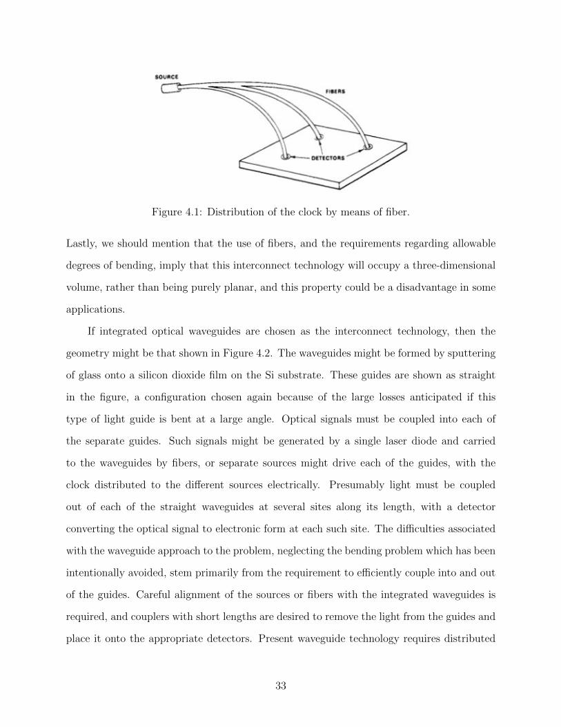
Figure 4.1: Distribution of the clock by means of fiber.
Lastly, we should mention that the use of fibers, and the requirements regarding allowable
degrees of bending, imply that this interconnect technology will occupy a three-dimensional
volume, rather than being purely planar, and this property could be a disadvantage in some
applications.
If integrated optical waveguides are chosen as the interconnect technology, then the
geometry might be that shown in Figure 4.2. The waveguides might be formed by sputtering
of glass onto a silicon dioxide film on the Si substrate. These guides are shown as straight
in the figure, a configuration chosen again because of the large losses anticipated if this
type of light guide is bent at a large angle. Optical signals must be coupled into each of
the separate guides. Such signals might be generated by a single laser diode and carried
to the waveguides by fibers, or separate sources might drive each of the guides, with the
clock distributed to the different sources electrically. Presumably light must be coupled
out of each of the straight waveguides at several sites along its length, with a detector
converting the optical signal to electronic form at each such site. The difficulties associated
with the waveguide approach to the problem, neglecting the bending problem which has been
intentionally avoided, stem primarily from the requirement to efficiently couple into and out
of the guides. Careful alignment of the sources or fibers with the integrated waveguides is
required, and couplers with short lengths are desired to remove the light from the guides and
place it onto the appropriate detectors. Present waveguide technology requires distributed
33

Figure 4.2: Distribution of the clock by means of integrated optical waveguides.
couplers with rather large dimensions (5 um x 1 mm) compared with the feature sizes
normally thought of in electronic IC technology. A major advantage of the integrated optics
distribution system lies in its planar character and the small excess volume it requires. A
disadvantage is the comparatively inflexible geometry dictated by the necessity to avoid large
bends of the waveguides.
4.1.2 Free-Space Optical Interconnects
A second major category of optical interconnects can be referred to as “free-space”
techniques. For such interconnects, the light is not guided to its destination by refractive
index discontinuities, but rather by the laws that govern the propagation of light in free
space. It is helpful to distinguish between two types of free-space interconnect techniques,
“unfocused” and “focused”.
Unfocused interconnections are established simply by broadcasting the optical signals
carrying the clock to the entire electronic chip. One such approach is shown in Figure 4.3. A
modulated optical source is situated at a focal point of a lens that resides above the chip. The
signal transmitted by that source is collimated by the lens, and illuminates the entire chip at
normal incidence. Detectors integrated in the chip receive the optical signals with identical
delays, due to the particular location of the source at the focal point of the lens. Hence in
principle there is no clock skew whatever associated with such a broadcast system. However,
the system is very inefficient, for only a small fraction of the optical energy falls on the
34

Figure 4.3: Unfocused broadcast of the clock to the chip.
photosensitive areas of the detectors, and the rest is wasted. Inefficient use of optical energy
may result in requirements for the provision of extra amplification of the detected clock
signals on the chip, and a concomitant loss of area for realizing the other electronic circuitry
required for the functioning of the chip. Moreover, the optical energy falling on areas of the
chip where it is not wanted may induce stray electronic signals that interfere with the proper
operation of the chip. Therefore, it is likely that an opaque dielectric blocking layer would
be needed on the chip to prevent coupling of optical signals at places where they are not
wanted. Openings in this blocking layer would be provided to allow the optical signals to
reach the detectors. Alternate unfocused interconnection techniques could be imagined that
use diffusers rather than a lens. Note that all such techniques require a three-dimensional
volume in order to transport the signals to the desired locations.
The last category of optical interconnections is free-space “focused” interconnections,
which can also be called “imaging” interconnections. For such interconnections, the optical
source is actually imaged by an optical element onto a multitude of detection sites simulta-
neously. As indicated in Figure 4.4, the required optical element can be realized by means
of a hologram, which acts as a complex grating and lens to generate focused grating com-
ponents at the desired locations. The efficiency of such a scheme can obviously exceed that
35

Figure 4.4: Focused optical distribution of the clock using a holographic optical element.
of the unfocused case, provided the holographic optical elements have suitable efficiency.
Using dichromatic gelatin as a recording material, efficiencies in excess of 99 percent can
be achieved for a simple sine wave grating. When a multitude of focused spots are to be
produced, the efficiency will presumably be lower, but should be well in excess of 50 percent.
The flexibility of the method is great, for nearly any desired configuration of connections
can be realized.
The chief disadvantage of the focused interconnect technique is the very high degree of
alignment precision that must be established and maintained to assure that the focused spots
are striking the appropriate places on the chip. Of course, the spots might be intentionally
defocused, decreasing the efficiency of the system, but easing the alignment requirements.
Thus there exists a continuum of compromises between efficiency and alignment difficulty.
Figure 4.5 illustrates a possible configuration that retains high efficiency but minimizes
alignment problems. The imaging operation is provided by two two-element lenses, in the
form of a block with a gap between the elements. A Fourier hologram can be inserted
between the lenses, and it establishes the desired set of focused spots. The hologram itself
consists of a series of simple sinusoidal gratings, and as such the position of the diffracted
spots is invariant under simple translations of the hologram. The source is permanently fixed
36
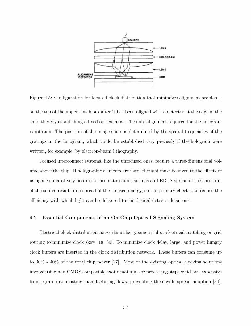
Figure 4.5: Configuration for focused clock distribution that minimizes alignment problems.
on the top of the upper lens block after it has been aligned with a detector at the edge of the
chip, thereby establishing a fixed optical axis. The only alignment required for the hologram
is rotation. The position of the image spots is determined by the spatial frequencies of the
gratings in the hologram, which could be established very precisely if the hologram were
written, for example, by electron-beam lithography.
Focused interconnect systems, like the unfocused ones, require a three-dimensional vol-
ume above the chip. If holographic elements are used, thought must be given to the effects of
using a comparatively non-monochromatic source such as an LED. A spread of the spectrum
of the source results in a spread of the focused energy, so the primary effect is to reduce the
efficiency with which light can be delivered to the desired detector locations.
4.2 Essential Components of an On-Chip Optical Signaling System
Electrical clock distribution networks utilize geometrical or electrical matching or grid
routing to minimize clock skew [18, 39]. To minimize clock delay, large, and power hungry
clock buffers are inserted in the clock distribution network. These buffers can consume up
to 30% - 40% of the total chip power [27]. Most of the existing optical clocking solutions
involve using non-CMOS compatible exotic materials or processing steps which are expensive
to integrate into existing manufacturing flows, preventing their wide spread adoption [34].
37

Figure 4.6: An optical clock distribution system.
A truly CMOS compatible solution will reduce manufacturing cost and facilitate easier inte-
gration into main stream manufacturing. Such an approach was introduced in [38, 40, 53].
Figure 4.6 shows the various stages in an optical clocking system which is compatible with
the proposed approach in [40] and [38]. The optical clock source is optically coupled to the
distribution network, which is optoelectronically coupled to an optical detector that converts
incident optical energy into current pulses. The recovery and signal condition stage then am-
plifies the current pulses to generate a corresponding rail-to-rail electrical clock signal for
local distribution. The clock signal is distributed to the entire chip by dividing the chip
into clock domains and placing a clock recovery resource or transimpedance amplifier (TIA)
station in each domain.
4.2.1 Optical Clock Source
The optical source providing the optical clock is a laser diode that is external to the
chip. The laser diode is attached to a single mode optical fiber. The optical energy at the
end of this fiber is the optical input to the clock distribution network. The optical coupling
into the clock distribution network is achieved by positioning and gluing the fiber to the
polished edge of the die.
38

Figure 4.7: Line diagram of an optical H-tree.
4.2.2 Optical Clock Distribution Tree
On-chip waveguides can be used to construct a planar optical H-tree. A 16 leaf-node,
balanced optical H-tree (as shown in Figure 4.7) is used as the optical clock distribution
network in the on-chip optical clock distribution and recovery system.
Seamless integration of the optical distribution network into standard CMOS processing
is of paramount importance, especially since the distribution network is spatially the largest
component of the system and where the advantages of optical signaling is most pronounced.
The planar waveguide core is constructed from silicon nitride (SiN), which is normally used
for copper encapsulation in a standard CMOS process. The cladding layers are made of
silicon dioxide (SiO2) and low-k oxides such as phospho-silicate glass (PSG) and tetra ethyl
ortho silane (TEOS), normally used as inter-metal dielectric material in standard CMOS
processes. The silicon nitride is deposited using a plasma-enhanced chemical vapor deposi-
tion (PECVD) technique on to a PSG/TEOS/SiO2 sandwich, which serves as the bottom
cladding. The top cladding is a TEOS/SiO2 layer. The high index difference between the
waveguide core and cladding provides excellent optical confinement in the waveguide. To
improve optical coupling between the H-tree and the external optical source, i.e., the optic
fiber, the waveguide core is wider at the die edge and slowly tapered down to the detectors.
39

Figure 4.8: Traveling wave photo detector.
4.2.3 Optical Receiver: Photo Detector
The electrical clock is recovered from the optical clock by using a photo detector which
is placed at the end of each H-tree leaf node. In addition to being truly CMOS compatible,
the photo detector must have high bandwidth and photo sensitivity. Conventional photo
detectors such as P-I-N photodiodes have current “tails” (i.e., long temporal response) in
their time domain impulse response, effectively limiting incident optical energy switching
speed [22]. This behavior is attributed to the thickness of the photo detector and the greater
distance between the electrodes and where the carriers are generated within the detector.
Conventional photo detector designs therefore are insufficient for optical clock distribution
purposes where clock frequencies are high and constantly increasing. A more suitable photo
detector should have high speed and fast impulse response with minimal photo current tail.
A thin polysilicon layer, when used as the detector material, generates carriers in the
high field region with minimal photo current tail. However, a thin polysilicon layer results
in low detector responsivity. Thus, a traveling wave or lateral incidence detector (as shown
in Figure 4.8 [53]), which greatly enhances photo detector responsivity without the need
for thick polysilicon layer, is used. The thin polysilicon layer ensures that the carriers are
generated close to the contacts (electrodes), greatly improving the response time of the photo
detector. Furthermore, for a lateral incidence photo detector with a thin polysilicon layer,
40

Figure 4.9: General approach to optical global clock distribution network.
the photocurrent has lower dependence on the bias voltage as the carriers are generated close
to the contacts and are less likely to undergo recombination.
The lateral incident photo detector, which is placed at the leaf-node of the optical H-
tree, when properly biased generates a current pulse for every incident laser pulse. The
photo detector initiates the clock recovery process by converting the incident optical clock
to current pulses (photo current) which are then processed to generate electrical clock signals
for local distribution. Due to the low magnitude of the photo current, it cannot be used
directly to drive clock sink nodes. A TIA is used to convert, amplify and condition the photo
current to generate rail-to-rail electrical clock signal.
4.3 Comparison of Power Consumption with Electrical Distribution System
Grzegorz et al [49] compare the power consumption of optical and conventional electrical
clock distribution systems. Figure 4.9 shows a low-power vertical cavity surface emitting
laser (VCSEL) used as an off-chip photonic source. The VCSEL is coupled to the H-tree
symmetrical passive waveguide structure and provides the clock signal to N optical receivers.
The number and placement of the receivers in an optical clock system is equivalent to the
41

Figure 4.10: Power consumption of optical and electrical clock distribution networks versusthe number of H-tree nodes.
number and placement of the output nodes in the electrical H-tree. At the receivers, the
high speed optical signal is converted to an electrical signal and subsequently distributed by
the local electrical networks. The number of optical to electrical converters is a particularly
crucial parameter in the overall system since optoelectronic interface circuits at these points
are, ofcourse, necessary and consume power. The methodology and the assumptions used to
properly design the optical H-tree are presented in detail in [47, 48].
First, the power consumption of both systems is compared. The comparison is based
on the ITRS technology roadmap [3] in the case of electrical clock systems and on the state-
of-the-art device parameters in the case of optical clocks. This assumption may result in a
pessimistic estimation of the performance of the optical clock distribution network, for future
technology nodes. The results presented in Figure 4.10 show the comparison between power
consumption of electrical and optical clock systems, both designed for the 70 nm technology
node. For a small number of H-tree nodes the power consumed by the optical H-tree is
more than one order of magnitude lower than in the electrical one. However, along with the
growth of circuit complexity, the advantage of the optical system tends to decrease. Finally,
with 8172 output nodes in the considered case, the power consumed by the optical system
becomes higher than that consumed by the electrical one. This fact can be easily explained
taking into consideration the optical power budget [47, 48]. Along with doubling the number
42

Figure 4.11: Chip structure with temperature gradient.
of H-tree output nodes, the optical power, which needs to be emitted by the VCSEL to meet
the overall system quality increases at least by 3.2 dB, which in turn increases the electrical
power consumed by VCSEL by more than 100%. Additionally, since the number of receivers
is equal to the H-tree output nodes, the power consumed by receivers also doubles. In the
case of an electrical system the power consumption increases much less rapidly. These results
clearly show that the advantages of optics drastically decrease with the number of output
nodes.
In the next step the clock skew of the optical system is calculated. There are several
sources of clock skew in optical system. Apart from process parameter variations, which are
mainly the tolerance of device and waveguide physical parameters, system level fluctuations
like temperature variations have to be considered. In their analysis only the impact of
temperature variation on optical signal speed have been taken into account. Along with the
growth of chip temperature, the refractive index of waveguide core increases, thus reducing
the speed of clock signal. Typical temperature gradients over the entire chip presented in the
literature are less than 50 K [37]. The calculation has been performed for the chip structure
where the temperature of one part is lower (350 K), while that of the other part is higher
(400 K) as presented in Figure 4.11. This represents the worst-case scenario.
43

Figure 4.12: Clock skew of a 64-output-node optical H-tree compared to the clock period asa function of technology.
Figure 4.12 shows the clock skew of a 64-output-node optical H-tree compared to the
clock period as a function of technology. It is clear from this figure that just for the 32 nm
technology node (33 GHz) the clock skew is higher than 10% of the clock period. This will
result in a serious system failure.
4.4 Conclusion
The use of optics to make connections within and between chips could solve many of
the problems experienced in current electrical systems. Many of the physical reasons for the
use of optics are well understood and indicate many potential quantitative and qualitative
benefits. Though there are, and will continue to be, electrical solutions that stretch the
capabilities of electrical interconnects, optics is arguably the only physical solution available
to solve the underlying problems of interconnects, and has the potential to continue to scale
with future generations of silicon integrated circuits.
44
Chapter 5
Future Work
5.1 Wireless Clock Distribution
• External power amplifiers (PAs) are used to increase the power level of the transmitted
clock signal because the on-chip PA is mis-tuned. External PAs increase the system
complexity and increase the cost. They should be replaced by an on-chip PA. In this
system, the transmitted global clock signal is an amplitude-modulated sine wave with
periodic no-signal-transmission, which is generated by switches at output nodes. A PA
with high output power and power efficiency should be designed and fabricated.
• The local clock signal frequency is limited by the operating frequency of clock trans-
mitter and receiver. There is much room for increasing the clock frequency using this
technology. In an inter-chip wireless clock distribution system, microwaves propagate
at the speed of light to distribute the clock signals across a chip. The RC-delay and
dispersion associated with conventional metal-line interconnections are almost elimi-
nated. Using this technology, the maximum local clock signal frequency is set by the
maximum operating frequency of clock transmitter and clock receiver, and the clock
skew and jitter at really high frequencies. According to recent publications, CMOS ICs
using a UMC 0.13um process can reach an operating frequency of ∼100GHz [10, 24].
Therefore, the maximum clock frequency will be limited only by the clock skew and
jitter. As discussed earlier, the skew and jitter performances have the potential of
being excellent, which could give more margin for the clock frequency increase. To
further reduce the clock skew and jitter, the free-running VCO in the clock trans-
mitter should be replaced by a PLL, and a clock receiver with lower noise should be
45

developed. With the increase of clock frequency, the on-chip receiving antenna size
can be reduced, which will reduce the on-chip receiving antenna area, a major problem
in the system. As a result of the smaller receiving antenna size, the width and height
of rectangular apertures in heat sinks can be reduced, which should improve the heat
sink performance.
5.2 Optical Clock Distribution
• Optoelectronic devices require continued development to meet the yield, tolerance,
and drive voltage requirements for practical systems with future generations of silicon
CMOS.
• Work will be required in the interface circuits between optics and electronics. Though
there appears to be no current fundamental difficulty in making such circuits in CMOS,
research is needed in circuits that, i) avoid issues such as crosstalk and susceptibility
to digital noise, ii) have appropriately low power dissipation and latency, and iii) are
tolerant to process variations.
• The technology for integrating optoelectronics with silicon integrated circuits is still
at an early stage, though there have been key demonstrations of substantial working
integrations. Likely first introductions of optical interconnect to chips will use hybrid
approaches, such as solder bonding; such hybrid approaches require no modifications
to the current process for fabricating silicon integrated circuits except to add processes
to fabricated silicon integrated circuit wafers.
• It will be important to research the systems and architectural benefits of optics for
interconnects. Optics can likely enable kinds of architectures that are not well suited
to electrical interconnect systems (e.g., architectures with many long connections, ar-
chitectures with large “aspect ratios,” architectures requiring synchronous operation
over large domains), and can likely also allow continued use of current architectures
46
that otherwise would have to be abandoned in the future because of the limitations of
wired interconnects.
47
Bibliography
[1] “The International Technology Roadmap for Semiconductors,” 1999. Semiconductor IndustriesAssociation, San Jose, California.
[2] “The International Technology Roadmap for Semiconductors,” 2001.
[3] “The International Technology Roadmap for Semiconductors,” 2005.
[4] H. B. Bakoglu, Circuits, Interconnections, and Packaging for VLSI. New York: AddisonWesley, 1990.
[5] K. Banerjee, S. J. Souri, P. Kapur, and K. C. Saraswat, “3-D ICs: A Novel Chip Design forImproving Deep-Submicrometer Interconnect Performance and Systems-on-Chip Integration,”Proc. IEEE, vol. 89, pp. 602–633, 2001.
[6] L. Benini and G. De Micheli, “Transformation and Synthesis of FSMs for Low-Power GatedImplementation,” in Proceedings International Symposium on Low Power Design, Apr. 1995,pp. 21–26.
[7] A. Bhatnagar, Low Jitter Clocking of CMOS Electronics Using Mode-Locked Lasers. PhDthesis, Stanford University, Palo Alto, California, 2005.
[8] W. J. Bowhill, R. L. Allmon, S. L. Bell, E. M. Cooper, D. R. Donchin, J. H. Edmondson,T. C. Fischer, P. E. Gronowski, A. K. Jain, P. L. Kroesen, B. J. Loughlin, R. P. Preston,P. I. Rubinfeld, M. J. Smith, S. C. Thierauf, and G. M. Wolrich, “A 300-MHz 64-b Quad-Issue CMOS RISC Microprocessor,” IEEE Jour. Solid-State Circuits, vol. 30, no. 11, pp.1203–1211, Nov. 1995.
[9] D. Bravo, Investigation of Background Noise in Integrated Circuits Relating to the Design ofan On-Chip Wireless Interconnect System Master’s thesis, University of Florida, Gainesville,Florida, 2000.
[10] C. Cao and K. K. O, “A 90-GHz Voltage-Controlled Oscillator with a 2.2-GHz Tuning Rangein a 130-nm CMOS Technology,” in Symp. VLSI Circuits Dig. Tech. Papers, (Kyoto, Japan),2005.
[11] K.-N. Chen, M. J. Kobrinsky, B. C. Barnett, and R. Reif, “Comparisons of Conventional,3-D, Optical, and RF Interconnects for On-Chip Clock Distribution,” IEEE Transactions onElectron Devices, vol. 51, no. 2, Feb. 2004.
[12] T.-Y. Chiang, K. Banerjee, and K. C. Saraswat, “Effect of Via Separation and Low-k DielectricMaterials on the Thermal Characteristics of Cu Interconnects,” in Proc. IEEE Electron DeviceMeeting, 2000, pp. 261–264.
[13] C. Debaes, A. Bhatnagar, D. Agarwal, R. Chen, G. A. Keeler, N. C. Helman, H. Thienpont,and D. A. B. Miller, “Receiver-Less Optical Clock Injection for Clock Distribution Networks,”IEEE Journal of Selected Topics in Quantum Electronics, vol. 9, no. 2, March/April 2003.
48

[14] A. Deutsch, H. Harrer, C. W. Surovic, G. Hellner, D. C. Edelstein, R. D. Goldblatt, G. A.Biery, N. A. Greco, D. M. Foster, E. Crabbe, L. T. Su, and P. W. Coteus, “FunctionalHigh-Speed Characterization and Modeling of a Six-Layer Copper Wiring Structure and Per-formance Comparison With Aluminum On-Chip Interconnections,” in IEEE Electron DeviceMeeting Tech. Digest, Dec. 1998, pp. 295–298.
[15] D. W. Dobberpuhl, R. T. Witek, R. Allmon, R. Anglin, D. Bertucci, S. Britton, L. Chao, R. A.Conrad, D. E. Dever, B. Gieseke, S. M. N. Hassoun, W. Hoeppner, K. Kuchler, M. Ladd, B. M.Leary, L. Madden, E. J. McLellan, D. R. Meyer, J. Montanaro, D. A. Priore, V. Rajagopalan,S. Samudrala, and S. Santhanam, “A 200-MHz 64-b Dual Issue CMOS Microprocessor,” IEEEJour. Solid-State Circuits, vol. SC-27, no. 11, pp. 1555–1565, Nov. 1992.
[16] B. Floyd, C.-M. Hung, and K. O. Kenneth, “Intra-Chip Wireless Interconnect for Clock Dis-tribution Implemented With Integrated Antennas, Receivers, and Transmitters,” IEEE Jour.Solid-State Circuits, vol. 37, pp. 543–552, 2002.
[17] B. A. Floyd and K. O. Kenneth, “The Projected Power Consumption of a Wireless ClockDistribution System and Comparison to Conventional Distribution Systems,” in Proc. IITC,1999.
[18] E. Friedman, Clock Distribution Networks in VLSI Circuits and Systems. New York: IEEEPress, 1995.
[19] B. A. Gieseke, R. L. Allmon, D. W. Bailey, B. J. Benschneider, S. M. Britton, J. D. Clouser,H. R. F. III, J. A. Farrell, M. K. Gowan, C. L. Houghton, J. B. Keller, T. H. Lee, D. L.Leibholz, S. C. Lowell, M. D. Matson, R. J. Matthew, V. Peng, M. D. Quinn, D. A. Priore,M. J. Smith, and K. E. Wilcox, “A 600-MHz Superscalar RISC Microprocessor with Out-Of-Order Execution,” in ISSCC Dig. Tech. Papers, Feb. 1997, pp. 176–177.
[20] J. W. Goodman, F. Leonberger, S.-Y. Kung, and R. A. Athale, “Optical Interconnections forVLSI Systems,” Proceedings of the IEEE, vol. 72, no. 7, pp. 850–866, July 1984.
[21] X. Guo, D. Yang, R. Li, and K. K. O, “A Receiver with Start-up Initialization and Pro-grammable Delays for Wireless Clock Distribution,” in IEEE Int. Solid-State Circuits Conf.Digest of Tech. Papers, 2006, pp. 386–387.
[22] U. Hilleringman and K. Goser, “Optoelectronic System Integration on Silicon: Waveguides,Photodetectors, and VLSI CMOS Circuits on One Chip,” IEEE Trans. Electron Devices,vol. 42, no. 5, pp. 841–846, May 1995.
[23] M. Horowitz, “Clocking Strategies in High Performance Processors,” in Proceedings of theIEEE Symposium on VLSI Circuits, June 1992, pp. 50–53.
[24] P. Huang, M. Tsai, H. Wang, C. Chen, and C. Chang, “A 114GHz VCO in 0.13um CMOSTechnology,” in Proc. ISSCC, 2005. Paper 21.8.
[25] M. J. Kobrinsky, B. A. Block, J. F. Zheng, B. C. Barnett, E. Mohammed, M. Reshotko,F. Robertson, S. List, I. Young, and K. Cadien, “On-Chip Optical Interconnects,” Intel Tech-nology Journal, vol. 8, no. 2, May 2004.
[26] H. Kojima, S. Tanaka, and K. Sasaki, “Half-Swing Clocking Scheme for 75% Power Saving inClocking Circuitry,” in Proceedings of the IEEE Symposium on VLSI Circuits, June 1994, pp.23–24.
[27] J. Lillis, C.-K. Cheng, and T. Lin, “Optimal and Efficient Buffer Insertion and Wire Sizing,”in Proc. IEEE Custom Integr. Circuits Conf., May 1995, pp. 259–262.
49

[28] S. List, C. Webb, and S. Kim, “3D Wafer Stacking Technology,” in Proc. Advanced Metalliza-tion Conf., Oct. 2002, pp. 29–36.
[29] C. Mead and L. Conway, Introduction to VLSI Systems. Reading, Massachusetts: Addison-Wesley, 1980.
[30] J. Mehta, An Investigation of Background Noise in ICs and Its Impact on Wireless ClockDistribution Master’s thesis, University of Florida, Gainesville, Florida, 1998.
[31] D. Miller, A. Bhatnagar, S. Palermo, A. Emami-Neyestanak, and M. Horowitz, “Opportunitiesfor Optics in Integrated Circuits Applications,” in Proceedings of the International Solid StateCircuits Conference, 2005.
[32] D. A. B. Miller, “Rationale and Challenges for Optical Interconnects to Electronic Chip,”Proc. IEEE, vol. 88, pp. 728–749, 2000.
[33] J. Montanaro, R. T. Witek, K. Anne, A. J. Black, E. M. Cooper, D. W. Dobberpuhl, P. M.Donahue, J. Eno, W. Hoeppner, D. Kruckemyer, T. H. Lee, P. C. M. Lin, L. Madden, D. Mur-ray, M. H. Pearce, S. Santhanam, K. J. Snyder, R. Stehpany, and S. C. Thierauf, “A 160-MHz,32-b, 0.5-W CMOS RISC Microprocessor,” IEEE Jour. Solid-State Circuits, vol. 31, no. 11,pp. 1703–1714, Nov. 1996.
[34] A. Mule, E. Glytsis, T. Gaylord, and J. Meindl, “Electrical and Optical Clock DistributionNetworks for Gigascale Microprocessors,” IEEE Trans. Very Large Scale Integration (VLSI)System, vol. 10, no. 5, pp. 582–594, Oct. 2002.
[35] C. Nagendra and M. J. Irwin, “Design Trade-Offs in CMOS FIR Filters,” in Proc. IEEEInternational Conference on Acoustics, Speech, and Signal Processing Conference, volume 6,May 1996.
[36] J. Neves and E. Friedman, “Circuit Synthesis of Clock Distribution Networks Based on Non-Zero Clock Skew,” in Proceedings of IEEE International Symposium on Circuits and Systems,May/June 1994, pp. 4.175–4.178.
[37] F. J. Pollack, “New microarchitecture challenges in the coming generations of CMOS processtechnologies,” in Proc. 32nd Ann. ACM/IEEE Int. Symp. Microarchitecture, (Haifa, Israel),1999, pp. 2–4.
[38] R. Pownall, G. Yuan, T. Chen, P. Nikkel, and K. Lear, “Geometry dependence of cmos-compatible, polysilicon, leaky-mode photodetectors,” IEEE Photon. Technol. Lett., vol. 19,no. 7, pp. 513–515, Apr. 2007.
[39] P. Ramanathan, A. Dupont, and K. Shin, “Clock Distribution in General VLSI Circuits,”IEEE Trans. Circuits Syst. I: Fundam. Theory Appl., vol. 41, no. 5, pp. 395–404.
[40] A. Raza, G. W. Yuan, C. Thangaraj, T. Chen, and K. Lear, “Waveguide Coupled CMOSPhotodetector for On-Chip Optical Interconnects,” Lasers Electro-Optics Soc., vol. 1, pp.152–153, Nov. 2004.
[41] R. Reif, A. Fan, K.-N. Chen, and S. Das, “Fabrication Technologies for Three-DimensionalIntegrated Circuits,” in Proc. IEEE International Symp. Quality Electronic Design, 2002, pp.33–37.
[42] P. J. Restle and A. Deutsch, “Designing the Best Clock Distribution Network,” in Proc. Symp.VLSI Circuits, 1998, pp. 2–5.
50

[43] W. Ryu, J. Lee, H. Kim, S. Ahn, N. Kim, B. Choi, D. Kam, and J. Kim, “RF Interconnectfor Multi-Gbit/s Board-Level Clock Distribution,” IEEE Trans. on Adv. Packaging, vol. 23,pp. 398–407, 2000.
[44] A. Z. Shang and F. A. P. Tooley, “Digital Optical Interconnects for Networks and ComputingSystems,” Lightwave Technology, vol. 18, pp. 2086–2094, 2000.
[45] I. Sutherland, B. Sproul, and D. Harris, Logical Effort: Designing Fast CMOS Circuits.Morgan-Kaufmann, 1999.
[46] S. Tam, S. Rusu, U. N. Desai, R. Kim, J. Zhang, and I. Young, “Clock Generatition andDistribution for the First IA-64 Microprocessor,” IEEE Jour. Solid-State Circuits, vol. 35, pp.1545–1552, 2000.
[47] G. Tosik, F. Gaffiot, Z. Lisik, I. O’Connor, and F. Tissafi-Drissi, “Optical Versus ElectricalInterconnections for Clock Distribution Networks in New VLSI Technologies,” in Proc. Inte-grated Circuit and System Design, Power and Timing Modeling, Optimization and Simulation,volume 2799, Sept. 2003, pp. 461–470.
[48] G. Tosik, F. Gaffiot, Z. Lisik, I. O’Connor, and F. Tissafi-Drissi, “Metallic Clock DistributionNetworks in New VLSI Technologies,” IEE Electron. Lett., vol. 40, no. 3, Feb. 2004.
[49] G. Tosik, Z. Lisik, and F. Gaffiot, “Optical Interconnections in future VLSI systems,” Journalof Telecommunications and Information Technology, pp. 105–108, 2007.
[50] S. H. Unger and C.-J. Tan, “Clocking Schemes for High-Speed Digital Systems,” IEEE Trans.Computers, vol. C-35, no. 10, pp. 880–895, Oct. 1986.
[51] D. Wann and M. Franklin, “Asynchronous and Clocked Control Structures for VLSI BasedInterconnection Networks,” IEEE Trans. Computers, vol. C-32, no. 3, pp. 284–293, Mar. 1983.
[52] C. Webb, C. J. Anderson, L. Sigal, K. L. Shepard, J. S. Liptay, J. D. Warnock, B. Curran,B. W. Krumm, M. D. Mayo, P. J. Camporese, E. M. Schwarz, M. S. Farrell, P. J. Restle,R. M. A. III, T. J. Slegel, W. V. Huott, Y. H. Chan, B. Wile, T. N. Nguyen, P. G. Emma,D. K. Beece, C.-T. Chuang, and C. Price, “A 400-MHz S/390 Microprocessor,” IEEE J. SolidState Circuits, vol. 32, no. 11, pp. 1665–1675, Nov. 1997.
[53] G. Yuan, R. Pownall, P. Nikkel, C. Thangaraj, T. Chen, , and K. Lear, “Characterization ofCMOS Compatible Waveguide-Coupled Leaky-Mode Photodetectors,” IEEE Photon. Technol.Lett., vol. 18, no. 15, pp. 1657–1659, Aug. 2006.
[54] Q. Zhu and W. Dai, “Planar Clock Routing for High Performance Chip and Package Co-Design,” IEEE Transactions on VLSI Systems, vol. 4, no. 2, pp. 210–226, June 1996.
51