a thesis submitted to the faculty of graduate and ... · providing unique advantages as well as...
TRANSCRIPT

AN ON-CHIP ELECTRICALLY SMALL ULTRA-WIDEBAND ANTENNA IN CMOS
by
William Che Knisely
A thesis submitted to theFaculty of Graduate and Postdoctoral Affairs
in partial fulfillment of the requirements for the degree of
Master of Applied Science in Electrical and Computer Engineering
Ottawa-Carleton Institute for Electrical EngineeringDepartment of Electronics
Faculty of EngineeringCarleton University
Ottawa, Canada
September, 2010
Copyright © 2010 William Che Knisely

?F? Library and ArchivesCanada
Published HeritageBranch
395 Wellington StreetOttawa ON K1A 0N4Canada
Bibliothèque etArchives Canada
Direction duPatrimoine de l'édition
395, rue WellingtonOttawa ON K1A 0N4Canada
Your file Votre référenceISBN: 978-0-494-71512-3Our file Notre référenceISBN: 978-0-494-71512-3
NOTICE: AVIS:
The author has granted a non-exclusive license allowing Library andArchives Canada to reproduce,publish, archive, preserve, conserve,communicate to the public bytelecommunication or on the Internet,loan, distribute and sell thesesworldwide, for commercial or non-commercial purposes, in microform,paper, electronic and/or any otherformats.
L'auteur a accordé une licence non exclusivepermettant à la Bibliothèque et ArchivesCanada de reproduire, publier, archiver,sauvegarder, conserver, transmettre au publicpar télécommunication ou par l'Internet, prêter,distribuer et vendre des thèses partout dans lemonde, à des fins commerciales ou autres, sursupport microforme, papier, électronique et/ouautres formats.
The author retains copyrightownership and moral rights in thisthesis. Neither the thesis norsubstantial extracts from it may beprinted or otherwise reproducedwithout the author's permission.
L'auteur conserve la propriété du droit d'auteuret des droits moraux qui protège cette thèse. Nila thèse ni des extraits substantiels de celle-cine doivent être imprimés ou autrementreproduits sans son autorisation.
In compliance with the CanadianPrivacy Act some supporting formsmay have been removed from thisthesis.
Conformément à la loi canadienne sur laprotection de la vie privée, quelquesformulaires secondaires ont été enlevés decette thèse.
While these forms may be includedin the document page count, theirremoval does not represent any lossof content from the thesis.
Bien que ces formulaires aient inclus dansla pagination, il n'y aura aucun contenumanquant.
1+1
Canada

Abstract
Recent allocation of the Ultra WideBand (UWB) 3.1 to 10.6 GHz frequency spectrum
for unlicensed use has opened many new opportunities for radio communications.
Providing unique advantages as well as interesting design challenges makes UWB an
attractive technology to pursue. Furthering the challenge is the desire to monolith i-
cally integrate an UWB radio with an antenna. Such a feat would reduce manufactur-
ing complexity, while maintaining a high level of cost effectiveness. With these two
technologies in mind, as well as traditional methods, design considerations for the
development of an on-chip ultra wideband antenna in CMOS are discussed. After a
review of current UWB antennas, an electrically small square loop radiator inte-
grated in a 0.13 µp? CMOS process is proposed for use as an UWB antenna. An UWB
LNA and pulse generator are monolithically included with the antenna. Simulation
results of this antenna show it to perform as expected, having a relatively constant,
but poor return loss of less than 1 dB, an omnidirectional radiation pattern, low dis-
persion, and a maximum gain ranging from -25 dBi to -35 dBi over the UWB spec-
trum. Due to complications with the on-chip circuitry, measurements are unable to
confirm the radiation patterns and transient response of the antenna. Despite this,
measurements show the maximum gain is in good agreement with simulation over
the entire band, while the return loss is less than 10 dB, but shows multiple unex-
pected resonances. Phase response of the antenna was linear with an R2 value of
0.99, indicating the antenna may be a good device for use with impulse radios. Al-
though the results are somewhat inconclusive, data does indicate the antenna is still
potentially a viable candidate for use with UWB.
- ii -

Acknowledgements
I would like to thank my supervisor, Calvin Plett, who has been only supportive, as-
sistive, and patient beyond requirement Also, I thank the many students, faculty,
and staff of the Department of Electronics at Carleton University for their assistance,
support, and for this opportunity to learn and grow. Although the credit may be soli-
tary, this thesis was only possible by the actions of a group effort
The financial support of Carleton University and Natural Sciences and Engineering Re-
search Council ofCanada (NSERC) is gratefully acknowledged.
Finally, I wish to thank my spouse for her constant support and encouragement dur-
ing the long hours I spent working towards this milestone in my life and career.
- iii -

Table of Contents
Abstract ¡iAcknowledgements ii¡Table of Contents ¡?List of Tables viList of Figures viiList of Acronyms x
Chapter 1: Introduction 111.1 Ultra-Wideband Communications 12
1.2 On-Chip Antennas 141.3 Thesis Outline 15
Chapter 2: Fundamental, UWB, and CMOS Antenna Design 162.1 Fundamental Antenna Design 16
2.1.1 Near and Far Field 172.1.2 Reciprocity 182.1.3 Radiation Intensity, Directivity, and Isotropic Antennas 192.1.4 Radiation Efficiency and Gain 202.1.5 Equivalent Isotropically Radiated Power 222.1.6 Antenna Impedance, Matching, and Bandwidth 222.1.7 Antenna Effective Aperture 262.1.8 Polarization 262.1.9 Radiation Pattern 272.1.10 Half Power Beamwidth 302.1.11 Antenna System Overview 30
2.2 Ultra-Wideband Communications 322.2.1 UWB Signal Generation 332.2.2 UWB Antenna Considerations 34
2.3 CMOS Integrated Circuits .362.3.1 CMOS Structure 362.3.2 CMOS Integrated Antennas 38
Chapter 3: Current UWB and On-Chip Antennas 413.1 CMOS On-Chip Antennas 423.2 UWB Antennas 43
3.2.1 Multiple Resonance Antennas 433.2.2 Traveling Wave Antennas 453.2.3 Frequency Independent Antennas 463.2.4 Self Complementary Antennas 473.2.5 Electrically Small Antenna s 49
- IV-
3.3 On-Chip UWB Antennas 50
Chapter 4: On-Chip UWB Loop Antenna 524.1 Design 524.2 Simulation 57
4.2.1 Radiation Patterns 584.2.2 Maximum Gain 604.2.3 Return Loss and Input Impedance 614.2.4 Phase and Group Delay „.63
4.3 Measurement 644.3.1 BAE H-1498 Broadband Horn Antenna Reference 664.3.2 Transmitter Measurements 674.3.3 Receiver Measurements 684.3.4 Integrated Antenna Measurements 69
Chapter5: Conclusion 815.1 Conclusion 81
5.2 Future Work 82
References 85
-v-

List of Tables
Table 1. Antenna design parameters. [15] 31
Table 2. The comparison of design considerations for UWB antennas. [9] 35
Table 3. Physical and electrical properties of the CMOS process 54
Table 4. List of test and measurement equipment used to characterise theantenna 65
- vi -

List of Figures
Figure 1-1. FCC and Industry Canada spectral mask for unlicensed indoorUWB emissions 12
Figure 2-1. Radiation pattern of an omnidirectional dipole antenna: (a) 3Dpolar plot, [b) ?-Plane polar plot [directional), [c) ?-Plane polar plot (non-directional) 28
Figure 2-2. Radiation pattern of a directional antenna: (a) 3D polar plot, (b)?-Plane polar plot, [c) ?-Plane polar plot 29
Figure 2-3. An example radiation pattern showing HPBW 30
Figure 2-4. Antenna specification flow chart. [15] 31
Figure 2-5. General profile of CMOS microchip 37
Figure 2-6. Lumped component circuit model of an inductive deviceintegrated in a CMOS process 38
Figure 3-1. The compact uniplanar monopole antenna of [31] 45
Figure 3-2. An exponential Vivaldi antenna with a Marchand balun feed lineon the backside [shown in shadow). This example, taken from [8] is 75 ? 78mm2 46
Figure 3-3. Examples of self complementary antennas: [a) logarithmic spiralantenna and [b) octagonal bowtie antenna 48
Figure 4-1. Chip layout of a small square loop antenna, UWB LNA, and UWBpulse generator, including probing/power pads. Colours indicate the variousmetal layers in the CMOS process, as well as highlight some features andcircuitry as indicated by the legend 55
Figure 4-2. Micro laser cuts and input trace network for combining andseparating the Tx, Rx, and antenna circuits. The green and orange squaresrepresent dummy fill metal. Note: two cuts are not shown, which are locatedto the right and remove the lines going to the probing pads for operation ofthe LNA and pulse generator 57
Figure 4-3. 3D radiation patterns at various frequencies: (a) 3.1 GHz, (b) 7GHz, and [c) 10.6 GHz 59
-vii -

Figure 4-4. Normalized 2D radiation patterns at various frequencies: (a) 3.1GHz, [b) 7 GHz, and (c] 10.6 GHz 60
Figure 4-5. Maximum gain of the antenna for each simulation at variousfrequencies 61
Figure 4-6. Simulated return loss (Sn) of the lossy antenna with and withoutinterfering structures 62
Figure 4-7. Simulated input impedance of the lossy antenna with and withoutinterfering structures 63
Figure 4-8. Simulated phase response with linear fit and group delay of thelossy antenna 64
Figure 4-9. Gain profile of the reference horn antenna 66
Figure 4-10. Shown is a photo of an example of a test setup using a probingstation, an RF probe and mount, and the horn reference antenna. The smallsquare loop antenna is not visible, but located directly under themicroscope's objective 70
Figure 4-11. Measured transmission path gain of the antenna and a GSG RFprobe at a distance of 12 cm 71
Figure 4-12. Corrected antenna maximum gain measured by spectrumanalyzer compared to the simulated gain for a lossy substrate withinterfering structures from Figure 4-5 72
Figure 4-13. Measured and normalized 2D radiation patterns sketches atvarious frequencies: (a) 3.1 GHz, (b) 7 GHz, and (c) 10.6 GHz 74
Figure 4-14. Measured S-parameters using network analyzer connecteddirectly to the antenna 75
Figure 4-15. Input impedance of the antenna calculated from Sn 76
Figure 4-16. Smith chart graph of the simulated and measured Sn parameterof the antenna 77
Figure 4-17. Corrected antenna gain measured by network analyzercompared to the simulated gain for a lossy substrate with interferingstructures from Figure 4-5 79
- vin -

Figure 4-18. Measured phase response and group delay 80
- IX -

List of Acronyms
ADL - Artificial Dielectric LayerCMOS - Complementary Metal-Oxide-SemiconductorEIRP - Equivalent lsotropically Radiated PowerFCC - Federal Communications Commission (United States)Fl - Frequency IndependentGSG - Ground-Signal-GroundHFSS - High Frequency Structure Simulator (Ansoft)HPBW - Half Power BeamwidthIC - Integrated CircuitIEEE - Institute of Electrical and Electronics EngineersUWB-IR - Ultra Wideband Impulse RadioLNA - Low Noise AmplifierMOS - Metal-Oxide-SemiconductorOFDM - Orthogonal Frequency-Division MultiplexingPCB - Printed Circuit BoardPSD - Power Spectral DensityRF - Radio FrequencyRx - Receiver or ReceptionSC - Self ComplementaryTW - Traveling WaveTx - Transmitter or TransmissionUSA - United States of AmericaUWB - Ultra-WidebandVCO - Voltage Controlled OscillatorVLSI - Very Large Scale IntegrationVSWR - Voltage Standing Wave RatioWLAN - Wireless Local Area Network
-x -
Chapter 1: IntroductionThe "era of long-distance radiocommunications was born" in 1901, ushered in by
the first cross Atlantic transmission of an electromagnetic signal [I]. Pioneered by
Guglielmo Marconi, this accomplishment led to the first commercial trans-Atlantic
radio telegraphy service in 1907 [1] and the awarding of a Nobel Prize in 1909 [2],
recognizing wireless communications as both an industrial and academic success
from its inception.
Modern wireless communications have evolved greatly beyond the first telegraphy
systems, in both technical complexity and application. Improvements in coding and
modulation techniques have increased efficiency, allowing greater amounts of in-
formation to be transmitted over a given bandwidth. Advancements in electrical cir-
cuitry have allowed devices to become smaller and smaller, with greater complexity,
yet facilitate mass production while remaining cost effective. Modern wireless
communication devices have become compact, generally affordable, and more po-
werful with each generation of development, leading to a near ubiquitous presence.
A key component to the circuitry of any radio is the antenna. This thesis looks to in-
vestigate the development of an antenna using the combination of two technologies:
Complementary Metal-Oxide-Semiconductor (CMOS) Integrated Circuits (ICs) and
Ultra-Wideband (UWB) pulsed signal generation. Although neither of these areas
are considered new, the combination of each to integrate a wideband antenna has
only recently been considered.
-11-

-12-
1.1 Ultra-Wideband Communications
In February, 2002 the Federal Communications Commission (FCC) of the United
States of America (USA) authorized the unlicensed use of UWB emissions in the 3.1
to 10.6 GHz range [3]. This change has led to an enthusiastic renewal of interest in
UWB radio as it can be favourable for several reasons, including low power high da-
ta rate transmissions, accurate ranging, interference rejection, and coexistence with
narrow bandwidth systems [4] .
-40 ?
-45 4
TT -50 H
E?¦o
•55
¿a. -60C?O
Sj -653oa.
-70
-75 1
-80
---------- FCC
~ ~ Industry Canada
10 11 120123456789Frequency (GHz)
Figure 1-1. FCC and Industry Canada spectral mask for unlicensed indoor UWBemissions.
Utilizing such a large frequency band, UWB operates at a relatively low Power Spec-
tral Density (PSD) of 41.3 dBm/MHz. This specification is required to avoid possible

-13-
interference with narrow band signals that may also be present in the UWB range.
Additionally, greater restrictions are present outside the 3.1 to 10.6 GHz range in
the USA [5] and the 4.75 to 10.6 GHz range in Canada [6]. The FCCs and Industry
Canada's spectral requirements for indoor UWB emissions are shown in Figure 1-1.
The specifications lead to an interesting and unique challenge for UWB design, as
not only is wideband operation required, but also a well defined spectral shape. This
has a large impact on a broad selection of research, including signal generation,
transmission, propagation, processing, and system engineering. Even with these
challenges, many opportunities for novel and effective solutions to the design prob-
lems featured in UWB are permitted, three promising areas of application already
being identified: short range high data rate communications, low data rate sensor
networks with ranging and geo-location, and high resolution radar systems [4].
Antenna design is substantially impacted by UWB. Maintaining a reasonable effi-
ciency and impedance match over such a large bandwidth becomes difficult, while
transient response, typically not a concern, becomes an important issue [7] [8].
UWB antenna development is not as straightforward as narrowband antenna devel-
opment, which is relatively mature and well understood. Given the potential benefit
to applications, but the complexities added by UWB, design of an UWB antenna pi-
ques a great interest [9].

-14-
1.2 On-Chip AntennasIntegration, in electronics and electrical engineering, refers to the monolithic devel-
opment of circuitry in a single medium, typically a semiconductor. This amalgama-
tion of electrical components is motivated by the desire to simplify construction,
lower costs, and reduce the size of electronic circuits, goals that have been amazing-
ly successful [10]. The pervasive presence of electronics owes its existence to the
integration of just about every circuit necessary to create such devices, in particular
the analog circuits necessary for radios [H].
Despite its great success, integration is not a perfect art Strongly linked to the ma-
terial science of semiconductors [12], the performance of ICs has boundaries limited
by the characteristics of the semiconductor in which the circuits are integrated. Ad-
ditionally, the ability, or lack of, to physically manipulate these materials into the
forms required can limit performance. This leads to incongruous ICs, not all compo-
nents being integrated into a single monolithic circuit for performance reasons, and
stimulates research focused on the development of truly monolithic electronic de-
vices.
As a key component of any radio, antennas are traditionally found 'off-chip' due to
two main factors: size and material properties. It is common that at least one di-
mension of a resonant antenna's size is on the order of one wavelength of the fre-
quency of operation, which can be several orders of magnitude greater than the IC
itself. Thus, for many applications, to place an antenna 'on-chip' requires special
consideration and the use of miniaturization techniques. Additionally, the electrical

-15-
characteristics, such as substrate losses and surface wave effects, of the IC can nega-
tively impact an integrated antenna's performance. These factors, too, require spe-
cial design considerations.
Given the great advantages that integration brings to any electrical circuit, it be-
comes obvious why having an antenna on-chip would be favourable, despite the
challenges presented. With a successful design, incorporating an antenna into an IC
would lower production costs and complexity, removing the need for external
transmission line connections and sophisticated packaging. Additionally, an oppor-
tunity is presented to create a multi-purpose element: an antenna that not only
functions as a radiator, but also as an intrinsic component of the circuit itself, able to
provide better matching and more robust capabilities. [13]
1.3 Thesis Outline
After first discussing the motivation behind developing an UWB CMOS integrated
antenna in Chapter 1, this report reviews general antenna design considerations in
Chapter 2. The review includes a look at fundamental antenna design parameters
and characteristics as well as the special exigencies required by UWB and on-chip
CMOS integration. The review is followed by a survey of current UWB antennas, on-
chip CMOS antennas, and UWB on-chip antennas, giving a brief summary of each in
Chapter 3. In Chapter 4, the on-chip UWB loop antenna that was developed for this
thesis is presented. A discussion of the antenna's design, simulation, and measure-
ment is followed by a listing of the results. Finally, in Chapter 5, concluding remarks
are made along with a discussion of the future work required.

Chapter 2: Fundamental, UWB1 andCMOS Antenna Design
The project for this thesis centers on the development of an antenna incorporating
two technologies, UWB pulsed signals and CMOS ICs, for use in a low cost, self con-
tained transceiver. In addition to typical design concerns, special considerations ne-
cessary to implement an antenna in CMOS using UWB must be observed. The vari-
ous technological aspects of the project are discussed below, highlighting these
areas of interest
2.1 Fundamental Antenna DesignAntennas are commonly the first and last component in the signal path of a tran-
sceiver. As such they take an interesting and unique position in the operation of the
radio: unlike the other components, antennas must couple with free -space as well as
the radio's circuitry. This means that antennas require special design considerations
as well as unique characterisations.
The theory of antennas deals mainly with calculations regarding the radiation, into
free space, of electromagnetic fields from a conducting structure and the propaga-
tion of those fields from and to another conducting structure. The various characte-
ristics of antennas are derived from Maxwell's Equations [14] and are paramete-
rized as laid out in the IEEE Standard Definitions of Terms for Antennas [15], some
of which are discussed below.
-16-

-17-
2.1.1 Near and Far Field
The volume surrounding an antenna is broken into two areas: near field and far
field. For the most part, the far field is taken as the more significant as antenna op-
eration is generally at large distances. The following parameters are usually deter-
mined for the far field case. Even so, in cases where the transmitting and receiving
antennas may be close it is important to determine if near field affects may be
present. To this end the two areas are given as follows.
The far field is defined as the region where the radiated angular field distribution is
effectively independent of the distance, r, from the antenna. In free space, this dis-
tance is estimated as:
where a is the maximum overall dimension of the antenna and ? is the wavelength.
This is commonly only valid for cases where a is large compared to ?, otherwise the
more general condition is for a distance where r » ?. It can be shown that, in the far
field, the electromagnetic fields are transverse, always approximated by plane
waves in a local area, and the power is real, being completely dissipative.
The near field is found between the antenna and the far field and is broken into two
parts: radiating and reactive. The reactive portion is found near the antenna, the vo-
lume for which is estimated as r < ?/2p for very short dipole, or similar, antennas.
Within the reactive region, the power is mainly imaginary and thus implies stored

-18-
energy. The radiating region fells between the reactive region and the far field, hav-
ing an angular field distribution that is dependent on the distance, r, from the an-
tenna. Together, with the power being complex, this makes the electromagnetic
fields in the near field non-intuitive and difficult to predict Antennas that are small
compared to the wavelength may not exhibit a radiating near field.
2.1.2 Reciprocity
Reciprocity refers to the characteristics of an antenna remaining unchanged wheth-er that antenna is used as a transmitter or receiver. The transmitting radiation pat-
terns of a given antenna are identical to the receiving radiation patterns, as are the
input impedances and other parameters. This has practical application in that only
one design or measurement (transmit or receive] is necessary to develop or charac-
terize an antenna.
It is important to note that reciprocity is not applicable in all cases. It is generally
true for narrow band passive antennas that the frequency domain transmit and re-
ceive characteristics will be the same, but it is common for UWB antennas, as well as
some other antennas, such as ferrite core antennas, to have differing time domain
transmit and receive characteristics. For example, it is typical for some UWB anten-
nas to act as a differentiator, displaying a signal at the receiver that is the differen-
tial ofthat which was transmitted.

-19-
2.1.3 Radiation Intensity, Directivity, and Isotropic Antennas
The main purpose of an antenna is to direct energy through space. Thus it is impor-
tant to ascertain how an antenna prefers to guide energy to or from one direction
over another. This is accomplished using radiation intensity and directivity.
The total power radiated by an antenna is given by:
P1. = î Ke {JJ (E ? H *).ds}, (2.2)where E is the electric field and H is the magnetic field radiated and the integral is
over a surface in the far field surrounding the antenna. For simplicity the surface is
typically taken as a sphere. Recalling the electromagnetic fields are localized TEM
plane waves in the far field:
Pr=|Äe{J|(EeH;-EipH5)r2du}J (2.3)where dß = Sin ? ?? ?f, an element of a solid angle. It then becomes opportune to
define the radiation intensity of the antenna as:
?(?,f) =-fie{(ExH*)r2}, (2.4)
which is the power radiated, in a given direction, {ß, f), per unit solid angle in units
of watts per square radian.

-20-
Given the radiation intensity, it becomes relatively straightforward to describe the
directivity of an antenna as:
, ^ U(6, f)?(?,f)=-^-^, [2.5]^ave
the ratio of the radiation intensity in a given direction to the average radiation in-
tensity from all directions. The average radiation intensity is simply:
U = — C2.6)Uave 4p- «- J
Maximum directivity, the directivity in the direction of maximum radiation intensi-
ty, is commonly implied using D without ? and f. Directivity is reciprocal.
To further illustrate the concept of directivity, it is convenient to imagine a lossless
antenna, called an isotropic radiator, for which the radiation intensity is equal in all
directions. Generally, an equivalent isotropic radiator emits the same total power as
supplied to an antenna. Thus an isotropic radiator has constant radiation intensity,
Uave, and a directivity of 1. Such an antenna does not practically exist, but it is a use-
ful conceptual reference for highlighting the directive properties of an antenna.
2.1.4 Radiation Efficiency and Gain
The power accepted into the antenna is not equal to the power radiated due to loss
effects in the antenna. Thus the antenna has a radiation efficiency given by:

-21-
e=-^;0<e<l. (2.7)*i rin
Radiation efficiency does not include losses from polarization or impedance mis-
matches. Combining equations (2.5), (2.6), and (2.7), the directivity of an antenna
can then be expressed:
4p?(?,f)D (?, f) = ^. (2.8)
The gain of an antenna, for a given direction, is defined as the ratio of the radiation
intensity of the antenna to the radiation intensity of an equivalent isotropic radiator
or:
4p?(?,f)G(6,cp) = . (2.9)'in
From equations (2.8) and (2.9) it is seen:
G(0,cp) =e?(?,f) (2.10)
Thus it is noted that the gain of antenna is a directional characteristic of the antenna
and proportional to the directivity by the radiation efficiency. Similar to directivity,
maximum gain, the gain in the direction of maximum directivity, is commonly im-
plied using G without ? and f. It is also common to express gain in decibels, denoted
dBi to indicate it is relative to an isotropic radiator.

-22-
2.1.5 Equivalent Isotropically Radiated Power
Equivalent Isotropically Radiated Power (EIRP) is the radiated power an isotropic
radiator would emit to produce the same radiation intensity as that of an antenna in
a given direction. This is expressed by:
EIRP = PinG(0,(p). (2.11)
Since EIRP includes gain and losses between the circuitry and the antenna, it is a
convenient parameter to use when comparing various antennas. EIRP is typically
implied to be in the direction of maximum gain and is expressed in dBi.
2.1.6 Antenna Impedance, Matching, and Bandwidth
The impedance of an antenna is the impedance measured at the terminals of the an-
tenna and is generally complex. Note that, due to reciprocity, the impedance of an
antenna is referred to as input impedance despite the antenna's use as a transmitter
or receiver.
Input impedance is denoted:
Zin = Rin + jXi„. (2.12)
The reactance of the antenna, Xin, signifies the electromagnetic energy stored in the
near field. This corresponds to the large imaginary part of the electromagnetic fields
near the antenna as discussed in section 2.1.1. Generally, electrically small antennas,
defined as antennas for which D « ?, have large reactive input impedances.
-23-
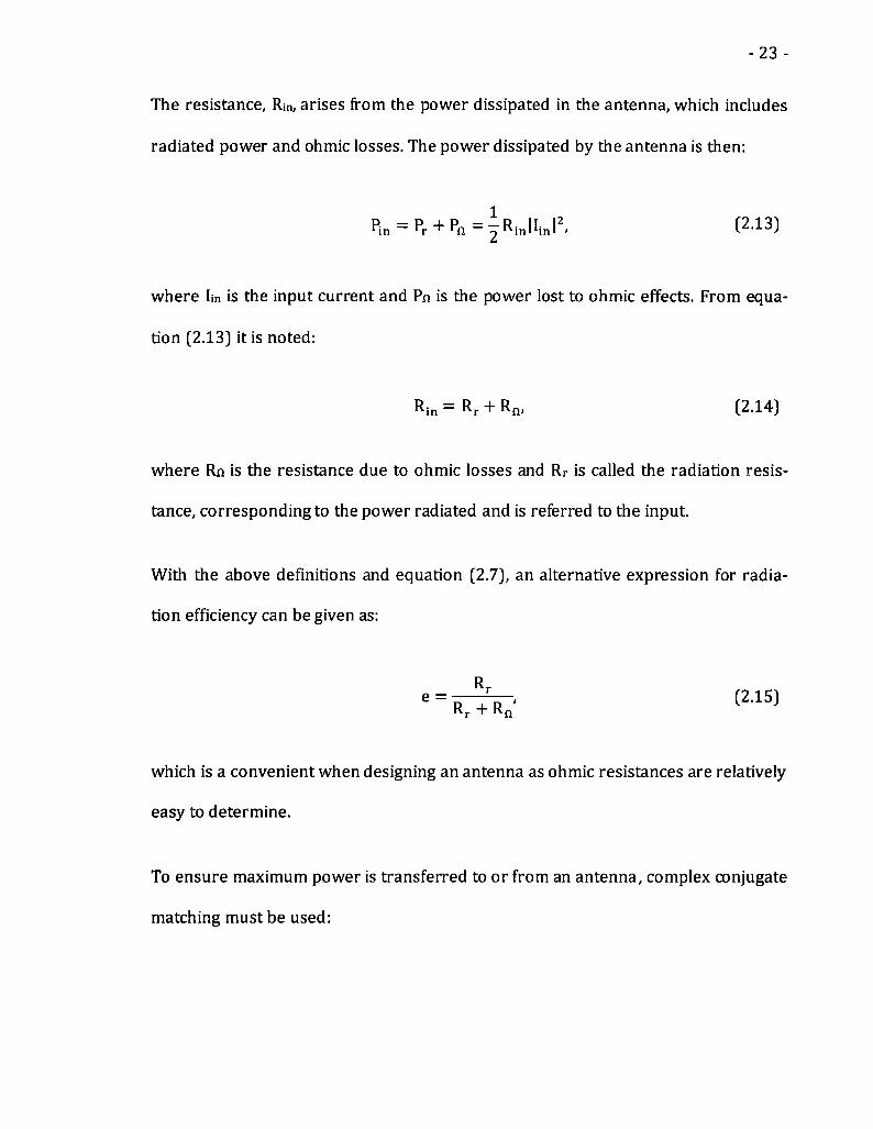
The resistance, Rin, arises from the power dissipated in the antenna, which includes
radiated power and ohmic losses. The power dissipated by the antenna is then:
Pm = Pr + Pn= ^RiJU2- C2.13)where Iin is the input current and Pn is the power lost to ohmic effects. From equa-
tion (2.13) it is noted:
Rin=Rr + Rn, (2.14)
where Rn is the resistance due to ohmic losses and Rr is called the radiation resis-
tance, corresponding to the power radiated and is referred to the input.
With the above definitions and equation (2.7), an alternative expression for radia-
tion efficiency can be given as:
e=iÄ t215)which is a convenient when designing an antenna as ohmic resistances are relatively
easy to determine.
To ensure maximum power is transferred to or from an antenna, complex conjugate
matching must be used:

-24-
Zx = Zfn, (2.16)
where Zx is the input/output impedance of the circuitry connected to the antenna. In
general, a matching network is needed to accomplish this, although it is possible to
design circuits that are intrinsically matched to the antenna.
Mismatches between the circuit of the radio and the antenna can be expressed using
transmission line theory [16]. In the transmitting case, the reflection coefficient, G, is
defined as the ratio between the voltage wave reflected back to the circuitry, V', to
the voltage wave incident on the antenna's terminals, V+. The reflection coefficient
can be expressed as:
V- Zin - ZxG = — = — -. (2.17)V+ Zin+Zx J
It is also of interest to note that the reflection coefficient is also the Sn parameter of
the scattering matrix.
It can then be shown that the power accepted by the antenna is:
Pin=Pi(I-IrI2), (2.18)
where Pi is the power incident on the antenna's terminals. The term(l — |G|2) is
called the impedance mismatch factor, denoted q, while the term |G|2 is called re-
turn loss, expressed in decibels as:

-25-
RL = -20Login, [2.19)
and represents the "loss" of the reflected power. Note, it is common to plot return
loss as its negative.
Another convenient measure of impedance mismatch is the Voltage Standing Wave
Ratio [VSWR). This is a measure of the ratio of the maximum to the minimum volt-
age of the standing wave that arises due to the reflected voltage wave. This is given
as:
V 1+??VSWR = ^x = i^il. (2.20)"min *¦ I* I
The bandwidth of an antenna is specified as the frequency range over which a given
characteristic of the antenna conforms to some specification. Typically, less than
10% reflected power is chosen as the criterion, which corresponds to G = 0.3162.
This is equivalent to RL > 1OdB, typically called the -10 dB bandwidth, and VSWR <
1.92, although this is usually rounded to VSWR < 2.
The fractional bandwidth of an antenna is given as:
B = JLp-k, (2.21)
where fk and fi, are the high and low frequency boundaries of the bandwidth defined
above and fc is the center frequency given by (/H + /L)/2.

-26-
2.1.7 Antenna Effective Aperture
The effective aperture or effective area of an antenna is a measure of its ability to
convert power incident on the antenna to power available at the terminals of the
antenna. It is denoted by:
A6=^G. (2-22)
Effective aperture is a convenient parameter when considering the receiving an-
tenna in an antenna system.
2.1.8 Polarization
The polarization of an antenna is the polarization of the electric far field transmitted
by the antenna in a given direction. Antenna polarization, in general, is elliptical
with special cases where the polarization is circular and linear. Polarization is reci-
procal.
Polarization can affect the power transferred between antennas. Maximum power
transfer for a given direction occurs when two antennas, receiving and transmitting,
are said to have a polarization match. This occurs when, in the same direction, the
receiving antenna has the same polarization as the transmitting antenna. The power
received will be reduced if a polarization mismatch is present To gauge the mis-
match, the polarization efficiency, p, is defined as the ratio of the power received in a
given direction by an antenna from a transmitting antenna of arbitrary polarization

-27-
to that of the power that would be received had the antennas been polarization
matched in the same direction.
2.1.9 Radiation Pattern
A radiation pattern of an antenna is a spatial mapping describing, either graphically
or mathematically, a given characteristic of the electromagnetic field radiated by the
antenna. Typical characteristics used are power flux density, radiation intensity, di-
rectivity, phase, polarization, and field strength [15]. For example, the radiation in-
tensity pattern for an isotropic antenna would appear as a sphere.
Radiation patterns are normally shown graphically and, although 3 dimensional
(3D), 2 dimensional (2D) cuts are common, used to highlight specific features of the
antenna, such as maximum gain in particular planes. For linearly polarized anten-
nas, typical cut planes are the ?-plane and ?-plane. The ?-plane contains both the
electric field vector and the direction of maximum radiation intensity, while the H-
plane contains both the magnetic field vector and the direction of maximum radia-
tion intensity. The ?-pane and ?-plane are orthogonal in the far field. Elevation and
azimuth are also common cut planes, where azimuth is parallel to the earth's surface
(XY plane) and elevation is perpendicular (YZ plane).
Depending on application it may be desirable to have an antenna with a specific type
of radiation pattern. An omnidirectional radiation pattern is one type in which the
pattern is mostly a constant value or non-directional in a given plane and directional
in the orthogonal plane. An isotropic radiator is the ideal omnidirectional antenna,

-28-
although it cannot be realized. Real antennas are always directional in at least one
plane. Omnidirectional antennas are used in applications in which the direction of
the signal transmission is unknown. An example of an omnidirectional radiation
pattern is shown in Figure 2-1.
?—«
*?:. :'-¿
mmm»Vi
\-NS
^
a
0>) (c)Figure 2-1. Radiation pattern of an omnidirectional dipole antenna: (a) 3D polarplot, (b) ?-Plane polar plot (directional), (c) ?-Plane polar plot (non-directional).

-29-
¿m rrW
1^.
Ca)
(b) (e)Figure 2-2. Radiation pattern of a directional antenna: (a) 3D polar plot, (b) E-Planepolar plot, (c) H -Plane polar plot
Other applications may require antennas with a radiation pattern that is highly di-
rective, such as with directional antennas, which radiate or receive more effectively
in various directions than others. An example of a directional antenna is the pencil
beam antenna, the radiation pattern of which contains a single large, main lobe and
several smaller side lobes. Directional antennas are used in applications such as ra-
dar or site to site transmissions. An example of a directional pattern is shown in

-30-
Figure 2-2. There are other categories of radiation patterns, but omnidirectional and
directional are the two main types.
2.1.10 Half Power Beamwidth
Half Power Beamwidth (HPBW) is a measure of the angular size of a lobe in a direc-
tional antenna. Taken in a cut plane containing the maximum of the lobe, it is the
angular measure between the two directions that are half the maximum as seen in
Figure 2-3.
HPBW
3IdBi
12
IS
Figure 2-3. An example radiation pattern showing HPBW.
Note that, for some antennas, such as the omnidirectional type, HPBW is not appli-
cable in some planes.
2.1.11 Antenna System Overview
The various terms from section 2.1 are summarized in Table 1. Additionally, for
each antenna parameter, such as gain and directivity, there is an analogous partial

-31-
parameter. Partial denotes that the effect of polarization mismatch has been taken
into account Also, the overall gain, including impedance mismatches at the antenna
input, is called the realized gain.
Table 1. Antenna design parameters. [15]Ptx = power from the generator.P¡ = power incident on the antenna.P¡n = power accepted by the antenna.Pr = power radiated by the antenna,qi = impedance mismatch between
transmission line and generator.q2 = impedance mismatch between
transmission line and antenna.
e = radiation efficiency of the antenna.
Gr = realized gain of the antenna.G = gain of the antenna.D = directivity of the antenna.gR = partial realized gain of the antenna.g = partial gain of the antenna.d = partial directivity of the antenna.? = polarization efficiency of the system.U = radiation intensity.Un = partial radiation intensity.
Figure 2-4. Antenna specification flow chart. [15]
The terms in Table 1 are represented graphically in Figure 2-4 as the flow of power
from the signal generator to the radiated electromagnetic field of the antenna. Al-
though the chart represents a transmitter, the figure for a receiver would appear

-32-
similar, with the direction of power flow reversed and appropriate variable name
changes, due to reciprocity.
The graph of Figure 2-4 partially represents the Friis transmission equation. The
Friis transmission equation gives an overview of an antenna system made of a
transmitter and a receiver. It is given by:
PRx = PTx + QtxI + Qtx2 + GTx + P + GRx + QrxI + QRx2 + Ppl» (2.23)
where each variable is in dB or dBm, Prx is the power at the receiving load, and Ppi
represents the free space path loss and is given by:
Ppl = 20Lo510(^;) dB, (2.24)where ? is the free space wavelength and r is the distance between the transmit and
receive antennas. The free space path loss represents the reduction in power densi-
ty due to geometrical expansion of the traveling wave as it expands spherically from
the transmitter and the frequency dependency of the receive antenna's effective
aperture. The Friis transmission is a convenient method for specifying antenna sys-
tems.
2.2 Ultra-Wideband Communications
An UWB system is defined as one in which the -10 dB bandwidth is 500 MHz or
greater or the fractional bandwidth is 0.2 or greater [5] [6]. In general, this is much
larger than a narrow band system, which is usually on the order of a few MHz. In

= 33 =
addition, given this large frequency space, UWB systems can make use of 'carrier-
less' signals unlike narrow band transmissions, as well as other novel methods to
transmit information.
2.2.1 UWB Signal Generation
Other than PSD, there is no strict specification as to how the bandwidth in UWB is to
be used, leading to the evolution of various signal modulation techniques [4]. The
various methods can be categorized as Frequency Hopping (FS), Time Hopping
(TH), and Direct Sequence (DS). A fourth method is to use multi-channel conven-
tional modulation schemes at high data rates, an example being Orthogonal Fre-
quency Division Multiplexing (OFDM).
Frequency hopping involves the use of multiple carrier frequencies at various times.
In FH, a known user code is used to 'spread' the carrier frequency over time slots.
For a given time slot, the system transmits at one frequency, then, in a different time
slot, switches to a different frequency as determined by the spreading code algo-
rithm. The length of the time slots can vary from system to system, including conti-
nuous carrier changes, called chirp signaling. The bandwidth of FH is determined by
the frequency range of the carriers used and not the data rate. The main advantage
of FH is interference avoidance allowing multiple users in the same spectrum [17].
Direct sequence schemes modify the original signal by multiplying it by a much
higher rate pseudo-randomly generated sequence of 1 and -1. Since the code se-
quence is higher in frequency, it has the effect of spreading the original signal over a
-34-
wider frequency band and, thus, the rate of the code determines the bandwidth
used. The advantages of DS include resistance to interference (narrow band, multi-
user, or intentional jamming], as well as multipath issues.
OFDM creates a wideband spectrum by virtue of combining many orthogonal nar-
rowband sub-carriers over a range of frequencies. Data can then be transmitted us-
ing various multi-channel coding schemes where each sub-carrier can operate at a
lower rate, but the overall effect is a high rate. Similar to FH, OFDM's bandwidth is
determined by the frequency range of the sub -carriers. Like other UWB schemes,
OFDM is robust to interference, but can give a better spectral efficiency. [18]
Time hopping utilizes impulse radios and, thus, is considered a carrier -less tech-
nique. Data is transmitted by way of sequences of very short duration pulses, which
are compressed in time, but wide in frequency. The spectrum and bandwidth of the
system are controlled by the shape and duration of the pulses. Since the signal is
carrier-less, TH transmitters are generally lower in complexity and consume less
power.
2.2.2 UWB Antenna Considerations
Irrespective of the type of the UWB system being considered, an UWB antenna must
function over the large, 3.1 to 10.6 GHz, bandwidth. Generally, the band of operation
is taken as the antenna's impedance bandwidth, measured by return loss or VSWR.
However, the other antenna parameters, as discussed in section 2.1, must also suf-
fice for the desired application and band of operation. For example, it is typically

-35-
preferred that gain [directivity) and polarization have a constant response over the
entire band. This goal does not differ from narrow band designs, except that for
UWB the difficulty is increased for such a wide range of frequencies.
In addition, for pulse based modulation, such as that in TH schemes, special consid-
erations are necessary. In these instances the antenna acts not only as a radiator,
but also as a bandpass filter, shaping the spectrum of the signal, in some cases even
acting as a differentiator. This can lead to distortions in the pulse shapes, making
reception and detection difficult, and possibly causing failure of the radio if not ac-
counted for. Thus, the transient response and group delay of the antenna become
important considerations. The design aspects of UWB antennas are summarized in
Table 2. [7], [9]
Table 2. The comparison of design considerations for UWB antennas. [9]Constituent MB-OFDM
S wide impedance bandwidthcovering all operating sub-bands
•S steady radiation patternsS constant gain at directions of in-
terest
S constant desired polarizationS high radiation efficiencyS constant desired polarization¦S high radiation efficiency
Pulse Based
Electrical
S wide impedance bandwidthcovering the bandwidthwhere majority of the sourcepulse energy falls in
S constant gain at desired direc-tions
S linear phase responseS constant desired polarizationS high radiation efficiency
Mechanical
S small size / low profile/embeddable /easy-integrated for portabledevices
S compact but robust especially for fixed devicesS low cost

-36-
2.3 CMOS Integrated CircuitsThere are several different types of integration, typically differentiated by the semi-
conductor used. For Radio Frequency (RF) analog circuits conventional choices are
Silicon Bipolar (Si-bipolar) and Gallium Arsenide (GaAs), which generally have very
good high frequency performance. Even so and more recently, CMOS has become a
popular option for RF circuits, its performance in some cases matching or exceeding
that of the traditionally 'faster' processes due to aggressive downscaling [19].
The development of CMOS integration processes has been mostly driven by the digi-
tal electronics field [20]. As such, CMOS has become a widespread and highly devel-
oped integration process, although mainly focused on digital applications. Yet, as the
high frequency performance of CMOS has increased, foundries have made analog
design libraries available. CMOS analog development can be attractive due to the
low cost, ease of manufacture, and compatibility with digital CMOS. The latter is an
exciting advantage, opening possibilities for mixed analog/digital ICs.
2.3.1 CMOS Structure
The profile of a CMOS IC is shown in Figure 2-5 and is made up of 3 general layers,
the substrate, the oxide, and the passivation. Within each general layer, various oth-
er structures are created using lithographic techniques.

-37-
Passivation
Oxide
Substrate
Figure 2-5. General profile of CMOS microchip.
CMOS devices are created in a planar fashion, starting with the substrate and depo-
siting each subsequent layer, using lithography, up to the passivation. This method
requires many steps, including adding and removing numerous intermediate layers.
Active devices are found in the substrate, near the oxide boundary. The various
metal layers, for creating traces and other conducting structures, are contained
within the oxide layer. The passivation is a final layer added to provide protection
from corrosion and physical damage.
The substrate of a silicon integration process is simply modeled as a resistance in
parallel with a capacitance to ground. This represents the lossy coupling of signals
to the substrate, which has a low resistivity. Using lumped elements to represent the
various electrical parameters, one model for an inductor is shown in Figure 2-6. Be-
ing a lumped element model of a continuous effect, more accuracy can be achieved
by repeating the circuit, although one may be sufficient for narrow bands.

38
ln-<
Oxide
>ln+
Oxide
Figure 2-6. Lumped component circuit model of an inductive device integrated in aCMOS process.
2.3.2 CMOS Integrated Antennas
From the perspective of an integrated antenna, the main interest falls on the physi-
cal and electrical properties of the 3 general layers shown in Figure 2-5. To remain
cost effective, it is necessary to fabricate the antenna using the materials found in
mainstream CMOS processes [13]. It is the physical structure and properties of
these materials that present the first limitations and determine overarching restric-
tions on the development and performance of an integrated antenna.

-39-
Being a planar technology, CMOS is most suited to the use of planar structures. To
remain in the paradigm of mainstream CMOS development, the type of antenna used
must also be planar. Additionally, the overall size of the antenna must be small, on
the order of millimeters, as large ICs are difficult to produce and experience low
yields, thus increasing cost. This means, for frequencies in the 3.1 to 10.6 GHz range,
electrically small, non-resonant antennas must be used.
Mainstream CMOS processes use a silicon substrate with a resistivity in the range of
10 - 20 Hem. The lossy substrate negatively impacts the antenna's ability to radiate
power efficiently. In this respect it is prudent to isolate the antenna from the sub-
strate as much as possible, both in distance and by using shielding. Thus it is com-
mon to realize the antenna in the top metal layer and use bottom metal layers to
form grounded shields. Top metal layers also tend to have the lowest resistivity,
thus reducing ohmic losses in the metal. The fabrication process may also allow oth-
er methods to increase substrate resistivity, normally used for increasing electrical
isolation and reducing substrate noise.
Perhaps the most difficult concern to address is that of structural interferers, al-
though with careful design the effects can be minimized [21]. Conducting structures
near the antenna can affect its performance, most notably the impedance and gain.
This is at odds with the desire to integrate an antenna with a radio in as small an
area as possible, which would require placing circuitry near the antenna. In addition
to circuit metallization, CMOS processes require dummy metal structures to fill
empty areas in order to keep the various planes of the layers level. Although it has

-40-
been shown in some instances that dummy fill has a minimal effect on antenna gain
and matching for wireless interconnections, this has not been shown to be similar
for off-chip communications [21].
Chapter 3: Current UWB and On-Chip Antennas
There exist an unlimited number of antennas as any conducting structure can ra-
diate electromagnetic fields. Unfortunately, the performance required of an antenna
is application specific and not all radiators will fit the necessary specifications. A
good example is that of UWB and integrated antennas.
The main physical constraints in such antennas are due to the realization of an an-
tenna in the CMOS integration process. The antenna must be small, possibly non-
resonant depending on the required frequency of operation, and planar. The elec-
trical characteristics of the materials used for integration will also affect the perfor-
mance of the antenna.
Using an antenna in UWB applications sets the required behavioural properties of
the antenna, which in turn influence the shape and structure of the radiator. The de-
sign must be matched over a wide frequency range, while also provide a linear
phase response and good transient characteristics. The gain of the antenna in the
required directions must also be sufficient and as constant as possible over the
band.
By combining both UWB and CMOS integration, the possible types of radiators that
will operate sufficiently are reduced even more. Various candidates are presented
below.
-41-

-42-
3.1 CMOS On-Chip Antennas
Although the aspiration to integrate antennas on-chip is not new, it is only relatively
recent that the techniques necessary to produce such devices in a widespread and
cost efficient manner have come into being. As operating frequencies increase (and
the corresponding resonant antenna sizes decrease) with the development of main-
stream high speed CMOS processes, the ability to fabricate truly monolithic single-
chip radios has become a feasible possibility. This is especially highlighted by recent
worldwide unlicensed use of the 60 GHz (V) band for high data rate, short range
communications. [22]
Current CMOS radios are typically small, on the order of millimeters per side, and
can be found operating in various frequency bands, including UWB or millimeter
wave frequencies. This generally means that integrating antennas on-chip is more
feasible at high frequencies, where the wavelength of the frequency of operation is
similar to the IC size and antenna radiation efficiency is increased [23]. Even so ex-
amples of on-chip antennas can be found ranging in operation from a few GHz to
more than 60 GHz.
An overview of the simulation of several types of antennas integrated in CMOS is
shown in [22]. Here it is shown that although the antennas are approximately of re-
sonant size, substrate losses still play a major role in the gain and efficiency of the
antennas. Additionally, placement of the antenna, near the corner, the side, or the
center of the IC, also plays a role in the radiation characteristics. It was found that
Yagi-Uda type antennas have the best directionality, while a rhombic style radiator

-43-
has the highest gain, and a loop antenna has almost the same gain, but using much
less space.
Two examples of on-chip integrated antennas operating within the UWB spectrum
are found in [24] and [25]. Both antennas are electrically small narrowband loops,
the first operating at 5.2 GHz with a size of 1 x 1 mm2 and the second operating at
2.5 GHz with a size of 1.62 ? 1.62 mm2. As expected, the gains of both antennas are
very poor due to the antenna size and the lossy substrate (see Section 3.2.5 below
and Section 2.3.2 above), but acceptable for short range communications. In both
designs the choice of a loop antenna was made to allow use of the area inside the
loop for circuitry, making a more compact IC, although in [24] the antenna also dou-
bles as an inductor.
3.2 UWB Antennas
The distinguishing mark of UWB antennas is the wide range of frequencies over
which they must operate. To accomplish this there are many kinds of UWB antenna
designs, which can be categorized as: multiple resonance, traveling wave, frequency
independent, self complementary, and electrically small [8]. It is not uncommon for
an antenna to fall into more than one group. Additionally, having an UWB range of
operation does not guarantee that an antenna will meet all required specifications.
3.2.1 Multiple Resonance Antennas
Multiple resonance antennas achieve a wideband response by combining several
narrow band radiators into one structure. Since there are effectively an unlimited

-44-
number of radiators, multiple resonant antennas can take a multitude of shapes and
sizes.
One common type of multiple resonant antennas is the log periodic monopole/ di-
pole array. Here a series of radiating elements, monopole or dipole antennas, whose
sizes and spacings decrease logarithmically, are combined. The log periodic antenna
discussed in [8] shows a fairly constant gain pattern over the UWB frequency range,
although it is not unidirectional. Unfortunately, this antenna does not produce a
good impulse response as a large amount of ringing is evident This is directly attri-
buted to the various resonating elements of the antenna, which introduce frequency
dependent non-linear phase responses. Log periodic antennas in general do not
produce UWB radiators with a good transient response [26].
The elliptical monopole antenna is another UWB radiator that has also been shown
to have multiple resonance characteristics [27], [28]. Despite this, it has also been
shown, with optimization of the major and minor axes of the ellipse, the ground
plane, and the feed line, that not only is a wideband impedance match possible, but
also an excellent transient response [29], [30]. This is due to the use of smooth
transitions, such as those seen in traveling wave structures (see below). A novel ex-
ample of such a monopole, with good UWB performance, is shown in [31]. Another
particular feature of interest of this antenna is its relatively compact size, measuring
30.5 x 38.1 mm2, which is small for a printed circuit.

-45-
a
Figure 3-1. The compact uniplanar monopole antenna of [31].
3.2.2 Traveling Wave Antennas
A Traveling Wave (TW) structure can be thought of as the counterpart to a resonant
antenna. Resonances are standing wave patterns caused by reflections from discon-
tinuities in the structure of an antenna. By smoothing discontinuities, resonances
can be avoided. This is accomplished by using continuously tapered transitions,
usually from the feed point to the end of the antenna, and tends to create a wide-
band response.
The Vivaldi antenna, an example shown in Figure 3-2, is a good illustration of an
UWB tapered wave guide antenna [8]. An antipodal variation of a Vivaldi antenna is
shown in [32]. Both Vivaldi antennas display a directional radiation pattern, but
have a gain that is constant over the UWB frequency range. Additionally, the tran-
sient characteristics show the Vivaldi is suitable for pulsed signal transmission, al-
though its impulse response is not constant with direction.

-46-
Figure 3-2. An exponential Vivaldi antenna with a Marchand balun feed line on thebackside (shown in shadow). This example, taken from [8] is 75 x 78 mm2.
3.2.3 Frequency Independent Antennas
Frequency Independent (FI) antennas offer the prospect of a radiator that is infinite-
ly wideband. Unfortunately, this also requires that the antenna also be infinite, such
as that of the infinite biconical antenna [14]. Even so it is possible to design a prac-
tical antenna that performs almost constantly over a given band.
The concept of FI antennas is derived from the observation that if a radiating struc-
ture is scaled in size, that its characteristics are the same if the input signal's wave-
length is also scaled by the same factor. Thus, if an antenna's shape is independent
of scaling, it is also independent of frequency. This leads to a class of antennas
whose shapes are specified entirely by angles, defined by:
r= ea(<p+ipo)F(0), (3.1)

-47-
where r, f, and ? are the usual spherical coordinates, a is a constant, f? is an angu-
lar constant, and F(G) is any function of T. [33]
The planar equivalent of the biconical antenna is the bowtie. An aperture coupled
bowtie antenna, measuring approximately 36 ? 36 mm2, is shown in [8]. This an-
tenna displays an omnidirectional radiation pattern and reasonable gain. It also has
excellent transient characteristics with little ringing. Of particular interest is that the
impulse response is fairly constant with direction.
A variation of the bowtie antenna, called a rounded diamond dipole antenna is
shown in [34]. This antenna rotates the two fans of the bowtie so that a diamond
shape is created. It is noted that the bandwidth of the frequency response of the
rounded diamond is greater than that of a simple bowtie antenna. Another diamond
dipole antenna, optimized for a better VSWR over the UWB band, is shown in [35].
3.2.4 Self Complementary Antennas
A common subset of FI antennas are Self Complementary (SC) antennas, although
being self complementary in itself does not necessarily guarantee constant radiation
characteristics with frequency [36]. These SC radiators are distinguished by having
metal and dielectric patterns that are the same shape and rotationally displaced,
two examples shown in Figure 3-3.

-48-
(a) (b)Figure 3-3. Examples of self complementary antennas: (a) logarithmic spiral anten-na and (b) octagonal bowtie antenna.
Following Babinef s Principal, the impedance of a self complementary antenna is
given by:
_ _ ?^metal — ^dielectric — ~y ??·*·)
where ? = ^µ/e is the intrinsic impedance of the medium (« 120p for free space).Frequency independence of the impedance is the main feature of SC antennas. This
impedance can be varied by changing the ratio of the metallization to the dielectric,
although the impedance will not remain independent of frequency.
Another self complementary spiral antenna is the Archimedean spiral. Compared to
the continuously increasing line width and spacing of the logarithmic spiral of Fig-
ure 3-3a, the Archimedean spiral has a constant line width and spacing. In either
case, both antennas radiate circularly polarized fields, requiring pulses of sufficient

-49-
length to encompass 360° of the radiated field. Additionally, spiral antennas tend to
introduce dispersion into wideband pulses as lower frequencies are radiated further
from the center, thus causing a frequency dependant delay. [8]
3.2.5 Electrically Small Antennas
An electrically small antenna, sometimes called a non-resonant antenna, is defined
as an antenna whose largest absolute dimension, a, is small compared to the wave-
length, ?, at the frequency of operation [15]. Thus, for an UWB antenna to be electr-
ically small over the entire band, its largest dimension must be much smaller than
the wavelength of a 10.6 GHz signal, which, in free space, is a « 28.2 mm.
An alternate definition for an electrically small antenna is given by:
ka < 1, (3.3]
where k is the wave number, given byk = 2p/? [37]. This leads toa < 4.5 mm as
the boundary for an UWB antenna to be electrically small over the entire band. Al-
though any antenna can be scaled down to become small, various types of antennas
lend themselves to this task more easily. Monopoles, dipoles, loops, and their deriva-
tives are common choices [8].
Non-resonant antennas display wideband behaviour by performing "equally bad"
over the UWB spectrum [8]. Since these antennas are electrically small, it is ex-
pected that the radiation characteristics, such as maximum achievable gain, will be
adversely affected [38], [39], but in a relatively constant manner and somewhat in-
-50-
dependent of frequency. Additionally, small antennas typically present an input im-
pedance that can be highly reactive, making UWB input impedance matching diffi-
cult [40], [41], [37].
A miniaturized antenna, approximately 20 x 20 mm2, is shown in [42]. Operating at
a frequency of approximately 910 MHz, this antenna uses a split ring resonator to
cancel the large inductance of the small loop antenna, making impedance matching
much easier. Unfortunately this also has the effect of making the antenna narrow
band, but otherwise achieves reasonable gain and efficiency for its small size.
Some examples of small UWB antennas can be found, but are typically not consi-
dered electrically small for the entire UWB spectrum [43], [44], [45].
3.3 On-Chip UWB AntennasGiven that, separately, UWB and CMOS integrated antennas present various issues
in design and performance, it is not surprising that it is difficult to find an example
that combines both technologies. Placing an UWB antenna on-chip requires either a
very large IC, which can be cost prohibitive, or using an electrically small antenna,
which degrades radiation characteristics. In both cases, substrate losses will affect
performance unless some sort of mitigating technique is provided.
Reference [46] shows a monolithically integrated dipole antenna with an RF front
end, including a Low Noise Amplifier (LNA) and a mixer. This device has an imped-
ance bandwidth over the UWB spectrum and was designed for use with OFDM ap-
plications. The antenna achieves a gain of approximately -20 dBi, but transient cha-

-51-
racteristics were not measured as that is not required for OFDM applications. Even
so, it is assumed that, because this design uses a multiple resonant structure, tran-
sient response is most likely poor. In addition, the antenna designed is quite large,
measuring 10 x 0.67 mm2, although remains less than the wavelengths of the fre-
quencies in the UWB spectrum.
Another UWB fully integrated RF front end is shown in [47] with an antenna and an
LNA. The antenna is a folded inverted-F with size 4.5 x 3.5 mm2, which approaches
an electrically small antenna for the UWB spectrum. Additionally, to combat the
losses caused by the low resistivity substrate, an Artificial Dielectric Layer (ADL) is
placed under the antenna, but above the substrate. The ADL increases the effective
permittivity and shields the antenna from the lossy substrate. Use of the ADL was
not demonstrated to be overly effective as the antenna gain was approximately -30
dBi over the UWB, but theory predicts an ADL with greater permittivity could im-
prove this. Use of the ADL introduces a tradeoff between antenna performance and
chip space as circuitry cannot be placed under an ADL. Transient characteristics
were not measured, but due to the resonant features of this antenna it is expected
they are poor.

Chapter 4: On-Chip UWB Loop An-tenna
When integrating monolithic radiators, the small size of ICs dictates the use of elec-
trically small antennas in the UWB spectrum. This, combined with the losses due to
a low resistivity substrate, all but guarantees poor gain and efficiency. Thus, the
choice of topology for an on-chip UWB antenna integrated in CMOS is somewhat ar-
bitrary from a performance point of view. Even so, practical applications can still be
found for such antennas and therefore the topology used can be determined by oth-
er factors, such as minimizing the overall IC area and, thus, reducing cost
Monopoles, dipoles and loops are common types of antennas that are often found in
a below-resonant size. As shown in Section 3.1 and 3.3, it is feasible to integrate
these kinds of antennas in a CMOS process and operate them over UWB frequencies.
For this thesis a square loop antenna was chosen to be implemented as discussed
below.
4.1 DesignThe main constraint on the antenna's topology is determined by the IC size. For this
design an overall chip size of approximately 1.5 x 1.5 mm2 is assumed, sufficient
space for a small loop antenna, the UWB LNA designed by Ansari [48], and the UWB
pulse generator designed by Salehi-Abari [49]. By using a loop antenna to circum-
scribe the circuitry, a large antenna compared to the above given chip size is at-
tained without rendering the entire area unusable to other circuitry. In addition to
-52-

-53-
maximizing the useful area on-chip, loop antennas are also preferred for applica-
tions where the radio is located near obstructions, such as in hand -held or body
worn devices. This is due to the fact that loop antennas have a mainly magnetic reac-
tive field, and thus are less susceptible to de-tuning by any local high dielectric con-
stant materials.
The IC was fabricated in a CMOS 0.13 µ?? process, seen in Figure 4-1. The antenna is
fabricated in the top layer metal, shown in blue, and is made of aluminum. Various
other metal layers are also shown in other colours, which are mainly seen as power
feed lines from the pads located around the right and top of the antenna. These met-
al layers are found within the oxide layer of the process, while the top metal layer,
except for the pads, is covered in the passivation.
Use of the CMOS 0.13 µ?? process sets the material properties which will physically
and electrically constrain the design, shown in Table 3. It is noted that the effective
relative permittivity of the structure is a weighted average of the three layers and
somewhere between 4 and 11.9. In addition, the fabrication process also allows for a
special means for increasing the resistivity of the substrate in selected locations. The
technique used to accomplish this is unknown, as is the exact final resistivity. De-
spite this, any increase in the substrate's resistivity is expected to improve the an-
tenna's performance and is therefore implemented on the substrate beneath the an-
tenna (outlined by the dotted orange line as seen in Figure 4-1).

-54-
Table 3. Physical and electrical properties of the CMOS process.
Layer Resistivity(ilcm)
ConductivityCS/m)
ErHeight(µp?)
Substrate 13.5 7.407 11.9 300
Oxide OO 0 16.72
Passivation OO 7.9
The antenna was made as large as possible, while allowing for ample spacing of the
probe landing/power pads and circuitry, and also remaining electrically small over
the UWB spectrum. The outer circumference was set to 1mm per side. The line
width was simulated from 10 µp? to 250 µp? in parametric analysis simulation. The
results showed the radiation characteristics had little variation over the widths, but
the input impedance did change. The input resistance increased with decreasing
width, while the inductive reactance increased at a greater rate. A line width of 100
µp? was chosen to reduce the lossy effect of the increased resistance, but still remain
small enough to fit the LNA and pulse generator within the antenna's loop.
The final dimensions of the antenna give a mean circumference of 3.8 mm. For an
ideal small loop antenna with an equivalent circumference and an effective relative
permittivity mentioned in the paragraph above, the resonant frequency would be
expected to be between 22.8 GHz and 39.5 GHz. Such an antenna, having ka < 1, can
be considered an electrically small antenna over the entire UWB spectrum.

55
min
A
o
High resistivity boundaryUWB LNA
3UWB Pulse Gen.
M7 {Top metal layer} M5M4
Figure 4-1. Chip layout of a small square loop antenna, UWB LNA, and UWB pulsegenerator, including probing/power pads. Colours indicate the various metal layersin the CMOS process, as well as highlight some features and circuitry as indicated bythe legend.
Inclusion of both an UWB LNA for reception (Rx] (the LNA's capacitors and spiral
inductors can be seen in the center of the antenna in Figure 4-1, surrounded by a
light blue dashed line) and a pulse generator for transmission (Tx) (seen right of the

-56-
LNA and above the antenna's tapered feed lines in Figure 4-1, surrounded by a red
dashed line) requires the use of a small network of traces for micro laser cutting,
shown in Figure 4-2. Additionally, traces to connect the antenna to probing pads for
off-chip measurements are included. Micro laser cutting uses a high powered, highly
focused laser to cut through the IC. In doing so, small incisions can be made to sepa-
rate the Tx, Rx, and antenna for individual testing, while allowing all three to be in-
tegrated on the same IC. Although the use of the traces for micro laser cutting may
complicate the antenna feed line, it is unavoidable without sacrificing 2 of the three
designs as chip space is limited.
Unlike typical designs, the antenna feed lines are directed inward, since the LNA and
pulse generator are located within the loop. The feed lines are elliptically tapered
along a 90° bend to facilitate a wideband impedance transition from the antenna to
the circuitry. Although, at these electrically small sizes, using tapered impedance
matching may prove ineffective, it should not hamper performance and may avoid
unwanted resonances, similar to that discussed in Section 3.2.2 without adding
great complexity.
The LNA and pulse generator are placed within the loop antenna such that the input
of the LNA and the output of the pulse generator are as close to the feed lines as
possible. Since the LNA is not differential, one side of the antenna's feed lines is
grounded, while the other side is connected to the LNA input (noted as gnd. and RFin
respectively in Figure 4-2). The pulse generator drives a differential signal (noted as

-57-
pulse+ and pulse- in Figure 4-2} and therefore presents no problems connecting to
the antenna.
MM· mMicro Laser Cut Line HHH
useTrace Network ¦¦¦ HHHH
l_JH
HHHHHBA : Cuts for LNAB : Cuts for Pulse Gen
HHH HHHCuts for Probe PadsWm
HHHHHHHHH HHHHHHHHHHI WMa
BB
?
BRFi
HHI¦
!!I
Figure 4-2. Micro laser cuts and input trace network for combining and separatingthe Tx, Rx, and antenna circuits. The green and orange squares represent dummy fillmetal. Note: two cuts are not shown, which are located to the right and remove thelines going to the probing pads for operation of the LNA and pulse generator.
4.2 Simulation
The antenna was laid out and simulated using Ansoft High Frequency Structure Si-
mulator (HFSS). HFSS is a full-wave 3D electromagnetic simulator that can provide
"E- and ?-fields, currents, S-parameters and near and far radiated field" for any
geometry [50]. For this project HFSS was used to design, simulate, and numerically

-58-
determine the S-parameter, impedance, and radiation characteristics of the loop an-
tenna discussed in Section 4.1.
The simulations were conducted using a 1.5 ? 1.5 mm2 substrate with the heights
and electrical properties presented in Table 3. The antenna structure is imple-
mented on the top metal layer, made of aluminum, and is centered on the substrate
with the x-axis in the direction of the feed lines, the y-axis in the direction of the
pads, and the z-axis up, out of the passivation (corresponding to the right, up, and
out of the page respectively in Figure 4-1). The antenna is differentially driven,
across the two feed lines, with a 50 O sinusoidal 1 volt source.
3 simulations were performed: a lossless (0 conductivity) substrate with the an-
tenna alone, a lossy substrate with the antenna alone, and a lossy substrate with
metal interference structures (pads, etc.). In the lossless simulation the maximum
gain and radiation patterns were calculated. In the two lossy simulations the maxi-
mum gain, radiation patterns, return loss, input impedance, phase, and group delay
were calculated.
4.2.1 Radiation Patterns
The radiation patterns for each of the 3 simulations were created for three frequen-
cies: 3.1 GHz, 7 GHz, and 10.6 GHz. The radiation patterns for the simulations are
shown in Figure 4-3 (3D) and Figure 4-4 (2D). It was noted that for the 3 simula-
tions all were similar in shape, having negligible differences. The patterns are omni-

-59-
directional in the XY-plane, parallel with the antenna, as is expected for a small radi-
ating loop. It is also noted that the pattern begins to bow inwards along the y-axis,
^ÊÊÊ^
a (b)
ss
a
(C)Figure 4-3. 3D radiation patterns at various frequencies: (a) 3.1 GHz, (b) 7 GHz, and(c) 10.6 GHz.
perpendicular of the feed lines on the x-axis, as the frequency increases. This is ex-
pected, as, at resonant frequencies, the loop antenna's omnidirectional radiation
pattern would change to become perpendicular to the plane of the loop (omnidirec-
tional in the XZ-plane) [14].

-60-
XY-Plane-30 30 30 301 XZ-Pane
YZ-Pane
?-60 60 -60 60\y
/
-so 90 -30 90
\
/
120 120-" 120 120^
150 150 150 150
L_JISO 180
Ca) OO30 30
XY-PlaneXZ-Pane
-40 60 YZ-Plane
^ \S \
\\
90 90
/s
S
120 120
150 150
Figure 4-4. Normalized 2D radiation patterns at various frequencies: [a] 3.1 GHz, (b)7 GHz, and (c) 10.6 GHz.
4.2.2 Maximum Gain
Figure 4-5 shows how the maximum gain is variable as a function of frequency and
the substrate resistivity, but is negligibly affected by interfering structures placed
around and inside the antenna. As expected, in all cases, the gain of the small loop
antenna is very poor and made worse by the lossy substrate, but does improve with
frequency as the antenna approaches resonance. In addition, the effect of the lossy

-61-
substrate increases with frequency as shown by the increase in the difference b e-
tween the gains of the lossy and lossless cases. This is as expected as coupling to the
substrate, modeled as a resistance in parallel with a capacitance, increases with fre-
quency.
-10
-12
-14
-16
-18
¦Lossless Substrate
¦Lossy Substrate (No Structures)
Lossy Substrate (With Structures)
a -28ID
6 7 8
Frequency (GHz)10 11
Figure 4-5. Maximum gain of the antenna for each simulation at various frequencies.
4.2.3 Return Loss and Input Impedance
The return loss of the lossy simulations is shown in Figure 4-6. As expected, the
match between the antenna and the 50 O voltage source is very poor, but only varies
by about 0.5 dB over the UWB spectrum. The calculated input impedance of the an-
tenna, modeled as a series resistance and inductance, is shown in Figure 4-7. Similar

-62-
to the radiation patterns, the inclusion of interfering structures has a minor effect on
the impedance and matching of the antenna.
-0.4
-0.5
-0.6
(?«?
5-0.7C
3
atoc
No Structures
With Structures
-0.8
-0.9
-1
6 7 8Frequncy (GHz)
10 11
Figure 4-6. Simulated return loss (Sn) of the lossy antenna with and without inter-fering structures.

-63-
45
Resistance No Structures40
2.8Resistance With Structures
35
Inductance No Structures30
**Inductance With Structures? 25 ?
re re
!£20inO ir 2.1 "O
15 m
u,**
?? ?1.8
*A>**¦j,**^
3456789 10 11
Frequency (GHz)Figure 4-7. Simulated input impedance of the lossy antenna with and without inter-fering structures.
4.2.4 Phase and Group Delay
Figure 4-8 shows the simulated phase and group delay. Although the phase is not
linear, it is close having a linear regression R2 value of 0.971. This translates to a
group delay range from about 15 ps at 10.6 GHz to 52 ps at 3.1 GHz, a variance of
approximately 37 ps. Compared to the antennas discussed in Chapter 3:, this is a
small value.

-64-
Phase-+- G roup Delay
6 7 8Frequency (GHz)
10
60
55
50
h 45
40«=
y= -9.6431X+ 129.44R2 = 0.971
11
Figure 4-8. Simulated phase response with linear fit and group delay of the lossy an-tenna.
4.3 Measurement
Measurement of antenna characteristics are generally performed using equipment
such as network analyzers, spectrum analyzers, signal generators, and reference an-
tennas with known characteristics. Standard measurements include gain, radiation
patterns, impedance, bandwidth, beamwidths, and polarization. These parameters,
especially the radiation characteristics, are typically done in an anechoic chamber to
remove reflected signals and avoid multi-path issues. A list of the equipment used to
perform measurements for this project is shown in Table 4.
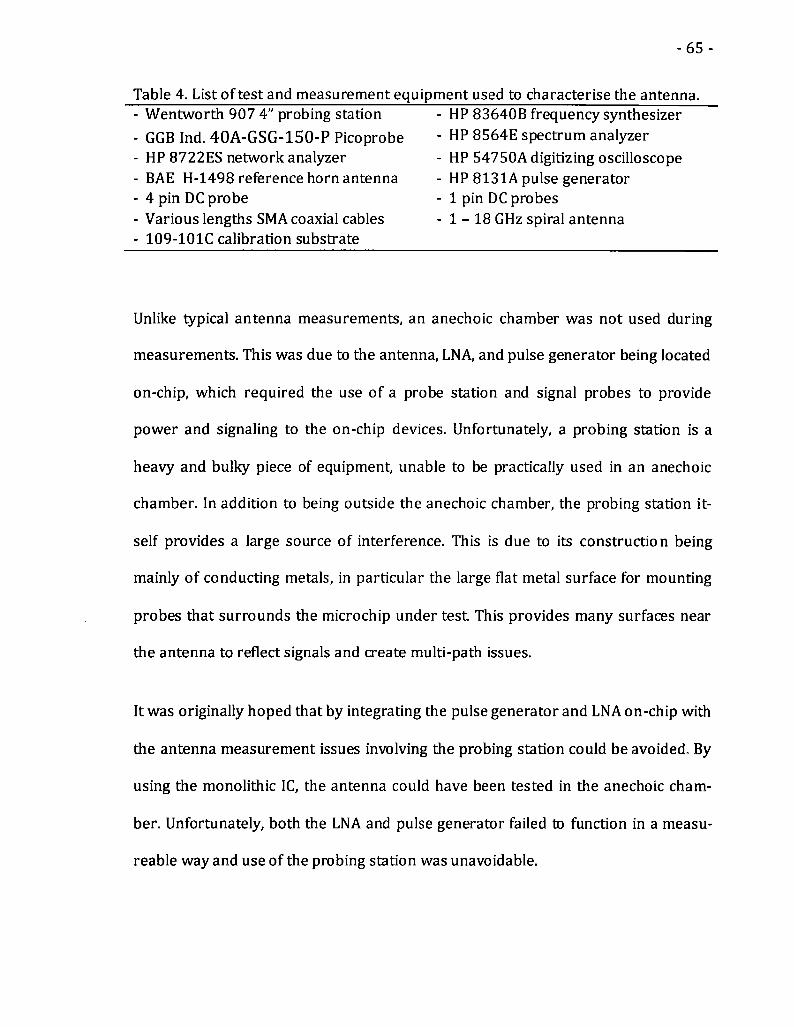
-65-
Table 4. List of test and measurement equipment used to characterise the antenna.- Wentworth 907 4" probing station - HP 83640B frequency synthesizer- GGB Ind. 40A-GSG-150-P Picoprobe - HP 8564E spectrum analyzer- HP 8722ES network analyzer - HP 54750A digitizing oscilloscope- BAE H-1498 reference horn antenna - HP 813 IA pulse generator- 4 pin DC probe - 1 pin DC probes- Various lengths SMA coaxial cables - 1 - 18 GHz spiral antenna- 109-101C calibration substrate
Unlike typical antenna measurements, an anechoic chamber was not used during
measurements. This was due to the antenna, LNA, and pulse generator being located
on-chip, which required the use of a probe station and signal probes to provide
power and signaling to the on-chip devices. Unfortunately, a probing station is a
heavy and bulky piece of equipment, unable to be practically used in an anechoic
chamber. In addition to being outside the anechoic chamber, the probing station it-
self provides a large source of interference. This is due to its construction being
mainly of conducting metals, in particular the large flat metal surface for mounting
probes that surrounds the microchip under test This provides many surfaces near
the antenna to reflect signals and create multi-path issues.
It was originally hoped that by integrating the pulse generator and LNA on-chip with
the antenna measurement issues involving the probing station could be avoided. By
using the monolithic IC, the antenna could have been tested in the anechoic cham-
ber. Unfortunately, both the LNA and pulse generator failed to function in a measu-
reable way and use of the probing station was unavoidable.

-66-
4.3.1 BAE H-1498 Broadband Horn Antenna Reference
Before measurements can be conducted, the radiation parameters of the reference
antenna are needed. The BAE H-1498 is a linearly polarized broadband double
ridged horn antenna. It has a VSWR better than 2 over its operating range of 2 to 18
GHz, matching it to 50 Ü. The gain profile of the antenna versus frequency is shown
in Figure 4-9.
12
11.5
11
10.5 ?
Cu
"??U)
10
9.5
8.5
8
3 4 5 6 7 8
Frequency (GHz)Figure 4-9. Gain profile of the reference horn antenna.
10 11
A second wideband spiral antenna was used in conjunction with the spectrum ana-
lyzer and frequency synthesizer to confirm that transmission and reception of sig-
nals from the horn antenna reference was working.

-67-
4.3.2 Transmitter Measurements
To test the IC as a transmitter, the pulse generator and antenna circuit was utilized.
The IC was mounted on the probing station and the 2 power pins were supplied via
DC probes. A third DC probe was used to connect the on-chip pulse generator's trig-
ger to the HP 8131A pulse generator. A 1 to 1.5 MHz square wave was used to set
the pulse repeating frequency of the on-chip pulse generator. The reference horn
antenna was connected to the HP 54750A digitizing oscilloscope, which used the
external trigger supplied directly from the HP 8131A pulse generator. The transmit-
ted pulse from the on-chip loop antenna could not be detected.
In addition to the above setup, the IC was also mounted on a Printed Circuit Board
[PCB) and connected to drive the pulse generator through wire bonds. This was
originally done to use the transmitter in the anechoic chamber, but ultimately no
pulses could be detected. Despite this, useful experience was garnered involving
PCB mounting and wire bonding.
A third testing method was also attempted by connecting a known working pulse
generator of the same design from off-chip. This required the use of two RF probes
and several DC probes. Unfortunately, the generated pulse was too greatly atte-
nuated by the probes to be usable.
The exact reasoning for the device failure is not known, although troubleshooting
seems to indicate a problem with signal propagation between the circuitry and the
antenna. Measurements of the DC power draw of the UWB pulse generator indicate

-68-
that it is functioning. Increasing the pulse rate increases the DC current draw as ex-
pected, signifying pulses are being generated, but no detectable transmitted signal
can be found. Although it is still possible that the pulse generator is failing to create
a signal, it is more likely that the pulses are attenuated beyond measurability due to
impedance mismatches as the pulse generator is designed to differentially drive a
50 Í1 load, while the on-chip loop antenna has a mainly (simulated) inductive im-
pedance over the UWB band, seen in Figure 4-7 and Figure 4-16. This highlights one
of the key issues with using electrically small antennas; impedance matching can be
difficult due to the relative low real and high reactive impedance components.
4.3.3 Receiver Measurements
To test the IC as a receiver, the UWB LNA and antenna circuit was utilized. The IC
was mounted on the probing station and the 3 power pins were connected using a 4
pin DC probe. A Ground-Signal-Ground (GSG) RF probe (GGB Ind. 40A-GSG-150-P
Picoprobe) was used to connect the RFout on the UWB LNA to the HP 8564E spec-
trum analyzer. The HP 83640B frequency synthesizer was connected to the refer-
ence horn antenna and used to radiate continuous signals at various frequencies at
an input power of approximately 12 dBm. The on-chip antenna was illuminated
with signals from 3 to 11 GHz, but no signal could be detected on the spectrum ana-
lyzer.
Similar to the on-chip pulse generator, troubleshooting the LNA seems to indicate a
problem with matching. The LNA, having a maximum return loss of -7.5 dB over the

-69-
UWB spectrum, was designed with a 50 O input impedance. It is most likely that the
signals are attenuated beyond measurability due to impedance mismatching.
4.3.4 Integrated Antenna Measurements
Although unable to use the integrated UWB pulse generator and UWB LNA, and,
thus, the anechoic chamber, the antenna was measured directly while mounted on
the probing station. Using a GSG probe, the antenna was driven by landing one of the
ground pins on one antenna feed line and the signal pin on the other antenna feed
line. The second ground pin was landed on a dummy pad. Two setups were used
with the antenna driven in this manner: the first involving the frequency synthesizer
and the spectrum analyzer, while the second used the network analyzer.
A measurement setup is shown in Figure 4-10. Using this setup, the antenna under
test and the horn reference antenna can be connected either to a spectrum analyzer
and frequency generator or a 2 -port network analyzer. For radiation pattern mea-
surements, the microscope can be removed from the probing station, although the
probe and various parts of the probing station will still present obstacles.
4.3.4.1 Antenna Measurements Using Spectrum Analyzer
The first setup connected the antenna, via GSG RF probe, as a receiver to the spec-
trum analyzer, while the frequency synthesizer was connected to the horn antenna
reference for transmitting. The horn antenna was then fixed a distance of 12 cm
from the IC in the -X direction in the XY-plane as this is theoretically the direction of

-70-
Figure 4-10. Shown is a photo of an example of a test setup using a probing station,an RF probe and mount, and the horn reference antenna. The small square loop an-tenna is not visible, but located directly under the microscope's objective.
maximum radiation. The radiated signal was then swept over 3 to 11 GHz and the
power level from the on-chip loop antenna recorded. The procedure was then re-
peated with the probe raised above the pads to measure any radiation from the

-71-
probe. A final measurement was then made to calibrate the input power at each fre-
quency and account for losses in the cables.
From Figure 4-11 it is seen that the RF probe contributes very little to the transmit-
ted signal. The signal from the probe is 23.2 dB below the signal from the antenna
on average and is always less than 11.5 dB. The other feature of note is the variance
of the power level of the received signal. This is most likely due to multi-path losses
from reflections off the probing station.
.2 -50
Q- -60
-65
-70
-75
-¦—Measured Power
*¦ Probe
6 7 8Frequency (GHz)
10 11
Figure 4-11. Measured transmission path gain of the antenna and a GSG RF probe ata distance of 12 cm.
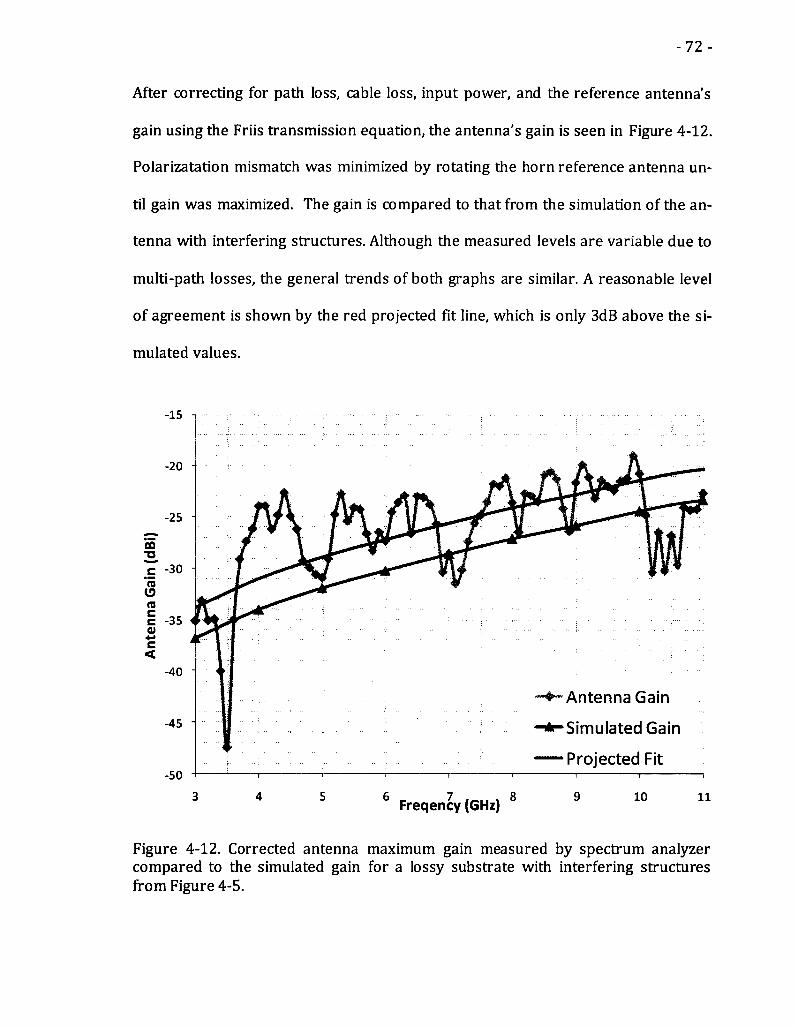
-72-
After correcting for path loss, cable loss, input power, and the reference antenna's
gain using the Friis transmission equation, the antenna's gain is seen in Figure 4-12.
Polarizatation mismatch was minimized by rotating the horn reference antenna un-
til gain was maximized. The gain is compared to that from the simulation of the an-
tenna with interfering structures. Although the measured levels are variable due to
multi-path losses, the general trends of both graphs are similar. A reasonable level
of agreement is shown by the red projected fit line, which is only 3dB above the si-
mulated values.
15
20
25
CQ
c -30re13re
e -35OJ
40
»-?"»Antenna Gain
45 Simulated Gain
Projected Fit-50 t '¦ 1 i 1 1 1 G
3 4 5 6 _ 7 .„„ . 8 9 10 11Freqency (GHz)
Figure 4-12. Corrected antenna maximum gain measured by spectrum analyzercompared to the simulated gain for a lossy substrate with interfering structuresfrom Figure 4-5.

-73-
This setup was then used again to estimate the radiation pattern of the antenna on
the IC. To accomplish this the horn antenna was rotated around the IC in the various
planes at a distance of 20 cm. Power readings were then taken at various positions
and the normalized shape of each pattern sketched in Figure 4-13. Note that the arcs
of the measurements are limited depending on the plane as the RF probe (located in
the +X direction) and the probing station present obstacles.
The measured normalized radiation patterns are significantly different from the si-
mulated patterns shown in Figure 4-4. Although the XY plane pattern for 3 GHz is
somewhat omnidirectional, the XY plane patterns for 7 and 10 GHz are directional.
Patterns in the XZ and YZ planes are also very directional, showing multiple lobes.
This result is somewhat expected as obstructions (the probe and probing station)
around the transmitter greatly affect the direction of the radiation of the antenna
due to reflections off the conducting surfaces. This exemplifies the need to use an
anechoic chamber for making radiation measurements; otherwise the possibility
that unaccounted environmental effects will disrupt an experiment is very likely.

-74-
12
9090 9CH90
80b)a
^X
12
15
9090
XY planeXZ planeYZ plane
19Figure 4-13. Measured and normalized 2D radiation patterns sketches at variousfrequencies: (a) 3.1 GHz, (b) 7 GHz, and (c) 10.6 GHz.
4.3.4.2 Antenna Measurements Using Network Analyzer
The second setup connected the antenna, via GSG probe, to port 1 of the network
analyzer, while port 2 of the network analyzer was connected to the horn antenna
reference. The horn antenna was then fixed a distance of 12 cm from the IC in the -X
direction similar to the measurement in Section 4.3.4.1. The signal was swept over 3
to 11 GHz at maximum power setting of 5 dBm and the full 2 port S-parameters

-75-
measured, shown in Figure 4-14. Before measurements were made with the net-
work analyzer, the system was calibrated using a calibration substrate. This allowed
the connecting cables and probes to be de-embedded from the measurements, giv-
ing more accurate results, although the horn reference antenna has to be manuallyde-embedded.
OQ -20
6 7 8Frequency (GHz)
10 11
Figure 4-14. Measured S-parameters using network analyzer connected directly tothe antenna.
The return loss (Sn) can be seen to be poor for an antenna, but significantly better
(lower) than that predicted by the simulations, seen in Figure 4-6. Although both
graphs show the return loss improving with frequency, the measured value has a
range of about 10 dB, where the simulated return loss had less than 1 dB change.

-76-
The return loss of port 2, S22, matches the expected behaviour of the horn reference
antenna, having a maximum value of approximately -9.4 dB, which is gives a VSWRof 2.
200
150
100
G 50?
p
<u
i -so
100
150 -*¦" Resistance
Reactance200 f.
10 118
Frequency (GHz)Figure 4-15. Input impedance of the antenna calculated from Sn
Calculated from Su, the input impedance is seen in Figure 4-15. The graph may look
somewhat strange, caused by the number of sample points being insufficient to dis-
play the high rate of change of the impedances. By qualitative interpolation it can beseen that the impedance is moving through many resonance points over the entire
spectrum. This is to some extent more easily seen in the Smith chart of Figure 4-16.Although plot lines are not shown on the Smith chart, what generally happens is the

-77-
plot rotates around the circle, slowly spiraling inwards, and crosses the real imped-
ance line many times. This occurs over most of the spectrum, except in the approx-
imate ranges: 5.6 to 6.2 GHz, 7.5 to 8.2 GHz, and 9.2 to 10 GHz, where the plot tends
to rotate in place.
? 9.6GHz3&7.8 GHz
«a
**M* 5.9 GHz'***11 GHz
/3 GHz
Simu atea? Measured
Figure 4-16. Smith chart graph of the simulated and measured Sn parameter of theantenna.

-78-
The measured/calculated input impedance varies significantly from the theoretical
simulation values. Although both rotate around the unit circle with an increase in
frequency, as seen in Figure 4-16, the simulated impedance does not cross the real
impedance line, staying inductive over the UWB spectrum. This is very different
compared to the measured data, which rotates several times around the Smith chart,
implying a highly resonant structure. This could in part be due to the probing pads
and the lines connecting the pads to the antenna input, which could not be de-
embedded with the network analyzer calibration routine.
After correcting for path loss, the reference antenna's gain, and assuming a polariza-
tion match, using a modified Friis transmission equation (the calibration of the net-
work analyzer accounted for cable losses and input power), the antenna's gain is
seen in Figure 4-17. The gain is compared to that from the simulation of the antenna
with interfering structures. Although the measured levels are variable due to multi-
path losses, the general trends of both graphs are very similar. There is a high de-
gree of agreement in the measured and simulated antenna gain.
The forward gain, S21, and the reverse gain, S12, from Figure 4-14 demonstrate the
reciprocity of the antenna system, both being almost equal. Similar to the measure-
ments in Section 4.3.4.1, the variance in the gain shows multi-path dependencies.
Both measurements show dips in the gain at approximately 3.5 GHz, 5 GHz, 7 GHz,
and 10.5 GHz.

-79-
-20 -,
-25
-30 H
5-35¦a
(O -40
-45
-50
-55
'S21
•Simulated
6 7 8Frequency (GHz)
10 11
Figure 4-17. Corrected antenna gain measured by network analyzer compared tothe simulated gain for a lossy substrate with interfering structures from Figure 4-5.
Measured phase response and group delay are shown in Figure 4-18. The phase is
approximately linear with an R2 value of 0.99 and having a slope giving an average
group delay of approximately 1.88 ns. This is a reasonable number considering thepath length of 12 cm. The range of the group delay over the entire UWB spectrum is
about 10 ns. The large group delay is mainly due to a sharp drop in the phase at
about 10.6 GHz, which corresponds to the sharp drop in gain as seen in Figure 4-17
and results in a significant increase in the group delay. Ignoring this point, the range
demonstrates a difference of about 4.5 ns, which is more reasonable, but still some-
what large compared to the absolute theoretical minimum of 0.8 ns [0.12 cm path

-80-
length). These results are consistent with the other data in indicating that there are
significant multi-path effects in the measurements.
r=-1.8826x+ 2.0675
S-IO
I
— Phase
-¦—Group Delay
MFrequency (GHz)
10 11
Figure 4-18. Measured phase response and group delay.
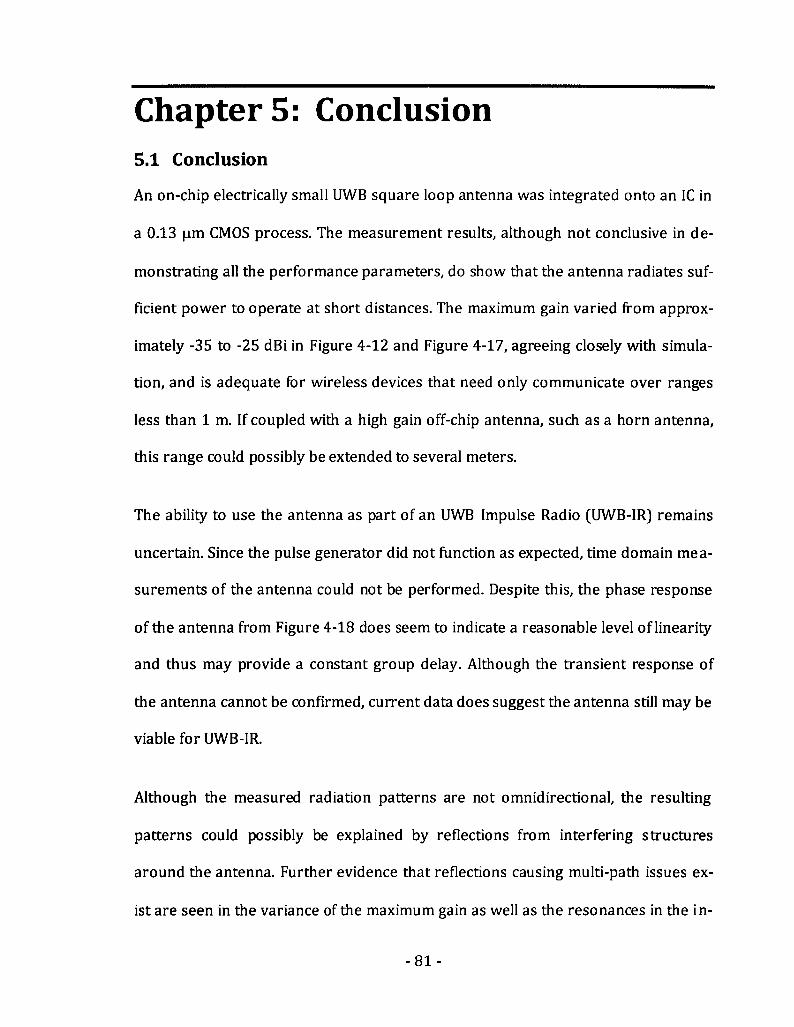
Chapter 5: Conclusion5.1 Conclusion
An on-chip electrically small UWB square loop antenna was integrated onto an IC in
a 0.13 µ?? CMOS process. The measurement results, although not conclusive in de-
monstrating all the performance parameters, do show that the antenna radiates suf-
ficient power to operate at short distances. The maximum gain varied from approx-
imately -35 to -25 dBi in Figure 4-12 and Figure 4-17, agreeing closely with simula-
tion, and is adequate for wireless devices that need only communicate over ranges
less than 1 m. If coupled with a high gain off-chip antenna, such as a horn antenna,
this range could possibly be extended to several meters.
The ability to use the antenna as part of an UWB Impulse Radio [UWB-IR) remains
uncertain. Since the pulse generator did not function as expected, time domain mea-
surements of the antenna could not be performed. Despite this, the phase response
of the antenna from Figure 4-18 does seem to indicate a reasonable level of linearity
and thus may provide a constant group delay. Although the transient response of
the antenna cannot be confirmed, current data does suggest the antenna still may be
viable for UWB-IR.
Although the measured radiation patterns are not omnidirectional, the resulting
patterns could possibly be explained by reflections from interfering structures
around the antenna. Further evidence that reflections causing multi-path issues ex-
ist are seen in the variance of the maximum gain as well as the resonances in the in-
-81-

-82-
put impedance. Although multi-path problems do not cause the antenna to cease to
function, they can render the antenna's radiation characteristics ambiguous. As
such, the antenna's radiation patterns cannot be confirmed or negated.
Even though the integrated UWB LNA and pulse generator circuits failed to operate
in a measureable way, important information and experience were garnered about
the design for test aspects of an on-chip antenna. Perhaps the most notable lesson:
the impractical i ty of driving an on-chip antenna from off-chip. The need to connect
the antenna from off-chip severely hampers attempts to characterize its perfor-
mance. This highlights the necessity to have a functioning signal source on-chip to
avoid extraneous components and equipment that may interfere with the antennas
operation. Another point of note is the need to better match the input impedance of
the antenna with the attached circuitry. Doing so over a wideband for electrically
small antennas is difficult and most likely would require co-design of the antenna
and circuitry as standard 50 O input/output impedances generally will not work.
5.2 Future Work
The main focus of continuing this research includes the creation of a working signal
source on-chip. By doing so, several issues and problems would be concurrently
solved. The design of the pulse generator, although functional for UWB, was made to
drive 50 Ü. It may not be possible to match such an impedance to an electrically
small antenna. Thus future work would include co-design of the antenna and pulse
generator, ensuring sufficient signal propagation between the two circuits.
-83-
As part of re-designing the pulse generator, the transient response of the antenna
could also be measured. In addition, with a fully integrated device, the IC could be
mounted on a PCB and used in an anechoic chamber. This would hopefully remove
any unwanted reflections and multi-path issues.
Re-design of the LNA may also be considered, although it is suggested that this cir-
cuit be removed from the IC. Having both the LNA and pulse generator on-chip over-
ly complicates the matching, requiring micro laser cutting to separate the circuits.
The LNA also requires probing to measure the received signal, thus not alleviating
the original issue. Of course, it may be advantageous to develop both the LNA and
pulse generator with the antenna as two separate ICs as operating the LNA and an-
tenna circuit can still provide some data. It may also be prudent to leave the LNA on-
chip, although disconnected, to gauge the effect of its presence on the antenna.
As an alternative to using the UWB pulse generator as the signal source, it may be
advantageous to use Voltage Controlled Oscillators (VCO). Although VCOs generally
are narrow band, there are examples that produce signals across the UWB spec-
trum. Although a VCO would not allow for transient response characterizations, rad-
iation patterns would be easily measured at the VCOs given frequency of operation.
Although radiation pattern measurements are not practical on a probing station, it
may still be worthwhile for determining the input impedance and return loss of the
antenna. For such measurements it is recommended that pad and transmission line

-84-
de-embedding structures are included in the design. With these structures, more
accurate input characteristics of the antenna could be determined.
Once the antenna is fully characterized, integration into a full transmitter and re-
ceiver would be the next step. This would also require the co-design of the antenna
and the new circuitry. Additionally, packaging considerations would need to be tak-
en into account as this design would approach a more commercial aspect. The an-
tenna would need to be re-characterized and the performance of the Tx/Rx meas-
ured. This could include using the transmitter and receiver as a pair or separately
with an off-chip antenna.

References
[I] G. Falciasecca and B. Valotti, "Guglielmo Marconi: the Pioneer of WirelessCommunications," in the 39th European Microwave Conference, Rome, 2009, pp.544-546.
[2] Nobel Foundation. (2010, Jun.) Nobelprize.org. [Online].http://nobelprize.org/nobel_prizes/physics/laureates/
[3] Federal Communications Commission, "Revision of Part 15 of the Commission'sRules Regarding Ultra-Wideband Transmission Systems," FCC, WashingtonD.C., First Report and Order 02-48, 2002.
[4] M. Z. Win, D. Dardari, A. F. Molisch, W. Wiesbeck, and J. Zhang, "History andApplications of UWB," Proceedings of the IEEE, vol. 97, no. 2, pp. 198-204, Feb.2009.
[5] Federal Communications Commision, "Title 47 of the Code of FederalRegulations," FCC Part 15, Radio Frequency Devices, Subpart F 15.500, 2009.
[6] Industry Canada, "Devices Using Ultra-Wideband (UWB) Technology,"Spectrum Management and Telecommunications Radio Standards SpecificationRSS-220, March 2009.
[7] W. Wiesbeck and G. Adamiuk, "Antennas for UWB-Systems," in Antennas, 2007.INICA '07. 2nd International ITG Conference on, Munich, March 2007, pp. 67-71.
[8] W. Wiesbeck, G. Adamiuk, and C. Sturm, "Basic Properties and Design Principlesof UWB Antennas," Proceedings ofthe IEEE, vol. 97, no. 2, pp. 372-385, Feb.2009.
[9] Zhi Ning Chen, "UWB Antennas: Design and Application," in 6th InternationalConference on Information, Communications & Signal Processing , Singapore,2007, pp. 1-5.
[10] J. S. Kilby, "The Integrated Circuit's Early History," Proceedings of the IEEE, vol.88, no. l.pp. 109-111, Jan. 2000.
[II] I. Young, "A History of the Continuously Innovative Analog Integrated Circuit,"
-85-

-86-
Solid-State Circuits Newsletter, IEEE, vol. 12, no. 4, pp. 52-57, Fall 2007.
[12] T. H. Lee, "The (Pre-) History of the Integrated Circuit: A Random Walk," Solid-State Circuits Newsletter, IEEE, vol. 12, no. 2, pp. 16-22, Spring 2007.
[13] K. K. O, et al., "On-Chip Antennas in Silicon ICs and Their Application," IEEETransactions on Electron Devices, vol. 52, no. 7, pp. 1312-1323, Jul. 2005.
[14] W. L. Stutzman and G. A. Thiele, Antenna Theory and Design, 1st ed. New York,USA: John Wiley & Sons, Inc., 1981.
[15] "IEEE Standard Definitions of Terms for Antennas.," IEEE Std 145-1993, vol.,no., pp.i, 1993. doi: 10.1109/IEEESTD.1993.119664.
[16] D. M. Pozar, Microwave Engineering, 2nd ed., C. Robey, Ed. New York, USA: JohnWiley & Sons, 1998.
[17] P. Popovski, H. Yomo, and R. Prasad, "Strategies For Adaptive FrequencyHopping in the Unlicensed Bands," IEEE Wireless Communications, vol. 13, no. 6,pp. 60-67, Dec. 2006.
[18] W. Y. Zou and Y. Wu, "COFDM: An Overview," IEEE Transactions onBroadcasting, vol. 41, no. 1, pp. 1-8, Mar. 1995.
[19] Hiroshi Iwai, "RF CMOS Technology," in Radio Science Conference, 2004.Proceedings. 2004 Asia-Pacific, 24 - 27 August 2004, pp. 296-298.
[20] Y. Cheng, "An Overview of Device Behavior and Modeling of CMOS Technologyfor RF IC Design," in The 11th IEEE International Symposium on Electron Devicesfor Microwave and Optoelectronic Applications, 2003. EDMO 2003., 17 - 18November 2003, pp. 109-114.
[21] Xiaoling Guo, Ran Li, and K. K. 0, "Design Guidlines for Reducing the Impact ofMetal Interference Structures on the Performance of On-chip Antennas," inAntennas and Propagation Society International Symposium, 2003. IEEE , 2003,pp. 606-609.
[22] F. Gutierrez, S. Agarwal, K. Parrish, and T. S. Rappaport, "On-Chip IntegratedAntenna Structures in CMOS for 60 GHzWPAN Systems," IEEEJournal onSelected Areas in Communications, vol. 27, no. 8, pp. 1367-1378, Oct 2009.
[23] M. Pons, F.Touati, and P. Senn, "Study of On-Chip Integrated Antennas UsingStandard Silicon Technology for Short Distance Communications," in TheEuropean Conference on Wireless Technology, 2005., Paris, 2005, pp. 253-256.

-87-
[24] A. Shamim, et al., "Silicon Differential Antenna/Inductor for Short RangeWireless Communication Applications," in Canadian Conference on Electricaland Computer Engineering, 2006. CCECE '06. , Ottawa, ON, 2006, pp. 94-97.
[25] L. Fragomeni, F. Zito, F. G. Della Corte, F. Aquilino, and M. Merenda, "CMOS FullyIntegrated 2.5GHz Active RFID Tag withOn-Chip Antenna," in MELECON 2010 -2010 15th IEEE Mediterranean EIectrotechnical Conference, Valletta, 2010, pp.922-926.
[26] J. J. H. Wang, "The Physical Foundation, Developmental History, and Ultra-wideband Performance of SMM (Spiral-Mode Microstrip) Antennas," in 2005IEEE Antennas and Propagation Society International Symposium, July 2005, pp.586-589vol3A.
[27] J. Liang, C. C. Chiau, X. Chen, and C. G. Parini, "Study of a Printed Circular DiscMonopole Antenna for UWB Systems," IEEE Transactions on Antennas andPropagation, vol. 53, no. 11, pp. 3500-3504, Nov. 2005.
[28] Y. Lu, Y. Huang, Y. C. Shen, and H. T. Chattha, "A Further Study of Planar UWBMonopole Antennas," in Antennas & Propagation Conference, 2009. LAPC 2009.,Loughborough , November 2009, pp. 353-356.
[29] Z. N. Chen, et al., "Planar Antennas," IEEE Microwave Magazine, vol. 7, no. 6, pp.63-73, Dec. 2006.
[30] H. G. Schantz, "Bottom Fed Planar Elliptical UWB Antennas," in 2003 IEEEConference on Ultra Wideband Systems and Technologies, November 2003, pp.219-223.
[31] M. Mao and C. Nguyen, "An Ultra-Wideband Uniplanar Antenna for UWBSystems," in 2008 International Radar Symposium, Wroclaw, 2008, pp. 1-3.
[32] L. Tianming, R. Yuping, and N. Zhongxia, "Analysis and Design of UWB VivaldiAntenna," in 2007 International Symposium on Microwave, Antenna,Propagation and EMC Technologies for Wireless Communications, Hangzhou,2007, pp. 579-581.
[33] V. Rumsey, "Frequency Independent Antennas," in IRE International ConventionRecord, 1957, pp. 114-118.
[34] G. Lu, P. Spasojevic, and L. Greenstein, "Antenna and Pulse Designs for MeetingUWB spectrum Density Requirements," in 2003 IEEE Conference on UltraWideband Systems and Technologies, 2003, pp. 162-166.

-88-
[35] J. A. Gonzalez, T. M. Babij, and K. Siwiak, "Diamond Dipole AntennaOptimization Using a Genetic Algorithm/Finite Difference Time Domain HybridTechnique.," in IEEE 10th Annual Wireless and Microwave TechnologyConference, 2009. WAMICON '09., Clearwater, FL, 2009, pp. 1-2.
[36] Y. Mushiake, "Self-Complementary Antennas," IEEE Antennas and PropagationMagazine, vol. 34, no. 6, pp. 23-29, Dec. 1992.
[37] H. A. Wheeler, "Fundamental Limitations of Small Antennas," Proceedings of theIRE, vol. 35, no. 12, pp. 1479-1484, Dec. 1947.
[38] L. J. Chu, "Physical Limitations of Omni-Directional Antennas," Journal ofApplied Physics, vol. 19, no. 12, pp. 1163-1175, Dec. 1948.
[39] A. K. Skrivervik, J. .-F. Zürcher, O. Staub, and J. R. Mosig, "PCS Antenna Design:The Challenge of Miniaturization," IEEE Antennas and Propagation Magazine,vol. 43, no. 4, pp. 12-27, Aug. 2001.
[40] S. E. Sussman-Fort and R. M. Rudish, "Non-Foster Impedance Matching ofElectrically-Small Antennas," IEEE Transactions on Antennas and Propagation,vol. 57, no. 8, pp. 2230-2241, Aug. 2009.
[41] J. S. McLean, "The Radiative Properties of Electrically-Small Antennas," in IEEEInternational Symposium on Electromagnetic Compatibility, 1994. SymposiumRecord. Compatibility in the Loop., Chicago, 1994, pp. 320-324.
[42] Y.-j. Kim, J.-k. Kim, J.-h. Kim, H.-y. Kim, and H.-m. Lee, "Negative PermeabilityMetamaterial Structure Based Electrically Small Loop Antenna," 10thInternational Conference on Advanced Communication Technology, 2008. ICACT2008., vol. 1, pp. 769-773, Feb. 2008.
[43] Z. N. Chen, T. S. P. See, and X. Qing, "Small Ground -independent Planar UWBAntenna," in IEEE Antennas and Propagation Society International Symposium2006, Albuquerque, NM, 2006, pp. 1635-1638.
[44] M. Klemm and G. Troster, "Integration of Electrically Small UWB Antennas forBody-Worn Sensor Applications," in Wideband and Multi-band Antennas andArrays, 2005. IEE (Ref. No. 2005/11059) , 2005, pp. 141-145.
[45] R. Saleem and A. K. Browne, "Electrically Small Band-Notch Reflected InverseParabolic Step Sequence Ultra Wideband Antenna," in 2010 Proceedings of theFourth European Conference on Antennas and Propagation (EuCAP), Barcelona,Spain , 2010, pp. 1-3.
-89-
[46] M. Ikebe, et al, "A 3.1-10.6 GHz RF CMOS Circuits Monolithically Integratedwith Dipole Antenna," in 16th IEEE International Conference on Electronics,Circuits, and Systems, 2009. ICECS 2009. , Yasmine Hammamet, December 2009,pp. 17-20.
[47] K. Takahagi, M. Ohno, M. Ikebe, and E. Sano, "Ultra-Wideband Silicon On-ChipAntenna with Artificial Dielectric Layer," in International Symposium onIntelligent Signal Processing and Communication Systems, 2009. ISPACS 2009.,Kanazawa, 2009, pp. 81-84.
[48] K. T. Ansari and C. Plett, "A Low Power Ultra-Wideband CMOS LNA for 3.1-10.6-GHz Wireless Receivers," in Proceedings of2010 IEEE International Symposiumon Circuits and Systems (ISCASJ, Paris, France, 2010, pp. 209-212.
[49] O. Salehi-Abari and C. Plett, "A Differential 5th Derivative Gaussian PulseGenerator for UWB Transceivers," in Proceedings of2010 IEEE InternationalSymposium on Circuits and Systems (ISCASJ, Paris, France, 2010, pp. 1089-1092.
[50] Ansys Inc. (2010) Ansoft - HFSS. [Online].http://www.ansoft.com/products/hf/hfss/