a true single-phase energy-recovery multiplier - very large scale
TRANSCRIPT

194 IEEE TRANSACTIONS ON VERY LARGE SCALE INTEGRATION (VLSI) SYSTEMS, VOL. 11, NO. 2, APRIL 2003
A True Single-Phase Energy-Recovery MultiplierSuhwan Kim, Member, IEEE, Conrad H. Ziesler, Student Member, IEEE, and
Marios C. Papaefthymiou, Senior Member, IEEE
Abstract—In this paper, we present the design and experimentalevaluation of an 8-bit energy-recovery multiplier with built-inself-test logic and an internal single-phase sinusoidal power-clockgenerator. Both the multiplier and the built-in self-test have beendesigned in SCAL-D, a true single-phase adiabatic logic family.Fabricated in a 0.5- m standard n-well CMOS process, the chiphas an active area of 0.47 mm2. Correct chip operation has beenverified for clock rates up to 140 MHz. Moreover, chip dissipationmeasurements correlate well with HSPICE simulation results. Fora selection of biasing conditions that yield correct operation at 140MHz, total measured average dissipation for the multiplier andthe power-clock generator is 250 pJ per operation.
Index Terms—Adiabatic design, arithmetic circuits, chargerecovery, dynamic circuits, LC tank circuits, low-energy circuits,low-power circuits, very large scale integration (VLSI) design.
I. INTRODUCTION
ENERGY recovering (a.k.a. adiabatic) logic presents apromising alternative to conventional CMOS for the real-
ization of low-energy electronics. In adiabatic circuits, energydissipation is kept low by maintaining low voltage drops acrossconducting devices. Moreover, undissipated energy relatedto charges stored in parasitic capacitors is recycled throughan inductor or network of switched capacitors [1]–[3]. Thus,adiabatic circuitry can potentially achieve sub- energydissipation per cycle, where is the total switched capacitanceand is the peak supply voltage.
A plethora of adiabatic circuit topologies has been proposedover the past decade. Most of these circuits have relied on mul-tiple-phase power-clocks to steer currents and recycle charges[4]–[9]. Thus, they are not attractive for high-speed design, dueto their relatively complex control requirements, further exac-erbated by the data-dependent fluctuations of the power-clockload [10]. In contrast to multiphase circuits, true single-phaseadiabatic circuits rely on just one phase of a power-clock wave-form for power and synchronization [11]–[13]. Thanks to theirsimple clocking requirements, single-phase circuits enjoy min-imal control overheads and are thus capable of operating at highspeeds, while achieving high-energy efficiency.
Manuscript received November 13, 2001; revised August 3, 2002. Thiswork was supported in part by the Army Research Office under GrantDAAD19-99-1-0304 and by an AASERT Grant DAAG55-97-1-0250.
S. Kim was with the Advanced Computer Architecture Laboratory, Depart-ment of Electrical Engineering and Computer Science, University of Michigan,Ann Arbor, MI 48109 USA. He is now with Low Power Circuits and Tech-nology, IBM Thomas J. Watson Research Center, Yorktown Heights, NY 10598USA (e-mail: [email protected]).
C. H. Ziesler and M. C. Papaefthymiou are with the Advanced ComputerArchitecture Laboratory, Department of Electrical Engineering and ComputerScience, University of Michigan, Ann Arbor, MI 48109 USA (e-mail:[email protected]; [email protected]).
Digital Object Identifier 10.1109/TVLSI.2003.810795
We recently embarked on the design of an 8-bit adiabaticmultiplier using SCAL-D, a source-coupled adiabatic logicfamily that operates with a single-phase power-clock [14],[15]. In view of previous adiabatic multiplier designs that usedmultiple power-clocks and achieved rather modest operatingspeeds [16]–[18], the main objective of our research projectwas to demonstrate the feasibility of designing adiabaticcircuitry that functions correctly and efficiently at relativelyhigh power-clock frequencies (100 MHz and above). To enableat-speed testing and the measurement of power dissipationwithout the complications and interference caused by chipI/O, our multiplier included built-in self-test (BIST) circuitrythat was also designed in SCAL-D. Moreover, to decouple thetesting of the multiplier core from the power-clock generationcircuitry, our chip was designed so that the the multiplier couldbe driven using either an external or an internal power-clockgenerator.
Our multiplier chip was fabricated in a 0.5m standardn-well CMOS process through MOSIS. The correct operationof our chip was validated in the lab with a 3 V power supplyfor clock rates up to 140 MHz. The power supply level was notlimited by SCAL-D. It was primarily dictated by the peripheralcircuits, including adiabatic-to-digital converters and outputpad drivers, and our experimental setup, including the test boardand oscilloscope probes. In general, the measured trend ofdissipation correlated well with HSPICE simulations for iden-tical biasing conditions. For example, under a set of conditionsthat ensured correct operation at 140 MHz, the total measureddissipation of our multiplier, including its internal power-clockgenerator, was 250 pJ per operation, approximately 20% lowerthan HSPICE-based results.
This paper describes the design and experimental evaluationof our adiabatic multiplier. We discuss in detail the circuit,layout, and power-clock distribution issues of our adiabaticchip and internal power-clock generator. We also discuss thedesign and verification methodologies developed to facilitatethe use of SCAL-D in conjunction with the layout tool MAGIC,the circuit simulator HSPICE, and structural Verilog-HDLdescriptions.
In addition to power measurements, our paper includes a sim-ulation-based comparison of our multiplier with several staticCMOS multipliers synthesized for low power. In HSPICE simu-lations with post-layout extracted parasitics, our multiplier func-tions correctly at clock rates exceeding 200 MHz, while dissi-pating up to four times less energy than its CMOS counterparts.Both our experimental measurements and our simulation resultssuggest that SCAL-D is a practical circuit topology for high-per-formance, low-energy adiabatic systems.
The remainder of this paper has seven sections. In Section II,we describe the structure and operation of SCAL-D. In Sec-
1063-8210/03$17.00 © 2003 IEEE

KIM et al.: A TRUE SINGLE-PHASE ENERGY-RECOVERY MULTIPLIER 195
(a) (b)
Fig. 1. (a) A pMOS and (b) an nMOS buffer in SCAL-D.
tion III, we present simple analytic loss models for SCAL-D.The design and implementation of the 8-bit SCAL-D multiplieralong with its BIST logic and internal power-clock generator aredescribed in Section IV. Section V provides an overview of ourdesign methodologies we developed for SCAL-D. Section VIpresents a comparison of our adiabatic multiplier with compa-rable static CMOS designs. Section VII provides results fromthe testing and experimental evaluation of our fabricated chip.Our contributions are summarized in Section VIII.
II. SOURCE-COUPLED ADIABATIC LOGIC
This section describes SCAL-D, our source-coupled adi-abatic logic with diode-connected transistors. The structureand operation of SCAL-D are similar to those of SCAL[12]. SCAL-D retains all the positive features of SCAL [13],including correct operation with single-phase power-clock.Furthermore, it achieves energy efficient operation acrossa broad range of operating frequencies by using a pair ofcross-coupled transistors and an individually tunable currentsource at each gate.
A. SCAL-D Gates
The basic structure of a SCAL-D pMOS gate is shown inFig. 1(a). This pMOS buffer comprises a pair of cross-coupledtransistors ( and ), a pair of diode-connected transis-tors ( and ), a pair of current control switches ( and
), two evaluation trees ( and ), and a current source( and ) biased by a constant voltageBP and a sinusoidalpower-clock PC. A constant supply voltageDD is required toimpart an initial charge to one of the output nodes (and )through the evaluation tree. The quantity of charge transferredfrom dd is controlled by the ratio of the cascoded tran-sistors of the current source ( and ) and the bias voltageBP.The basic structure of a SCAL-D nMOS gate is shown in
Fig. 1(b). It has the same structure as the pMOS gate, but itscurrent source is tied toSS. The biasing voltageBN may differfrom BP.
B. SCAL-D Operation
In this section, we highlight the operation of SCAL-D pMOSgates and points out its differences from SCAL. The operationof SCAL-D nMOS gates is similar to that of their pMOS coun-terparts.
Each SCAL-D pMOS gate goes through anevaluateand adischargephase. Duringdischarge, the energy stored in the node
or is recovered through the pair of cross-coupled transis-tors ( or ) and the pair of diode-connected transistors( and ). In this phase, PC starts fromhigh and rampsdown towardlow, pulling both and down toward the pre-discharge voltage. This state change tracks the power-clock and,thus, recovers charge from the output nodes. It is not fully adi-abatic, however, since some of the charge is recovered througha device with a constant voltage drop.
A new output is computed duringevaluate. In the beginningof this phase, a dissipative current is directed by the evaluationtree, creating a small voltage imbalance between the cross-cou-pled transistors. Even though all the gates of the same type havethe same biasing voltage, the amount of this current is individu-ally controlled by the ratios of the current source transis-tors. Thus, the dissipation of each gate can be minimized underany output load or operating frequency. After the nonadiabaticevaluation, the current source is turned off, and the load is drivenadiabatically by the sense amplifier with the rising ofPC.
The operation of SCAL-D is similar to that of SCAL. Themain difference between the operation of the two gates is inthe method that output loads are discharged and in the flexi-bility provided for tuning the current source. In SCAL-D, thedischarge time is shortened by adding the diode-connected tran-sistors to provide additional current. Moreover, the magnitudeof the current in the beginning ofevaluatecan be controlledby adjusting the ratios of and in each gate andby tuning the dc biasing voltageBP that is shared by all pMOSgates. For a given operating frequency, the duration of the nona-diabatic stage duringevaluatecan be controlled by adjusting thebiasing voltage BP.
The operation of the SCAL-D nMOS gate is similar to thatof the pMOS gate. Instead ofprecharge, the first phase in the

196 IEEE TRANSACTIONS ON VERY LARGE SCALE INTEGRATION (VLSI) SYSTEMS, VOL. 11, NO. 2, APRIL 2003
Fig. 2. Four-stage PNPN cascaded pipeline in SCAL-D.
operation of the nMOS gate ischarge. The second phase is stillevaluate.
C. SCAL-D Cascades
To build SCAL-D cascades, pMOS, and nMOS gates arechained alternately. The only signal required to control aSCAL-D cascade is a single phase of the power-clockPC.The speed and energy efficiency of a SCAL-D cascade can betuned by sizing the current source in each gate and choosingthe two dc biasing voltages. Since individual gates can be tunedindependently, efficient operation can be achieved for a broadrange of operating frequencies.
A four-stage PNPN cascade structure of SCAL-D buffers isshown in Fig. 2. This figure also shows the power clockPCand the two dc biasing voltagesBP and BN that are requiredto control the SCAL-D cascade. At any time during the opera-tion of the circuit, either all pMOS gates evaluate and all nMOSgates charge, or all pMOS gates discharge and all nMOS gatesevaluate. The brief time interval between evaluate/discharge orevaluate/charge during which the outputs of a gate are stable iscalled theholdphase in that gate’s operation. While the currentswitches in the odd stages are off, their outputs are stable. At thesame time, the function blocks of the even stages are connectedto DD (or SS) through the current sources and can safely eval-uate their outputs. After half a cycle, while the current switchesof the even stages are off, the inputs of the odd stages are stable,and their function blocks are connected toSS (or DD) throughtheir current sources.
III. POWER-LOSSMODELS
In this section, we present analytic power-loss modelsfor the power-clock distribution wire, the diode-connectedtransistors, the cross-coupled transistors, and the nonadiabaticfunction evaluation tree in SCAL-D. Each SCAL-D nMOSor pMOS gate precharges or discharges its output nodes,evaluates its function evaluation tree, and drives its outputswithin radians, with the power-clock source given byPC A , where A dd and . For
the power-loss models of a SCAL-D nMOS gate, we assumethat the precharge of output nodes through diode-connectedtransistors occurs between and , the nonadiabaticcharge transfer through the current source occurs between
and , and the cross-coupled transistors boost the voltagedifference between the two output nodes between and
. The SCAL-D pMOS gates operateradians out of phasewith the nMOS gates.
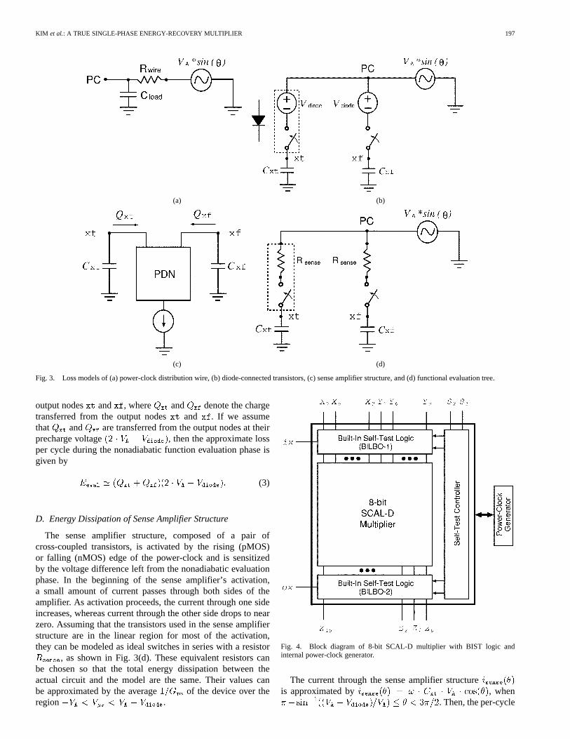
A. Energy Dissipation of Power-Clock Distribution Wire
When modeling a power-clock distribution wire, as shownin Fig. 3(a), the total resistance is lumped into a single resistorwire, and the global capacitance is combined into a single ca-
pacitor load. The current through a power-clock distributionwire wire is defined aswire load A ,when . Then, the energy consumption percycle due to this wire wire is given by
wire wire load A(1)
B. Energy Dissipation of Diode-Connected Transistors
The diode-connected transistors can be replaced by idealdiodes, considered to be switches in series with a diode forwardvoltage diode as shown in Fig. 3(b). The output node capaci-tances xt and xf are precharged through the forward biaseddiode and represent the sum of all diffusion, junction, wiring,and fanout capacitances connected to the output nodesand
, respectively.If we assume that xt A diode and xf A,
then the diode currentsxt and xf are defined asxt and xf xf A , when
A diode A . Then, the energyconsumption per cycle of the diode-connected transistors,diode, is given by the expression
diode A diode diode xt (2)
C. Energy Dissipation of Non-Adiabatic Function EvaluationTree
Non-adiabatic operation occurs in the beginning of eachgate’s function evaluation phase. During this phase, chargestored in the output nodes and is discharged through thetrue and falsebranches of the gate’s function evaluation tree,as shown in Fig. 3(c). The result of this operation is to create avoltage difference xt xt xf xf between the two
KIM et al.: A TRUE SINGLE-PHASE ENERGY-RECOVERY MULTIPLIER 197
(a) (b)
(c) (d)
Fig. 3. Loss models of (a) power-clock distribution wire, (b) diode-connected transistors, (c) sense amplifier structure, and (d) functional evaluation tree.
output nodes and , where xt and xf denote the chargetransferred from the output nodes and . If we assumethat xt and xf are transferred from the output nodes at theirprecharge voltage A diode , then the approximate lossper cycle during the nonadiabatic function evaluation phase isgiven by
eval xt xf A diode (3)
D. Energy Dissipation of Sense Amplifier Structure
The sense amplifier structure, composed of a pair ofcross-coupled transistors, is activated by the rising (pMOS)or falling (nMOS) edge of the power-clock and is sensitizedby the voltage difference left from the nonadiabatic evaluationphase. In the beginning of the sense amplifier’s activation,a small amount of current passes through both sides of theamplifier. As activation proceeds, the current through one sideincreases, whereas current through the other side drops to nearzero. Assuming that the transistors used in the sense amplifierstructure are in the linear region for most of the activation,they can be modeled as ideal switches in series with a resistorsense, as shown in Fig. 3(d). These equivalent resistors can
be chosen so that the total energy dissipation between theactual circuit and the model are the same. Their values canbe approximated by the average of the device over theregion A A diode.
Fig. 4. Block diagram of 8-bit SCAL-D multiplier with BIST logic andinternal power-clock generator.
The current through the sense amplifier structuresense
is approximated bysense xt A , whenA diode A . Then, the per-cycle

198 IEEE TRANSACTIONS ON VERY LARGE SCALE INTEGRATION (VLSI) SYSTEMS, VOL. 11, NO. 2, APRIL 2003
Fig. 5. Schematic of a parallel multiplier cell containing a 1-bit full-adder and a buffer cell in SCAL-D.
energy consumption of the sense amplifier structuresense isapproximated by
sense sense A xt(4)
E. Total Energy Dissipation
The total energy consumption per cycle is given by the sumof (1) through (4) for radians of the power-clock. The loss ofthe power-clock distribution wire and sense amplifier structureis proportional to its operating frequency. The loss of diode-connected transistors is proportional todiode.
Low energy consumption is achieved by careful transistorsizing with the aim to balance the various dissipation compo-nents while providing for correct functionality at an efficientoperating condition (frequency, supply voltage, bias voltage).The primary tradeoff is between the energy dissipated throughthe nonadiabatic function evaluation tree and the energy dissi-pated in the sense amplifier structure. This tradeoff is affectedboth by transistor sizing and choice of bias voltages.
IV. M ULTIPLIER, BIST LOGIC, AND POWER-CLOCK
GENERATOR
To demonstrate the practicality of SCAL-D, we used it to de-sign and fabricate an 8-bit multiplier with BIST logic in a 0.5
m standard n-well CMOS process. The design was fabricatedby TSMC through MOSIS. In this Section, we present the cir-cuit, logic, and structure of our 8-bit SCAL-D multiplier, BISTlogic, and internal single-phase power-clock generator.
Typically, multiplication involves the evaluation and accu-mulation of shifted partial products. These operations can beperformed in several different ways. In general, the choice ofa particular multiplication scheme is based on factors suchas speed, throughput, numerical accuracy, area, and power[19]–[24]. Since each SCAL-D gate combines both logic and
Fig. 6. Layout of a parallel multiplier cell containing a 1-bit full-adder and abuffer cell in SCAL-D.
state holding functions, we chose to implement a fully pipelinedcarry-save multiplier architecture. As shown in Fig. 4, oursystem consists of an 8-bit unsigned multiplier, BIST logic, andan internal single-phase power-clock generator. The multiplierand BIST logic are implemented entirely in SCAL-D. Thevoltages dd, ss, and PC are supplied to each SCAL-D gate.
A. Multiplier and BIST Logic
The multiplier is constructed from a set of basic cells, themost critical and complicated of which is the 1-bit full addercell. The schematic and physical layout of this 1-bit full addercell in SCAL-D, shown in Figs. 5 and 6, contain the equiva-lent of 3-bits of state elements along with the full adder logic.Our SCAL-D implementation uses 85 transistors. An equivalentstatic CMOS implementation would require 100 transistors, in-cluding 28 transistors for a 1-bit full adder logic and 72 transis-tors for 3 flip-flops [25].
Our BIST logic is based on Koenemann’s built-in logic blockobserver (BILBO) [26], which uses a linear feedback shift reg-ister (LFSR) to both generate a pseudorandom pattern for the

KIM et al.: A TRUE SINGLE-PHASE ENERGY-RECOVERY MULTIPLIER 199
Fig. 7. TYPE-2 implementation of 16-stage BILBO in SCAL-D.
Fig. 8. Full-custom layout of 8-bit multiplier with associated BIST logic inSCAL-D.
circuit under test and perform signature analysis [25], [27]. Weimplemented our BILBO entirely in SCAL-D, thus enablingfull-speed testing without any I/O synchronization issues. Fig. 7shows the block diagram of our SCAL-D BILBO. To generatethe maximum-length sequences, a primitive polynomial
was used to build a LFSR. In normal op-eration mode, the BILBO acts as a set of latches. In the self-testmode, however, the BILBO is converted into LFSRs. Mode se-lection is controlled by the signals and . Each circuit undertest has pseudorandom patterns applied to its inputs, and its out-puts are compressed to form a signature. Specifically, BILBO-1and BILBO-2 in Fig. 4 are configured as a pseudorandom pat-tern generator and a multiple input signature register, respec-tively. The output sequences of BILBO-1 and BILBO-2and
must be observed to infer the correct operation of the entiremultiplier.
The full-custom layout of the 8-bit multiplier and its asso-ciated BIST logic in Fig. 8 was designed and implemented inSCAL-D. It contains 11 854 transistors, of which 2806 transis-tors (about 24%) are used in the BIST logic, and the remaining9048 transistors (about 76%) in the multiplier. The total area ofthe design is approximately 0.710 mm( 0.829 mm 0.857mm), including the multiplier core of 0.470 mm( 0.781 mm
0.607 mm), in a 0.5-m standard n-well CMOS process. The
Fig. 9. Internal single-phase power-clock generator and off-chip connections.
Fig. 10. Balanced pulse-alternating asynchronous state machine used inpower-clock generator.
capacitance of our power-clock distribution wires contributes57% of the total capacitance loading of the power-clock node.The remaining capacitance of power clock is distributed be-tween the signal interconnect and the transistor loads, both ofwhich were drawn to be balanced with respect to the dual rails.These factors contribute to an effective power-clock capacitancethat is nearly time-invariant.
For the evaluation tree of each gate, minimum-size transistorswere used with ratio equal to . To enhance the energyefficiency of SCAL-D, the ratio of each current sourceand cross-coupled transistor pair was selected according to thetarget operating frequency, the capacitive load at the output ofthe gate, and the power-clock supply voltage level.PC, DD, andSS were routed using wide wires primarily on metal layers 2
and 3. BP and BN were routed primarily on polysilicon underlocal DD and SS interconnect. This approach minimizes dif-ferential mode noise between the bias and supply nodes whileconsuming very few routing resources.
B. Power-Clock Generator
An internal single-phase sinusoidal power-clock generatorwas designed using the topology shown in Fig. 9. It consistsof an resonant system, two power switches (pMOS andnMOS), an asynchronous state machine, and a three-elementdifferential logic ring oscillator. The ring oscillator is tuned overa small range of frequency and duty cycles by two bias volt-ages. The output of the ring oscillator is a train of pulses whichfeeds the asynchronous state machine. The state machine, asshown in the schematic of Fig. 10, simply alternates the pulses

200 IEEE TRANSACTIONS ON VERY LARGE SCALE INTEGRATION (VLSI) SYSTEMS, VOL. 11, NO. 2, APRIL 2003
Fig. 11. Full-custom layout for the power-clock generator, including guardrings and driver transistors.
to each of its two outputs while preserving the pulse width.The two outputs are then buffered and drive the gates of thepMOS and nMOS switches. Fig. 11 shows the final layout forthe power-clock generator. Not shown is a large bypass capac-itor which is four times the size of the power-clock generator.
The system is composed of an off-chip/bondwireinductor coupled with the on-chip adiabatic load capacitance.This simple harmonic resonant system is pumped using azero-voltage switching scheme. The pMOS switch is turned onat the peak of the sinusoid, where the voltage difference betweendd and PC is nearly zero. The nMOS switch is turned on at
the negative peak of the sinusoid, where the voltage differencebetween PC and ss is nearly zero. This scheme can minimizeboth conduction and switching losses [28]. Specifically, con-duction losses are minimized, because each device conductsa current at mostswitch loss half-cycle resonant .Switching losses are minimized at the same time, since theenergy stored in the parasitic source-to-drain capacitance isnearly zero when the voltage difference betweendd and PC
or between PC and ss is zero.The overall losses of the power-clock generator can be classi-
fied into two components: fixed, which is independent of loadsize, and variable, which scales with the load.fixed includesthe losses of the asynchronous state machine and ring oscillator,and amounts to roughly 1–2 mW at 3 V, depending on ring os-cillator tuning. variable includes all losses attributable to tran-sistors whose sizes need to be scaled with the load, includingthe power FETs and its drivers. Because our multiplier is a rela-tively small design, these transistor sizes are not very large, andso we observe variable to be nearly the same asfixed (i.e.,in the range of a few mW, depending on frequency and loaddissipation). Thus, as we consider larger designs, we expect therelative overhead of the power-clock generator to decrease, asthe overall dissipation tracksvariable, which itself scales lin-early with load dissipation, and the constant overhead offixed
is amortized over a larger total dissipation.In our design, we chose to slightly oversize switchesandso as to make the clock generator capable of driving the adi-
abatic multiplier even if the dissipation of the multiplier washigher than expected. As the optimum condition for sizing,
, and their associated driver buffers is rather broad, it is rela-tively easy to choose appropriate sizes. The sizes are, of course,very dependent on the total load dissipation, as this determinesthe peak current constraints placed onand .
Another important aspect of our power-clock generator isthe effect of design size scaling on the losses attributed tobondwire and package parasitics. From the familiar relation
, note that the frequency is inversely propor-tional to and . Thus, for a design of size that uses teninductor wires in parallel (thus reducing parasitic resistance),we expect the same relative fraction of parasitic losses as wewould for a design of size that uses one inductor.
V. DESIGN METHODOLOGIES
This section describes the design methodologies developedfor our adiabatic circuits. Our design methodologies differ fromconventional design practices for several reasons. First, eachgate is inherently a combinational circuit plus a state element.Therefore, each pipeline stage includes only one level of logic.Second, since every signal is in phase with the power-clocksignal, timing analysis is replaced with analog signal integrityanalysis. Phase delays are thus interpreted as a reduction insignal amplitude. Third, as each gate often only needs minimumsized evaluation transistors, fanout load is a function of the logicbeing implemented and wire length. Consequently, transistorsizing for each gate is independent of other gates to a certainextent.
In static CMOS we can define delays based on rising andfalling edges of signals and sum up the worst case delay througha network of gates. In SCAL-D logic, however, every signalin the system shares the same fundamental sinusoid as powerclock. A “slow” or “weak” gate results in lower amplitude sig-nals than a “fast gate.” Furthermore, a “long” wire results inboth a lower amplitude and a slightly out-of-phase output signal.Since our adiabatic gates have a discrete period in which theysample their inputs, we can convert any phase delay into anequivalent amplitude reduction, as seen by the inputs of the nextstage. Thus, the timing analysis problem is transformed in theadiabatic domain into a signal integrity checking problem. Ourfunctional verification tool also analyzes all the internal adi-abatic signals to determine if they meet our specification forsignal integrity. The maximum clock frequency our design iscapable of operating at is defined as the maximum frequency atwhich every signal meets our signal integrity check.
As the design progressed into layout, HSPICE simulationswere run on the adiabatic subcircuits. The trace data from thesesimulations were post-processed by a custom tool which veri-fied that each gate’s input and output voltage waveforms corre-sponded to correct logical evaluation. The output of this tool wasa list of failing gates along with layout coordinates, which en-abled us to rapidly diagnose and correct failures resulting fromsubtle analog considerations. This tool also enabled us to applyseveral heuristic transistor sizing rules, based on extracted par-asitic information from the layout.
VI. SIMULATION RESULTS
Although other researchers have designed multipliers to testvarious novel CMOS circuit families, (e.g., the serial-parallellocally-clocked dynamic-logic multiplier in [19] and thelow-power multiplier with pulse-triggered flip-flops in [20]),

KIM et al.: A TRUE SINGLE-PHASE ENERGY-RECOVERY MULTIPLIER 201
Fig. 12. Relative energy consumption per cycle versus operating frequencies for 8-bit multipliers with associated BIST logic.
any performance comparison of our design with published oneswould necessarily involve extrapolating the published data tocompensate for differences in process technology, bit-widths,multiplier architectures, target throughput, and experimentalmethodology. Thus, to perform a well-defined comparison,we implemented fully-static CMOS versions of our adiabaticmultiplier, synthesized for low power using best-practicedesign automation tools. In this section, we present a simula-tions-based comparative evaluation of our adiabatic multiplierand pipelined counterparts of our design in static CMOS.
Three pipelined CMOS multipliers with latency 2, 4, and 8,respectively, were synthesized using a library of standard cellsfor the same 0.5 m process in which our multiplier was fabri-cated. Flip-flops were used as the state elements. Layouts weregenerated using the Epoch design automation tool with stan-dard cells optimized for power dissipation. The static CMOSdesigns used 5,146, 6,518, and 9,926 transistors for the two-,four-, and eight-stage pipelines, respectively. Their area was ap-proximately 0.20 mm, 0.25 mm, and 0.36 mm, respectively.
Fig. 12 gives the relative energy consumption per cycle ofthe multipliers and associated BIST logic when operating at 50MHz, 100 MHz, and 200 MHz. For each operating frequency,the energy dissipation of each multiplier was obtained using thelowest supply voltage that ensures its correct operation at thatfrequency. Minimum supply voltage values are given next to thecorresponding data points. The simulations accounted for thedissipation of the gates and internal clock lines and assumed alossless external clock generator.
The energy consumption of our adiabatic multiplier scalesalmost linearly with supply voltage and remains pretty muchconstant with respect to frequency. Based on our energy lossmodels, diode and evaluation tree dissipation dominate senseamplifier dissipation in the operating regime of our simulations.Even though our adiabatic multiplier was designed conserva-tively at the expense of some energy consumption or perfor-mance optimizations, our results show that it is more energy
efficient than its pipelined static CMOS counterparts across theentire frequency range of our simulations. At 50 MHz, it is 1.4to 1.8 times more efficient than the pipelined static CMOS de-signs. At 100 MHz, it is 2.1 to 3.2 times more efficient than thethree static CMOS designs. At 200 MHz, our SCAL-D designis about four times more efficient than the eight-stage pipelinedstatic CMOS. The two- and four-stage static CMOS multipliersdo not function correctly at that frequency. In the pipelined staticCMOS multipliers, flip-flops are used to reduce critical pathsand decrease the required supply voltage. However, the resultingincrease in the circuit’s effective capacitance and clock distribu-tion network limits energy savings. Thus, SCAL-D presents apromising approach to further reducing the dissipation of staticCMOS designs that have reached their voltage scaling limits.
VII. EXPERIMENTAL RESULTS
In this section, we present the results of our experimentalmeasurements from the fabricated chip. To increase the testa-bility of our design, two identical 8-bit SCAL-D multiplierswere placed on each chip. One was powered by an externalsignal generator, while the other was wired directly to the in-ternal power-clock generator. We validated correct operation ofeach of the components of the chip independently. The multi-plier was validated up to a frequency of 130 MHz using an ex-ternal power-clock generator, limited by the slew rate of the padsand coupling between the pins. The power-clock generator wasalso validated to function correctly at 140 MHz.
The energy dissipation of the multiplier while driven by anexternal source of power-clock was measured for frequenciesbetween 40–130 MHz. These measurements were within 20%of HSPICE simulations for the 40–100-Hz range. The combinedmultiplier and clock generator dissipation was measured at afrequency of 140 MHz, and was within 20% of the HSPICEsimulation.

202 IEEE TRANSACTIONS ON VERY LARGE SCALE INTEGRATION (VLSI) SYSTEMS, VOL. 11, NO. 2, APRIL 2003
Fig. 13. Microphotograph of the chip.
Fig. 14. Simplified floorplan of the chip shown in Fig. 13
A die photo and simplified floorplan of our 8-bit SCAL-Dmultipliers and internal power-clock generator are shownin Figs. 13 and 14, respectively. The chip was fabricated
in a 0.5- m single-poly triple-metal n-well CMOS processthrough MOSIS. The chip includes the two 8-bit SCAL-Dmultipliers with BILBO, an internal power-clock generator,

KIM et al.: A TRUE SINGLE-PHASE ENERGY-RECOVERY MULTIPLIER 203
Fig. 15. Experimental setup for testing and measuring the power dissipationof the 8-bit SCAL-D multiplier chip.
adiabatic-to-digital converters (denoted by A/D), and I/O pads.The entire chip area is 4.83 mm(=2.60 mm 1.84 mm).
The A/D converters consist of cross-coupled inverters withtwo pull-down transistors connected to the adiabatic inputs. Thecross-coupled inverters restore the signal to full swing. The A/Dconversion circuitry was designed to enable testing using con-ventional digital signaling conventions. It is powered from theI/O power supply to enable full-swing drive of the I/O pads, re-gardless of any supply voltage differences between I/O and themultiplier under test. Thus, our power dissipation measurementsdo not include the A/D converter dissipation.
Fig. 15 shows our setup for test and measurement of the chip.On the right we have two dc power supplies and a TektronixTDS754D 4-channel 4 10 samples/s digitizing oscilloscope,configured with two 1-Hz high-impedance active probes, a 1-Hzdifferential active probe, and one passive probe. On the left wehave a HP 8647A synthesized signal generator, and a digitalmultimeter. Not shown is a 2-RF amplifier and power supplyused for boosting the amplitude from the signal generator. Ourdevice under test is inserted into a socket on the test board seenin the center of the picture. We verified the functional correct-ness of our SCAL-D multiplier and measured its power con-sumption, including its BIST logic, for up to 50s, the limit ofthe digital oscilloscope memory. All of the measurements wereperformed with the supply voltage fixed at 3 V, as dictated bythe peripheral circuits, including adiabatic-to-digital convertersand pad drivers.
The correct operation of the adiabatic multiplier and its BISTlogic was verified up to 130 MHz, using an external power-clockgenerator. Figs. 16 and 17 show the measured waveforms of the8-bit SCAL-D multiplier and its BIST logic in self-test mode at50 MHz and 130 MHz, respectively. Channels Ch1, Ch2, Ch3,and Ch4 show the power-clockPC, a BILBO control signal
, the output sequence of BILBO-1, and the output se-quence of BILBO-2, respectively. The output sequences ofBILBO-1 and BILBO-2 are fed through the adiabatic-to-digitalconverters before being buffered and output to the pads. Thelogic was supplied power from an external sinusoidalPC and aconstant supply dd of amplitude 3 V. When the operating fre-quency of the power-clock was 50 MHz, the pMOS and nMOSbiasing voltages wereBP V and BN V, re-spectively. When the operating frequency of the power-clock
Fig. 16. Measured waveforms of 8-bit SCAL-D multiplier with associatedBIST logic in self-test mode at 50 MHz.
was 130 MHz, the pMOS and nMOS biasing voltages wereBP V and BN V, respectively. The measured
waveforms matched the behavior observed in HSPICE simula-tions, which is shown in Fig. 18.
The internal power-clock generator was verified at a fre-quency of 140 MHz. Fig. 19 shows the waveforms of thepower-clock generator operating correctly at 140 MHz using asurface mount inductor. The large sinusoid is the power-clocksignal with an amplitude of 3 V. The two other waveforms arebuffered signals used to observe the internal operation of thepower-clock generator.
Fig. 20 shows a schematic diagram of the experimental setupwe used for measuring the power dissipation of our chip atfrequencies below the operating region of the internal power-clock generator. These measurements were made using an ex-ternal source of power-clock. Measurements were taken on aTDS754D four-channel Tektronix digitizing scope, using 1-HzTektronix active probes for voltage and a 1-Hz differential probefor current measurements. The sampling rate was 1 GHz. Cur-rents were inferred by measuring the voltage drop across a smallresistor. We sampled and stored the following signals: dc cur-rents VDD, PC, BN, and BP, the AC current PC, the dc voltagesBN, and BP, and the AC voltage without dc biasPC. We then
calculated the energy consumption per cycle,cycle, after trans-ferring the sampled data to Matlab, using the equation
cycle
VDD dd
VDD PC dd
PC PC
BP BP BN BN
where is the number of measured cycles, andis the cycletime of the power-clock.
We obtained an energy measurement for the multiplier andthe internal power-clock generator at 140 MHz, by observingthe dc supply current while the system was oscillating in asteady state. Fig. 21 shows a schematic diagram of the exper-imental setup we used for measuring the power dissipation ofour multiplier and integrated clock generator. As capacitors

204 IEEE TRANSACTIONS ON VERY LARGE SCALE INTEGRATION (VLSI) SYSTEMS, VOL. 11, NO. 2, APRIL 2003
Fig. 17. Measured waveforms of 8-bit SCAL-D multiplier with associated BIST logic in self-test mode at 130 MHz.
Fig. 18. Reference pattern for self-testing of multiplier from HSPICEsimulation.
C1 and C2 shunt the AC power-clock currents, the energymeasurement is particularly simple, namely
cycle R1 dd R2 dd BP BP BN BN
where is the cycle time of the power-clock.Fig. 22 gives the energy consumption of the 8-bit SCAL
multiplier and associated BIST logic for various pMOS andnMOS biasing voltages. Measurements in the 40–130 MHz op-erating frequency range were obtained using an external sourceof power-clock, with both the amplitude of the sinusoidalpower-clock PC and the constant supply voltagedd set to 3 V.
Fig. 19. Measured waveforms of internal power-clock generator at 140 MHz.
Fig. 20. Experimental setup for the dissipation measurements of multiplieronly.

KIM et al.: A TRUE SINGLE-PHASE ENERGY-RECOVERY MULTIPLIER 205
Fig. 21. Experimental setup for the dissipation measurements of multiplier and internal power-clock generator.
Fig. 22. Measured energy consumption per cycle for various pMOS/nMOS biasing voltages.
At 140 MHz, the measurement was obtained for the combinedclock generator and multiplier system also at 3 V.
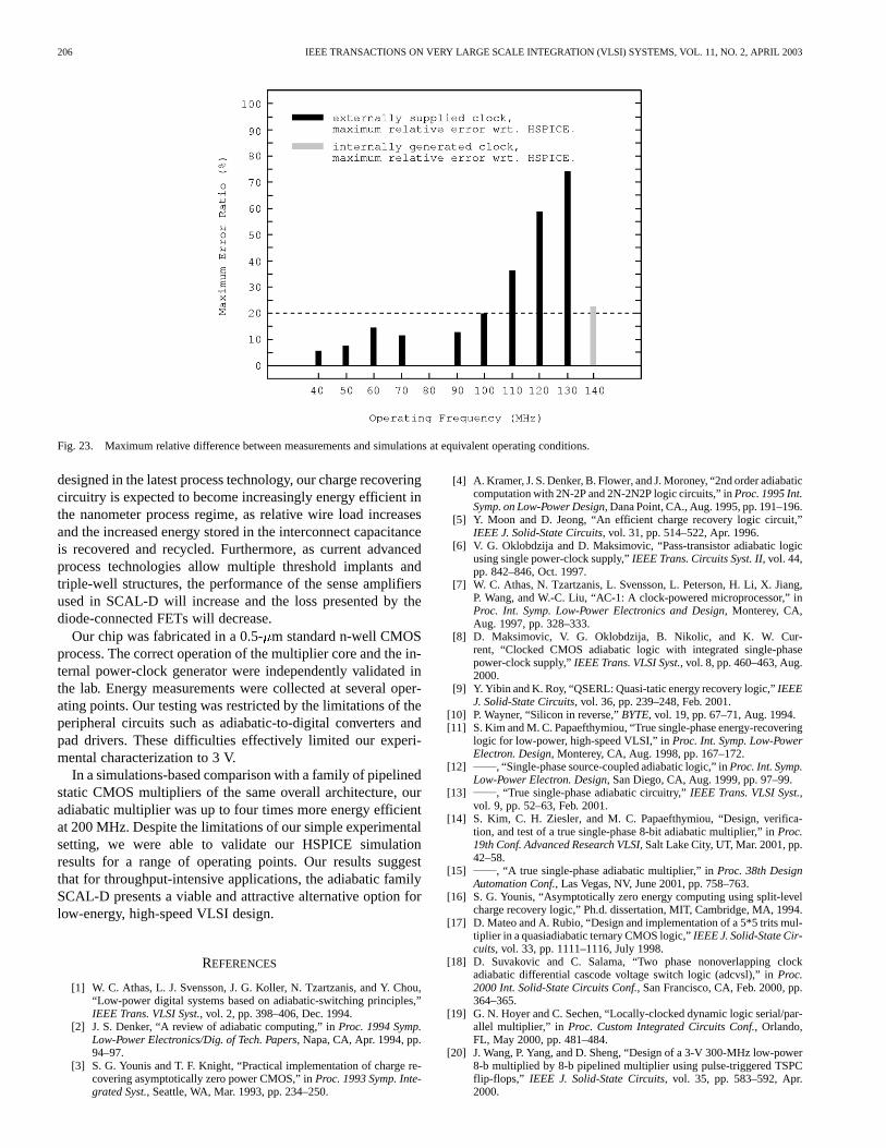
Fig. 23 shows the maximum relative difference between ourmeasurements and simulation results under the same operatingfrequencies and voltages. The externally driven power-clockmeasurements above 100 MHz suffered from relative errors ex-ceeding 20%, since the quantization and phase errors inherentin integrating the product of sampled AC voltage and currentsbecome dominant. At the direct dc measurements with the in-tegrated clock generator at 140 MHz, however, none of theseerrors exist.
VIII. C ONCLUSION
We presented the design and experimental evaluation of an8-bit adiabatic multiplier with an internal single-phase sinu-soidal power-clock generator. To provide design-for-test capa-bility, our design included built-in self-test circuitry based onbuilt-in logic block observation. Both the multiplier and theself-test circuitry were designed in SCAL-D, an adiabatic logicfamily that operates with a single-phase sinusoidal power-clock.
The adiabatic circuitry we used for our design does not relyon any particular process features. While our chip was not
206 IEEE TRANSACTIONS ON VERY LARGE SCALE INTEGRATION (VLSI) SYSTEMS, VOL. 11, NO. 2, APRIL 2003
Fig. 23. Maximum relative difference between measurements and simulations at equivalent operating conditions.
designed in the latest process technology, our charge recoveringcircuitry is expected to become increasingly energy efficient inthe nanometer process regime, as relative wire load increasesand the increased energy stored in the interconnect capacitanceis recovered and recycled. Furthermore, as current advancedprocess technologies allow multiple threshold implants andtriple-well structures, the performance of the sense amplifiersused in SCAL-D will increase and the loss presented by thediode-connected FETs will decrease.
Our chip was fabricated in a 0.5-m standard n-well CMOSprocess. The correct operation of the multiplier core and the in-ternal power-clock generator were independently validated inthe lab. Energy measurements were collected at several oper-ating points. Our testing was restricted by the limitations of theperipheral circuits such as adiabatic-to-digital converters andpad drivers. These difficulties effectively limited our experi-mental characterization to 3 V.
In a simulations-based comparison with a family of pipelinedstatic CMOS multipliers of the same overall architecture, ouradiabatic multiplier was up to four times more energy efficientat 200 MHz. Despite the limitations of our simple experimentalsetting, we were able to validate our HSPICE simulationresults for a range of operating points. Our results suggestthat for throughput-intensive applications, the adiabatic familySCAL-D presents a viable and attractive alternative option forlow-energy, high-speed VLSI design.
REFERENCES
[1] W. C. Athas, L. J. Svensson, J. G. Koller, N. Tzartzanis, and Y. Chou,“Low-power digital systems based on adiabatic-switching principles,”IEEE Trans. VLSI Syst., vol. 2, pp. 398–406, Dec. 1994.
[2] J. S. Denker, “A review of adiabatic computing,” inProc. 1994 Symp.Low-Power Electronics/Dig. of Tech. Papers, Napa, CA, Apr. 1994, pp.94–97.
[3] S. G. Younis and T. F. Knight, “Practical implementation of charge re-covering asymptotically zero power CMOS,” inProc. 1993 Symp. Inte-grated Syst., Seattle, WA, Mar. 1993, pp. 234–250.
[4] A. Kramer, J. S. Denker, B. Flower, and J. Moroney, “2nd order adiabaticcomputation with 2N-2P and 2N-2N2P logic circuits,” inProc. 1995 Int.Symp. on Low-Power Design, Dana Point, CA., Aug. 1995, pp. 191–196.
[5] Y. Moon and D. Jeong, “An efficient charge recovery logic circuit,”IEEE J. Solid-State Circuits, vol. 31, pp. 514–522, Apr. 1996.
[6] V. G. Oklobdzija and D. Maksimovic, “Pass-transistor adiabatic logicusing single power-clock supply,”IEEE Trans. Circuits Syst. II, vol. 44,pp. 842–846, Oct. 1997.
[7] W. C. Athas, N. Tzartzanis, L. Svensson, L. Peterson, H. Li, X. Jiang,P. Wang, and W.-C. Liu, “AC-1: A clock-powered microprocessor,” inProc. Int. Symp. Low-Power Electronics and Design, Monterey, CA,Aug. 1997, pp. 328–333.
[8] D. Maksimovic, V. G. Oklobdzija, B. Nikolic, and K. W. Cur-rent, “Clocked CMOS adiabatic logic with integrated single-phasepower-clock supply,”IEEE Trans. VLSI Syst., vol. 8, pp. 460–463, Aug.2000.
[9] Y. Yibin and K. Roy, “QSERL: Quasi-tatic energy recovery logic,”IEEEJ. Solid-State Circuits, vol. 36, pp. 239–248, Feb. 2001.
[10] P. Wayner, “Silicon in reverse,”BYTE, vol. 19, pp. 67–71, Aug. 1994.[11] S. Kim and M. C. Papaefthymiou, “True single-phase energy-recovering
logic for low-power, high-speed VLSI,” inProc. Int. Symp. Low-PowerElectron. Design, Monterey, CA, Aug. 1998, pp. 167–172.
[12] , “Single-phase source-coupled adiabatic logic,” inProc. Int. Symp.Low-Power Electron. Design, San Diego, CA, Aug. 1999, pp. 97–99.
[13] , “True single-phase adiabatic circuitry,”IEEE Trans. VLSI Syst.,vol. 9, pp. 52–63, Feb. 2001.
[14] S. Kim, C. H. Ziesler, and M. C. Papaefthymiou, “Design, verifica-tion, and test of a true single-phase 8-bit adiabatic multiplier,” inProc.19th Conf. Advanced Research VLSI, Salt Lake City, UT, Mar. 2001, pp.42–58.
[15] , “A true single-phase adiabatic multiplier,” inProc. 38th DesignAutomation Conf., Las Vegas, NV, June 2001, pp. 758–763.
[16] S. G. Younis, “Asymptotically zero energy computing using split-levelcharge recovery logic,” Ph.d. dissertation, MIT, Cambridge, MA, 1994.
[17] D. Mateo and A. Rubio, “Design and implementation of a 5*5 trits mul-tiplier in a quasiadiabatic ternary CMOS logic,”IEEE J. Solid-State Cir-cuits, vol. 33, pp. 1111–1116, July 1998.
[18] D. Suvakovic and C. Salama, “Two phase nonoverlapping clockadiabatic differential cascode voltage switch logic (adcvsl),” inProc.2000 Int. Solid-State Circuits Conf., San Francisco, CA, Feb. 2000, pp.364–365.
[19] G. N. Hoyer and C. Sechen, “Locally-clocked dynamic logic serial/par-allel multiplier,” in Proc. Custom Integrated Circuits Conf., Orlando,FL, May 2000, pp. 481–484.
[20] J. Wang, P. Yang, and D. Sheng, “Design of a 3-V 300-MHz low-power8-b multiplied by 8-b pipelined multiplier using pulse-triggered TSPCflip-flops,” IEEE J. Solid-State Circuits, vol. 35, pp. 583–592, Apr.2000.

KIM et al.: A TRUE SINGLE-PHASE ENERGY-RECOVERY MULTIPLIER 207
[21] G. Ma and F. J. Taylor, “Multiplier policies for digital signal processing,”IEEE ASAP Mag., vol. 7, pp. 6–19, Jan. 1990.
[22] C. F. Law, S. S. Rofail, and K. S. Yeo, “A low-power 16� 16-b parallelmultiplier utilizing pass-transistor logic,”IEEE J. Solid-State Circuits,vol. 34, pp. 1395–1399, Oct. 1999.
[23] I. S. Abu-Khater, A. Bellaouar, and M. I. Elmasry, “Circuit techniquesfor CMOS low-power high-performance multipliers,”IEEE J. Solid-State Circuits, vol. 31, pp. 1535–1546, Oct. 1996.
[24] G. N. Hoyer, G. Yee, and C. Sechen, “Locally-clocked dynamic logic,”in Proc. IEEE Midwest Symp. Circuits and Systems, Notre Dame, IN,Aug. 1998, pp. 10–12.
[25] J. M. Rabaey, Digital Integrated Circuits: A Design Perspec-tive. Englewood Cliffs, NJ: Prentice-Hall, 1996.
[26] B. Koenemann, J. Mucha, and G. Zwiehoff, “Built-in logic block ob-servation techniques,” inProc. 1979 Test Conf., Washington, DC, Sept.1979, pp. 37–41.
[27] M. Abramovici, M. A. Breuer, and A. D. Friedman,Digital SystemTesting and Testable Design. Piscataway, NJ: IEEE Press, 1990.
[28] N. O. Sokal and A. D. Sokal, “Class E—A new class of high-efficiencytuned single-ended switching power amplifiers,”IEEE J. Solid-StateCircuits, vol. SC-10, pp. 168–176, June 1975.
[29] C. H. Ziesler, S. Kim, and M. C. Papaefthymiou, “A power-clockgenerator for true single-phase adiabatic logic,” inProc. Int. Symp.Low-Power Electron. Design, Huntington Beach, CA, Aug. 2001, pp.159–164.
Suhwan Kim (S’97–M’01) received the B.S. andM.S. degrees in electrical engineering and computerscience from Korea University, Seoul, Korea, in1990 and 1992, respectively, and the Ph.D. degreein electrical engineering and computer science fromthe University of Michigan, Ann Arbor, in 2001.
From 1993 to 1997, he was with LG Electronics,Seoul, Korea, where he designed several multimediasystems-on-a-chip (SOC), including an MPEG2,CODEC for audio, video systems. In 2001, hejoined IBM T. J. Watson Research Center, Yorktown
Heights, NY, where he is currently a Research Staff Member. His researchinterests include high-performance and low-power circuits and technologyand low-power design methodologies for high-performance VLSI signalprocessing.
Dr. Kim received the 1994 Best Student Paper Award of the IEEE Korea Sec-tion, and the First Prize in the VLSI Design Contest of the 2001 ACM/IEEE De-sign Automation Conference. He has participated on the organizating committeeand the technical program committee of the IEEE International ASIC/SOC Con-ference and on the technical committee of the International Symposium on Low-power Electronics and Designs.
Conrad H. Ziesler (S’99) received the B.S. degree inelectrical engineering from the California Institute ofTechnology, Pasadena, in 1999 and the M.S. degreein electrical engineering and computer science fromthe University of Michigan, Ann Arbor, in 2002. He iscurrently pursuing the Ph.D. degree at the Universityof Michigan, Ann Arbor.
His research interests include energy recoveringcircuits for low-energy and high-performanceVLSI systems, as well as parallel architectures andalgorithms for scientific computing.
Mr. Ziesler received the First Prize in the VLSI Design Contest of the 32ndACM/IEEE Design Automation Conference and a NSF Graduate ResearchHonorable Mention.
Marios C. Papaefthymiou (M’93–SM’02) receivedthe B.S. degree in electrical engineering from theCalifornia Institute of Technology in 1988 and theS.M. and Ph.D. degrees in electrical Eengineeringand computer science from the MassachusettsInstitute of Technology, Cambridge, in 1990 and1993, respectively.
After a three-year term as an Assistant Professorat Yale University, he joined the University ofMichigan, where he is currently an AssociateProfessor of electrical engineering and computer
science and Director of the Advanced Computer Architecture Laboratory. Hisresearch interests include algorithmic, architectural, and circuit issues in thedesign of very large scale integration systems with a primary focus on energyand timing optimization. He is also active in the field of parallel and distributedcomputing.
Dr. Papaefthymiou received an ARO Young Investigator Award, an NSF CA-REER Award, and several IBM Partnership Awards. With his students, he hasreceived a Best Paper Award in the 32nd ACM/IEEE Design Automation Con-ference and the First Prize (Operational Category) in the VLSI Design Con-test of the 38th ACM/IEEE Design Automation Conference. He is an asso-ciate editor for the IEEE TRANSACTIONS ON THECOMPUTER-AIDED DESIGN
OF INTEGRATED CIRCUITS, IEEE TRANSACTIONS ON COMPUTERS, and IEEETRANSACTIONS ON VLSI SYSTEMS. He has served as the General Chair andas the Technical Program Chair for the ACM/IEEE International Workshopon Timing Issues in the Specification and Synthesis of Digital Systems. Hehas also participated several times in the Technical Program Committee of theIEEE/ACM International Conference on Computer-Aided Design.