a user comment draft standard of the joint committee on...
TRANSCRIPT

A User Comment Draft Standard of the Joint Committee on the ATC
Ballot Copy for Joint Adoption by AASHTO, ITE, and NEMA
ATC 2070 v02.03
Advanced Transportation Controller (ATC) Standard for the Type 2070 Controller
March 12, 2004
This is a draft document, which is distributed for review and ballot purposes only. You may reproduce and distribute this document within your organization, but only for the purposes of and only to the extent necessary to facilitate review and ballot to AASHTO, ITE, or NEMA. Please ensure that all copies reproduced or distributed bear this legend. This document contains recommended information which is subject to approval.
Published by American Association of State Highway and Transportation Officials (AASHTO) 444 North Capitol St., N.W., Suite 249 Washington, DC, 20001 Institute of Transportation Engineers (ITE) 1099 14th St. N.W., Suite 300 West Washington, DC, 20005-3438 National Electrical Manufacturers Association (NEMA) 1300 N. 17th Street, Suite 1847 Rosslyn, Virginia 22209-3801 © Copyright 2001-2004 AASHTO/ ITE / NEMA. All rights reserved.

Standard for the ATC – Type 2070 March 12, 2004 2
Joint NEMA, AASHTO, and ITE Copyright and
Advanced Transportation Controller (ATC) Type 2070 Controller
NOTICE
These materials are delivered "AS IS" without any warranties as to their use or performance. AASHTO/ITE/NEMA AND THEIR SUPPLIERS DO NOT WARRANT THE PERFORMANCE OR RESULTS YOU MAY OBTAIN BY USING THESE MATERIALS. AASHTO/ITE/NEMA AND THEIR SUPPLIERS MAKE NO WARRANTIES, EXPRESSED OR IMPLIED, AS TO NON-INFRINGEMENT OF THIRD PARTY RIGHTS, MERCHANTABILITY, OR FITNESS FOR ANY PARTICULAR PURPOSE. IN NO EVENT WILL AASHTO, ITE, OR NEMA OR THEIR SUPPLIERS BE LIABLE TO YOU OR ANY THIRD PART FOR ANY CLAIM OR FOR ANY CONSEQUENTIAL, INCIDENTAL, OR SPECIAL DAMAGES, INCLUDING ANY LOST PROFITS OR LOST SAVINGS, ARISING FROM YOUR REPRODUCTION OR USE OF THESE MATERIALS. EVEN IF AN AASHTO, ITE, OR NEMA REPRESENTATIVE HAS BEEN ADVISED OF THE POSSIBILITY OF SUCH DAMAGES. Some states or jurisdictions do not allow the exclusion or limitation of incidental, consequential, or special damages, or exclusion of implied warranties, so the above limitations may not apply to you. Use of these materials do not constitute an endorsement or affiliation by or between AASHTO, ITE, or NEMA and you, your company, or your products and services. If you are not willing to accept the foregoing restrictions, you should immediately return these materials. ATC is a trademark of NEMA/AASHTO/ITE.
Standard for the ATC – Type 2070 March 12, 2004 3
Revision Notes December 13, 2002 – Inserted notice of relationship between ATC 2070 Standard and the
Caltrans TEES, added Revision Notes, and renumbered Table of Contents. January 12, 2004 – Revised ATC 2070 Standard to reflect the information contained in
the Caltrans TEES dated August 16, 2002 along with Erratum 1 dated October 27, 2003, and renumbered Table of Contents.
March 12, 2004 – Revised ATC 2070 Standard to reflect the resolution of ATC
Controller Unit Working Group comments.

Standard for the ATC – Type 2070 March 12, 2004 4
Table of Contents
1 FOREWORD...............................................................................................................8 2 INTRODUCTION.......................................................................................................9
2.1 Overview..................................................................................................................9 2.2 Controllers................................................................................................................9 2.3 Controller Housing.................................................................................................10 2.4 CPU Module ..........................................................................................................10 2.5 Field I/O Module....................................................................................................10 2.6 Front Panel Module................................................................................................10 2.7 Power Supply Module............................................................................................10 2.8 VME Cage Assembly ............................................................................................11 2.9 Communications Modules .....................................................................................11 2.10 NEMA Interface.....................................................................................................11
3 GENERAL ATC REQUIREMENTS......................................................................12 3.1 General...................................................................................................................12
3.1.1 References.....................................................................................................12 3.1.2 Interchangeability .........................................................................................12 3.1.3 Documentation..............................................................................................12 3.1.4 Packaging......................................................................................................14 3.1.5 Delivery.........................................................................................................14 3.1.6 Metals............................................................................................................14 3.1.7 Mechanical Hardware ...................................................................................14 3.1.8 Electrical Isolation ........................................................................................15 3.1.9 Daughter Boards ...........................................................................................15
3.2 Components ...........................................................................................................15 3.2.1 General..........................................................................................................15 3.2.2 Electronic Components.................................................................................15 3.2.3 Capacitors .....................................................................................................16 3.2.4 Potentiometers...............................................................................................16 3.2.5 Resistors........................................................................................................16 3.2.6 Semiconductor Devices ................................................................................17 3.2.7 Transformers and Inductors ..........................................................................17 3.2.8 Triacs.............................................................................................................17 3.2.9 Circuit Breakers ............................................................................................17 3.2.10 Fuses .............................................................................................................18 3.2.11 Switches ........................................................................................................18 3.2.12 Terminal Blocks............................................................................................18 3.2.13 Screw Lug and Cam Driven Connectors ......................................................19 3.2.14 Wiring, Cabling, and Harnesses....................................................................19 3.2.15 Indicators and Character Displays ................................................................20 3.2.16 Connectors ....................................................................................................20 3.2.17 Surge Protection Device ...............................................................................22
3.3 Mechanical Requirements......................................................................................22 3.3.1 Assemblies ....................................................................................................22

Standard for the ATC – Type 2070 March 12, 2004 5
3.3.2 Locking Devices ...........................................................................................22 3.3.3 PCB Design and Connectors.........................................................................22 3.3.4 Model and Serial Numbers ...........................................................................23 3.3.5 Workmanship................................................................................................23 3.3.6 Tolerances .....................................................................................................23
3.4 Engineering ............................................................................................................23 3.4.1 Human Engineering ......................................................................................23 3.4.2 Design Engineering.......................................................................................24 3.4.3 Generated Noise............................................................................................24
3.5 Printed Circuit Boards............................................................................................24 3.5.1 Design, Fabrication, and Mounting ..............................................................24 3.5.2 Soldering.......................................................................................................26 3.5.3 Definitions.....................................................................................................26 3.5.4 Jumpers .........................................................................................................26
3.6 Quality Control ......................................................................................................27 3.6.1 Components ..................................................................................................27 3.6.2 Subassembly, Unit, or Module......................................................................27 3.6.3 Pre-delivery Repair .......................................................................................27
3.7 Electrical, Environmental, and Testing Requirements ..........................................27 3.7.1 General..........................................................................................................27 3.7.2 Inspection......................................................................................................28 3.7.3 Testing Certification .....................................................................................28 3.7.4 Definitions of Major Units of the Cabinet Assembly ...................................29 3.7.5 Environmental and Operating Requirements................................................29 3.7.6 Test Facilities ................................................................................................32 3.7.7 Test Procedure: Transients, Temperature, Voltage, and Humidity ..............32 3.7.8 Vibration Test ...............................................................................................38 3.7.9 Shock (Impact) Test......................................................................................40 3.7.10 Power Interruption Test Procedures..............................................................43 3.7.11 Cabinet Assembly Tests................................................................................43 3.7.12 Controller Unit Tests.....................................................................................45 3.7.13 Cabinet Monitor Unit Tests ..........................................................................45 3.7.14 Auxiliary Monitor Unit Tests........................................................................46 3.7.15 Power Distribution Assembly Tests..............................................................46 3.7.16 Switch Pack Tests .........................................................................................46 3.7.17 Flasher Tests .................................................................................................46 3.7.18 Flash Transfer Relay Tests............................................................................46 3.7.19 Loop Detector Unit Tests..............................................................................46 3.7.20 Serial Interface Unit Tests ............................................................................47
4 TYPE 2070 CONTROLLER UNIT.........................................................................48 4.1 General...................................................................................................................48
4.1.1 Module Descriptions.....................................................................................48 4.1.2 Unit Configuration ........................................................................................48 4.1.3 Metalwork .....................................................................................................50 4.1.4 Power Fail and Power Restoration Operation...............................................50 4.1.5 Power Limitations.........................................................................................50

Standard for the ATC – Type 2070 March 12, 2004 6
4.1.6 EIA-485 Communications Circuitry.............................................................50 4.1.7 EIA-485 Line Drivers/Receivers ..................................................................51 4.1.8 Sockets ..........................................................................................................51 4.1.9 SDLC ............................................................................................................51
4.2 Type 2070-1 CPU Module.....................................................................................51 4.2.1 Type 2070 – 1A Configuration .....................................................................51 4.2.2 Type 2070 – 1B Configuration .....................................................................51 4.2.3 Main Controller Board (MCB) .....................................................................52 4.2.4 Transition Board ...........................................................................................54 4.2.5 Shielded Interface Harness ...........................................................................55 4.2.6 Datakey .........................................................................................................55 4.2.7 CPU Module Software..................................................................................56
4.3 Type 2070-2 Field I/O Module (FI/O)...................................................................73 4.3.1 Type 2070-2A Module..................................................................................73 4.3.2 Type 2070-2B Module..................................................................................73 4.3.3 Field Controller Unit (FCU) .........................................................................73 4.3.4 Parallel I/O Ports...........................................................................................73 4.3.5 Other Module Circuit Functions ...................................................................74 4.3.6 Serial Communications/Logic Circuitry .......................................................75 4.3.7 Buffers...........................................................................................................76 4.3.8 I/O Functions ................................................................................................77 4.3.9 Data Communications Protocols...................................................................79
4.4 Type 2070-3 Front Panel Assembly ......................................................................88 4.4.1 General..........................................................................................................88 4.4.2 Keyboards .....................................................................................................89 4.4.3 CPU Active Indicator....................................................................................89 4.4.4 Display ..........................................................................................................89 4.4.5 FPA Controller..............................................................................................90 4.4.6 Electronic Bell ..............................................................................................93
4.5 Type 2070-4 Power Supply Module ......................................................................93 4.5.1 General..........................................................................................................93 4.5.2 Module Front ................................................................................................93 4.5.3 Input Protection.............................................................................................93 4.5.4 +5VDC Standby Power ................................................................................94 4.5.5 Monitor Circuitry ..........................................................................................94 4.5.6 Power Supply Requirements.........................................................................95
4.6 Unit Chassis and Type 2070-5 VME Cage Assembly...........................................96 4.6.1 General..........................................................................................................96 4.6.2 Serial Motherboard .......................................................................................96 4.6.3 Type 2070-5 VME Cage Assembly..............................................................97 4.6.4 Type 2070-1A CPU Main Controller Board.................................................97
4.7 Chapter Details.......................................................................................................97 5 TYPE 2070 PERIPHERAL EQUIPMENT ............................................................99
5.1 Type 2070-6 A & B Async/Modem Serial Comm Modules .................................99 5.1.1 Power Requirements .....................................................................................99 5.1.2 Logic Switches..............................................................................................99

Standard for the ATC – Type 2070 March 12, 2004 7
5.1.3 Circuitry ......................................................................................................100 5.1.4 Control Switch ............................................................................................101
5.2 Type 2070-7A & 7B Async Serial Comm Module .............................................101 5.2.1 Circuitry ......................................................................................................101 5.2.2 2070 -7A .....................................................................................................101 5.2.3 2070 - 7B.....................................................................................................101 5.2.4 Indicators.....................................................................................................101
5.3 Reserved for Future 2070-6D Fiber Optic Module..............................................101 5.4 Reserved for Future 2070-6E Ethernet Module...................................................101 5.5 Chapter Details.....................................................................................................102
6 NEMA MODULE....................................................................................................103 6.1 Type 2070N Controller Unit................................................................................103
6.1.1 General........................................................................................................103 6.1.2 Type 2070 (V orL) N1 Controller Unit.......................................................103 6.1.3 Type 2070 (V or L) N2 Controller Unit......................................................103 6.1.4 Serial Port 5 Frame Address .......................................................................103
6.2 2070-2N FIELD I/O MODULE...........................................................................103 6.2.1 Interfaces.....................................................................................................103 6.2.2 Type 2070-2N Module Requirements ........................................................104 6.2.3 Physical .......................................................................................................104 6.2.4 Power ..........................................................................................................104 6.2.5 Serial Port 3 Isolation..................................................................................104 6.2.6 FCU Output.................................................................................................104 6.2.7 Connector Pin Assignments........................................................................104 6.2.8 TS2 BIU Control.........................................................................................105
6.3 2070-4N (A or B) POWER SUPPLY MODULE................................................105 6.3.1 Requirements ..............................................................................................105
6.4 Type 2070- 8 Field I/O Module ...........................................................................105 6.4.1 Type 2070-8 Field I/O Module ...................................................................105 6.4.2 Module Front Panel.....................................................................................106 6.4.3 Label ...........................................................................................................106 6.4.4 Module Power Supply.................................................................................106 6.4.5 Incoming AC Power ...................................................................................106 6.4.6 Module PC Boards......................................................................................106 6.4.7 Power Down, NRESET, and LINESYNC..................................................107 6.4.8 Compliance with Type 2070-2 Field I/O Requirements.............................107 6.4.9 EIA-232 Serial Port.....................................................................................107 6.4.10 HAR 2 Harness ...........................................................................................107 6.4.11 Fault and Voltage Monitor..........................................................................107
6.5 Chapter Details.....................................................................................................109 7 GLOSSARY.............................................................................................................110
7.1.1 Terms and Abbreviations............................................................................110
Standard for the ATC – Type 2070 March 12, 2004 8
1 FOREWORD The purpose of this document is to define the standard for a multi-purpose Advanced Transportation Controller (ATC) – Type 2070 Controller. The effort to develop standards for the ATC began with the Federal Highway Administration gathering together a group of users interested in furthering the development of open architecture hardware and software to meet the future needs of Intelligent Transportation Systems. The ATC users group gained the support of the Institute of Transportation Engineers to continue their work in developing standards for the ATC. The American Association of State Highway and Transportation Officials (AASHTO) and the National Electrical Manufacturer’s Association joined with ITE to create a joint effort In July, 1999, a formal agreement was reached among NEMA, ITE and AASHTO to jointly develop, approve and maintain the ATC standards. Under the guidance of a Joint AASHTO/ITE/NEMA Committee on the ATC, a Working Group was created in order to develop a standard for the Advanced Transportation Controller. The first official meeting of this working group was in September,1999. In preparation of this Standards Publication, input of users and other interested parties was sought and evaluated. Inquiries, comments and proposed or recommended revisions should be submitted to:
Standards Engineer Institute of Transportation Engineers 1099 14th St. NW, Suite 300 West Washington, DC 20005-3483 voice: 202-298-0222 fax: 202-298-7722 email: [email protected]
Standard for the ATC – Type 2070 March 12, 2004 9
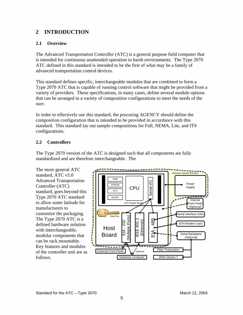
2 INTRODUCTION 2.1 Overview The Advanced Transportation Controller (ATC) is a general purpose field computer that is intended for continuous unattended operation in harsh environments. The Type 2070 ATC defined in this standard is intended to be the first of what may be a family of advanced transportation control devices. This standard defines specific, interchangeable modules that are combined to form a Type 2070 ATC that is capable of running control software that might be provided from a variety of providers. These specifications, in many cases, define several module options that can be arranged in a variety of composition configurations to meet the needs of the user. In order to effectively use this standard, the procuring AGENCY should define the composition configuration that is intended to be provided in accordance with this standard. This standard lay out sample compositions for Full, NEMA, Lite, and ITS configurations. 2.2 Controllers The Type 2070 version of the ATC is designed such that all components are fully standardized and are therefore interchangeable. The The more general ATC standard, ATC v5.0 Advanced Transportation Controller (ATC) standard, goes beyond this Type 2070 ATC standard to allow some latitude for manufacturers to customize the packaging. The Type 2070 ATC is a defined hardware solution with interchangeable, modular components that can be rack mountable. Key features and modules of the controller unit are as follows.
RAM
EPROM
RTC
DUART
CPU
Ser
ial I
/O
ATC Engine Board
Serial Interface Units
EIA
- 48
5
2070 Modem Card
Serial Backplane(Optional)
EIA
- 232
(Mul
tiple
Por
ts)
Fiber Transceiver
Other Device ?
IEE
E 8
02.3
(Eth
erne
t)
Notebook Computer
External Front Panel
InternalFront Panel(Optional)
PowerSupply
Data Key
HostBoard
Minimum System Boundry
Optional

Standard for the ATC – Type 2070 March 12, 2004 10
2.3 Controller Housing The Type 2070 controller defines a controller housing that is intended to fit an EIA 19” rack mounted form commonly found in the Type 332 and ITS family of cabinets. A NEMA base module is defined for those NEMA TS1 and TS2 shelf mounted applications. 2.4 CPU Module The CPU module consists of the main CPU, memory, software and interfaces to the remainder of the controller. There are three CPU module configurations identified in this standard. The Type 2070-1A is a two-board configuration that has a VME-based CPU board and a Transition Board. The Type 2070-1B configuration consists of a single board module. The Type 2070-1C configuration is intended to interface with the “engine board” specified by the ATC v5.0 standard. 2.5 Field I/O Module The Field I/O Module provides a mechanism for input and output interfaces. There are three options for the Field I/O Module. The Type 2070-2A Modules is intended to provide a parallel I/O interface with the Type 332 family of cabinets using the C1S connector. The Type 2070-2B Module is intended to provide a serial I/O interface to the ITS cabinet family and the NEMA interface to TS1 cabinets. The Type 2070-2N is for the NEMA TS2 Type 1 cabinets. 2.6 Front Panel Module A controller Front Panel usually contains a keyboard and display that comprise the user field interface. The Front Panel on the Type 2070 controller is optional. This standard identifies three front panel options: the Type 2070-3A Front Panel includes a large character (4 lines of 40 characters) Liquid Crystal Display (LCD), the Type 2070-3B Front Panel includes a small character (8 lines of 40 characters) LCD, and the Type 2070-3C contains only a serial connection for interfacing with a notebook computer or some other handheld computing device. 2.7 Power Supply Module A power supply module is used to convert 120-volt power to voltages required to operate the electronics inside the Type 2070 controller unit. This power supply must meet certain minimum electrical characteristics defined herein for its intended use. This standard identifies four options for the Power Supply: The Type 2070-4A identifies a 10 ampere power supply that is needed for those cases there is a need to support the VME cage assembly, and the Type 2070-4B identifies a 3.5 ampere power supply that is typically used in the “Lite” controller configurations. The Type 2070-4N (A and B) identifies the corresponding power supplies needed to support the NEMA TS1 and TS2 standards. This, however, does not preclude a Manufacturer or an AGENCY from requiring a

Standard for the ATC – Type 2070 March 12, 2004 11
specific power supply form factor so that it is consistent across a wide range of packages that may be employed by that AGENCY. 2.8 VME Cage Assembly The VME Cage Assembly is an optional expansion module for the Type 2070 ATC. The Type 2070-5 consists of a five slot 3U VME card rack. The use of the VME Cage Assembly requires the use of the Type 2070-4A 10 ampere power supply. 2.9 Communications Modules This standard includes a variety of serial and modem communications modules. The 2070-6 series of modules are for internal modems and the Type 2070-7 series of modules are for serial communications. 2.10 NEMA Interface This standard includes requirements for an optional module to interface with the NEMA TS1 and NEMA TS2 Type 2 cabinets. The Type 2070-8 NEMA Field I/O Module is an external module that attaches to the bottom of the 2070 and provides for the typical “A,” “B,” and “C” NEMA connectors.
Standard for the ATC – Type 2070 March 12, 2004 12
3 GENERAL ATC REQUIREMENTS 3.1 General In CASE of CONFLICT, the individual chapter shall govern over this chapter. All furnished equipment shall be new and unused. Vacuum or gaseous tubes and electro-mechanical devices (unless specifically called out) shall not be used. 3.1.1 References Reference is made to the following documents:
• ITS Cabinet v01.02.15, Intelligent Transportation System (ITS) Standard Specification for Roadside Cabinets, dated May 8, 2003.
3.1.2 Interchangeability Assemblies and their associated devices shall be electrically and mechanically interchangeable at both the assembly and device levels: ASSEMBLIES ASSOCIATED DEVICES Type 2070 Controller Unit - Type 2070-1 CPU Module - Type 2070-2A & 2B Field I/O Module - Type 2070-3 Front Panel Assembly - Type 2070-4 Power Supply - Type 2070-5 VME Cage Assembly - Type 2070-6 Serial Comm Module - Type 2070-7 Serial Comm Module Type 2070-N1 Controller Unit - Type 2070 Controller Unit - Type 2070-2B Field I/O Module - Type 2070-4N Power Supply Module - Type 2070-8 NEMA Module Type 2070-N2 Controller Unit - Type 2070 Controller Unit - Type 2070-2N Field I/O Module - Type 2070-4N Power Supply Module 3.1.3 Documentation 3.1.3.1 Manuals Two copies of Manual Documentation shall be supplied for each item purchased up to 200 manuals per order. The manual shall be bound in durable covers made of either 65-

Standard for the ATC – Type 2070 March 12, 2004 13
pound stock paper or clear plastic. The manual shall be printed on 8.5 inches by 11 inches paper, with the exception that schematics, layouts, parts lists and plan details may be on 11 inches by 17 inches sheets, with each sheet neatly folded to 8.5 inches by 11 inches size. A minimum of Times New Roman or Arial 10 point font shall be used for all manual text, excluding drawings and schematics. Drawing text may use a smaller font size. . 3.1.3.2 Manual Contents Each manual shall include the following sections in the order listed: 1. Table of Contents 2. Glossary 3. Manufacturer Contact Information
a. Address b. Telephone Number c. Fax Number d. General Email Address
4. General Description 5. General Characteristics 6. Installation 7. Adjustments 8. Theory of Operation a. Systems Description (include block diagram). b. Detailed Description of Circuit Operation. 9. Maintenance
a. Preventive Maintenance. b. Trouble Analysis. c. Trouble Shooting Sequence Chart. d. Wave Forms.
e. Voltage Measurements. f. Alignment Procedures. 10. Parts List (include circuit and board designation, part type and class, power rating, component manufacturer, mechanical part manufacturer, data specification sheets for special design components and original manufacturer's part number). 11. Electrical Interconnection Details & Drawings. 12. Schematic and Logic Diagram 13. Assembly Drawings and a pictorial diagram showing physical locations and
identification of each component or part. 14. The date, serial numbers, model numbers and revision numbers of equipment
covered by the manuals shall be printed on the front cover of the manuals. 3.1.3.3 Manual Pouches Deleted

Standard for the ATC – Type 2070 March 12, 2004 14
3.1.3.4 Draft Manual A preliminary draft of the manual shall be submitted, when required, to the AGENCY for approval prior to final printing. 3.1.4 Packaging Each item delivered shall be individually packed in its own shipping container. When loose Styrofoam is used for packing the item, the item shall be sealed in a plastic bag to prevent direct contact with the Styrofoam. 3.1.5 Delivery Each item delivered for testing shall be complete, including manuals, and ready for testing. 3.1.6 Metals All sharp edges and corners shall be rounded and free of any burrs. 3.1.6.1 Aluminum Sheet shall be 63 gauge American Standard (0.060-inch) minimum thick Type 3003-H14 or Type 5052-H32 ASTM Designation B209 aluminum alloy. Rod, Bar and Extruded shall be Type 6061-T6, or equal. 3.1.6.2 Stainless Steel Sheet shall be annealed or one-quarter-hard complying with the ASTM Designation: A666 for Type 304, Grades A or B, stainless steel sheet. 3.1.6.3 Cold Rolled Steel Sheet, Rod, Bar and Extruded shall be Type 1018/1020. 3.1.6.3.1 Plating All cold roll steel shall be plated. All plating shall be either cadmium plating meeting the requirements of Federal Specification QQ-P-416C, Type 2 Class l or zinc plating meeting the requirements of ASTM B633-85 Type II SC4. 3.1.7 Mechanical Hardware All bolts, nuts, washers, screws, hinges and hinge pins shall be stainless steel unless otherwise specified.

Standard for the ATC – Type 2070 March 12, 2004 15
3.1.8 Electrical Isolation Within the circuit of any device, module, or Printed Circuit Board (PCB), electrical isolation shall be provided between DC logic ground, equipment ground and the AC- conductor. They shall be electrically isolated from each other by 500 megohms, minimum, when tested at the input terminals with 500 VDC. 3.1.9 Daughter Boards Keyboards and LCD/LED Displays are considered daughter boards. Daughter boards shall be mechanically secured with a minimum of four spacers/metal screws. Connectors shall be either Flat Cable or PCB Headers. Components are allowed to be mounted under the daughter board. 3.2 Components 3.2.1 General All components shall be second sourced and shall be of such design, fabrication, nomenclature or other identification as to be purchased from a wholesale distributor or from the component manufacturer, except as follows: 3.2.1.1 When a component is of such special design that it precludes the purchase of identical components from any wholesale distributor or component manufacturer, one spare duplicate component shall be furnished with each 20, or fraction thereof, components used. 3.2.1.2 The electronic circuit design shall be such that all components of the same generic type, regardless of manufacturer, shall function equally in accordance with the specifications. 3.2.2 Electronic Components 3.2.2.1 No device shall be socket mounted unless specifically called out. 3.2.2.2 No component shall be operated above 80% of its maximum rated voltage, current or power ratings. Digital components shall not be operated above 3% over their nominal voltage, current or power ratings.

Standard for the ATC – Type 2070 March 12, 2004 16
3.2.2.3 No component shall be provided where the manufactured date is three years older than the contract award date. The design life of all components, operating for twenty-four hours a day and operating in their circuit application, shall be ten years or longer. 3.2.2.4 Components shall be arranged so they are easily accessible, replaceable and identifiable for testing and maintenance. Where damage by shock or vibration exists, the component shall be supported mechanically by a clamp, fastener, retainer, or hold-down bracket. 3.2.2.5 The Manufacturer shall submit detailed engineering technical data on all components at the request of the AGENCY. The Manufacturer shall certify that the component application meets the requirements of this standard. 3.2.3 Capacitors The DC and AC voltage ratings as well as the dissipation factor of a capacitor shall exceed the worst-case design parameters of the circuitry by 150%. Capacitor encasements shall be resistant to cracking, peeling and discoloration. All capacitors shall be insulated and shall be marked with their capacitance values and working voltages. Electrolytic capacitors shall not be used for capacitance values of less than 1.0 microfarad and shall be marked with polarity. 3.2.4 Potentiometers Potentiometers with ratings from 1 to 2 watts shall meet Military Type RV4 requirements. Under 1 Watt potentiometers shall be used only for trimmer type function. The potentiometer power rating shall be at least 100% greater than the maximum power requirements of the circuit. 3.2.5 Resistors Fixed carbon film, deposited carbon, or composition insulated resistors shall conform to the performance requirements of Military Specifications MIL-R-11F or MIL-R-22684. All resistors shall be insulated and shall be marked with their resistance values. Resistance values shall be indicated by the EIA color codes, or stamped value. The value of the resistors shall not vary by more than 5% between -37 degrees C and 74 degrees C.
Standard for the ATC – Type 2070 March 12, 2004 17
3.2.5.1 Special ventilation or heat sinking shall be provided for all 2- watt or greater resistors. They shall be insulated from the PCB. 3.2.6 Semiconductor Devices 3.2.6.1 All transistors, integrated circuits, and diodes shall be a standard type listed by EIA and clearly identifiable. 3.2.6.2 All metal oxide semiconductor components shall contain circuitry to protect their inputs and outputs against damage due to high static voltages or electrical fields. 3.2.6.3 Device pin "1" locations shall be properly marked on the PCB adjacent to the pin. 3.2.7 Transformers and Inductors All power transformers and inductors shall have the manufacturer's name or logo and part number clearly and legibly printed on the case or lamination. All transformers and inductors shall have their windings insulated, shall be protected to exclude moisture, and their leads color coded with an approved EIA color code or identified in a manner to facilitate proper installation. 3.2.8 Triacs Each triac with a designed circuit load of greater than 0.5 Amperes at 120 VAC shall be mounted to a heat sink with thermal conductive compound or material, in addition to being mechanically secured. 3.2.9 Circuit Breakers Circuit breakers shall be listed by UL or ETL. The trip and frame sizes shall be plainly marked (marked on the breaker by the manufacturer), and the ampere rating shall be visible from the front of the breaker. Contacts shall be silver alloy and enclosed in an arc quenching chamber. Overload tripping shall not be influenced by an ambient air temperature range of from -18 degrees C to 50 degrees C. The minimum Interrupting Capacity shall be 5,000 amperes, RMS when the breaker is secondary to a UL approved fuse or primary circuit breaker and both breakers in concert provide the rated capacity. For circuit breakers 80 amperes and above, the minimum interrupting capacity shall be

Standard for the ATC – Type 2070 March 12, 2004 18
10,000 amperes, RMS. Circuit breakers shall be the trip-free type with medium trip delay characteristic (Carlingswitch Time Delay Curve #24 or equal). 3.2.9.1 Load Circuit Breaker Auxiliary Internal Switches The Load Circuit Breakers used to power Switch Packs shall have auxiliary switches. The auxiliary switches shall “open” when the load breaker has tripped and the system will transfer the power from the Main Contactor to the Flash or Blank condition. 3.2.10 Fuses All Fuses that are resident in a bayonet style fuse holder shall have the fuse size rating labeled on the holder or on the panel adjacent to the holder. Fuses shall be easily accessible and removable without use of tools. 3.2.11 Switches 3.2.11.1 Dip Dual-inline-package, quick snap switches shall be rated for a minimum of 30,000 operations per position at 50 milliamperes, 30 VDC. The switch contact resistance shall be 100 milliohms maximum at 2 milliamperes, 30 VDC. The contacts shall be gold over brass. 3.2.11.2 Logic The switch contacts shall be rated for a minimum of 1 ampere resistive load at 120 VAC and shall be silver over brass (or equal). The switch shall be rated for a minimum of 40,000 operations. 3.2.11.3 Control The switch contacts shall be rated for a minimum of 5 amperes resistive load at 120 VAC or 28 VDC and shall be silver over brass (or equal). The switch shall be rated for a minimum of 40,000 operations. 3.2.11.4 Power Ratings shall be the same as CONTROL, except the contact rating shall be a minimum of 10 amperes at 125 VAC. 3.2.12 Terminal Blocks The terminal blocks shall be barrier type, rated at 20 amperes and 600 VAC RMS minimum. The terminal screws shall be 0.3125 inchs minimum length nickel plated

Standard for the ATC – Type 2070 March 12, 2004 19
brass binder head type with screw inserts of the same material. Screw size is called out under the associated file, panel or assembly.
3.2.13 Screw Lug and Cam Driven Connectors Provided the connectors mate, screw lug cam driven devices or crimp pin connectors shall be allowable if the interface is part of a harness. For field termination, screw lug and cam driven assemblies are interchangeable for field wiring termination, provided they both accommodate 22-gauge wire on the inputs and 22-gauge wire on the outputs.
3.2.14 Wiring, Cabling, and Harnesses 3.2.14.1 Harnesses shall be neat, firm and properly bundled with external protection. They shall be tie-wrapped and routed to minimize crosstalk and electrical interference. Each harness shall be of adequate length to allow any conductor to be connected properly to its associated connector or termination point. Conductors within an encased harness have no color requirements. Printed circuit motherboards are to be used where possible to eliminate or reduce cabinet wiring. 3.2.14.2 Wiring containing AC shall be bundled separately or shielded separately from all DC logic voltage control circuits. 3.2.14.3 Wiring shall be routed to prevent conductors from being in contact with metal edges. Wiring shall be arranged so that any removable assembly may be removed without disturbing conductors not associated with that assembly. 3.2.14.4 All conductors, except those that can be readily traced, shall be labeled. Labels attached to each end of the conductor shall identify the destination of the other end of the conductor. 3.2.14.5 All conductors shall conform to MIL-W-16878E/1 or better and shall have a minimum of 19 strands of copper. The insulation shall be polyvinyl chloride with a minimum thickness of 10 mils or greater. Where insulation thickness is 15 mils or less, the conductor shall conform to MIL-W-16878/17.

Standard for the ATC – Type 2070 March 12, 2004 20
3.2.14.6 Conductor color identification shall be as follows: AC- circuits - white Equip. Ground - solid green or continuous green color with 1 or more yellow
stripes. DC logic ground - continuous white with a red stripe. AC+ circuits - continuous black or black with colored stripe. DC logic ungrounded or signal - any color not specified 3.2.15 Indicators and Character Displays All indicators and character displays shall be readily visible at a radius of up to 4 feet within the cone of visibility when the indicator is subjected to 97,000 lux (9,000 foot-candles) of white light with the light source at 45 degrees (+/-2 degrees) to the front panel. 3.2.15.1 3.2.15.2 Indicators All indicators and character displays shall have a minimum 90 degrees cone of visibility with its axis perpendicular to the panel on which the indicator is mounted. All indicators shall be self-luminous. All indicators shall have a rated life of 100,000 hours minimum. Each LED indicator shall be white or clear when off. Indicators supplied on equipment requiring handles shall be mounted such that a horizontal clearance shall be provided. 3.2.15.3 Character Displays Liquid Crystal Displays (LCD) shall be readable at temperatures of -20 degrees C to +70 degrees C. All controller unit functions are required to operate at temperatures of –37 degrees C to +74 degrees C. 3.2.16 Connectors 3.2.16.1 General Connectors shall be keyed to prevent improper insertion of the wrong connector where equipment damage or operator injury may result. The mating connectors shall be designated as the connector number and male/female relationship, such as C1P (plug or PCB edge connector) and C1S (socket).

Standard for the ATC – Type 2070 March 12, 2004 21
3.2.16.2 Type T Type T connector shall be a single row, 10 position, feed through terminal block. The terminal block shall be a barrier type with 6-32, 0.25 inches or longer, nickel plated brass binder head screws. Each terminal shall be permanently identified as to its function. 3.2.16.3 Plastic Circular and Type M Pin and socket contacts for connectors shall be beryllium copper construction subplated with 1.27 microns nickel and plated with 0.76 microns gold. Pin diameter shall be 0.0618 inches. All pin and socket connectors shall use the AMP #601105-1 or #91002-1 contact insertion tool and the AMP #305183 contact extraction tool. 3.2.16.4 Card Edge and Two-Piece PCB 3.2.16.4.1 Edge connectors shall have bifurcated gold-plated contacts. The PCB receptacle connector shall meet or exceed the following: Operating Voltage: 600 VAC (RMS) Current Rating: 5.0 Amperes Insulation Material: Diallyl Phthalate or Thermoplastic Insulation Resistance: 5,000 Megohms Contact Material: Copper alloy plated with 0.00005 inches of nickel and 0.000015 inches of gold Contact Resistance: 0.006 Ohm maximum 3.2.16.4.2 The two-piece PCB connector shall meet or exceed the DIN 41612. 3.2.16.4.3 The PCB 22/44 Connector shall have 22 independent contacts per side; dual sided with 0.156 inch contact centers. 3.2.16.5 Wire Terminal Each wire terminal shall be solderless with PVC insulation and a heavy duty short -locking spade type connector. All terminal connectors shall be crimped using a Controlled-Cycle type crimping tool. 3.2.16.6 Flat Cable Each flat cable connector shall be designed for use with 26 AWG cable; shall have dual cantilevered phosphor bronze contacts plated with 0.00015 inches of gold over 0.00005

Standard for the ATC – Type 2070 March 12, 2004 22
inches of nickel; and shall have a current rating of 1 Ampere minimum and an insulation resistance of 5 Megohms minimum. 3.2.16.7 PCB Header Post Each PCB header post shall be 0.025 inches square by 0.3425 inches high from the plane of the PCB to the end of the pin; shall be mounted on 0.10 inch centers; and shall be tempered hard brass plated with 0.00015 inches of gold over 0.00005 inches of nickel. 3.2.16.8 PCB Header Socket Each PCB header socket block shall be nylon or diallyl phthalate. Each PCB header socket contact shall be removable, but crimp-connected to its conductor. The Manufacturer shall list the part number of the extraction tool recommended by its manufacturer. Each PCB header socket contact shall be brass or phosphor bronze plated with 0.0015 inches of gold over 0.00005 inches of nickel. 3.2.17 Surge Protection Device The surge suppression device shall comply with ANSI/IEEE C62.41 (100 Kilohertz Ring Wave, the 1.2/50 microseconds – 8/20 Combination Wave and the EFT Burst) at voltages and currents specified at “Location Category B2” and at “Test Severity” level III (i.e. up to 4.0 Kilovolts, open-circuit). 3.3 Mechanical Requirements 3.3.1 Assemblies All assemblies shall be modular, easily replaceable and incorporate plug-in capability for their associated devices or PCBs. Assemblies shall be provided with two guides for each plug-in PCB or associated device (except relays). The guides shall extend to within 0.75 inches from the face of either the socket or connector and front edge of the assembly. If Nylon guides are used, the guides shall be securely attached to the file or assembly chassis. 3.3.2 Locking Devices All screw type fasteners shall utilize locking devices or locking compounds except for finger screws, which shall be captive. 3.3.3 PCB Design and Connectors No components, traces, brackets or obstructions shall be within 0.125 inches of the board edge (guide edges). The manufacturer's name or logo, model number, serial number, and circuit issue or revision number shall appear and be readily visible on all PCBs.
Standard for the ATC – Type 2070 March 12, 2004 23
3.3.4 Model and Serial Numbers 3.3.4.1 The manufacturer's model number, and circuit issue or revision number shall appear on the rear panel of all equipment supplied (where such panel exists). In addition to any assignment of model numbers by the manufacturer, the TYPE number shall be displayed on the front panel in bold type, at least 0.25 inches high. 3.3.4.2 A permanent label shall be affixed to the inside near and center floor of the Type 2070 unit chassis when viewed from the front. The label shall display the unit's serial number. The number shall be permanent and easy to read. 3.3.5 Workmanship Workmanship shall conform to the requirements of this specification and be in accordance with the highest industry standards. 3.3.6 Tolerances The following tolerances shall apply, except as specifically shown on the plans or in these specifications: TYPE DIMENSIONAL TOLERANCE Sheet Metal +/-0.0525 inch PCB +0 inch, - 0.010 inch Edge Guides +/-0.015 inch *Note: These dimensional tolerances do not apply to material gauge or thickness. 3.4 Engineering The equipment shall be engineered for simplicity, ease of operation and maintenance. 3.4.1 Human Engineering 3.4.1.1 The equipment shall be engineered for simplicity, ease of operation and maintenance.
Standard for the ATC – Type 2070 March 12, 2004 24
3.4.1.2 Knobs shall be a minimum of 0.5 inches in diameter and a minimum separation of 0.5 inches edge to edge. 3.4.1.3 PCBs shall slide smoothly in their guides while being inserted into or removed from the frame and shall fit snugly into the plug-in PCB connectors. PCBs shall require a force no less than 5 pounds-force or greater than 50 pounds-force for insertion or removal. 3.4.2 Design Engineering The design shall be inherently temperature compensated to prevent abnormal operation. The circuit design shall include such compensation as is necessary to overcome adverse effects due to temperature in the specified environmental range. The design shall take into consideration the protection of personnel from all dangerous voltages. 3.4.3 Generated Noise No item, component or subassembly shall emit an audible noise level exceeding the peak level of 55 dBa when measured at a distance of one meter away from its surface, except as otherwise noted. No item, component or subassembly shall emit a noise level sufficient to interfere with processing and communication functions of the controller circuits. 3.5 Printed Circuit Boards 3.5.1 Design, Fabrication, and Mounting 3.5.1.1 All contacts on PCBs shall be plated with a minimum thickness of 0.00003 inches gold over a minimum thickness of 0.000075 inches nickel. 3.5.1.2 PCB design shall be such that when a component is removed and replaced, no damage is done to the board, other components, conductive traces or tracks. 3.5.1.3 Fabrication of PCBs shall be in compliance with Military Specification MIL-P-13949, except as follows:

Standard for the ATC – Type 2070 March 12, 2004 25
3.5.1.3.1 NEMA FR-4 glass cloth base epoxy resin copper clad laminates 0.0625 inches minimum thickness shall be used. Inter-component wiring shall be by laminated copper clad track having a minimum weight of 0.2 ounces per square foot with adequate cross section for current to be carried. All copper tracks shall be plated or soldered to provide complete coverage of all exposed copper tracks. Jumper wires to external PCB components shall be from plated-through padded holes and as short as possible. 3.5.1.3.2 All PCBs shall conform to Section 3.3 of Military Specification MIL-P-13949G Grade of Pits and Dents shall be of Grade B quality (3.5.1.3) or better. The class of permissible bow or twist shall be Class C (Table V) or better. The class of permissible warp or twist shall be Class A (Table II) or better. 3.5.1.3.3 Sections 4.2 through 6.6 of Military Specification MIL-P-13949G (inclusive) shall be omitted except as referenced in previous sections of this specification. 3.5.1.4 The mounting of parts and assemblies on the PCB shall conform to Military Specification MIL-STD-275E, except as follows: 3.5.1.4.1 Semiconductor devices that dissipate more than 250 milliwatts or cause a temperature rise of 10 degrees C or more shall be mounted with spacers, transipads or heat sinks to prevent contact with the PCB. 3.5.1.4.2 When completed, all residual flux shall be removed from the PCB. 3.5.1.4.3 The resistance between any two isolated, independent conductor paths shall be at least 100 Megohms when a 500 VDC potential is applied. 3.5.1.4.4 All PCBs shall be coated with a moisture resistant coating.

Standard for the ATC – Type 2070 March 12, 2004 26
3.5.1.4.5 Where less than 0.25 inches lateral separation is provided between the PCB (or the components of a PCB) and any metal surface, a 0.0625 inches (+/-0.0005 inches) Thick Mylar (polyester) plastic cover shall be provided on the metal to protect the PCB. 3.5.1.5 Each PCB connector edge shall be chamfered at 30 degrees from board side planes. The key slots shall also be chamfered so that the connector keys are not extracted upon removal of board or jammed upon insertion. The key slots shall be 0.045 inches (+/-0.005 inches) for 0.1 inches spacing and 0.055 inches (+/-0.005 inches) for 0.156 inches spacing. 3.5.2 Soldering 3.5.2.1 Hand soldering shall comply with Military Specification MIL-STD-2000. 3.5.2.2 Automatic flow soldering shall be a constant speed conveyor system with the conveyor speed set at optimum to minimize solder peaks or points. Temperature shall be controlled to within +/- 8 degrees C of the optimum temperature. The soldering process shall result in the complete coverage of all copper runs, joints and terminals with solder except that which is covered by an electroplating process. Wherever clinching is not used, a method of holding the components in the proper position for the flow process shall be provided. 3.5.2.3 If exposure to the temperature bath is of such a time-temperature duration, as to come within 80% of any component's maximum specified time-temperature exposure, that component shall be hand soldered to the PCB after the flow process has been completed. 3.5.3 Definitions Definitions for the purpose of this section on PCBs shall be taken from MIL-P-55110D Section 3.3 and any current addendum. 3.5.4 Jumpers Jumpers are not allowed unless called out in the specifications or approved by the AGENCY.

Standard for the ATC – Type 2070 March 12, 2004 27
3.6 Quality Control 3.6.1 Components All components shall be lot sampled to assure a consistent high conformance standard to the design specification of the equipment. 3.6.2 Subassembly, Unit, or Module Complete electrical, environmental and timing compliance testing shall be performed on each module, unit, printed circuit or subassembly. Components will be tested as a complete controller assembly. Housing, chassis, and connection terminals shall be inspected for mechanical sturdiness, and harnessing to sockets shall be electrically tested for proper wiring sequence. The equipment shall be visually and physically inspected to assure proper placement, mounting, and compatibility of subassemblies. 3.6.3 Pre-delivery Repair 3.6.3.1 Any defects or deficiencies found by the inspection system involving mechanical structure or wiring shall be returned through the manufacturing process or special repair process for correction. 3.6.3.2 PCB flow soldering is allowed a second time if copper runs and joints are not satisfactorily coated on the first run. Under no circumstances shall a PCB be flow soldered more than twice. 3.6.3.3 Hand soldering is allowed for printed circuit repair. 3.7 Electrical, Environmental, and Testing Requirements The framework of this section 3.7, along with the specific test requirements contained herein, is excerpted with modifications from NEMA TS2-2003 - Section 2 by permission of NEMA. Excerpt © 2002 AASHTO / ITE / NEMA. 3.7.1 General This section establishes the limits of the environmental and operational conditions in which the Cabinet Assembly will perform. This section defines the minimum test procedures which may be used to demonstrate conformance of a device type with the provisions of the standard. These test procedures do not verify equipment performance

Standard for the ATC – Type 2070 March 12, 2004 28
under every possible combination of environmental requirements covered by this standard. However, nothing in this testing profile shall be construed as to relieve the requirement that the equipment provided must fully comply with these standards/specifications under all environmental conditions stated herein. Individual agencies may wish to extend the testing profile or introduce additional tests to verify compliance. (Authorized Engineering Information). 3.7.2 Inspection A visual and physical inspection shall include mechanical, dimensional and assembly conformance to all parts of this standard. 3.7.3 Testing Certification 3.7.3.1 A complete quality control / final test report shall be supplied with each item. Quality control procedures shall be submitted to the AGENCY prior to production. The test report shall indicate the name of the tester and shall be signed by a responsible manager. 3.7.3.2 The quality control procedure and test report format shall be supplied to the AGENCY for approval upon request. The quality control procedure shall include the following, in the order shown:
Design Acceptance testing of all supplied components. Physical and functional testing of all modules and items. Environmental testing report(s) for all equipment. Physical and functional testing of all items.
3.7.3.3 Separate certifications should be provided for Design and Production. Design Acceptance testing should be performed with a fully loaded and functional Cabinet Assembly meeting the requirements of this standard (Cabinet Assembly containing all of the Major Units necessary to provide a fully functional and operational Cabinet Assembly). Production testing should be performed as part of the AGENCY’s procurement delivery procedures and that testing should be performed at the Major Unit level. (Authorized Engineering Information). 3.7.3.4 Certain portions of the test procedures contained in this standard my cause damage to the unit (e.g. protection devices may be aged) and are not recommended for routine Production testing. (Authorized Engineering Information)

Standard for the ATC – Type 2070 March 12, 2004 29
3.7.4 Definitions of Major Units of the Cabinet Assembly For the purpose of this section, "Major units of the Cabinet Assembly” shall include the Controller Unit, Application Software for implementing the desired functionality, Cabinet Monitor Unit (CMU), Auxiliary Monitor Unit (AMU), Serial Interface Units (SIUs), Power Distribution Unit (PDA), Switch Packs, Flasher(s), and Detector(s). 3.7.5 Environmental and Operating Requirements The requirements (voltage, temperature, etc.) of this section shall apply in any combination. 3.7.5.1 Voltage and Frequency 3.7.5.1.1 Operating Voltage The nominal voltage shall be 120 VAC, unless otherwise noted. 3.7.5.1.2 Operating Frequency The operating frequency range shall be 60 hertz (+/-3.0 hertz), unless otherwise noted.. 3.7.5.2 Transients, Power Service The Test Unit shall maintain all defined functions when the independent test pulse levels specified in 3.7.5.2.1 and 3.7.5.2.2 occur on the alternating-current power service. 3.7.5.2.1 High-Repetition Noise Transients The test pulses shall not exceed the following conditions: 1. Amplitude: 300 Volts, both positive and negative polarity. 2. Peak Power: 2500 watts. 3. Repetition: 1 pulse approximately every other cycle moving uniformly over the full
wave in order to sweep across 360 degrees of the line cycle once every 3 seconds. 4. Pulse Rise Time: 1 microsecond. 5. Pulse Width: 10 microseconds. 6. This test is performed without protection in place or operational.
Standard for the ATC – Type 2070 March 12, 2004 30
This test is considered to be a minimum test requirement for the Test Unit complying with ANSI/IEEE C62.41. Regional conditions may warrant additional testing as described in ANSI/IEEE C62.41. (Authorized Engineering Information) 3.7.5.2.2 Low-Repetition High-Energy Transients The test pulses shall not exceed the following conditions: 1. Amplitude: 600 Volts (+/-5 percent), both positive and negative polarity. 2. Energy Source: Capacitor, oil filled, 10 microfarads (+/-10 percent), internal surge
impedance less than 1 ohm. 3. Repetition: 1 discharge every 10 seconds. 4. Pulse Position: Random across 360 degrees of the line cycle. 5. This test is performed with protection in place and operational. This test is considered to be a minimum test requirement for the Test Unit complying with ANSI/IEEE C62.41. Regional conditions may warrant additional testing as described in ANSI/IEEE C62.41. (Authorized Engineering Information) 3.7.5.3 Nondestructive Transient Immunity The Test Unit (with protection in place and operational) shall be capable of withstanding a high energy transient having the following characteristics repeatedly applied to the alternating current input terminals (no other power connected to terminals) without failure of the test specimen: 1. Amplitude: 1000 Volts (+/-5 percent), both positive and negative polarity. 2. Energy Source: Capacitor, oil filled, 15 microfarads (+/-10 percent), internal surge
impedance less than 1 ohm. 3. Repetition: Applied to the Test Unit once every 2 seconds for a maximum of three
applications for each polarity. 4. After the foregoing, the Test Unit shall perform all defined functions upon the
application of nominal alternating current power. This test is considered to be a minimum test requirement for the Test Unit complying with ANSI/IEEE C62.41 (100 Kilohertz Ring Wave, the 1.2/50 microseconds – 8/20 Combination Wave and the EFT Burst) at voltages and currents specified at “Location Category B2” and at “Test Severity” level III (i.e. up to 4.0 Kilovolts, open-circuit).

Standard for the ATC – Type 2070 March 12, 2004 31
Regional conditions may warrant additional testing as described in ANSI/IEEE C62.41. (Authorized Engineering Information) 3.7.5.4 Transients, Input-Output Terminals The Test Unit (without protection in place or operational) shall maintain all defined functions, when the test pulse occurs on the input-output terminals. 1. Amplitude: 300 Volts, both positive and negative polarity. 2. Pulse Source: 1000 ohms nominal impedance. 3. Repetition: 1 pulse per second, for a minimum of 5 pulses per selected terminal. 4. Pulse rise time: 1 microsecond. 5. Pulse width: 10 microseconds. This test is considered to be a minimum test requirement for the Test Unit complying with ANSI/IEEE C62.41. Regional conditions may warrant additional testing as described in ANSI/IEEE C62.41. (Authorized Engineering Information) 3.7.5.5 Temperature and Humidity The Test Unit shall maintain all programmed functions when the temperature and humidity ambients are within the specified limits defined herein (3.7.5.5.1 and3.7.5.5.2). 3.7.5.5.1 Ambient Temperature The operating ambient temperature range shall be from -37 degrees C to +74 degrees C. The storage temperature range shall be from -45 degrees C to +85 degrees C. The rate of change in ambient temperature shall not exceed 18 degrees C per hour, during which the relative humidity shall not exceed 95 percent. 3.7.5.5.2 Humidity The relative humidity shall not exceed 95 percent non-condensing over the temperature range of -37 degrees C to +74 degrees C. Above +46 degrees C, constant absolute humidity shall be maintained. This will result in the relative humidities shown in Exhibit 3-1 for dynamic testing.

Standard for the ATC – Type 2070 March 12, 2004 32
Exhibit 3-1 AMBIENT TEMPERATURE VERSUS RELATIVE HUMIDITY
AT BAROMETRIC PRESSURES (29.92 In. Hg.) (NON-CONDENSING)
Ambient Temperature/ Dry Bulb (in degrees C)
Relative Humidity (in percent)
Ambient Temperature/ Wet Bulb (in degrees C)
-37.0 to 1.1 10 -17.2 to 42.7 1.1 to 46.0 95 42.7
48.8 70 42.7 54.4 50 42.7 60.0 38 42.7 65.4 28 42.7 71.2 21 42.7 74.0 18 42.7
3.7.6 Test Facilities All instrumentation required in the test procedures, such as voltmeters, ammeters, thermocouples, pulse timers, etc. shall be selected in accordance with good engineering practice. In all cases where time limit tests are required, the allowance for any instrumentation errors shall be included in the limit test. 1. Variable Voltage Source: A variable source capable of supplying 20 amperes from
100 VAC to 135 VAC. 2. Environmental Chamber: An environmental chamber capable of attaining
temperatures of -37 degrees C to +74 degrees C and relative humidities given in Exhibit 3-1.
3. Transient Generator(s): Transient generator(s) capable of supplying the transients
outlined in 3.7.5.2 through 3.7.5.4. 3.7.7 Test Procedure: Transients, Temperature, Voltage, and Humidity 3.7.7.1 Test A: Placement in Environmental Chamber and Check-Out of Hook-Up 1. Place the test unit in the environmental chamber. Connect the test unit AC input
circuit to a variable voltage power transformer, voltmeter, and transient generator. The transient generator shall be connected to the AC input circuit at a point at least 25 feet from the AC power source and not over 10 feet from the input to the test unit.
2. Connect test switches to the appropriate terminals to simulate the various features
incorporated into the test unit. Place these switches in the proper position for desired operation.

Standard for the ATC – Type 2070 March 12, 2004 33
3. Verify the test hook-up. Adjust the variable-voltage power transformer to 120 VAC and apply power to the test unit. Verify that the test unit goes through its prescribed startup sequence and cycles properly in accordance with the operation determined by the positioning of test switches in item 2.
Upon the satisfactory completion and verification of the test hook-up, proceed with Test B. 3.7.7.2 Test B: Transient Tests (Power Service) 1. Program the test unit to dwell. Verify the input voltage is 120 VAC. 2. Set the transient generator to provide high-repetition noise transients as follows:
a. Amplitude: 300 Volts (+/-5 percent), both positive and negative polarity. b. Peak Power: 2500 watts. c. Repetition Rate: One pulse every other cycle moving uniformly over the full wave
in order to sweep once every 3 seconds across 360 degrees of line cycle. d. Pulse Rise Time: 1 microsecond. e. Pulse Width: 10 microseconds.
3. Apply the transient generator output to the AC voltage input for at least 5 minutes. Repeat this test for at least two conditions of dwell for the test unit. The test unit must continue to dwell without malfunction.
4. Program the test unit to cycle through normal operations. Turn on the transient
generator (output in accordance with item 2) for 10 minutes, during which time the test unit shall continue to cycle without malfunction.
5. Set a transient generator to provide high-repetition noise transients as follows:
a. Amplitude: 300 Volts (+/-5 percent), both positive and negative polarity. b. Source Impedance: Not less than 1000 ohms nominal impedance. c. Repetition: One pulse per second for a minimum of five pulses per selected
terminal. d. Pulse Rise Time: 1 microsecond. e. Pulse Width: 10 microseconds. Program the test unit to dwell. Verify the input voltage is 120 VAC.
6. Apply the transient generator (output in accordance with item 5) between logic ground and the connecting cable termination of selected Field I/O input/output terminals of the test unit. A representative sampling of selected input/output terminations shall be tested. The test unit shall continue to dwell without malfunction.

Standard for the ATC – Type 2070 March 12, 2004 34
7. Program the test unit to cycle. Turn on the transient generator (output in accordance with item 5) and apply its output to the selected Field I/O input/output terminations. The test unit shall continue to cycle without malfunction.
8. Reinstall protection and set a transient generator to provide low-repetition high-
energy transients as follows: a. Amplitude: 600 Volts (+/-5 percent), both positive and negative polarity. b. Energy Discharge Source: Capacitor, oil-filled, 10 microfarads. c. Repetition Rate: One discharge each 10 seconds. d. Pulse Position: Random across 360 degrees of line cycle.
9. Program the test unit to dwell. Verify the input voltage is 120 VAC. 10. Discharge the oil-filled 10-microfarad capacitor ten times for each polarity across the
AC voltage input. Repeat this test for at least two conditions of dwell. The test unit shall continue to dwell without malfunction.
11. Program the test unit to cycle through normal operations. Discharge the capacitor ten
times for each polarity while the test unit is cycling, during which time the test unit shall continue to cycle without malfunction.
12. During the preceding transient tests (item 3 through 11), the test unit must continue
its programmed functions. The test unit shall not skip normal program intervals/steps or portions thereof when in normal operation; place false inputs or produce false outputs while in dwell; disrupt normal sequences in any manner; or change parameters.
13. Nondestructive Transient Immunity: a. Turn off the AC power input to the test unit from the variable-voltage power
source. b. Apply the following high-energy transient to the AC voltage input terminals of
the test unit (no other power connected to terminals): (1) Amplitude: 1000 V, both positive and negative polarity. (2) Peak Power Discharge: Capacitor, oil-filled, 15 microfarads. (3) Maximum Repetition Rate: Applied to the Cabinet Assembly once every 2
seconds for a maximum of three applications for each polarity. c. Upon completion of the foregoing, apply 120 VAC to the test unit and verify that
the test unit goes through its prescribed startup sequence and cycles properly in accordance with the programmed functions. The first operation of the over-current protective device during this test shall not be considered a failure of the test unit.
NOTE—Test C through G follow the profile indicated in Exhibit 3-2 to demonstrate the ability of the test unit to function reliably under stated conditions of temperature, voltage, and humidity.

Standard for the ATC – Type 2070 March 12, 2004 35
Exhibit 3-2 TEST PROFILE
NOTES: 1. The rate of change in temperature shall not exceed 18 degrees C per hour. 2. Humidity controls shall be set in conformance with the humidities given in Exhibit 3-1 during the temperature change between
Test D and Test E. 3. If a change in both voltage and temperature are required for the next test, the voltage shall be selected prior to the temperature
change. 3.7.7.3 Test C—Low-Temperature Low-Voltage Tests 1. Definition of Test Conditions
a. Environmental Chamber Door: Closed. b. Temperature: -37 degrees C. c. Low Voltage: 100 VAC. d. Humidity Control: Off.
2. Test Procedure: While at room temperature, adjust the input voltage to 100 VAC and verify that the test unit is still operable. a. With the test unit cycling through normal operations, lower the test chamber to -
37 degrees C at a rate not exceeding 18 degrees C per hour. Allow the test unit to cycle for a minimum of 5 hours at -37 degrees C with the humidity controls in the
40
30
10
20
0
10
70
60
50
40
30
20
80
DCA+B F GE
(AMBIENT)12
0 VA
C
120
VAC
100
VAC
135
VAC
135
VAC
100
VAC
TEM
PER
ATU
RE,
in D
EGR
EES
CEL
SIU
S
SEE NOTES1 AND 3
SEE NOTES1 AND 2
SEE NOTES1 AND 3
X
XX
XX
X

Standard for the ATC – Type 2070 March 12, 2004 36
off position. Then operate the test switches as necessary to determine that all functions are operable.
b. Power shall then be removed from the test unit for a minimum period of 5 hours. Upon restoration of power, the test unit shall go through its prescribed startup sequence and then resume cycling.
c. With the test unit at -37 degrees C and the input voltage at 100 VAC, the following items shall be evaluated against the respective standards:
1) 3.7.10 Power Interruption Tests
On satisfactory completion of this test, proceed with Test D. 3.7.7.4 Test D—Low-Temperature High-Voltage Tests 1. Definition of Test Conditions
a. Environmental Chamber Door: closed. b. Low Temperature: -37 degrees C. c. High Voltage: 135 VAC. d. Humidity Controls: Off.
2. Test Procedure: While at -37 degrees C and with humidity controls off, adjust the input voltage to 135 VAC and allow the test unit to cycle for 1 hour. Then operate the test switches as necessary to determine that all functions are operable.
3. With the test unit at -37 degrees C and the input voltage at 135 VAC (humidity
controls off), the following items shall be evaluated against the respective standards: 1) 3.7.10 Power Interruption Tests
On satisfactory completion of this test, proceed to Test E. 3.7.7.5 Test E—High-Temperature High-Voltage Tests 1. Definition of Test Conditions
a. Environmental Chamber Door: Closed. b. High Temperature: +74 degrees C. c. High Voltage: 135 VAC. d. Humidity Controls: In accordance with the humidities given in Exhibit 3-1.
2. Test Procedure—With the test unit cycling, raise the test chamber to +74 degrees C at a rate not to exceed 18 degrees C per hour. Verify the input voltage is 135 VAC.
3. Set the humidity controls to not exceed 95 percent relative humidity over the
temperature range of +1.1 degrees C to +46 degrees C. When the temperature reaches +46 degrees C, readjust the humidity control to maintain constant absolute humidity; +42.7 degrees C wet bulb which results in the relative humidities shown in Table 2-1. Verify that the test unit continues to cycle satisfactory during the period of temperature increase and at established levels of relative humidity.

Standard for the ATC – Type 2070 March 12, 2004 37
a. Allow the test unit to cycle for a minimum of 15 hours at +74 degrees C and 18 percent relative humidity. Then operate the test switches as necessary to determine that all functions are operable.
b. With the test unit at +74 degrees C and 18 percent relative humidity and the input voltage at 135 VAC, the following items shall be evaluated against the respective standards:
1) 3.7.10 Power Interruption Tests
On satisfactory completion of this test, proceed to Test F. 3.7.7.6 Test F—High-Temperature Low-Voltage Tests 1. Definition of Test Conditions
a. Environmental Chamber Door: Closed. b. High Temperature: +74 degrees C. c. Low Voltage: 100 VAC. d. Humidity Controls: 18 percent relative humidity and +42.7 degrees C wet bulb.
2. Test Procedure: Adjust the input voltage to 100 VAC and proceed to operate the test switches to determine that all functions are operable. With the test unit at +74 degrees C and 18 percent relative humidity, +42.7 degrees C wet bulb, and the input voltage at 100 VAC, the following items shall be evaluated against the respective standards:
1) 3.7.10 Power Interruption Tests On satisfactory completion of this test, proceed to Test G. 3.7.7.7 Test G—Test Termination 1. Program the test unit to cycle. 2. Adjust the input voltage to 120 VAC. 3. Set the controls on the environmental chamber to return to room temperature, +20
degrees C (+/-5 degrees C), with the humidity controls in the off position. The rate of temperature change shall not exceed 18 degrees C per hour.
4. Verify the test unit continues to cycle through normal operations properly. 5. Allow the test unit to stabilize at room temperature for 1 hour. Proceed to operate the
test switches to determine that all functions are operable. 3.7.7.8 Test H—Appraisal of Equipment under Test 1. A failure shall be defined as any occurrence which results in other than normal
operation of the equipment. (See item 2 for details.) If a failure occurs, the test unit

Standard for the ATC – Type 2070 March 12, 2004 38
shall be repaired or components replaced, and the test during which failure occurred shall be restarted from its beginning.
2. The test unit is considered to have failed if any of the following occur:
a. If the test unit skips normal program intervals/steps or portions thereof when in normal operation, places false inputs, presents false outputs, exhibits disruption of normal sequence of operations, or produces changes in parameters beyond specified tolerances, or
b. If the test unit fails to satisfy the requirements of 3.7.7 Tests A to G, inclusive.
3. An analysis of the failure shall be performed and corrective action taken before the test unit is retested in accordance with this standard. The analysis must outline what action was taken to preclude additional failures during the tests.
4. When the number of failures exceeds two, it shall be considered that the test unit fails
to meet these standards. The test unit may be completely retested after analysis of the failure and necessary repairs have been made in accordance with item 3.
5. Upon completion of the tests, the test unit shall be visually inspected. If material
changes are observed which will adversely affect the life of the test unit, the cause and conditions shall be corrected before making further tests.
6. Upon satisfactory completion of all of the tests described in 3.7.7.1 through 3.7.7.8,
the test unit shall be tested in accordance with 3.7.8. 3.7.8 Vibration Test 3.7.8.1 Purpose of Test This test is intended to duplicate vibrations encountered by the test unit (individual major components) when installed at its field location. The test unit shall be fastened securely to the vibration test table prior to the start of the test. 3.7.8.2 Test Equipment Requirements 1. Vibration table with adequate table surface area to permit placement of the test unit. 2. Vibration test shall consist of:
a. Vibration in each of three mutually perpendicular planes. b. Adjustment of frequency of vibration over the range from 5 hertz to 30 hertz. c. Adjustment of test table excursion (double amplitude displacement) to maintain a
‘g’ value, measured at the test table, of 0.5g; as determined by the following formula:

Standard for the ATC – Type 2070 March 12, 2004 39
g = 0.0511df2 Where:
d = excursion in inches f = frequency in hertz
3.7.8.3 Resonant Search 1. With the test unit securely fastened to the test table, set the test table for a double
amplitude displacement of 0.015 inch. 2. Cycle the test table over a search range from 5 hertz to 30 hertz and back within a
period of 12.5 minutes. 3. Conduct the resonant frequency search in each of the three mutually perpendicular
planes. 4. Note and record the resonant frequency determined from each plane.
a. In the event of more than on resonant frequency in a given plane, record the most severe resonance.
b. If resonant frequencies appear equally severe, record each resonant frequency. c. If no resonant frequency occurs for a given plane within the prescribed range, 30
hertz shall be recorded.
3.7.8.4 Endurance Test 1. Vibrate the test unit in each plane at its resonant frequency for a period of 1 hour at
amplitude resulting in 0.5g acceleration. 2. When more than one resonant frequency has been recorded in accordance with
3.7.8.3.4, the test period of 1 hour shall be divided equally between the resonant frequencies.
3. The total time of the endurance test shall be limited to 3 hours, 1 hour in each of three
mutually perpendicular planes. 3.7.8.5 Disposition of Equipment under Test 1. The test unit shall be examined to determine that no physical damage has resulted
from the vibration tests. 2. The test unit shall be checked to determine that it is functionally operable in all
modes of its prescribed operation. 3. The test unit may be removed from the test table. Upon satisfactory completion of
the vibration test, proceed with the shock (impact) test described in 3.7.9.
Standard for the ATC – Type 2070 March 12, 2004 40
3.7.9 Shock (Impact) Test 3.7.9.1 Purpose of Test The purpose of this test is to determine that the test unit is capable of withstanding the shock (impact) to which it may reasonably be subjected during handling and transportation in the process of installation, repair, and replacement. It is to be noted that the test unit is not, at this time, in its shipping carton. The test unit shall be firmly fastened to the specimen table. In each of its three planes the test unit shall be dropped from a calibrated height to result in a shock force of 10g. 3.7.9.2 Test Equipment Requirements 1. Shock (impact) test fixture equivalent to that suggested by the simplified sketch
shown in Exhibit 3-3. 2. The test table shall have a surface area sufficient to accommodate the test unit. 3. The test table shall be calibrated and the items tested as indicated. This shock test
defines the test shock to be 10g (+/-1g). a. Calibration of the test equipment for these shock tests shall be measured by three
accelerometers having fixed shock settings of 9g, 10g, and 11g. They shall be Inertia Switch Incorporated ST-355, or the equivalent. These devices shall be rigidly attached to the test table.
b. Calibration of the fixture for each item to be tested shall be as follows: 1) Place a dummy load weighing within 10 percent of the test unit on the table. 2) Reset the three accelerometers and drop the test table from a measured height. 3) Observe that the accelerometers indicate the following:

Standard for the ATC – Type 2070 March 12, 2004 41
Exhibit 3-3
SHOCK TEST FIXTURE
Standard for the ATC – Type 2070 March 12, 2004 42
a) The 9g accelerometer shall be activated. b) The 10g unit may or may not be actuated. c) The 11g unit shall not be actuated.
c. Repeat calibration test (a) and (b) adjusting the height of the drop until, on ten successive drops, the following occurs: 1) The 9g unit is actuated ten times. 2) The 10g unit is actuated between four to eight times. 3) The 11g unit is not actuated on any of the ten drops.
3.7.9.3 Test Procedure 1. The calibration height of the drop for the particular item under test as determined in
3.7.9.2 shall be used in this procedure. 2. Secure the test unit to the test table surface so that the test unit rests on one of its three
mutually perpendicular planes. 3. Raise the test table to the calibrated height. 4. Release the test table from the calibrated height, allowing a free fall into the box of
energy absorbing material below. 5. Repeat the drop test for each of the remaining two mutually perpendicular planes,
using the same calibrated height for each drop test of the same test unit. 6. The observations of the accelerometer for the three tests of the test item shall be:
a. The 9g unit is actuated for all three tests. (Repeat the calibration if the unit is not actuated.)
b. The 10g unit may or may not be actuated in these tests. c. The 11g unit is not actuated on any drop. (If the unit is actuated, repeat the
calibration only if the test unit has suffered damage.)
3.7.9.4 Disposition of Test Unit 1. Check the test unit for any physical damage resulting from the drop tests. 2. Check the test unit to determine that it is functionally operable in all modes of its
prescribed operation. 3. Satisfactory completion of all environmental tests, including the shock (impact) is
required.

Standard for the ATC – Type 2070 March 12, 2004 43
3.7.10 Power Interruption Test Procedures The following power interruption tests shall be conducted at low input voltage (100 VAC) and high input voltage (135 VAC) at -37 degrees C, and +74 degrees C. 3.7.10.1 Short Power Interruption While the Test Unit is cycling through normal operations, remove the input voltage for a period of 475 milliseconds. Upon restoration of the input voltage, check to insure that the Test Unit continues normal operation as though no power interruption has occurred. Repeat this test three times. 3.7.10.2 Voltage Variation All circuits of the Test Unit shall be subjected to slowly varying line voltage during which the Test Unit shall be subjected to line voltage that is slowly lowered from a nominal 120 VAC line voltage to 0 VAC at a rate of not greater than 2 Volts per second. The line voltage shall then be slowly raised to 100 VAC at which point the Test Unit shall resume normal operation without operator intervention. This test shall be performed at both -37 degrees C and +74 degrees C, at a nominal 120 VAC line voltage. Repeat this test three times. 3.7.10.3 Rapid Power Interruption The Test Unit shall be subjected to rapid power interruption testing of the form that the power shall be off for 350 milliseconds and on for 650 milliseconds for a period of 2 minutes. Power interruption shall be performed through electromechanical contacts of an appropriate size for the load. During this testing, the controller shall function normally and shall continue normal sequencing (operation) at the conclusion of the test. This test shall be performed at both -37 degrees C and +74 degrees C, at a nominal 120 VAC line voltage. Repeat this test three times. 3.7.11 Cabinet Assembly Tests The Cabinet Assembly shall perform its specified functions under the conditions set forth in this standard. This section defines the test procedures required to demonstrate the conformance of a Cabinet Assembly with the provisions of the standards. In the interest of ensuring safe and reliable operation of the Controller Unit covered by these standards, the stress levels which the tests encompass are nominal Worse-Case conditions the units experience in operation. These tests are intended for Design Acceptance testing, not production testing. (Authorized Engineering Information.)

Standard for the ATC – Type 2070 March 12, 2004 44
3.7.11.1 Test Unit The test unit shall consist of one Cabinet Assembly. For Design Acceptance Testing, the Cabinet Assembly shall be loaded with Major Units sufficient to provide a fully functional cabinet system for the intended application. 3.7.11.2 Transients, Temperature, Voltage, and Humidity Tests The Controller Unit shall be subjected to Transients, Temperature, Voltage, and Humidity Tests as described in section 3.7.7.
Exhibit 3-4 Overall Cabinet Environmental Testing Configuration
3.7.11.3 Power Interruption Tests The Cabinet Assembly shall be subjected to Power Interruption Tests as follows: Short Power Interruption test as described in section 3.7.10.1. Voltage Variation test as described in section 3.7.10.2. Rapid Power Interruption test as described in section 3.7.10.3.
ITS Cabinet
Connection to Signal Loads or dummy loads for
maximum heat dissipation
Timing Chart Recorder
Voltmeter
Minimum 25 feet
Communications Test Device
External Time Reference
Temperature Chamber
ATC/2070
Input File
Output File
Power Distribution
VariableVoltageSource
Power Control Relay
Power Interrupter
Transient Generator
AC Power
Storage Scope & Voltmeter
Minimum10 feet

Standard for the ATC – Type 2070 March 12, 2004 45
3.7.12 Controller Unit Tests The individual Controller Unit shall perform its specified functions under the conditions set forth in this standard. This section defines the test procedures required to demonstrate the conformance of a Controller Unit with the provisions of the standards. In the interest of ensuring safe and reliable operation of the Controller Unit covered by these standards, the stress levels which the tests encompass are nominal Worse-Case conditions the units experience in operation. These tests are intended for Design Acceptance testing, not production testing. (Authorized Engineering Information.) 3.7.12.1 Test Unit The test unit shall consist of one Controller Unit. 3.7.12.2 Transients, Temperature, Voltage, and Humidity Tests The Controller Unit shall be subjected to Transients, Temperature, Voltage, and Humidity Tests as described in section 3.7.7. 3.7.12.3 Power Interruption Tests The Controller Unit shall be subjected to Power Interruption Tests as follows: Short Power Interruption test as described in section 3.7.10.1. Voltage Variation test as described in section 3.7.10.2. Rapid Power Interruption test as described in section 3.7.10.3. 3.7.12.4 Vibration The major units of the Controller Unit shall maintain all programmed functions and physical integrity when subjected to a vibration of 5 hertz to 30 hertz up to 0.5g’s applied in each of three mutually perpendicular planes. The controller unit shall be subjected to the Vibration Test described in section 3.7.8. 3.7.12.5 Shock (Impact) The major units of the Controller Unit shall suffer neither permanent mechanical deformation nor any damage that renders the unit inoperable, when subjected to a shock of 10g applied in each of three mutually perpendicular planes. The controller unit shall be subjected to the Shock (Impact) Test described in section 3.7.9. 3.7.13 Cabinet Monitor Unit Tests The CMU shall perform its specified functions under the conditions set forth in section 3.7.5 when installed in a fully functional Cabinet Assembly.

Standard for the ATC – Type 2070 March 12, 2004 46
(Under Consideration) 3.7.14 Auxiliary Monitor Unit Tests The AMU shall perform its specified functions under the conditions set forth in section 3.7.5 when installed in a fully functional Cabinet Assembly. (Under Consideration) 3.7.15 Power Distribution Assembly Tests The PDA shall perform its specified functions under the conditions set forth in section 3.7.5 when installed in a fully functional Cabinet Assembly. (Under Consideration) 3.7.16 Switch Pack Tests The Switch Pack shall perform its specified functions under the conditions set forth in section 3.7.5 when installed in a fully functional Cabinet Assembly. (Under Consideration) 3.7.17 Flasher Tests The Flasher shall perform its specified functions under the conditions set forth in section 3.7.5 when installed in a fully functional Cabinet Assembly. (Under Consideration) 3.7.18 Flash Transfer Relay Tests The Flash Transfer Relay shall perform its specified functions under the conditions set forth in section 3.7.5 when installed in a fully functional Cabinet Assembly. (Under Consideration) 3.7.19 Loop Detector Unit Tests The Loop Detector Unit shall perform its specified functions under the conditions set forth in section 3.7.5 when installed in a fully functional Cabinet Assembly. (Under Consideration)

Standard for the ATC – Type 2070 March 12, 2004 47
3.7.20 Serial Interface Unit Tests The SIU shall perform its specified functions under the conditions set forth in section 3.7.5 when installed in a fully functional Cabinet Assembly. (Under Consideration)

Standard for the ATC – Type 2070 March 12, 2004 48
4 TYPE 2070 CONTROLLER UNIT 4.1 General 4.1.1 Module Descriptions The Controller Unit shall be composed of the Type 2070 Unit CHASSIS, along with other modules and assemblies. The following is a list of Type 2070 versions, their interface rolls and composition: Unit Version Description Type 2070V Unit Provides directly driven VME and mates to 170 & ITS cabinets. It
consists of: Unit CHASSIS, 2070-1A TWO BOARD CPU, 2070-2A (2B if
ITS CABINET) FI/O, 2070-3A FRONT PANEL, 2070-4A POWER SUPPLY, and 2070-5 VME CAGE ASSEMBLY.
Type 2070L Unit LITE Unit mates to the 170 & ITS cabinets. It consists of: UNIT CHASSIS, 2070-1B CPU, 2070-2A (2B if ITS CABINET),
FI/O, 2070-3B FRONT PANEL and 2070- 4A or B POWER SUPPLY
Type 2070LC Unit LITE unit mates to ITS cabinets only. It consists of: UNIT CHASSIS, 2070-1B CPU, 2070-2B FI/O, 2070-3C FRONT
PANEL and 2070-4 A or B POWER SUPPLY 4.1.2 Unit Configuration The Type 2070 Controller Unit Version defines the module composition that shall be delivered as follows:
Composition No. Item Description
2070V Unit
2070L Unit
2070LCUnit
1 --- UNIT CHASSIS Y Y Y

Standard for the ATC – Type 2070 March 12, 2004 49
Composition No. Item Description
2070V Unit
2070L Unit
2070LCUnit
2 TYPE 2070-1A CPU MODULE, MULTIPLE BOARD-VME Y --- ---
3 TYPE 2070-1B CPU MODULE, SINGLE BOARD- SERIAL HUB --- Y Y
4 TYPE 2070-2A FIELD I/O MODULE (FI/O for 170 Cabinet) Y ---
5 TYPE 2070-2B FIELD I/O MODULE (ITS & NEMA Cabinets) ---
Y user
selection Y Y
6 TYPE 2070-3A FRONT PANEL MODULE (FP), DISPLAY A Y --- ---
7 TYPE 2070-3B FRONT PANEL MODULE (FP), DISPLAY B --- Y ---
8 TYPE 2070-3C FRONT PANEL MODULE (FP), BLANK --- --- Y
9 TYPE 2070-4A POWER SUPPLY MODULE, 10 AMP Y
10 TYPE 2070-4B POWER SUPPLY MODULE, 3.5 AMP ---
Y user
selection Y
Y user
selection Y
11 TYPE 2070-5A VME CAGE ASSEMBLY Y --- ---
2070V UNIT 1+2+4+6+9+11 Provides directly driven VME and
mates to 170 and ITS cabinets 2070L UNIT 1+3+(4 or 5)+7+(9 or 10) LITE Unit mated to 170 and ITS
cabinets 2070LC UNIT 1+3+5+8+(9 or 10) LITE unit mates to ITS cabinets
only
Note: See Chapter 6 for 2070 NEMA Versions 4.1.2.1 The communications and option modules/assemblies shall be called out separately from the unit version. The composition weight shall not exceed 25 pounds.

Standard for the ATC – Type 2070 March 12, 2004 50
4.1.3 Metalwork The CHASSIS Top and Bottom, Internal Structure Supports, Back Plane Mounting Surface, Module Plates, Power Supply Enclosure, and Front Panel shall be made of 63 gauge minimum aluminum sheet. The CHASSIS Side panels shall be 80 gauge minimum sheet. 4.1.4 Power Fail and Power Restoration Operation It is noted that the Power Failure Power Restoration operations of this unit are specific to the requirements of the user. All associated modules shall comply to said operations. 4.1.5 Power Limitations 2070 UNIT module / assembly power limitations shall be as follows:
Types +5VDC +12VDC ISO +12VDC ser -12 VDC ser
MCB 750 milliamperes ----- ----- -----
TRANS BD 750 milliamperes ----- ----- -----
2070-2A FI/O 250 milliamperes
750 milliamperes ----- -----
2070-2B FI/O 250 milliamperes
500 milliamperes ----- -----
2070-3A&B FPA 500 milliamperes ----- 50
milliamperes 50
milliamperes
2070-3C FPA 100 milliamperes ----- 50
milliamperes 50
milliamperes
2070-5 VME Cage 5.0 amperes ----- 200 milliamperes
200 milliamperes
2070-6 All Comm 500 milliamperes ----- 100
milliamperes 100
milliamperes
2070-7 All Comm 250 milliamperes ----- 50
milliamperes 50
milliamperes 4.1.6 EIA-485 Communications Circuitry All circuitry associated with the EIA-485 Communications links shall be capable of reliably passing a minimum of 1.0 megabits per second. Isolation circuitry shall be by opto- or capacitive-coupled isolation technologies.
Standard for the ATC – Type 2070 March 12, 2004 51
4.1.7 EIA-485 Line Drivers/Receivers Through hole EIA-485 Line Drivers/Receivers, when used, shall be socket mounted. Surface mounted drivers/receiver shall be acceptable. EIA-485 Line Drivers/Receivers shall not draw more than 35 milliamperes in active state and 20 milliamperes in inactive state per channel. A 100-Ohm Termination Resistor shall be provided across each Differential Line Receiver Input. The MOTHERBOARD's control signals (e.g., SP1-RTS) shall be active, or asserted, when the positive terminal (e.g., SP1-RTS+) is a lower voltage than its corresponding negative terminal (e.g., SP1-RTS-). A control signal is inactive when its positive terminal voltage is higher than its negative terminal. Receive and transmit data signals shall be read as a "1" when the positive terminal's (e.g., SP1-TXD+) voltage is higher than its corresponding negative terminal (e.g., SP1-TXD-). A data value is "0" when its positive terminal's (e.g., SP1-TXD+) voltage is lower than its negative terminal (e.g., SP1-TXD-). 4.1.8 Sockets Sockets for devices (called out to be socket mounted) shall be "xx" pin AUGAT 500/800 series AG10DPC or equal. 4.1.9 SDLC SP5and SP3 SDLC frame address assignments (Command/Response) are as follows: SP5 SP3 CPU 2070-1 = “19” “19” FI/O 2070-2A & 8 = “20” “Not Applicable” CPU Broadcast to all = “255” “255” All other addresses are reserved by this standard. The SDLC response frame address shall be the same address as the Command frame it receives. 4.2 Type 2070-1 CPU Module 4.2.1 Type 2070 – 1A Configuration The TYPE 2070-1A CPU shall consist of the Main Controller Board, Transition Board, Board Interface Harness, and CPU Module Software. 4.2.2 Type 2070 – 1B Configuration The TYPE 2070-1B CPU shall be a single board module meeting the 2X WIDE board requirements. The module shall be furnished normally resident in MOTHERBOARD Slot A5. The module shall meet all the requirements listed under this section and Chapter Details 4.7 except for the following:

Standard for the ATC – Type 2070 March 12, 2004 52
4.2.2.1 The VME software and hardware bus requirements shall not apply nor do the MCB and Board Interface Harness physical requirements. 4.2.2.2 A Dual SCC Device (asynch/synch) and associated circuitry shall be furnished to provide two additional system serial ports. The Dual SCC1 shall be assigned to the System Serial Port SP1 meeting all requirements called out for SP1. The Dual SCC2 shall be assigned as System Serial Port SP8. The SP8 and associated circuitry shall interface with the MC68360 address and data structure and serially be connected to the external world via the DB 25 Pin C13S Connector located on the module front panel. The SP8 shall meet all SP2 Port requirements including EIA 485 Drivers / receivers and synchronous data rate of 614.4 kilobits per second. 4.2.2.3 The 68360 SCC1 shall be reassigned to ETHERNET (ENET) Network meeting ETHERNET 10 MBPS IEEE 802.3 (TP) 10 BASE T Standard Requirements, both hardware and software. The four network lines shall be used to route ETHERNET across the MOTHERBOARD to the “A” Connectors. DC Grounding plane around the network connectors and lines shall be provided. Network Lines shall be assigned as: Network 1 = ENET TX+, Network 2 = ENET TX-, Network 3= ENET RX+, and Network 4 = ENET RX-. In addition, the conditioned ETHERNET shall be brought out on RJ 45 C14S Connector mounted on the CPU-1B Front Panel. Four LEDs labeled “TX, RX, TX Collision and TX Status” shall be mounted on the front panel signifying ETHERNET operational conditions. 4.2.2.4 The 2070-1B CPU shall not draw more than 1.00 Amperes of +5VDC and 500 milliamperes of ISO+12 VDC. 4.2.3 Main Controller Board (MCB) 4.2.3.1 General The MCB shall be a 3U VME bus compliant board and contain a system controller, an A24-D16 interface, a Master & Slave bus interface, a Multilevel VMEbus Arbiter, a FAIR VMEbus Requester, a system clock driver, and BTO (64). 4.2.3.2 Controller The CONTROLLER Device shall be a Motorola MC68360 or equal, clocked at 24.576

Standard for the ATC – Type 2070 March 12, 2004 53
MHz minimum. The Fast IRQ Service System is reserved for AGENCY use only. The Interrupts shall be configured as follows:
Level 7 - VMEbus IRQ7 Level 6 - VMEbus IRQ6 ACFAIL Level 5 - VMEbus IRQ5 CPU Module Counters / Timers, LINESYNC (auto
vectored), Serial Interface Interrupts Level 4 - VMEbus IRQ4 Level 3 - VMEbus IRQ3 Level 2 - VMEbus IRQ2 Level 1 - VMEbus IRQ1
4.2.3.3 Memory Address Organization 8000 0000 - 80FF FFFF STANDARD 9000 0000 - 9000 FFFF SHORT 4.2.3.3.1 16 megabytes of contiguous address space for each specified memory (DRAM, SRAM and FLASH) shall be allocated on an even boundary. The SRAM and FLASH memories shall be accessed through the OS-9 Operating System's File Manager, or approved equivalent. The address of each memory block shall be specified by the manufacturer and provided with the documentation. 4.2.3.3.2 When the incoming +5 VDC falls below its operating level, the SRAM shall drop to its standby state; and the SRAM and TOD Clock shall shift to the +5 VDC Standby Power. An on-board circuit shall sense the +5 VDC Standby Power and shift to an On-board CPU Power Source. When the incoming +5 VDC rises to within its operating level, the appropriate MCB Circuitry shall shift from standby power to incoming +5 VDC. 4.2.3.4 RAM Memory A minimum of 8 megabytes of DRAM Memory, organized in 32-bit words, shall be provided. A minimum of 1 megabyte of SRAM is required, of which 512 KiloBytes minimum shall be available for Agency use as a RAM drive (R0). The time from the presentation of valid RAM address, select lines, and data lines to the RAM device to the acceptance of data by the RAM device shall not exceed 80 nanoseconds and shall be less as required to fulfill zero wait state RAM device write access under all operational conditions.

Standard for the ATC – Type 2070 March 12, 2004 54
4.2.3.5 FLASH Memory A minimum of 8 megabytes of FLASH Memory, organized in 16- or 32-bit words, shall be provided. The MCB shall be equipped with all necessary circuitry for writing to the FLASH Memory under program control. No more than 1 megabyte of FLASH Memory shall be used for Boot Image (List) and a minimum of 7 megabytes shall be available for AGENCY use. Flash Memory shall have a minimum rated capacity of 100,000 read/write cycles and be industrial grade or better. 4.2.3.6 Time-of-Day Clock A software settable hardware Time-of-Day (TOD) clock shall be provided. It shall, under on-board standby power, maintain an accuracy of +/-1 minute per 30 days at 25 degrees C (77 degrees F). The clock shall be aligned to a minimum fractional second resolution of 10 milliseconds and shall track seconds, minutes, hours, day of month, month, and year. 4.2.3.7 CPU Reset A software-driven CPU RESET signal (Active LOW) shall be provided to reset other controller systems. The signal output shall be driver capable of sinking 30 milliamperes at 30 VDC. Execution of the program module “CPURESET” in the boot image shall assert the CPU RESET signal once. 4.2.3.8 CPU Activity Indicator An open-collector output, capable of sinking 30 milliamperes at 30 VDC, shall be provided to drive the Front Panel Assembly CPU Activity LED INDICATOR. 4.2.3.9 Tick Timer The OS-9 Operating System TICK Timer shall be derived from each transition of LINESYNC with a tick rate of 120 ticks per second. 4.2.3.10 SRAM and TOD Holdup The SRAM and TOD Clock Circuitry, under Standby mode, shall draw no more than 8 microamperes at 2.5 VDC and 35 degrees C. An On-board Capacitor supply shall hold up SRAM and TOD or a minimum of 7 days.. 4.2.4 Transition Board A TRANSITION Board (TB) shall be provided to transfer serial communication and control signals between the MCB and the Interface Master-board. Said signal and communication lines shall be driven/received off and on the module compliant to EIA- 485. The Transition Board shall provide a 1 KiloOhm pull-up resistor for the A2 & A3

Standard for the ATC – Type 2070 March 12, 2004 55
installed lines. If the DC Ground is not present (slot not occupied) at the CPU EIA-485 line drivers/receivers, the drivers/receivers shall be disabled (inactive). 4.2.5 Shielded Interface Harness A SHIELDED INTERFACE HARNESS shall be provided. It shall include MCB and Transition Board connectors with strain relief, lock latch, mating connectors, and harness conductors. A minimum of 25 mm of slack shall be provided. No power shall be routed through the harness. The harness shall be 100% covered by an aluminum mylar foil and an extruded black 0.8 mm PVC jacket or equal. 4.2.6 Datakey A DATAKEY Receptacle (KC4210, KC4210PCB or equal) shall be provided and mounted on the CPU module front panel (or the Transition Board of Type 1A). Power shall not be applied to the receptacle if the key is not present. The Manufacturer shall supply a 2 megabyte Memory Size Datakey (SFK2Mb or equal) with each MODEL 1A TB (Transition Board) or 1B CPU module unless specified otherwise. The Datakey shall be temperature rated for –40 to +80 degrees C operation, shall be black in color, and shall be initialized to the format and default values defined below. When programmed, the memory on the key of header version 1 shall be organized as follows: Bytes Description Default Values
Bytes Description Default Values
1-2
16 bit Frame Check Sequence (FCS) calculated as defined in clause 4.6.2 of ISO/IEC 3309. This FCS is calculated across bytes 3-64
3 Key Type See table below 4 Header Version 1 5-8 Latitude 0.0 9-12 Longitude 0.0 13-14 Controller ID 0xFFFF 15-16 Communication drop number 0xFFFF 17-20 IP Address 10.20.70.51 21-24 Subnet Mask 255.255.255.0 25-28 Default Gateway 10.20.70.254 29 Startup Override 0xFF 30-64 Reserved for Agency use All bytes set to 0xFF 65 to End User Data All bytes set to 0xFF
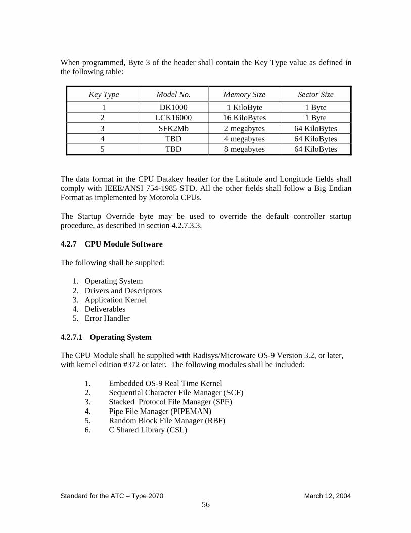
Standard for the ATC – Type 2070 March 12, 2004 56
When programmed, Byte 3 of the header shall contain the Key Type value as defined in the following table:
Key Type Model No. Memory Size Sector Size 1 DK1000 1 KiloByte 1 Byte 2 LCK16000 16 KiloBytes 1 Byte 3 SFK2Mb 2 megabytes 64 KiloBytes 4 TBD 4 megabytes 64 KiloBytes 5 TBD 8 megabytes 64 KiloBytes
The data format in the CPU Datakey header for the Latitude and Longitude fields shall comply with IEEE/ANSI 754-1985 STD. All the other fields shall follow a Big Endian Format as implemented by Motorola CPUs. The Startup Override byte may be used to override the default controller startup procedure, as described in section 4.2.7.3.3. 4.2.7 CPU Module Software The following shall be supplied:
1. Operating System 2. Drivers and Descriptors 3. Application Kernel 4. Deliverables 5. Error Handler
4.2.7.1 Operating System The CPU Module shall be supplied with Radisys/Microware OS-9 Version 3.2, or later, with kernel edition #372 or later. The following modules shall be included:
1. Embedded OS-9 Real Time Kernel 2. Sequential Character File Manager (SCF) 3. Stacked Protocol File Manager (SPF) 4. Pipe File Manager (PIPEMAN) 5. Random Block File Manager (RBF) 6. C Shared Library (CSL)

Standard for the ATC – Type 2070 March 12, 2004 57
Boot Image shall include the following utility modules:
Break Date Deiniz Devs Free Copy Dir Tmode Edt List Load Deldir Dump Del Ident Iniz Irqs Events Echo Format Dcheck Login Link Kermit Tsmon Mdir Mfree Pd Makdir Save Attr Rename Procs Unlink Sleep Xmode Shell Build Setime Merge
4.2.7.2 Drivers and Descriptors 4.2.7.2.1 Supplied modules shall be re-entrant, address independent, and shall not contain self-modifying code. Device drivers which require extensions to the standard OS-9 libraries shall use the _os_getstat() and _os_setstat() functions. A custom setstat code and parameter structure are defined as follows:
#define SS_2070 0x2070 error_code _os_getstat(path_id path, SS_2070, PB2070 *pb); error_code _os_setstat(path_id path, SS_2070, PB2070 *pb); typedef struct {
u_int32 code; u_int32 param1; union {
u_int32 param; void *pointer;
} param2; } PB2070, *pb;
The following subcodes for use with PB2070.code are also defined:
#define GS2070_Status 0x1C #define SS2070_SSig 0x1A #define SS2070_IFC 0x22 #define SS2070_OFC 0x23 #define SS2070_Timer_Sig 0x1000 #define SS2070_Timer_Cyc 0x1001
Standard for the ATC – Type 2070 March 12, 2004 58
#define SS2070_Timer_Start 0x1002 #define SS2070_Timer_Stop 0x1003 #define SS2070_Timer_Reset 0x1004
Note: When PB2070.param2.pointer is used, PB2070.param1 should be loaded with the size of what PB2070.param2.pointer is referencing. When calling _os_getstat() or _os_setstat(), all reserved or unused parameters and fields in PB2070 should be loaded with 0 (zero). 4.2.7.2.2 Drivers shall be provided to access the FLASH, SRAM, and DRAM memories. The following descriptors shall apply:
/f0 FLASH drive non-volatile, writeable /dd FLASH drive OS-9 default device for /f0 /f0wp FLASH Drive as /f0 but, write protection /f0fmt FLASH Drive as /f0 except format enabled /r0 SRAM Drive non-volatile ramdisk /r0fmt SRAM Drive as /r0 but format enabled
/r2 DRAM Drive volatile 1 MB ramdisk, not automatically initialized
4.2.7.2.3 A driver to handle each of the four internal timers under the OS-9 Kernel shall be provided. Access to the MC68360 internal timers shall be provided through the following device descriptors: 4.2.7.2.3.1 Descriptor names for each timer:
timer1 = access to MC68360's internal timer #1 timer2 = access to MC68360's internal timer #2 timer3 = access to MC68360's internal timer #3 timer4 = access to MC68360's internal timer #4 timer12 = access to MC68360's internal timer #1 & #2 (cascaded) timer34 = access to MC68360's internal timer #3 & #4 (cascaded)
4.2.7.2.3.2 Timer Standard OS-9 Function Calls: error_code _os_open (char *timer_desc_name, path_id *path);
Standard for the ATC – Type 2070 March 12, 2004 59
error_code _os_read (path_id path, void *timer_value, u_int32 *size);
Note: Prior to calling _os_read(), size must be loaded with the value 4 and timer value must be pointed to a u_int32. _os_read() shall read the current timer value and load it into timer_value as µS x 100.
error_code _os_close (path_id path); 4.2.7.2.3.3 Timer Extension to Standard OS-9 Function Calls:
error_code _os_setstat(path_id path, SS_2070, PB2070 *pb); The timer drivers shall support the following modes using the SS_2070 _os_setstat() option code and a custom parameter block structure: a) Send signal after specified time interval. Sets timer to zero and schedules
individual one-shot signal. pb→code = SS2070_Timer_Sig (0x1000); /* request for one-shot signal */ pb.param1 = signal; /* signal code to send (0 = do not send a signal and cancel
any pending signals) */” pb→param2.param = period; /* timer period in microseconds x 100 */
b) Send recurring periodic signal. Sets timer to zero and schedules repeating periodic
signal. pb→code = SS2070_Timer_Cyc (0x1001); /* request for periodic signal */ pb.param1 = signal; /* signal code to send (0 = do not send a signal and cancel
any pending signals) */” pb→param2.param = period; /* timer period in microseconds x 100 */ c) Start timer. Start the timer if stopped. Timer will free run in a periodic mode,
starting at the current timer value as its initial value and timer’s maximum allowable time as its timer period (6.5535 seconds for timers 1-4 and 429496.7295 seconds for timers 12 and 34). Timer will not send a signal and any pending signals will be cancelled. Timer mode will be SS2070_Timer_Start. pb.code = SS2070_Timer_Start (0x1002); /* start timer if stopped */”
d) Stop timer. Leaves current value in timer. Cancels any pending signals.

Standard for the ATC – Type 2070 March 12, 2004 60
pb→code = SS2070_Timer_Stop (0x1003); /* stop timer if running */ e) Reset timer. Stops timer if running, resets timer value to zero, and cancels any
pending signals. pb→code = SS2070_Timer_Reset (0x1004); /* reset timer (stop and zero) */ 4.2.7.2.3.4 Timer Extension to Standard OS-9 Function Calls: error_code _os_getstat(path_id path, SS_2070, PB2070 *pb); The timer driver will support the following function using the SS_2070 _os_getstat() option code and custom parameter block structure: a) Retrieve current timer configuration. typedef struct { u_int32 value; u_int32 mode; u_int32 signal; u_int32 period; } Timer_status; pb→code = GS2070_Status (0x1C) /* Request timer status data */ pb→param1 = sizeof(Timer_status) pb→param2.pointer = Timer_status*
Status data shall be returned in the structure pointed to by pb→param2.pointer as follows:
pb→param2.pointer→value /* current timer value in µS x 100 */
pb→param2.pointer→mode /* SS2070_Timer_Sig if one-shot signal pending, SS2070_Timer_Cyc if periodic signal pending, SS2070_Timer_Start if free running, SS2070_Timer_Stop if not active */
pb→param2.pointer→signal /* signal code pending if SS2070_Timer_Sig or SS2070_Timer_Cyc, 0 otherwise */ pb→param2.pointer→period /* timer period in microseconds x 100 if

Standard for the ATC – Type 2070 March 12, 2004 61
SS2070_Timer_Sig or SS2070_Timer_Cyc, 0 otherwise */ 4.2.7.2.3.5 All timer periods are specified in units of hundreds of microseconds, i.e. a timer period of 7 = 700 microseconds. The minimum allowed timer period shall be 500 microseconds. The maximum timer period for timers 1-4 shall be 6.5535 seconds (0xFFFF). The maximum timer period for timer12 and timer34 shall be 429496.7295 seconds (0xFFFFFFFF). The driver shall return error E$Param from _os_setstat() if the requested timer period is outside the allowable range. 4.2.7.2.4 Access and control to the CPU Datakey shall be provided through the following descriptor name and OS-9 functions: Descriptor Name
datakey = access to the CPU Datakey Function Calls
error_code _os_open (char *datakey_desc_name, path_id *path);
error_code _os_close (path_id path); error_code _os_read (path_id path, void *data_buffer, u_int32 *data_size);
error_code _os_write (path_id path, void *control, u_int32 *data_size);
error_code _os_seek(path_id path,u_int32 position); sets read / write offset error_code = _os_ss_erase(path_id path, u_int32 num_sec_erase); /*erases sector(s) if pointer is on a block boundary, returns E$PARAM error if not on a boundary */” error_code = _os_gs_pos(path_id path,u_int32 *position); /* gets current file pointer position */ error_code = _os_gs_size(path_id path, u_int32 *size); /* gets current datakey size */”
Error Codes Returned by Function Calls
E$NotRdy if datakey is not inserted

Standard for the ATC – Type 2070 March 12, 2004 62
E$Seek if Offset plus *data_size is beyond end of CPU Datakey. E$EOF if upon read or write, the last byte of CPU Datakey has previously been processed.”
Note: Use of SCF to implement the Datakey driver is not allowed. 4.2.7.2.5 The asynchronous serial communications device drivers shall support the six flow control modes (FCM#) described below: FCM# Description 0) No Flow Control Mode: The driver transmits data regardless of the state of CTS.
Upon a write command, the driver asserts RTS, and de-asserts RTS when data transmission is completed. This is the default mode. When user programs issue the first RTS related command, the driver switches to Manual Flow Control Mode (FCM# 1).
1) Manual Flow Control Mode: The driver transmits data regardless of the state of
CTS. The user program has absolute control of the RTS state. The driver doesn’t automatically assert or de-assert RTS.
2) Auto-CTS Flow Control Mode: The driver transmits data only when CTS is
externally asserted. The user program has absolute control of the RTS state. The driver doesn’t automatically assert or de-assert RTS.
3) Auto-RTS Flow Control Mode: The driver transmits data regardless of the state of
CTS. Upon a write command, the driver asserts RTS, and de-asserts RTS when data transmission is completed and any configured RTS extension is elapsed. If the user program asserts RTS, then RTS remains on until the user program de-asserts RTS. If the user program de-asserts RTS before the transmission buffer is empty, the driver holds RTS on until the transmission buffer is empty and any configured RTS extension is elapsed.
4) Fully Automatic Flow Control Mode: The driver transmits data only when CTS is
externally asserted. Upon a write command, the driver asserts RTS and waits for CTS, starts data transmission when CTS is asserted, and de-asserts RTS when data transmission is completed and any configured RTS extension is elapsed. If user program asserts RTS, then RTS remains on until the user program de-asserts RTS. If the user program de-asserts RTS before the transmission buffer is empty, the driver holds RTS on until the transmission buffer is empty and any configured RTS extension is elapsed.
5) Dynamic Flow Control Mode: The driver transmits data only when CTS is
externally asserted. The driver controls RTS based on the status of its receiving

Standard for the ATC – Type 2070 March 12, 2004 63
buffer. The driver asserts RTS continuously as long as its receiving buffer has sufficient capacity to store incoming data. If the receiving buffer approaches full, the driver de-asserts RTS until enough data has been read from the buffer to create sufficient receive capacity.
4.2.7.2.5.1 The serial device driver shall be able to set user options via _os_setstat() and return status via _os_getstat(). To support legacy application programs, the device driver shall also be able to set user options via _os_ss_size() and to return status via _os_gs_size(): error_code_os_setstat(path_id path, SS_2070, void *pb);
error_code_os_getstat(path_id path, SS_2070, void *pb); error_code_os_ss_size(path_id path, u_int32 size); error_code_os_gs_size(path_id path, u_int32 *size);
Note: The preferred method of accessing serial device drivers is through _os_setstat() and _os_getstat(). The _os_ss_size() and _os_gs_size() interface may not be required by future versions of this specification and is therefore not recommended for new development. The option subcodes to be passed in pb→code and the data to be contained in pb→param1 are defined as follows. pb→param2 is unused here and should be set to 0 (zero). For _os_ss_size() and _os_gs_size(), the size argument is the same format as pb→param1. 4.2.7.2.5.2 The supported _os_setstat() / _os_ss_size() options shall be as follows. a) Subcode passed in pb→code is SS2070_OFC (0x23).
Data passed in pb→param1 is defined as follows:
Bits Description
31-24 Auto RTS turn-off extension in number of characters (range:0-255, 0=default). 23-14 Reserved for future use.
13 Inhibit return of error E$Write from _os_write() when transmit buffer full in FCM# 2, 4, 5 (default=0, 0=error, 1=block)
12 Inhibit variable SCC MRBLR (default =0; 0=NO; 1=inhibit). 11 Inhibit SCC TODR (default=0; 0=NO; 1=inhibit). 10-8 Flow Control Mode Number (FCM#) (range:0-5). 7-0 Subcode SS2070_OFC (0x23).

Standard for the ATC – Type 2070 March 12, 2004 64
Variable MRBLR (68360 SCC) To reduce the IRQ handler overhead, the 68360 SCC driver shall use variable MRBLR as follows. If SS2070_OFC bit 12 is set to 1, the MRBLR shall be fixed at 16 for all baud rates. Variable MRBLR is not required for SP1 or SP8 on the 2070-1B CPU Module.
Baud Rate MRBLR Setting
1200 1 2400 2 4800 4 9600 8 19200 & Higher 16
TODR (68360 SCC only)
TODR requests processing a new TX buffer immediately. To reduce impact on other serial channel operations, SS2070_OFC bit 11 may be set to 1 to prevent assertion of TODR. TODR is not required for SP1 or SP8 on the 2070-1B CPU Module.
b) Subcode passed in pb→code is SS2070_IFC (0x22).
Data passed in pb→param1 is defined as follows:
Bits Description 31-11 Reserved for Future Use. 10 DCD must be asserted to receive data (default=0; 0=NO; 1=YES). 9-8 Reserved for Future Use. 7-0 Subcode = SS2070_IFC (0x22). c) Subcode passed in pb→code is SS2070_SSig (0x1A).
1. If CTS is currently negated and bits 16 – 31 are not all 0:
Setting the SS2070_SSig parameter block bit 11 (send when CTS is asserted) will cause the controller to send a one-shot signal as soon as CTS is asserted. Setting the SS2070_SSig parameter block bit 12 (send when CTS is negated) will cause the controller to send a one-shot signal immediately.
2. If CTS is currently asserted and bits 16 – 31 are not all 0: Setting the SS2070_SSig parameter block bit 11 (send when CTS is asserted) will cause the controller to send a one-shot signal immediately. Setting the SS2070_SSig parameter block bit 12 (send when CTS is negated) will cause the controller to send a signal one-shot as soon as CTS is negated.

Standard for the ATC – Type 2070 March 12, 2004 65
3. If both bits 11 and 12 of the SS2070_SSig parameter block are set, and bits 16 – 31 are not all 0: The controller will send a one-shot signal upon the next change of CTS state.
Data passed in pb→param1 is defined as follows:
Bits Description
31-16 A signal number to be sent to calling process when the state of an input changes. 15-13 Reserved for Future Use. 12 Send signal when CTS is de-asserted. 11 Send signal when CTS is asserted. 10-8 Reserved for Future Use. 7-0 Subcode = SS2070_SSig (0x1A). 4.2.7.2.5.3 The supported _os_getstat()_ / _os_gs_size() options shall be as follows. a) Subcode passed in pb→code is GS2070_Status (0x1C).
Data returned in pb→param1 is defined as follows:
Bits Description
31-16 Current unfilled transmit buffer character count of the serial device driver. 15-11 Reserved for Future Use. 10-8 Current Flow Control Mode Number (FCM#). 7 Reserved for Future Use. 6 Overrun error –0=no error; 1=error has occur since last GS2070_Status call. 5 Frame error –0=no error; 1=error has occur since last GS2070_Status call. 4 Parity error –0=no error; 1=error has occur since last GS2070_Status call. 3-2 Reserved for Future Use. 1 DCD state –0=de-asserted; 1=asserted. 0 CTS state –0=de-asserted; 1=asserted. 4.2.7.2.6 Device drivers compliant with the OS-9 SCFMAN shall be provided for CPU Activity LED Indicator and Day Light Savings time correction features. The descriptor names shall be as follows:
Standard for the ATC – Type 2070 March 12, 2004 66
led = access to CPU Activity LED Indicator dstclock = access to Daylight Savings Time Clock correction The standard OS-9 SCFMAN library calls and their functions are as follows: error_code _os_open (char *desc_name, path_id *path); //open descriptor for command error_code _os_close (path_id path); //close descriptor error_code _os_write (path_id path, void *value, u_int32 *data_size); //set value of function *value = 1, turn on LED or enable DST correction (default) *value = 0, turn off LED or disable DST correction set u_int32*data_size to 1 error_code _os_read (path_id path, void *value, u_int32 *data_size ); //get current state set u_int32*data_size to 1 4.2.7.2.7 The Manufacturer shall provide the following features to support the TOD operation and synchronization. 4.2.7.2.7.1 Leap Year and Daylight Savings Time (DST) Adjustments - The OS-9 System clock / calendar shall automatically be adjusted to account for DST and leap years. 4.2.7.2.7.2 Setting Hardware Clock from OS-9 System Clock - A device driver compatible with the OS-9 SCFMAN shall be provided to allow the hardware TOD clock/calendar to be updated from the OS-9 system clock under application control. The descriptor name shall be “ClockUpdate.” Opening the descriptor shall cause the driver to synchronize the clock to a minimum of 10 milliseconds resolution. The driver shall compensate for any time elapsed during the process of updating the hardware clock.
Standard for the ATC – Type 2070 March 12, 2004 67
4.2.7.2.7.3 Setting OS-9 System Clock from Hardware Clock - At system power up, the OS-9 system TOD clock/calendar shall automatically be updated from the hardware TOD clock. The clocks shall be synchronized to a minimum of 10 milliseconds resolution. 4.2.7.2.8 The current sector of FLASH being written shall first be backed up in SRAM. The backup sector copy shall be invalidated when FLASH write operation is completed. In case of power failure, the FLASH driver shall detect the presence of the valid backup sector copy in SRAM and shall read sector data from the valid backup sector copy. A user write operation shall restore the valid backup sector copy first. Execution of the program module, “FLRESTORE,” in the Boot Image shall also restore the valid backup sector copy to FLASH drive after a specified delay. “FLRESTORE” shall accept a delay parameter in seconds ranging from 0 to 600 seconds. The default delay factor is 30 seconds. No more that 150 KB of SRAM shall be dedicated to this purpose. Warning: Power loss or other interruption while writing to the FLASH drive may cause FLASH drive file and/or disk corruption. It is therefore strongly recommended that the FLASH drive be used to hold controller applications only. 4.2.7.2.9 Network Requirements MODEL 2070-1A and 2070-1B CPU modules shall include the following set of standard OS-9 networking modules in the operating system boot image, sufficient to support network configuration, startup, and ftp and telnet servers:
spip, ip0, sptcp, tcp0 spudp, udp0, spraw, raw0, spenet, enet, netdb (dns version), ipstart, ifconfig, route, ndbmod, ftpd, ftpdc, telnetd, telnetdc, pkman, pkdrvr, pk, pks, ping, dhcp.
The boot image shall include a default inetdb module with a module revision of zero. It shall contain the following entries only:
Hosts localhost 127.0.0.1 me
Protocols ip 0 IP icmp 1 ICMP igmp 2 IGMP tcp 6 TCP udp 17 UDP
Services ndp 13312/tcp ndpd npp 13568/tcp nppd echo 7/tcp echo 7/udp

Standard for the ATC – Type 2070 March 12, 2004 68
ftp-data 20/tcp ftp-data 20/udp ftp 21/tcp ftp 21/udp telnet 23/tcp telnet 23/udp nameserver 42/tcp nameserver 42/udp tftp 69/tcp tftp 69/udp
The boot image shall include a default inetdb2 module with a module revision of zero. It shall contain the following entry only:
Interfaces enet0 binding /spqe0/enet (no address, netmask, or broadcast)
On the MODEL 2070-1B CPU module, an OS-9 SPF Ethernet hardware driver and descriptor for the 68360 (SCC1) shall be provided in the operating system Boot Image. The descriptor shall be named spqe0. 4.2.7.2.10 Standard OS-9 File System Configuration The following set of files shall be provided on a PC-readable CD to allow a 2070 to be configured with a typical OS-9 development system file configuration. A setup utility or script shall be provided to copy the directories and files from the CD to the /f0 flash drive on a controller. 4.2.7.2.10.1 /CMDS, /CMDS/BOOTOBJS, /ETC and /SYS directories shall be used to organize the files. The contents of these directories are defined below. Execute permission shall be included in the attributes of all files in the /CMDS directory. 4.2.7.2.10.2 /SYS shall contain a default "password" file following the standard OS-9 password file format. A username “super” with password “user” shall be defined in the password file. /SYS shall also contain the following four standard OS-9 network configuration shell script files: startspf, startnfs, loadspf and loadnfs. 4.2.7.2.10.3 The utilities tar, make, fixmod, login, tsmon, and mshell shall be included in the /CMDS directory.

Standard for the ATC – Type 2070 March 12, 2004 69
4.2.7.2.10.4 The following OS-9 modules should be included in the /CMDS/BOOTOBJS directory to allow for standard TCP/IP network communications using Ethernet Protocol over Ethernet hardware and/or Serial Line Internet Protocol (SLIP) or Point-to-Point Protocol over serial links:
1. Drivers and Descriptors for PPP: spipcp, ipcp0, splcp, lpc0, sphdlc, hdlc0, hdlc1, hdlc2, hdlc3.
2. Drivers and Descriptors for SLIP: spslip, spsl0, spsl1, spsl2, spsl3. 3. LAN Comm Pak modules: spenet, enet, spip, ip0, sptcp, tcp0, spudp,
udp0, spraw, raw0, sproute, route0 4. Telnet support modules: pkman, pkdvr, pk, pks 5. Network Trap Handler: netdb_local, netdb_dns 6. NFS Modules: nfs, nfsnul and nfs_devices.
The following Network utilities shall be included in the /CMDS directory:
arp, dhcp, ftp, ftpd, ftpdc, idbdump, idbgen, rpcdbgen, ifconfig, inetd, ipstart, ndbmod, netstat, ping, route, routed, telnet, telnetd, tftpd, tftpdc, telnetdc, hostname, nfsc, mount, rpcdump, nfsstat, exportfs, portmap, pppd, chat, pppauth, nfsd, mountd, and showmount.
Default inetdb, inetdb2 and rpcdb modules shall be generated by the make utility via the use of a makefile and the network configuration files residing the /ETC directory. The generated inetdb, inetdb2 and rpcdb modules should be located in the /CMDS/BOOTOBJS directory. The modules shall be configured with the network default values as defined in Section 4.2.6 (Datakey).
A Utility Program named netcfg shall be provided. If the Datakey is present and valid, netcfg shall set the IP Address, Subnet Mask and Default Gateway of the enet0 interface when executed by a user at the command line. The netcfg utility shall also provide command line options to allow the user to write and display the network parameters in the Datakey header, write and display the Startup Override byte in the Datakey header, and copy a script or executable file from disk to the Datakey following the header. If the Datakey is not present or invalid, netcfg shall display an error and exit without altering any configuration. The netcfg utility shall reside in /CMDS. The PPP and SLIP descriptors shall have baud rates and ports set as follows and shall reside in the /CMDS/BOOTOBJS directory:
hdlc0 and spsl0 configured to use /sp1 and 38400 bits per second hdlc1 and spsl1 configured to use /sp2 and 115200 bits per second hdlc2 and spsl2 configured to use /sp3 and 115200 bits per second hdlc3 and spsl3 configured to use /sp4 and 38400 bits per second
A set of example configuration files consistent with the above networking modules shall be provided in the /ETC directory. This directory shall contain the following text files:

Standard for the ATC – Type 2070 March 12, 2004 70
hosts, hosts.equiv, networks, protocols, services, inetd.conf, resolv.conf, hosts.conf, rpc, interfaces.conf, routes.conf. makefile, nfs.map, nfsd.map
4.2.7.3 Application Kernel 4.2.7.3.1 The provided software shall boot OS-9 from SYSRESET. The entire program shall be resident in FLASH Memory. The asynchronous serial port descriptors shall be configured with the following defaults: 8-bit word, 1 stop bit, no parity, no pause, Xon and Xoff both OFF. Port SP4 shall have echo enabled, all other ports shall have no echo. Default speeds shall be as defined in Figure 4-7-7. 4.2.7.3.2 Hardware initialization, preliminary self-test, OS-9 initialization (except Extended Memory Test), and forking OPEXEC shall be completed in less than 2.0 seconds. 4.2.7.3.3 The boot image init module shall be configured with the default directory name as /f0wp and sysgo as the first executable module. Sysgo shall operate as follows:
1. Sysgo shall set the execution directory to /f0wp/CMDS 2. Sysgo shall check if the backspace key (0x08) is being received on /sp4
(c50s). If received, Sysgo shall: a. Fork a shell on /sp4 using the current directory. b. Remain an active process and monitor the shell for termination. If
the shell does terminate, Sysgo shall fork another shell on /sp4. Unless Sysgo dies, a shell shall always be provided on /sp4.
3. If the backspace key was not received, Sysgo shall check for the presence of a Datakey. If present and valid, Sysgo shall check the Startup Override byte in the Datakey header.
If Startup Override is 0x01, Sysgo shall: a. Fork a shell that executes a shell script stored on the Datakey
immediately following the header. The script must be stored as ASCII text, terminated with EOF (0x04) or 0xFF, and must not exceed 4KB in size.
b. If there is any error starting the script or if the shell terminates, Sysgo shall fork another shell as described in step 2.
If Startup Override is 0x02, Sysgo shall: a. Fork an executable module stored on the Datakey immediately
following the header. b. If there is any error forking the module or if the module terminates,
Sysgo shall fork a shell as described in step 2.

Standard for the ATC – Type 2070 March 12, 2004 71
4. If the backspace key was not received and Startup Override was not performed: a. Sysgo shall fork the module named /f0wp/OPEXEC if present at
/f0wp. b. If there is any error forking OPEXEC, Sysgo shall fork a shell as
described in step 2. If there are no errors forking OPEXEC, Sysgo shall then exit without forking a shell.
5. If the backspace key was not received, Startup Override was not performed, and there is no OPEXEC file: a. Sysgo shall fork a shell that executes a shell script named
/f0wp/startup if present at /f0wp. b. If there is any error starting the script or if the shell terminates,
Sysgo shall fork another shell as described in step 2. 6. If the backspace key was not received, Startup Override was not
performed, and there is no OPEXEC and no startup file: a. Sysgo shall fork a shell as described in step 2.
The backspace command applies to the current line, regardless of auto-wrap or auto-scroll. 4.2.7.3.4 A Short Out is defined as the period of time between ACFAIL/POWER DOWN transition to LOW and back to HIGH without a SYSRESET transition to LOW. ACFAIL/POWER DOWN transitions shall generate an interrupt. The interrupt shall update an OS-9 event named "ACFAIL". The "ACFAIL" event shall set a value 1 indicating an ACFAIL condition occurred for the DOWN transition and set 0 indicating non-ACFAIL condition for the HIGH transition. The IRQ7 and auto-vector 31(7) shall not be used to update the "ACFAIL" event. In addition, the ACFAIL condition shall generate the OS-9 auto-vector 30(6) interrupt service. Each interrupt service installed shall exit with the "Carry Bit" set allow OS9 to propagate the ACFAIL interrupt. The Manufacturer shall supply an interrupt handler at priority 255 that acknowledges and clears the interrupt. Priority 1 shall be reserved for the OS-9 system. 4.2.7.3.5 A Long Out is defined as ACFAIL transition to LOW follow by a SYSRESET going LOW. The SYSRESET going HIGH shall be followed by an operating system reboot.
Standard for the ATC – Type 2070 March 12, 2004 72
4.2.7.4 Error Handler 4.2.7.4.1 A Manufacturer may include an error handling routine to save troubleshooting data regarding initialization, power-up test abnormalities and other error conditions. If used, the error report shall be stored in the file /r0/ErrorReport and shall not exceed 11 kilobytes in size. 4.2.7.5 Diagnostic Acceptance Test (DAT) 4.2.7.5.1 When required, a DAT Program shall be provided resident in the Type 2070 ATC Unit as the application program. 4.2.7.5.2 Deleted 4.2.7.6 Re-Flash Utility A Utility Program shall be provided that would allow the user to upgrade (re-flash) the Boot Image as defined in section 4.2.7. This utility shall provide the capabilities for upgrading the Operating System and drivers when available by the manufacturer. The Utility Program shall provide the capability for the user to dynamically upgrade the Boot Image via the command prompt. The Manufacturer shall also provide a copy in CD Memory of all files originally stored in the flash drive /f0 so that they can be reloaded as needed. 4.2.7.7 Deliverables 4.2.7.7.1 The following items will be provided to the purchasing AGENCY on a CD disk readable by a PC compatible computer.
1. Specific hardware memory addresses, including FLASH, SRAM, and DRAM starting addresses, shall be specified and provided. Written documentation of addresses shall be in PDF form and will have the file name of “Memory Map.pdf”
2. Copy of all provided written manuals in PDF form. 3. RE-FLASH Utility and the procedures for its use in PDF form. The PDF
documentation of the procedures shall have the file name of “Reflash Utility Procedures.pdf”.

Standard for the ATC – Type 2070 March 12, 2004 73
4.2.7.7.2 If the agency feels that knowledge of the source code and/or access to the source code is necessary for the purchase of Type 2070 ATC’s, then they are referred to forthcoming guidance documents for provisions which should be included in a procurement specification to protect the interests of both the Manufacturer and the Agency. 4.2.7.7.3 OS-9 compliant header files shall be provided with all driver modules. 4.3 Type 2070-2 Field I/O Module (FI/O) 4.3.1 Type 2070-2A Module The TYPE 2070-2A MODULE shall consist of the Field Controller Unit; Parallel Input/Output Ports; other Module Circuit Functions (includes muzzle switch); Serial Communication Circuitry; Module Connectors C1S, C11S, and C12S mounted on the module front plate; VDC Power Supply (+12VDC to +5VDC); and required resident software. 4.3.2 Type 2070-2B Module The TYPE 2070-2B MODULE shall consist of the Serial Communication Circuitry, VDC Power Supply, and Module Connector C12S mounted on the module front plate only. 4.3.3 Field Controller Unit (FCU) The FCU shall include a programmable microprocessor/controller unit together with all required clocking and support circuitry. Operational software necessary to meet housekeeping and functional requirements shall be provided resident in socketed firmware. 4.3.4 Parallel I/O Ports 4.3.4.1 The I/O Ports shall provide 64 bits of input using ground-true logic. Each input shall be read logic "1" when the input voltage at its field connector input is less than 3.5 VDC, and shall be read logic "0" when either the input current is less than 100 microamperes or the input voltage exceeds 8.5 VDC. Each input shall have an internal pull-up to the Isolated +12 VDC and shall not deliver greater than 20 milliamperes to a short circuit to ground.

Standard for the ATC – Type 2070 March 12, 2004 74
4.3.4.2 The I/O Ports shall provide 64 bits of output. Inputs shall have the following characteristics:
1. A voltage between 0 and 4 volts shall be considered the Low (True/Operate) state.
2. A voltage greater than 8 volts shall be considered the High (False) state. 3. The transition from the Low state to High state (and vice versa) shall
occur between 4 and 8 volts. Outputs shall have the following characteristics:
1. The Low (True/Operate) voltage shall be between 0 and 3 volts. 2. Current sinking capability in the Low state shall be at least 100
milliamperes. 3. With an external impedance of 100 kiloOhms or greater, the transition
from 4 to 16 volts (and vice versa) shall be accomplished within 0.1 millisecond.
4. The High state impedance shall exceed 1 Megohms to 12 volts DC. 4.3.4.3 Each output shall latch the data written and remain stable until either new data is written or the active-low reset signal. Upon an active-low reset signal, each output shall latch a logic "0" and retain that state until a new writing. The state of all output circuits at the time of Power Up or in Power Down state shall be open (logic 0). It shall be possible to simultaneously assert all outputs within 100 microseconds of each other. An output circuit state not changed during a new writing shall not glitch when other output circuits are updated. 4.3.5 Other Module Circuit Functions 4.3.5.1 A maximum capacitive load of 100 picofarads shall be presented to the LINESYNC input signal. The EIA-485 compliant differential LINESYNC signals shall be derived from the LINESYNC signal. 4.3.5.2 An External WDT “Muzzle” Jumper shall be provided on the board. With the jumper in and NRESET transitions HIGH (FCU active), the FCU shall output a state change on Output Port 5, bit 8 (Connector C1, pin 103 – Monitor Watchdog Timer Input) every 100 milliseconds for 10 seconds or due to CPU Command. When the jumper is missing (open), the feature shall not apply. This feature is required to operate with the Type 210 Monitor Unit only.

Standard for the ATC – Type 2070 March 12, 2004 75
4.3.5.3 A WATCHDOG Circuit shall be provided. It shall be enabled by the FIELD I/O software at Power Up with a value of 100 milliseconds. Its enabled state shall be machine readable and reported in the FI/O status byte. Once enabled, the watchdog timer shall not be disabled without resetting the FI/O. Failure of the FI/O to reset the watchdog timer within the prescribed timeout shall result in a hardware reset. 4.3.5.4 One KHz Reference A synchronizable 1 kilohertz time reference shall be provided. It shall maintain a frequency accuracy of +/-0.01% (+/-0.1 counts per second). 4.3.5.5 A 32-bit MILLISECOND COUNTER (MC) shall be provided for “timestamping.” Each 1 KHz reference interrupt shall increment the MC. 4.3.5.6 At Power Up, the FCU loss of communications timer shall indicate loss of communications until the user program sends the Request Module Status message to reset the “E” Bit and a subsequent set output command is processed. 4.3.5.7 A LOGIC Switch shall be provided resident on the module board. The switch shall function to disconnect Serial Port 3 (SP3) from the external world, Connector C12S. Its purpose is to prevent multiple use of SP3. A LED shall be provided on the module front panel labeled “SP3 ON”. If LED light ON, SP3 is active and available at C12S. 4.3.6 Serial Communications/Logic Circuitry 4.3.6.1 System Serial Port 5 (SP5) EIA-485 signal lines shall enter the I/O Module and be split into two multi-drop isolated ports. One shall be routed to the FCU and the other converted to EIA-485, then routed to Connector C12S. 4.3.6.2 System Serial Port 3 (SP3) EIA-485 signal lines shall enter the I/O module and be isolated, converted back to EIA-485 and then routed to connector C12S.
Standard for the ATC – Type 2070 March 12, 2004 76
4.3.6.3 LINE SYNC and POWER DOWN lines shall be split and isolated, one routed to the FCU for shut down functions and the other changed to EIA-485; then routed to connector C12S for external module use. 4.3.6.4 CPU RESET and POWER UP (SYSRESET) lines shall be isolated and “OR’d” to form NRESET. NRESET shall be used to reset FCU and other module devices. NRESET shall also be converted to EIA-485 then routed to connector C12S. 4.3.6.5 If the Type 2070 module is a –2B, then routing to FCU doesn’t apply. 4.3.6.6 Isolation is between internal +5 VDC / Ground #1 and +12 VDC ISO / VDC Ground #2. +12 VDC ISO is for board power and external logic. 4.3.7 Buffers A Transition Buffer shall be provided capable of holding a minimum of 1024 recorded entries. The Transition Buffer shall default to empty. There shall be two entry types: Transition and Rollover. The inputs shall be monitored for state transition. At each transition ( If the input has been configured to report transition), a transition entry shall be added to the Transition Buffer. The MC shall be monitored for rollover. At each rollover transition ($xxxx FFFF - $xxxx 0000), a rollover entry shall be added to the Transition Buffer. For rollover entries, all bits of byte 1 are set to indicate that this is a rollover entry. Transition Buffer blocks are sent to the CPU module upon command. Upon confirmation of their reception, the blocks shall be removed from the Transition Buffer. The entry types are depicted as follows: Input Transition Entry
Description msb lsb Byte Number
Transition Entry Identifier S Input Number 1 MC Timestamp NLSB x x x x x x x x 2 MC Timestamp LSB x x x x x x x x 3 Millisecond Counter Rollover Entry
Description msb lsb Byte Number Rollover Entry Identifier 1 1 1 1 1 1 1 1 1 MC Timestamp MSB x x x x x x x x 2
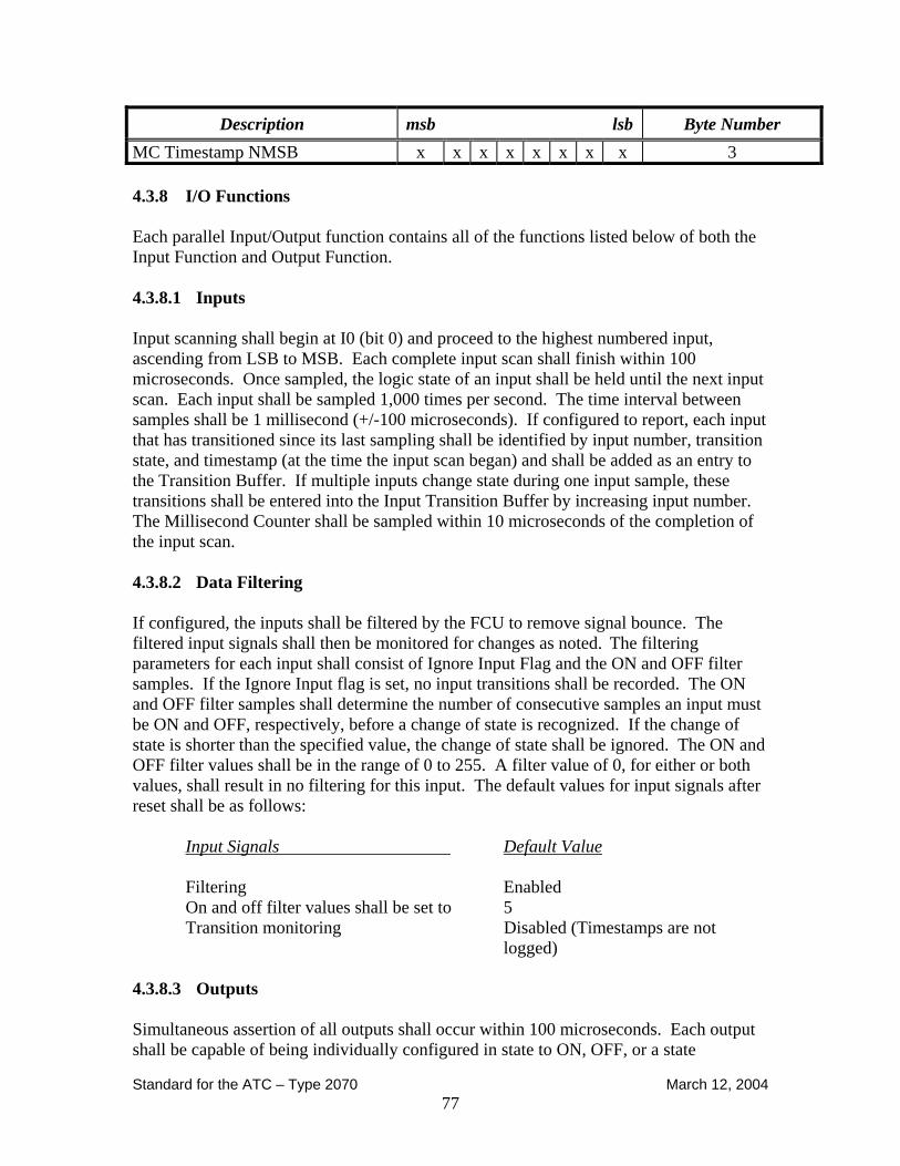
Standard for the ATC – Type 2070 March 12, 2004 77
Description msb lsb Byte Number MC Timestamp NMSB x x x x x x x x 3 4.3.8 I/O Functions Each parallel Input/Output function contains all of the functions listed below of both the Input Function and Output Function. 4.3.8.1 Inputs Input scanning shall begin at I0 (bit 0) and proceed to the highest numbered input, ascending from LSB to MSB. Each complete input scan shall finish within 100 microseconds. Once sampled, the logic state of an input shall be held until the next input scan. Each input shall be sampled 1,000 times per second. The time interval between samples shall be 1 millisecond (+/-100 microseconds). If configured to report, each input that has transitioned since its last sampling shall be identified by input number, transition state, and timestamp (at the time the input scan began) and shall be added as an entry to the Transition Buffer. If multiple inputs change state during one input sample, these transitions shall be entered into the Input Transition Buffer by increasing input number. The Millisecond Counter shall be sampled within 10 microseconds of the completion of the input scan. 4.3.8.2 Data Filtering If configured, the inputs shall be filtered by the FCU to remove signal bounce. The filtered input signals shall then be monitored for changes as noted. The filtering parameters for each input shall consist of Ignore Input Flag and the ON and OFF filter samples. If the Ignore Input flag is set, no input transitions shall be recorded. The ON and OFF filter samples shall determine the number of consecutive samples an input must be ON and OFF, respectively, before a change of state is recognized. If the change of state is shorter than the specified value, the change of state shall be ignored. The ON and OFF filter values shall be in the range of 0 to 255. A filter value of 0, for either or both values, shall result in no filtering for this input. The default values for input signals after reset shall be as follows: Input Signals Default Value Filtering Enabled On and off filter values shall be set to 5
Transition monitoring Disabled (Timestamps are not logged)
4.3.8.3 Outputs Simultaneous assertion of all outputs shall occur within 100 microseconds. Each output shall be capable of being individually configured in state to ON, OFF, or a state

Standard for the ATC – Type 2070 March 12, 2004 78
synchronized with either phase of LINESYNC. The condition of the outputs shall only be "ON" if the FI/O continues to receive active communications from the CPU Module. If there is no valid communications with the CPU Module for 2.0 seconds, all outputs shall revert to the OFF condition, and the FI/O status byte shall be updated to reflect the loss of communication from the CPU Module. The data and control bits in the CPU Module-FI/O frame protocol shall control each output as follows: Output Bit Translation
Case
Output Data Bit
Output Control
Bit
Function
A 0 0 Output in the OFF state
B 1 1 Output is a square wave, synchronized to the LINESYNC signal. When LINESYNC is ON (1), the output is OFF, and when LINESYNC is OFF (0), the output is ON.
C 0 1 Output is a square wave, synchronized to the LINESYNC signal. When LINESYNC is ON (1), the output is ON, and when LINESYNC is OFF (0), the output is OFF
D 1 0 Output is in the ON state. In Case A above, the corresponding output shall be turned OFF if previously ON and if previously OFF remain OFF until otherwise configured. For half-cycle switching (cases B and C), all outputs to be changed shall be changed within 50 microseconds after the corresponding LINESYNC transition and shall remain in the same state during the entire half cycle. In Case D above, the corresponding output shall be turned ON if previously OFF and if previously ON remain ON until otherwise configured. All outputs shall never change state unless configured to do so. 4.3.8.4 Interrupts All interrupts shall be capable of asynchronous operation with respect to all processing and all other interrupts. MILLISECOND Interrupt shall be activated by the 1 kilohertz reference once per milliseconds. An MC timestamp rollover flag set by MC rollover shall be cleared only on command. LINESYNC Interrupt - This interrupt shall be generated by both the 0-1 and 1-0 transitions of the LINESYNC signal. The LINESYNC interrupt shall monitor the MC interrupt and set the MC error flag if there has not been an interrupt from the 1 kilohertz source for 0.5 seconds (>/=60 consecutive LINESYNC interrupts). The LINESYNC interrupt shall synchronize the 1 kilohertz time reference with the 0-1 transition of the LINESYNC signal once a second. A LINESYNC error flag shall be set if the LINESYNC interrupt has not successfully executed for 0.5 seconds or longer (>/=500 consecutive millisecond interrupts).
Standard for the ATC – Type 2070 March 12, 2004 79
4.3.8.5 Communication Service Routine A low-level communication service routine shall be provided to handle reception, transmission, and EIA-485 communication faults. The communication server shall automatically: For Transmission
Generate the opening and closing flags Generate the CRC value Generate the abort sequence (minimum of 8 consecutive '1' bits) when
commanded by the FCU Provide zero bit insertion
For Receiving
Detect the opening and closing flags Provide address comparison, generating an interrupt for messages addressed to
the I/O Module, and ignoring messages not addressed to the I/O Module Strip out inserted zeros Calculate the CRC value, compare it to the received value, and generate an
interrupt on an error Generate an interrupt if an abort sequence is received
4.3.8.6 Communication Processing The task shall be to process the command messages received from the CPU Module, prepare, and start response transmission. The response message transmission shall begin within 4 milliseconds of the receipt of the received message. The time from the receipt of message to the completion of the commanded task shall not exceed 70 milliseconds. 4.3.8.7 Input Processing This task shall process the raw input data scanned in by the 1 ms interrupt routine, perform all filtering, and maintain the transition queue entries. 4.3.9 Data Communications Protocols Protocols - All communication with the CPU Module shall be SDLC-compatible command-response protocol, support 0 bit stuffing, and operate at a data rate of 614.4 kilobits per second. The CPU Module shall always initiate the communication and should the command frame be incomplete or in error, no FI/O response shall be transmitted. The amount of bytes of a command or response is dependent upon the I/O Module identification.

Standard for the ATC – Type 2070 March 12, 2004 80
4.3.9.1.1 The frame type shall be determined by the value of the first byte of the message. The command frames type values 112-127 and associated response frame type values 240-255 are allocated to the manufacturer diagnostics. All other frame types not called out are reserved. The command-response Frame Type values and message times shall be as follows: Frame Types
Module Command
I/0 Module
Response Description Minimum
Message Time Maximum
Message Time
0-43 128-171 Reserved for NEMA TS-2 49 177 Request Module Status 250 microseconds 275 microseconds
50 178 MILLISECOND CTR. Mgmt. 222.5 microseconds 237.5 microseconds
51 179 Configure Inputs 344.5 microseconds 6.8750 milliseconds52 180 Poll Raw Input Data 317.5 microseconds 320 microseconds 53 181 Poll Filtered Input Data 317.5 microseconds 320 microseconds 54 182 Poll Input Transition Buffer 300 microseconds 10.25 microseconds55 183 Command Outputs 405 microseconds 410 microseconds 56 184 Reserved 340 microseconds 10.25 milliseconds 57 185 Reserved 340 microseconds 6.875 milliseconds 58 186 Configure Watchdog 222.5 microseconds 222.5 microseconds59 187 Controller Identification 222.5 microseconds 222.5 microseconds60 188 I/O Module Identification 222.5 microseconds 222.5 microseconds
61-62 189-190 Reserved (note below) --- ---
63 191 Poll variable length raw input 317.5 microseconds 320 microseconds
64 192 Variable length command outputs 405 microseconds 410 microseconds
65 193 Reserved (note below) --- --- 67 195 Reserved (note below) --- ---
4.3.9.1.2 Messages 61 / 189, 62 / 190, 65 / 193, and 67 / 195 are reserved for ITS Cabinet Frame Types. Message 63 / Message 191 shall be the same as Message 52 / 180 except Byte 2 of Message 180 response shall denote the following number of input data bytes. Message 64 / 192 shall be the same as Message 55 / 183 except Byte 2 of the Message 55 Command shall denote the number of output data bytes, plus the following output control bytes.

Standard for the ATC – Type 2070 March 12, 2004 81
4.3.9.2 Request Module Status The Command shall be used to request FI/O status information response. Command/response frames are as follows: Request Module Status Command
Description msb lsb Byte Number (Type Number = 49) 0 0 1 1 0 0 0 1 Byte 1 Reset Status Bits P E K R T M L W Byte 2 Request Module Status Response
Description msb lsb Byte Number (Type Number = 177) 1 0 1 1 0 0 0 1 Byte 1 System Status P E K R T M L W Byte 2 SCC Receive Error Count Receive Error Count Byte 3 SCC Transmit Error Count Transmit Error Count Byte 4 MC Timestamp MSB MC Timestamp MSB Byte 5 MC Timestamp NMSB MC Timestamp NMSB Byte 6 MC Timestamp NLSB MC Timestamp NLSB Byte 7 MC Timestamp LSB MC Timestamp LSB Byte 8 4.3.9.2.1 The response status bits are defined as follows: P - Indicates FI/O hardware reset E - Indicates a communications loss of greater than 2 seconds K - Indicates the Datakey has failed or is not present R - Indicates that the EIA-485 receive error count byte has rolled over T - Indicates that the EIA-485 transmit error count byte has rolled over M - Indicates an error with the MC interrupt L - Indicates an error in the LINESYNC W - Indicates that the FI/O has been reset by the Watchdog 4.3.9.2.2 The FI/O status byte shall be updated (set to '1') to reflect the faults noted in clause 4.3.9.2.1. Each status bit shall only be reset (set to '0') when the corresponding bit of the Request Module Status Command is a '1'. The Request Module Status Response shall report the current status (subsequent to reset and sampling).

Standard for the ATC – Type 2070 March 12, 2004 82
4.3.9.2.3 The FI/O shall count the number of errored frames the FI/O Communications Processor reports. Separate counts shall be maintained for transmit and received frames. When an individual count rolls over (255-0), the corresponding roll-over flag shall be set. 4.3.9.2.4 FI/O modules with Datakey: On NRESET transition to High or immediately prior to any interrogation of the Datakey, the FI/O shall test the presence of the Key. If absent, Status Bit “K” shall be set to '1' and no interrogation shall take place. If an error occurs during the interrogation, Status Bit “K” shall be set to '1'. FI/O modules without Datakey: Status Bit "K" shall always be set to '1' 4.3.9.2.5 The MC timestamp value shall be sampled just prior to the Request Module Status Response. 4.3.9.3 MC Management MC MANAGEMENT frame shall be used to set the value of the MC. The 'S' bit shall return status '0' on completion. The 32-bit value shall be loaded into the MC at the next 0-1 transition of the LINESYNC signal. The frames are as follows: Millisecond Counter Management Command
Description msb lsb Byte Number (Type Number = 50) 0 0 1 1 0 0 1 0 Byte 1 New MC Timestamp MSB x x x x x x x x Byte 2 New MC Timestamp NMSB x x x x x x x x Byte 3 New MC Timestamp NLSB x x x x x x x x Byte 4 New MC Timestamp LSB x x x x x x x x Byte 5 Millisecond Counter Management Response
Description msb lsb Byte Number (Type Number = 178) 1 0 1 1 0 0 1 0 Byte 1 Status 0 0 0 0 0 0 0 S Byte 2 4.3.9.4 Configure Inputs The Configure Inputs command frame shall be used to change input configurations. The command-response frames are as follows:

Standard for the ATC – Type 2070 March 12, 2004 83
Configure Inputs Command
Description msb lsb Byte Number (Type Number = 51) 0 0 1 1 0 0 1 1 Byte 1 Number of Items (n) n n n n n n n n Byte 2 Item # - Byte 1 E Input Number Byte 3(I-1)+3 Item # - Byte 2 Leading edge filter (e) Byte 3(I-1)+4 Item # - Byte 3 Trailing edge filter (r) Byte 3(I-1)+5 Configure Inputs Response
Description msb lsb Byte Number (Type Number = 179) 1 0 1 1 0 0 1 1 Byte 1 Status 0 0 0 0 0 0 0 S Byte 2 Block field definitions shall be as follows:
E - Ignore Input Flag. "1" = do not report transitions for this input, "0" = report transitions for this input
e - A one-byte leading edge filter specifying the number of consecutive input samples which must be "0" before the input is considered to have entered to "0" state from "1" state (range 1 to 255, 0 = disabled)
r - A one-byte trailing edge filter specifying the number of consecutive input samples which must be "1" before the input is considered to have entered to "1" state from "0" state (range 1 to 255, 0 = disabled)
S - return status S = '0' on completion or '1' on input error out of range 4.3.9.5 Poll Raw Input Data The Poll Raw Input Data frame shall be used to poll the FI/O for the current unfiltered status of all inputs. The response frame shall contain 8 bytes (2A) or 15 bytes (2B) of information indicating the current input status. The frames are as follows: Poll Raw Input Data Command
Description msb lsb Byte Number
(Type Number = 52) 0 0 1 1 0 1 0 0 Byte 1 Poll Raw Input Data Response (2070-2A)
Description msb lsb Byte Number
(Type Number = 180) 1 0 1 1 0 1 0 0 Byte 1 Inputs I0 (lsb) to I7 (msb) x x x x x x x x Byte 2 Inputs I8 to I63 x x x x x x x x Bytes 3 to 9
Standard for the ATC – Type 2070 March 12, 2004 84
Description msb lsb Byte Number
MC Timestamp MSB x x x x x x x x Byte 10 MC Timestamp NMSB x x x x x x x x Byte 11 MC Timestamp NLSB x x x x x x x x Byte 12 MC Timestamp LSB x x x x x x x x Byte 13 Poll Raw Input Data Response (2070-8)
Description msb lsb Byte Number
(Type Number = 180) 1 0 1 1 0 1 0 0 Byte 1 Inputs I0 (lsb) to I7 (msb) x x x x x x x x Byte 2 Inputs I8 to I119 x x x x x x x x Bytes 3 to 16 MC Timestamp MSB x x x x x x x x Byte 17 MC Timestamp NMSB x x x x x x x x Byte 18 MC Timestamp NLSB x x x x x x x x Byte 19 MC Timestamp LSB x x x x x x x x Byte 20 4.3.9.6 Poll Filtered Input Data The Poll Filtered Input Data frame shall be used to poll the FI/O for the current filtered status of all inputs. The response frame shall contain 8 bytes (2A) or 15 bytes (2B) of information indicating the current filtered status of the inputs. Raw input data shall be provided in the response for inputs that are not configured for filtering. The frames are as follows: Poll Filter Input Data Command
Description msb lsb Byte Number (Type Number = 53) 0 0 1 1 0 1 0 1 Byte 1 Poll Filter Input Data Response (2070-2A)
Description msb lsb Byte Number
(Type Number = 180) 1 0 1 1 0 1 0 0 Byte 1 Inputs I0 (lsb) to I7 (msb) x x x x x x x x Byte 2 Inputs I8 to I63 x x x x x x x x Bytes 3 to 9 MC Timestamp MSB x x x x x x x x Byte 10 MC Timestamp NMSB x x x x x x x x Byte 11 MC Timestamp NLSB x x x x x x x x Byte 12 MC Timestamp LSB x x x x x x x x Byte 13 Poll Filter Input Data Response (2070-8)
Description msb lsb Byte Number (Type Number = 181) 1 0 1 1 0 1 0 1 Byte 1

Standard for the ATC – Type 2070 March 12, 2004 85
Description msb lsb Byte Number Inputs I0 (lsb) to I7 (msb) x x x x x x x x Byte 2 Inputs I8 to I119 x x x x x x x x Bytes 3 to 16 MC Timestamp MSB x x x x x x x x Byte 17 MC Timestamp NMSB x x x x x x x x Byte 18 MC Timestamp NLSB x x x x x x x x Byte 19 MC Timestamp LSB x x x x x x x x Byte 20 4.3.9.7 Poll Input Transition Buffer The Poll Input Transition Buffer frame shall poll the FI/O for the contents of the input transition buffer. The response frame shall include a three-byte information field for each of the input changes that have occurred since the last interrogation. The frames are as follows: Poll Input Transition Buffer Command
Description msb lsb Byte Number (Type Number = 54) 0 0 1 1 0 1 1 0 Byte 1 Block Number x x x x x x x x Byte 2 Poll Input Transition Buffer Response
Description msb lsb Byte Number
(Type Number = 182) 1 0 1 1 0 1 1 0 Byte 1 Block Number x x x x x x x x Byte 2 Number of Entries x x x x x x x x Byte 3 Item # S Input Number Byte 3(I-1)+4 Item # MC Timestamp NLSB x x x x x x x x Byte 3(I-1)+5 Item # MC Timestamp LSB x x x x x x x x Byte 3(I-1)+6 Status 0 0 0 0 C F E G Byte 3(I-1)+7 MC Timestamp MSB x x x x x x x x Byte 3(I-1)+8 MC Timestamp NMSB x x x x x x x x Byte 3(I-1)+9 MC Timestamp NLSB x x x x x x x x Byte 3(I-1)+10 MC Timestamp LSB x x x x x x x x Byte 3(I-1)+11 4.3.9.7.1 Each detected state transition for each active input (see configuration data) is placed in the queue as it occurs. The FI/O shall set the 'F' bit to '1' when attempting to record a transition and the Transition Buffer is full. While the Transition Buffer is full, all subsequent entries shall be discarded. Bit definitions are as follows:
S - Indicates the state of the input after the transition C - Indicates the 255 transition entries limit has been exceeded
Standard for the ATC – Type 2070 March 12, 2004 86
F - Indicates the transition buffer limit has been exceeded G - Indicates the requested block number is out of monotonic
increment sequence E - Same block number requested, E is set in response
4.3.9.7.2 The Block Number byte is a monotonically increasing number incremented after each command issued by the CPU Module. When the FI/O Module receives this command, it shall compare the associated Block Number with the Block Number of the previously received command. If it is the same, the previous buffer shall be re-sent to the CPU Module and the 'E' flag set in the status response frame. If it is not equal to the previous Block Number, the old buffer shall be purged and the next block of data sent. If the block number is not incremented by one, the status G bit shall be set. The block number received becomes the current number (even if out of sequence). The Block Number byte sent in the response block shall be the same as that received in the command block. Counter rollover shall be considered as a normal increment. 4.3.9.7.3 The Timestamp shall equal the MC value at the time the Poll Input Transition Buffer Response is generated. 4.3.9.8 Set Outputs The Set Outputs frame shall be used to command the FI/O to set the Outputs according to the data in the frame. If there is any error configuring the outputs, the 'E' flag in the response frame shall be set to '1'. If the LINESYNC reference has been lost, the 'L' bit in the response frame shall be set. Loss of LINESYNC reference shall also be indicated in system status information. The output bytes depend upon field I/O module. These command and response frames are as follows: Set Outputs Command
Description msb lsb Byte Number (Type Number = 55) 0 0 1 1 0 1 1 1 Byte 1 Outputs O0 (lsb) to O7 (msb) Data x x x x x x x x Byte 2 Outputs O8 to O103 Data x x x x x x x x Bytes 3 to 14 Outputs O0 (lsb) to O7 (msb) Control x x x x x x x x Byte 15 Outputs O8 to O103 Control x x x x x x x x Bytes 16 to 27 Set Outputs Response
Description msb lsb Byte Number (Type Number = 183) 1 0 1 1 0 1 1 1 Byte 1 Status 0 0 0 0 0 0 L E Byte 2

Standard for the ATC – Type 2070 March 12, 2004 87
4.3.9.9 Configure Input Tracking Functions Deleted 4.3.9.10 Configure Complex Output Functions Deleted 4.3.9.11 Configure Watchdog The Configure Watchdog frames shall be used to change the software watchdog timeout value. The Command and response frames are as follows: Configure Watchdog Command
Description msb lsb Byte Number (Type Number = 58) 0 0 1 1 1 0 1 0 Byte 1 Timeout Value x x x x x x x x Byte 2 Configure Watchdog Response
Description msb lsb Byte Number (Type Number = 186) 1 0 1 1 1 0 1 0 Byte 1 Status 0 0 0 0 0 0 0 Y Byte 2 4.3.9.11.1 The timeout value shall be in the range between 10 to 100 milliseconds. If the value is lower than 10, 10 shall be assumed. If the value is greater than 100, 100 shall be assumed. 4.3.9.11.2 On receipt of this frame, the watchdog timeout value shall be changed to the value in the message and the “Y” bit set. The response frame bit (Y) shall indicate a '1' if the watchdog has been previously set and a '0' if not. 4.3.9.12 Controller Identification This is a legacy message command / response for FI/O modules with Datakey resident. Upon command, a response frame containing the 128 bytes of the Datakey See previous sections on Request Module Status for FI/O Status Bit ‘K’ definition. If “K” bit set, only the first two bytes shall be returned. The Command and Response frames are as follows:

Standard for the ATC – Type 2070 March 12, 2004 88
Controller Identification Command Description msb lsb Byte Number
(Type Number= 59) 0 0 1 1 1 0 1 1 Byte 1 Controller Identification Response
Description msb lsb Byte Number (Type Number = 187) 1 0 1 1 1 0 1 1 Byte 1 Status 0 0 0 0 0 0 0 K Byte 2 Datakey x x x x x x x x Bytes 3 to 130 4.3.9.13 Module Identification The I/O Module Identification Command frame shall be used to request the FI/O Identification value. A response of "1" shall be returned by 2070-2A, "2" by 2070-8, "3" is reserved for NEMA TS 2 Type 1 FI/O and "32 to 40" are reserved for ITS Cabinets. The command and response frames are shown as follows: I/O Module Identification Command
Description msb lsb Byte Number (Type Number = 60) 0 0 1 1 1 1 0 0 Byte 1 I/O Module Identification Response
Description msb lsb Byte Number (Type Number = 188) 1 0 1 1 1 1 0 0 Byte 1 FI/O I D byte x x x x x x x x Byte 2 4.4 Type 2070-3 Front Panel Assembly 4.4.1 General The Type 2070-3 Front Panel Assembly (FPA) shall be delivered with one of the three options as defined in this clause. All options shall consist of a panel with Latch assembly and two TSD #1 hinge attaching devices, assembly PCB, external serial port connector(s), CPU active LED indicator, and FP Harness Interface. The options shall include the additional features, as follows:
Option 3A - FPA controller, two keyboards, AUX switch, alarm bell and Display A
Option 3B - FPA controller, two keyboards, AUX switch, alarm bell and Display B
Option 3C - System Serial Port 6 Lines, isolated and vectored to Connector C60S.

Standard for the ATC – Type 2070 March 12, 2004 89
4.4.2 Keyboards Two KEYBOARDS shall be provided, one with sixteen keys for hexadecimal alphanumeric entry and the other with twelve keys to be used for cursor control and action symbol entry. Each key shall be engraved or embossed with its function character. Each key shall have an actuation force between 50 and 100 grams and provide a positive tactile indication of contact closure. Key contacts shall be hermetically sealed, have a design life of over one million operations, shall be rated for the current and voltage levels used, and shall stabilize within 5 milliseconds following contact closure. 4.4.3 CPU Active Indicator The cathode of the CPU ACTIVE LED INDICATOR shall be electrically connected to the CPU Activity LED signal and shall be pulled up to +5 VDC. 4.4.4 Display The DISPLAY shall consist of a Liquid Crystal Display (LCD), a backlight, and a contrast potentiometer control. Display A shall have 4 lines of 40 characters each with a minimum character dimensions of 0.20 inches wide by 0.41 inches high and an electro -luminescent (EL) backlight. Display B shall have 8 lines of 40 characters each with minimum dimensions of 0.10 inches wide by 0.17 high and either LED or EL backlight. 4.4.4.1 Each character shall be composed of a 5 x 7 dot matrix with a underline row or a 5 x 8 dot matrix. The viewing angle of the LCD shall be optimized for direct (90 degrees) viewing, +/-35 degrees vertical, +/-45 degrees horizontal. The LCD shall have variable contrast with a minimum ratio of 4:1. The LCD shall be capable of displaying, at any position on the Display, any of the standard ASCII characters as well as user-defined characters. 4.4.4.2 The backlight shall be turned on and off by the Controller Circuitry. The backlight and associated circuitry shall consume no power when in off state. A potentiometer shall control the LCD contrast with clockwise rotation increasing contrast. The contrast shall depend on the angular position of the potentiometer, which shall provide the entire contrast range of the LCD. 4.4.4.3 Cursor display shall be turned ON and OFF by command. When ON, the cursor shall be displayed at the current cursor position. When OFF, no cursor shall be displayed. All other cursor functions (positioning, etc.) shall remain in effect.

Standard for the ATC – Type 2070 March 12, 2004 90
4.4.5 FPA Controller The FPA CONTROLLER shall function as the Front Panel Device controller interfacing with the CPU Module. 4.4.5.1 A FPA RESET Switch shall be provided on the Assembly PCB. The momentary CONTROL switch shall be logic OR'd with the CPU RESET Line, producing a FPA RESET Output. Upon FPA RESET being active or receipt of a valid Soft Reset display command, the following shall occur:
1. Auto-repeat, blinking, auto-wrap, and auto-scroll shall be set to OFF. 2. Each special character shall be set to ASCII SPC (space). 3. The tab stops shall be set to columns 9, 17, 25, and 33. 4. The backlight timeout value shall be set to 6 (60 seconds). 5. The backlight shall be extinguished. 6. The display shall be cleared (all ASCII SPC). 7. The FPA module shall transmit a power up string through /sp6 to the CPU
once power is applied to the FPA, or the FPA hardware RESET BUTTON IS PUSHED. The string is “ESC [PU”, hex value “1B 5B 50 55”.
4.4.5.2 When a keypress is detected, the appropriate key code shall be transmitted to SP6-RxD. If two or more keys are depressed simultaneously, no code shall be sent. If a key is depressed while another key is depressed, no additional code shall be sent. 4.4.5.3 Auto-repeat shall be turned ON and OFF by command. When ON, the key code shall be repeated at a rate of 5 times per second starting when the key has been depressed continuously for 0.5 second, and shall terminate when the key is released or another key is pressed. 4.4.5.4 When the AUX Switch is toggled, the appropriate AUX Switch code shall be transmitted to the CPU. 4.4.5.5 The controller circuitry shall be capable of composing and storing eight special graphical characters on command, and displaying any number of these characters in combination

Standard for the ATC – Type 2070 March 12, 2004 91
with the standard ASCII characters. Undefined characters shall be ignored. User-composed characters shall be represented in the communication protocol on Page 9-7-12. P1 represents the special character number (1-8). Pn's represent columns of pixels from left to right. The most significant bit of each Pn represents the top pixel in a column and the least significant bit shall represent the bottom pixel. A logic ‘1’ shall turn the pixel ON. There shall be a minimum of 5 Pn's for 5 columns of pixels in a command code sequence terminated by an "f." If the number of Pn's are more than the number of columns available on the LCD, the extra Pn's shall be ignored. P1 and all Pn's shall be in ASCII coded decimal characters without leading zero. 4.4.5.6 Character overwrite mode shall be the only display mode supported. A displayable character received shall always overwrite the current cursor position on the Display. The cursor shall automatically move right one character position on the Display after each character write operation. When the rightmost character on a line (position 40) has been overwritten, the cursor position shall be determined based on the current settings of the auto-wrap mode. 4.4.5.7 Auto-wrap shall be turned ON & OFF by command. When ON, a new line operation shall be performed after writing to position 40. When OFF, upon reaching position 40, input characters shall continue to overwrite position 40. 4.4.5.8 Cursor positioning shall be non-destructive. Cursor movement shall not affect the current display, other than blinking the cursor momentarily and periodically hiding the character at that cursor position. 4.4.5.9 Blinking characters shall be supported, and shall be turned ON and OFF by command. When ON, all subsequently received displayable characters shall blink at the rate of 1 Hertz with a 60% ON / 40% OFF duty cycle. It shall be possible to display both blinking and non-blinking characters simultaneously. 4.4.5.10 Tab stops shall be configurable at all columns. A tab stop shall be set at the current cursor position when a SetTabStop command is received. Tab Stop(s) shall be cleared on receipt of a ClearTabStop command. On receipt of the HT (tab) code, the cursor shall move to the next tab stop to the right of the cursor position. If no tab stop is set to the right of the current cursor position, the cursor shall not move.
Standard for the ATC – Type 2070 March 12, 2004 92
4.4.5.11 Auto-scroll shall be turned ON and OFF by command. When ON, a Line Feed or new line operation from the bottom line shall result in the display moving up one line. When OFF, a Line Feed or new line from the bottom line shall result in the top line clearing, and the cursor being positioned on the top line. 4.4.5.12 The display shall have a buffer. The screen shall be refreshed from the buffer at a rate of no less than 20 times per second. 4.4.5.13 The Display back light shall illuminate when any key is pressed and shall illuminate or extinguish by command. The backlight shall extinguish when no key is pressed for a specified time. This time shall be program selected by command, by a number in the range 0 to 63 corresponding to that number of 10-second intervals. A value of 1 shall correspond to a timeout interval of 10 seconds. A value of 0 shall indicate no timeout. 4.4.5.14 The Command Codes shall use the following conventions:
1. Parameters and Options: Parameters are depicted in both the ASCII and hexadecimal representations as the letter 'P' followed by a lower-case character or number. These are interpreted as follows:
Pn: Value parameter, to be replaced by a value, using one ASCII
character per digit without leading zeros. P1: Ordered and numbered parameter. One of a listed known parameters with a specified order and number (Continues with P2, P3, etc.) Px: Display column number (1-40), using one ASCII character per
digit without leading zero. Py: Display line (1-4) one ASCII character ...: Continue the list in the same fashion
Values of 'h' (0x68) and 'l' (0x6C) are used to indicate binary operations. 'h' represents ON (high), 'l' represents OFF (low).
2. ASCII Representation: Individual characters are separated by spaces; these
are not to be interpreted as the space character, which is depicted by SPC. 3. Hexadecimal Representation: Characters are shown as their hexadecimal
values and will be in the range 0x00 to 0x7F (7 bits).

Standard for the ATC – Type 2070 March 12, 2004 93
4.4.5.15 The Controller Circuit shall communicate via a SP6 asynchronous serial interface. The interface shall be configured for 38.4 kilobits per second, 8 data bits, 1 stop bit, and no parity. 4.4.5.16 C50 ENABLE function when grounded by pins 1 and 5, shall be brought to Connectors A1, pin B21 for the purpose of disabling the module channel 2, (SP4). 4.4.6 Electronic Bell The Front Panel shall include an electronic bell to signal receipt of (0x07). The bell shall sound at 2,000 Hertz, with a minimum output rating of 85 dB upon receipt of (0x07). Receipt of all other characters and ESC codes shall continue during the time the bell sounds. 4.5 Type 2070-4 Power Supply Module 4.5.1 General The Type 2070-4A Power Supply Module shall be independent, self contained Module, vented, and cooled by convection only. The Module shall slide into the unit’s power supply compartment from the back of the Chassis and be attached to the Backplane Mounting Surface by its four TSD #3 Devices. 4.5.1.1 The Type 2070-4B Module shall meet the same requirements as the 2070-4A, except for 3.5 amperes of +5 VDC. 4.5.2 Module Front An "On/Off" POWER Switch, four LED DC Power Indicators, PS Receptacle POWER Connectors, and the Incoming AC Fuse protection shall be provided on the Module Front. The LED DC POWER Indicators shall indicate all required DC voltages meet the following conditions: the +5 VDC is within 5% and the 12 VDC is within 8% of their nominal levels. 4.5.3 Input Protection Two 0.5-Ohm, 10-watt wire-wound power resistors with a 0.2 micro Henries inductance shall be provided (one on the AC+ Line & on the AC- Line). Three 20 Joule surge
Standard for the ATC – Type 2070 March 12, 2004 94
arrestors shall be provided between AC+ to AC-, AC+ to EG, and AC- to EG. A 0.68 µF capacitor shall be placed between AC+ & AC- (between the resistor & arrestors). 4.5.4 +5VDC Standby Power +5 VDC STANDBY POWER shall be provided to hold up specified circuitry during the power down period. It shall consist of the monitor circuitry, hold up capacitors, and charging circuitry. A charging circuit shall be provided, that under normal operation, shall fully charge and float the capacitors consistent with the manufacturers’ recommendations. The Hold Up power requirements shall be a minimum constant drain of 600 microamperes at a range of +5 VDC to +2 VDC for over 600 minutes. 4.5.5 Monitor Circuitry MONITOR CIRCUITRY shall be provided to monitor incoming AC Power for Power Failure and Restoration and LINESYNC generation. 4.5.5.1 The ACFAIL/POWER DOWN Output Lines shall go LOW (ground true) immediately upon Power Failure. The Lines shall transition to HIGH at Power Restoration. The Lines shall be driven separately. The SYSRESET/POWERUP Output Lines shall transition to LOW 525 +/-25 milliseconds after ACFAIL/POWER DOWN transition to LOW. The Lines shall transition to HIGH 225 +/-25 milliseconds after Power Restoration and the supply is fully recovered. The Lines shall be driven separately. 4.5.5.2 The monitor circuitry shall switch the +5 VDC Standby ON immediately upon Power Failure and isolate (OFF) the line at Power Up. 4.5.5.3 The 60 Hz Square Wave LINESYNC signal shall be generated by a crystal oscillator, which shall be synchronized to the 60-Hertz VAC incoming power line at 120 and 300 degrees. A continuous square wave signal shall be +5 VDC amplitude, 8.333 milliseconds half-cycle pulse duration, and 50 +/-1% duty cycle. The output shall have drive sink capability of 16 milliamperes. A 2 K-Ohm pull-up resistor shall be connected between the output and +5 VDC. The monitor circuit shall compensate for missing pulses and line noise during normal operation. 4.5.5.4 The LINESYNC shall continue until SYSRESET transitions LOW and begin when SYSRESET transitions HIGH.

Standard for the ATC – Type 2070 March 12, 2004 95
4.5.6 Power Supply Requirements
Voltage Tolerances I Minimum I Maximum
+5 VDC +4.875 to +5.125 VDC 1.0 ampere 10.0 ampere- MODULE 2070-4A
3.5 ampere– MODULE 2070-4B +12 VDC Serial +11. 4 to +12. 6 VDC 0.1 ampere 0.5 ampere -12 VDC Serial -11. 4 to –12. 6 VDC 0.1 ampere 0.5 ampere
+12 VDC +11. 4 to +12. 6 VDC 0.1 AMP 1.0 AMP 4.5.6.1 Line / Load Regulation Line / Load Regulation shall meet the table tolerance values for voltage range of 90 to 135 VAC, the maximum and minimum loads called out in the table and including ripple noise. 4.5.6.2 Efficiency 70% minimum. 4.5.6.3 Ripple & noise Less than 0.2% RMS, 1% peak to peak or 50 millivolts, whichever is greater. 4.5.6.4 Voltage Overshoot No greater than 5%, all outputs. 4.5.6.5 Overvoltage Protection 130% Vout for all outputs. 4.5.6.6 Circuit Protection Automatic recovery upon removal of fault. 4.5.6.7 Inrush Current Cold Start Inrush shall be less than 25 amperes at 115VAC. 4.5.6.8 Transient response Output voltage back to within 1% in less than 500 microseconds on a 50% Load change. Peak transient not to exceed 5%.
Standard for the ATC – Type 2070 March 12, 2004 96
4.5.6.9 Holdup Time The power supply shall supply 30 watts minimum for 550 milliseconds after ACFAIL going LOW. The supply shall be capable of holding up the Unit for two 500 milliseconds Power Loss periods occurring in a 1.5-second period. 4.5.6.10 Remote Sense +5 VDC compensates 250 millivolts total line drop. Open sense load protection required. 4.6 Unit Chassis and Type 2070-5 VME Cage Assembly 4.6.1 General 4.6.1.1 The Chassis shall consist of the metal housing, Serial Motherboard, Back-plane Mounting Surface, Power Supply Module Supports, slot card guides, Wiring Harnesses, and Cover Plate(s). 4.6.1.2 All external screws shall be countersunk and shall be Phillips flat head stainless steel type. 4.6.1.3 The housing shall be treated with clear chromate and the slot designation labeled on the back-plane mounting surface above the upper slot card guide. 4.6.1.4 The Chassis shall be cooled by convection only. The top and bottom pieces of the housing shall be slotted for vertical ventilation. 4.6.2 Serial Motherboard Serial Motherboard shall function as support for its connectors, A1 to A5 and FP, and as the interface between the CPU and the dedicated modules/Front Panel carrying both serial communications, logic, and power circuits. The PCB shall be multi-layered, with one layer plane assigned to DC Ground.

Standard for the ATC – Type 2070 March 12, 2004 97
4.6.2.1 A wiring harness PS2 shall be provided between the Type 2070-4 Power Supply and the Motherboard PCB (provide strain relief). Test points shall be provided on the FPA side of the Motherboard for PS2 lines. 4.6.2.2 A wiring harness FP shall be provided, linking the Motherboard with the FPA. 4.6.3 Type 2070-5 VME Cage Assembly Type 2070-5 VME Cage Assembly shall consist of 3U five slot/connector VME Cage, Front Mounting Plate, and PS1 Harness. The VME Cage shall conform to VME Standard IEEE P1014/D12 for 3U Cage. All slot/connectors shall be A24:D16 Interface. 4.6.4 Type 2070-1A CPU Main Controller Board The Type 2070 – 1A CPU Main Controller Board shall either be affixed to the Transition Board via at least four stand-off devices or mounted in a one slot VME board assembly (removable). A PS1L Harness shall be supplied with one end mating to the PS1 power supply connector and the other end mated to the MCB DIN Connector. The VME bus lines shall be terminated by a 100-Ohm resistor per line. 4.7 Chapter Details
TABLE OF CONTENTS
Type 2070 Unit - Chassis Front View 4-7-1 Type 2070 Unit - Chassis Rear View 4-7-2 Type 2070 Unit - Chassis Top View 4-7-3 Type 2070 Unit - Chassis Motherboard 4-7-4 Type 2070 Unit - Motherboard A Connector Pinouts 4-7-5 Type 2070 Unit - System PCB Modules, General 4-7-6 Type 2070-1 - CPU Module and Serial Port/SDLC Protocol 4-7-7

Standard for the ATC – Type 2070 March 12, 2004 98
Type 2070-2 - Field I/O Module 4-7-8 Type 2070-2 - Field I/O Module C1 & C11 Connectors 4-7-9 Type 2070-3 - Front Panel Assembly 4-7-10 Type 2070-3 - Front Panel Assembly, Key Codes 4-7-11 Type 2070-3 - Front Panel Assembly, Key Codes 4-7-12 Type 2070-4 - Power Supply Module 4-7-13 Type 2070-5 - VME Cage Assembly 4-7-14 Section Notes: All dimensions are in millimeters.


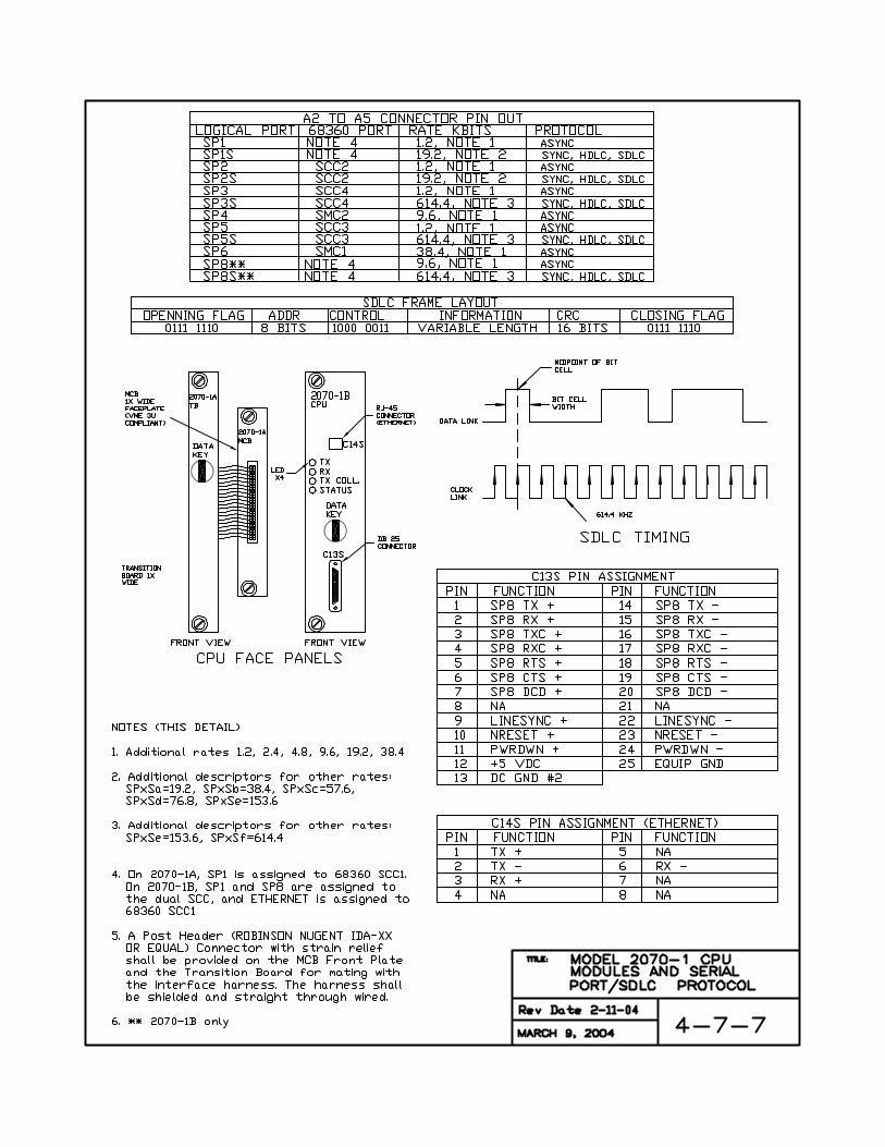


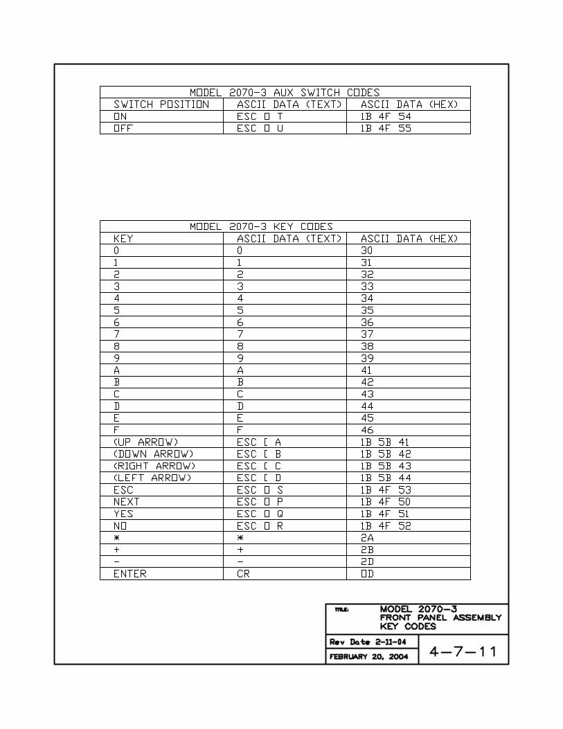


Standard for the ATC – Type 2070 March 12, 2004 99
5 TYPE 2070 PERIPHERAL EQUIPMENT GENERAL NOTES: 1. The 2070-6x and 2070-7x modules shall provide circuitry to disable its Channel 2 and
EIA-232 control lines (TX, RX, RTS, CTS, and DCD) when a ground true state is present at Connector A1, Pin B21 (C50 Enable). The disable lines shall be pulled up on this module
2. Line drivers/receivers shall be socket mounted or surface mounted. 3. Isolation circuitry shall be opto- or capacitive-coupled isolation technologies. Each
modules’s circuit shall be capable of reliably passing a minimum of 1.0 megabits per second.
4. The Comm modules shall be “Hot” swappable without damage to circuitry or
operations. 5.1 Type 2070-6 A & B Async/Modem Serial Comm Modules 5.1.1 Power Requirements A fused isolated +5 VDC with a minimum of 100 milliamperes power supply shall be provided for external use.
Option – Bourns MF – MSMD020 PTC (Positive Temperature Coefficient) Resettable Fuse, or approved equal, allowed.
5.1.2 Logic Switches Two LOGIC switches per circuit shall be provided (faceplate mounted). 5.1.2.1 One logic switch shall be used to vertically switch between Half-Duplex (Down) and Full-Duplex (Up). In Half-Duplex mode, the Transmit connections shall be used for both Receive and Transmit. 5.1.2.2 A MODEM Enable switch shall be provided such that when in the UP Position shall enable MODEM and disable MODEM in the DOWN Position.

Standard for the ATC – Type 2070 March 12, 2004 100
5.1.3 Circuitry Two circuits, designated CIRCUIT #1 and CIRCUIT #2, shall be provided. Both circuit functions shall be identical, except for their Serial Communications Port and external connector (CIRCUIT #1 to SP1 [or SP3] and C2S Connector and CIRCUIT #2 to SP2 [or SP4] and C20S Connector). The Circuits shall convert the 2070 UNIT Motherboard SP EIA-485 signals to/from board TTL level signals, isolate and drive the converted EIA-232 Signals interfacing with their associated MODEM and external connector. 5.1.3.1 Modem Requirements Each CIRCUIT shall have a MODEM with the following requirements:
1. Data Rate: Baud modulation of 300 to 1200 for Module 2070-6A and 0 to 9600 for Module 2070-6B.
2. Modulation: Phase coherent frequency shift keying (FSK). 3. Data Format: Asynchronous, serial by bit. 4. Line & Signal Requirements: Type 3002 voice-grade, unconditioned Tone
Carrier Frequencies (Transmit and Receive):2070-6A - 1.2 KHz MARK and 2.2 KHz SPACE, +/-1% tolerance. 2070-6B - 11.2 KHz MARK and 17.6 KHz SPACE, +/-1% tolerance. The operating band shall be (half power, -3 dB) between 1.0 KHz & 2.4 KHz for 2070-6A and 9.9 KHz & 18.9 KHz for 2070-6B.
5. Transmitting Output Signal Level: 0, -2, -4, -6, and -8 dB (at 1.7 KHz for 2070-6A & 14.7 KHz for 2070-6B) continuous or switch selectable.
6. Receiver Input Sensitivity: 0 to -40 dB. 7. Receiver Bandpass Filter: Shall meet the error rate requirement specified
below and shall provide 20 dB/octave, minimum active attenuation for all frequencies outside the operating band.
8. Clear-to-Send (CTS) Delay: 11 +/-3 milliseconds. 9. Receive Line Signal Detect Time: 8 +/-2 milliseconds mark frequency. 10. Receive Line Squelch: 6.5 (+/-1) milliseconds, 0 milliseconds (OUT). 11. Soft Carrier Turn Off Time: 10 +/-2 milliseconds (0.9 kilohertz for 2070-
6A and 7.8 kilohertz for 2070-6B). When the RTS is unasserted, the carrier shall turn off or go to soft carrier frequency.
12. Modem Recovery Time: Capable of receiving data within 22 milliseconds after completion of transmission.
13. Error Rate: Shall not exceed 1 bit in 100 kilobits, with a signal-to-noise ratio of 16 dB measured with flat-weight over a 300 to 3,000 Hertz band.
14. Transmit Noise: Less than -50 dB across 600-ohms resistive load within the frequency spectrum of 300 to 3,000 Hertz at maximum output.
15. Modem interface: EIA-232 Standards.

Standard for the ATC – Type 2070 March 12, 2004 101
5.1.4 Control Switch A CONTROL switch shall be provided on the module front panel to turn ON (Up) / OFF (Down) all module power. 5.2 Type 2070-7A & 7B Async Serial Comm Module
5.2.1 Circuitry Two circuits, designated CIRCUIT #1 and CIRCUIT #2, shall be provided. Their functions are identical, except for the CPU Serial Communications Port and external connector (CIRCUIT #1 to SP1 [or SP3] and Connector C21S and CIRCUIT #2 to SP2 [or SP4] and Connector C22S). 5.2.2 2070 -7A Each circuit shall convert its EIA-485 signal lines (RX, TX, RTS, CTS and DCD) to / from board TTL Level Signals; isolate both signal and ground; and drive / receive external EIA-232 devices via C21 / C22 Connectors. Connectors shall be DB-9S type. 5.2.3 2070 - 7B Each circuit EIA -485 signal lines, (RX, TX, TXC (I), TXC (O) and RXC) and associated signal ground shall be board terminated to matching drivers/receivers; isolated both signal and ground, and drive/receiver external EIA-485 devices via C21/C22 Connectors. Connectors shall be DB-15S type. 5.2.4 Indicators Each circuit signal TX and RX line shall have an LED Indicator mounted on the front plate and labeled to function. 5.3 Reserved for Future 2070-6D Fiber Optic Module This section is reserved for future fiber optic communication module requirements. 5.4 Reserved for Future 2070-6E Ethernet Module This section is reserved for future Ethernet communication module requirements.
Standard for the ATC – Type 2070 March 12, 2004 102
5.5 Chapter Details
TABLE OF CONTENTS
Type 2070-6 - Async/Modem Serial Comm Module 5-5-1 Type 2070-7 - Serial Comm Module 5-5-2 Type 2070-6D - Fiber Optic Comm Module (Future) 5-5-3 Type 2070-6E - Ethernet Comm Module (Future) 5-5-4 Section Notes: All dimensions are in millimeters. Module sheet metal tolerance shall be 0.38 mm or less.


Standard for the ATC – Type 2070 March 12, 2004 103
6 NEMA MODULE 6.1 Type 2070N Controller Unit 6.1.1 General This specification covers two versions of Type 2070 / NEMA Standard Controller Units. The versions associate with NEMA TS1 and NEMA TS2 Type 1 Standards. They are as follows: Type 2070 (V or L) N1 Controller Unit (TS1) Type 2070 (V or L) N2 Controller Unit (TS2-1) 6.1.2 Type 2070 (V or L) N1 Controller Unit The Type 2070 (V or L) N1 CONTROLLER UNIT consists of:
Unit CHASSIS Type 2070-1A or 1B - CPU Module Type 2070-2B - Field I/O Module Type 2070-3B - Front Panel Module Type 2070-4N (A or B) - Power Supply Module Type 2070-5 - VME Cage Assembly, if required Type 2070-8 - Field I/O Module
6.1.3 Type 2070 (V or L) N2 Controller Unit The Type 2070 (V or L) N2 CONTROLLER UNIT consists of:
Unit CHASSIS Type 2070-1A or 1B - CPU Module Type 2070-2N - Field I/O Module Type 2070-3B - Front Panel Module Type 2070-4N (A or B) - Power Supply Module Type 2070-5 - VME Cage Assembly, if required
6.1.4 Serial Port 5 Frame Address The Serial Port 5 Frame Address for 2070-2N and 2070-8 shall be “20”. 6.2 2070-2N FIELD I/O MODULE 6.2.1 Interfaces The 2070-2N Field I/O Module provides a TS2-1 compatible SDLC interface via 2070 Serial Port 3, AC Power to the 2070 Unit and Fault Monitor Logic Output via 2070 Serial Port 5 and Output Frame Byte 9 Bit 6 to the NEMA TS2 Cabinet Monitor Unit (CMU).

Standard for the ATC – Type 2070 March 12, 2004 104
6.2.2 Type 2070-2N Module Requirements The Module shall meet the 2070–2A Module Requirements with the following exceptions: No C1, C11 and C12 Connectors on the front panel of the module No 64 inputs / 64 outputs requirements Serial Port 5 routed to the FCU MPU Device only Serial Port 3 shall not have a disabling switch 6.2.3 Physical The module shall be a 4X type board / front panel with three connectors. The connectors are 10 Pin Connector A, a NEMA 5-15 Receptacle and a 15 Pin DB 15S C14 Connector. 6.2.4 Power Incoming 2070 AC Power is derived from Connector A Pin C (AC+), Pin A (AC-), and Pin H (Equipment Ground). The power is directly routed to the NEMA 5-15 Receptacle. Connector A shall intermate with a NEMA TS2 Type 1 (MS3106O-18-1S) cable. 6.2.5 Serial Port 3 Isolation The module shall isolate 2070 Serial Port 3 from the A3 Connector and reconvert the lines to external EIA 485 drivers/receivers which shall be terminated at C14 Connector. The Port shall be clocked at 153.6 kilobits per second. 6.2.6 FCU Output An FCU output shall drive a open collector transistor whose output shall be routed to Connector A Pin F for use as a FAULT MONITOR Output. The transistor shall be capable of sinking 200 milliamperes at 30 VDC. 6.2.7 Connector Pin Assignments Connectors A and C14 pin out and functions are as follows: Connector A
Pin Function Pin Function Pin Function
A AC Neutral E NA I NA B NA F Fault Monitor J NA C AC Line G DC#2 Ground D NA H Equip Ground

Standard for the ATC – Type 2070 March 12, 2004 105
Connector C14S
Pin Function Pin Finction Pin Function
1 TX Data+ 6 DC Ground 11 TX Clock - 2 DC Ground 7 RX Clock + 12 Equip Ground 3 TX Clock+ 8 DC Ground 13 RX Data - 4 DC Ground 9 TX Data - 14 NA 5 RX Data+ 10 NA 15 RX Clock –
6.2.8 TS2 BIU Control Serial Port 3 shall control the TS2 BIU Units using SDLC Protocol that meets the NEMA TS2 Type 1 Frame Command / Response Standards. 6.3 2070-4N (A or B) POWER SUPPLY MODULE 6.3.1 Requirements The 2070-4N Power Supply Module supports the NEMA TS1 and TS2 Standards. The module is identical to the 2070-4N (A and B) Power Supply Requirements except for the following:
1) The power cord shall have a 15 inch +/- 1 inch length as measured from the panel to the plug tips.
2) The AC Power Fail voltage shall be 85VAC +/-2VAC. 3) The AC Power Restore voltage shall be 90VAC +/-2VAC. 4) The 2070-4N (A or B) power supply shall have proper marking Example
“2070 4N (A or B)”. A permanent sticker shall be an acceptable marking method.
6.4 Type 2070- 8 Field I/O Module 6.4.1 Type 2070-8 Field I/O Module The Module shall consist of the Module Chassis, Module Power Supply, FCU Controller, Parallel Input/Output Ports, Serial Communications Circuits and Module Connectors. The Module CHASSIS shall be made of 0.06-inch minimum aluminum sheet and treated with clear chromate. All external screws, except where called out, shall be countersunk and shall be Phillips flat head stainless steel. The matching nuts shall be permanently captive on the mating surfaces.

Standard for the ATC – Type 2070 March 12, 2004 106
6.4.2 Module Front Panel The MODULE FRONT PANEL shall be furnished with the following:
1. ON/OFF POWER Switch mounted vertically with ON in the UP position. 2. LED DC Power Indicator. The indicator shall indicate that the required
+ 5 VDC is within 5% and the +24 VDC is within 8%. 3. Incoming VAC fuse protection. 4. Two DB-25S COMM connectors labeled "EX1" & "EX2." 5. Four NEMA Connectors A, B, C, & D.
6.4.3 Label A permanent LABEL shall be affixed to the Front Panel. The label shall display the unit's serial number. The number shall be permanent and easy to read. 6.4.4 Module Power Supply A MODULE POWER SUPPLY shall be provided and located on the right side of the module as viewed from the front. The supply shall provide the necessary module internal circuitry DC power plus 2.0 Amperes minimum of +24 VDC for external logic, detector inputs, and output load control. The supply shall meet the following requirements: 6.4.4.1 Input Protection Specification 4.5.3 INPUT PROTECTION 6.4.4.2 Power Supply Requirements Specification 4.5.6 POWER SUPPLY REQUIREMENTS except Specification 4.5.3. 6.4.4.3 DC Voltage Tolerances DC Voltage tolerances shall be +/-3%. 6.4.5 Incoming AC Power The supplied INCOMING AC POWER shall be derived from Connector A Pins "p" (AC+) and "U" (AC Neutral). External +24 VDC shall be at Connector A, Pin "B" and Connector D Pin "NN." AC Power for the 2070 receptacle shall be tapped off from the secondary side of the ON Switch / Fuse configuration. 6.4.6 Module PC Boards A MODULE PC Boards shall be mounted vertically.

Standard for the ATC – Type 2070 March 12, 2004 107
6.4.7 Power Down, NRESET, and LINESYNC Power Down, NRESET, and LINESYNC shall be routed to the module via C12 Connector. The state of the module output ports at the time of Power Down transition to LOW State and until NRESET goes HIGH shall be an open circuit. 6.4.8 Compliance with Type 2070-2 Field I/O Requirements The Module shall meet all requirements under 4.3 with the following exceptions: 6.4.8.1 Parallel Ports Parallel Ports, consisting of 118 Bits of Input and 102 bits of Output, shall be provided. Specification for inputs applies except the voltage is +24 in lieu of +12 and Ground False, "0," exceeds 16.0 VDC. LINESYNC signal is incoming in differential logic. 6.4.8.2 Serial Communication Circuitry The module shall interface with the 2070-2B Field I/O module via HAR 1 Harness meeting EIA-485 Requirements. All signal lines shall be isolated. HAR 1 Harness shall be 17 lines minimum with a C12P Connector on one end and soldered with strain relief on the other. In addition to the Controller interface, the EIA-485 Signal lines shall be routed to EX1 Connector. All necessary driver/receiver and isolation circuitry shall be provided. 6.4.9 EIA-232 Serial Port An EIA-232 Serial Port shall be provided with rate selection by jumper of 0.3, 1.2, 2.4, 4.8, 9.6, 19.2, & 38.4 kilobits per second asynchronous and shall be connected at EX1 Connector. 6.4.10 HAR 2 Harness A 22-line minimum HAR 2 Harness shall be provided between EX2 Connector and Model 2070-6 Serial COMM Module in the Type 2070 UNIT. This provides two Modems or EIA-232 Interfaces with the 2070 UNIT and the outside world. 6.4.11 Fault and Voltage Monitor FAULT and VOLTAGE MONITOR circuitry – NEMA TS1 Controller FAULT and VOLTAGE MONITOR functions (outputs to cabinet monitor) shall be provided. 6.4.11.1 Two 3-input OR gates shall be provided. The gate 1 output shall be connected to Connector A, Pin A (FAULT MONITOR) and gate 2 output shall be connected to

Standard for the ATC – Type 2070 March 12, 2004 108
Connector A, Pin C. Any FALSE state input shall cause a gate output FALSE (+24VDC) state. 6.4.11.2 The FCU Port 10, Bit 7 output shall normally change its state every 100 milliseconds. A MODULE Watchdog (WDT) circuit shall monitor the output. No state change for 2 +/-0.1 seconds shall cause the circuit output to generate a FALSE (+24 VDC) output (input to gates 1 and 2). Should the FCU begin changing state, the WDT output shall return to TRUE (0 VDC) state. 6.4.11.3 The module shall have a +5 VDC monitoring circuit which monitors the module’s +5 VDC (+/-0.25). If the voltage exceeds the limits, the circuit output shall generate a FALSE output (input to gates 1 and 2). Normal operation shall return the output state to TRUE state. 6.4.11.4 The FCU microprocessor output shall be assigned to FAULT Monitor (input to gate 1) and another output shall be assigned to VOLTAGE Monitor (input to gate 2). 6.4.11.5 CPU Port 5 SET OUTPUT COMMAND Message OUTPUTs O78 and O79 shall be assigned to FAULT (O78) and VOLTAGE (O79). The bit logic state “1” shall be FCU output FALSE. 6.4.11.6 CPU / FCU operation at POWER UP shall be as follows:
1. FCU Comm Loss Flag set. FAULT and VOLTAGE MONITOR outputs set to FALSE state.
2. CPU REQUEST MODULE STATUS COMMAND Message with “E” bit set is sent to FCU to clear Comm Loss Flag and responds to CPU with “E” bit reset.
3. Before the Comm Loss timer expires, the SET OUTPUT COMMAND data must be sent. In that data, the 078 and 079 logically set to “0” will cause the FCU microprocessor port pins assigned for FM and VM outputs to go to their TRUE state. At this point, the signal outputs defined in the message will be permitted at the output connectors. Any number of other messages may be sent between the MODULE STATUS COMMAND and SET OUTPUTS COMMAND.

Standard for the ATC – Type 2070 March 12, 2004 109
4. If the above message sequence is not followed, Comm Loss Flag shall be set (or remain) and VM & FM shall retain the FALSE output state.
5. Performs items 2 & 3 above User Software.
6.4.11.7 A CPU / FCU Communications Loss during normal operation shall cause all outputs to go blank (FALSE state) and shall set the Comm Loss Flag. FM and VM outputs shall be in FALSE state. 6.5 Chapter Details
TABLE OF CONTENTS
MODEL 2070N1 - Front View 11-5-1 MODEL 2070N1 - Side View 11-5-2 MODEL 2070N1 - Isometric View 11-5-3 MODEL 2070N1 - 2070-8 Field I/O Module, Connectors A & B 11-5-4 MODEL 2070N1 - 2070-8 Field I/O Module, Connectors C & D 11-5-5 MODEL 2070N1 - 2070-8 Field I/O Module, EX1 & EX2 Connectors 11-5-6 Section Notes: All dimensions are in millimeters. Module sheet metal tolerance shall be 0.38 mm or less.


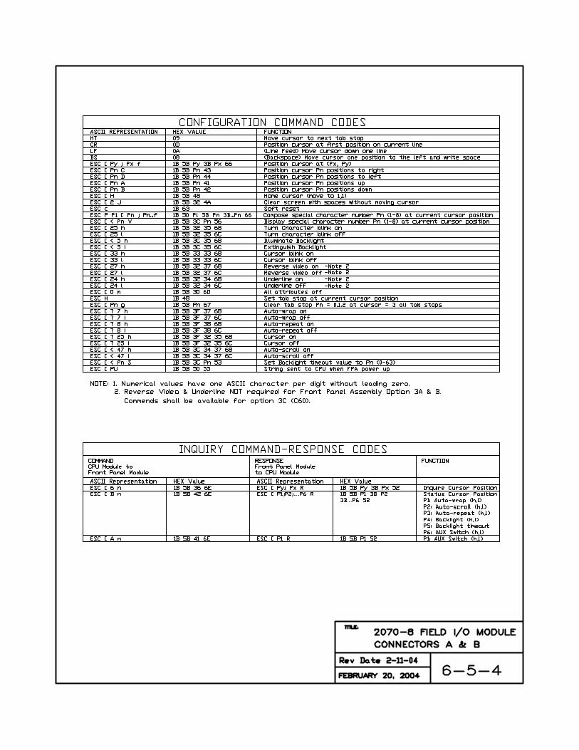


Standard for the ATC – Type 2070 March 12, 2004 110
7 GLOSSARY 7.1.1 Terms and Abbreviations Wherever the following terms or abbreviations are used, the intent and meaning shall be interpreted as follows: A - Ampere AC - Alternating Current AC+ - 120 Volts AC, 60 hertz ungrounded power source AC- - 120 Volts AC, 60 hertz grounded return to the power
source AGENCY - The AGENCY director, acting either directly or through
properly authorized agents, such agents acting within the scope of the particular duties delegated to them.
ANSI - American National Standard Institute ASCII - American Standard Code for Information Interchange Assembly - A complete machine, structure or unit of a machine that
was manufactured by fitting together parts and/or modules ASTM - American Society for Testing and Materials AWG - American Wire Gage C - Celsius C Language - The ANSI C Programming Language Cabinet - An outdoor enclosure generally housing the controller unit
and associated equipment Certificate of - A certificate signed by the manufacturer of the material or
the Compliance manufacturer of assembled materials stating that the
materials involved comply in all respects with the requirements of the specifications
Channel - An information path from a discrete input to a discrete
output.

Standard for the ATC – Type 2070 March 12, 2004 111
Component - Any electrical or electronic device Contractor - The person or persons, Manufacturer, firm, partnership,
corporation, vendor or combination thereof, who have entered into a contract with the AGENCY, as party (s) of the second part or legal representative
Controller Unit - That portion of the controller assembly devoted to the
operational control of the logic decisions programmed into the assembly
CPU - Central Processing Unit CTS - Clear To Send DAT Program - The AGENCY’s Diagnostic and Acceptance Test Program dB - Decibel dBa - Decibels above reference noise, adjusted DC - Direct Current DCD - Data Carrier Detect (Receive Line Signal Detector) DIN - Deutsche Industrie Norm DRAM - Dynamic random access memory. Random access means
that the processor can access any part of the memory or data storage space directly rather than having to proceed sequentially from some starting place. DRAM is dynamic in that it needs to have its storage cells refreshed or given a new electronic charge every few milliseconds.
EG - Equipment Ground EIA - Electronic Industries Association EMI - Electro Magnetic Interference EPROM - Ultraviolet Erasable, Programmable, Read Only Memory
Device

Standard for the ATC – Type 2070 March 12, 2004 112
EEPROM - Electrically Erasable, Programmable, Read Only Memory Device
Equal - Connectors: comply to physical dimensions, contact
material, plating and method of connection. Devices: comply to function, pin out, electrical and operating parameter requirements, access times and interface parameters of the specified device
ETL - Electrical Testing Laboratories, Inc. Firmware - A computer program or software stored permanently in
PROM, EPROM, ROM or semi-permanently in EEPROM FLASH - A +5 VDC powered IC Memory Device with nonvolatile,
electrically erasable, programmable, 100K read/write minimum cycles and fast access time features
FPA - Front Panel Assembly HEX - Hexadecimal Hz - Hertz IC - Integrated Circuit I.D. - Identification IEEE - Institute of Electrical and Electronics Engineers ISO - Isolated Jumper - A means of connecting/disconnecting two or more
conductive by soldering/desoldering a conductive wire or by PCB post jumper
KB - Kilobytes Keyed - Means by which like connectors can be physically altered
to prevent improper insertion. Laboratory - The established laboratory of the AGENCY or other
laboratories authorized by the AGENCY to test materials involved in the contract
LCD - Liquid Crystal Display

Standard for the ATC – Type 2070 March 12, 2004 113
LED - Light Emitting Diode LOGIC - Negative Logic Convention (Ground True) State LSB - Least Significant Byte lsb - Least Significant Bit MB - megabyte MSB - Most Significant Byte msb - Most Significant Bit m - Milli MCU/MPU/ - Micro Controller Unit, Microprocessor Unit, or Integrated IMP Multiprotocol Processor MIL - Military Specifications MODEM - Modulation/Demodulation Unit Module - A functional unit that plugs into an assembly Motherboard - A printed circuit connector interface board with no active
or passive components MOS - Metal-Oxide Semiconductor MOV - Metal-Oxide Varistor MS - Military Standards N - Newton: SI unit of force N.C. - Normally closed contact N.O. - Normally open contact NA - Presently Not Assigned. Cannot be used by the
Manufacturer for other purposes NEMA - National Electrical Manufacturer's Association

Standard for the ATC – Type 2070 March 12, 2004 114
NETA - National Electrical Testing Association, Inc. n - nano NLSB - Next Least Significant Byte nlsb - Next Least Significant Bit NMSB - Next Most Significant Byte nmsb - Next Most Significant Bit PCB - Printed Circuit Board PDA - Power Distribution Assembly PLA/PAL - Programmable Array Logic Device Power Failure - A Power Failure is said to have occurred when the
incoming line voltage falls below 92 +/- 2 VAC for 50 milliseconds. See Power Conditions.
Power - Power is said to be restored when the incoming line voltage
equals Restoration or exceeds 97 +/- 2 VAC for 50 milliseconds. See Power
Conditions. Power - 16.7 ms (one 60 Hertz cycle) reaction period is allowed to
be Conditions included in the 50 milliseconds timing or added to (67
milliseconds duration). The hysteresis between power failure and power restoration voltage settings shall be a min. of 5 VAC with a threshold drift of no more than 0.2 VAC.
ppm - Parts per million PWM - Pulse Width Modulation RAM - Random Access Memory RF - Radio Frequency RMS - Root-Mean-Square

Standard for the ATC – Type 2070 March 12, 2004 115
ROM - Read Only Memory Device RTS - Request to Send R/W - Controller Unit Read/Write Control Line RxD - Received Data SCI - Serial Communications Interface SDLC - Synchronous Data Link Control S - Logic State s - second Second Sourced - Produced by more than one Manufacturer SRAM - Static Random Access Memory Device SW - Switch TB - Terminal Block TOD - Time Of Day Clock Triac - Silicon-Controlled Rectifier which controls power
bilaterally in an AC switching circuit TTL - Transistor-Transistor Logic Thumb Screw - (TSD ) A retractable screw fastener with projecting Device stainless steel screw, spring and natural aluminum knob
finish. (TSD No.2 shall be flat black.) TSD No.1 - 8-32 SOUTHCO #47-62-301-20 or equal. TSD No.2 - 8-32 SOUTHCO #47-62-301-60 or equal. TSD No.3 - M3 SOUTHCO #47-82-101-10 or equal. TxD - Transmitted Data u - Micro UL - Underwriter's Laboratories, Inc. VAC - Voltage Alternating Current (root mean square)
Standard for the ATC – Type 2070 March 12, 2004 116
VDC - Voltage Direct Current VME - Versa Module Eurocard, VMEbus Standard IEEE
P1014/D1.2 x - Number Value XX - Manufacturer's Option WDT - Watchdog Timer: A monitoring circuit, external to the
device watched, which senses an Output Line from the device and reacts