a viable realization of vedic multipliers using reversible … · · 2015-11-24a viable...
TRANSCRIPT

IJCSIET-- International Journal of Computer Science information and Engg., Technologies ISSN 2277-4408 || 01092015-058
IJCSIET-ISSUE5-VOLUME3-SERIES1 Page 1
A Viable Realization of Vedic Multipliers Using Reversible Gate Approach 1Singuru roja, 2Darsi syambabu 1Student, 2Assistant Professor
1,2Sri Venkateswara College Of Engineering & Technology, Srikakulam, Andhra Pradesh, INDIA [email protected],
ABSTRACT
Multiplier design is always a challenging task; however many designs are proposed,
the user needs demands much more optimized ones. Vedic mathematics provides some
algorithms that evaluate fast results, both in mental calculations or hardware design. Power
dissipation is continuously reduced by the use of Reversible logic. The reversible Urdhva
Tiryakbhayam Vedic multiplier is one such multiplier which is effective both in terms of speed
and power. In this paper the modified design increase the performance by maintain the design
functionality without any degradation. The Total Reversible Logic Implementation Cost
(TRLIC) evaluates the proposed design. This multiplier has application over designing Fast
Fourier Transforms (FFTs) Filters and other applications of DSP like imaging, software defined
radios, wireless communications.
KEYWORDS: REVESIBLE GATES, Urdhva Tiryakbhayam , Vedic mathematics.
1. INTRODUCTION
High speed arithmetic operations are
very important in many signal processing
applications. Speed of the digital signal
processor (DSP) is largely determined by
the speed of its multipliers. In fact the
multipliers are the most important part of
all digital signal processors; they are very
important in realizing many important
functions such as fast Fourier transforms
and convolutions. Since a processor
spends considerable amount of time in
performing multiplication, an
improvement in multiplication speed can
greatly improve system performance.
Multiplication can be implemented using
many algorithms such as array, booth,
carry save, and Wallace tree algorithm.
The computational time required by the
array multiplier is less because the partial
products are computed independently in
parallel. The delay associated with the
array multiplier is the time taken by the
signals to propagate through the gates that
form the multiplication array.
Arrangement of adders is another way
of improving multiplication speed. There
are two methods for this: Carry save array
(CSA) method and Wallace tree method.
In the CSA method, bits are processed one
by one to supply a carry signal to an adder
located at a one bit higher position. The
CSA method has got its own limitations
since the execution time depends on the
number of bits of the multiplier. In the
Wallace tree method, three bit signals are
passed to a one bit full adder and the sum
is supplied to the next stage full adder of
the same bit and the carry output signal is
passed to the next stage full adder of same
number of bit and the then formed carry is
supplied to the next stage of the full adder
located at a one bit higher position. In this
method, the circuit lay out is not easy.
IJCSIET-- International Journal of Computer Science information and Engg., Technologies ISSN 2277-4408 || 01092015-058
IJCSIET-ISSUE5-VOLUME3-SERIES1 Page 2
Booth algorithm reduces the number
of partial products. However, large booth
arrays are required for high speed
multiplication and exponential operations
which in turn require large partial sum and
partial carry registers. Multiplication of
two n-bit operands using a radix-4 booth
recording multiplier requires
approximately n/ (2m) clock cycles to
generate the least significant half of the
final product, where m is the number of
booth recoded adder stages. Thus, a large
propagation delay is associated with this
case. The modified booth encoded Wallace
tree multiplier uses modified booth
algorithm to reduce the partial products
and also faster additions are performed
using the Wallace tree
A binary multiplier is an electronic
circuit used in digital electronics, such as a
computer, to multiply two binary numbers.
It is built using binary adders. A variety of
computer arithmetic techniques can be
used to implement a digital multiplier.
Most techniques involve computing a set
of partial products, and then summing the
partial products together. This process is
similar to the method taught to primary
schoolchildren for conducting long
multiplication on base-10 integers, but has
been modified here for application to a
base-2 (binary) numeral system. Until the
late 1970s, most minicomputers did not
have a multiply instruction, and so
programmers used a "multiply routine"
which repeatedly shifts and accumulates
partial results, often written using loop
unwinding. Mainframe computers had
multiply instructions, but they did the
same sorts of shifts and adds as a
"multiply routine". Early microprocessors
also had no multiply instruction. The
Motorola 6809, introduced in 1978, was
one of the earliest microprocessors with a
dedicated hardware multiply instruction. It
did the same sorts of shifts and adds as a
"multiply routine", but implemented in the
microcode of the MUL instruction.
As more transistors per chip
became available due to larger-scale
integration, it became possible to put
enough adders on a single chip to sum all
the partial products at once, rather than
reuse a single adder to handle each partial
product one at a time. Because some
common digital signal processing
algorithms spend most of their time
multiplying, digital signal processor
designers sacrifice a lot of chip area in
order to make the multiply as fast as
possible; a single-cycle multiply–
accumulate unit often used up most of the
chip area of early DSPs.
2. Vedic mathematics:
Vedic Mathematics is one of the most
ancient methodologies used by the Aryans
in order to perform mathematical
calculations. This consists of algorithms
that can boil down large arithmetic
operations to simple mind calculations.
The above said advantage stems from the
fact that Vedic mathematics approach is
totally different and considered very close
to the way a human mind works. The
efforts put by Jagadguru Swami Sri
Bharati Krishna Tirtha Maharaja to
introduce Vedic Mathematics to the
commoners as well as streamline Vedic
Algorithms into 16 categories or Sutras
needs to be acknowledged and
appreciated. The Urdhva Tiryakbhayam is
IJCSIET-- International Journal of Computer Science information and Engg., Technologies ISSN 2277-4408 || 01092015-058
IJCSIET-ISSUE5-VOLUME3-SERIES1 Page 3
one such multiplication algorithm which is
well known for its efficiency in reducing
the calculations involved.
With the advancement in the VLSI
technology, there is an ever increasing
quench for portable and embedded Digital
Signal Processing (DSP) systems. DSP is
omnipresent in almost every engineering
discipline. Faster additions and
multiplications are the order of the day.
Multiplication is the most basic and
frequently used operations in a CPU.
Multiplication is an operation of scaling
one number by another. Multiplication
operations also form the basis for other
complex operations such as convolution,
Discrete Fourier Transform, Fast Fourier
Transforms, etc. With ever increasing need
for faster clock frequency it becomes
imperative to have faster arithmetic unit.
Therefore, DSP engineers are constantly
looking for new algorithms and hardware
to implement them.
Vedic mathematics can be aptly employed
here to perform multiplication. Another
important area which any DSP engineer
has to concentrate is the power dissipation,
the first one being speed. There is always a
trade off between the power dissipated and
speed of operation. The reversible
computation is one such field that assures
zero power dissipation. Thus during the
design of any reversible circuit the delay is
the only criteria that has to be taken care
of. In a reversible Urdhva Tiryakbhayam
Multiplier had been proposed.
2.1. Reversible Logic Gates: A reversible logic gate is an n-input n-
output logic device with one-to-one
mapping. This helps to Determine the
outputs from the inputs and also the inputs
can be uniquely recovered from the
outputs. Also in the synthesis of reversible
circuits direct fan-out is not allowed as
one–to-many concept is not reversible.
However fan out in reversible circuits is
achieved using additional gates. A
reversible circuit should be designed using
minimum number of reversible logic
gates. From the point of view of reversible
circuit design, there are many parameters
for determining the complexity and
performance of circuits.
The number of Reversible gates (N):
The number of reversible gates used in
circuit.
The number of constant inputs (CI):
This refers to the number of inputs that are
to be maintained constant at either 0 or 1
in order to synthesize the given logical
function.
The number of garbage outputs (GO):
This refers to the number of unused
outputs present in a reversible logic
circuit. One cannot avoid the garbage
outputs as these are very essential to
achieve reversibility.
Quantum cost (QC): This refers to the
cost of the circuit in terms of the cost of a
primitive gate. It is calculated knowing the
number of primitive reversible logic gates
(1*1 or 2*2) required to realize the circuit.
Gate levels (GL): This refers to the
number of levels in the circuit which are
required to realize the given logic
functions .
Total Reversible Logic Implementation
Cost (TRLIC) : Let, in a reversible logic
circuit there are NG reversible logic gates,
IJCSIET-- International Journal of Computer Science information and Engg., Technologies ISSN 2277-4408 || 01092015-058
IJCSIET-ISSUE5-VOLUME3-SERIES1 Page 4
CI constant inputs, GO number of garbage
outputs, and have a quantum cost QC.
In this, an improved design of
reversible multiplier with respect to its
previous counterparts is proposed.
Multiplier circuits play an important role
in computational operation using
computers. There are many arithmetic
operations which are performed, on a
computer ALU, through the use of
multipliers. Design and implementation of
digital circuits using reversible logic has
attracted popularity to gain entry into the
future computing technology.
2.2. Basic reversible logic gates::
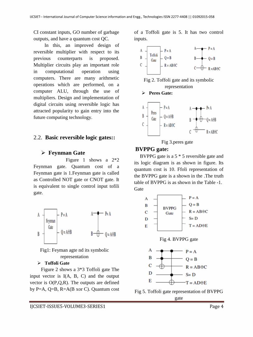
Feynman Gate
Figure 1 shows a 2*2
Feynman gate. Quantum cost of a
Feynman gate is 1.Feynman gate is called
as Controlled NOT gate or CNOT gate. It
is equivalent to single control input tofili
gate.
Fig1: Feyman agte nd its symbolic
representation
Toffoli Gate
Figure 2 shows a 3*3 Toffoli gate The
input vector is I(A, B, C) and the output
vector is O(P,Q,R). The outputs are defined
by P=A, Q=B, R=A(B xor C). Quantum cost
of a Toffoli gate is 5. It has two control
inputs.
Fig 2. Toffoli gate and its symbolic
representation
Peres Gate:
Fig 3.peres gate
BVPPG gate:
BVPPG gate is a 5 * 5 reversible gate and
its logic diagram is as shown in figure. Its
quantum cost is 10. Ffoli representation of
the BVPPG gate is a shown in the .The truth
table of BVPPG is as shown in the Table -1.
Gate
Fig 4. BVPPG gate
Fig 5. Toffoli gate representation of BVPPG
gate
IJCSIET-- International Journal of Computer Science information and Engg., Technologies ISSN 2277-4408 || 01092015-058
IJCSIET-ISSUE5-VOLUME3-SERIES1 Page 5
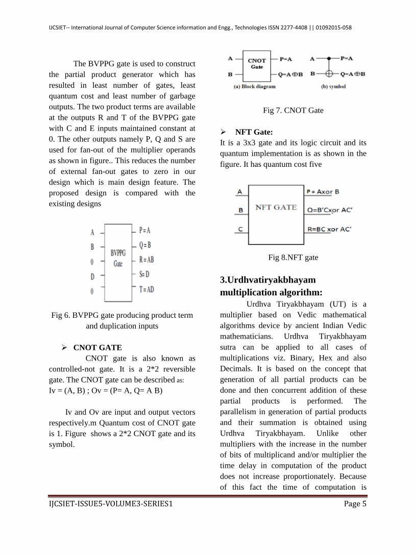
The BVPPG gate is used to construct
the partial product generator which has
resulted in least number of gates, least
quantum cost and least number of garbage
outputs. The two product terms are available
at the outputs R and T of the BVPPG gate
with C and E inputs maintained constant at
0. The other outputs namely P, Q and S are
used for fan-out of the multiplier operands
as shown in figure.. This reduces the number
of external fan-out gates to zero in our
design which is main design feature. The
proposed design is compared with the
existing designs
Fig 6. BVPPG gate producing product term
and duplication inputs
CNOT GATE
CNOT gate is also known as
controlled-not gate. It is a 2*2 reversible
gate. The CNOT gate can be described as:
Iv = (A, B) ; Ov = (P= A, Q= A B)
Iv and Ov are input and output vectors
respectively.m Quantum cost of CNOT gate
is 1. Figure shows a 2*2 CNOT gate and its
symbol.
Fig 7. CNOT Gate
NFT Gate:
It is a 3x3 gate and its logic circuit and its
quantum implementation is as shown in the
figure. It has quantum cost five
Fig 8.NFT gate
3.Urdhvatiryakbhayam
multiplication algorithm:
Urdhva Tiryakbhayam (UT) is a
multiplier based on Vedic mathematical
algorithms device by ancient Indian Vedic
mathematicians. Urdhva Tiryakbhayam
sutra can be applied to all cases of
multiplications viz. Binary, Hex and also
Decimals. It is based on the concept that
generation of all partial products can be
done and then concurrent addition of these
partial products is performed. The
parallelism in generation of partial products
and their summation is obtained using
Urdhva Tiryakbhayam. Unlike other
multipliers with the increase in the number
of bits of multiplicand and/or multiplier the
time delay in computation of the product
does not increase proportionately. Because
of this fact the time of computation is
IJCSIET-- International Journal of Computer Science information and Engg., Technologies ISSN 2277-4408 || 01092015-058
IJCSIET-ISSUE5-VOLUME3-SERIES1 Page 6
independent of clock frequency of the
processor. Hence one can limit the clock
frequency to a lower value. Also, since
processors using lower clock frequency
dissipate lower energy, it is economical in
terms of power factor to use low frequency
processors employing fast algorithms like
the above mentioned. The Multiplier based
on this sutra has the advantage that as the
number of bits increases, gate delay and area
increases at a slow pace as compared to
other conventional multipliers.
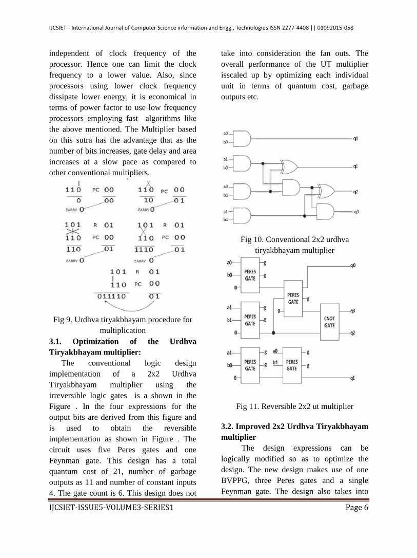
Fig 9. Urdhva tiryakbhayam procedure for
multiplication
3.1. Optimization of the Urdhva
Tiryakbhayam multiplier:
The conventional logic design
implementation of a 2x2 Urdhva
Tiryakbhayam multiplier using the
irreversible logic gates is a shown in the
Figure . In the four expressions for the
output bits are derived from this figure and
is used to obtain the reversible
implementation as shown in Figure . The
circuit uses five Peres gates and one
Feynman gate. This design has a total
quantum cost of 21, number of garbage
outputs as 11 and number of constant inputs
4. The gate count is 6. This design does not
take into consideration the fan outs. The
overall performance of the UT multiplier
isscaled up by optimizing each individual
unit in terms of quantum cost, garbage
outputs etc.
Fig 10. Conventional 2x2 urdhva
tiryakbhayam multiplier
Fig 11. Reversible 2x2 ut multiplier
3.2. Improved 2x2 Urdhva Tiryakbhayam
multiplier
The design expressions can be
logically modified so as to optimize the
design. The new design makes use of one
BVPPG, three Peres gates and a single
Feynman gate. The design also takes into
IJCSIET-- International Journal of Computer Science information and Engg., Technologies ISSN 2277-4408 || 01092015-058
IJCSIET-ISSUE5-VOLUME3-SERIES1 Page 7
account the fan outs. One of the major
design constraints of reversible logic is the
fan out, other being loops not permitted.
This means that the reversible logic circuit
with multiple numbers of same inputs is not
advisable. One way out is to use a separate
fan out generator or to build a circuit that
inherently takes care of fan outs using the
reversible logic gates used in the design.
This design has a quantum cost of 23,
number of garbage outputs as 5, number of
gates 5 and the number of constant inputs is.
The second design also considers the
fan out using BVPPG, three Peres gates and
one NFT gate as shown in the figure 5. The
quantum cost of the circuit is 24; number of
garbage outputs as 4, number of gates 5 and
the number of constant inputs is 5. I1, I2, I3
(Fig 5 and 6) and I4 (Fig 6) are the
intermediate outputs that are used for fan-
out purposes.
Fig 12. Proosed modified design 1
Fig 13. Proposed modified design 2
3.3.Design of 4x4 Urdhva Tiryakbhayam
multiplier
The Reversible 4X4 Urdhva
Tiryakbhayam Multiplier design emanates
from the 2X2 multiplier. The block diagram
of the 4X4 Vedic Multiplier is presented in
the figure 6. It consists of four 2X2
multipliers each of which procures four bits
as inputs; two bits from the multiplicand and
two bits from the multiplier. The lower two
bits of the output of the first 2X2 multiplier
are entrapped as the lowest two bits of the
final result of multiplication.
Two zeros are concatenated with the
upper two bits and given as input to the four
bit ripple carry adder. The other four input
bits for the ripple carry adder are obtained
from the second 2X2 multiplier. Likewise
the outputs of the third and the terminal 2X2
multipliers are given as inputs to the second
four bit ripple carry adder. The outputs of
these four bit ripple carry adders are in turn
5 bits each which need to be summed up.
This is done by a five bit ripple carry add
which generates a six bit output. These six
bits from the upper bits of the final result.

IJCSIET-- International Journal of Computer Science information and Engg., Technologies ISSN 2277-4408 || 01092015-058
IJCSIET-ISSUE5-VOLUME3-SERIES1 Page 8
The design shown in consists of only
HNG gates. The number of HNG gates is 4
if the ripple carry adder is used in the second
stage or five if the ripple carry adder is used
in the last stage of the 4X4 Urdhva
Tiryakbhayam Multiplier. The ripple carry
adder can be modified as under. Since for
any ripple carry adder the input carry for the
first full adder is zero, this implicitly means
the first adder is a half adder. Thus a Peres
gate can efficiently replace a HNG. This cut
down the quantum cost by two for any ripple
carry adder and the garbage output by one.
The Constant inputs and the gate count
remain unchanged.
Fig 14. Proposed modified 5 Brr Ripple
carry adder design
Fig 15. Proposed modified ripple carry
adder design
Since TRLIC is the sum of all these design
parameters, it is commendable of having a
least value of TRLIC The proposed design
of Reversible UT Multiplier is compared
with as many as 11 different prominent
multiplier designs in the literature in terms
of Quantum cost, garbage outputs, number
of gates, number of constant inputs and also
in terms of TRLIC values. This also includes
a comparison with our Own previous design
and the optimization is clearly evident from
the table of comparison.
4. RESULTS:
4.1. UT SCHEMATIC
4.2. UT RTL SCHEMATIC
IJCSIET-- International Journal of Computer Science information and Engg., Technologies ISSN 2277-4408 || 01092015-058
IJCSIET-ISSUE5-VOLUME3-SERIES1 Page 9
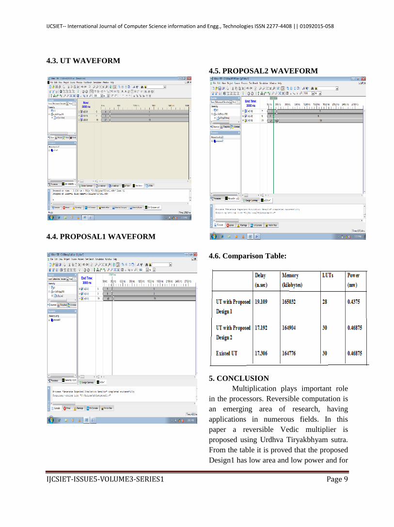
4.3. UT WAVEFORM
4.4. PROPOSAL1 WAVEFORM
4.5. PROPOSAL2 WAVEFORM
4.6. Comparison Table:
5. CONCLUSION
Multiplication plays important role
in the processors. Reversible computation is
an emerging area of research, having
applications in numerous fields. In this
paper a reversible Vedic multiplier is
proposed using Urdhva Tiryakbhyam sutra.
From the table it is proved that the proposed
Design1 has low area and low power and for
IJCSIET-- International Journal of Computer Science information and Engg., Technologies ISSN 2277-4408 || 01092015-058
IJCSIET-ISSUE5-VOLUME3-SERIES1 Page 10
the proposed Design2 has low delay. In this
project for simulation and for synthesis
Xilinx-ISE tool is used using target
technology and performing placing &
routing operation for system verification.
Proposal 1 power =0.4375mw
Proposal 2 power=0.46875mw
4*4 UT Multiplier=0.46875mw
6. REFERENCES
[1] Swami Bharati Krsna Tirtha, Vedic
Mathematics. Delhi: Motilal Banarsidass
publishers 1965
[2] Vedic Mathematics:
http://www.hinduism.co.za/vedic.html.
[3] R. Landauer,”Irreversibility and Heat
Generation in the Computational Process”,
IBM Journal of Research and Development,
5, pp.183-191, 1961.
[4] C.H. Bennett, “Logical reversibility of
Computation”, IBM J. Research and
Development, pp.525 532, November 1973.
[5] R. Feynman, “Quantum Mechanical
Computers,” Optics News, Vol.11, pp. 11–
20, 1985.
[6] A. Peres, Reversible logic and quantum
computers, Phys. Rev. A 32 (1985) 3266–
3276.
[7] E. Fredkin and T. Toffoli,”Conservative
Logic”, Int’l J. Theoretical Physics Vol 21,
pp.219-253, 1982.
[8] G Ganesh Kumarand V Charishma,
Design of high speed vedic multiplier using
vedic mathematics techniques, Itn’l J. of
Scientific and Research Publications, Vol. 2
Issue 3 March 2012
[9] Rakshith Saligram and Rakshith T.R.
“Design of Reversible Multipliers for linear
filtering Applications in DSP” VLSICS, Vol
3. No (6), Dec-12
[10] Rakshith Saligram and Rakshith T.R.
“Novel Code Converter Employing
Reversible Logic”, International Journal of
Computer Applications(IJCA),August 2012.
[11] H R Bhagyalakshmi and M K
Venkatesha,” Optimized multiplier using
Reversible Multi-Control Input Toffoli
Gates”, VLSICS, Vol 3. No (6), Dec.- 12
[12] Rakshith T R and Rakshith Saligram,
Design of High Speed Low Power
Multiplier using Reversible logic: a Vedic
Mathematical Approach, Intl. Conf. on
Circuit, Power and Computational
Technologies.
[13] H. R. Bhagyalakshmi, M. K.
Venkatesha, “An Improved Design of a
Multiplier using Reversible Logic Gates,”
IJEST, Vol. 2, No. 8, 2010.
[14] Fateme Naderpour, Abbas Vafaei
“Reversible Multipliers: Decreasing the
Depth of the Circuit” ICECE 2008, 20-22
December 2008.
Author’s Profile:
Mr.D.syam babu received the bachelor of
engineering degree in Electronics
Communication Engineering(ECE)
from JNTU hyderabad university in the
college Q.I.S.C.E.T,ongole and masters
degree (M.Tech) from JNTU kakinada
university in the college vignan's institute of
informationtechnology,visakhapatnam.
Currently he is working as assistant
professor in SVCET(SRI
VENKATESWARA COLLEGE OF
IJCSIET-- International Journal of Computer Science information and Engg., Technologies ISSN 2277-4408 || 01092015-058
IJCSIET-ISSUE5-VOLUME3-SERIES1 Page 11
ENGINEERING AND TECHNOLOGY)
Etcherla srikakulam A.P.His area of interests
are WIRELESS COMMUNICATIONS,
DIGITAL ELECTRONICS AND SIGNAL
PROCESSING.
Ms.S.roja received the bachelor of
engineering degree in Electronics
Communication Engineering (ECE)
from JNTU Kakinada university in the
college SSIT(sri sivani institute of
technology),srikakulam and masters degree
fromSVCET (SRI VENKATESWARA
COLLEGE OF ENGINEERING AND
TECHNOLOGY) Etcherla Srikakulam A.P.
Area of interest is VLSI designing.