a vlsi implementation of an adaptive-effort low-power viterbi decoder...
TRANSCRIPT

A VLSI IMPLEMENTATION OF AN ADAPTIVE-EFFORT LOW-POWER
VITERBI DECODER FOR WIRELESS COMMUNICATIONS
A thesis submitted to the Department of Electrical and Computer Engineering
in conformity with the requirements forthe degree of Master of Science
Queen's UniversityKingston, Ontario, Canada
copyright Gordon John Allan, 2001

Cellular Systems• Interference based• Increasing capacity• Push towards data-centric apps
f0 f1
f0 f1f0
f0
CDMA
FDM
• Inc. speed/function à higher MIPS• Higher MIPS à low battery life

Plethora of Standards
A non-exhaustive list of international mobile standards
Peer Bluetooth North A.+ to Tetra Europe The Terrestrial Trunked Radio Peer PHS Japan Personal Handy System
AMPS North A. Advanced Mobile Phone System 1G TACS Europe Total Access Communications System
J-TACS Japan Japanese Total Access Communications System NMT Nordic Nordic Mobile Telephone CDMA North A. Code Division Multiple Access (IS-95 Standard)
2G GSM Europe Global System for Mobile communications PDC/JDC Japan Personal Digital Cellular/Japan Digital Cellular CDMAone North A. IS-95 B Standard
2.5G GPRS Europe General Packet Radio Service - GSM w/ packets Edge Europe Enhanced Data rates for Global Evolution (384 kbps) cdma2000 North A. also known as Wideband CDMA
3G UMTS Europe Universal Mobile Telecommunications System NTT DoCoMo Japan
• Many different Wireless standards• Currently have 2.5G[eneration] networks available

Error Correcting Codes (ECC)•Wireless channel is quite harsh
•Use convolutional codes to protect ‘important’ data
•Strength of the code is mainly determined by its constraint length (K=9 in 3G below)
•Power hungry to decode – especially at high data rates

Effect of Constraint Length on Error Rate

Current Solutions• Current solutions implement the Viterbi algorithm on a DSP for the
channel decoder• K=9, 1 Mbps requires
625 MIPS - 235 mA – 117% capacity - TMS320VC5441154 Mhz - 81mA – 51% capacity – SC140
• Too power hungry as rates increase to 3G• Too MIPS intensive – can’t share DSP with other operations

Convolutional Coding/Decoding
1001100 0 0
X0
X1
1
1
1+3+2+1- 1- 2- 3
t
Logic
1
0
Y0 Y1
+1 +2
Digitized Symbols
Y0 Y1

Quantized Input: +1,+2 +1, -3 +1,-2 +3,+1 +2,-0 ...
11
01
00
11
00
11
10
10
01
10
01
00
11
01
10
00
Expexted
Branch
Symbo l s
Channel Symbols: 1,1 1,0 1,0 1,0 1,1 ...Input Data: 1 0 1 1 0 ...
000
001
010
011
100
101
110
111
time(t): 0 1 2 3 4 ...
4
0
6
4
+4
+3
+1
+0 +0
+3
+0
0
3
6
+1
+2
0
+2
+1
5
3
6+0
+3
6
9
5
+3
13
5
9
1
7
9
5
7
9
9
7
3
9
7
9
3
3
5
7
7
7
11
3
9
1
9
5
9
5
9
5
7
+3
+1
+3+1
+0
+2
Expected Symbol 0,0
Expected Symbol 1,1

Reduced Complexity Decoding
• Depth First– Fano
• Metric First– Stack
• Breadth First– T-Algorithm– M-Algorithm– Reduced State Sequence Detection (RSSD)

Reduce State Sequence Detection
• Form super-states,each contain contain many sub-states
• Effectively ‘neglect’ the p-least significant bits of the Tx shift register, treating the code ‘as if’ it were of length K’ = K-p
• Cost is reduced error performance
• Complexity/Power is reduced by 2p

Further Reduction

Error Performance of RSSDFER vs SNR for RSSD in Fading Channel
1.E-05
1.E-04
1.E-03
1.E-02
1.E-01
1.E+002 4 6 8 10 12 14
SNR
FER
(102
4 bi
t fra
mes
) 481632641282565121024

Error Performance of RSSDFER vs SNR for the AWGN Channel
1.E-05
1.E-04
1.E-03
1.E-02
1.E-01
1.E+000 1 2 3 4 5
SNR
FER
481632641282565121024

Other Factors Effecting Performance
QuantizationK4, SNR 8.0 dB, 512 bit frames
0.001
0.01
0.1
11 2 3 4 5 6
Bits of Quantization
FER
Frame Size vs FER: RSSD-6 SNR=10
0.00%
0.01%
0.02%
0.03%
0.04%
0.05%
0.06%
0.07%
0.08%
0.09%
0.10%
0 500 1000 1500 2000
Frame Size (bits)
FER

Adaptive RSSD
• Normal Viterbi Requires 2 m ACS Operations
• A-RSSD “neglects” the oldest p bits of the encoder
RSSD-8(4 state)
CRC
RSSD-7(8 state)
RSSD-0(1024 state)
OK
m bits (10) = K-1
p bits (7)
Implemented: K 11=1024 State Sequence Detector
CRCOK
.
.
• Requires 2 m-p ACS operations to decode
• Cost is reduced error performance
• If decode fails, try with more effort (reduce p) CRCOK
Unrecoverable
K’ (4)

Idealized Power ConsumptionSimulation Results
Average Normalized Power (vs 4-state RSSD decode) of Adaptive RSSD with simple falloff scheduling
1
1.5
2
2.5
3
3.5
6 8 10 12 14
SNR
Nor
mal
ized
Pow
er

VLSI Implementation

Module Hierarchy

Major Implementation Considerations
• state parallel/serial• bit parallel/serial• ACS architecture• metric reduction• traceback method• survivor memory format
• source tracking• label generation• modularity• interconnect
structure
Classic Choices RSSD Related

Butterfly Structure
010
100
101
110
LSB0 feed
LSB1 feed

Butterfly StructureRSSD
0x,0y-lsb
or (if LSB1 wins)
0x,1z-lsb
1x,0y-lsb
or (if LSB1 wins)
1x,1z-lsb
x0,y
x1,z
x is binary string of length m-p-1;y,z are the p bit estimated sub-states;y-lsb, z-lsb are the strings y and z without their lsb;
label(string) produces the n branch labels when the K-bit generators are each XORed with string;
label(0x0y)
Next StateOriginal State
(superstate, substate)
label(1x0y)
label(0x1z)
label(1x1z)
010
100
101
110
LSB0 feed
LSB1 feed
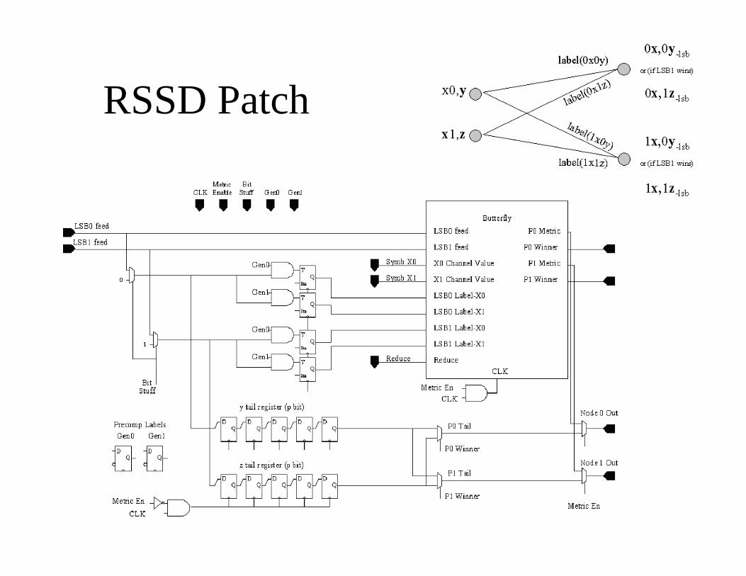
RSSD Patch

Interconnect Structure

Finished Design
3200 um X 3200 um63000 cells – 0.18um TSMC(1.6 V)
17 inputs (3.3,5V), 25 outputs (3.3 V)

Area and Cell Breakdown

Power Dissipation
Power Scaling vs Decode Strength
0.10
1.00
10.00
0 100 200 300 400 500 600
States
Pow
er (m
W)
Power in mWLinear (Ideal)

Chip Specifications• natural K=11 1024 state
• rate ½, generators (3346,2751)octal
• 3 bit soft decisions
• 8 levels of reduction (p=8 to 1) from 4 to 512 superstates
• state-parallel/bit-serial architecture
• signal gating to shut-off unused states
• pipelined path computation and traceback handling
• asynchronous dual-clocks for computation and traceback
•constant traceback depth of 64 symbols
•asynchronous IO interface with handshaking and bit counters
• variable frame sizes supported; from 1 to unlimited - bit counts roll at 2056
• reconfigurable interconnect in path computation units
• 8 separate token passing networks – 1 per level of decode strength
• independent pipelined traceback units for intermediate and final decode

Quantified Results
•Compute Requires
7+p+1 clock cycles/bit (from 16 to 8 cycles)critical path – 465 Mhz
– 58 Mbps down to 29 Mbps
• Decode Requires
5 + {2(5-p) if p<5; 1 otherwise} cycles/bit (from 6 to 37 cycles) critical path (RAM) - 166 Mhz
• Overall Data rate
7.9 Mbps (RSSD-0) to 4.5 Mbps (RSSD-8)
• Output latency of 3*64 = 192 symbol periods
• Average Power~ 1.54*RSSD-8= 1.3 mW @ 1 Mbps = 0.8 mA vs 81 mA for SC140 DSP