a344a344 sbs dala crrent onitor · a344a344 sbs dala crrent onitor ˜ ˜ general description the...
TRANSCRIPT
MAX34408/MAX34409 SMBus Dual/Quad Current Monitor
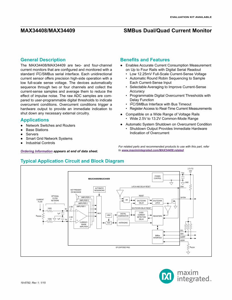
General DescriptionThe MAX34408/MAX34409 are two- and four-channel current monitors that are configured and monitored with a standard I2C/SMBus serial interface. Each unidirectional current sensor offers precision high-side operation with a low full-scale sense voltage. The devices automatically sequence through two or four channels and collect the current-sense samples and average them to reduce the effect of impulse noise. The raw ADC samples are com-pared to user-programmable digital thresholds to indicate overcurrent conditions. Overcurrent conditions trigger a hardware output to provide an immediate indication to shut down any necessary external circuitry.
Applications NetworkSwitchesandRouters BaseStations Servers SmartGridNetworkSystems IndustrialControls
Benefits and Features EnablesAccurateCurrentConsumptionMeasurement
onUptoFourRailswithDigitalSerialReadout• Low 12.25mV Full-Scale Current-Sense Voltage• AutomaticRoundRobinSequencingtoSample
Each Current-Sense Input• Selectable Averaging to Improve Current-Sense
Accuracy• Programmable Digital Overcurrent Thresholds with
Delay Function• I2C/SMBus Interface with Bus Timeout • RegisterAccesstoReal-TimeCurrentMeasurements
CompatibleonaWideRangeofVoltageRails• Wide2.5Vto13.2VCommon-ModeRange
AutomaticSystemShutdownonOvercurrentCondition• Shutdown Output Provides Immediate Hardware
Indication of Overcurrent
19-6792; Rev 1; 1/15
Ordering Information appears at end of data sheet.For related parts and recommended products to use with this part, refer to www.maximintegrated.com/MAX34408.related.
Typical Application Circuit and Block Diagram
EVALUATION KIT AVAILABLE
AMPLIFIER 2AMPLIFIER 3
AMPLIFIER 4
NOT PRESENTON MAX34408
2 OR4
2 OR4
AUTOMATICSEQUENCING
DIGITALCOMPARATORVREF
OR SHUTDOWNDELAY
RESET
LATCH AND DELAY RESET
SHUTDOWN DELAY RESET
SHUTDOWNLATCH
POWERCONTROL
GND
ENA
SHTDN
VDD
2.7V TO3.6V
OVER-CURRENT
DETECTIONDELAY
REGISTERS
SMBusINTERFACE
SCL
AVERAGING
EP (EXPOSED PAD)
MAX34408/MAX34409
CURRENT-SENSE
AMPLIFIER
MUX
AMPLIFIER 1
SDA
ALERT
ADDR
RADDR
ADC
IN-
IN+
1µF
1µF
100Ω
100ΩRSENSE
CURRENTFLOW
OPTIONALFILTER
NETWORK

MAX34408/MAX34409 SMBus Dual/Quad Current Monitor
www.maximintegrated.com Maxim Integrated 2
Recommended DC Operating Conditions(TA=-40°Cto+85°C.)(Notes2,3)
Electrical Characteristics(VIN+ = VIN-=12V,VSENSE=0V,VDD=2.7Vto3.6V,TA=-40°Cto+85°C,unlessotherwisenoted.TypicalvaluesareatVDD = 3.3V and TA=+25°C.)(Notes2,3)
Note 1: PackagethermalresistanceswereobtainedusingthemethoddescribedinJEDECspecificationJESD51-7,usingafour-layerboard.Fordetailedinformationonpackagethermalconsiderations,referto www.maximintegrated.com/thermal-tutorial.
VoltageRangeonVDDRelativetoGND ................-0.3V to +4VVoltageRangeonIN+,IN-RelativetoGND .........-0.3V to +16VVoltageRangeonAllOtherPins RelativetoGND... -0.3V to (VDD + 0.3V) (not to exceed +4V)
DifferentialInputVoltage,IN+toIN- ...................................±16V
Continuous Power Dissipation (TA = +70°C) 16-PinTQFN(derate25mW/°Cabove+70°C) .........2000mW
OperatingTemperatureRange ........................... -40°C to +85°CStorageTemperatureRange ............................ -55°C to +125°CSoldering Temperature (reflow) .......................................+260°CLeadTemperature(soldering,10s) .................................+300°C
Stresses beyond those listed under “Absolute Maximum Ratings” may cause permanent damage to the device. These are stress ratings only, and functional operation of the device at these or any other conditions beyond those indicated in the operational sections of the specifications is not implied. Exposure to absolute maximum rating conditions for extended periods may affect device reliability.
Package Thermal Characteristics(Note 1)TQFN Junction-to-AmbientThermalResistance(θJA)...........40°C/W Junction-to-CaseThermalResistance(θJC)..................6°C/W
Absolute Maximum Ratings
PARAMETER SYMBOL CONDITIONS MIN TYP MAX UNITSVDDOperatingVoltageRange VDD 2.7 3.6 V
InputLogic1:ENAPin VIH1VDD x
0.7VDD +
0.3 V
InputLogic0:ENAPin VIL1 -0.3 +0.3 x VDD V
Input Logic 1: SCL/SDA Pins VIH2 2.1 VDD + 0.3 V
Input Logic 0: SCL/SDA Pins VIL2 -0.3 +0.8 V
PARAMETER SYMBOL CONDITIONS MIN TYP MAX UNITSSupply Current IDD SMBus idle 830 µA
Current-Sense Common-Mode InputRange 2.5 13.2 V
InputBiasCurrent(IN+/IN-) Common-modevoltage=13.2V,INinputdifferential = 12.25mV 2 µA
ADCResolution 8 Bits
Per-Channel Current SampleRate 1 ksps
INInputFullScale 12.00 12.25 12.50 mV
ADCINL ±0.5 ±2 LSB
ADCDNL ±0.5 ±2 LSB
INInputOffset ±0.5 ±4 LSB
MAX34408/MAX34409 SMBus Dual/Quad Current Monitor
www.maximintegrated.com Maxim Integrated 3
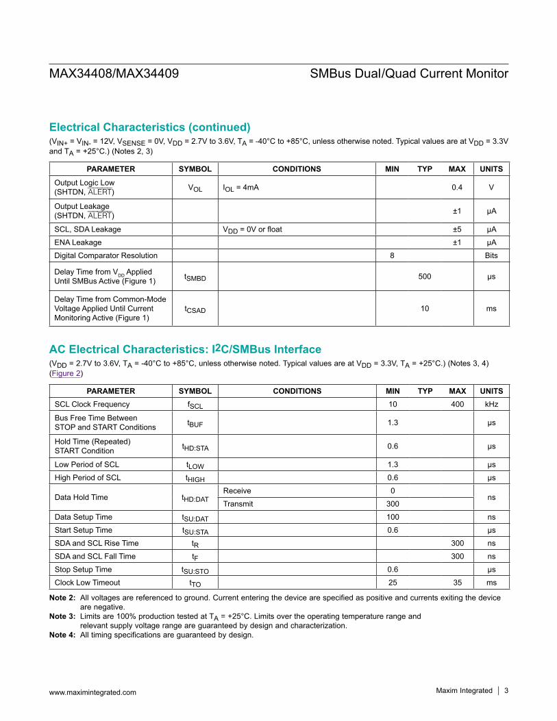
AC Electrical Characteristics: I2C/SMBus Interface(VDD=2.7Vto3.6V,TA=-40°Cto+85°C,unlessotherwisenoted.TypicalvaluesareatVDD=3.3V,TA=+25°C.)(Notes3,4) (Figure 2)
Electrical Characteristics (continued)(VIN+ = VIN-=12V,VSENSE=0V,VDD=2.7Vto3.6V,TA=-40°Cto+85°C,unlessotherwisenoted.TypicalvaluesareatVDD = 3.3V and TA=+25°C.)(Notes2,3)
Note 2: All voltages are referenced to ground. Current entering the device are specified as positive and currents exiting the device are negative.
Note 3: Limits are 100% production tested at TA = +25°C. Limits over the operating temperature range and relevant supply voltage range are guaranteed by design and characterization.
Note 4: All timing specifications are guaranteed by design.
PARAMETER SYMBOL CONDITIONS MIN TYP MAX UNITS
Output Logic Low(SHTDN,ALERT) VOL IOL = 4mA 0.4 V
OutputLeakage(SHTDN,ALERT) ±1 µA
SCL,SDALeakage VDD=0Vorfloat ±5 µA
ENALeakage ±1 µA
DigitalComparatorResolution 8 Bits
Delay Time from VDD Applied Until SMBus Active (Figure 1) tSMBD 500 µs
Delay Time from Common-Mode Voltage Applied Until Current Monitoring Active (Figure 1)
tCSAD 10 ms
PARAMETER SYMBOL CONDITIONS MIN TYP MAX UNITSSCLClockFrequency fSCL 10 400 kHz
Bus Free Time Between STOPandSTARTConditions tBUF 1.3 µs
HoldTime(Repeated) STARTCondition tHD:STA 0.6 µs
Low Period of SCL tLOW 1.3 µs
High Period of SCL tHIGH 0.6 µs
Data Hold Time tHD:DATReceive 0
nsTransmit 300
Data Setup Time tSU:DAT 100 ns
Start Setup Time tSU:STA 0.6 µs
SDAandSCLRiseTime tR 300 ns
SDA and SCL Fall Time tF 300 ns
Stop Setup Time tSU:STO 0.6 µs
ClockLowTimeout tTO 25 35 ms

MAX34408/MAX34409 SMBus Dual/Quad Current Monitor
www.maximintegrated.com Maxim Integrated 4
Timing Diagrams
Figure 1. Delay Timing
Figure 2. I2C/SMBus Timing
NOT ACTIVE
2.5V
VDD
SMBus
tSMBD
ACTIVE
NOT ACTIVECURRENTMONITORING
IN+
ACTIVE
2V
tCSAD
SCL
NOTE: TIMING IS REFERENCED TO VIL(MAX) AND VIH(MIN).
SDA
STOP START REPEATEDSTART
tBUF
tHD:STA
tHD:DAT tSU:DAT
tSU:STO
tHD:STA tSP
tSU:STAtHIGH
tR
tFtLOW

MAX34408/MAX34409 SMBus Dual/Quad Current Monitor
Maxim Integrated 5www.maximintegrated.com
(VDD = 3.3V and TA=+25°C,common-modevoltage=12.0V,unlessotherwisenoted.)Typical Operating Characteristics
0.60
0.65
0.70
0.75
0.80
2.6 2.8 3.0 3.2 3.4 3.6 3.8
I DD(m
A)
VDD (V)
SUPPLY CURRENT vs. SUPPLY VOLTAGE
toc01
0.60
0.65
0.70
0.75
0.80
-50 -30 -10 10 30 50 70 90
I DD(m
A)
TEMPERATURE (ºC)
SUPPLY CURRENTvs. TEMPERATURE
toc02
11.0
11.5
12.0
12.5
13.0
13.5
14.0
-50 -30 -10 10 30 50 70 90
FULL
SCA
LE (m
V)
TEMPERATURE (ºC)
IN INPUT FULL SCALEvs. TEMPERATURE
toc03
0
1
2
3
-50 -30 -10 10 30 50 70 90
OFFS
ET (L
SB)
TEMPERATURE (ºC)
IN INPUT OFFSETvs. TEMPERATURE
toc04
0
1
2
3
2 4 6 8 10 12 14
OFFS
ET (L
SB)
COMMON-MODE VOLTAGE (V)
IN INPUT OFFSETvs. COMMON-MODE VOLTAGE
toc05
0
100
200
300
400
500
600
700
0 5 10 15 20 25
VOL (
mV)
IOL (mA)
VOLvs. IOL
SHTDN, ALERT#, SDA PINS toc06
SHTDN
ALERT#
SDA
0
5
10
15
20
25
30
35
PERC
ENT
OF P
OPUL
ATIO
N (%
)
IN FULL SCALE (mV)
PERCENT OF POPULATION vs. IN FULL SCALE
toc07
0
5
10
15
20
25
30
PERC
ENT
OF P
OPUL
ATIO
N (%
)
OFFSET (LSB)
PERCENT OF POPULATIONvs. IN INPUT OFFSET
toc08
COMMON-MODE VOLTAGE = 2.5V

MAX34408/MAX34409 SMBus Dual/Quad Current Monitor
www.maximintegrated.com Maxim Integrated 6
Pin Description
Pin Configurations
PINNAME FUNCTION
MAX34408 MAX34409
1 1 IN1- ExternalSenseResistorLoad-SideConnectionforAmplifier1.Thispinshouldbe left open circuit if not needed.
2 2 SDA I2C/SMBus-Compatible Data Input/Output. Output is open drain.
3 3 SCL I2C/SMBus-CompatibleClockInput
4 4 IN2+ ExternalSenseResistorPower-SideConnectionforAmplifier2.Thispinshouldbeleft open circuit if not needed.
5 5 IN2- ExternalSenseResistorLoad-SideConnectionforAmplifier2.Thispinshouldbeleft open circuit if not needed.
6 6 ALERT I2C/SMBus Interrupt. Open-drain output.
7 7 GND GroundConnection
8,9,12,13 — N.C. NoConnection.Donotconnectanysignaltothispin.
10 10 SHTDNShutdown Output. Open-drain output. This output transitions to high impedance whenanyofthedigitalcomparatorthresholdsareexceededaslongastheENA pin is high.
11 11 ENASHTDNEnableInput.CMOSdigitalinput.ConnecttoGNDtoclearthelatchandunconditionallydeassert(forcelow)theSHTDNoutputandresettheshutdowndelay. Connect to VDDtoenablenormallatchoperationoftheSHTDNoutput.
14 14 ADDRI2C/SMBusAddressSelect.Ondevicepower-up,thedevicesamplesaresistortoground to determine the 7-bit serial bus address. See the Addressing section for details on which resistor values select which SMBus address.
15
16
14
13
6
5
7
SDA
IN2+
8
IN1-
ENA
N.C.
N.C.
1 2
ADDR
4
12 11 9
VDD
*EPIN1+
N.C.
GND
ALERT
IN2-+
SCL
SHTD
N
3
10
N.C.
16 TQFN(4mm x 4mm x 0.75mm)
MAX34408
TOP VIEW
*EXPOSED BACKSIDE PAD (EP)
15
16
14
13
6
5
7
SDA
IN2+
8
IN1-
ENA
IN3-
IN4+
1 2
ADDR
4
12 11 9
VDD
*EPIN1+
IN3+
GND
ALERT
IN2-+
SCL
SHTD
N
3
10
IN4-
MAX34409
MAX34408/MAX34409 SMBus Dual/Quad Current Monitor
www.maximintegrated.com Maxim Integrated 7
Pin Description (continued)
Detailed DescriptionThe MAX34408 and MAX34409 are two- and four-channel current monitors that are configured and monitored with a standard I2C/SMBus serial interface. Each unidirectional current sensor offers precision high-side operation with a low full-scale sense voltage. The devices automatically sequence through two or four channels and collect the current-sense samples and average them to reduce the effect of impulse noise. The raw ADC samples are com-pared to user-programmable digital thresholds to indicate overcurrent conditions. Overcurrent conditions trigger a hardware output to provide an immediate indication to shut down any necessary external circuitry.The devices provide an ALERT output signal. Host com-munications are conducted through a SMBus-compatible communications port.
SMBus OperationThe devices use the SMBus command/response for-mat as described in the System Management Bus Specification Version 2.0. The structure of the data flow between the host and the slave is shown for several dif-ferent types of transactions. Data is sent MSB first. The fixed slave address of the MAX34408 or MAX34409 is determined on device power-up by sampling the resistor connectedtotheADDRpin.SeetheAddressing section for details. On device power-up, the device defaults tothe STATUS command code (00h). If the host sends an invalidcommandcode,thedeviceNACKs(notacknowl-edge) the command code. If the host attempts to read the devicewithaninvalidcommandcode,allones(FFh)arereturned in the data byte.
PINNAME FUNCTION
MAX34408 MAX34409
15 15 VDDSupply Voltage for Comparators and Logic. A +2.7V to +3.6V supply. This pin shouldbedecoupledtoGNDwitha100nFceramiccapacitor.
16 16 IN1+ ExternalSenseResistorPower-SideConnectionforAmplifier1.Thispinshouldbeleft open circuit if not needed.
— 8 IN3+ ExternalSenseResistorPower-SideConnectionforAmplifier3.Thispinshouldbe left open circuit if not needed.
— 9 IN3- ExternalSenseResistorLoad-SideConnectionforAmplifier3.Thispinshouldbe left open circuit if not needed.
— 12 IN4+ ExternalSenseResistorPower-SideConnectionforAmplifier4.Thispinshouldbeleft open circuit if not needed.
— 13 IN4- ExternalSenseResistorLoad-SideConnectionforAmplifier4.Thispinshouldbeleft open circuit if not needed.
— — EP ExposedPad.Nointernalelectricalconnection.Canbeleftopencircuit.
MAX34408/MAX34409 SMBus Dual/Quad Current Monitor
www.maximintegrated.com Maxim Integrated 8
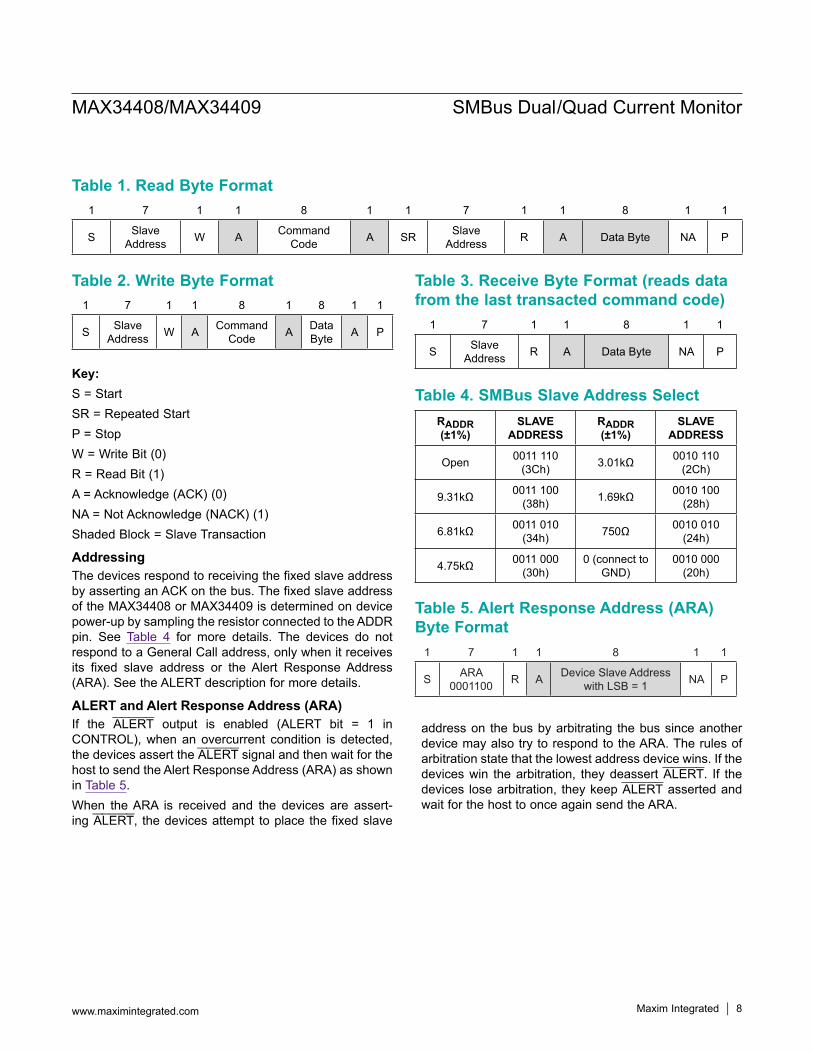
Key:S = StartSR=RepeatedStartP = StopW=WriteBit(0)R=ReadBit(1)A=Acknowledge(ACK)(0)NA=NotAcknowledge(NACK)(1)ShadedBlock=SlaveTransaction
AddressingThe devices respond to receiving the fixed slave address byassertinganACKonthebus.Thefixedslaveaddressof the MAX34408 or MAX34409 is determined on device power-upbysamplingtheresistorconnectedtotheADDRpin. See Table 4 for more details. The devices do not respondtoaGeneralCalladdress,onlywhenitreceivesits fixed slave address or the Alert Response Address(ARA).SeetheALERTdescriptionformoredetails.
ALERT and Alert Response Address (ARA)If the ALERT output is enabled (ALERT bit = 1 inCONTROL),whenanovercurrent condition is detected,the devices assert the ALERT signal and then wait for the hosttosendtheAlertResponseAddress(ARA)asshownin Table 5.When theARA is received and the devices are assert-ing ALERT, thedevicesattempt toplacethefixedslave
address on the bus by arbitrating the bus since another devicemayalsotrytorespondtotheARA.Therulesofarbitration state that the lowest address device wins. If the deviceswin thearbitration, theydeassertALERT. If the devices losearbitration, theykeepALERT asserted and waitforthehosttoonceagainsendtheARA.
Table 1. Read Byte Format
Table 2. Write Byte Format
Table 4. SMBus Slave Address Select
Table 5. Alert Response Address (ARA) Byte Format
Table 3. Receive Byte Format (reads data from the last transacted command code)
1 7 1 1 8 1 1 7 1 1 8 1 1
S SlaveAddress W A Command
Code A SR SlaveAddress R A Data Byte NA P
1 7 1 1 8 1 8 1 1
S SlaveAddress W A Command
Code A Data Byte A P 1 7 1 1 8 1 1
S SlaveAddress R A Data Byte NA P
RADDR (±1%)
SLAVE ADDRESS
RADDR (±1%)
SLAVE ADDRESS
Open 0011 110 (3Ch) 3.01kΩ 0010 110
(2Ch)
9.31kΩ 0011 100 (38h) 1.69kΩ 0010 100
(28h)
6.81kΩ 0011 010 (34h) 750Ω 0010 010
(24h)
4.75kΩ 0011 000 (30h)
0 (connect to GND)
0010 000 (20h)
1 7 1 1 8 1 1
S ARA0001100 R A Device Slave Address
with LSB = 1 NA P
MAX34408/MAX34409 SMBus Dual/Quad Current Monitor
www.maximintegrated.com Maxim Integrated 9
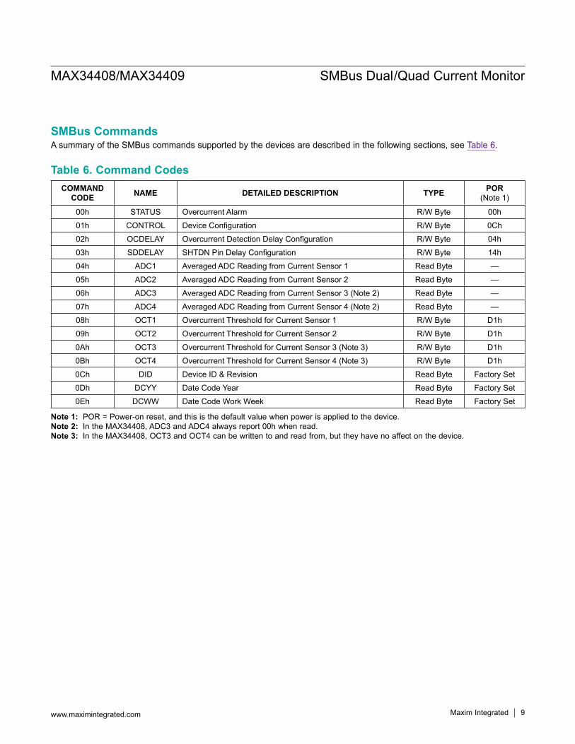
Table 6. Command Codes
SMBus CommandsAsummaryoftheSMBuscommandssupportedbythedevicesaredescribedinthefollowingsections,seeTable 6.
Note 1: POR=Power-onreset,andthisisthedefaultvaluewhenpowerisappliedtothedevice.Note 2: IntheMAX34408,ADC3andADC4alwaysreport00hwhenread.Note 3: IntheMAX34408,OCT3andOCT4canbewrittentoandreadfrom,buttheyhavenoaffectonthedevice.
COMMAND CODE NAME DETAILED DESCRIPTION TYPE POR
(Note1)
00h STATUS Overcurrent Alarm R/WByte 00h
01h CONTROL DeviceConfiguration R/WByte 0Ch
02h OCDELAY OvercurrentDetectionDelayConfiguration R/WByte 04h
03h SDDELAY SHTDNPinDelayConfiguration R/WByte 14h
04h ADC1 AveragedADCReadingfromCurrentSensor1 ReadByte —
05h ADC2 AveragedADCReadingfromCurrentSensor2 ReadByte —
06h ADC3 AveragedADCReadingfromCurrentSensor3(Note2) ReadByte —
07h ADC4 AveragedADCReadingfromCurrentSensor4(Note2) ReadByte —
08h OCT1 Overcurrent Threshold for Current Sensor 1 R/WByte D1h
09h OCT2 Overcurrent Threshold for Current Sensor 2 R/WByte D1h
0Ah OCT3 OvercurrentThresholdforCurrentSensor3(Note3) R/WByte D1h
0Bh OCT4 OvercurrentThresholdforCurrentSensor4(Note3) R/WByte D1h
0Ch DID DeviceID&Revision ReadByte Factory Set
0Dh DCYY Date Code Year ReadByte Factory Set
0Eh DCWW DateCodeWorkWeek ReadByte Factory Set
MAX34408/MAX34409 SMBus Dual/Quad Current Monitor
www.maximintegrated.com Maxim Integrated 10
Figure 3. OCn Status Bits Set/Clear Functionality and ALERT Assertion
Table 7. STATUS (00h)—R/W Byte
STATUS (00h)The STATUS command returns 1 byte of information with a summary of the fault conditions along with the real-time status oftheENAandSHTDNpins.TheSTATUSbytemessagecontentisdescribedinTable 7. See Figure 3 for STATUS bits 3:0 organization.
BIT BIT 7 BIT 6 BIT 5 BIT 4 BIT 3 BIT 2 BIT 1 BIT 0NAME NA NA ENA SHTDN OC4 OC3 OC2 OC1
POR 0 0 0 0 0 0 0 0
Note:BitpositionsmarkedasNAareNotAssignedandhavenomeaning.Thesebitscanbeeither0or1whenread.
BIT NAME DESCRIPTION
5 ENAThisbitreportsthereal-timestatusoftheENAinputpin.TheENApinissampledwhenSMBuscommunication is initiated. This bit has no affect on the ALERT output.Writinga0or1tothisbitposition has no affect on the device.
4 SHTDNThisbitreportsthereal-timestatusoftheSHTDNoutputpin.TheshutdownlatchissampledwhenSMBus communication is initiated. This bit has no affect on the ALERToutput.Writinga0or1tothisbit position has no affect on the device.
3:0OC4/OC3/ OC2/OC1
(MAX34409)
Thesebitsreflectthelatchedstatusoftheovercurrentthresholdsforeachcurrentsensor.TheOCD0toOCD3bitsconfiguredwiththeOCDELAYcommanddeterminethenumberofconsecutiveovercurrentthresholdexcursionsamplesthatarerequiredtosetthesebits.Onceset,thesebitsremainsetuntilwrittenwitha0.Oncetheyarecleared,theyarenotsetagainuntilthesensedcurrent has exceeded the threshold for the programmed delay time. The setting of any of these bits asserts the ALERTpiniftheALERTbitintheCONTROLcommandissettoaone.Readingor writing the STATUS command deasserts the ALERTpinifitisasserted.IntheMAX34408,bitpositions OC3 and OC4 are inactive.
1:0 OC2/OC1 (MAX34408)
CHANNEL 1 OVERCURRENT EVENT OVERCURRENT DELAY LATCH OC1
SET STATUS
CHANNEL 2 OVERCURRENT EVENT OVERCURRENT DELAY LATCH OC2
CHANNEL 3 OVERCURRENT EVENT OVERCURRENT DELAY LATCH OC3
CHANNEL 4
WRITE A 0 TO OCn BIT POSITIONIN STATUS COMMAND CODE
READ OR WRITE STATUS
ALERT RESPONSE ADDRESS (ARA)RECEIVED AND ARBITRATION WON
ALERT BIT IN CONTROL
CLEAR
OVERCURRENT EVENT OVERCURRENT DELAY LATCH OC4
OR
CLEAR
SET
LATCHOR
AND
ALERTOUTPUT

MAX34408/MAX34409 SMBus Dual/Quad Current Monitor
www.maximintegrated.com Maxim Integrated 11
CONTROL (01h)The CONTROL command configures the digital current-sensing averaging function. The CONTROL command alsodefinesifthedevicesrespondtotheAlertResponseAddress.TheCONTROLbytecommandisdescribedinTable 8.
Table 8. CONTROL (01h)—R/W ByteBIT BIT 7 BIT 6 BIT 5 BIT 4 BIT 3 BIT 2 BIT 1 BIT 0NAME NA NA NA NA ALERT AVG2 AVG1 AVG0
POR 0 0 0 0 1 1 0 0
Note:BitpositionsmarkedasNAareNotAssignedandhavenomeaning.Thesebitscanbeeither0or1whenread.
BIT NAME DESCRIPTION
3 ALERTIfthisbitiscleared,theALERToutputisdisabledandthedevicesdonotrespondtotheAlertResponseAddress.Ifthisbitisset,theALERTfunctionisenabledandthedevicesrespondtotheAlertResponseAddress.
2:0 AVG2/ AVG1/AVG0
Thesebitsconfigurethedigitalcurrent-sensingaveragingfunctionasshownbelow.
AVG2 AVG1 AVG0 SELECTED AVERAGING0 0 0 1 Sample (no averaging)
0 0 1 2 Samples
0 1 0 4 Samples
0 1 1 8 Samples
1 0 0 16 Samples (default)
1 0 1 32 Samples
1 1 0 64 Samples
1 1 1 128 Samples
MAX34408/MAX34409 SMBus Dual/Quad Current Monitor
www.maximintegrated.com Maxim Integrated 12
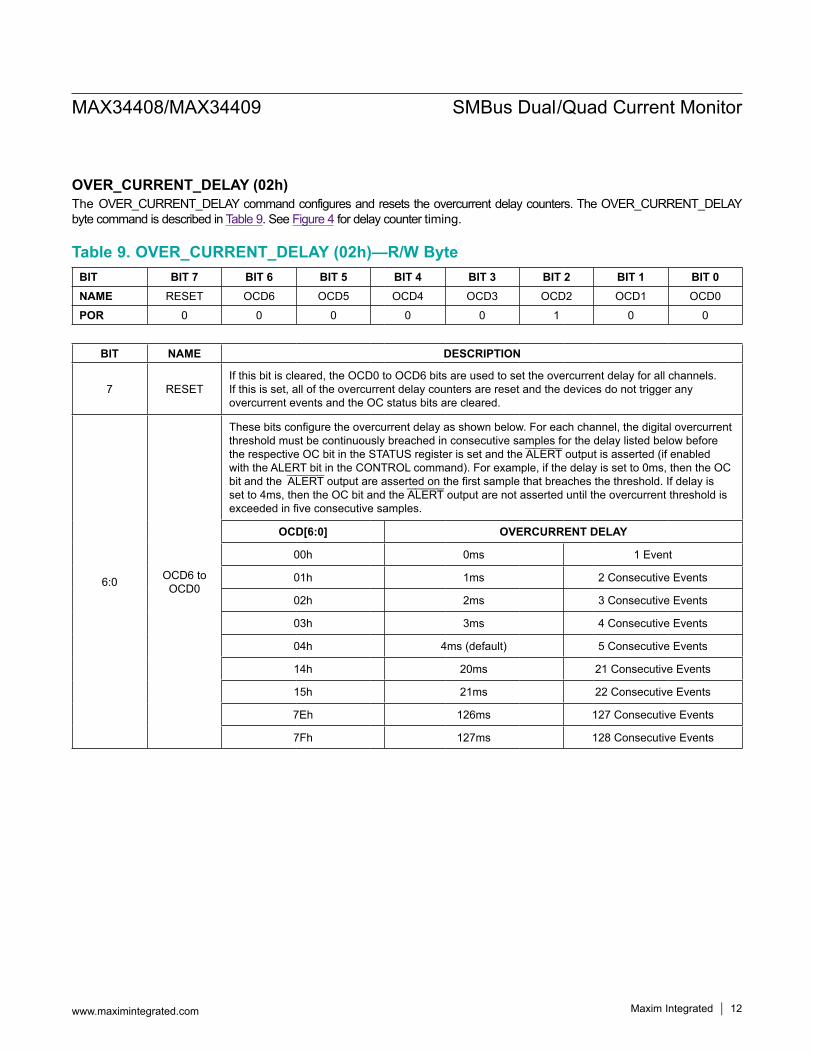
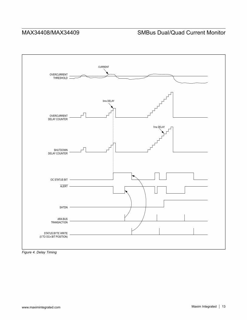
OVER_CURRENT_DELAY (02h)TheOVER_CURRENT_DELAYcommandconfiguresandresetstheovercurrentdelaycounters.TheOVER_CURRENT_DELAYbyte command is described in Table 9. See Figure 4 for delay counter timing.
Table 9. OVER_CURRENT_DELAY (02h)—R/W ByteBIT BIT 7 BIT 6 BIT 5 BIT 4 BIT 3 BIT 2 BIT 1 BIT 0NAME RESET OCD6 OCD5 OCD4 OCD3 OCD2 OCD1 OCD0
POR 0 0 0 0 0 1 0 0
BIT NAME DESCRIPTION
7 RESETIfthisbitiscleared,theOCD0toOCD6bitsareusedtosettheovercurrentdelayforallchannels.Ifthisisset,alloftheovercurrentdelaycountersareresetandthedevicesdonottriggeranyovercurrent events and the OC status bits are cleared.
6:0 OCD6 to OCD0
Thesebitsconfiguretheovercurrentdelayasshownbelow.Foreachchannel,thedigitalovercurrentthreshold must be continuously breached in consecutive samples for the delay listed below before the respective OC bit in the STATUS register is set and the ALERT output is asserted (if enabled withtheALERTbitintheCONTROLcommand).Forexample,ifthedelayissetto0ms,thentheOCbit and the ALERToutputareassertedonthefirstsamplethatbreachesthethreshold.Ifdelayissetto4ms,thentheOCbitandtheALERT output are not asserted until the overcurrent threshold is exceededinfiveconsecutivesamples.
OCD[6:0] OVERCURRENT DELAY
00h 0ms 1 Event
01h 1ms 2 Consecutive Events
02h 2ms 3 Consecutive Events
03h 3ms 4 Consecutive Events
04h 4ms (default) 5 Consecutive Events
14h 20ms 21 Consecutive Events
15h 21ms 22 Consecutive Events
7Eh 126ms 127 Consecutive Events
7Fh 127ms 128 Consecutive Events
MAX34408/MAX34409 SMBus Dual/Quad Current Monitor
www.maximintegrated.com Maxim Integrated 13
Figure 4. Delay Timing
CURRENT
OVERCURRENTTHRESHOLD
OVERCURRENTDELAY COUNTER
SHUTDOWNDELAY COUNTER
OC STATUS BIT
3ms DELAY
7ms DELAY
ALERT
SHTDN
ARA BUSTRANSACTION
STATUS BYTE WRITE(0 TO OCn BIT POSITION)
MAX34408/MAX34409 SMBus Dual/Quad Current Monitor
www.maximintegrated.com Maxim Integrated 14
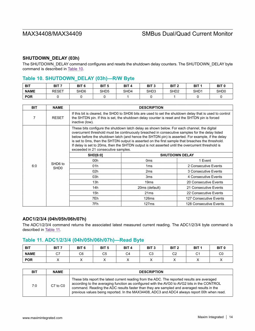
SHUTDOWN_DELAY (03h)TheSHUTDOWN_DELAYcommandconfiguresandresetstheshutdowndelaycounters.TheSHUTDOWN_DELAYbytecommand is described in Table 10.
ADC1/2/3/4 (04h/05h/06h/07h)The ADC1/2/3/4 command returns the associated latest measured current reading. The ADC1/2/3/4 byte command is described in Table 11.
Table 11. ADC1/2/3/4 (04h/05h/06h/07h)—Read Byte
Table 10. SHUTDOWN_DELAY (03h)—R/W Byte
BIT BIT 7 BIT 6 BIT 5 BIT 4 BIT 3 BIT 2 BIT 1 BIT 0NAME C7 C6 C5 C4 C3 C2 C1 C0
POR X X X X X X X X
BIT NAME DESCRIPTION
7:0 C7 to C0
These bits report the latest current reading from the ADC. The reported results are averaged accordingtotheaveragingfunctionasconfiguredwiththeAVG0toAVG2bitsintheCONTROLcommand.ReadingtheADCresultsfasterthantheyaresampledandaveragedresultsinthepreviousvaluesbeingreported.IntheMAX34408,ADC3andADC4alwaysreport00hwhenread.
BIT BIT 7 BIT 6 BIT 5 BIT 4 BIT 3 BIT 2 BIT 1 BIT 0NAME RESET SHD6 SHD5 SHD4 SHD3 SHD2 SHD1 SHD0POR 0 0 0 1 0 1 0 0
BIT NAME DESCRIPTION
7 RESETIfthisbitiscleared,theSHD0toSHD6bitsareusedtosettheshutdowndelaythatisusedtocontroltheSHTDNpin.Ifthisisset,theshutdowndelaycounterisresetandtheSHTDNpinisforcedinactive (low).
6:0 SHD6 to SHD0
Thesebitsconfiguretheshutdownlatchdelayasshownbelow.Foreachchannel,thedigitalovercurrent threshold must be continuously breached in consecutive samples for the delay listed belowbeforetheshutdownlatch(andhencetheSHTDNpin)isasserted.Forexample,ifthedelayissetto0ms,thentheSHTDNoutputisassertedonthefirstsamplethatbreachesthethreshold.Ifdelayissetto20ms,thentheSHTDNoutputisnotasserteduntiltheovercurrentthresholdisexceeded in 21 consecutive samples.
SHD[6:0] SHUTDOWN DELAY00h 0ms 1 Event01h 1ms 2 Consecutive Events02h 2ms 3 Consecutive Events03h 3ms 4 Consecutive Events13h 19ms 20 Consecutive Events14h 20ms (default) 21 Consecutive Events15h 21ms 22 Consecutive Events7Eh 126ms 127 Consecutive Events7Fh 127ms 128 Consecutive Events
MAX34408/MAX34409 SMBus Dual/Quad Current Monitor
www.maximintegrated.com Maxim Integrated 15
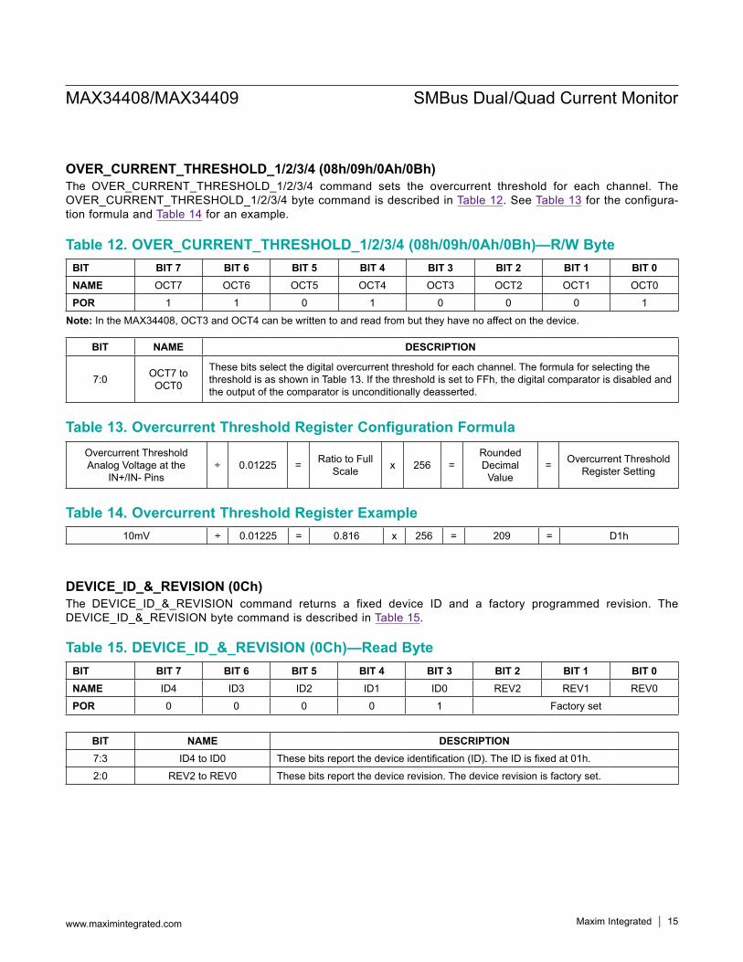
Table 12. OVER_CURRENT_THRESHOLD_1/2/3/4 (08h/09h/0Ah/0Bh)—R/W Byte
Table 13. Overcurrent Threshold Register Configuration Formula
Table 14. Overcurrent Threshold Register Example
OVER_CURRENT_THRESHOLD_1/2/3/4 (08h/09h/0Ah/0Bh)The OVER_CURRENT_THRESHOLD_1/2/3/4 command sets the overcurrent threshold for each channel. TheOVER_CURRENT_THRESHOLD_1/2/3/4bytecommandisdescribedinTable 12. See Table 13 for the configura-tion formula and Table 14 for an example.
DEVICE_ID_&_REVISION (0Ch)The DEVICE_ID_&_REVISION command returns a fixed device ID and a factory programmed revision. TheDEVICE_ID_&_REVISIONbytecommandisdescribedinTable 15.
Table 15. DEVICE_ID_&_REVISION (0Ch)—Read Byte
BIT BIT 7 BIT 6 BIT 5 BIT 4 BIT 3 BIT 2 BIT 1 BIT 0NAME OCT7 OCT6 OCT5 OCT4 OCT3 OCT2 OCT1 OCT0
POR 1 1 0 1 0 0 0 1
Note: IntheMAX34408,OCT3andOCT4canbewrittentoandreadfrombuttheyhavenoaffectonthedevice.
BIT NAME DESCRIPTION
7:0 OCT7 to OCT0
These bits select the digital overcurrent threshold for each channel. The formula for selecting the thresholdisasshowninTable13.IfthethresholdissettoFFh,thedigitalcomparatorisdisabledandthe output of the comparator is unconditionally deasserted.
Overcurrent Threshold Analog Voltage at the
IN+/IN-Pins÷ 0.01225 = RatiotoFull
Scale x 256 =RoundedDecimal
Value= Overcurrent Threshold
RegisterSetting
10mV ÷ 0.01225 = 0.816 x 256 = 209 = D1h
BIT BIT 7 BIT 6 BIT 5 BIT 4 BIT 3 BIT 2 BIT 1 BIT 0NAME ID4 ID3 ID2 ID1 ID0 REV2 REV1 REV0
POR 0 0 0 0 1 Factory set
BIT NAME DESCRIPTION7:3 ID4 to ID0 Thesebitsreportthedeviceidentification(ID).TheIDisfixedat01h.
2:0 REV2toREV0 These bits report the device revision. The device revision is factory set.

MAX34408/MAX34409 SMBus Dual/Quad Current Monitor
www.maximintegrated.com Maxim Integrated 16
Table 16. DATE_CODE_YEAR (0Dh)—Read Byte
Table 17. DATE_CODE_WORK_WEEK (0Eh)—Read Byte
DATE_CODE_YEAR (0Dh)TheDATE_CODE_YEARcommandreturnsafactoryprogrammeddatecode.TheDATE_CODE_YEARbytecommandis described in Table 16.
DATE_CODE_WORK_WEEK (0Eh)TheDATE_CODE_WORK_WEEKcommandreturnsafactory-programmeddatecode.TheDATE_CODE_WORK_WEEKbyte command is described in Table 17.
BIT BIT 7 BIT 6 BIT 5 BIT 4 BIT 3 BIT 2 BIT 1 BIT 0NAME 0 0 YY5 YY4 YY3 YY2 YY1 YY0
POR Factory Set
BIT NAME DESCRIPTION
5:0 YY5 to YY0
These bits report the last two decimal digits of the calendar year in which the device was tested. The year is reported as a binary decimal. Some examples are listed below. The range is valid until the year 2063.
YY[5:0] YEAR0Ch 20120Dh 201314h 2020
BIT BIT 7 BIT 6 BIT 5 BIT 4 BIT 3 BIT 2 BIT 1 BIT 0NAME 0 0 WW5 WW4 WW3 WW2 WW1 WW0
POR Factory Set
BIT NAME DESCRIPTION
5:0 WW5toWW0
Thesebitsreportthecalendarworkweekinwhichthedevicewastested.Theworkweekisreportedas a binary decimal. Some examples are listed below. 00h (0 decimal) and 36h (54 decimal) through 3Fh (63) are not valid.
WW[5:0] WORK WEEK06h 6
0Dh 13
2Bh 43
MAX34408/MAX34409 SMBus Dual/Quad Current Monitor
www.maximintegrated.com Maxim Integrated 17
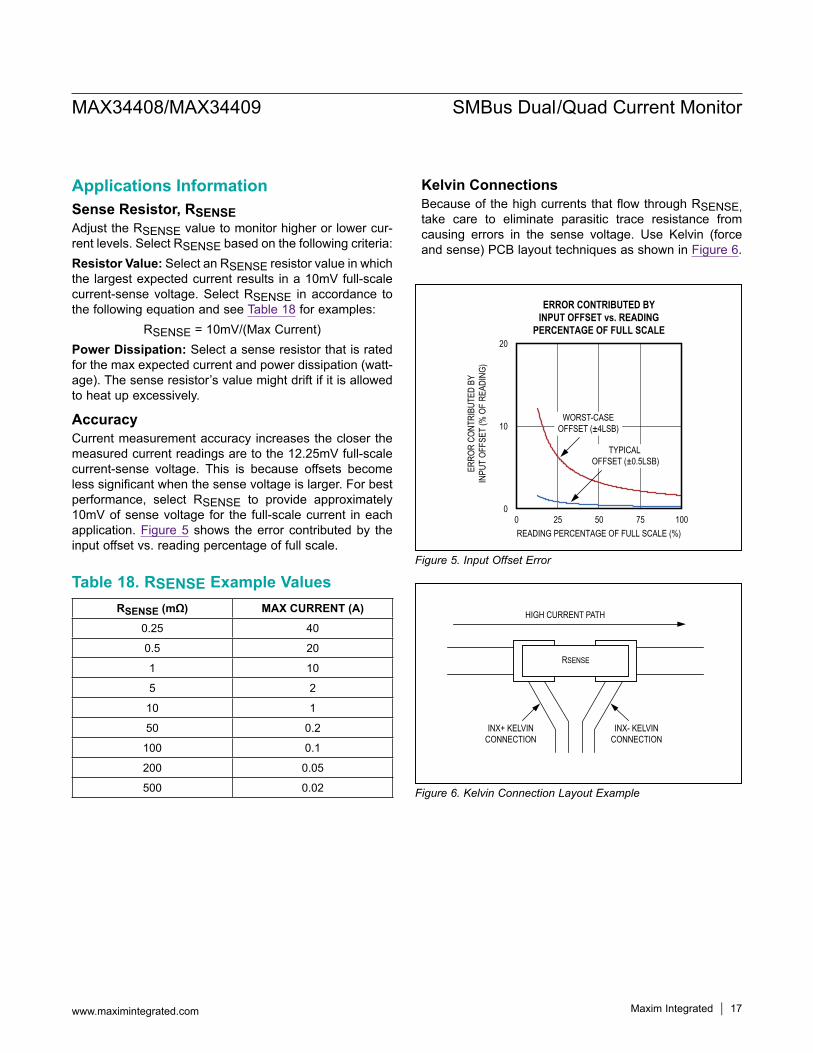
Applications InformationSense Resistor, RSENSEAdjusttheRSENSE value to monitor higher or lower cur-rentlevels.SelectRSENSE based on the following criteria:Resistor Value:SelectanRSENSE resistor value in which the largest expected current results in a 10mV full-scale current-sensevoltage.SelectRSENSE in accordance to the following equation and see Table 18 for examples:
RSENSE = 10mV/(Max Current)Power Dissipation: Select a sense resistor that is rated for the max expected current and power dissipation (watt-age). The sense resistor’s value might drift if it is allowed to heat up excessively.
AccuracyCurrent measurement accuracy increases the closer the measured current readings are to the 12.25mV full-scale current-sense voltage. This is because offsets become less significant when the sense voltage is larger. For best performance, select RSENSE to provide approximately 10mV of sense voltage for the full-scale current in each application. Figure 5 shows the error contributed by the input offset vs. reading percentage of full scale.
Kelvin ConnectionsBecauseofthehighcurrentsthatflowthroughRSENSE, take care to eliminate parasitic trace resistance fromcausing errors in the sense voltage. Use Kelvin (forceand sense) PCB layout techniques as shown in Figure 6.
Table 18. RSENSE Example ValuesFigure 5. Input Offset Error
Figure 6. Kelvin Connection Layout Example
RSENSE (mΩ) MAX CURRENT (A)
0.25 40
0.5 20
1 10
5 2
10 1
50 0.2
100 0.1
200 0.05
500 0.02
ERROR CONTRIBUTED BYINPUT OFFSET vs. READING
PERCENTAGE OF FULL SCALE
READING PERCENTAGE OF FULL SCALE (%)
ERRO
R CO
NTRI
BUTE
D BY
INPU
T OF
FSET
(% O
F RE
ADIN
G)
25 50 75
10
20
00 100
WORST-CASEOFFSET (±4LSB)
TYPICAL OFFSET (±0.5LSB)
RSENSE
HIGH CURRENT PATH
INX+ KELVINCONNECTION
INX- KELVINCONNECTION

MAX34408/MAX34409 SMBus Dual/Quad Current Monitor
www.maximintegrated.com Maxim Integrated 18
Optional Filter NetworkFor noisy environments, a simple lowpass filter canbe placed at the devices’ amplifier inputs as shown in Figure 7. The 100Ω resistor and 1µF capacitor providea 1.6kHz rolloff frequency.To achieve themost effectiveresults,usethefilterinconjunctionwiththedevice’sdigitalaveraging as described in the CONTROL (01h) section.
Layout ConsiderationsFornoisydigitalenvironments,theuseofamultilayerPCBwith separate ground and power-supply planes is recom-mended.Keepdigitalsignals faraway from thesensitiveanalog inputs. Unshielded long traces at the input termi-nals of the amplifier can degrade performance due to noise pickup.Theanalogdifferentialcurrent-sensetracesshouldbe routed close together to maximize common-mode rejec-tion.
Power-Supply DecouplingTo achieve the best results when using these devices,decouple the VDD power supply with a 0.1µF capacitor. Use a high-quality, ceramic, surface-mount capacitor ifpossible. Surface-mount components minimize lead induc-tance,which improvesperformance,andceramiccapaci-tors tend to have adequate high-frequency response for decoupling applications.
Figure 7. Filter Network
+Denotes a lead (Pb)-free/RoHS-compliant package.*EP = Exposed pad.
Ordering Information
Package InformationForthelatestpackageoutlineinformationandlandpatterns(foot-prints), go towww.maximintegrated.com/packages. Note thata“+”,“#”,or“-”inthepackagecodeindicatesRoHSstatusonly.Packagedrawingsmayshowadifferentsuffixcharacter,but thedrawingpertainstothepackageregardlessofRoHSstatus.
PART CONFIGURATION PIN-PACKAGEMAX34408ETE+ Dual 16TQFN-EP*
MAX34409ETE+ Quad 16TQFN-EP*
PACKAGETYPE
PACKAGECODE
OUTLINENO.
LANDPATTERN NO.
16TQFN-EP T1644+4 21-0139 90-0070
100Ω IN-
IN+
1µF
RESENSE
CURRENTFLOW
1µF
100Ω
OPTIONFILTER
NETWORK
Maxim Integrated cannot assume responsibility for use of any circuitry other than circuitry entirely embodied in a Maxim Integrated product. No circuit patent licenses are implied. Maxim Integrated reserves the right to change the circuitry and specifications without notice at any time. The parametric values (min and max limits) shown in the Electrical Characteristics table are guaranteed. Other parametric values quoted in this data sheet are provided for guidance.
Maxim Integrated and the Maxim Integrated logo are trademarks of Maxim Integrated Products, Inc.
MAX34408/MAX34409 SMBus Dual/Quad Current Monitor
© 2015 MaximIntegratedProducts,Inc. 19
Revision HistoryREVISION NUMBER
REVISION DATE DESCRIPTION PAGES
CHANGED0 9/13 Initial release —
1 1/15 Updated Benefits and Features section 1
For pricing, delivery, and ordering information, please contact Maxim Direct at 1-888-629-4642, or visit Maxim Integrated’s website at www.maximintegrated.com.