about omics group
DESCRIPTION
About Omics Group. - PowerPoint PPT PresentationTRANSCRIPT

About Omics Group
OMICS Group International through its Open Access Initiative is committed to make genuine and reliable contributions to the scientific community. OMICS Group hosts over 400 leading-edge peer reviewed Open Access Journals and organize over 300 International Conferences annually all over the world. OMICS Publishing Group journals have over 3 million readers and the fame and success of the same can be attributed to the strong editorial board which contains over 30000 eminent personalities that ensure a rapid, quality and quick review process.
About Omics Group conferences
• OMICS Group signed an agreement with more than 1000 International Societies to make healthcare information Open Access. OMICS Group Conferences make the perfect platform for global networking as it brings together renowned speakers and scientists across the globe to a most exciting and memorable scientific event filled with much enlightening interactive sessions, world class exhibitions and poster presentations
• Omics group has organised 500 conferences, workshops and national symposium across the major cities including SanFrancisco,Omaha,Orlado,Rayleigh,SantaClara,Chicago,Philadelphia,Unitedkingdom,Baltimore,SanAntanio,Dubai,Hyderabad,Bangaluru and Mumbai.

Manufacturing and performance of quantum cascade lasers for industrial applications
Mariano TroccoliDirector, Product Development
AdTech Optics Inc.

In-house capabilities at ATO
Device Fabricationburied-het process
for RT CW operation
Test and MountingC or CS open-mount, TO-3, HHL
Laser Designfull modeling of QCL devices with proprietary software
MOCVD Growth 2 reactors dedicated to QCLs production
FROM CONCEPT
TO PRODUCTION
12 YRS in business25 PPL on QCLs11,000 SQFTITAR compliant
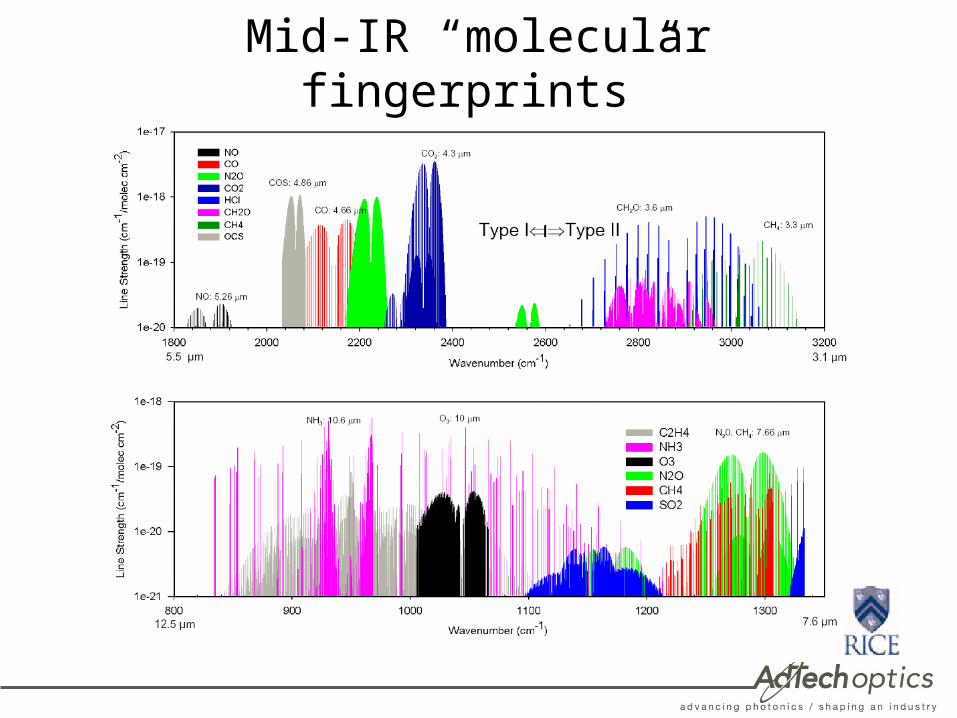
Mid-IR “molecular fingerprints”
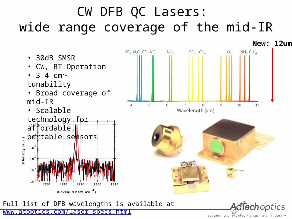
CW DFB QC Lasers: wide range coverage of the mid-IR
• 30dB SMSR• CW, RT Operation• 3-4 cm-1 tunability• Broad coverage of mid-IR• Scalable technology for affordable, portable sensors
Full list of DFB wavelengths is available at www.atoptics.com/laser_specs.html
10-5
10-4
10-3
10-2
10-1
100
1270 1280 1290 1300 1310
Wavenumbers (cm-1)
Inte
nsi
ty (
a.u
.)
New: 12um
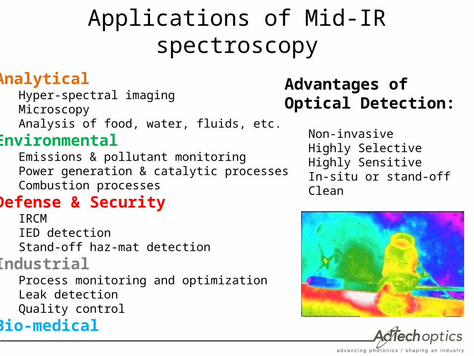
Applications of Mid-IR spectroscopy
AnalyticalHyper-spectral imagingMicroscopyAnalysis of food, water, fluids, etc.
EnvironmentalEmissions & pollutant monitoringPower generation & catalytic processesCombustion processes
Defense & SecurityIRCMIED detectionStand-off haz-mat detection
IndustrialProcess monitoring and optimizationLeak detectionQuality control
Bio-medical
Advantages of Optical Detection:
Non-invasiveHighly SelectiveHighly SensitiveIn-situ or stand-offClean
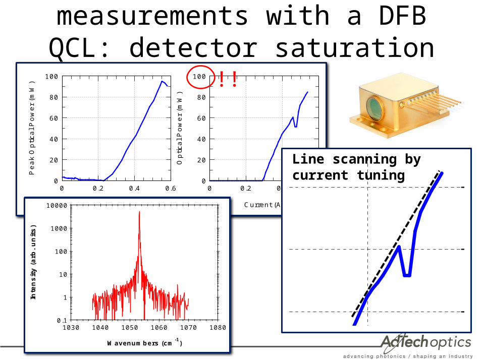
Direct Absorption measurements with a DFB QCL: detector saturation issues
0
20
40
60
80
100
0 0.2 0.4 0.6
Current (A)
Pe
ak
Op
tica
l Po
we
r (m
W)
0
20
40
60
80
100
0 0.2 0.4 0.6
Current (A)
Op
tica
l Po
we
r (m
W)
0
20
40
60
80
100
0 0.2 0.4 0.6
Current (A)
Op
tica
l Pow
er
(mW
)
Line scanning by current tuning
0.1
1
10
100
1000
10000
1030 1040 1050 1060 1070 1080
Wavenumbers (cm-1
)
Inte
ns
ity
(a
rb.
un
its
)
!!

Photo-Acoustic Sensing systems benefit from Hi Power QCLs
Sensor system
Multipass system QEPAS system
Cell volume 225 ml 7.5 ml
Response t ~1 minute Several seconds
Optical path 57 m (17 cm cell length) 1 cm
Laser power 1-10 mWs 120150 mW
BG noise Etalon fringe Optical/thermal noise
MDC (1s) CH4: 5.9 ppb, N2O: 2.6 ppb CH4: 13 ppb, N2O: 6ppb
ADTECHQCL
QEPAS CELL
OPTICS
GAS
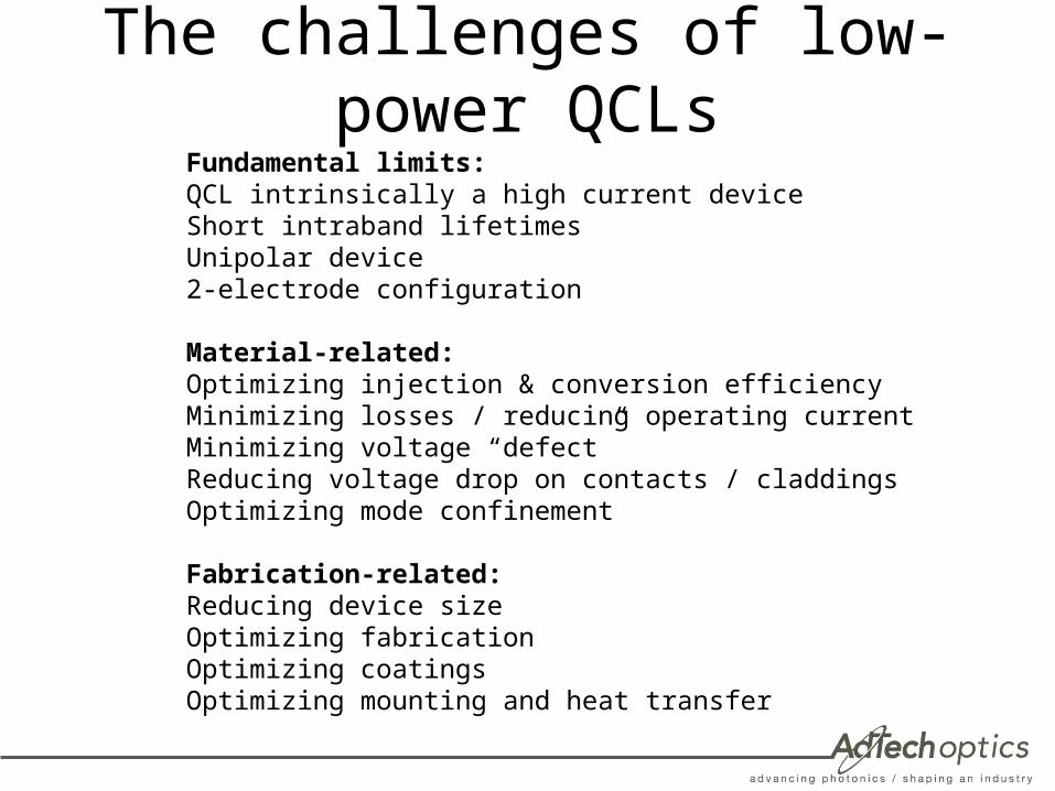
The challenges of low-power QCLsFundamental limits:QCL intrinsically a high current deviceShort intraband lifetimesUnipolar device2-electrode configuration
Material-related:Optimizing injection & conversion efficiencyMinimizing losses / reducing operating currentMinimizing voltage “defect”Reducing voltage drop on contacts / claddingsOptimizing mode confinement
Fabrication-related:Reducing device sizeOptimizing fabricationOptimizing coatingsOptimizing mounting and heat transfer
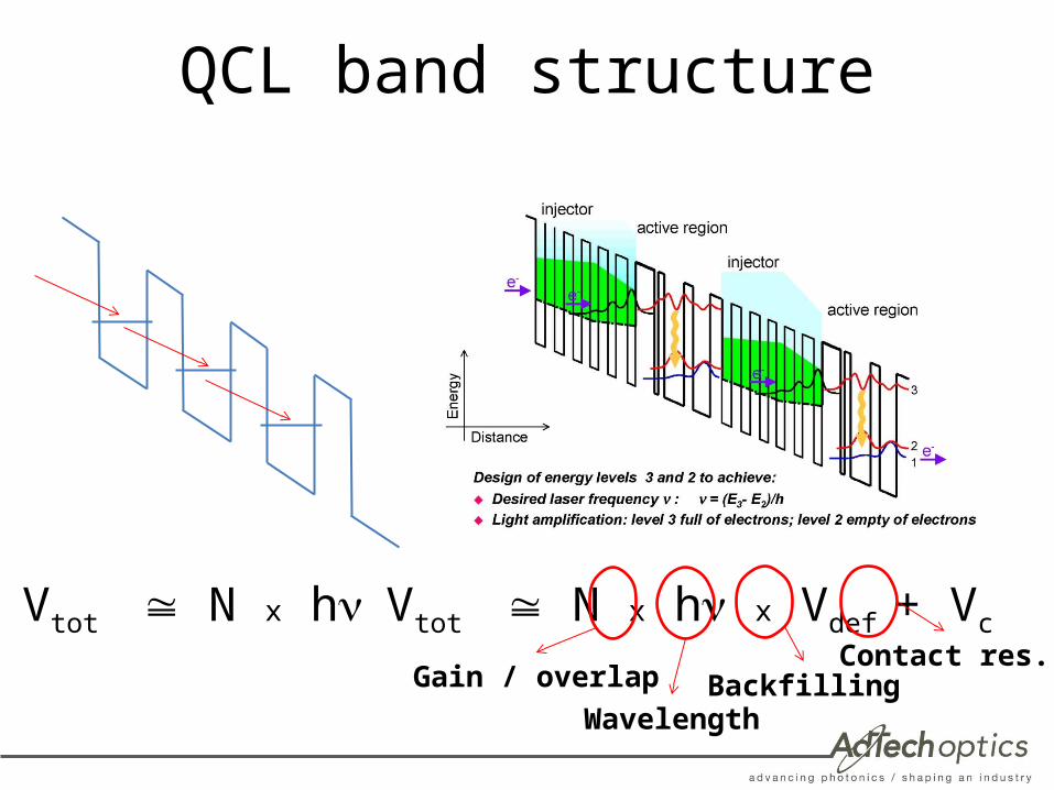
QCL band structure
Vtot N x h x Vdef + VcVtot N x hGain / overlap
WavelengthBackfilling
Contact res.
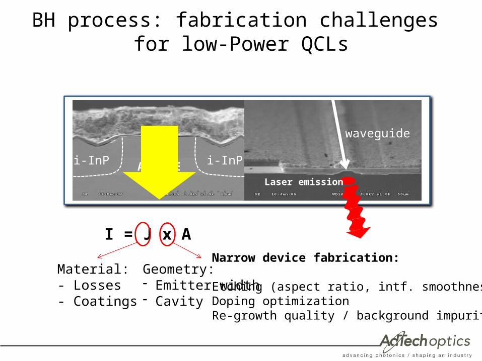
BH process: fabrication challenges for low-Power QCLs
ACTIVEi-InP i-InP
waveguide
Laser emission
Narrow device fabrication:
Etching (aspect ratio, intf. smoothness, …)Doping optimizationRe-growth quality / background impurities
I = J x A
Material:- Losses- Coatings
Geometry:- Emitter width- Cavity
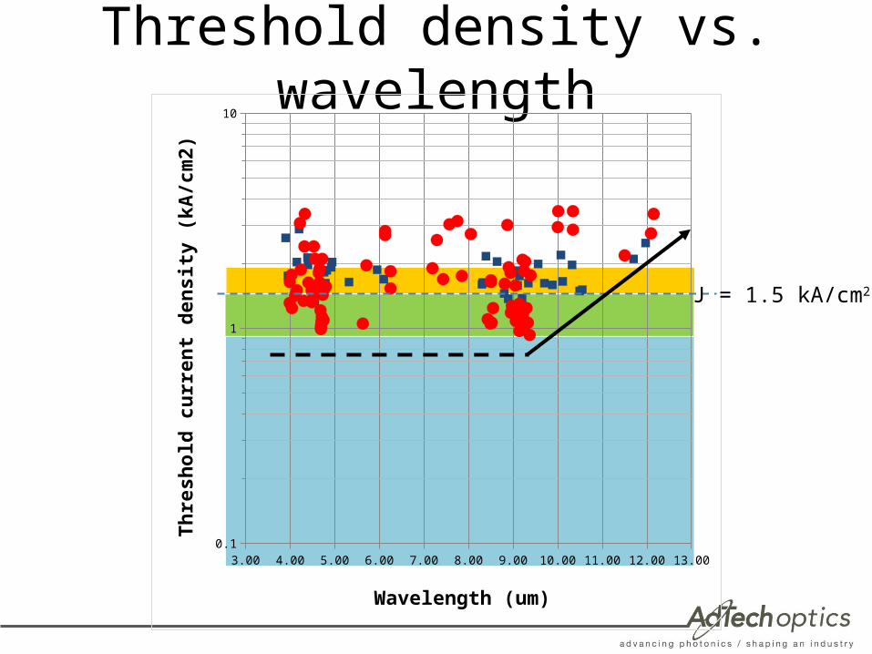
Threshold density vs. wavelength
3.00 4.00 5.00 6.00 7.00 8.00 9.00 10.00 11.00 12.00 13.000.1
1
10
Wavelength (um)
Thre
shol
d cu
rren
t den
sity
(kA/
cm2)
J = 1.5 kA/cm2

Jth vs. device width
2 3 4 5 6 7 8 90
0.5
1
1.5
2
2.5
Waveguide size (um)
Thre
shol
d cu
rren
t de
nsit
y (k
A/c
m2)
Device wavelength: 4.7um

Narrow BH devices @ 5um (pulsed operation, RT, no heat sinking)
(W)/10

Low-Consumption DFB QCL
0
20
40
60
80
0 0.05 0.10 0.15 0.20
15 C25 C35 C45 C
Current (A)O
ptic
al P
ower
(m
W)
= 4.5um ; Emitter Width= 3.7umPE
th = 0.8W ; PE(50mW) = 1.9W
4.57 4.58 4.59 4.60 4.61
15 C25 C35 C
Wavelength (m)
Inte
nsity
(ar
b. u
nits
)
50mW
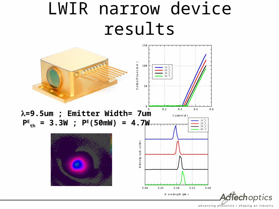
LWIR narrow device results
0
50
100
150
0 0.2 0.4 0.6 0.8
15 C25 C35 C45 C
Current (A)
Opt
ical
Pow
er (
mW
)
9.40 9.45 9.50 9.55 9.60
15 C25 C35 C45 C
Wavelength (m)
Inte
nsi
ty (
arb
. u
nits
)
=9.5um ; Emitter Width= 7umPE
th = 3.3W ; PE(50mW) = 4.7W

TO-3 DFBs for NH3 and CO2
0
200
400
600
0 0.4 0.8 1.2
Current (A)
Pe
ak
Op
tica
l Po
we
r (m
W)
4.33 4.34 4.35 4.36 4.37
15 C25 C35 C
Wavelength (m)In
ten
sity
(a
rb.
un
its)
0
100
200
300
0 0.4 0.8 1.2 1.6
Current (A)
Pe
ak
Op
tica
l Po
we
r (m
W)
0
50
100
150
0 0.25 0.50 0.75 1.00 1.25
Current (A)
Op
tica
l Po
we
r (m
W)
10.30 10.32 10.34 10.36 10.38
15 C25 C35 C
Wavelength (m)
Inte
nsity
(ar
b. u
nits
)
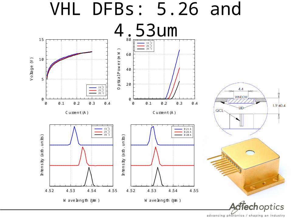
VHL DFBs: 5.26 and 4.53um
0
5
10
15
0 0.1 0.2 0.3 0.4
15 C25 C35 C
Current (A)
Vo
ltag
e (
V)
0
20
40
60
80
0 0.1 0.2 0.3 0.4
15 C25 C35 C
Current (A)O
ptic
al P
ow
er
(mW
)
4.52 4.53 4.54 4.55
15 C25 C35 C
Wavelength (m)
Inte
nsity
(ar
b. u
nits
)
4.52 4.53 4.54 4.55
0.21 A0.26 A0.30 A
Wavelength (m)
Inte
nsity
(ar
b. u
nits
)
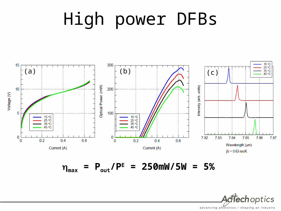
High power DFBs
(a) (b) (c)
max = Pout/PE = 250mW/5W = 5%
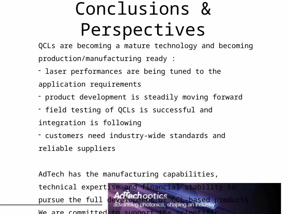
Conclusions & PerspectivesQCLs are becoming a mature technology and becoming
production/manufacturing ready :
- laser performances are being tuned to the application requirements
- product development is steadily moving forward
- field testing of QCLs is successful and integration is following
- customers need industry-wide standards and reliable suppliers
AdTech has the manufacturing capabilities, technical expertise and
financial stability to pursue the full development of QCL-based products.
We are committed to support the scientific community and our customers
throughout this process.
Acknowledgements
AdTech Optics Team
Jenyu Fan (fab operations)Xiaojun Wang (material development)Rommel Ceballos (processing)Hien Quach (testing)Ulisses Gamboa (packaging)Gene Lin (coating)Charles Luu (tech sales)Ed Ho (Finance)Mary Fong (CEO)
Support from DARPA, ONR, MDA

QCL ManufacturingDifferent stages of laser manufacturing process
Target specsDevice Design
RW device test
Material growthQuickturn fab
BH Fab
BH Test
Coating
MountingPackaging
Material release
Data compliance
BH control
Reviewand release
Specs verific. and approval-targets-tolerances-critical thresholds
Waferanalysis
Data compliance
User qualificationField Test
Coating inspection CW - full
test
Burn-in &Custom-test

QCL Manufacturing – quality controlMeasurements and technologies for manufacturing control and repeatability
0 200 400 600 800 1000 1200 1400 1600 1800PWPEmax
0 500 1000 1500 20000
200
400
600
800
1000
1200
Pmax
Sl1
0
1
2
3
4
5
6
WP
Em
ax
Typ,HR,CF,2,15,5,11.68,Q330,A1715B
Typ,HR,CF,2,15,5,10.97,Q369,A1646B
Typ,HR,CF,2,15,5,11.25,Q370,A1651A
Typ,HR,CF,2,15,5,10.66,Q445,A1651B
Typ,HR,CF,2,15,5,11.39,Q446,A2337D
Hi Pow
Hi Eff
30.4 30.6 30.8 31.0 31.2 31.4 31.6 31.8 32.0 32.2 32.4 32.6 32.8 33.0 33.2Omega-2Theta (°)
0.1
2
5
1
2
5
10
2
5
100
2
5
1000
2
5
10000
2
5
100000
Inte
nsity (
counts
)
Luminescence mapping
Xray-scattering mapping
Yields across processes
Let Us Meet Again
We welcome all to our future group conferences of Omics group international
Please visit:www.omicsgroup.com
www.Conferenceseries.com http://optics.conferenceseries.com/