abstract power and performance studies of the explicit multi
TRANSCRIPT

ABSTRACT
Title of dissertation: POWER AND PERFORMANCE STUDIES
OF THE EXPLICIT MULTI-THREADING (XMT)
ARCHITECTURE
Fuat Keceli, Doctor of Philosophy, 2011
Dissertation directed by: Professor Uzi Vishkin
Department of Electrical and
Computer Engineering
Power and thermal constraints gained critical importance in the design of micropro-
cessors over the past decade. Chipmakers failed to keep power at bay while sustaining the
performance growth of serial computers at the rate expected by consumers. As an alter-
native, they turned to fitting an increasing number of simpler cores on a single die. While
this is a step forward for relaxing the constraints, the issue of power is far from resolved
and it is joined by new challenges which we explain next.
As we move into the era of many-cores, processors consisting of 100s, even 1000s of
cores, single-task parallelism is the natural path for building faster general-purpose com-
puters. Alas, the introduction of parallelism to the mainstream general-purpose domain
brings another long elusive problem to focus: ease of parallel programming. The result
is the dual challenge where power efficiency and ease-of-programming are vital for the
prevalence of up and coming many-core architectures.
The observations above led to the lead goal of this dissertation: a first order valida-
tion of the claim that even under power/thermal constraints, ease-of-programming and com-

petitive performance need not be conflicting objectives for a massively-parallel general-
purpose processor. As our platform, we choose the eXplicit Multi-Threading (XMT) many-
core architecture for fine grained parallel programs developed at the University of Mary-
land. We hope that our findings will be a trailblazer for future commercial products.
XMT scales up to thousand or more lightweight cores and aims at improving single
task execution time while making the task for the programmer as easy as possible. Per-
formance advantages and ease-of-programming of XMT have been shown in a number
of publications, including a study that we present in this dissertation. Feasibility of the
hardware concept has been exhibited via FPGA and ASIC (per our partial involvement)
prototypes.
Our contributions target the study of power and thermal envelopes of an envisioned
1024-core XMT chip (XMT1024) under programs that exist in popular parallel benchmark
suites. First, we compare XMT against an area and power equivalent commercial high-end
many-core GPU. We demonstrate that XMT can provide an average speedup of 8.8x in ir-
regular parallel programs that are common and important in general purpose computing.
Even under the worst-case power estimation assumptions for XMT, average speedup is
only reduced by half. We further this study by experimentally evaluating the performance
advantages of Dynamic Thermal Management (DTM), when applied to XMT1024. DTM tech-
niques are frequently used in current single and multi-core processors, however until now
their effects on single-tasked many-cores have not been examined in detail. It is our pur-
pose to explore how existing techniques can be tailored for XMT to improve performance.
Performance improvements up to 46% over a generic global management technique has
been demonstrated. The insights we provide can guide designers of other similar many-
core architectures.
A significant infrastructure contribution of this dissertation is a highly configurable
cycle-accurate simulator, XMTSim. To our knowledge, XMTSim is currently the only
publicly-available shared-memory many-core simulator with extensive capabilities for es-
timating power and temperature, as well as evaluating dynamic power and thermal man-
agement algorithms. As a major component of the XMT programming toolchain, it is not
only used as the infrastructure in this work but also contributed to other publications and
dissertations.

POWER AND PERFORMANCE STUDIES OF THE EXPLICITMULTI-THREADING (XMT) ARCHITECTURE
by
Fuat Keceli
Dissertation submitted to the Faculty of the Graduate School of theUniversity of Maryland, College Park in partial fulfillment
of the requirements for the degree ofDoctor of Philosophy
2011
Advisory Committee:Professor Uzi Vishkin, Chair/AdvisorAssistant Professor Tali MoreshetAssociate Professor Manoj FranklinAssociate Professor Gang QuAssociate Professor William W. Pugh

c© Copyright by
Fuat Keceli
2011

To my loving mother, Gulbun, who never stopped believing in me.
Anneme.
ii

Acknowledgments
I would like to sincerely thank my advisors Dr. Uzi Vishkin and Dr. Tali Moreshet for
their guidance. It has been a long but rewarding journey through which they have always
been understanding and patient with me. Dr. Vishkin’s invaluable experiences, unique
insight and perseverance not only shaped my research, but also gave me an everlasting
perspective on defining and solving problems. Dr. Moreshet selflessly spent countless
hours in discussions with me, during which we cultivated the ideas that were collected in
this dissertation. Her advice as a mentor and a friend kept me focused and taught me how
to convey ideas clearly. It was a privilege to have both as my advisors.
I am indebted to the past and present members of the XMT team, especially my good
friends George C. Caragea and Alexandros Tzannes with whom I worked closely and puz-
zled over many problems. James Edwards’ collaboration and feedback was often crucial.
Aydin Balkan, Xingzhi Wen and Michael Horak were exceptional colleagues during their
time in the team. I would not have made it to the finish line without their help.
It was the sympathetic ear of many friends that kept me sane through the course of
difficult years. They have helped me deal with the setbacks along the way, push through
the pain of my father’s long illness and gave me a space where I can let off steam. Thank
you (in no particular order), Apoorva Prasad, Thanos Chrysis, Harsh Dhundia, Nimi Dvir,
Orkan Dere, Bulent Boyaci, and everybody else that I may have inadvertently left out.
Apoorva Prasad deserves a special mention, for he took the time to proofread most of this
dissertation during his brief visit from overseas.
Finally and most importantly, I would like express my heart-felt gratitude to my family.
I am lucky that my mother Gulbun and my brother Alp were, are, and always will be with
me. Alas, my father Ismail, who was the first engineer that I knew and a very good one,
passed away in 2009; he lives in our memories and our hearts. I would not be the person
that I am today without their unwavering support, encouragement, and love. I owe many
thanks to Tina Peterson for being my family away from home, for her continuous support
and concern. Lastly, I will always remember my grandfather, Muzaffer Tuncel, as the
person who planted the seeds of scientific curiosity in me.
iii

Table of Contents
List of Tables ix
List of Figures x
List of Abbreviations xiii
1 Introduction 1
2 Background on Power/Temperature Estimation and Management 5
2.1 Sources of Power Dissipation in Digital Processors . . . . . . . . . . . . . . . 5
2.2 Dynamic Power Consumption . . . . . . . . . . . . . . . . . . . . . . . . . . 6
2.2.1 Clock Gating . . . . . . . . . . . . . . . . . . . . . . . . . . . . . . . . 6
2.2.2 Estimation of of Dynamic Power in Simulation . . . . . . . . . . . . . 7
2.3 Leakage Power Consumption . . . . . . . . . . . . . . . . . . . . . . . . . . . 9
2.3.1 Management of Leakage Power . . . . . . . . . . . . . . . . . . . . . 10
2.3.2 Estimation of of Leakage Power in Simulation . . . . . . . . . . . . . 11
2.4 Power Consumption in On-Chip Memories . . . . . . . . . . . . . . . . . . . 12
2.5 Power and Clock Speed Trade-offs . . . . . . . . . . . . . . . . . . . . . . . . 12
2.6 Dynamic Scaling of Voltage and Frequency . . . . . . . . . . . . . . . . . . . 14
2.7 Technology Scaling Trends . . . . . . . . . . . . . . . . . . . . . . . . . . . . . 16
2.8 Thermal Modeling and Design . . . . . . . . . . . . . . . . . . . . . . . . . . 18
2.9 Power and Thermal Constraints in Recent Processors . . . . . . . . . . . . . 21
2.10 Tools for Area, Power and Temperature Estimation . . . . . . . . . . . . . . 22
3 The Explicit Multi-Threading (XMT) Platform 24
3.1 The XMT Architecture . . . . . . . . . . . . . . . . . . . . . . . . . . . . . . . 25
3.1.1 Memory Organization . . . . . . . . . . . . . . . . . . . . . . . . . . . 26
3.1.2 The Mesh-of-Trees Interconnect (MoT-ICN) . . . . . . . . . . . . . . . 26
3.2 Programming of XMT . . . . . . . . . . . . . . . . . . . . . . . . . . . . . . . 28
3.2.1 The PRAM Model . . . . . . . . . . . . . . . . . . . . . . . . . . . . . 28
3.2.2 XMTC – Enhanced C Programming for XMT . . . . . . . . . . . . . . 29
3.2.3 The Prefix-Sum Operation . . . . . . . . . . . . . . . . . . . . . . . . . 30
iv

3.2.4 Example Program . . . . . . . . . . . . . . . . . . . . . . . . . . . . . . 31
3.2.5 Independence-of-Order and No-Busy-Wait . . . . . . . . . . . . . . . 31
3.2.6 Ease-of-Programming . . . . . . . . . . . . . . . . . . . . . . . . . . . 32
3.3 Thread Scheduling in XMT . . . . . . . . . . . . . . . . . . . . . . . . . . . . 34
3.4 Performance Advantages . . . . . . . . . . . . . . . . . . . . . . . . . . . . . 36
3.5 Power Efficiency of XMT and Design for Power Management . . . . . . . . 36
3.5.1 Suitability of the Programming Model . . . . . . . . . . . . . . . . . . 37
3.5.2 Re-designing Thread Scheduling for Power . . . . . . . . . . . . . . . 37
3.5.3 Low Power States for Clusters . . . . . . . . . . . . . . . . . . . . . . 40
3.5.4 Power Management of the Synchronous MoT-ICN . . . . . . . . . . . 41
3.5.5 Power Management of Shared Caches – Dynamic Cache Resizing . . 42
4 XMTSim – The Cycle-Accurate Simulator of the XMT Architecture 44
4.1 Overview of XMTSim . . . . . . . . . . . . . . . . . . . . . . . . . . . . . . . . 45
4.2 Simulation Statistics and Runtime Control . . . . . . . . . . . . . . . . . . . . 48
4.3 Details of Cycle-Accurate Simulation . . . . . . . . . . . . . . . . . . . . . . . 49
4.3.1 Discrete-Event Simulation . . . . . . . . . . . . . . . . . . . . . . . . . 49
4.3.2 Concurrent Communication of Data Between Components . . . . . . 52
4.3.3 Optimizing the DE Simulation Performance . . . . . . . . . . . . . . 54
4.3.4 Simulation Speed . . . . . . . . . . . . . . . . . . . . . . . . . . . . . . 56
4.4 Cycle Verification Against the FPGA Prototype . . . . . . . . . . . . . . . . . 58
4.5 Power and Temperature Estimation in XMTSim . . . . . . . . . . . . . . . . 61
4.5.1 The Power Model . . . . . . . . . . . . . . . . . . . . . . . . . . . . . . 62
4.6 Dynamic Power and Thermal Management in XMTSim . . . . . . . . . . . . 65
4.7 Other Features . . . . . . . . . . . . . . . . . . . . . . . . . . . . . . . . . . . . 65
4.8 Features under Development . . . . . . . . . . . . . . . . . . . . . . . . . . . 66
4.9 Related Work . . . . . . . . . . . . . . . . . . . . . . . . . . . . . . . . . . . . 67
5 Enabling Meaningful Comparison of XMT with Contemporary Platforms 68
5.1 The Compared Architecture – NVIDIA Tesla . . . . . . . . . . . . . . . . . . 69
5.1.1 Tesla/CUDA Framework . . . . . . . . . . . . . . . . . . . . . . . . . 70
5.1.2 Comparison of the XMT and the Tesla Architectures . . . . . . . . . . 71
5.2 Silicon Area Feasibility of 1024-TCU XMT . . . . . . . . . . . . . . . . . . . . 74
v

5.2.1 ASIC Synthesis of a 64-TCU Prototype . . . . . . . . . . . . . . . . . . 74
5.2.2 Silicon Area Estimation for XMT1024 . . . . . . . . . . . . . . . . . . 74
5.3 Benchmarks . . . . . . . . . . . . . . . . . . . . . . . . . . . . . . . . . . . . . 78
5.4 Performance Comparison of XMT1024 and the GTX280 . . . . . . . . . . . . 82
5.5 Conclusions . . . . . . . . . . . . . . . . . . . . . . . . . . . . . . . . . . . . . 83
6 Power/Performance Comparison of XMT1024 and GTX280 84
6.1 Power Model Parameters for XMT1024 . . . . . . . . . . . . . . . . . . . . . 84
6.2 First Order Power Comparison of XMT1024 and GTX280 . . . . . . . . . . . 86
6.3 GPU Measurements and Simulation Results . . . . . . . . . . . . . . . . . . . 87
6.3.1 Benchmarks . . . . . . . . . . . . . . . . . . . . . . . . . . . . . . . . . 88
6.3.2 GPU Measurements . . . . . . . . . . . . . . . . . . . . . . . . . . . . 88
6.3.3 XMT Simulations and Comparison with GTX280 . . . . . . . . . . . . 89
6.4 Sensitivity of Results to Power Model Errors . . . . . . . . . . . . . . . . . . 91
6.4.1 Clusters, Caches and Memory Controllers . . . . . . . . . . . . . . . 91
6.4.2 Interconnection Network . . . . . . . . . . . . . . . . . . . . . . . . . 93
6.4.3 Putting it together . . . . . . . . . . . . . . . . . . . . . . . . . . . . . 95
6.5 Discussion of Detailed Data . . . . . . . . . . . . . . . . . . . . . . . . . . . . 95
6.5.1 Sensitivity to ICN and Cluster Clock Frequencies . . . . . . . . . . . 95
6.5.2 Power Breakdown for Different Cases . . . . . . . . . . . . . . . . . . 97
7 Dynamic Thermal Management of the XMT1024 Processor 99
7.1 Thermal Simulation Setup . . . . . . . . . . . . . . . . . . . . . . . . . . . . . 100
7.2 Benchmarks . . . . . . . . . . . . . . . . . . . . . . . . . . . . . . . . . . . . . 102
7.2.1 Benchmark Characterization . . . . . . . . . . . . . . . . . . . . . . . 103
7.3 Thermally Efficient Floorplan for XMT1024 . . . . . . . . . . . . . . . . . . . 108
7.3.1 Evaluation of Floorplans without DTM . . . . . . . . . . . . . . . . . 112
7.4 DTM Background . . . . . . . . . . . . . . . . . . . . . . . . . . . . . . . . . . 115
7.4.1 Control of Temperature via PID Controllers . . . . . . . . . . . . . . . 116
7.5 DTM Algorithms and Evaluation . . . . . . . . . . . . . . . . . . . . . . . . . 118
7.5.1 Analysis of DTM Results . . . . . . . . . . . . . . . . . . . . . . . . . 119
7.5.2 CG-DDVFS . . . . . . . . . . . . . . . . . . . . . . . . . . . . . . . . . 123
7.5.3 FG-DDVFS . . . . . . . . . . . . . . . . . . . . . . . . . . . . . . . . . 124
vi

7.5.4 LP-DDVFS . . . . . . . . . . . . . . . . . . . . . . . . . . . . . . . . . . 124
7.5.5 Effect of floorplan . . . . . . . . . . . . . . . . . . . . . . . . . . . . . . 125
7.6 Future Work . . . . . . . . . . . . . . . . . . . . . . . . . . . . . . . . . . . . . 125
7.7 Related Work . . . . . . . . . . . . . . . . . . . . . . . . . . . . . . . . . . . . 127
8 Conclusion 129
A Basics of Digital CMOS Logic 131
A.1 The MOSFET . . . . . . . . . . . . . . . . . . . . . . . . . . . . . . . . . . . . 131
A.2 A Simple CMOS Logic Gate: The Inverter . . . . . . . . . . . . . . . . . . . . 131
A.3 Dynamic Power . . . . . . . . . . . . . . . . . . . . . . . . . . . . . . . . . . . 133
A.3.1 Switching Power . . . . . . . . . . . . . . . . . . . . . . . . . . . . . . 134
A.3.2 Short Circuit Power . . . . . . . . . . . . . . . . . . . . . . . . . . . . 135
A.4 Leakage Power . . . . . . . . . . . . . . . . . . . . . . . . . . . . . . . . . . . 135
A.4.1 Subthreshold Leakage . . . . . . . . . . . . . . . . . . . . . . . . . . . 136
A.4.2 Leakage due to Gate Oxide Scaling . . . . . . . . . . . . . . . . . . . . 139
A.4.2.1 Junction Leakage . . . . . . . . . . . . . . . . . . . . . . . . . 139
B Extended XMTSim Documentation 140
B.1 General Information and Installation . . . . . . . . . . . . . . . . . . . . . . . 140
B.1.1 Dependencies and install . . . . . . . . . . . . . . . . . . . . . . . . . 140
B.2 XMTSim Manual . . . . . . . . . . . . . . . . . . . . . . . . . . . . . . . . . . 142
B.3 XMTSim Configuration Options . . . . . . . . . . . . . . . . . . . . . . . . . 149
C HotSpotJ 157
C.1 Installation . . . . . . . . . . . . . . . . . . . . . . . . . . . . . . . . . . . . . . 157
C.1.1 Software Dependencies . . . . . . . . . . . . . . . . . . . . . . . . . . 157
C.1.2 Building the Binaries . . . . . . . . . . . . . . . . . . . . . . . . . . . . 158
C.2 Limitations . . . . . . . . . . . . . . . . . . . . . . . . . . . . . . . . . . . . . . 159
C.3 Summary of Features . . . . . . . . . . . . . . . . . . . . . . . . . . . . . . . . 160
C.4 HotSpotJ Terminology . . . . . . . . . . . . . . . . . . . . . . . . . . . . . . . 161
C.4.1 Creating/Running Experiments and Displaying Results . . . . . . . 163
C.5 Tutorial – Floorplan of a 21x21 many-core processor . . . . . . . . . . . . . . 164
C.5.1 The Java code for the 21x21 Floorplan . . . . . . . . . . . . . . . . . . 164
vii

C.6 HotSpotJ Command Line Options . . . . . . . . . . . . . . . . . . . . . . . . 166
D Alternative Floorplans for XMT1024 169
Bibliography 171
viii

List of Tables
2.1 A survey of thermal design powers. . . . . . . . . . . . . . . . . . . . . . . . 22
4.1 Advantages and disadvantages of DE vs. DT simulation. . . . . . . . . . . . 52
4.2 Simulated throughputs of XMTSim. . . . . . . . . . . . . . . . . . . . . . . . 58
4.3 The configuration of XMTSim that is used in validation against Paraleap. . . 58
4.4 Microbenchmarks used in cycle verification . . . . . . . . . . . . . . . . . . . 60
5.1 Implementation differences between XMT and Tesla. . . . . . . . . . . . . . 73
5.2 Hardware specifications of the GTX280 and the simulated XMT configuration. 76
5.3 The detailed specifications of XMT1024. . . . . . . . . . . . . . . . . . . . . . 76
5.4 The area estimation for a 65 nm XMT1024 chip. . . . . . . . . . . . . . . . . . 77
5.5 Benchmark properties in XMTC and CUDA. . . . . . . . . . . . . . . . . . . 81
5.6 Percentage of time XMT spent on various types of instructions. . . . . . . . 83
6.1 Power model parameters for XMT1024. . . . . . . . . . . . . . . . . . . . . . 85
6.2 Benchmarks and results of experiments. . . . . . . . . . . . . . . . . . . . . . 88
7.1 Benchmark properties . . . . . . . . . . . . . . . . . . . . . . . . . . . . . . . 107
7.2 The baseline clock frequencies . . . . . . . . . . . . . . . . . . . . . . . . . . . 119
C.1 Specifications of the HotSpotJ test system. . . . . . . . . . . . . . . . . . . . . 158
ix

List of Figures
2.1 Addition of power gating to a logic circuit. . . . . . . . . . . . . . . . . . . . 10
2.2 Demonstration of dynamic energy savings with DVFS. . . . . . . . . . . . . 14
2.3 VF curve for Pentium M765 and AMD Athlon 4000+ processors. . . . . . . . 16
2.4 Modeling of temperature and heat analogous to RC circuits. . . . . . . . . . 19
2.5 Side view of a chip with packaging and heat sink, and its simplified RC model. 20
2.6 Thermal image of a single core of IBM PowerPC 970 processor. . . . . . . . . 21
3.1 Overview of the XMT architecture. . . . . . . . . . . . . . . . . . . . . . . . . 25
3.2 Bit fields in an XMT memory address. . . . . . . . . . . . . . . . . . . . . . . 26
3.3 The Mesh-of-Trees interconnect. . . . . . . . . . . . . . . . . . . . . . . . . . . 27
3.4 Building blocks of MoT-ICN. . . . . . . . . . . . . . . . . . . . . . . . . . . . 27
3.5 XMTC programming. . . . . . . . . . . . . . . . . . . . . . . . . . . . . . . . . 32
3.6 Flowchart for starting and distributing threads. . . . . . . . . . . . . . . . . . 33
3.7 Execution of a parallel section with 7 threads on a 4 TCU XMT system. . . . 35
3.8 Sleep-wake mechanism for thread ID check in TCUs. . . . . . . . . . . . . . 38
3.9 Addition of thread gating to thread scheduling of XMT. . . . . . . . . . . . . 39
3.10 The state diagram for the activity state of TCUs. . . . . . . . . . . . . . . . . 40
3.11 Modification of address bit-fields for cache resizing. . . . . . . . . . . . . . . 42
4.1 XMT overview from the perspective of XMTSim software structure. . . . . . 46
4.2 Overview of the simulation mechanism, inputs and outputs. . . . . . . . . . 48
4.3 The overview of DE scheduling architecture of the simulator. . . . . . . . . . 50
4.4 Main loop of execution for discrete-time vs. discrete-event simulation. . . . 51
4.5 Example of pipeline discrete time pipeline simulation. . . . . . . . . . . . . . 53
4.6 Example of discrete-event pipeline simulation. . . . . . . . . . . . . . . . . . 54
4.7 Example of discrete-event pipeline simulation with the addition of priorities. 54
4.8 Example implementation of a MacroActor. . . . . . . . . . . . . . . . . . . . 57
4.9 Operation of the power/thermal-estimation plug-in. . . . . . . . . . . . . . . 62
4.10 Operation of a DTM plug-in. . . . . . . . . . . . . . . . . . . . . . . . . . . . 65
5.1 Overview of the NVIDIA Tesla architecture. . . . . . . . . . . . . . . . . . . . 70
x

5.2 Speedups of the 1024-TCU XMT configuration with respect to GTX280. . . . 82
6.1 Speedups of XMT1024 with respect to GTX280. . . . . . . . . . . . . . . . . . 90
6.2 Ratio of benchmark energy on GTX280 to XMT1024 with respect to GTX280. 90
6.3 Decrease in XMT vs. GPU speedups with average case and worst case as-
sumptions for power model parameters. . . . . . . . . . . . . . . . . . . . . . 92
6.4 Increase in benchmark energy on XMT with average case and worst case
assumptions for power model parameters. . . . . . . . . . . . . . . . . . . . 92
6.5 Degradation in the average speedup with different ICN power scenarios (1). 94
6.6 Degradation in the average speedup with different chip power scenarios (2). 95
6.7 Degradation in the average speedup with different cluster and ICN clock
frequencies. . . . . . . . . . . . . . . . . . . . . . . . . . . . . . . . . . . . . . 96
6.8 Degradation in the average speedup with different cluster frequencies when
ICN frequency is held constant and vice-versa. . . . . . . . . . . . . . . . . . 98
6.9 Power breakdown of the XMT chip for different cases. . . . . . . . . . . . . . 98
7.1 Degree of parallelism in the benchmarks. . . . . . . . . . . . . . . . . . . . . 105
7.2 The activity plot of the variable activity benchmarks. . . . . . . . . . . . . . 106
7.3 The dance-hall floorplan (FP2) for the XMT1024 chip. . . . . . . . . . . . . . 109
7.4 The checkerboard floorplan (FP1) for the XMT1024 chip. . . . . . . . . . . . 110
7.5 The cluster/cache tile for FP2. . . . . . . . . . . . . . . . . . . . . . . . . . . . 110
7.6 Partitioning the MoT-ICN for distributed ICN floorplan. . . . . . . . . . . . 111
7.7 Mapping of the partitioned MoT-ICN to the floorplan. . . . . . . . . . . . . . 112
7.8 Temperature data from execution of the power-virus program on FP1, dis-
played as a thermal map. . . . . . . . . . . . . . . . . . . . . . . . . . . . . . . 113
7.9 Temperature data from execution of the power-virus program on FP2, dis-
played as a thermal map. . . . . . . . . . . . . . . . . . . . . . . . . . . . . . . 113
7.10 Execution time overhead on FP2 compared to FP1. . . . . . . . . . . . . . . . 115
7.11 PID controller for one core or cluster and one thermal sensor. . . . . . . . . . 117
7.12 Benchmark speedups on FP1 with DTM. . . . . . . . . . . . . . . . . . . . . . 121
7.13 Benchmark speedups on FP2 with DTM. . . . . . . . . . . . . . . . . . . . . . 122
7.14 Execution time overheads on FP2 compared to FP1 under DTM. . . . . . . . 126
xi

A.1 The MOSFET transistor. . . . . . . . . . . . . . . . . . . . . . . . . . . . . . . 132
A.2 The CMOS inverter. . . . . . . . . . . . . . . . . . . . . . . . . . . . . . . . . . 132
A.3 Overview of dynamic currents on a CMOS inverter. . . . . . . . . . . . . . . 134
A.4 Overview of leakage currents in a MOS transistor. . . . . . . . . . . . . . . . 136
A.5 Overview of leakage currents on a CMOS inverter. . . . . . . . . . . . . . . . 136
A.6 Drain current versus gate voltage in an nMOS transistor. . . . . . . . . . . . 137
C.1 Workflow with the command line script of HotSpotJ. . . . . . . . . . . . . . 161
C.2 21x21 many-core floorplan viewed in the floorplan viewer of HotSpotJ. . . . 165
D.1 The first alternative floorplan for the XMT1024 chip. . . . . . . . . . . . . . . 170
D.2 Another alternative tiled floorplan for the XMT1024 chip. . . . . . . . . . . . 170
xii
List of Abbreviations
DTM Dynamic Thermal ManagementICN Interconnection NetworkMoT-ICN Mesh-of-trees Interconnection NetworkPRAM Parallel Random Access MachineTCU Thread Control UnitXMT Explicit Multi-TheadingXMT1024 A 1024-TCU XMT processor
xiii

Chapter 1
Introduction
Microprocessors enjoyed a 1000-fold performance growth over two decades, fueled by
transistor speed and scaling of energy [BC11]. Transistor density increase following
Moore’s Law [Moo65], enabled integration of microarchitectural techniques which have
contributed further to the performance. Nonetheless, too-good-to-be-true scaling of
performance has reached its practical limit with the advance of technology into the deep
sub-micron era. The “power wall” has stagnated the progress of processor clock
frequency and complex microarchitectural optimizations are now deemed inefficient, as
they do not provide energy-proportional performance. Instead, vendors currently
depend on increasing the number of computing cores on a chip for sustaining the
performance growth across generations of products. Recent industry road-maps indicate
a popular trend of sacrificing core complexity for quantity hence vitalizing many-core
and heterogeneous computers [Bor07, HM08]. Arrival of many-core
GPUs [NVIb, AMD10b] and ongoing development of other commercial processors (e.g.,
Intel Larrabee [SCS+08]) support this observation.
Moore’s Law and the many-core paradigm alone cannot provide the recipe for
supporting the performance growth of general-purpose processors. Performance of a
single-tasked parallel computer depends on programmers’ ability to extract parallelism
from applications, which has historically been limited by ease-of-programming. Parallel
architectures and programming models should be co-designed with
ease-of-programming as the common goal, however contemporary architectures have
fallen short on accomplishing this objective (see [Pat10, FM10]). The Explicit
Multi-Threading (XMT) architecture [VDBN98, NNTV01], built at the University of
Maryland, has emerged as a new approach towards solving this long-standing problem.
The XMT architecture was developed and optimized with the purpose of achieving
strong performance for Parallel Random Access Model/Machine (PRAM)
1

algorithms [JáJ92, KR90, EG88, Vis07]. PRAM is accepted as an easy model for parallel
algorithmic thinking and it is accompanied by a rich body of algorithmic theory, second
only to its serial counterpart known as the “von-Neumann” architecture. XMT is a
highly-scalable shared memory architecture with a heavy-duty serial processor and many
lightweight parallel cores called Thread Control Units (TCUs). The current hardware
platform of XMT consists of 64-TCU FPGA and ASIC prototypes [WV08a, WV07, WV08b]
and the next defining step for the project would be to build a 1024-TCU XMT processor.
The contributions of this dissertation significantly strengthen the claim that the 1024-TCU
XMT processor is feasible and capable of outperforming other many-cores in its class.
For an industrial grade processor, commitment to silicon is costly and demands an
extensive study that examines feasibility of its implementation, as well as the
programmability and performance advantages of the approach. First, it should be shown
that the concept of the design does not impose any constraints that are fundamentally
unrealistic to implement. For XMT, the FPGA and the ASIC prototypes serve this
purpose. Additionally, the merit of the new architecture should be demonstrated against
existing ones via simulations or projections from the prototype. XMT exhibits superior
performance in irregular parallel programs [CSWV09, CKTV10, Edw11, CV11], while not
significantly falling behind in others and requires a much lower learning and
programming effort [TVTE10, VTEC09, HBVG08, PV11].
Our contributions within this framework can be summarized as follows:
• A configurable versatile cycle-accurate simulator that facilitated most of the
remainder of this thesis as well as other threads of research within the XMT project.
To our knowledge, XMTSim is currently the only publicly available academic tool that
is capable of simulating distributed dynamic thermal and power management
algorithms on a many-core environment.
• Performance comparison of XMT1024 against a state-of-the-art many-core GPU with
and without power envelope constraints. Derivation of the design specifications for a
1024-TCU XMT chip (XMT1024) that fits on the same die and power envelope as the
baseline GPU.
• Evaluation of various dynamic thermal management algorithms for improving the
2

performance of XMT1024 without requiring to increase its thermal design power
(TDP).
• Synthesis and gate level simulations of the 64-core ASIC chip in 90nm IBM
technology.
Among our contributions, XMTSim stands out as it does not only enable the rest of this
dissertation but it has also been instrumental in other publications that are outside the
scope of our work [Car11, CTK+10, DLW+08]. These publications were important
milestones for demonstrating the merit of the XMT architecture. Moreover, XMTSim can
be configured to simulate other shared memory architectures (for example, the Plural
architecture [Gin11]) and as such can be an important asset in architectural exploration.
The performance of XMT1024 was compared against the GPU in two steps. The first
step, a joint effort between two dissertation projects, was a comparison between
area-equivalent configurations. Our contribution to this step consisted of establishing the
XMT configuration, execution of experiments and collecting data from XMTSim.
Preparation of the benchmarks and the experimental methodology was a part of the work
in [Car11]. For a meaningful comparison, it was essential that the simulated XMT chip is
area-equivalent to the GPU.
The second part extended the comparison by addition of power constraints. We have
discussed earlier that power is a primary constraint in design of processors and a
meaningful comparison between two processors requires both similar silicon areas and
power envelopes. In this comparison, we repeated experiments for different scenarios
accounting for the possibility of different degrees of errors in estimating the power of
XMT1024.
Finally, we further the performance study of XMT by adding dynamic thermal
management (DTM) to the simulation of the XMT1024 chip. With DTM, the chip more
efficiently utilizes the power envelope for better performance of the average case. DTM
has previously been implemented in multi-core processors, however our work is the first
to analyze it in a 1000+ core context.
This thesis is organized as follows: Following the introduction, we discuss the
background on power/temperature estimation and management in Chapter 2. In
3

Chapter 3, we review the XMT architecture and provide insights on how power
management can be implemented in its various components. Chapter 4 introduces the
cycle-accurate XMT simulator – XMTSim and its power model. Chapter 5 presents the
performance comparison of the envisioned XMT1024 chip with a state-of-the-art
many-core GPU. This chapter establishes the feasibility of the proposed XMT chip and
sets the full specifications of XMT1024, which are needed in the following chapters. In
Chapter 6, we extend the performance study to include power constraints, and in
Chapter 7), we simulate various thermal management algorithms and evaluate their
effectiveness on XMT. Finally, we conclude in Chapter 8.
4

Chapter 2
Background on Power/Temperature Estimation and Management
In this chapter, we give a brief overview of the topic of power consumption in digital
processors. We start the overview with the sources, management and modeling of
dynamic and leakage power in Sections 2.1 through 2.4. In Section 2.5, we explain power
and clock speed trade-offs, which is followed by a discussion of dynamic voltage and
frequency scaling (DVFS). We continue with a summary of the trends in the design of
modern processors (Section 2.7), using the perspective given in the previous sections.
Section 2.8 provides the background on thermal modeling of a chip. We conclude with
power and thermal constraints in recent processors (Section 2.9) and a survey of tools
supplementary to simulators for estimating area, power and temperature (Section 2.10).
The basic intuition we convey in this overview is required for the work we present in the
subsequent chapters. Simulation is our main evaluation methodology in this thesis and as
a general theme, most sections include notes about simulating for power estimation and
management.
Throughout this chapter, unless otherwise is noted, digital/CMOS refers to
synchronous digital CMOS (Complementary Metal Oxide Semiconductor) logic and more
information on CMOS than given in this chapter can be found in Appendix A.
2.1 Sources of Power Dissipation in Digital Processors
Digital processors dissipate power in two forms: dynamic and static. Dynamic power is
generated due to the switching activity in the digital circuits and the static power is
caused by the leakage in the transistors and spent regardless of the switching activity.
While dynamic power has always been present in CMOS circuits, leakage power has
gained importance with shrinking transistor feature sizes and is a major contributor to
power in the deep sub-micron era. Initially, static power was projected to overrun
5

dynamic power in high performance processors by the 65nm technology node. This
prediction is averted only because industry backed away from aggressive scaling of the
threshold voltage and incorporated various technologies such as stronger doping profiles,
silicon-on-insulator (SOI) [SMD06] and high-k metal gates [CBD+05]. We will discuss
these trends further in Section 2.7.
The next two sections will focus on the specifics of dynamic and leakage power. Each
section contains a subsection on a power model that can be used in simulators, which we
will combine in a unified model in Section 4.5.1 to be used in our simulator.
2.2 Dynamic Power Consumption
The dynamic power of processors is dominated by the switching power, Psw, which is
described as follows:
Psw ∝ CLVdd2fα (2.1)
CL is the average load capacitance of the logic gates, Vdd is the supply voltage, f is the
clock frequency and α is the average switching probability of the logic gate output nodes.
In a pipelined digital design, dynamic power is spent at pipeline stage registers,
combinatorial (stateless) logic circuits between stages, and the clock distribution network
that distributes the clock signal to the registers. While the clock distribution does not
directly contribute to the computation, combined with the pipeline registers, it can form
up to 70% of the dynamic power of a modern processor [JBH+05]. In the next subsection,
we will see how dynamic power can be reduced by turning off parts of the clock tree.
2.2.1 Clock Gating
As stated in Equation (2.1), dynamic power of a sequential logic circuit such as pipelines
is directly proportional to the average switching activity of its internal and output nodes.
Ideally, no switching activity should be observed if the circuit is not performing any
computation, however this is usually not the case. Pipeline registers and combinatorial
6

logic gates might continue switching even if the inputs and the outputs of the system are
stable due to feedback paths between different pipeline stages.
Clock gating is an optimization procedure for reducing the erroneous switching activity
that wastes dynamic power. It selectively freezes the clock inputs of pipeline registers
that are not involved in carrying out useful computation, and thus forces them to cease
redundant activity. Clock gating can be applied at coarse or fine grain [JBH+05].
Coarse-grained clock gating (at the unit level): All pipeline stages of a unit are gated if
there is no instruction or data present in any of the stages. Unit level clock gating has the
advantage of simpler implementation. It is also possible to turn-off last few levels of the
clock tree along with the register clock inputs. Since major part of the clock power is
dissipated close to the leaf nodes, substantial savings are possible via this method.
Fine-grained clock gating (at the stage level): Only the pipeline stages that are
occupied are clocked and the rest are gated. Intuitively, fine-grained clock gating results
in larger power savings compared to unit level especially if a unit is always active but
with low pipeline occupancy. However it is more complex to implement: it might incur a
power overhead that offsets the savings and might even require slowing down the clock.
For these reasons, fine grained clock gating might not be suitable for microarchitectural
components such as pipelined interconnection networks with simple stages that are
distributed across the chip.
Clock gating can reduce the core power by 20-30% [JBH+05] but also has the drawback
of involving difficulties in testing and verification of VLSI circuits. Insertion of additional
logic on the path of the clock signal complicates the verification of timing constraints by
CAD tools. Moreover, turning the clock signal of a unit on or off in short amount of time
may lead to large surge currents, reducing circuit reliability and increasing
manufacturing costs [LH03].
2.2.2 Estimation of of Dynamic Power in Simulation
In this section, we will describe how to model dynamic power of a pipelined
microarchitectural unit in a high level architectural simulator by only observing its inputs
and outputs. We assume that the peak power of the unit is given as a constant (Pdyn,max).
7

The switching activity of a combinatorial digital circuit is a function of the bit transition
patterns at its inputs [Rab96]. However, bit level estimations can be prohibitively
expensive to compute and architecture simulators typically take the energy to carry out
one computation as a constant. This simplification can also be applied to the pipelined
circuits: a pipeline with a single input will be at its peak power if it processes one
instruction per clock cycle (maximum throughput).
Under ideal assumptions, a pipeline should consume dynamic power proportional to
the work it does. We can approximate work (or activity – ACT , as we call it in
Section 4.5.1), as the average number of inputs a unit processes per clock cycle, divided by
the number of the input ports. However, we have discussed earlier that sequential circuits
continue consuming dynamic power even if they are not performing any computation.
We would like to model this waste power in the simulation, therefore we introduce a
parameter, activity correlation factor (CF ). Finally, we express dynamic power as:
Pdyn = Pdyn,max ·ACT · CF + Pdyn,max · (1− CF ) (2.2)
If CF is set to 1, this represents the ideal case where no dynamic power is wasted. The
worst case corresponds to CF = 0, for which dynamic power is always constant.
Fine-grained clock gating affects Equation (2.2) by increasing the correlation factor and
bringing Pdyn closer to ideal. On the other hand, unit level clock gating (and voltage
gating, which we will see in Section 2.3.1) creates a case where Pdyn is 0 if ACT = 0:
Pdyn =
0 if ACT = 0,
Pdyn,max ·ACT · CF + Pdyn,max · (1− CF ) if 0 < ACT ≤ 1.(2.3)
If unit level clock gating (or voltage gating) is applied only for a part of the sampling
period in a simulation:
Pdyn = Pdyn,max ·ACT · CF +DUTYclk · Pdyn,max · (1− CF ) (2.4)
DUTYclk is the duty cycle of the unit clock, i.e., the fraction of the time that the clock
8

tree of the unit is active.
2.3 Leakage Power Consumption
An ideal logic gate is not expected to conduct any current in a stable state. In reality, this
assumption does not hold and in addition to the active power, the gate consumes power
due to various leakage currents in transistor switches. Currently, subthreshold leakage
power is the dominant one among the various leakage components, however gate-oxide
leakage has also gained importance with the scaling of transistor gate oxide thickness (see
Appendix A for details).
Subthreshold leakage power is related to supply voltage (V), temperature (T) and MOS
transistor threshold voltage (vth) via a complex set of equations that we review in
Appendix A. The following is a simplified form that explains these dependencies:
Psub ∝ TECH · ρ(T ) · V · exp(V ) · exp(−vth0T
) · exp(− 1
T) (2.5)
exp(.) signifies an exponential dependency in the form of exp(x) = ekx, where k is a
constant. TECH is a technology node dependent constant which, among other factors,
contains the effect of the the geometry of the transistor (gate oxide thickness, transistor
channel width and length).
The exp(−vth0T ) term in Equation (2.5) signifies the importance of threshold voltage for
Psub. At low vth values Psub becomes prohibitively high, which is a limiting factor in
technology scaling as we will discuss in Section 2.7. The temperature related terms are
often aggregated into a super-linear form for normal operating ranges [SLD+03]. The
temperature/power relationship implied by this function is a concern for system
designers. Strict control of the temperature requires expensive cooling solutions, however
inadequate cooling might create a feedback loop where a temperature increase will cause
a rise in power and vice-versa. Lastly, the V · exp(V ) term also reflects a strong
dependence on supply voltage and usually approximated by V 2 for typical operating
ranges.
The total leakage power of a logic gate depends on its logic state. In different states,
9
different sets of transistors will be off and leaking. Leakage power varies among
transistors because of sizing differences reflected in the TECH constant and the
threshold voltage differences between pMOS and nMOS transistors.
In optimizing VLSI circuits, high clock speed and low leakage power are usually
competing objectives. Faster designs require use of low threshold transistors, which
increase leakage power. Most fabrication processes provide two types of gates for the
designers to choose from: low threshold (low vth) and high threshold (high vth). CAD
tools place low vth gates on critical delay paths that directly affect the clock frequency and
use high vth gates for the rest. It was observed that, for most designs with reasonable
clock frequency objectives, CAD tools tend to choose gates so that the leakage power is
30% of the total power at maximum power consumption [NS00].
2.3.1 Management of Leakage Power
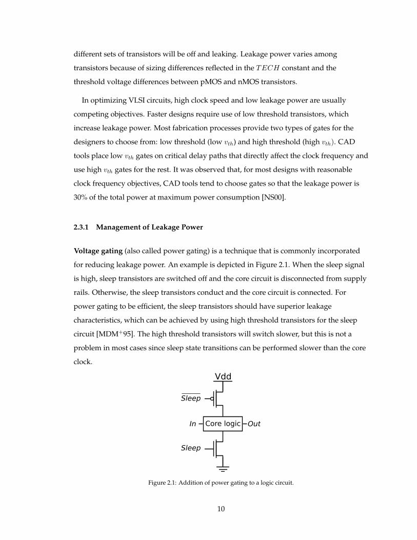
Voltage gating (also called power gating) is a technique that is commonly incorporated
for reducing leakage power. An example is depicted in Figure 2.1. When the sleep signal
is high, sleep transistors are switched off and the core circuit is disconnected from supply
rails. Otherwise, the sleep transistors conduct and the core circuit is connected. For
power gating to be efficient, the sleep transistors should have superior leakage
characteristics, which can be achieved by using high threshold transistors for the sleep
circuit [MDM+95]. The high threshold transistors will switch slower, but this is not a
problem in most cases since sleep state transitions can be performed slower than the core
clock.
Vdd
Core logic OutIn
Sleep
Sleep
Figure 2.1: Addition of power gating to a logic circuit.
10

Threshold Voltage Scaling (TVS) is another technique to to reduce leakage power.
TVS is typically applied to the the core logic transistors, unlike power gating which does
not touch the core logic. The general idea of TVS is to take advantage of the dependence
of leakage power on the threshold voltage. A higher threshold voltage reduces the
leakage power, nevertheless it also increases the gate delays hence requires the system
clock to be slowed down. The threshold voltage of a transistor can be changed during
runtime via the Adaptive Body Bias technique (ABB) [KNB+99, MFMB02] to match a
slower reference clock. ABB can be enabled during the periods that system is relatively
underloaded or clock speed is not crucial in computation.
Leakage power is also dependent on the supply voltage. Lowering the supply voltage
reduces leakage. In Section 2.6, we will review Dynamic Voltage and Frequency Scaling
(DVFS), which dynamically adjusts the voltage and frequency of the system in order to
choose a different trade-off point between clock speed and dynamic power. DVFS can
also be effective in leakage power management.
A caveat of both TVS and DVFS is the fact that they both adjust the clock frequency
dynamically, which takes time and can be limiting for fine-grained control purposes. In
Section 2.6, we discuss methods for faster clock frequency switching.
2.3.2 Estimation of of Leakage Power in Simulation
In this section, we introduce a simulation power model for leakage that complements the
model for dynamic power in Section 2.2.2.
It was previously mentioned that the leakage power of a logic gate depends on its state.
Nevertheless, as for dynamic power, bit-level estimations are unsuitable for high-level
simulators and leakage is approximated as a constant which is the average of the values
from all states. If the voltage gating technique from the Section 2.3.1 is applied, average
leakage power can be computed as:
Pleak = DUTYV × Pleak,max (2.6)
where DUTYV is the duty cycle of the unit, i.e., the fraction of time that it is not voltage
11

gated and Pleak,max is the maximum leakage power, a constant in simulation.
2.4 Power Consumption in On-Chip Memories
Most on-chip memories (caches, register files, etc.) are implemented with Static Random
Access Memory (SRAM) cells which are essentially subject to the same power
consumption and modeling equations as the CMOS logic circuits. Details of power
modeling for SRAM memories can be found in [MBJ05] and [BTM00]. In the context of
the model given in Section 2.2.2, dynamic activity of an SRAM memory (ACTmem) can be
expressed as:
ACTmem =Number of requests
Maximum number of requests(2.7)
The maximum number of requests is equal to the number of memory access ports times
the clock cycles in the measured time period.
Switching activity of caches are typically not as high as the core logic, hence dynamic
power of caches is usually not significant compared to the rest of the chip. However,
while the logic circuits can be turned off during inactive phases to save leakage power,
caches usually have to be kept alive in order to retain their data. As a result, energy due
to the leakage power of caches can add up to significant amounts over time. A solution is
threshold voltage scaling that was previously mentioned in Section 2.3.1. A cache that is
in a low power stand-by mode preserves its state, however returning to an active state in
which data can be read from it again, may add require an overhead. DVFS, which we will
discuss in Section 2.6 is another technique to reduce cache leakage with the same
overhead issue.
2.5 Power and Clock Speed Trade-offs
The delay of a logic gate (td) is a function of its supply voltage, the transistor threshold
voltage and a technology dependent constant, a (for details see Appendix A.2):
td ∝Vdd
(Vdd − vth)a(2.8)
12

In pipelined synchronous logic, the clock period is determined as the worst case
combinatorial path (a chain of stateless gates) between any pair of pipeline registers1. If
the supply and the threshold voltages are adjusted globally, this will affect the worst case
path along with the rest of the chip. Therefore, the clock period is directly proportional to
the factors that change gate delay. Clock frequency (fclock), which is the inverse of the
clock period given in Equation (2.8), can be expressed as follows:
fclock ∝(Vdd − vth)
a
Vdd≈ Vdd (2.9)
where a is set to the typical value of 2 and we assume that Vdd � vth.
Following relationship between power and clock frequency can be deduced from the
above equation and Equation (2.1) (Psw ∝ Vdd2 · f ). Assume a digital circuit that is
optimized for power, i.e. lowest supply voltage is chosen for the desired clock frequency.
If the design constraints can be relaxed in favor of a slower clock and lower Vdd, dynamic
power consumption decreases proportional to Vdd3. The Vdd is upper bound by velocity
saturation and lower bound by noise margins. Lowering Vdd, while keeping vth constant
increases noise susceptibility due to the shrinking value of Vdd − vth.
In order to reduce power, one can lower the supply and the threshold voltages together
and still be able to keep clock frequency at the same value or lower. This has been the
main driver of technology scaling for 2 decades until the practical limit of threshold
voltage scaling has been reached. The limit is basically due to the leakage power: in
Section 2.3 (Equation (2.5)), the subthreshold leakage was shown to be exponentially
proportional to the threshold voltage.
Equation (2.9) relates the clock frequency to the supply and the threshold voltages for a
fixed technology node. Between technology nodes, the die area that the same circuit
occupies shrinks because of transistor feature scaling. Lower transistor and wire area
induce proportionally lower capacitance and gate delay. As per intuition, we can say that
smaller feature sizes will reduce the electrical charge required to switch the logic states
hence the time it takes to charge/discharge with the same drive strength.
1A detailed discussion of pipelining is beyond the scope of this introduction and can be found in textbookssuch as [Rab96]
13

The channel width (W ), and length (L) are the most typical (and non-trivial)
parameters in optimizing the performance of a single gate at the transistor level. The
drive current of a MOS transistor is directly proportional to the W/L ratio and
consequently, its ability to switch the state of the next transistor in the chain. But
increasing W (assuming L is kept minimum for smaller sizes) adversely affects the
parasitic/load capacitances in the system, which, in turn, might slow down other parts of
the circuit and also increase dynamic power consumption. Moreover, W/L is one of the
factors that effect leakage power. Logic synthesis tools usually include circuit libraries
that are W/L optimized for performance so transistor sizing, in most cases, is not of
concern to system designers.
2.6 Dynamic Scaling of Voltage and Frequency
Dynamic voltage and/or frequency scaling (DVFS) is routinely incorporated in recent
processor designs as a technique for dynamically choosing a trade-off point between
clock speed and power. As we will show in Chapter 7, DVFS can be used to resolve
thermal emergencies without having to halt the computation and can also reduce the total
task energy in a energy-constrained environment.
Time
Power
P
T
Frequency = f
Vdd = V
Energy = P x T
Time
Power
P/8
2T
Frequency = f/2
Vdd = V/2
Energy = 1/4 x P x T
(a) (b)
Figure 2.2: Demonstration of dynamic energy savings with DVFS. (a) A task finishes on a serial core in timeT at 1GHz clock and 1.2V supply voltage. (b) Same task takes twice the time at half the clock frequency butconsumer 1/4 of the initial energy.
Figure 2.2 demonstrates the power reduction and energy savings made possible by
scaling the voltage and frequency of a serial core running a single task. At F GHz clock
frequency and supply voltage of V , the task finishes in time duration of T. Assume that
the frequency and voltage are lowered to half of their initial values.. At the new
14

frequency the power scales down by 1/8 and the task takes twice the time to finish. The
total energy will be reduced to 1/8× 2 = 1/4 of the initial energy. It should be noted that,
this example is excessively optimistic in assuming (a) the power only consists of dynamic
portion, and (b) the voltage can scale at the same rate as the frequency.
Scaling of voltage lowers leakage power as well, but at a rate slower than it does for
dynamic power (see Equation (2.5)). In some cases it might be more beneficial to finish
computation faster and use voltage gating introduced in Section 2.3.1 to cut off leakage
power for the rest of the time.
From a simulation point of view DVFS is characterized via two parameters: the
switching overhead and the voltage-frequency (VF) curve. Next, we will elaborate on
these factors.
Switching overhead. The overhead of DVFS depends on the implementation of
voltage and frequency switching mechanisms. As a rule of thumb, if the voltage or
frequency can be chosen from a continuous range of values, more efficient algorithms can
be implemented. However continuous voltage and frequency converters may require
significant amount of area and power, as well as the time for a transition to occur can be
in the order of µ-seconds, milliseconds or more [KGyWB08, FWR+11]. Continuous
converters are usually suitable for global control mechanisms (as in [MPB+06]) whereas
for multi and many-core processors the cost of implementing a continuous converter per
core can be prohibitively expensive. Moreover because of high time overhead,
fine-grained application of continuous DVFS may not be effective.
A fast switching mechanism (in the order of a few clock cycles overhead) allows
choosing from a limited number of frequencies and voltages. For the clock frequency,
switching is done either via choosing one of the multiple constant clock generators or
using frequency dividers on a reference clock. Voltage is usually switched between
multiple existing voltage rails. Example implementations can be found
in [LCVR03, TCM+09, Int08b, AMD04, FWR+11].
VF curve. Bulk of the savings in DVFS comes from the reduction in voltage whenever
frequency is scaled down. We used the published data on the Intel Pentium M765 and
AMD Athlon 4000+ processors [LLW10], to determine the minimum feasible voltage for a
15

Figure 2.3: VF curve for Pentium M765 and AMD Athlon 4000+ processors.
given clock frequency in GHz. The VF curve for both processors in plotted in the same
graph in Figure 2.3. The data fitted to the following formula via linear regression:
V = 0.22f + 0.86 (2.10)
where f is clock frequency in GHz and V is the voltage in Volts. We use this relation in the
implementation of DVFS for our simulator.
2.7 Technology Scaling Trends
The microprocessor industry has been following a trend that survived for the majority of
the past 45 years: in 1965 Gorden Moore observed that the number of transistors on a die
doubles with every cycle of process technology improvement (which is approximately 2
years). This trend was made possible by the scaling of transistor dimensions by 30%
every generation (die size has been growing as well but at a slower rate).
What translated “Moore’s Law” into performance scaling of serial processors was the
simultaneous scaling of power. With every generation, circuits ran 40% faster, transistor
integration doubled and power stayed the same. Below is a summary of how that was
made possible.
16

Area: 30% reduction in transistor dimensions (0.7x scaling)
Area scales by 0.7× 0.7 =∼ 0.5.
Capacitance: 30% reduction in transistor dimensions and tox.
Total capacitance scales by Cox ×W/L = 0.7× 0.7/0.7 = 0.7.
Fringing capacitance also scales 0.7x (prop. to wire lengths).
Speed: Transistor delay scales 0.7x.
Speed increases 1.4x.
Transistor power: Voltage is reduced by 30%.
Psw ∝ CLVdd2f = 0.7× 0.72 × 1.4 ≈ 0.5
Total power: Power per transistor is scaled 0.5x and count is doubled.
Ptotal0.5× 2 = 1
In addition to the 40% boost in clock speed above, doubling of the transistor count is
also reflected the performance via Pollack’s Rule. Pollack’s Rule [BC11] suggests that
doubling of transistor count will increase performance by√2 due to microarchitectural
improvements.
A few points to be noticed in the above discussion is it assumes that the transistor
power consist of only switching power (Equation (2.1), α is constant) and the reduction in
supply voltage does not reduce drive power. The former was reasonable before leakage
power became significant and the latter was maintained by reducing the threshold
voltage along with the supply voltage. As we have seen, these assumptions do not hold
in the deep sub-micron technologies.
It was the exponential relationship between threshold voltage and subthreshold
leakage power (Equation (2.5)) that broke the recipe above. Threshold voltage can no
longer be scaled without significantly increasing the leakage power. Thus, keeping the
drive power (and the speed) constant requires supply voltage to stay constant as well. If
the supply voltage is not scaled, clock frequency cannot be boosted without increasing
dynamic power. Note that Moore’s Law is still being followed today (even though it has
its own challenges) but performance growth can no longer rely on clock frequency and
inefficient microarchitectural techniques. Instead, silicon resources are used towards
increasing on-chip parallelism. Parallel machines can provide performance in the form of
multi-tasking, however increasing the performance of a single task no longer comes at no
17

cost to the programmers since the programs have to be parallelized.
2.8 Thermal Modeling and Design
Temperature rises on a die as a result of heat generation, which is due to the power
dissipated by the circuits on it. The relationship between power and temperature is often
modeled analogously to the voltage and current relationship in a resistive/capacitive
(RC) circuit [SSH+03]. Figure 2.4(a) shows such an equivalent RC circuit. i is the input
current and V is the output voltage. The counterparts of i and V for thermal modeling are
power and temperature, respectively. Rdie and Rhs are the die and heat sink thermal
resistances (K/W is the unit of thermal resistance). Temperature responds gradually to a
sudden change in power, as voltage does with current in RC circuits. The gradual
response of temperature to power filters out short spikes in power, which is called
temporal filtering.
The example in Figure 2.4(c) demonstrates the case where the power is a rectangle
function (two step functions). The initial phase before temperature stabilizes is named the
transient-response and the stable value that comes after the transient is the steady-state
response. In the steady-state, the circuit is equivalent to a pure resistive network since
capacitances act as open circuits when they are charged. The resistive equivalent of
Figure 2.4(a) is given in Figure 2.4(b). As a result, steady-state temperature is
proportional to the power (V = i ·R). In typical microchips, the transient response may
last in the order of milliseconds.
The discussion above focused on the time-response of the temperature to a point heat
source. It is also important to analyze the spatial distribution of temperature on the
silicon die where the circuits are printed. A common microchip is a three dimensional
structure that consists of a silicon die, a heat spreader and a heat sink. Temperature
estimation tools such as the one in [SSH+03] model this structure as a distributed RC
network, solution methods for which are well known. Figure 2.5 is an example of a chip
with the cooling system and its RC equivalent.
In this thesis, we only consider cooling systems that are mounted on the surface of the
chip packaging, heatsinks, which are dominant in commercial personal computers. The
18

i
V
Vamb
Rdie
Rhs
i
V
Vamb
Rdie
Rhs
(a) (b)
(c)
Figure 2.4: Modeling of temperature and heat analogous to RC circuits. (a) Equivalent RC circuit. (b) Equiva-lent RC circuit in steady-state. (c) Time response of the circuit to a rectangle function (which is the combinationof a rising and a falling step function).
efficiency of a cooling system is measured in the amount of power density that it can
remove while keeping the chip below a feasible temperature. The most affordable of
surface mounted systems is air cooling and it is estimated to last in the market until the
power densities reach approximately 1.5W/mm2 [Nak06]. Currently, 0.5W/mm2 is
typical for high-end processors (see next section). An equivalent measure of the efficiency
for a heatsink is the convection resistance (Rc) between the heatsink and the environment.
We will give typical values for Rc in Section 2.9.
Temperature constraints can be very different than power constraints especially if
power is distributed unevenly on the die. Temperature rises more at areas that have
higher power density. The hottest areas of a chip are termed thermal hot-spots and the
cooling system should be designed so that it is able to remove the heat from hot-spots.
Even though the hot-spots dictate the cost of cooling mechanism, they might cover only a
small portion of the chip area, which is the reason for the difference between power and
thermal constraints. For example, assume that a 200mm2 chip has an average power
density of 0.1W/mm2 and a hot-spot that dissipates 0.5W/mm2 (numbers are chosen for
illustrative purposes). The total power of the chip is 20mm2 however the cooling
19

Heatsink
Heat spreader
Heatsink
Package, I/O, PCB,...
Silicon Die
Heatsink
Heat spreader
Silicon Die
Rconv
Tamb
(a) (b)
Figure 2.5: (a) Side view of a typical chip with packaging and heat sink. (b) Simplified RC model for the chip.
mechanism should be chosen for 0.5W/mm2 and it capable of removing 100W . This
observation motivated a magnitude of research in managing chip temperature, which we
will review in Chapter 7.
Hot-spots can be severe especially in superscalar architectures, where the power
dissipated by different architectural blocks can vary by large amounts. An example is
demonstrated for a IBM PowerPC 970 processor (based on the Power 4 system [BTR02])
in Figure 2.6 [HWL+07]. The PowerPC 970 core consists of a vector engine, two FXUs
(fixed point integer unit), and ISU (instruction sequencing unit), two FPUs (floating-point
unit), two LSUs (load-store unit), an IFU (instruction fetch unit) and an IDU (instruction
decode unit). The thermal image was taken during the execution of a high power
workload and clearly shows that there is a drastic temperature difference between the
core and the caches. This behavior is quite common in processors where caches and logic
intensive cores are isolated.
In many-cores with simpler computing cores and distributed caches, the cores can be
scattered across the chip, alternating with cache modules. Due to the spatial filtering of
temperature [HSS+08], the issue of thermal hot-spots may not be as critical for such
floorplans. Basically, when high power small heat sources (i.e., cores) are padded with
low power spaces in between (i.e., caches) the temperature spreads evenly. The peak
temperature will not be as high as if the cores were to be lumped together. The floorplan
that we propose for XMT in Section 7.3 is motivated by this observation.
20

Figure 2.6: Thermal image of a single core of IBM PowerPC 970 processor. The thermal figure and floorplanoverlay are taken from [HWL+07, HWL+07], respectively.
2.9 Power and Thermal Constraints in Recent Processors
Processor cooling systems are usually designed for the “typical worst-case” power
consumption. It is very rare that all, or even most, of the sub-systems of a processor are at
their maximum activity simultaneously. A 1W increase in the specifications of the cooling
system costs in the order of $1-3 or more per chip when average power exceeds
40W [Bor99]. Therefore, it would not be cost efficient to design the cooling system for the
absolute worst-case. The highest feasible power for the processor is defined as the
thermal design power (TDP). Most low to mid-grade computer systems implement an
emergency halt mechanism to deal with the unlikely event of exceeding TDP. More
advance processors continuously monitor and control temperature.
Table 2.1 is the survey of a representative set of commercial processors as of 2011. The
GPUs (GTX280 and Radeon HD 6970) are many-core processors with lightweight cores
and the remainder are more traditional multi-cores. The power densities range from
0.44W/mm2 to 0.64W/mm2. The maximum temperature listed for all processors are close
to 100C.
The value of the heatsink convection resistance is a controlled parameter in our
simulations for reflecting the effect of low, mid and high grade air cooling mechanisms.
These values are 0.5K/W , 0.1K/W , and 0.05K/W , which are representatives of
commercial products.
21

Processor TDP Max. Clock Freq. Die Area CoresCore i7-2600 [Inta] 95W 1.35GHz 216mm2 4
Power7 750 [BPV10] ∼350W 3.55GHz 567mm2 8Phenom II X4 840 [AMD10a] 95W 3.2GHz 169mm2 4
GTX 580 [NVIb] 244W 1.5GHz 520mm2 512Radeon HD 6970 [AMD10b] 250W 880MHz 389mm2 1536
Table 2.1: A survey of thermal design powers.
2.10 Tools for Area, Power and Temperature Estimation
Academia and industry have developed a number of tools to aid researchers who
develop simulators for early-stage exploration of architectures. We list the ones that stand
out as they are highly cited in research papers. Architecture simulators, including our
own XMTSim described in Chapter 4, can interface with these tools to generate runtime
power and temperature estimates.
Cacti [WJ96, MBJ05] and McPAT [LAS+09] estimate the latency, area and the power of
processors under user defined constraints. More specifically, Cacti models memory
structures, mainly caches, and McPAT explores full multi-core systems. McPAT internally
uses Cacti for caches and projects the rest of the chip from existing commercial
processors. McPAT cannot be configured to estimate the power of an XMT chip directly,
however it can still be used to generate parameters for microarchitectural components
simulated in XMTSim, including execution units and register files. Section 6.1 is an
example of how McPAT and Cacti outputs can be used in XMTSim.
HotSpot [HSS+04, HSR+07, SSH+03] is an accurate and fast thermal model that can be
included in an architecture simulator to generate the input for thermal management
algorithms or other stages that are temperature dependent, for example leakage power
estimation. It views the chip area as a finite number of blocks each of which is a 2
dimensional heat source. In order to solve the temperatures based on the power values, it
borrows from the concepts that describe the voltage and current relationships in
distributed RC (resistive/capacitive) circuits. HotSpot has inherent shortcomings because
of the hardness of estimating or even directly measuring the temperature in complex
systems, and it can only model air cooling solutions. However, it still is the most
frequently used publicly-available temperature model for academic high-level simulators.
22

HotLeakage [ZPS+03] is an architectural model for subthreshold and gate leakage in
MOS circuits. As its input, it takes the die temperature, supply voltage, threshold voltage
and other process technology dependent parameters and estimates the leakage variation
based on these inputs. In Section 2.3, we have briefly reviewed the leakage power
equation which was derived from the HotLeakage model.
23

Chapter 3
The Explicit Multi-Threading (XMT) Platform
The primary goal of the eXplicit Multi-Threading (XMT) general-purpose computer
platform [NNTV01, VDBN98] has been improving single-task performance through
parallelism. XMT was designed from the ground up to capitalize on the huge on-chip
resources becoming available in order to support the formidable body of knowledge,
known as Parallel Random Access Model (PRAM) algorithmics, and the latent, though
not widespread, familiarity with it. Driven by the repeated programming difficulties of
parallel machines, ease-of-programming was a leading design objective of XMT. The
XMT architecture has been prototyped on a field-programmable gate array (FPGA) as a
part of the University of Maryland PRAM-On-Chip project [WV08a, WV07, WV08b]. The
FPGA prototype is a 64-core, 75MHz computer. In addition to the FPGA, the main
medium for running XMT programs is a highly configurable cycle-accurate simulator,
which is one of the contributions of this dissertation.
The PRAM model of computation [JáJ92, KR90, EG88, Vis07] was developed during the
1980s and early 1990s to address the question of how to program parallel algorithms and
was proven to be very successful on an abstract level. PRAM provides an intuitive
abstraction for developing parallel algorithms, which led to an extremely rich algorithmic
theory second in magnitude only to its serial counterpart known as the “von-Neumann”
architecture. Motivated by its success, a number of projects attempted to carry PRAM to
practice via multi-chip parallelism. These projects include
NYU-Ultracomputer [GGK+82] and the Tera/Cray MTA [ACC+90] in the 1980s and the
SB-PRAM [BBF+97, KKT01, PBB+02] in the 1990s. However the bottlenecks caused by the
speed, latency and bandwidth of communication across chip boundaries made this goal
difficult to accomplish (as noted in [CKP+93, CGS97]). It was not until 2000s that
technological advances allowed fitting multiple computation cores on a chip, relieving
the communication bottlenecks.
24

Figure 3.1: Overview of the XMT architecture.
The first three sections of this chapter gives an overview of the XMT architecture, its
programming and performance advantages. Section 3.5 discusses various aspects of XMT
from a power efficiency and management perspective.
3.1 The XMT Architecture
The XMT architecture, depicted in Figure 3.1, consists of an array of lightweight cores,
Thread Control Units (TCUs), and a serial core with its own cache (Master TCU). TCUs
are arranged in clusters which are connected to the shared cache layer by a
high-throughput Mesh-of-Trees interconnection network (MoT-ICN) [BQV09]. Within a
cluster, a compiler-managed Read-Only Cache is used to store constant values across all
threads. TCUs incorporate dedicated lightweight ALUs, but the more expensive
Multiply/Divide (MDU) and Floating Point Units (FPU) are shared by all TCUs in a
cluster.
The memory hierarchy of XMT is explained in detail in Section 3.1.1. The remaining
on-chip components are an instruction and data broadcast mechanism, a global register
file and a prefix-sum unit. Prefix-sum (PS) is a powerful primitive similar in function to
the NYU Ultracomputer Fetch-and-Add [GGK+82]; it provides constant, low overhead
inter-thread coordination, a key requirement for implementing efficient intra-task
parallelism (see Section 3.2.3).
25

045111231
Address inside module Module ID
Figure 3.2: Bit fields in an XMT memory address.
3.1.1 Memory Organization
The XMT memory hierarchy does not include private writable caches (except for the
Master TCU). The shared cache is partitioned into mutually exclusive modules, sharing
several off-chip DRAM memory channels. A single monolithic cache with many
read/write ports is not an option since the cache speed is inversely proportional to the
cache size and number of ports. Cache coherence is not an issue for XMT as the cache
modules are mutually exclusive in the addresses that they can accommodate. Caches can
handle new requests while buffering previous misses in order to achieve better memory
access latency.
XMT is a Uniform Memory Access (UMA) architecture: all TCUs are conceptually at at
the same distance from all cache modules, connected to the caches through a symmetrical
interconnection network. TCUs also feature prefetch buffers, which are utilized via a
compiler optimization to hide memory latencies.
Contiguous memory addresses are distributed among cache modules uniformly to
avoid memory hotspots. They are distributed to shared cache modules at the granularity
of cache lines: addresses from consecutive cache lines reside in different cache modules.
The purpose of this scheme is to increase cache parallelism and reduce conflicts on cache
modules and DRAM ports. Figure 3.2 shows the bit fields in a 32-b memory address for
an XMT configuration with 128 cache modules and 32-bit cache lines. The least significant
5 bits are reserved for the cache-line address. The next 7 bits are reserved for addressing
cache modules and the remainder is used for the address in a cache module.
3.1.2 The Mesh-of-Trees Interconnect (MoT-ICN)
The interconnection network of XMT complements the shared cache organization in
supporting memory traffic requirements of XMT programs. The MoT-ICN is specifically
designed to support irregular memory traffic and as such contributes to the
ease-of-programming and performance of XMT considerably. It is guaranteed that unless
26

N x N connection
Fan-out layer
Fan-in layer
Figure 3.3: The concept of Mesh-of-Trees demonstrated on a 4-in, 4-out configuration.
(a) (b)
Figure 3.4: Building blocks of MoT-ICN: (a) fan-out tree, (b) fan-in tree.
the memory access traffic is extremely unbalanced, packets between different sources and
destinations will not interfere. Therefore, the per-cycle throughput provided by the MoT
network is very close to its peak throughput and it displays low contention under
scattered and non-uniform requests.
Figure 3.3 is a high level overview of the 4-to-4 MoT topology. The building blocks of
the MoT-ICN, binary fan-out and fan-in trees, are depicted in Figures 3.4(a). The network
consists of a layer of fan-out trees at its inputs and a layer of fan-in trees at its the outputs.
For an n-to-n network, each fan-out tree is a 1-to-n router and each fan-in tree is a n-to-1
arbiter. The fan-in and fan-out trees are connected so that there is a path from each input
to each output. There is a unique path between each source and each destination. This
simplifies the operation of the switching circuits and allows faster implementation which
27
translates into improvement in throughput when pipelining a path. More information
about the implementation of MoT-ICN can be found in [Bal08].
3.2 Programming of XMT
3.2.1 The PRAM Model
A parallel random access machine employs a collection of synchronous processors.
Processors are assumed to access a shared global memory in unit time. In addition, every
processor contains a local memory (i.e. registers) for calculations within the thread it
executes. Among various strategies to resolve access conflicts to the shared memory,
arbitrary CRCW (concurrent read, concurrent write) and QRQW (queue read, queue
write) rules are relevant to our discussion since the XMT processor follows a model that is
the hybrid of the two. In the arbitrary CRCW, concurrent write requests by multiple
processors result in the success of an arbitrary one. Concurrent reads are assumed to be
allowed at no expense. The prefix-sum instruction of XMT, explained in Section 3.2.3,
provides CRCW-like access to memory. On the other hand, the QRQW rule does not
allow concurrent reads or writes, and instead requests that arrive at the same time are
queued in an arbitrary order. All memory accesses in XMT other than prefix-sum are
QRQW-like. These two strategies have the same consequence, that is, only one succeeds
among all requests that arrive at the same time. However, the execution mechanism and
latencies are different (i.e., concurrent access versus queuing).
The next example shows a short snippet code that adds one to each element in array B
and writes the result in array A. Arrays A and B are assumed to be of size n. According to
the PRAM model, this operation executes in constant time, given that each parallel thread
i is carried by a separate processor.
for 1≤i≤n do in parallel
A(i) := B(i) + 1
XMT aims to give performance that is proportional to the theoretical performance of
PRAM algorithms. The programmer’s workflow of XMT provides means to start from a
28

PRAM algorithm and produce a performance optimized program [Vis11], analogous to
the traditional programming of serial programs. XMT does not try to implement PRAM
exactly. In particular, certain assumptions of PRAM are not realistic from an
implementation point of view. These assumptions are:
• Constant access time to the shared memory. While this assumption is unrealistic
for any computer system, XMT attempts to minimize access time by shared caches
specifically designed for serving multiple misses simultaneously. True constant
access time on a limited number of global registers is implemented via prefix-sum
operation (see Section 3.2.3).
• Unlimited number of virtual processors. XMT programs are independent of the
number of processors in the system. Hardware automatically schedules the threads
to run on a limited number of physical TCUs.
• Lockstep Synchronization. The lockstep synchronization of each parallel step in
PRAM is not infeasible for large systems from a performance and power point of
view. XMT programming model relaxes this specification of PRAM.
3.2.2 XMTC – Enhanced C Programming for XMT
The parallel programs of XMT are written in XMTC, a modest extension of the
C-language with alternating serial and parallel execution modes. The spawn statement
introduces parallelism in XMTC. It is a type of parallel “loop” whose “iterations” can be
executed in parallel. It takes two arguments low, and high, and a block of code, the
spawn block. The block is concurrently executed on (high-low+1) virtual threads. The ID of
each virtual thread can be accessed using the dollar sign ($) and takes integer values
within the range low ≤ $ ≤ high. Variables declared in the spawn block are private to
each virtual thread. All virtual threads must complete before serial execution resumes
after the spawn block. In other words, a spawn statement introduces an implicit
synchronization point. The number of virtual threads created by a spawn statement is
independent from the number of TCUs in the XMT system. XMT allows concurrent
instantiation of as many threads as the number of available processors. Threads are
efficiently started and distributed thanks to the use of prefix-sum for fast dynamic
29

allocation of work, and a dedicated instruction broadcast bus. The high-bandwidth
interconnection network and the low-overhead creation of many threads facilitate
effective support of fine-grained parallelism. An algorithm designed following the XMT
workflow [Vis11] permits each virtual thread to progress at its own speed, without ever
having to busy-wait for other virtual threads.
3.2.3 The Prefix-Sum Operation
In XMTC programming PS operations are typically used for load balancing and
inter-thread synchronization. It is also implicitly used in thread scheduling, which is
explained in Section 3.3. PS is an atomic operation that increments the value in a global
base register G by the value in a local thread register R and overwrites the value in R with
the previous value of G.
Gn+1 ← Gn +Rn
Rn+1 ← Gn
Even though this operation is similar to Fetch-and-Add in [GGK+82], its novelty lies in
the fact that a PS operation completes execution in constant time, independent of the
number of parallel threads concurrently trying to write to that location. The PS hardware
only ensures atomicity but the commit order is arbitrary for concurrent requests. For
example, a group of concurrent prefix-sum operations from different TCUs with local
registers 0, 1 and 2 to a global base register G will result in
Gn+1 ← Gn +Rn,0 +Rn,1 +Rn,2
Rn+1,0 ← Gn
Rn+1,1 ← Gn +Rn,0
Rn+1,2 ← Gn +Rn,0 +Rn,1
30

Any other order is also possible, as in
Gn+1 ← Gn +Rn,0 +Rn,1 +Rn,2
Rn+1,2 ← Gn
Rn+1,0 ← Gn +Rn,2
Rn+1,1 ← Gn +Rn,2 +Rn,0
Due to the hardware implementation challenges, the incremental values are limited to
0 and 1. Also, the base register can only be a global register. XMT also provides an
unrestricted version of PS, prefix-sum to memory (PSM) for which the base can be any
memory address and the increment values are not limited. However, PSM operation does
not give the same performance as PS since PSM is essentially an atomic memory
operation that is serialized with other memory references at the shared caches.
3.2.4 Example Program
An example of a simple XMTC program, Array Compaction, is provided in Figure 3.5(a).
In the program, the non-zero elements of array A are copied into an array B, with the
order not necessarily preserved. The spawn instruction creates N virtual threads; $ refers
to the unique identifier of each thread. The prefix-sum statement ps(inc,base) is
executed as an atomic operation. The base variable is incremented by inc and the the
original value of base is assigned to the inc variable. The parallel code section ends
with an implicit join instruction. Figure 3.5(b) illustrates the flow of an XMT program
with two parallel spawn sections.
3.2.5 Independence-of-Order and No-Busy-Wait
XMT programs usually do not include coordination code other than prefix-sums and
threads can only communicate through shared memory and global registers via the
31

int A[N],B[N],base=0;spawn(0,N-1) {int inc=1;if (A[$]!=0) {ps(inc,base);B[inc]=A[$];
}}
spawn
join
spawn
join$
(a) (b)
Figure 3.5: (a) XMTC program example: Array Compaction. (b) Execution of a sequence of spawn and joincommands.
CRCW/QRQW memory model. Due to these properties threads can be abstracted as
virtual No-Busy-Wait (NBW) finite state machines, where each TCU progresses at an
independent rate without blocking another. The No-Busy-Wait paradigm yields much
better performance results than tightly coupled parallel architectures, such as Vector or
VLIW processors. In addition to NBW, XMTC programs also exhibit Independence of Order
Semantics (IOS): the correctness of an XMTC program should be independent of the
progression rate and completion order of individual threads.
3.2.6 Ease-of-Programming
Ease-of-programming (EoP) is a goal that has long eluded the field of parallel
programming. The emergence of on-chip parallel computers in the general-purpose
domain exacerbates the problem now that parallel architectures are targeting a large
programmer base and a wider variety of applications. Among these, programs with
irregular memory access and parallelism patterns are frequent in the general-purpose
domain and they are considered among the hardest problems in parallel computing
today. These programs defy optimizations, such as programming for locality, that are
common in typical many-cores, and require significant programming effort to obtain
minor performance improvements. More information and examples on irregular versus
regular programs will be given in Section 5.3.
EoP is one of the main objectives of XMT: considerable amount of evidence was
developed on ease of teaching [TVTE10,VTEC09] and improved development time with XMT
32

Serial Code
TIDlow ← N + IDfirst
TIDhigh ← IDlast
Broadcast IDfirst
Spawn
TIDlow - TIDhigh > N
Serial Code
Yes
$ = IDfirst + TCUID
$ ≤ TIDhigh
Parallel Code
$ = PS(TIDlow,1)
Yes
Master TCU
Parallel TCUs
Star
t al
l TCUs
No
No
Figure 3.6: Flowchart for starting and distributing threads.
relative to alternative parallel approaches including MPI [HBVG08], OpenMP [PV11] and
CUDA (experiences in [CKTV10]). XMT provides a programmer’s workflow for deriving
efficient programs from PRAM algorithms, and reasoning about their execution
time [VCL07] and correctness. The architecture of XMT was specifically built to handle
irregular parallel programs efficiently, which is one of the reasons for its success in EoP.
Complex optimizations are often not needed in order to obtain performance advantages
over serial for these programs.
In a joint teaching experiment between the University of Illinois and the University of
Maryland comparing OpenMP and XMTC programming [PV11], none of the 42 students
achieved speedups using OpenMP programming on the simple irregular problem of
breadth-first search (Bfs) using an 8-processor SMP, but all reached speedups of 8x to 25x
on XMT. Moreover, the PRAM/XMT part of the joint course was able to convey
algorithms for more advanced problems than the other parts.
33

3.3 Thread Scheduling in XMT
XMT features a novel lightweight thread scheduling/distribution mechanism. Figure 3.6
provides the algorithm for starting a parallel section, distributing the threads among the
TCUs and returning control to the Master TCU upon completion. The detail level of the
algorithm roughly matches the assembly language, meaning that each stage in the
algorithm corresponds to an assembly instruction. Most important of these mechanisms
is the prefix-sum (PS), on which thread scheduling is based.
The algorithm in Figure 3.6 is for one spawn block with thread ID (TID) numbers from
IDfirst to IDlast (recall that XMT threads are labeled with contiguous ID numbers).
Master TCU first initializes two special global registers: TIDlow and TIDhigh. These two
registers, contain the range of ID numbers of the threads that have not been picked up by
TCUs. Spawn broadcasts parallel instructions and sends a start signal to all TCUs present
in the system. Master TCU broadcasts the value of IDfirst by embedding it into the
parallel instructions. TCUs start executing parallel code with assigned thread IDs ($) from
TCUID to TCUID +N − 1, where N is the number of TCUs. TCUID is the hardcoded
identifier of a TCU, a number between 0 and N − 1. TCUs with invalid thread IDs (i.e.,
$ > TIDhigh) will wait for new work to become available (it is possible that an active
thread modifies TIDhigh, therefore dynamically changes the total number of threads to be
executed). $ = PS(TIDlow, 1) serves the double purpose of returning a new thread ID for
a TCU that just finished a thread and also updating the range of threads that are not yet
picked up. When all TCUs are idle, which implies TIDlow − TIDhigh = N + 1, the
parallel section ends and master TCU proceeds with serial execution.
Figure 3.7 is an example of how seven threads, with IDs from 0 to 6, are started and
scheduled on a 4-TCU XMT configuration. Below are the explanations that correspond to
each step in the figure.
a) TCUs initially start with thread IDs equal to their TCUIDs therefore the threads that
are not yet picked up are 4 to 6.
b) In this example, TCU 2 finishes its thread first so it picks up the next thread ID, 4.
c) Then TCUs 1 and 3 finish simultaneously and pick up threads with IDs 5 and 6 in
arbitrary order.
34

TCU0
TID0=7
Idle
TCU2
Finished
TCU0
TID0=0
Executing...
TCU1
TID1=1
Executing...
TCU2
TID2=2
Executing...
TCU3
TID3=3
Executing...
TIDlow = 4
TIDhigh = 6
TCU0
TID0=0
Executing...
TCU1
TID1=1
Executing...
TCU2
Finished
TCU3
TID3=3
Executing...
TIDlow = 4
TIDhigh = 6
TID2=PS(TIDlow,1)
TCU0
TID0=0
Executing...
TIDlow = 5
TIDhigh = 6 TID3=PS(TIDlow,1)
TCU2
TID2=4
Executing...
TID1=PS(TIDlow,1)
TCU3
Finished
TCU1
Finished
TCU1
TID0=6
Executing...
TIDlow = 7
TIDhigh = 6
TCU2
TID2=4
Executing...
TCU0
Finished
TCU2
TID2=5
Executing...
TID0=PS(TIDlow,1)
TCU0
TID0=7
Idle
TIDlow = 8
TIDhigh = 6TID3=PS(TIDlow,1)
TID1=PS(TIDlow,1)
TCU3
Finished
TCU1
Finished
TCU1
TID0=9
Idle
TIDlow = 11
TIDhigh = 6
TCU2
TID2=8
Idle
TCU2
TID2=10
Idle
TID2=PS(TIDlow,1)
(a)
(b)
(e)
(b)
(d)
(f)
Figure 3.7: Execution of a parallel section with 7 threads on a 4-TCU XMT system. N is the number of TCUsin the system. Refer to text for a detailed explanation of the example.
d) TCU 0 finishes thread 0 and picks up thread ID 7, which is invalid at the moment.
TCU 0 starts waiting, in case one of the currently executing threads creates thread 7
by incrementing TIDhigh.
e) The remainder of the TCUs finish their threads and pick up invalid thread IDs as
well.
f ) At the final state, all TCUs are idling and TIDlow − TIDhigh = 5. This is the
condition to end a parallel section and control returns to the Master TCU.
35

3.4 Performance Advantages
It was shown that a cycle-accurate 64-core FPGA hardware XMT
prototype [WV07, WV08a] outperforms an Intel Core 2 Duo processor [CSWV09], despite
the fact the Intel processor uses more silicon resources. A comparison of FFT (the Fast
Fourier Transform) on XMT and on multi-cores showed that XMT can both get better
speedups and achieve them with less application parallelism [STBV09]. In Section 5.4, we
will present a study, in which we simulate a 1024-core XMT chip, that is silicon-area and
power equivalent to an NVIDIA GTX280 many-core GPU. We show that, in addition to
being easier to program than the GPU, XMT also has the potential of coming ahead in
performance.
Many doubt the practical relevance of PRAM algorithms, and past work provided very
limited evidence to alleviate these doubts; [CB05] reported speedups of up to 4x on
biconnectivity using a 12-processor Sun machine and [HH10] up to 2.5x on maximum
flow using a hybrid CPU-GPU implementation when compared to best serial
implementations. New results, however, show that parallel graph algorithms derived
from the PRAM theory can provide significantly better speedups than alternative
algorithms. These results include potential speedups of 5.4x to 73x on breadth-first search
(Bfs) and 2.2x to 4x on graph connectivity when compared with optimized GPU
implementations. Also, with respect to best serial implementations on modern CPU
architectures, we observed potential speedups of 9x to 33x on biconnectivity [Edw11],
and up to 108x on maximum flow [CV11].
3.5 Power Efficiency of XMT and Design for Power Management
Several architectural decisions in XMT, such as the lightweight cores, thread
synchronization (via the join mechanism) and thread scheduling, as well as the lack of
private local caches (hence, of power-hungry cache coherence) are geared towards energy
efficient computation. It is the synergy of the cores that accelerate a parallel program over
a serial counterpart rather than the performance of a single thread. In the remainder of
this section, we overview several aspects of XMT from a power efficiency and
36

management point of view.
3.5.1 Suitability of the Programming Model
In Chapter 7, we will see that efficient dynamic thermal and power management of a
parallel processor may require the ability to independently alter the execution of its
components (for example, cores). In XMT, execution of the TCUs can be individually
modified without creating a global bottleneck. This is facilitated by its programming
model, which we explain next.
The No-Busy-Wait paradigm and Independence of Order Semantics of XMT naturally
fit the Globally Asynchronous, Locally Synchronous (GALS) style design [MVF00], in which
each one of the clusters operate in a dedicated clock domain. Moreover, the ICN and the
shared caches can operate in separate clock domains as there is no practical reason for
any of these subsystems to be tightly synchronized. Clusters, caches and the ICN can
easily be designed to interface with each other via FIFOs. As explained above, the relaxed
synchrony does not hurt the XMT programming model. In fact, XMT was built on the
idea of relaxing the strict synchrony of PRAM model. In Chapter 7 we will evaluate
various clocking schemes for XMT inspired by the ideas above. The programming model
of XMT is also suitable for a power-efficient asynchronous ICN, as demonstrated recently
in [HNCV10].
As we will discuss in the next section, XMT threads can be easily dispatched to the
different parts of the die by temporarily preventing the TCUs from requesting threads
from the pool, should it be necessary for avoiding thermal emergencies. It is important to
note that this is possible because a) XMTC programs do not rely on the number of TCUs
for correct and efficient implementation, b) threads in XMTC programs are typically
shorter compared to thermal time constants, and c) there is no complex work distribution
algorithm that interferes with the routing of threads.
3.5.2 Re-designing Thread Scheduling for Power
The implementation of thread scheduling in the FPGA prototype, reviewed in Section 3.3,
is not optimized for power efficiency and power management was not one of its design
37

$ = IDfirst + TCUID
$ ≤ TIDhigh
Parallel Code
$ = PS(TIDlow,1)
Yes
Parallel TCUs
No
Global Thread
Monitor
TCUID, $
Stall
$ ≤ TIDhigh
Figure 3.8: Sleep-wake mechanism for thread ID check in TCUs.
specifications. In this section, we list two potential improvements: sleep-wake for
reducing the power of idling TCUs and thread gating for controlling the assignment of
threads to TCUs. Both of these mechanisms are incorporated into our cycle-accurate
simulator. The effect of sleep-wake is included by default in the results presented in
Chapters 6 and 7. Thread gating is applied to equally distribute the power across the
cores whenever the number of active threads is less than the number of TCUs.
Sleep-Wake vs. Polling for Thread ID Check
The first change that we propose is an energy efficient implementation of the TCU
thread ID check step ($ ≤ TIDhigh) in Figure 3.6. In the current implementation, the
corresponding assembly instruction is a branch that continuously polls on the condition
until it is satisfied. This polling mechanism, in addition to wasting dynamic power, also
prevents a potential power management algorithm from putting the TCU to a low-power
mode to save static power.
Figure 3.8 (based on Figure 3.6) illustrates the proposed sleep-wake mechanism. When a
TCU reaches the condition and fails at the first attempt, it sends its unique ID (TCUID in
Figure 3.6) along with the new thread ID ($) to a global controller and stalls. The global
controller monitors TIDhigh for changes and “wakes up” the TCU if its stored thread ID
becomes active.
Implementation of a sleep-wake mechanism for the parallel TCUs is especially
important since the cost of polling is multiplied by the number of TCUs. Another step in
38

$ = IDfirst + TCUID
$ ≤ TIDhigh
Parallel Code
$ = PS(TIDlow,1)
Yes
Parallel TCUs
Continue?
Yes
No
Continue
Set condition
No
Global Thread
Monitor
TCUID, $
Stall
$ ≤ TIDhigh
Figure 3.9: Addition of thread gating to thread scheduling of XMT. Original mechanism was given in Fig-ure 3.8.
Figure 3.6 where polling appears is the TIDlow − TIDhigh > N condition of the Master
TCU. However, optimization of this step is not as critical since it is only executed by
Master TCU.
Thread Gating
A straightforward addition to the thread scheduling mechanism is the ability to
modulate the distribution of threads to the clusters dynamically during the runtime in
order to reduce the power at certain areas of the chip. We will call this feature thread
gating.
The change proposed for incorporating thread gating to the mechanism in Figure 3.8 is
shown in Figure 3.9. The general idea is to reduce the number of active TCUs and limit
the execution to a subset of all TCUs in the system. Given a TCU selected for thread
gating, the algorithm will let the TCU run to the completion of its current thread and
prevent it from picking up a new one. A thread gated TCU can be put in a low power
stand-by mode and later can be awaken to proceed. This system is deadlock-free as the
TCU is stopped right before it picks up a new thread so none of the virtual threads
created so far or that can yet be created dynamically resides in the gated TCU.
It should be noted that thread gating relies on the fact that in fine-grained parallelism,
39

Active
IdleMWait
Response
Mem-op
T-Gate?
No
Yes
T-Gated
End of thread
$ ≤ TIDhigh
Release
Start
Figure 3.10: The state diagram for the activity state of TCUs.
threads are usually short and the control algorithm can afford to wait until the executing
threads are finished before the selected TCUs can be gated. This assumption holds in the
majority of the cases, especially for thermal management. The time scale of temperature
changes, as we have discussed in Section 2.8, is usually orders of magnitude higher
compared to typical XMTC threads. Nevertheless, if thread gating is used for a critical
task such as prevention of thermal emergencies, a fall back should be implemented. In
most processors the fall back is a system-wide halt of the clock.
3.5.3 Low Power States for Clusters
We envision that an industry grade XMT system will be capable of stopping the clock of
the TCUs that are waiting on memory operations or not executing a thread. This can
provide substantial savings in dynamic power. If none of the TCUs in a cluster is
executing threads, the cluster can be voltage gated for saving leakage power. In this
section, we discuss how these optimizations can be implemented. These optimizations
are incorporated into the simulations of Chapter 7.
We assume that a TCU can be in one of the following four states: (a) active – executing
an XMTC thread and not waiting on a memory operation, (b) mwait – waiting on a
memory operation, (c) idle – blocked at the thread ID check (see Figure 3.6), and (d)
t-gated1 – TCU is gated by global control as explained in the previous subsection. A
t-gated TCU does not contain any state. In the idle state, values of the program counter
(PC) and the thread ID ($), and in the mwait state, the values in all registers and the PC
1 We use t-gated to prevent confusion with clock or voltage gating. It stands for thread-gated.
40

should be kept alive. Figure 3.10 summarizes the TCUs activity states.
Any TCU that is not in the active state can individually be clock gated. Non-active
states (especially mwait) can happen at short time intervals and clock gating can be
applied successfully since it typically does not cost additional clock cycles. The power
model that we later introduce in Section 4.5 assumes that clock gating is implemented for
TCUs.
Voltage gating is usually implemented at coarser grain and causes the information in
the registers to be lost. For XMT, cluster granularity is suitable. For a cluster to be voltage
gated, all TCUs in it should be in one of the t-gated or idle states. The mwait state, which
requires the registers and the PC to be alive, is not considered for this mechanism. Even
though, thread ID should not be lost in the idle state, it is already saved to the thread
monitor (see Figure 3.9).
A voltage gated cluster can also turn off other components in it, such as the functional
units and the ICN access port. If the instruction cache is also turned-off, the instructions
in it will be lost and upon returning to active state, it will have to be loaded again costing
in performance.
3.5.4 Power Management of the Synchronous MoT-ICN
We will elaborate on challenges and ideas in managing the dynamic and leakage power
of ICN. Note that, efficient management of dynamic and leakage power in
interconnection networks is an open research question not only for XMT, but for most
architectures [MOP+09]. For this reason, the future plan for XMT is a power efficient
asynchronous ICN [HNCV10].
Dynamic Power. The MoT-ICN trees (depicted in Figure 3.4) consist of lightweight
nodes that are distributed along the routing paths. Due to simplicity of the nodes, trees
might not benefit from fine-grained clock gating (see Section 2.2.1). On the other hand,
clock gating at a coarser grain, for example tree level, might introduce other difficulties.
Turning the clock of a whole tree on and off might require more than one clock cycle
because the trees, on average, are distributed over a large area. As a result, potential
efficiency of clock-gating in the ICN is not clear.
41

045111231
Address inside module Module ID
Shift right to reduce
number of cache modules
045101131
Address inside module Module ID
(a)
(b)
Figure 3.11: Modification of address bit-fields for cache resizing. Original example was given in Figure 3.2. (a)All 128 cache modules in use, (b) Cache size reduced by half to 64 modules.
Leakage Power. As an intuition, we can say that methods such as voltage gating (see
Section 2.3.1) can only have marginal effect on the leakage power of the MoT-ICN, if the
memory traffic is balanced: most trees in the MoT-ICN will have flits in transfer.
Therefore, applying voltage gating at the granularity of trees might not produce many
opportunities for turning off a tree to prevent leakage (and finer grained voltage gating
might not be feasible). However if the memory traffic is not balanced, voltage gating can
be beneficial. Voltage gating also saves power if certain cache modules are disabled via
cache resizing (Section 3.5.5). The ICN trees that are attached to the disabled modules can
be gated.
3.5.5 Power Management of Shared Caches – Dynamic Cache Resizing
We explain a scheme, where the cache modules can selectively be turned-off, effectively
reducing the total cache size for the system. This can reduce the overall energy for
programs that do not require the full cache size, for example if they operate on data sets
that fit into a subset of the cache. Also, reducing the total cache size can still be beneficial
for programs that are computation heavy and not sensitive to memory bottlenecks. Cache
resizing can help reduce the ICN power as well, as we discussed in the previous section.
There are several trade-offs related to dynamic cache resizing. First, changing the cache
size dynamically requires flushing the cached data and incurs warm-up cache misses.
Second, if a smaller cache size reduces program performance, increased runtime might
incur a larger amount of energy because of the power of other components.
Figure 3.11 shows how to modify the selection of bit-fields in a memory address to
42

reduce the cache size by half. The original example (Figure 3.2) was given for an XMT
system with 128 cache modules and 32-bit cache lines. Initially, 7 bits are used to address
cache modules and we reduce that to 6 bits. Consequently, only 26 = 64 modules can
receive memory references and the rest can be disabled. Note that, as a side effect of this
modification, length of the field for addresses inside cache modules changes. Therefore,
cache tags in this system need to be designed for the worst-case (i.e. smallest dynamic
cache size).
Reducing the power consumption of caches is not a focus of this work since it is not on
the critical path of power/thermal feasibility. Therefore evaluation of cache resizing is left
to future work.
43

Chapter 4
XMTSim – The Cycle-Accurate Simulator of the XMT Architecture
In this chapter, we present XMTSim, a highly-configurable cycle-accurate simulator of the
XMT computer architecture. XMTSim features a power model and a thermal model, and
it provides means to simulate dynamic power and thermal management algorithms.
These features are essential for the subsequent chapters. We made XMTSim publicly
available as a part of the XMT programming toolchain [CKT10], which also includes an
optimizing compiler [TCVB11].
XMT envisions bringing efficient on-chip parallel programming to the mainstream, and
the toolchain is instrumental in obtaining results to validate these claims, as well as
making a simulated XMT platform accessible from any personal computer. XMTSim is
useful to a range of communities such as system architects, teachers of parallel
programming and algorithm developers due to the following four reasons:
1. Opportunity to evaluate alternative system components. XMTSim allows users to
change the parameters of the simulated architecture including the number of functional
units and organization of the parallel cores. It is also easy to add new functionality to the
simulator, making it the ideal platform for evaluating both architectural extensions and
algorithmic improvements that depend on the availability of hardware resources. For
example, Caragea, et. al [CTK+10] searches for the optimal size and replacement policy
for prefetch buffers given limited transistor resources. Furthermore, to our knowledge,
XMTSim is the only publicly available many-core simulator that allows evaluation of
architectural mechanisms/features, such as dynamic power and thermal management.
Finally, the capabilities of our toolchain extend beyond specific XMT choices: system
architects can use it to explore a much greater design-space of shared memory
many-cores.
2. Performance advantages of XMT and PRAM algorithms. In Section 3.4, we listed
publications that not only establish the performance advantages of XMT compared to
44

exiting parallel architectures, but also document the interest of the academic community
in such results. XMTSim was the enabling factor for the publications that investigate
planned/future configurations. Moreover, despite past doubts in the practical relevance
of PRAM algorithms, results facilitated by the toolchain showed not only that
theory-based algorithms can provide good speedups in practice, but that sometimes they
are the only ones to do so.
3. Teaching and experimenting with on-chip parallel programming. As a part of the
XMT toolchain, XMTSim contributed to the experiments that established the
ease-of-programming of XMT. These experiments were presented in
publications [TVTE10, VTEC09, HBVG08, PV11] and conducted in courses taught to
graduate, undergraduate, high-school and middle-school students including at Thomas
Jefferson High School, Alexandria, VA. In addition, the XMT toolchain provides
convenient platform for teaching parallel algorithms and programming, because students
can install and use it on any personal computer to work on their assignments.
4. Guiding researchers for developing similar tools. This chapter also documents our
experiences on constructing a simulator for a highly-parallel architecture, which, we
believe, will guide other researchers who are in the process of developing similar tools.
The remainder of this section is organized as follows. Section 4.1 gives an overview of
the simulator. Section 4.2 elaborates on the mechanisms that enables users to customize
the reported statistics, and modify the execution of the simulator during runtime.
Sections 4.3 and 4.4 describe the details of the cycle-accurate simulation and present the
cycle verification against the FPGA prototype. Power and thermal models are explained
in Section 4.5 and the dynamic management extensions are explained in Section 4.6.
Sections 4.7 and 4.8 list the miscellaneous features that are not mentioned in other
sections and the future work.
4.1 Overview of XMTSim
XMTSim accurately models the interactions between the high level micro-architectural
components of XMT shown in Figure 4.1, i.e., the TCUs, functional units, caches,
interconnection network, etc. Currently, only on-chip components are simulated, and
45

DRAM Port
Spawn-join Unit
Cluster
ALUALU
SFTSFT
BRBR
MUL/DIVMDU
FPUFPU
Prefetch
TCU
Read-only
Cache
LS Unit
Master Cluster
ALU
SFTSFT
BR
MUL/DIVMDU
FPU
MTCU
Master
Cache
LS Unit
Global PS Unit
ICN Send
ICN Return
Shared Cache Module
Master ICN Send
Master ICN Return
Reg. File
Fetch/Dec/Commit Fetch/Dec/Commit
Reg. File
DRAM Port
Global
Register
FileIn
terc
onnecti
on
Netw
ork
Layer
Figure 4.1: XMT overview from the perspective of XMTSim software structure.
DRAM is modeled as simple latency. XMTSim is highly configurable and provides
control over many parameters including number of TCUs, the cache size, DRAM
bandwidth and relative clock frequencies of components. XMTSim is verified against the
64-TCU FPGA prototype of the XMT architecture.
The software structure of XMTSim is geared towards providing a suitable environment
for easily evaluating additions and alternative designs. XMTSim is written in the Java
programming language and the object-oriented coding style isolates the code of major
components in individual units (Java classes). Consequently, system architects can
override the model of a particular component, such as the interconnection network or the
shared caches, by only focusing on the relevant parts of the simulator. Similarly, a new
assembly instruction can be added via a two step process: (a) modify the assembly
language definition file of the front-end, and (b) create a new Java class for the added
instruction. The new class should extend Instruction, one of the core Java classes of the
simulator, and follow its application programming interface (API) in defining its
functionality and type (ALU, memory, etc.).
46

Each solid box in Figure 4.1 corresponds to a Java object in XMTSim. Simulated
assembly instruction instances are wrapped in objects of type packet. An instruction
packet originates at a TCU, travels through a specific set of cycle-accurate components
according to its type (e.g., memory, ALU) and expires upon returning to the commit stage
of the originating TCU. A cycle-accurate component imposes a delay on packets that
travel through it. In most cases, the specific amount of the delay depends on the previous
packets that entered the component. In other words, these components are state
machines, where the state input is the instruction/data packets and the output is the
delay amount. The inputs and the states are processed at transaction-level rather than
bit-level accuracy, a standard practice which significantly improves the simulation speed
in high-level architecture simulators. The rest of the boxes in Figure 4.1 denote either the
auxiliary classes that help store the state or the classes that enclose collections of other
classes.
Figure 4.2 is the conceptual overview of the simulation mechanism. The inputs and
outputs are outlined with dashed lines. A simulated program consists of assembly and
memory map files that are typically provided by the XMTC compiler. A memory map file
contains the initial values of global variables. The current version of the XMT toolchain
does not include an operating system, therefore global variables are the only way to
provide input to XMTC programs, since OS dependent features such as file I/O are not
yet supported. The front-end that reads the assembly file and instantiates the instruction
objects is developed with SableCC, a Java-based parser-generator [GH98]. The simulated
XMT configuration is determined by the user, typically via configuration files and/or
command line arguments. The built-in configurations include models of the 64-TCU
FPGA prototype (also used in the verification of the simulator) and an envisioned
1024-TCU XMT chip.
XMTSim is execution-driven (versus trace-driven). This means that instruction traces
are not known ahead of time, but instructions are generated and executed by a functional
model during simulation. The functional model contains the operational definition of the
instructions, as well as the state of the registers and the memory. The core of the simulator
is the cycle-accurate model, which consists of the cycle-accurate components and an event
scheduler engine that controls the flow of simulation. The cycle-accurate model fetches
47

XMTSim Functional
Model
Cycle-accurate
Model
Fetch
instruction Execute
Instruction
Counters Activity
Monitor
Configuration
Input
Filter plug-in
Runtime
feedback
Instruction
statisticsActivity output- Memory dump
- Printf output
Cycle count Activity plug-in
Simulated
program
Asm.
Reader
Figure 4.2: Overview of the simulation mechanism, inputs and outputs.
the instructions from the functional model and returns the expired instructions to the
functional model for execution, which is illustrated in Figure 4.2.
The simulator can be set to run in a fast functional mode, in which the cycle-accurate
model is replaced by a simplified mechanism that serializes the parallel sections of code.
The functional simulation mode does not provide any cycle-accurate information, hence
it is faster by orders of magnitude than the cycle-accurate mode and can be used as a fast,
limited debugging tool for XMTC programs. However, the functional mode cannot reveal
any concurrency bugs that might exist in a parallel program since it serializes the
execution of the spawn blocks. Another potential use for the functional simulation mode
is fast-forwarding through time consuming steps (e.g., OS boot, when made available in
future releases), which would not be possible in the cycle-accurate mode due to
simulation speed constraints.
4.2 Simulation Statistics and Runtime Control
As shown in Figure 4.2, XMTSim features built-in counters that keep record of the
executed instructions and the activity of the cycle-accurate components. Users can
customize the instruction statistics reported at the end of the simulation via external filter
plug-ins. For example, one of the default plug-ins in XMTSim creates a list of most
48

frequently accessed locations in the XMT shared memory space. This plug-in can help a
programmer find lines of assembly code in an input file that cause memory bottlenecks,
which in turn can be referred back to the corresponding XMTC lines of code by the
compiler. Furthermore, instruction and activity counters can be read at regular intervals
during the simulation time via the activity plug-in interface. Activity counters monitor
many state variables. Some examples are the number of instructions executed in
functional units and the amount of time that TCUs wait for memory operations.
A feature unique to XMTSim is the capability to evaluate runtime systems for dynamic
power and thermal management. The activity plug-in interface is a powerful mechanism
that renders this feature possible. An activity plug-in can generate execution profiles of
XMTC programs over simulated time, showing memory and computation intensive
phases, power, etc. Moreover, it can change the frequencies of the clock domains assigned
to clusters, interconnection network, shared caches and DRAM controllers or even enable
and disable them. The simulator provides an API for modifying the operation of the
cycle-accurate components during runtime in such a way. In Sections 4.5, we will provide
more information on the power/thermal model and management in XMTSim.
4.3 Details of Cycle-Accurate Simulation
In this section, we explain various aspects of how cycle-accurate simulation is
implemented in XMTSim, namely the simulation strategy, which is discrete-event based
and the communication of data between simulated components. We then discuss the
factors that effect the speed of simulation. Finally, we demonstrate discrete-event
simulation on an example.
4.3.1 Discrete-Event Simulation
Discrete-event (DE) simulation is a technique that is often used for understanding the
behavior of complex systems [BCNN04]. In DE simulation, a system is represented as a
collection of blocks that communicate and change their states via asynchronous events.
XMTSim was designed as a DE simulator for two main reasons. First is its suitability for
large object oriented designs. A DE simulator does not require the global picture of the
49
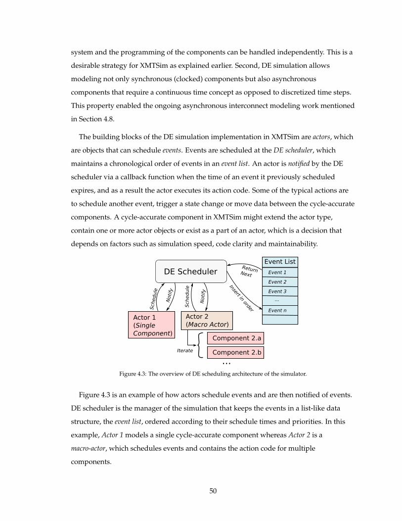
system and the programming of the components can be handled independently. This is a
desirable strategy for XMTSim as explained earlier. Second, DE simulation allows
modeling not only synchronous (clocked) components but also asynchronous
components that require a continuous time concept as opposed to discretized time steps.
This property enabled the ongoing asynchronous interconnect modeling work mentioned
in Section 4.8.
The building blocks of the DE simulation implementation in XMTSim are actors, which
are objects that can schedule events. Events are scheduled at the DE scheduler, which
maintains a chronological order of events in an event list. An actor is notified by the DE
scheduler via a callback function when the time of an event it previously scheduled
expires, and as a result the actor executes its action code. Some of the typical actions are
to schedule another event, trigger a state change or move data between the cycle-accurate
components. A cycle-accurate component in XMTSim might extend the actor type,
contain one or more actor objects or exist as a part of an actor, which is a decision that
depends on factors such as simulation speed, code clarity and maintainability.
DE Scheduler
Actor 1
(Single
Component)
Actor 2
(Macro Actor)
Component 2.a
Component 2.b
...
Schedule
Schedule
Noti
fy
Noti
fy
Iterate
Event List
Event 1
Event 2
Event 3
...
Event n
ReturnNext
Insert in order
Figure 4.3: The overview of DE scheduling architecture of the simulator.
Figure 4.3 is an example of how actors schedule events and are then notified of events.
DE scheduler is the manager of the simulation that keeps the events in a list-like data
structure, the event list, ordered according to their schedule times and priorities. In this
example, Actor 1 models a single cycle-accurate component whereas Actor 2 is a
macro-actor, which schedules events and contains the action code for multiple
components.
50

i n t time = 0 ;while ( t rue ) {
. . .i f ( . . . ) break ;time ++;
}
i n t time ;while ( t rue ) {
Event e = e v e n t L i s t . next ( ) ;time = e . time ( ) ;e . a c t o r ( ) . n o t i f y ( ) ;i f ( . . . ) break ;
}
(a) (b)
Figure 4.4: Main loop of execution for (a) Discrete-time simulation, (b) Discrete-event simulation.
It should be noted that XMTSim diverges from discrete-time(DT) architecture
simulators such as SimpleScalar [ALE02]. The difference is illustrated in Figure 4.4. The
DT simulation runs in a loop that polls through all the modeled components and
increments the simulated time at the end of each iteration. Simulation ends when a
certain criteria is satisfied, for example when a halt assembly instruction is encountered.
On the other hand, the main loop of the DE simulator handles one actor per iteration by
calling its notify method. Unlike DT simulation, simulated time does not necessarily
progresses at even intervals. Simulation is terminated when a specific type of event,
namely the stop event is reached. The advantages of the DE simulation were mentioned at
the beginning of this section. However, DT simulation may still be desirable in some
cases due to its speed advantages and simplicity in modeling small to medium sized
systems. Only the former is a concern in our case and we elaborate further on simulation
speed issues in Section 4.3.4.
A brief comparison of discrete-time versus discrete-event simulation is given in
Table 4.1. As indicated in the table, DT simulation is preferable for simulation of up to
mid-size synchronous systems, and the resulting code is often more compact compared to
the DE simulation code. For larger systems DT simulation might require an extensive
case study for ensuring correctness. Also, for the cases in which a lot of components are
defined but only few of them are active every cycle, DT simulation typically wastes
computation time on the conditional statements that do not fall through. Advantages of
DE simulation were discussed earlier in this section. Primary concern about DE
simulation is its performance, which may fall behind DT simulation as demonstrated in
the next section.
51

Table 4.1: Advantages and disadvantages of DE vs. DT simulation.
Discrete Time Simulation Discrete Event SimulationPros ·Efficient if a lot of work done for every ·Naturally suitable for an object-oriented structure
simulated cycle ·Can simulate asynchronous logic·More compact code for smaller ·More flexible in quantization of simulated timesimulations
Cons ·Requires complex case analysis for a ·Event list operations are expensivelarge simulator ·Might require more work for emulating one·Slow if not all components do work clock cycleevery clock cycle
4.3.2 Concurrent Communication of Data Between Components
In DE simulation, if the movement of data between various related components is
triggered by concurrent events, special care should be paid to ensure correctness of
simulation. As a result the DE simulation might require more work than DT simulation.
We demonstrate this statement on an example for simulating a simple pipeline. We first
show how the simulation is executed on a DT simulator, as it is the simpler case and then
move to the DE simulator.
Figure 4.5 illustrates how a 3 stage pipeline with a packet at each stage advances one
clock cycle in case of no stalls. Figure 4.5(a) is the initial status. Figures 4.5(b), 4.5(c) and
4.5(d) shows the steps that the simulation takes in order to emulate one clock cycle. In the
first step, the packet at the last stage (packet 3) is removed as the output. Then packets 2
and 1 are moved to the next stage, in that order. By starting at the end, it is ensured that
packets are not unintentionally overwritten.
Figure 4.6 shows the same 3 stage pipeline example of Figure 4.5 in DE simulation. We
assume that each stage of the pipeline is defined as an actor. For advancing the pipeline,
each actor will schedule an event at time T to pass its packet to the next stage. In DE
simulation, however, there is no mechanism to enforce an order between the notify calls
to the actors that schedule events for the same time (i.e., concurrent events). For example,
the actors can be notified in the order of stages 1, 2 and 3. As the figure exhibits, this will
cause accidental deletion of packets 2 and 3.
Figures 4.7 repeats the DE simulation but this time with intermediate storage for each
pipeline stage, which is denoted by smaller white boxes in Figures 4.7(b) and 4.7(c). For
this solution to work, we also have to incorporate the concept of priorities to the
52

1 2 3
1 2 3
1 2 3
1 2 3
(a) Initial State
(d) After 1
simulated cycle
(b)
(c)
Figure 4.5: Example of pipeline discrete time pipeline simulation.
simulation. We define two priorities, evaluate and update. The event list is ordered such
that evaluate events of a time instant in simulation come before the update events of the
same instant. In the example, at T-1 (initial state, Figure 4.7(a)) all actors schedule events
for T.evaluate. At the evaluate phase of T, T.evaluate (Figure 4.7.(b)), they move
packets to intermediate storage and schedule events for T.update. At the update phase
of T, T.update (Figure 4.7(c)), they pass the packets to the next stage.
Next, we compare the work involved in simulating the 3-stage pipeline in DT and DE
systems. In DT simulation, 3 move operations are performed to emulate one clock cycle.
In DE simulation, 6 move operations and 6 events are required. Clearly, DE simulation
would be slower in this example not only because of the number of move operations but
also the creation of events is expensive, since they have to be sorted when they are
inserted to the event list. This example supports the simulation speed argument in
Table 4.1.
53

1 2 3(a) Initial State
(d) End of simulated
cycle: packet 1 is
read as the output
(b) Stage 1 passes
package 1 to Stage 2 2 3
3
1
1
1(c) Stage 2 passes
package 1 to Stage 3
Figure 4.6: Example of discrete-event pipeline simulation. Simulation creates wrong output as the order ofnotify calls to actors cause packets to be overwritten.
1 2 3
1
(a) Time T-1:
Initial State
(b) Time T: After
evaluate phase2 31 2 3
1 2 31 2 3
(c) Time T: After
update phase. End
of simulated cycle.
Figure 4.7: Example of discrete-event pipeline simulation with the addition of priorities. Intermediate storageis used to prevent accidental deletion of packets.
4.3.3 Optimizing the DE Simulation Performance
As mentioned earlier, DT simulation may be considerably faster than DE simulation,
most notably when a lot of actions fall in the same exact moment in simulated time. A DT
simulator polls through all the actions in one sweep, whereas XMTSim would have to
54

schedule and return a separate event for each one (see Figure 4.4), which is a costly
operation. A way around this problem is grouping closely related components in one
large actor and letting the actor handle and combine events from these components. An
example is the macro-actor in Figure 4.3. A macro-actor contains the code for many
components and iterates through them at every simulated clock cycle. The action code of
the macro-actor resembles the DT simulation code in Figure 4.4a except the while loop is
replaced by a callback from the scheduler. This style is advantageous when the average
number of events that would be scheduled per cycle without grouping the components
(i.e., each component is an actor) passes a threshold. For a simple experiment conducted
with components that contain no action code, this threshold was 800 events per cycle. In
more realistic cases, the threshold would also depend on the amount of action code.
In XMTSim, clusters and shared caches are designed as macro-actors, as well as each of
the interconnection network (ICN) send and return paths. This organization not only
improves performance, it also facilitates maintainability of the simulator code and
provides the convenient means to replace any component by an alternative model, if
needed. We define the following mechanism to formalize the coding of macro-actors.
Ports: A macro-actor accepts inputs via its Port objects. Port is a Java interface class
which is defined by the two methods: (a) available(): returns a boolean value which
indicates that a port can be written to, (b) write(obj): accepts an object as its parameter,
which should be processed by the actor; can only be called if available method returns
true.
2-phase simulation: The phases refer to the priorities (evaluate and update) that were
defined in the previous section. The evaluate phase of a simulation instant is the set of all
events with evaluate priority at that instant. The update phase is defined similarly. Below
are the rules for coding a macro-actor within the 2-phase framework.
1. The available and write methods can only be called during the evaluate phase.
2. The output of the available method should be stable during the evaluate phase until
it is guaranteed that there will be no calls to the write method of the port.
3. The write method should not be called if a prior call to available for the same
simulation instant returns false.
55

4. If the write method of a port is called multiple times during the evaluate phase of a
simulation instant, it is not guaranteed that any of the writes will succeed. Typically
the write method should be called at most once for a simulation instant. However,
specific implementations of the Port interface might relax this requirement, which
should be noted in the API documentation for the class.
5. Typical actions of a macro-actor in the update phase are moving the inputs away
from its ports, updating the outputs of the available methods of the ports, and
scheduling the evaluate event for the next clock cycle (in XMTSim, evaluate phase
comes before the update phase). However, these actions are not requirements.
An example implementation of a MacroActor is given in Figure 4.8.
4.3.4 Simulation Speed
Simulation speed can be the bounding factor especially in evaluation of power and
thermal control mechanisms, as these experiments usually require simulation of relatively
large benchmarks. We evaluated the speed of simulation in throughput of simulated
instructions and in clock cycles per second on an Intel Xeon 5160 Quad-Core Server
clocked at 3GHz. The simulated configuration was a 1024-TCU XMT and for measuring
the speed, we simulated various hand-written microbenchmarks. Each benchmark is
serial or parallel, and computation or memory intensive. The results are averaged over
similar types and given in Table 4.2. It is observed that average instruction throughput of
computation intensive benchmarks is much higher than that of memory intensive
benchmarks. This is because the cost of simulating a memory instruction involves the
expensive interconnection network model. Execution profiling of XMTSim reveals that
for real-life XMTC programs, up to 60% of the time can be spent in simulating the
interconnection network. When it comes to the simulated clock cycle throughput, the
difference between the memory and computation intensive benchmarks is not as
significant, since memory instructions incur significantly more clock cycles than
computation instructions, boosting the cycle throughput.
56

c l a s s ExampleMacroActor extends Actor {// The only input port of the a c t o r . I t takes o b j e c t s of type// InputJob as input .Port <InputJob > inputPort ;
// Temporary s torage f o r the input j o b s passed via inputPort .InputJob inputPortIn , inputPortOut ;
// Constructor −− Contains the i n i t i a l i z a t i o n code f o r a new// o b j e c t of type ExampleMActor .ExampleMActor ( ) {
inputPort = new Port <InputJob > ( ) {publ ic void wri te ( InputJob job ) {
inputPort In = job ;// Upon r e c e i v i n g a new input , a c t o r should make sure// t h a t i t w i l l r e c e i v e a c a l l b a c k at the next update// phase . That code goes here .
}publ ic boolean a v a i l a b l e ( ) {
re turn inputPort In == n u l l ;}
}}
// Implementation of the c a l l b a c k funct ion ( c a l l e d by the scheduler ) .// Event o b j e c t t h a t caused the c a l l b a c k i s passed as a parameter .void not i fyActor ( Event e ) {
switch ( e . p r i o r i t y ( ) ) {case EVALUATE:
// Main a c t i o n code of the actor , which processes// inputPortOut . The a c t o r might wri te to the ports of// other a c t o r s . For example :// i f ( anotherActor . inputPort . a v a i l a b l e ( ) )// anotherActor . inputPort . wri te ( . . . )// Actor schedules next evaluate phase i f there i s more// work to be done .break ;
case UPDATE:i f ( inputPortOut == n u l l & inputPort In != n u l l ) {
inputPortOut = inputPort In ;inputPort In = n u l l ;
}// Here a c t o r schedules the next evaluate phase , i f there// i s more work to be done .// For example :// scheduler . schedule (new Event ( scheduler . time + 1 ) ,// Event .EVALUATE)break ;
}}
}
Figure 4.8: Example implementation of a MacroActor.
57

Table 4.2: Simulated throughputs of XMTSim.
Benchmark Group Instruction/sec Cycle/secParallel, memory intensive 98K 5.5KParallel, computation intensive 2.23M 10KSerial, memory intensive 76K 519KSerial, computation intensive 1.7M 4.2M
Table 4.3: The configuration of XMTSim that is used in validation against Paraleap.
Principal Computational Resources
Cores 8 TCUs in 8 clusters32-bit RISC ISA5 stage pipeline (4th stage may be shared and variable length)
Integer Units 64 ALUs (one per TCU), 8 MDUs and 8 FPUs (one each per cluster)On-chip Memory
Registers 8 KB integer and 8 KB FP (32 integer and 32 FP reg. per TCU)
Prefetch Buffers 1 KB (4 buffers per TCU)
Shared caches 256 KB total (8 modules, 32 KB each, 2-way associative, 8 word lines)
Read-only caches 512 KB (8 KB per cluster)
Global registers 8 registersOther
Interconnection Network (ICN) 8 x 8 Mesh-of-Trees
Memory controllers 1 controller, 32-b (1 word) bus width
Clock frequency ICN, shared caches and the cores run at the same frequency. Mem-ory controllers and DRAM run at 1/4 of the core clock to emulatethe core-to-memory controller clock ratio of the FPGA.
4.4 Cycle Verification Against the FPGA Prototype
We validated the cycle-accurate model of XMTSim against the 64-core FPGA XMT
prototype, Paraleap. The configuration of XMTSim that matches Paraleap is given in
Table 4.3. In addition to serving as a proof-of-concept implementation for XMT, Paraleap
was also set up to emulate the operation of a 800MHz XMT computer with a DDR
DRAM. The clock of the memory controller was purposefully slowed down so that its
ratio to the core clock frequency matches that of the emulated system. The simulator
configuration reflects this adjustment.
Even though XMTSim was based on the hardware description language description of
Paraleap, discrepancies between the two exist:
• Due to its development status, certain specifications of Paraleap does not exactly
match those of the envisioned XMT chip modeled by XMTSim. Given the same
58

amount of effort and on-chip resources that are put towards an industrial grade
ASIC product (as opposed to a limited FPGA prototype), these limitations would
not exist. Some examples are:
– Paraleap is spread over multiple FPGA chips and requires additional buffers at
the chip boundaries which add to the ICN latency. These buffers are not
necessary for modeling an ASIC XMT chip, and are not included in XMTSim.
– Due to die size limitations, Paraleap utilizes a butterfly interconnection
network instead of the MoT used in XMTSim.
– The sleep-wake mechanism proposed in Section 3.5 is implemented in
XMTSim but not in Paraleap.
• Our experiences show that some implementation differences do not cause a
significant cycle-count benefit or penalty however their inclusion in the simulator
would cause code complexity and slow down the simulation significantly (as well
as requiring a considerable amount of development effort). Note that, one of the
major purposes of the XMT simulator is architectural exploration and therefore the
simulation speed, code clarity, modularity, self documentation and extensibility are
important factors. Going into too much detail for no clear benefit conflicts with
these objectives. For example, some of the cycle-accurate features of the Master
TCU are currently under development. The benchmarks that we use in our
experiments usually have insignificant serial sections therefore the inefficiencies of
the master TCU should not effect simulation results significantly.
• An accurate external DRAM model, DRAMSim, is currently being incorporated to
XMTSim [WGT+05]. Meanwhile XMTSim does models DRAM communication as
constant latency.
• Currently XMT does not feature an OS, therefore I/O operations such as printf’s
and file operations cannot be simulated in a cycle-accurate way.
Another difficulty in validating XMTSim against Paraleap is related to the
indeterminism in the execution of parallel programs. A parallel program can take many
execution paths based on the order of concurrent reads or writes (via prefix-sum or
59

Table 4.4: Microbenchmarks used in cycle verification
CyclesName Description Paraleap XMTSim Diff.
MicrPar0 Start 1024 threads and for each thread run a 50000 iterationloop with a single add instruction in it.
1600513 1600327 <1%
MicrPar1 Start 102400 threads and for each thread issue a sw instructionto address 0.
204943 204918 <1%
MicrPar2 Start 1024 threads and for each thread run a 18000 iterationloop with an add and a mult instruction in it.
3456482 3456318 <1%
MicrPar3 Start 1024 threads and for each thread run a 150 iteration loopwith an add and a sw to address 0 instruction in it.
307349 307710 <1%
MicroPar4 Start 1024 threads and for each thread run a 1800 iteration loopwith a sw instruction (and wrapper code) in it. Sw instruc-tions from different TCUs will be spread across the memorymodules.
935225 626908 -33%
MicroPar5 Start 1024 threads and for each thread run a 10K iteration loopwith an add, a mult and a divide instruction in it.
8320486 8320318 <1%
MicroSer6 Measure the time to execute a starting and termination of200K threads.
6226029 4587533 -26%
memory operations in XMT). If the program is correct it is implied that all these paths
will give correct results, however the cycle or assembly instruction count statistics will
not necessarily match between different paths. The order of these concurrent events is
arbitrary and there is no reliable way to determine if Paraleap and XMTSim will take the
same paths if more than one path is possible. For this reason, a benchmark used for
validation purposes should guarantee to yield near identical cycle and instruction counts
for different execution paths.
Table 4.4 lists the first set of micro-benchmarks we used in verification. Each
benchmark is hand-coded in assembly language for stressing a different component of
the parallel TCUs as described in the table. The difference in cycle counts is calculated as
Difference =(CY Csim − CY Cfpga)
CY Cfpga× 100 (4.1)
where CY Csim and CY Cfpga are the cycle counts obtained on the simulator and Paraleap,
respectively. These benchmarks fulfill the determinism requirement noted earlier and the
only significant deviation in cycle counts is observed for the MicroPar4 benchmark
(33%). This deviation can be explained by the differences between the interconnect
structures of XMTSim and Paraleap as mentioned above.
60

4.5 Power and Temperature Estimation in XMTSim
Power and temperature estimation in XMTSim is implemented using the activity plug-in
mechanism. (The activity plug-in mechanism was first mentioned in Section 4.2).
XMTSim contains a power-temperature (PTE) plug-in for a 1024 TCU configuration by
default. We explain how we compute the power model parameters for this configuration
later in Chapter 6. Other configurations can easily be added, however power model
parameters should also be created for the new configurations.
As the thermal model, we incorporated HotSpot1. HotSpot is written in the C language
and in order to make it available to XMTSim we created HotSpotJ, a Java Native Interface
(JNI) [Lia99] wrapper for HotSpot. HotSpotJ is available as a part of XMTSim but it is also
a standalone tool and can be used with any Java based simulator. We extended HotSpotJ
with a floorplan tool, FPJ, that we use as an interface between XMTSim and HotSpotJ. FPJ
is essentially a hierarchical floorplan creator, in which the floorplan blocks are
represented as Java objects. A floorplan is created using the FPJ interface and passed to
the simulator at the beginning of the simulation. During the simulation it is used as a
medium to pass power and temperature data of the floorplan blocks between XMTSim
and HotSpotJ. More information on HotSpotJ (and FPJ) will be given in Appendix C.
Figure 4.9 illustrates the working of XMTSim with the PTE plug-in. Steps of estimation
for one sampling interval are indicated on the figure. XMTSim starts execution by
scheduling an initial event for a callback to the PE plug-in. When the PE plug-in receives
the callback, it interacts with the activity trace interface to collect the statistics that will be
explained in the next section and resets the associated counters. Then, it converts these
statistics, also called activity traces, to power consumption values according to the power
model. It sets the power of each floorplan module on the floorplan object and passes it to
HotSpotJ. HotSpotJ computes temperatures for the modules. Finally, the PTE plug-in
schedules the next callback from the simulator. Users can create their own plug-ins with
models other than the one that we will explain next, as long as the model can be
described in terms of the statistics reported by the activity trace interface.
1HotSpot [HSS+04, HSR+07, SSH+03] was previously mentioned in Section 2.10
61

XMTSimActivity
Trace
InterfacePower
Estimation Plug-in
1. Callback for power
estimation
2. Read counters from
components and
reset counters
6. Schedule next
callback
Power Model
3. Pass activity values
HotSpotJ
4. Set power on floorplan
modules and pass to HotSpotJ
5. Report
temperature.
Figure 4.9: Operation of the power/thermal-estimation plug-in.
4.5.1 The Power Model
For the power model of XMTSim, we combine the models explained in Sections 2.2.2
and 2.3.2 to fit them into the framework proposed by Martonosi and Isci [IM03].
According to their model, the simulation provides the access rate for each component
(Ci), which is a value between 0 and 1. The power of a component is a linear function of
the access rate with a constant offset.
Power(Ci) =AccessRate(Ci) ·
MaxActPower(Ci) + (4.2)
Const(Ci)
C is the set of microarchitectural components for which the power is estimated. We
will give the exact definition of AccessRate(Ci) shortly. MaxActPower(Ci) is the upper
bound on the power that is proportional to the activity and Const(Ci) is the power of a
component which is spent regardless of its activity.
According to Sections 2.2.2 and 2.3.2, the total power of a component, which is the sum
of its dynamic power (Equation (2.4)) and leakage power (Equation (2.6)), is expressed as:
P = Pdyn,max ·ACT · CF +DUTYclk · Pdyn,max · (1− CF ) +DUTYV · Pleak,max (4.3)
62

The configuration parameters in the simulation are Pdyn,max and Pleak,max, which are
the maximum dynamic and leakage powers and CF, which is the activity correlation
factor.
ACT is identical to AccessRate(Ci) above, which is the average activity of a the
component for the duration of the sampling period and obtained from simulation.
XMTSim utilizes internal counters that monitor the activity of each architectural
component. We will discuss the definition of activity on a per component basis in the
remainder of this section. DUTYclk and DUTYV are the clock and voltage duty cycles,
which were explained in Sections 2.2.2 and 2.3.2. Note that DUTYV is always greater than
DUTYclk since voltage gating implies that clock is also stopped.
If we assume that no voltage gating or coarse grain clock gating is applied (i.e., both
duty cycles are 1), Equation (4.3) can be simplified to:
P = Pdyn,max ·ACT · CF + Pdyn,max · (1− CF ) + Pleak,max (4.4)
In this form, the Pdyn,max ·ACT · CF and the Pdyn,max · (1− CF ) + Pleak,max terms are
the equivalents of MaxActPower(Ci) and Const(Ci) in Equation (4.2), respectively.
If CF is less than 1, Const(Ci) not only contains the leakage power but, also contains a
part of the dynamic power. A common value to set the activity correlation factor (CF ) for
aggressively fine-grained clock gated circuits is 0.9, which is the same assumption as
Wattch power simulator [BTM00] uses.
Next, we provide details on the activity models of the microarchitectural components
in XMTSim. As we discussed in Section 2.10, parameters required to convert the activity
to power values can be obtained using tools such as McPAT 0.9 [LAS+09] and Cacti
6.5 [WJ96, MBJ05].
Computing Clusters. The power dissipation of an XMT cluster is calculated as the sum
of the individual elements in it, which are listed below: The access rate of a TCU pipeline
is calculated according to the number of instructions that are fetched and executed, which
is a simple but sufficiently accurate approximation. For the integer and floating point
units (including arbitration), access rates are the ratio of their throughputs to the
63

maximum throughput. The remainder of the units are all memory array structures and
their access rates are computed according to the number of reads and writes they serve.
Memory Controllers, DRAM and Global Shared Caches. The access rate of these
components are calculated as the ratio of the requests served to the maximum number of
requests that can be served over the sampling period (i.e. one request per cycle).
Global Operations and Serial Processor. We omit the power spent on global
operations, since the total gate counts of the circuits that perform these operations were
found to be insignificant with respect to the other components, and these operations
make up a negligible portion of execution time. In fact, prefix-sum operations and global
register file accesses make up less than 1.5% of the total number of instructions among all
the benchmarks. We also omit the power of the XMT serial processor, which is only active
during serial sections of the XMTC code and when parallel TCUs are inactive. None of
our benchmarks contain significant portions of serial code: the number of serial
instructions, in all cases, is less than 0.005% of the total number of instructions executed.
Interconnection Network The power of the Mesh-of-Trees (MoT) ICN includes the
total cost of communication from all TCUs to the shared caches and back. The access rate
for the ICN is equal to its throughput ratio, which is the ratio of the packets transferred
between TCUs and shared caches to the maximum number of packets that can be
transferred over the sampling period.
The power cost of the ICN can be broken into various parts [KLPS11], which fit into the
framework of Equation (4.2) in the following way. The power spent by the reading and
writing of registers, and the charge/discharge of capacitive loads due to wires and
repeater inputs can be modeled as proportional to the activity (i.e. number of transferred
packets). All packets travel the same number of buffers in the MoT-ICN, and the wire
distance they travel can be approximated as a constant which is the average of all possible
paths. The power of the arbiters is modeled as a worst-case constant, as it is not feasible
to model it accurately in a fast simulator.
The power of the interconnection network (ICN) is a central theme in Section 6.4, which
will explore various scenarios considering possible estimation errors in the power model.
64

XMTSimActivity
Trace
Interface DPTM Plug-in
1. Callback for DPTM
2. Read counters from
components and
reset counters
7. Schedule next
callback
Power Model
3. Pass activity values
HotSpotJ
4. Set power on floorplan
modules and pass to HotSpotJ
5. Report
temperature.
DPTM Algorithm
Clock
Frequency
Interface
6. Modify clocks
Figure 4.10: Operation of a DTM plug-in.
4.6 Dynamic Power and Thermal Management in XMTSim
Dynamic Power and Thermal Management (DPTM) in XMTSim works in a similar way
to the PTE plug-in with the addition of a DPTM algorithm stage. The DPTM algorithm
changes the clock frequencies of the microarchitectural blocks in reaction to the state of
the simulated chip with respect to the constraints.
Figure 4.10 shows the changes to the PTE plug-in. The two mechanisms are identical
up to step 5, at which point the PTE plug-in finishes the sampling period, while the
DPTM plug-in modifies the clocks according to the chosen algorithm. The clocks are
modified via the standardized API of the clocked components.
4.7 Other Features
In this section we will summarize some of the additional features of XMTSim.
Execution traces. XMTSim generates execution traces at various detail levels. At the
functional level, only the results of executed assembly instructions are displayed. The
more detailed cycle-accurate level reports the components through which the instruction
and data packets travel. Traces can be limited to specific instructions in the assembly
input and/or to specific TCUs.
Floorplan visualization. The FPJ package of the HotSpotJ tool can be used for
purposes other than interfacing between XMTSim and HotSpotJ. The amount of
simulation output can be overwhelming, especially for a configuration that contains
65

many TCUs. FPJ allows displaying data for each cluster or cache module on an XMT
floorplan, in colors or text. It can be used as a part of an activity plug-in to animate
statistics obtained during a simulation run. Example outputs from FPJ can be found in
Chapter 7 (for example, Figure 7.8). FPJ is explained in further detail in Appendix C.
Checkpoints. XMTSim supports simulation checkpoints, i.e., the state of the
simulation can be saved at a point that is given by the user ahead of time or determined
by a command line interrupt during execution. Simulation can be resumed at a later time.
This is a feature which, among other practical uses, can facilitate dynamically load
balancing a batch of long simulations running on multiple computers.
4.8 Features under Development
XMTSim is an experimental tool that is under active development and as such, some
features and improvements either currently being tested or they are in its future roadmap.
More accurate DRAM model. As mentioned earlier, an accurate external DRAM
model, DRAMSim, is currently being incorporated to XMTSim [WGT+05].
Phase sampling. Programs with very long execution times usually consist of multiple
phases where each phase is a set of intervals that have similar behavior [HPLC05]. An
extension to the XMT system can be tested by running the cycle-accurate simulation for a
few intervals on each phase and fast-forwarding in-between. Fast-forwarding can be
done by switching to a fast mode that will estimate the state of the simulator if it were run
in the cycle-accurate mode. Incorporating features that will enable phase sampling will
allow simulation of large programs and improve the capabilities of the simulator as a
design space exploration tool.
Asynchronous interconnect. Use of asynchronous logic in the interconnection
network design might be preferable for its advantages in power consumption. Following
up on [HNCV10], work in progress with our Columbia University partner compares the
synchronous versus asynchronous implementations of the interconnection network
modeled in XMTSim.
66

Increasing simulation speed via parallelism. The simulation speed of XMTSim can be
improved by parallelizing the scheduling and processing of discrete-events [Fuj90]. It
would also be intriguing to run XMTSim as well as the computation hungry simulation of
the interconnection network component on XMT itself. We are exploring both.
4.9 Related Work
Cycle-accurate architecture simulators are particularly important for evaluating the
performance of parallel computers due to the great variation in the systems that are being
proposed. Many of the earlier projects simulating multi-core processors extended the
popular uniprocessor simulator, SimpleScalar [ALE02]. However, as parallel architectures
started deviating from the model of simply duplicating serial cores, other
multi/many-core simulators such as ManySim [ZIM+07], FastSim [CLRT11] and
TPTS [CDE+08] were built. XMTSim differs from these simulators, since it targets shared
memory many-cores, a domain that is currently underrepresented. GPU simulators,
Barra [SCP09], Ocelot [KDY09] and GPGPUSim [BYF+09] are closer to XMTSim in the
architectures that they simulate but they are limited by the programming models of these
architectures. Also, Barra and Ocelot are functional simulators, i.e., they do not report
cycle-accurate measures. Kim, et al extended Ocelot with a power model, however it is
not possible to simulate dynamic power and thermal management with this system.
Cycle-accurate architecture simulators can also be built on top of existing simulation
frameworks such as SystemC. An example is the simulator presented by Lebreton, et
al. [LV08]. Instead, we chose to build our own infrastructure since XMTSim is intended as
a highly configurable simulator that serves multiple research communities. Our
infrastructure gives us the flexibility to incorporate second party tools, for example
SableCC [GH98], which is the front end for reading the input files. In this case, SableCC
enabled easy addition of new assembly instructions as needed by user’s of XMTSim.
Simulation speed is an issue, especially in evaluating thermal management. Atienza, et
al. [AVP+06] presented a hardware/software framework that featured an FPGA for fast
simulation of a 4-core system. Nevertheless, it is not feasible to fit a 1024-TCU XMT
processor on the current FPGAs.
67

Chapter 5
Enabling Meaningful Comparison of XMT with Contemporary
Platforms
In the previous chapters, we discussed the XMT architecture and introduced its
cycle-accurate simulator. In this chapter, we first enable a meaningful comparison of XMT
with contemporary industry platforms by establishing a hardware configuration of XMT
that is silicon area-equivalent of a modern many-core GPU, NVIDIA GTX2801 [NVIa].
Then, using the simulator, we compare the runtime performance of the two processors on
a range of irregular and regular parallel benchmarks (see Section 5.3 for definitions of
regular and irregular). The 1024-TCU XMT configuration (XMT1024) we present here is
employed in the following chapters and the comparison against GTX280, besides
demonstrating the performance advantages of XMT, also confirms that those chapters
target a realistic XMT platform.
The highlights of this work are:
• A meaningful performance comparison of a state-of-the-art GPU to XMT, a
general-purpose highly parallel architecture, on a range of both regular and
irregular benchmarks. We show via simulation that XMT can outperform GPUs on
irregular applications, while not falling behind significantly on regular
benchmarks.
• Beyond the specific comparison to XMT, the results demonstrate that an easy to
program, truly general-purpose architecture can challenge a performance-oriented
architecture – a GPU – once applications exceed a specific scope of the latter.
In the course of this chapter we list the specifications for an XMT processor
area-equivalent to the GTX280 GPU, configure and use XMTSim to simulate the
envisioned XMT processor, collect results from simulations and compare them against the
1At the time of the writing GTX280 was the most advanced commercially available GPU.
68

results from the GPU runs. Preparations of the XMT and the GPU benchmarks for this
work and the compiler optimizations for improving XMT performance were the topic of
another dissertation [Car11]. The analysis of the results was a collaboration between the
two dissertation projects.
The organization of this chapter is as follows. In Section 5.1, we review NVIDIA Tesla,
the architecture of the GTX280 GPU, and compare its high level design specifications with
those of XMT. In Section 5.2, we present a configuration of XMT that is feasible to
implement, in terms of silicon area, using current technology. In section 5.3, we introduce
the benchmarks used to perform the comparison. Finally, in Section 5.4 we report the
performance comparison data.
5.1 The Compared Architecture – NVIDIA Tesla
In this section, we go over the NVIDIA Tesla architecture, and the CUDA programming
environment and compare it against the XMT architecture. We start by explaining the
importance of the GPU platform.
GPUs are the main example of many-cores that are not typically confined to traditional
architectures and programming models, and use hundreds of lightweight cores in order
to provide better speedups. In this respect, they are similar to the design of XMT.
However, GPUs perform best on applications with very high degrees of parallelism; at
least 5,000 – 10,000 threads according to [SHG09], whereas XMT parallelism scales down
to provide speedups for programs with only a few threads.
Advances in GPU programming languages (CUDA by GPU vendor,
NVIDIA [NBGS08], Brook by AMD [BFH+04], and the upcoming OpenCL
standard [Mun09]) and architecture upgrades have led to strong performance
demonstrated for a considerable range of software. When all optimizations are applied
correctly by the programmer, GPUs provide remarkable speedups for certain types of
applications. As of January 2010, the NVIDIA CUDA Zone website [NVI10] lists 198
CUDA applications, 28 of which reporting speedups of 100× or more. On the other hand,
the programming effort required to extract performance can be quite significant. The fact
that the implementation of basic algorithms on GPUs, such as sorting, merit so many
69

...
...
...
StreamingMultiproc.
SharedMemory
Interconnection Network
DRAM
Register File
Warp SchedulerWarp State
InstructionCache
ConstantCache
SP
SpecialFunction
Unit (SFU)
SP
SP
SP
Shared Memory
Thread Block Scheduler
SP SP
SP SP
...
...
Texture Cache
SpecialFunction
Unit (SFU)
TextureCache
Load/StoreUnit
Controler
DRAM
Texture Cache
Controler
StreamingMultiproc.
SharedMemory
SP SP
SP SP...
Figure 5.1: Overview of the NVIDIA Tesla architecture.
research papers (e.g., [BG09, CT08, SA08]) affirms that. Nevertheless, the notable
performance benefits led some researchers to regard GPUs as the most promising
solution for the pervasive computing platform of the future. The emergence of
General-Purpose GPU (GPGPU) communities is perhaps one indication of this belief.
5.1.1 Tesla/CUDA Framework
In recent years, GPU architectures have evolved from purely fixed-function devices to
increasingly flexible, massively parallel programmable processors. The
CUDA [NBGS08, NVI09] programming environment together with the NVIDIA
Tesla [LNOM08] architecture is one example of a GPGPU system gaining acceptance in
the parallel computing community.
Fig. 5.1 depicts an overview of the Tesla architecture. It consists of an array of
Streaming Multiprocessors (SMs), connected through an interconnection network to a
number of memory controllers and off-chip DRAM modules. Each SM contains a shared
register file, shared memory, constant and instruction caches, special function units and
several Streaming Processors (SPs) with integer and floating point ALU pipelines. SFUs
are 4-wide vector units that can handle complex floating point operations. The CUDA
programming and execution model are discussed elsewhere [LNOM08].
A CUDA program consists of serial parts running on the CPU, which call parallel
kernels offloaded to a GPU. A kernel is organized as a grid (1, 2 or 3-dimensional) of
thread blocks. A thread block is a set of concurrent threads that can cooperate among
70

themselves through a block-private shared memory and barrier synchronization.
A global scheduler assigns thread blocks to SMs as they become available. Thread
blocks are partitioned into fixed-size warps (e.g. 32 threads); At each instruction issue
time, a scheduler selects a fixed-size warp (32 threads) that is ready to execute and issues
the next instruction to all the threads in the warp. Threads proceed in lock-step manner,
and this execution model is called SIMT – Single Instruction Multiple Threads.
The CUDA framework provides a relatively familiar environment for developers,
which led to an impressive number of applications to be ported since its
introduction [NVI10]. Nevertheless, a non-trivial development effort is required when
optimizing an application in the CUDA model. Some of the considerations that must be
addressed in order to get significant performance gains are:
Degree of parallelism: A minimum of 5,000 - 10,000 threads need to be in-flight for
achieving good hardware utilization and latency hiding.
Thread divergence: In the CUDA Single Instruction Multiple Threads (SIMT) model,
divergent control flow between threads causes serialization, and programmers are
encouraged to minimize it.
Shared memory: No standard caches are included at the SMs. Instead, a small
user-controlled scratch-pad shared memory per SM is provided, and these memories are
subject to bank conflicts that limit the performance if the references are not properly
optimized. SMs also feature constant and texture caches but these memories are
read-only and use separate address spaces.
Memory request coalescing: better bandwidth utilization is achieved when data
layout and memory requests follow a number of temporal and spatial locality guidelines.
Bank conflicts: concurrent requests to one bank of the shared memory incur
serialization, and should be avoided in the code, if possible.
5.1.2 Comparison of the XMT and the Tesla Architectures
The key issues that affect the design of the XMT and the Tesla architectures, and the main
differences between them, are summarized in Table 5.1.
71

The fundamental difference between the Tesla and the XMT architectures is their target
applications. GPUs such as Tesla aim to provide high peak performance for regular
parallel programs, given that they are optimized using the specific guidelines provided
with the programming model. For example, global memory access patterns need to be
coordinated for high interconnect utilization and scratchpad memory accesses should be
arranged to not cause conflicts on memory banks. However, GPUs can yield suboptimal
performance for low degrees of parallelism and irregular memory access patterns.
XMT is designed for high performance on workloads that fall outside the realm of
GPUs. XMT excels on programs that show irregular parallelism patterns, such as control
flow that diverges between threads or irregular memory accesses. XMT also scales down
well on programs with low degrees of parallelism. Hence, the specifications of XMT are
not geared towards high peak performance. However, as we will see in following
sections, XMT still does not fall behind on regular programs in a significant way.
72

Tesl
aX
MT
Mem
ory
Late
ncy
Hid
ing
and
Red
uctio
n
•H
eavy
mul
tith
read
ing
(req
uire
sla
rge
regi
ster
files
and
stat
eaw
are
sche
dule
r).
•Li
mit
edlo
cals
hare
dsc
ratc
hpad
mem
ory.
•N
oco
here
ntpr
ivat
eca
ches
atSM
orSP
.
•La
rge
glob
ally
shar
edca
che.
•N
oco
here
ntpr
ivat
eTC
Uor
clus
ter
cach
es.
•So
ftw
are
pref
etch
ing.
Mem
ory
and
Cac
heBa
ndw
idth
•M
emor
yac
cess
patt
erns
need
tobe
coor
dina
ted
byth
eus
erfo
ref
ficie
ncy
(req
uest
coal
esci
ng).
•Sc
ratc
hpad
mem
orie
spr
one
toba
nkco
nflic
ts.
•H
igh
band
wid
thin
terc
onne
ctio
nne
twor
k.
•C
ache
sre
lax
the
need
for
user
-coo
rdin
ated
DR
AM
acce
ss.
•A
ddre
ssha
shin
gfo
rav
oidi
ngm
emor
ym
odul
eho
tspo
ts.
•M
esh-
of-t
rees
inte
rcon
nect
able
toha
ndle
irre
gula
rco
mm
unic
atio
nef
ficie
ntly
.
Func
tiona
lUni
t(F
U)A
lloca
tion
•D
edic
ated
FUs
for
SPs
and
SFU
s.
•Le
ssar
bitr
atio
nlo
gic
requ
ired
.
•H
ighe
rth
eore
tica
lpea
kpe
rfor
man
ce.
•H
eavy
wei
ghtF
Us
(FPU
/MD
U)a
resh
ared
thro
ugh
arbi
trat
ors.
•Li
ghtw
eigh
tFU
s(A
LUan
dbr
anch
unit
)are
allo
cate
dpe
rTC
U(A
LUs
dono
tinc
lude
mul
tipl
y/di
vide
func
tion
alit
y).
Con
trol
Flow
and
Sync
hron
izat
ion
•Si
ngle
inst
ruct
ion
cach
ean
dis
sue
per
SMfo
rsa
ving
reso
urce
s.W
arps
exec
ute
inlo
ck-s
tep
(pen
aliz
esdi
verg
ing
bran
ches
).
•Ef
ficie
ntlo
cals
ynch
roni
zati
onan
dco
mm
unic
atio
nw
ithi
nbl
ocks
.Glo
bal
com
mun
icat
ion
isex
pens
ive.
•Sw
itch
ing
betw
een
seri
alan
dpa
ralle
lmod
es(i
.e.,
pass
ing
cont
rolf
rom
CPU
toG
PU)
requ
ires
off-
chip
com
mun
icat
ion.
•O
nein
stru
ctio
nca
che
and
prog
ram
coun
ter
per
TCU
enab
les
inde
pend
entp
rogr
essi
onof
thre
ads.
•C
oord
inat
ion
ofth
read
sca
nbe
perf
orm
edvi
aco
nsta
ntti
me
prefi
x-su
m.O
ther
form
sof
thre
adco
mm
unic
atio
nar
edo
neov
erth
esh
ared
cach
e.
•D
ynam
icha
rdw
are
supp
ortf
orfa
stsw
itch
betw
een
seri
alan
dpa
ralle
lmod
esan
dlo
adba
lanc
eof
virt
ualt
hrea
ds.
Tabl
e5.
1:Im
plem
enta
tion
diff
eren
ces
betw
een
XM
Tan
dTe
sla.
FPU
and
MD
Ust
and
for
float
ing-
poin
tand
mul
tipl
y/di
vide
unit
sre
spec
tive
ly.
73

5.2 Silicon Area Feasibility of 1024-TCU XMT
In this section, we aim to establish a configuration of XMT that is feasible to implement,
in terms of silicon area, using current technology. The issue of power is investigated
separately in Chapter 6. Since we would like to compare the performance of XMT against
the GTX280 GPU (see Section 5.4), we assume that a 576mm2 die, which is the area of
GTX280, is also available to us in 65 nm ASIC technology.
We start the section with information on the ASIC implementation of the 64-TCU XMT
prototype. This is followed by the area estimation of a 1024-TCU XMT processor
configuration (XMT1024), complete with number of TCUs, functional units, shared cache
size, and interconnection network (ICN) specifications. The area estimation includes a
subsection that contains the details, such as dimensions of modules, required for
constructing the XMT1024 floorplan in Section 7.3.
5.2.1 ASIC Synthesis of a 64-TCU Prototype
The 64-TCU integer-only 200MHz XMT ASIC prototype, fabricated in 90 nm IBM
technology, serves the dual purpose of constituting a proof-of-concept for XMT and
providing the basis for the area estimation of clusters and shared caches (see Table 5.4)
presented in the remainder of this section. The power data obtained from the gate level
simulations is also utilized in Section 6.1.
The ASIC prototype was a collaborative effort among the members of the XMT
research team including the author of this dissertation. We used the post-layout area
reported in 90 nm technology for projecting the area of the XMT1024 chip.
Synopsys [Syn] and Cadence [Cad] logic synthesis, place and route, physical verification
and gate level simulation tools were used for the tape-out.
5.2.2 Silicon Area Estimation for XMT1024
We needed to determine the power-of-two configuration of XMT, the chip resources of
which are in the same ballpark as the GTX280. We base our estimation on the detailed
data from the ASIC implementation of the MoT interconnection
74

network [BQV08, BQV09, Bal08] and the 64-TCU ASIC prototype. Our calculations below
show that using the same generation technology as the GTX280, a 1024-TCU XMT
configuration could be fabricated.
Overview and Intuition
A 1024-TCU XMT configuration requires 16 times the cluster and cache modules
resources of the 64-TCU XMT ASIC prototype, reported by the design tools as 47 mm2.
The area of the MOT interconnection network for the envisioned XMT configuration can
be estimated as 170 mm2 in 90nm using the data from [Bal08]. Applying a theoretical area
scaling factor of 0.5 from 90nm to 65nm technology feature size we obtain an area
estimate of (47× 16 + 170)× 0.5 = 461mm2. We assume that with the same amount of
engineering and optimization effort put behind it as for the GPUs, XMT could support a
comparable clock frequency and addition of floating point units (whose count, per Table
5.2, is around 20% of the GTX 280) without a significant increase in area budget. This is
why the XMT clock frequency considered in the comparison is the same as the shader
clock frequency (SPs and SFUs) of GTX280, which is 1.3GHz. Note that this estimation
does not include the cost of memory controllers. The published die area of GTX280 is
576mm2 in 65nm technology and approximately 10% of this area is allocated for memory
controllers [Kan08]. It is reasonable to assume that the difference in the GPU area and the
estimated XMT area, which is also approximately 20%, would account for the addition of
the same number of controllers to XMT. We expect that very limited area will be needed
for XMT beyond the sum of these components since they comprise a nearly full design.
Table 5.2 gives a comparative summary of the hardware specifications of an NVIDIA
GTX280 and the simulated XMT configuration. The sharp differences in this table are due
to the different architectural design decisions summarized in Table 5.1. From these
calculations, we conclude that overall, the configurations of these very different
architectures appear to use roughly the same amount of resources.
Detailed Area Estimation
Clusters, cache modules and the ICN are the components that take up the majority of the
die area in an XMT chip. In this section, we will project their dimensions in 65nm
technology based on our 90nm ASIC prototype implementation reviewed in Section 5.2.1.
75

GTX280 XMT-1024
Principal Computational ResourcesCores 240 SP, 60 SFU 1024 TCUInteger Units 240 ALU+MDU 1024 ALU, 64 MDUFloating Point Units 240 FPU, 60 SFU 64 FPU
On-chip MemoryRegisters 1920KB 128KBPrefetch Buffers – 32KBRegular caches 480KB 4104KBConstant cache 240KB 128KBTexture cache 480KB –
Other ParametersPipeline clk. freq. 1.3 GHz 1.3 GHzInterconnect clk. freq. 650 MHz 1.3 GHzVoltage ? 1.15VBandwidth to DRAM 141.7 GB/sec (peak theoretical)Fab. technology 65 nmSilicon area 576 mm2
Table 5.2: Hardware specifications of the GTX280 and the simulated XMT configuration. In each category, theemphasized side marks the more area-intensive implementation. Values that span both columns are commonto GTX280 and XMT1024. GTX280 voltage was not listed in any of the sources.
Table 5.3: The detailed specifications of XMT1024.
Processing Clusters·64 clusters x 16 TCUs·In-order 5–stage pipelines·2-bit branch prediction·16 prefetch buffers per TCU·64 MDUs, 64 FPUs·2K read-only cache per cluster
Interconnection Network·64-to-128 Mesh-of-Trees
Shared Parallel Cache·128 modules x 32K (4MB total)·2-way associative
76

Module Area in 95 nm Area estimated for 65 nm Total Area for all Modules
Cluster 2× 3.6 = 7.2mm2 7.2× 0.5× 1.1 = 3.96mm2 3.96× 64 = 253.4mm2
Cache 1.33× 1.7 = 2.26mm2 2.26× 0.5× 1.1 = 1.24mm2 1.24× 128 = 159.1mm2
ICN 26.3 + 5.2 = 31.5mm2 [26.3× ( 5234 × 0.7)2 + 5.2× 5234 × 0.5]× 1.25× 2 = 85.2mm2
Total 497.7mm2
Table 5.4: The area estimation for a 65 nm XMT1024 chip.
Table 5.3 lists the specifications of XMT1024 in detail and the calculations that lead to
the estimate of the total chip area are summarized in Table 5.4. For clusters and caches,
we start with the dimensions measured post-layout in 90nm. Cluster dimensions are
2mm× 3.6mm, and for cache module dimensions are 1.33mm× 1.7mm. We apply a
factor of 0.5 for estimating the area in the 65nm technology node (see Section 2.7 for area
scaling between technology nodes). In future implementations of the XMT processor (ex.,
XMT1024), design of the clusters and the caches is not anticipated to change significantly.
We only foresee inclusion of floating point capability in clusters (only single-precision for
the purposes of this work). Area optimization was not an objective for the prototype, we
predict that an aggressively optimized cluster design would be able to accommodate the
addition of a floating point unit within the same area. Moreover, the place-and-route
results showed that the space within the cluster bounding box was not fully utilized. To
be on the safe side, we add a 10% margin to the area of clusters and cache modules (the
1.1 multiplier in column 3 of the table), which could compensate further for the floating
point unit and also for internal interconnect routing costs expected for a larger system.
The last column of the table gives the total area for 64 clusters and 128 cache modules.
The area of the interconnection network is estimated based on the work in [Bal08],
which reports the area of a 64 terminal 34-bit ICN in 95 nm. The total logic cell area was
found to be 26.3mm2 and the wire area was 5.2mm2. The area of a different
configuration can be estimated using the following relation (see [Bal08]):
Wire area ∝ (wc · dw)2 (5.1)
Cell area ∝ wc · k
77

where wc is the bit count, dw is wire pitch (95nm and 65nm) and k is the transistor feature
size (65nm, 95nm, etc.). Another factor that could increase the ICN area is the inclusion of
repeaters. Repeaters are added in order to satisfy the timing constraints for high clock
frequencies. In [Bal08], it was reported that the area overhead of repeaters for a 16
terminal ICN to attain a clock frequency of 1GHz is 5% and for 32 terminals, the overhead
is 12%. The overhead increases linearly with the number of terminals so we assume 25%
overhead for the 64 terminal ICN we are considering (1.25 multiplier for the ICN
equation in Table 5.4). The XMT chip that we simulate contains two identical
interconnection networks, one for the path from the clusters to the caches and another for
the way back. Therefore we multiply the ICN area by 2 to find the total. It should be
noted that the XMT chip can work with a single ICN serving both directions, thus saving
area at the cost of increased traffic.
This total of 497.7mm2, compared to GTX280’s 576mm2 die area, (our baseline), is
reasonable assuming the remaining area is for the memory controllers. The reason that
there is a difference between the 497.7mm2 estimated here and the 461mm2 in this
section’s overview is the additional 10% ICN routing cost per cluster/cache module.
5.3 Benchmarks
One of our goals is to characterize a range of single-task parallel workloads for a
general-purpose many-core platform such as XMT. We consider it essential for a
general-purpose architecture to perform well on a range of applications. Therefore we
include both regular applications, such as graphics processing, and irregular benchmarks,
such as graph algorithms. In a typical regular benchmark, memory access addresses are
predictable and there is no variability in control flow. In an irregular benchmark, memory
access addresses and the control flow (if it is data dependent) are less predictable.
We briefly describe the benchmarks used for the comparison next. Since it is our
purpose to make the results relevant to other many-core platforms, we select benchmarks
that commonly appear in the public domain such as the parallel benchmark
suites [CBM+09, NVI09, HB09, SHG09, BG09]. Where applicable, benchmarks use single
precision floating point format.
78

Breadth-First Search (Bfs) A traversal of all the connected components in a graph.
Several scientific and engineering applications as well as more recent web search engines
and social networking applications involve graphs of millions of vertices. Bfs is an
irregular application because of its memory access patterns and data dependent control
flow.
Back Propagation (Bprop) A machine-learning algorithm that trains the weights of
connecting nodes on a layered neural network. It consists of two phases, forward and
backward, both of which are parallelizable. The data set contains 64K nodes. Bprop is an
irregular parallel application and causes heavy memory queuing.
Image Convolution (Conv) An image convolution kernel with a separable filter. The data
set consists of a 1024 by 512 input matrix. Convolution is a typical regular benchmark.
Mergesort (Msort) The classical merge-sort algorithm. It is the preferred technique for
external sorting, as well as for sequences which do not permit direct manipulation of
keys. The data set consists of 1M keys. Mergesort is an application with irregular
memory access patterns.
Needleman-Wunsch (Nw) A global optimization method for DNA sequence alignment,
using dynamic programming and a trace-back process to search the optimal alignment.
The data set consists of 2x2048 sequences. Nw is an irregular parallel program with a
varying amount of parallelism between the iterations of a large number of
synchronization steps (i.e. parallel sections in XMTC).
Parallel Reduction (Reduct) Reduction is a common and important parallel primitive in
a large number of applications. We implemented a simple balanced k-ary tree algorithm.
By varying the arity, we observed that the optimal speed was obtained with k = 128 for
the 16M element dataset simulated. Reduction is a regular benchmark.
Sparse Matrix - Vector Multiply (Spmv) One of the most important operations in sparse
matrix computations, such as iterative methods to solve large linear systems and
eigenvalue problems. The operation performed is y ← Ax+ y, where A is a large sparse
matrix, x and y are column vectors. We implemented a naïve algorithm, which uses the
compact sparse row (CSR) sparse matrix representation and runs one thread per row.
This is an irregular application due to irregular memory accesses. The dataset is a 36K by
79

36K matrix with 4M non-zero elements.
A summary of benchmarks characteristics on XMTC and CUDA are given in Table 5.5.
The table includes the lines of code for each benchmark, in order to give an idea of the
effort that goes into programming it. Also number of parallel sections (spawn for XMT,
CUDA kernels for CUDA) and the number of threads per section are listed for illustrating
the amount of parallelism extracted from each benchmark. The runtim characteristics of
the benchmarks are examined in further detail in Chapter 7.
80

Nam
eD
escr
ipti
onC
UD
Aim
plem
enta
tion
sour
ceLi
nes
ofC
ode
Dat
aset
Para
llel
sect
n.T
hrea
ds/s
ectn
.
CU
DA
XM
TC
UD
AX
MT
CU
DA
XM
T
Bfs
Brea
dth-
Firs
tSea
rch
ongr
aphs
Har
ish
and
Nar
ayan
an[H
N07
],R
odin
iabe
nchm
ark
suit
e[C
BM+
09]
290
861M
node
s,6M
edge
s25
121M
87.4
K
Bpro
pBa
ckPr
opag
atio
nm
achi
nele
arni
ngal
gori
thm
Rod
inia
benc
hmar
ksu
ite
[CBM
+09
]96
052
264
Kno
des
265
1.04
M19
.4K
Con
vIm
age
conv
olut
ion
kern
elw
ith
sepa
rabl
efil
ter
NV
IDIA
CU
DA
SDK
[NV
I09]
283
8710
24x5
122
213
1K51
2K
Mso
rtM
erge
-sor
talg
orit
hmTh
rust
libra
ry[H
B09,
SHG
09]
966
283
1Mke
ys82
140
32K
10.7
K
Nw
Nee
dlem
an-W
unsc
hse
quen
ceal
ignm
ent
Rod
inia
benc
hmar
ksu
ite
[CBM
+09
]43
012
92x
2048
sequ
ence
s25
541
921.
1K1.
1K
Red
uct
Para
llelr
educ
tion
(sum
)N
VID
IAC
UD
ASD
K[N
VI0
9]48
159
16M
elts
.3
35.
5K44
K
Spm
vSp
arse
mat
rix
-vec
tor
mul
tipl
icat
ion.
Bell
and
Gar
land
[BG
09]
9134
36K
x36K
,4M
non-
zero
11
30.7
K36
K
Tabl
e5.
5:Be
nchm
ark
prop
erti
esin
XM
TCan
dC
UD
A.
81

0 1 2 3 4 5 6 7 8 9
Bfs Bprop Conv Msort NW Reduct Spmv
XM
T S
pee
du
p o
ve
r G
TX
28
0
5.38
7.36
0.23
8.107.35
0.742.05
Figure 5.2: Speedups of the 1024-TCU XMT configuration with respect to GTX280. A value less than 1 denotesslowdown.
5.4 Performance Comparison of XMT1024 and the GTX280
Figure 5.2 presents the speedups of all the benchmarks on a 1024-TCU XMT configuration
relative to GTX280. Speedups range between 2.05× and 8.10× for highly parallel
irregular benchmarks. The two regular benchmarks (Conv and Reduct) show slowdown.
This is due to the nature of the code, exhibiting regular patterns that the GPUs are
optimized to handle, while the XMT abilities to dynamically handle less predictable
execution flow go underused. Moreover, Conv on CUDA uses the specialized Tesla
multiply-add instruction, while on XMT two instructions are needed.
Table 5.5 shows the number of parallel sections executed and the average number of
threads per parallel section for each benchmark. Table 5.6 provides the percentage of the
execution time spent executing instructions in different categories as reported by the
XMT Simulator. To the best of our knowledge, there is no way of gathering such detailed
data from the NVIDIA products at this time.
We observed that benchmarks with irregular memory access patterns such as Bfs,
Spmv and Msort spend a significant amount of their time in memory operations. We
believe that the high amount of time spent by Bprop is due to the amount of memory
queuing in this benchmark. Conv is highly regular with lots of data reuse, and spends
less than half of its time on memory accesses; however, it performs a non-trivial amount
of floating-point computation (more than 50% of the remaining time).
Table 5.6 shows that in the Nw benchmark, a significant amount of time is spent idling
by the TCUs. From Table 5.5, we observe that the number of threads per parallel section is
82

Name MEM Idle ALU FPU MD Misc
Spmv 71.8 2.1 6.1 19.1 0.0 0.9
Nw 34.7 50.0 6.0 0.0 3.2 6.2
Bfs 94.7 1.2 2.4 0.0 0.0 1.7
Bprop 93.4 1.4 0.6 1.8 1.0 1.9
Msort 63.7 21.1 4.5 3.2 1.0 6.6
Conv 41.1 0.2 14.4 31.5 0.0 12.8
Reduct 71.0 0.9 3.2 23.0 0.0 1.8
Table 5.6: Percentage of time on XMT spent executing memory instructions (MEM), idling (due to low paral-lelism), integer arithmetic (ALU), floating-point (FPU), integer multiply-divide (MD) and other.
relatively low in this benchmark. In spite of this high idling time, XMT outperforms the
GPU by a factor of 7.36x on this benchmark, illustrating the fact that XMT performs well
even on code with relatively low amounts of parallelism. The very large number of
parallel sections executed for the Nw benchmark (required by the lock-step nature of the
dynamic programming algorithm) favors XMT and its low-overhead synchronization
mechanism, and explains the good speedup.
5.5 Conclusions
In this chapter, we compared XMT, a general-purpose parallel architecture, with a recent
NVIDIA GPU programmed using the CUDA framework. We showed that when using an
equivalent configuration, XMT outperformed the GPU on all irregular workloads
considered. Performance results on regular workloads show that even though GPUs are
optimized for these kind of applications, XMT does not fall behind significantly – not an
unreasonable price to pay for ease of programming and programmer’s productivity.
This raises for consideration a promising candidate for the general-purpose pervasive
platform of the future, a system consisting of an easy-to-program, highly parallel
general-purpose CPU coupled with (some form of) a parallel GPU – a possibility that
appears to be underrepresented in current debate. XMT has a big advantage on
ease-of-programming, offers compatibility on serial code and rewards even small amount
of parallelism with speed-ups over uni-processing, while the GPU could be used for
applications where it has an advantage.
83

Chapter 6
Power/Performance Comparison of XMT1024 and GTX280
In Chapter 5, we compared the performance of a 1024-TCU XMT processor (XMT1024)
with a silicon area-equivalent NVIDIA GTX280 GPU. The purpose of this chapter is to
show that the speedups remain significant under the constraint of power envelope
obtained from GTX280. Given the recent emphasis on power and thermal issues, this
study is essential for a complete comparison between the two processors. For
many-cores, the power envelope is a suitable metric that is closely related to feasibility
and cooling costs of individual chips or large systems consisting of many processors.
Early estimates in a simulation based architecture study are always prone to errors due
to possible deviations in the parameters used in the power model. Therefore, we consider
various scenarios that represent potential errors in the model. In the most optimistic
scenario we assume that the model parameters, which are collected from a number of
sources, are correct and we use them as-is. In more cautious scenarios (which we call
average case and worst case), we compensate for hypothetical errors by adding different
degrees of error margins to these parameters. We show that, for the optimistic scenario,
XMT1024 over-performs GTX280 by an average of 8.8x on irregular benchmarks and 6.4x
overall. Speedups are only reduced by an average of 20% for the average-case scenario
and approximately halved for the worst-case. We also compare the energy consumption
per benchmark on both chips, which follows the same trend as the speedups.
6.1 Power Model Parameters for XMT1024
In this section, we establish the simulation power model parameters for the XMT1024
processor specified in Table 5.2. The XMTSim power and thermal models were
introduced in Section 4.5. The external inputs of the power model are the Const(Ci) and
MaxActPower(Ci) parameters (see Equation (4.2)), where C is the set of
84

Component MaxActPower Const SourceComputing Clusters
TCU Pipeline 51.2W 13.3W McPATALU 122.9W 20.5W McPATMDU 21.1W 6.4W McPAT, ASICFPU 29W 3.2W McPAT, ASICRegister File 30.8W ∼0W McPATInstr. Cache 15.4W 1W CactiRead-only Cache 2.7W 300mW CactiPref. Buffer 18.4W 2W McPAT
Memory SystemInterconnect 28.5W 7.2W ASIC [Bal08]Mem. Contr./DRAM 44.8W 104mW McPAT, [Sam]Shared Cache 58.9W 19.2W ASIC
Table 6.1: Power model parameters for XMT1024.
microarchitectural components, Const(Ci) is the power of a component which is spent
regardless of its activity and MaxActPower(Ci) is the upper bound on the power that is
proportional to the activity.
Table 6.1 lists the cumulative values of the Const(Ci) and MaxActPower(Ci)
parameters for all groups of simulated components. In most cases, parameter values were
obtained from McPAT 0.9 [LAS+09] and Cacti 6.5 [WJ96, MBJ05]. The maximum power of
the Samsung GDDR3 modules are given in [Sam] and we base the DRAM parameters in
the table on this information.
The design of the interconnection network (ICN) is unique to XMT and its power
model parameters cannot be reliably estimated using the above tools. This is also the case
for the shared caches of XMT as they contain a significant amount of logic circuitry for
serving multiple outstanding requests simultaneously. In fact, Cacti estimates for the
shared caches were found to be much lower than our estimates. Instead, the cache
parameters are estimated from our ASIC prototype (Section 5.2.1), and the ICN
parameters are based on the MoT implementation introduced in [Bal08], as indicated in
Table 6.1. The power values obtained from the ASIC prototype were adjusted to the
voltage and clock frequency values in Table 5.2 using Equations (2.2) and (2.5). The
voltage of the XMT chip in the table was estimated via Equation (2.10). For scaling from
90nm to 65nm, we initially used an ideal factor of 0.5, but this assumption is subject to
further analysis in Section 6.4.
85

6.2 First Order Power Comparison of XMT1024 and GTX280
The purpose of this section is to convey the basic intuition of why XMT1024 should not
require a higher power envelope than GTX280. While the remainder of this chapter
investigates this question via simulations and measurements, in this section we start with
a simple analysis.
As we previously discussed in Section 5.1, the XMT is particularly strong in improving
the performance of irregular parallel programs and it achieves this in hardware via a
flexible interconnection network topology; TCUs that allow independent execution of
threads; and fast switching between parallel and serial modes (i.e., fast and effortless
synchronization). Even though XMT contains a very high number of TCUs (and simple
ALUs), it does not try to keep all TCUs busy at all times. Recall that each computing
cluster features only one port to interconnection network. The XMT configuration we
simulate is organized in 64 clusters of 16 TCUs (Table 5.2), which means only one of 16
TCUs receive new data to process every clock cycle. As a result, computation and
memory communication cycles of TCUs in a cluster automatically shift out of phase.
On the other hand, GTX280 features a smaller number of cores and a higher number of
floating point units in the same die area. Its interconnection network is designed so that,
with proper optimizations, all cores and execution units can be kept busy every clock
cycle. As a result, the theoretical peak performance of GTX280 is higher than that of
XMT1024.
A simple calculation is as follows. In [Dal], it is indicated as a rule-of-thumb that
movement of data required for 1 floating point operation (FLOP) costs 10x the energy of
the FLOP itself. If the data is brought from off chip, the additional cost is 20x the energy
of a FLOP.
For XMT1024 the maximum number of words that can be brought to the clusters every
clock cycle is 64. In the worst, i.e., most power intensive case, every word is brought from
off-chip at the 64 words per cycle throughput. Also, assume that only one operand is
needed per operation (for example, the second one might be a constant that already
resides in the clusters). The energy spent per clock will be equivalent to the energy of
64× (1+ 10+ 20) = 1984 FLOPS.
86

Now, we repeat the calculation for GTX280. Assuming that the GTX280 ICN can bring
240 words to the stream processors every clock cycle at an energy cost of 30 FLOPS each
(10 for the ICN and 20 for the off-chip communication). The energy spent per clock will
be equivalent of the energy of 240× (1+ 10+ 20) = 7440 FLOPS, which is 3.75 times
what we estimated for XMT1024.
6.3 GPU Measurements and Simulation Results
Power envelope is the main constraint in our study. In this section we aim to show that
the XMT1024’s performance advantage (previously demonstrated in [CKTV10]) holds
true despite this constraint. First, we provide a list of our benchmarks, followed by the
results from the GTX280 measurement setup and the XMT simulation environment. We
report the benchmark execution times, power dissipation values and average
temperatures on both platforms. We also compare the execution time and energy
consumption.
As mentioned earlier, the power envelope of many-core chips is more closely related to
their thermal feasibility than is the case with large serial processors. Many-cores can be
organized in thermally efficient floorplans such as the one in [HSS+08]. As a result,
activity is less likely to be focused on a particular area of the chip for power intensive
workloads, and temperature is more likely to be uniformly distributed (unlike serial
processors, in which hotspots are common). In some cases, as observed in [HK10], the
temperature of the memory controllers might surpass the temperature of the rest of the
chip. However, this typically happens for low power benchmarks such as Bfs, which are
heavy on memory operations but not on computation.
We thermally simulated an XMT floorplan, in which caches and clusters are organized
in a checkerboard pattern and the ICN is routed through dedicated strips. For the most
power-hungry benchmarks, maximum variation between adjacent blocks was only 1C.
However, from the midpoint of the chip towards the edges, temperature can gradually
drop by up to 4C. This is due to the greater lateral dissipation of heat at the edges and
does not change the relationship between power and temperature. These results as well
as the linear relationship between the power and temperature of the GTX280 chip [HK10]
87

Name Type GTX280 XMT1024
Time Power Tempr. Pidle Time Power Tempr.
Bfs Irregular 16.3ms 155W 74C 81W 1.34ms 161W 70C
Bprop Irregular 15ms 97W 61C 76W 2.26ms 98W 65C
Conv Regular 0.18ms 180W 78C 83W 0.69ms 179W 81C
Msort Irregular 33.3ms 120W 70C 79W 2.77ms 144W 71C
Nw Irregular 13.4ms 116W 67C 78W 1.46ms 136W 71C
Reduct Regular 0.1ms 156W 74C 81W 0.52ms 165W 75C
Spmv Irregular 0.9ms 200W 80C 85W 0.23ms 189W 78C
Table 6.2: Benchmarks and results of experiments.
strengthens the argument of using power envelope as relevant metric.
6.3.1 Benchmarks
We use the same benchmarks as in Chapter 5. The details of these benchmarks were given
in Section 5.3. Table 6.2 lists the data collected from the runs on GTX280 and XMT
simulations along with the parallelism type of each benchmark. Particulars of the
measurement and simulation setups will be explained in the subsequent sections. As we
will discuss in Section 6.3.3, there exists a correlation between the type and power
consumption of a benchmark. The characteristics of the benchmarks are examined in
further detail in Chapter 7.
6.3.2 GPU Measurements
A P4460 Power Meter [Intb] is orchestrated to measure the total power of the computer
system that we use in our experiments. The system is configured with a dual-core AMD
Opteron 2218 CPU, an NVIDIA GeForce 280 GPU card under RedHat Linux 5.6 OS. The
temperatures of the CPU cores and the GPU are sampled every second via the commands
sensors and nvclock -T. The clock frequencies of the CPU cores and the GPU are
monitored via the commands cat /proc/cpuinfo and nvclock -s.
Our preliminary experiments show that the effect of the CPU performance is negligible
on the runtime of our benchmarks. Therefore, for reducing its effect on overall power, the
88

clock frequency of the CPU was set to its minimum value, 1GHz. While the GPU card
does not provide an interface for manually configuring its clock, we observed that during
the execution of the benchmarks, core and memory controller frequencies remain at their
maximum values (1.3GHz).
The GTX280 column of Table 6.2 lists the data collected from the execution of the
benchmarks on the GPU. The power of a benchmark is computed by subtracting the idle
power of the system without the GPU card (98W ) from the measured total power. Each
benchmark is modified to execute in a loop long enough to let the system reach a stable
temperature, and execution time is reported per iteration. The initialization phases,
during which the input data is read and moved to the GPU memory, are omitted from the
measurements 1. The idle power of the GPU card is measured at the operating
temperature of each benchmark in order to demonstrate its dependency on operating
temperature. The CPU core temperatures deviate at most 2◦C from the initial
temperature, which is not expected to effect the leakage power of the CPU significantly.
6.3.3 XMT Simulations and Comparison with GTX280
The simulation results for XMT1024 are given in the XMT1024 column of Table 6.2. The
heatsink thermal resistance was set to 0.15 K/W in order to follow the power-temperature
trend observed for GTX280, and the ambient temperature was set to 45C.
We need to ensure that the two most power intensive benchmarks on XMT1024, Spmv
and Conv, do not surpass the maximum power on GTX280, which is 200W for Spmv.
Under these restrictions, we determined that the XMT1024 chip can be clocked at the
same frequency as GTX280, 1.3 GHz.
Figure 6.1 presents the speedups of the benchmarks on XMT1024 relative to GTX280.
Figure 6.2 then shows the ratio of benchmark energy on GTX280 to those on XMT1024.
As expected, XMT1024 performance exceeds GTX280 on irregular benchmarks (8.8x
speedup) while GTX280 performs better for the regular benchmarks (0.24x slowdown).
The trends of the speedups match those demonstrated in Chapter 5 and the differences in
1In XMT, the Master TCU and the TCUs share the same memory space, and no explicit data move opera-tions are required. However, this advantage of XMT over Tesla is not reflected in our experiments.
89

Figure 6.1: Speedups of XMT1024 with respect to GTX280. A value less than 1 denotes slowdown.
Figure 6.2: Ratio of benchmark energy on GTX280 to XMT1024 with respect to GTX280.
the exact values are caused by improved simulation models and the newer version of the
CUDA compiler used in our experiments.
The two chips show similar power trends among the benchmarks. On XMT1024, the
average power of irregular benchmarks, 138W, is lower than the average power of the
two regular benchmarks, which is 168W. A similar trend can be observed for GTX280. In
general, we can expect the irregular programs to spend lower power as they are usually
not computation heavy. However, Spmv is an exception to this rule as it is the most
power intensive benchmark on both XMT and the GPU. In the case of Spmv, irregularity
is caused by the complexity of the memory addressing, whereas the high density of
floating point operations elevates the power.
The energy comparison yields results similar in trend to the speedup results (ratio of
8.1 for irregular and 0.22 for regular benchmarks). Energy is the product of power and
execution time, and the relation of power dissipation among the benchmarks is alike
between the two chips, as can be seen in Table 6.2. Therefore, the energy is roughly
proportional to the speedups.
90

6.4 Sensitivity of Results to Power Model Errors
Early estimates in a simulation based architecture study are always prone to errors due to
possible deviations in the parameters used in the power model. In this section we will
modify some of the assumptions in Section 6.1 that led to the results in Section 6.3.3.
These modifications will increase the estimated power dissipation, which will in turn
cause the maximum power observed for the benchmarks to surpass GTX280. To satisfy
the power envelope constraint in our experiments, we will reduce the clock frequency
and voltage of the XMT computing clusters and the ICN according to Equation (2.10)2.
We show that XMT1024 still provides speedups over GTX280, even at reduced clock
frequencies.
The assumptions that we will challenge are the accuracy of the parameter values
obtained from the McPAT and Cacti tools, the ideal scaling factor of 0.5 used to scale the
power of the shared caches from 90nm to 65nm, and the overall interconnection network
power.
6.4.1 Clusters, Caches and Memory Controllers
In their validation study, the authors of McPAT observed that the total power dissipation
of the modeled processors may exceed the predictions by up to 29%. Therefore, we added
29% to the value of all the parameter obtained from McPAT to account for the worst case
error. As a worst case assumption we also set the technology scaling factor to 1, which
results in no scaling. In addition to the worst case assumptions, we explored an average
case, for which we used 15% prediction correction for McPAT and Cacti and a technology
scaling factor of 0.75.
Figure 6.3 shows that the average speedups decrease by 5.6% and 21.5% for the
average and the worst cases, respectively. The energy ratios of the benchmarks increase
by average of 15.5% for the average and 42.7% for the worst case (Figure 6.4). For each
case, we ran an exhaustive search for cluster and ICN frequencies between 650MHz and
1.3GHz and chose the frequencies that give the maximum average speedup while staying
under the power envelope of 200W. For the average case the cluster and ICN frequencies2We assume that clusters and ICN are in separate voltage and frequency domains as in GTX280
91

Figure 6.3: Decrease in XMT vs. GPU speedups with average case and worst case assumptions for powermodel parameters.
Figure 6.4: Increase in benchmark energy on XMT with average case and worst case assumptions for powermodel parameters.
were 1.1GHz and 1.3GHz, respectively. For the worst case, they were 650MHz and
1.3GHz. The optimization tends to lower the cluster frequencies and keep the ICN
frequency as high as possible since the irregular benchmarks are more sensitive to the rate
of data flow rather than computation. Also, with the current parameters, ICN power
contributes to the total power less than the cluster power and the effect of reducing the
ICN frequency on power is relatively lower.
Conv and Spmv are the two most power intensive benchmarks and they are also the
most affected by lowering the cluster frequency. Under best-case assumptions, Conv is
very balanced in the ratio of computation to memory operations, and Spmv has a
relatively high number of FP and integer operations that it cannot overlap with memory
operations. Reducing the cluster frequency slows down the computation phases in both
Conv and Spmv. Msort and Nw are programmed with a high number of parallel sections
(i.e., high synchronization) and they are also affected by the lower cluster frequency, as it
slows down the synchronization process. Bfs, Bprop and Reduct are not sensitive to the
cluster frequency since they spend most of the time in memory operations. The trend of
92

the energy increase data in Figure 6.4 is similar to the data in Figure 6.3, however unlike
Figure 6.3, all benchmarks are affected. This is expected as the average and worst case
assumptions essentially increase the overall power dissipation.
6.4.2 Interconnection Network
The ICN model parameters used in Section 6.1 may be inaccurate due to a number of
factors. First, the implementation on which we based our model [Bal08] was placed and
routed for a smaller chip area than we anticipate for XMT1024, and therefore might
under-estimate the power required to drive longer wires. Second, as previously
mentioned, the ideal technology scaling factor we used in estimating the parameters
might not be realistic. To accommodate for these inaccuracies, we run a study to show the
sensitivity of the results we previously presented to the possible errors in ICN power
estimation.
We assume that the errors could be manifested in the form of two parameters that we
will explore. First is Pmax - ICN power at maximum activity and clock frequency. In
terms of the power model parameters in Equation (4.2), Pmax is given by:
Pmax = MaxActPower(ICN) + Const(ICN) (6.1)
Second is the activity correlation factor (CF ) introduced in Equation (2.2). The
motivation for exploring CF as a parameter arises from the fact that ICN is the only
major distributed component in the XMT chip. As discussed in Section 3.5.4, efficient
management of power (including dynamic power) in interconnection networks is an
open research question [MOP+09], which affects the activity-power correlation implied
by CF . For example, if clock-gating is not implemented very efficiently the dynamic
power may contain a large constant part. Other distributed components are the
prefix-sum network and the parallel instruction broadcast, which do not contribute to
power significantly. The remainder of the components in the chip are off-the-shelf parts,
for which optimal designs exist.
The values of Pmax and CF in Figures 6.5 and 6.6 (which will be explained next) are
93

Figure 6.5: Degradation in the average speedup with different ICN power scenarios. Pmax and activity-powercorrelation (α) are regarded as variables. Their values are with respect to 1.3GHz clock frequency.
given for the maximum clock frequency of 1.3GHz. However, ICN frequency may be
reduced as a part of the optimization process, which will change the effective values of
these parameters. For example, assume that MaxActPower(ICN) + Const(ICN) is set
to 125W. When the power due to the other components is included, the power envelope
required with these parameter values will be more than 200W, which is our constraint.
An exhaustive search looking for the maximum speedup point within the power
envelope is performed, and the ICN and cluster clock frequencies are then both set to
650MHz. Since the ICN clock and voltage are both lowered, the sum of
MaxActPower(ICN) + Const(ICN) decreases to 78W.
Fig. 6.5, shows the average speedups for different scenarios of the ICN power model.
In order to compress the large amount of data, we only show the average of the speedups
of all benchmarks. We plot two CF values, 0.9 (which is the default) and 0.5. As in the
previous section, we ran an exhaustive search for cluster and ICN frequencies ranging
from 650MHz to 1.3GHz for finding the suitable design point. The change in speedups
for the CF = 0.9 series of the plot is relatively low, whereas the decline for the CF = 0.5
series is faster. A lower value of CF will cause the ICN to spend more power regardless
of its activity, which will increase the overall power dissipation. As a result, the solutions
found have lower clock frequencies.
94

Figure 6.6: Degradation in the average speedup with different chip power scenarios. Pmax for ICN and best,average and worst case for the rest of the chip are regarded as variables. ICN activity-power correlation (CF )is set to 0.5. Pmax and CF are with respect to 1.3GHz clock frequency.
6.4.3 Putting it together
In Fig. 6.6, we combine various scenarios from the previous two sections, namely the
variations in Pmax of ICN with the best, average and worst case scenarios for the rest of
the chip. The CF parameter for ICN is set to the worst case value of 0.5. For the data
points that do not exist in the plot, no solution exists within our search space. It should be
noted that even for the worst scenarios the average speedup of XMT is greater than 3x.
6.5 Discussion of Detailed Data
In this section, we will present more detailed data about the characteristics of the
simulated benchmarks in order to better explain the results in the previous section.
6.5.1 Sensitivity to ICN and Cluster Clock Frequencies
We have mentioned earlier that, on average, the benchmarks are more sensitive to the ICN
clock frequency, than the cluster clock frequency. For this reason, an optimizing search
looking for the maximum performance within a fixed power envelope tends to reduce the
cluster frequency first. Figures 6.7 and 6.8 show the data that support this observation.
Figure 6.7 is a contour graph of the speedups versus cluster and ICN frequencies. Each
point on the plot corresponds to a speedup value for a different set of cluster and ICN
frequencies. Both clock frequencies are swept over a range of values that were considered
95

Figure 6.7: Degradation in the average speedup with different cluster and ICN clock frequencies.
in previous sections (650 MHz to 1.3 GHz). As expected, lowest speedup, approximately
3.5, is observed when both clocks are 650MHz, whereas the highest speedup is 6.3, when
they are 1.3GHz.
Figure 6.8 is extracted from the Ficn = 1.3GHz and Fcluster = 1.3GHz intercepts of the
plot in Figure 6.7. In other words, first the ICN clock is kept constant at maximum and
cluster clock is varied and then this is reversed. The two plots superimposed clearly
demonstrates the sensitivity of the speedups to the ICN and cluster frequencies.
A more detailed look at the benchmarks reveals that Bfs, Bprop, Msort and Reduct
are the benchmarks that are more sensitive to ICN frequency, As a regular benchmark
with heavy computation, Conv is more sensitive to cluster frequency. Lastly, Nw and
Spmv, which are most balanced in computation and communication, are equally sensitive
to both.
96

6.5.2 Power Breakdown for Different Cases
Figure 6.9 demonstrates the average of the XMT chip power breakdown for all
benchmarks. In the first case (Figure 6.9(a)), the best case assumptions are used for the
clusters, caches and the memory controllers. The ICN power is on the optimistic side
with Pmax = 33W , and CF=0.9. For this case, we observe that most of the power is spent
on the clusters. In the second case (Figure 6.9(a)) Pmax for ICN is increased 2.5 times to
83W and also CF is set to 0.5. For the rest of the chip we used the average case
assumptions. As we increased ICN power significantly, its percentage in the total grew
from 10% to 28%, and cluster power shrank to 50%. In the last case, Pmax for ICN is set to
66W, CF to 0.5 and worst case assumptions are used for the rest of the chip. The difference
between this case and the previous is not significant, except the cluster percentage
increased slightly as we lowered the ICN power. The total of cache and memory
controller powers stay almost at the same percentages throughout these experiments.
97

Figure 6.8: Degradation in the average speedup with different cluster frequencies when ICN frequency is heldconstant and vice-versa.
(a) (b) (c)
Figure 6.9: Power breakdown of the XMT chip for different cases. (a) CF = 0.9, Pmax = 33W and best caseassumptions for the rest of the chip. (b) CF = 0.5, Pmax = 83W and average case assumptions for the rest ofthe chip. (c) CF = 0.5, Pmax = 66W and worst case assumptions for the rest of the chip.
98

Chapter 7
Dynamic Thermal Management of the XMT1024 Processor
Dynamic Thermal Management (DTM) is the general term for various algorithms used to
more efficiently utilize the power envelope without exceeding a limit temperature at any
location on the chip. In this chapter, we evaluate the potential benefits of several DTM
techniques on XMT. The results that we present demonstrate how the runtime
performance can be improved on the 65 nm 1024-TCU XMT processor (XMT1024) of
Chapter 6, or any similar architecture that targets single task fine-grained parallelism.
The relevance and the novelty of this work can be better understood by answering the
following two questions.
Why is single task fine-grained parallelism important? On a general-purpose
many-core system the number of concurrent tasks is unlikely to often reach the number of
cores (i.e., thousands). Parallelizing the most time consuming tasks is a sensible way for
both improved performance and taking advantage of the plurality of cores. The main
obstacle then is the difficulty of programming for single-task parallelism. Scalable
fine-grained parallelism is natural for easy-to-program approaches such as XMT.
What is new in many-core DTM? DTM on current multi-cores mainly capitalizes on
the fact that cores show different activity levels under multi-tasked workloads [DM06]. In
a single-tasked many-core, the source of imbalance is likely to lie in the structures that did
not exist in the former architectures such as a large scale on-chip interconnection network
(ICN) and distributed shared caches.
Using XMTSim we measure the performance improvements introduced by several
DTM techniques for a XMT1024. We compare techniques that are tailored for a many-core
architecture against a global DTM (GDVFS), which is not specific to many-cores.
Following are the highlights of the insights we provide: (a) Workloads with scattered
irregular memory accesses benefit more from a dedicated ICN controller (up to 46%
runtime improvement over GDVFS). (b) In XMT, cores are arranged in clusters.
99

Distributed DTM decisions at the clusters provide up to 22% improvement over GDVFS
for high-computation parallel programs, yet overall performance may not justify the
implementation overhead.
Our conclusions apply to architectures that consider similar design choices as XMT (for
example the Plural system [Gin11]) which promote the ability to handle both regular and
irregular parallel general-purpose applications competitively (see Section 5.3 for a
definition of regular and irregular). These design choices include an integrated serial
processor, no caches that are local to parallel cores, and a parallel core design that
provides for a true SPMD implementation. We aim to establish high-level guidelines for
designers of such systems. While a comprehensive body of previous work is dedicated to
dynamic power and thermal management techniques for multi-core processors [KM08],
to our knowledge, our work is among the first to evaluate DTM techniques on a
many-core processor for single task parallelism.
The floorplan of a processor, i.e., placement of the hierarchical blocks on the die, is an
important factor that affects processor’s thermal efficiency. In the earlier stages of the
XMT project (i.e., 64-TCU XMT prototype), thermal constraints were not a priority. The
work in this chapter is the first time that floorplanning for thermal efficiency is taken into
consideration for XMT. We simulate two floorplans in order to evaluate the efficiency of
the DTM algorithms at different design points.
This section is organized as follows. In Section 7.1, we explain the specifics of
simulation for thermal estimation and DTM. In Section 7.2, we list our benchmarks and
their characteristics. Section 7.3 introduces the benchmarks. Section 7.5 discusses the
DTM algorithms and their evaluation. Section 7.5 gives possibilities for the future work
and Section 7.7 summarizes the related work.
7.1 Thermal Simulation Setup
In this section, we list the parameters used in thermal simulations and elaborate on two
simulation related issues that affect evaluation of thermal management: simulation speed
and thermal estimation points.
100

Thermal Simulation and Management Parameters. In most cases, we run simulations
for two convection resistance values observed in typical (Rc = 0.1W/K) and advanced
(Rc = 0.05W/K) cooling solutions (see Section 2.9). In our experience, these two
conditions are reasonable representatives of strict and moderate thermal constraints for
comparison purposes. Ambient temperature is set to 45C, which is a typical value. For
the DTM algorithms, the thermal limit is set at 65C.
Simulation Speed. The primary bottleneck in simulating a many-core architecture for
temperature management is the simulation speed. Transient thermal simulations1 usually
require milliseconds of simulated time for generating meaningful results, which
corresponds to millions of clock cycles at a 1GHz clock. The performance of XMTSim
reported in Section 4.3.4 is on par with existing uni-core and multi-core simulators when
measured in simulated instructions per second. When measured in simulated clock cycles
per second, XMTSim, just as any many-core simulator, is at an obvious disadvantage: the
amount of simulation work per cycle increases with the number of simulated cores.
As we have discussed in Section 4.8, simulation speed improvements are on the
roadmap of XMTSim. In the meantime, we circumvent the limitations by replacing the
transient temperature estimation step in the DTM loop with steady-state estimation.
Despite the fact that steady-state is an approximation to transient solutions only for very
long intervals with steady inputs, it still fits our case due to the nature of our benchmarks.
We observed that the behaviors of the kernels we simulated do not change significantly
with larger data sets, except that the phases of consistent activity (which we will discuss
with respect to Figure 7.2) stretch in time. Therefore, we interpret the steady-state results
obtained from simulating relatively short kernels with narrow sampling intervals as
indicators of potential results from longer kernels.
On-chip Thermal Estimation Points. We lump the power of the subcomponents a
cluster together to estimate an overall temperature for the cluster. A higher resolution is
not required due to the spatial low-pass filtering effect, which means that a tiny heat
source with a high power density cannot raise the temperature significantly by
itself [HSS+08]. XMT cores are not large enough to impact the thermal analysis
individually. Likewise, one temperature per cache module is estimated. The ICN area is
1For transient versus steady-state simulation, see Section 2.8
101

divided into 40 regions with equal power densities, which can be seen in the floorplan
figures in Section 7.3. Their power consumption add up to the total power of the ICN. We
estimate the temperature for all regions and report the highest as the overall ICN
temperature.
The DTM algorithms that we will evaluate take the temperatures of the clusters and
the ICN as input. While optimization of count and placement of the on-chip thermal
sensors is beyond the scope of our work, examples from industry indicate that one sensor
per cluster is feasible (for example, IBM Power 7 with 44 temperature sensors [WRF+10]).
ICN temperature can be measured at a few key points that consistently report highest
temperatures.
7.2 Benchmarks
We use the same benchmarks that we listed in Section 5.3 with the addition of two regular
benchmarks (described below) and a new dataset for the Bfs benchmark. Where
applicable, benchmarks use single precision floating point format, except FFT which is
fixed point.
Fixed-point Fast Fourier Transform (FFT ) 1-D Fast-Fourier transform with logN/2
levels of 4-point butterfly computations where N = 1M for the dataset. 4-point butterfly
operations are preferred over 2-point operations in order to reduce memory accesses. The
computations are fixed point therefore utilize the integer functional units instead of the
FP units. The program includes a phase where the twiddle factors are calculated. The
simulated data set of FFT results in a high cache hit rate, and therefore we classify it as
regular. Yet, its cluster activity is lower than the other regular benchmarks, partly due to
the fact that it uses less time consuming integer operations rather than floating point
operations.
Matrix Multiplication (Mmult) This is a straightforward implementation of the
multiplication of two integer matrices, 512 by 512 elements. Each thread handles one row
therefore only half of the TCUs are utilized2. Matrix multiplication is a very regular
2It is possible to implement Mmult with up to 5122-way parallelism, however the performance does notimprove.
102

benchmark.
We simulated two datasets for Bfs. The first data set, denoted as Bfs− I , is heavily
parallel and contains 1M nodes and 6M edges. The second dataset, (Bfs− II), has a low
degree of parallelism and contains 200K nodes and 1.2M edges.
7.2.1 Benchmark Characterization
Table 7.1 provides a summary of the benchmarks that we use in our experiments, along
with their execution times, distinguishing parallelism, activity and regularity
characteristics, and average power and temperature data. Execution times, and average
power and temperature data are obtained from simulating benchmarks with no thermal
constraints. A global clock frequency of 1.3 GHz and Rc = 0.15W/K was assumed for the
measurements.
The parallelism column reports three types of data: the total number of threads, the
total number of spawn (parallel) sections, and a comment on how the threads are
distributed among the parallel sections, reflecting the degree of parallelism. The activity
column categorizes each benchmark according to its cluster and ICN activity. The
regularity column describes benchmark regularity in terms of memory accesses and/or
parallelism. More detail on these will follow next.
The degree of parallelism for a benchmark is defined to be low (low-P) if the number of
TCUs executing threads is significantly smaller than the total number of TCUs when
averaged over the execution time of the benchmark. Otherwise the benchmark is
categorized as highly parallel (hi-P). According to Table 7.1, three of our benchmarks,
Bfs-II, Mmult and Nw, are identified as low-P. In Mmult, the size of the multiplied matrices
is 512× 512 and each thread handles one row, therefore only half of the 1024 TCUs are
utilized. Bfs-II shows a random distribution of threads between 1 and 11 in each one of its
300K parallel sections. Nw shows varying amount of parallelism between the iterations of
a large number of synchronization steps (i.e., parallel sections in XMTC).
Among the benchmarks in Table 7.1, we can immediately determine that Spmv has a
high degree of parallelism (hi-P) since it has one parallel section with 36K threads. On the
contrary, Mmult is a low-P benchmark, containing, again, one parallel section but with
103

only 512 threads. An inspection of the simulation outputs from the runs of Conv and
Reduct, which are summarized in the table, reveals that they are both of hi-P type. Bfs-II
shows a random distribution of threads between 1 and 11 per parallel section, hence it is
of low-P type. The rest of the benchmarks contain a high number of parallel sections and
threads are not distributed to the sections randomly, thus they require a more methodical
inspection. For these benchmarks we refer the readers to the plots in Figure 7.1. Every
integer point on the x-axis of this figure denotes one parallel section in the order that it
appears in the benchmark. The left y-axis is the number of simultaneous virtual threads
in a parallel section and the right y-axis is the execution depth of the section as the
percentage of the total execution depth.
Three of the parallel sections in Bfs-I (7, 8, and 9) comprise more than 90% of the
execution depth and each of these parallel sections execute 100K+ threads. Similarly,
approximately 75% of the execution depth of Bprop is spent in the last parallel section,
which contains more than 1M threads. Finally, almost all parallel sections in FFT and
Msort contain more than 1K threads. Therefore, we categorize the above benchmarks as
high-P. Inspecting Nw, we see that half of the parallel sections execute less than 1K
threads, which indicates that Nw is a low-P benchmark.
We then proceed to profile the cluster and ICN activity of each benchmark under no
thermal constraints. Figure 7.2 provides a representative sample of this data. We observe
that some benchmarks consist of relatively steady activity levels, which can be high
(Conv), moderate (FFT), or low. Others, such as Msort, have several execution phases,
each with a different activity characteristic. Note that cluster and ICN activities are
determined by various factors: the computation to memory operation ratio of the threads,
the queuing on common memory locations, DRAM bottlenecks, parallelism, etc. For
example, the low activity of Bfs-II is due to low parallelism, whereas in case of Bprop the
cause is memory queuing (both benchmarks are listed in Table 7.1). The activity profile of
a benchmark plays an important role in the behavior of the system under thermal
constraints, as we demonstrate in the next section.
104

Bfs-I FFT
1
10
100
1000
10000
100000
1e+06
0 2 4 6 8 10 120%
10%
20%
30%
40%
50%
Num
. Thr
eads
0M
1M
10M
0 5 10 15 20 250%
20%
40%
60%
80%
100%
Exe
c. D
epth
Num. ThreadsExec. Depth
Nw Bprop
0
500
1000
1500
2000
2500
0 500 1000
1500 2000
2500 3000
3500 4000
4500
0.00%
0.02%
0.04%
0.06%
0.08%
0.10%
Num
. Thr
eads
0.0M
0.2M
0.4M
0.6M
0.8M
1.0M
1.2M
0 10 20 30 40 50 60 700%
20%
40%
60%
80%
100%
Exe
c. D
epth
Msort
0K
1K
10K
100K
1000K
0 20 40 60 80 100 120 1400%
5%
10%
15%
20%
Exe
c. D
epth
Parallel Section
Figure 7.1: Degree of parallelism in the benchmarks. The benchmarks that are not included in this figure areexplained in Table 7.1.
105

Conv FFT
0
0.2
0.4
0.6
0.8
1
0 0.1 0.2 0.3 0.4 0.5 0.6 0.7 0.8 0.9 1
Act
ivity
0
0.2
0.4
0.6
0.8
1
0 1 2 3 4 5 6
A_CLA_IC
Msort Nw
0
0.2
0.4
0.6
0.8
1
0 0.5 1 1.5 2 2.5 3 3.5 4 4.5
Act
ivity
Million Clock cycles
0
0.2
0.4
0.6
0.8
1
0 0.2 0.4 0.6 0.8 1 1.2 1.4 1.6 1.8 2
Million Clock cycles
Figure 7.2: The activity plot of the variable activity benchmarks A_CL stands for the cluster activity and A_ICfor the interconnect activity.
106

Tabl
e7.
1:Be
nchm
ark
prop
erti
es
Nam
eD
ata
Set
Sim
.tim
e(i
ncy
cles
)A
vg.
pow
erA
vg.
tem
pr.
Para
llel
ism
Act
ivit
yTy
pe
Bfs-
I1M
node
s,6M
edge
s1.
825M
161W
70C
T=1M
,P=1
2.H
i-P
(see
Fig.
7.1)
.C
lust
er:0
.1IC
N:0
.32
(avg
)Ir
regu
lar
Bfs-
II20
0Kno
des,
1.2M
edge
s13
5.2M
97W
65C
T=70
0K,P
=300
K.
Low
-P:1
to11
thrd
.per
sect
s.
Very
low
acti
vity
.Ir
regu
lar
Bpro
p64
Kno
des
3.99
0M98
W65
CT=
1.2M
,P=6
5.H
i-P
(see
Fig.
7.1)
.C
lust
er=0
.12
ICN
=0.0
6Ir
regu
lar
Con
v10
24x5
120.
885M
179W
81C
T=1M
,P=2
.H
i-P:
500K
thrd
per
sect
ion.
Hig
hac
tivi
tyin
two
phas
es(s
eeFi
g.7.
2).
Reg
ular
FFT
1Mpo
ints
4.90
5M16
0W77
CT=
12.7
M,P
=23.
Hi-
P(s
eeFi
g.7.
1).
Mod
erat
eac
t.w
/m
ulti
ple
phas
es(s
eeFi
g.7.
2).
Reg
ular
Mm
ult
512x
512
elts
.10
.6M
165W
78C
T=51
2,P=
1.Lo
w-P
:512
TCU
sut
ilize
d.C
lust
er=0
.5IC
N=0
.42
Reg
ular
Mso
rt1M
keys
3.62
5M14
4W71
CT=
1.5M
,P=1
40.
Hi-
P(s
eeFi
g.7.
1).
Var
iabl
em
oder
ate
tolo
wac
t.(s
eeFi
g.7.
2).
Irre
gula
r
Nw
2x20
48se
qs.
1.72
5M13
6W71
CT=
4.2M
,P=4
192.
Low
-P(s
eeFi
g.7.
1).
Var
iabl
em
oder
ate
tolo
wac
t.(s
eeFi
g.7.
2).
Irre
gula
r
Red
uct
16M
elts
.0.
67M
165W
75C
T=13
2K,P
=3.
Hi-
P:99
%of
thrd
sin
first
sect
.C
lust
er=0
.55
ICN
=0.4
Reg
ular
Spm
v36
Kx3
6K,
4Mno
n-ze
ro0.
31M
189W
78C
T=36
K,P
=1.H
i-P.
Clu
ster
=0.5
ICN
=0.5
Irre
gula
r
107

7.3 Thermally Efficient Floorplan for XMT1024
The floorplan of an industrial grade processor is designed to accommodate a number of
constraints. Thermal efficiency is usually one of them, and it is what we focus on in this
chapter. A thermally efficient floorplan is able to fit more power, hence more work, within
a fixed thermal envelope. Albeit, there might be other concerns that take priority over
thermal considerations, such as routing complexity. Also, the floorplan might be imposed
as a part of a larger system. For example, XMT cores and interconnect might be
incorporated, as a co-processor, on top of an existing CPU with a fixed cache hierarchy.
Therefore, in our experiments we simulate two floorplans for XMT1024 that depict
different design points. The first one (FP1) is a thermally efficient floorplan that we
propose, and the second (FP2) represents a compromise in a case where the floorplan
organization is restricted by existing constraints. FP1 came ahead in efficiency by a close
margin among a number of floorplans we inspected. Other floorplans yielded results
close to FP1 therefore they are not included in this chapter. They can be found in
Appendix D.
XMT1024 contains 64 clusters of 16 TCUs, and 128 cache modules of 32 KB each (see
Table 5.3). The post-layout areas of a cluster and a shared cache module scaled for the 65
nm technology node were given in Section 5.2.2 as 3.96mm2 and 1.24mm2 respectively.
In the same section total area of the interconnection network (ICN) was calculated as
85.2mm2. Floorplans discussed in this section preserve the total area of 497.7mm2 for the
clusters, caches and the ICN. The memory controllers are not included in the figures for
brevity, but in a full chip, the 8 memory controllers will be aligned along the edges.
We start with FP2 (shown in Figure 7.3), as it is the simpler of the two floorplans, and a
direct projection of the 64-TCU prototype floorplan to XMT10243. In this arrangement
(also called dance-hall floorplan), the ICN is in the middle, clusters are placed on the left
side and the cache modules are placed on the right side of the ICN. The dark box at the
top edge of the floorplan is reserved for the Master TCU. FP2 represents a case in which
thermal considerations are not a priority.
Figure 7.4 depicts FP1. It is inspired by a study by Huang et al. [HSS+08], who
3All floorplan figures are generated with the HotSpotJ software introduced in Section 4.7
108

Master TCU
Caches
Clusters
ICN
Figure 7.3: The dance-hall floorplan (FP2) for the XMT1024 chip.
analytically found that the thermal design power (TDP) of a many-core chip can be
improved with a checkerboard design. In the checkerboard design caches and clusters are
placed in an alternating pattern. Recall from Section 2.4 that caches can be placed between
power intensive cores to alleviate hotspots as they have lower peak power. The basic
building block of this floorplan is a tile of one cluster and two cache modules. (We explain
the structure of a tile shortly.) The vertical orientation of every other tile is reversed for
more evenly distributing the caches and the clusters in the chip. ICN is split into 3 strips,
with the purpose of preventing hotspots that may be caused by programs that are heavy
on communication. One strip is placed in the middle of the left half, another is placed in
the middle of the right half and the last one is placed at the center of the chip.
The composition of a tile is given in Figure 7.5. Each cluster is paired with two cache
modules, and together they form a near perfect square. The aspect ratios of the clusters
and the caches are kept approximately the same as their 90 nm versions. It is important to
note that the physical neighborhood of caches to the clusters does not imply reduced
memory access times in the programming of XMT. XMT is still a uniform memory access
(UMA) architecture.
Next, we will show that the Mesh-of-Trees (MoT) ICN of XMT can feasibly be split into
the three strips in FP1 (Figure 7.4) and this division will not add significant complexity to
the ICN routing. A brief background on the MoT-ICN can be found in Section 3.1.2.
Figure 7.6 shows conceptually how to divide the Mesh-of-Trees (MoT) interconnect
109

Cluster
ClusterCache Cache
Cache Cache
Master TCU
ICN
Figure 7.4: The checkerboard floorplan (FP1) for the XMT1024 chip.
topology into three independent groups of subtrees4. In each sub-figure clusters (and
cache modules) are split into two groups. Each group represents the clusters (cache
modules) on one side of the chip in Figure 7.4. In this example, we focus on the ICN from
the clusters to the cache modules, however the solution can also be applied to the reverse
direction. The number of cache modules are twice the number of clusters, so two cache
modules share one ICN port via arbitration. The problem can now be reformulated as
“Can we partition the ICN so that we have independent circuits that route cluster group A to
cache group A (A→ A), cluster group B to cache group B (B → B), cluster group A to cache
group B (A→ B), and finally cluster group B to cache group A (B → A)?”. If the answer is
yes, A→ A and B → B partitions can be placed on the sides and A→ B and B → A
4The MoT topology was reviewed in Section 3.3.
Cluster
Cache Cache
2.54 mm
1.56 mm
0.98 mm
1.27 mm
Figure 7.5: The cluster/cache tile for FP2.
110
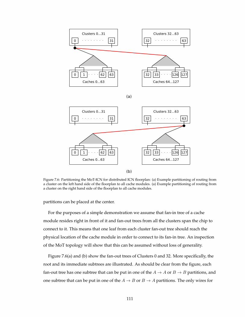
Clusters 0...31
0 31
Clusters 32...63
32 63
Caches 0...63
0 63
Caches 64...127
32 1271 62 33 126
Clusters 0...31
0 31
Clusters 32...63
32 63
Caches 0...63
0 63
Caches 64...127
32 1271 62 33 126
(a)
(b)
Figure 7.6: Partitioning the MoT-ICN for distributed ICN floorplan: (a) Example partitioning of routing froma cluster on the left hand side of the floorplan to all cache modules. (a) Example partitioning of routing froma cluster on the right hand side of the floorplan to all cache modules.
partitions can be placed at the center.
For the purposes of a simple demonstration we assume that fan-in tree of a cache
module resides right in front of it and fan-out trees from all the clusters span the chip to
connect to it. This means that one leaf from each cluster fan-out tree should reach the
physical location of the cache module in order to connect to its fan-in tree. An inspection
of the MoT topology will show that this can be assumed without loss of generality.
Figure 7.6(a) and (b) show the fan-out trees of Clusters 0 and 32. More specifically, the
root and its immediate subtrees are illustrated. As should be clear from the figure, each
fan-out tree has one subtree that can be put in one of the A→ A or B → B partitions, and
one subtree that can be put in one of the A→ B or B → A partitions. The only wires for
111

Clusters 0...31
0 31
Clusters 32...63
32 63
Caches 0...63
0 63
Caches 64...127
32 1271 62 33 126
Figure 7.7: Mapping of the partitioned MoT-ICN to the floorplan.
which the routing distance might increase are the ones that start at the tree roots and cross
from left to right or right to left (marked with red in the figure). This might incur
additional latencies for certain routing paths because of additional pipeline stages
required to keep the timing constraints. However this is a reasonable cost and be
alleviated via floorplan optimizations. Finally, Figure 7.7 shows how the connections can
be mapped on the floorplan.
7.3.1 Evaluation of Floorplans without DTM
We claimed that between the two floorplans we consider in this section, FP1 is superior to
FP2 in terms of thermal efficiency. Now, we verify this claim via simulation. We define
112

Figure 7.8: Temperature data from execution of the power-virus program on FP1, displayed as a thermal map.Brighter colors indicate hotter areas; highest and lowest temperatures are marked with yellow and blue boxes.
Figure 7.9: Temperature data from execution of the power-virus program on FP2, displayed as a thermal map.Brighter colors indicate hotter areas; highest and lowest temperatures are marked with yellow and blue boxes.
peak temperature as the highest temperature observed among the on-chip temperature
sensors. Assuming that our claim is correct, for a given program FP2 would yield a
113

higher peak temperature than FP1. If the temperature is a constraint, we would have to
bring the peak temperature of FP2 down by slowing its clock until the the temperature is
the same as for FP1. As a result, the program will take longer to finish in FP2. We
measure the overhead of a program on FP2, compared to FP1:
Overhead =RuntimeFP2 −RuntimeFP1
RuntimeFP1(7.1)
We repeat experiments for the two heatsink convection resistance values of 0.05K/W
and 0.1K/W . The initial experiment with an artificial power-virus program shows that
FP2 suffers from a 22% execution time overhead compared to FP1 (for both Rc values)
due to the reduced clock frequency required to meet the TDP. The program we simulated
in this experiment contains only arithmetic operations and no memory instructions.
Figures 7.8 and 7.9 display the temperature data from execution of the power-virus
program on FP1 and FP2 with Rc = 0.1K/W . This time the clock frequency was kept the
same, at 1.3GHz, in both experiments. Each figure shows maximum, minimum and
average temperatures. Brighter colors indicate hotter areas; highest and lowest
temperatures are marked with yellow and blue boxes. The data indicates that the highest
temperature in FP2 (370.95K = 97.80C) is approximately 5C higher than it is in FP1.
Moreover, the difference between the highest and the lowest temperatures is 18C whereas
it is almost half, 9.7C in FP1. The average temperatures are approximately the same in
FP1 and FP2. It is the more uniform distribution of temperature in FP1 that makes is more
thermally efficient.
A more realistic evaluation is shown in Fig. 7.10, where we repeat the same analysis on
our benchmark set. We choose a baseline clock frequency to accommodate the worst case
thermal limitations, as demonstrated by the most power consuming benchmark (Conv).
Limit temperature (Tlim) was set to 65C. The average cycle time overhead for
Rc = 0.05K/W is 13% and 16% for Rc = 0.1K/W (Tlim = 65K).
114

Rc = 0.05K/W Rc = 0.1K/W
0%
4%
8%
12%
16%
bfs-iibfs
bpropconv
fft mm
ult
msort
nw reduct
spmv
Ove
rhea
d
0%
4%
8%
12%
16%
bfs-iibfs
bpropconv
fft mm
ult
msort
nw reduct
spmv
Figure 7.10: Execution time overhead on FP2 compared to FP1.
7.4 DTM Background
DTM interacts with the system during runtime and usually operates at the architectural
level by utilizing tools such as dynamic voltage and frequency scaling (DVFS) and clock
and power gating (reviewed in Chapter 2). These tools can be applied globally or in a
distributed manner, where different parts of the chip are on different clock (and, if
available, voltage) domains. A comprehensive survey of various power and thermal
management techniques in uni-processors and multi-cores can be found in [KM08].
While distributed control is generally more beneficial, it also comes at a higher design
effort and implementation cost:
Clock domains: Separate clocks on a chip can be implemented via multiple PLL clock
generators and/or clock dividers. Alternatively, Truong, et al. [TCM+09] managed to
clock the 167 cores on their many-core chip independently using a ring oscillator and a set
of clock dividers per core.
Voltage Domains: One of the strategies for multiple on-chip voltage domains is voltage
islands [LZB+02]. Voltage islands are silicon areas in a chip that are fed by a common
supply source through the same package pin. The advantage of voltage islands is
separate islands can be managed independently according to their activation pattern. For
the routing to be feasible, the transistors in the same voltage group should physically be
placed together. Another strategy is to distribute two or more power networks to the chip
in parallel [TCM+09]. In this scenario, design is considerably simpler but the voltage
choices are limited to two. The two voltages can still be modified dynamically at the
115
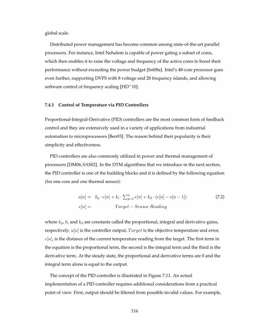
global scale.
Distributed power management has become common among state-of-the-art parallel
processors. For instance, Intel Nehalem is capable of power gating a subset of cores,
which then enables it to raise the voltage and frequency of the active cores to boost their
performance without exceeding the power budget [Int08a]. Intel’s 48-core processor goes
even further, supporting DVFS with 8 voltage and 28 frequency islands, and allowing
software control of frequency scaling [HD+10].
7.4.1 Control of Temperature via PID Controllers
Proportional-Integral-Derivative (PID) controllers are the most common form of feedback
control and they are extensively used in a variety of applications from industrial
automation to microprocessors [Ben93]. The reason behind their popularity is their
simplicity and effectiveness.
PID controllers are also commonly utilized in power and thermal management of
processors [DM06, SAS02]. In the DTM algorithms that we introduce in the next section,
the PID controller is one of the building blocks and it is defined by the following equation
(for one core and one thermal sensor):
u[n] = kp · e[n] + ki ·∑n
y=1 e[n] + kd · (e[n]− e[n− 1]) (7.2)
e[n] = Target− Sensor Reading
where kp, ki and kd are constants called the proportional, integral and derivative gains,
respectively. u[n] is the controller output, Target is the objective temperature and error,
e[n], is the distance of the current temperature reading from the target. The first term in
the equation is the proportional term, the second is the integral term and the third is the
derivative term. At the steady state, the proportional and derivative terms are 0 and the
integral term alone is equal to the output.
The concept of the PID controller is illustrated in Figure 7.11. An actual
implementation of a PID controller requires additional considerations from a practical
point of view. First, output should be filtered from possible invalid values. For example,
116

Core
∑
-
+Target
PID Calculation
Sensor
reading
Controller
output (u[n])
Frequency
voltage
Workload
Error (e[n])
Figure 7.11: PID controller for one core or cluster and one thermal sensor.
at times the output might turn to very small negative values due to quantization errors,
which should not be allowed. Second, the integral term should be protected against a
phenomenon called integral windup. This happens in cases where the the power
dissipation is so low that the core works at the maximum frequency but the temperature
reading is still under the target value (i.e., error is non-zero). The error will continuously
accumulate on the integral term, causing it to increase arbitrarily. Eventually, if power
dissipation does increase and temperature overshoots the target, it will take the integral
output a long time to “unwind”, i.e., return to a reading that is within the meaningful
input range. Integral windup is can be avoided by limiting the range of the integral term.
The code given next represents our implementation of the PID controller in XMTSim.
// k_p , k_i , and k_d are constant parameters .// t a r g e t i s the t a r g e t temperature .double c o n t r o l l e r ( double sensor_reading ) {
double l a s t _ e r r o r = e r r o r ;double e r r o r = t a r g e t − sensor_reading ;// Ca l cu l a te the propor t iona l term .double propor t iona l = k_p ∗ e r r o r ;// Ca l cu l a te the i n t e g r a l term .double i n t e g r a l += k_i ∗ e r r o r ;// Prevent the i n t e g r a l windup .i f ( i n t e g r a l > i n t e g r a l _ f r e e z e ) i n t e g r a l = i n t e g r a l _ f r e e z e ;i f ( i n t e g r a l < 0) i n t e g r a l = 0 ;// Ca l cu l a te the d e r i v a t i v e term .double d e r i v a t i v e = k_d ∗ ( e r r o r − l a s t E r r o r ) ;double c o n t r o l l e r _ o u t p u t = propor t iona l + i n t e g r a l + d e r i v a t i v e ;// C o n t r o l l e r output should not take an i n v a l i d value even i f i t i s// n e g l i g i b l e .i f ( c o n t r o l l e r _ o u t p u t < lowerBound )
c o n t r o l l e r _ o u t p u t = lowerBound ;i f ( c o n t r o l l e r _ o u t p u t > upperBound )
c o n t r o l l e r _ o u t p u t = upperBound ;re turn c o n t r o l l e r _ o u t p u t ;
}
117

For complex systems, values of the parameters, kp, ki, and kd are determined through
well established procedures. In our case, simple experimentation was sufficient to derive
parameters values for a fast converging control mechanism.
Other controllers (ex., model predictive control [BCTB11]) are also proposed in the
literature . These controllers can yield better convergence times compared to PID
controllers, however this was not an immediate issue for our experiments, therefore we
leave incorporating these controllers as future work.
7.5 DTM Algorithms and Evaluation
In this section, we evaluate a set of DTM techniques that can potentially improve the
performance of the XMT1024 processor. Our main objective is obtaining the shortest
execution time for a benchmark without exceeding a predetermined temperature limit.
Note that energy efficiency is not within the scope of this objective.
In our experiments, we evaluated the following DTM techniques that are motivated by
the previous work on single and multi-cores [KM08]. We adapted these techniques to our
many-core platform.
GDVFS (Global DVFS): All clusters, caches and the ICN are controlled by the same
controller. The input of the controller is the maximum temperature among the clusters
and the output is the global voltage and frequency values. Global DVFS is the simplest
DTM technique in terms of physical implementation therefore any other technique
should perform better in order to justify its incorporation.
CG-DDVFS (Coarse-Grain Distributed DVFS): In addition to the global controller for
clusters, the ICN is controlled by a dedicated controller. The input of this controller is the
maximum temperature measured over the ICN area. Some many-cores, such as GTX280,
already have separate clock domains for the computation elements and the
interconnection network, leading us to conclude that the implementation cost of this
technique is acceptable.
FG-DDVFS (Fine-Grain Distributed DVFS): Each cluster has a separate voltage island
and is controlled by an independent DVFS controller. The input of a controller is the
118

Table 7.2: The baseline clock frequencies
Rc = 0.05K/W Rc = 0.1K/WFP1 69% 34%FP2 60% 29%
temperature of the cluster and the output is the voltage and frequency values. The cache
frequency is equal to the average frequency of the clusters. The ICN is controlled by a
dedicated controller as in CG-DDVFS. The implementation of this technique may be
prohibitively expensive on large systems due to the number of voltage islands.
LP-DDVFS (Distributed DVFS for Low-Parallelism): This technique is only relevant for
the benchmarks that have significant portions of parallel execution during which the
number of threads is less than the number of TCUs. In XMT, threads are spread out to as
many clusters as possible in order to reduce resource contention. However, this approach
prevents us from placing the unused TCUs in the off state (i.e. voltage gating) and the
wasted static power cannot be used towards increasing the dynamic power envelope.
LP-DDVFS groups the threads into a minimal number of clusters. The unutilized clusters
are then placed in the off state, and the saved power is utilized by increasing the clock
frequency of the active clusters. The implementation cost of this technique is proportional
to the complexity of thread scheduling, which is very low on XMT.
7.5.1 Analysis of DTM Results
To form a baseline for assessing the efficiency of the DTM techniques listed above, we
simulated all the benchmarks on an XMT configuration with no thermal management.
We assume that such a system is optimized to run at the fastest clock frequency that is
thermally feasible for the worst case (i.e. the most active, most power consuming)
benchmark, which was shown to be Conv in Section 7.2. Table 7.2 lists these clock
frequencies as a percentage of the maximum cluster clock frequency. The table contains
one entry per convection resistance and floorplan combination, as they determine the
thermal response of the chip. The entry for FP2 and Rc = 0.1K/W requires the lowest
clock frequency therefore it constitutes the strictest thermal constraint. Similarly, the entry
for FP1 and Rc = 0.05K/W constitutes the least restrictive thermal constraint.
In Figures 7.12 and 7.13, we list the benchmark speedups when simulated with the
119

various DTM techniques. The speedup of a benchmark is calculated using the following
formula:
S =ExecbaseExecdtm
(7.3)
where Execbase and Execdtm are the execution times on the baseline system and with
thermal management, respectively. The benchmarks are divided into graphs according to
their overall activity levels, where the top row is for the high activity benchmarks and
bottom row is for the low activity benchmarks. Within each row there are four subgraphs,
each of which corresponds to one of the four entries in Table 7.2.
As a general trend, the benchmarks that benefit the most from the DTM techniques are
benchmarks with low cluster activity factors, namely Bfs-I, Bfs-II, Bprop, Nw and Msort
(note the scale difference between the y axes of the two rows of Figures 7.12 and 7.13).
The highest speedups are observed for Bfs-II with the DTM techniques that incorporate a
dedicated ICN controller, CG-DDVFS and FG-DDVFS (up to 46% better speedup than
GDVFS). There are two underlying reasons for this behavior. First, Bfs-II is mainly bound
by memory latency, hence it benefits greatly from the increased ICN frequency. Moreover,
it has very low overall activity and runs at the maximum clock speed without even
nearing the limit temperature. On the other extreme, Conv has the highest cluster activity
and was used as the worst case in determining the feasible baseline clock frequency, and
therefore shows the least improvement in most experiments.
We also observe that as the thermal constraints become stricter, the average speedup
increases and the variation between speedups widens. This trend is clearly visible when
comparing the low activity benchmarks with the two Rc values. In order to clarify the
cause for this phenomenon, recall that the benchmark runtimes with DTM are compared
against the runtimes with the baseline clock frequency, which is optimized for the worst
case. The no-DTM case penalizes the lowest activity benchmarks unnecessarily, and this
penalty increases further as the thermal constraints tighten (as can be seen from
Table 7.2). On the other hand, if DTM is present, the overhead of the low activity
benchmarks will not change as significantly with tighter thermal constraints.
In the remainder of this section we will concentrate on the performance of individual
DTM techniques and conclude by revisiting the effect of floorplan on performance.
120

High Activity Benchmarks
Rc=0.05K/W Rc=0.1K/W
1.0
1.1
1.2
1.3
1.4
1.5
1.6
spmv
reduct
convm
mult
fft
Spe
edup
GDVFSCG−DDVFSFG−DDVFS
1.0
1.1
1.2
1.3
1.4
1.5
1.6
spmvreduct
convmmult
fft
Low Activity Benchmarks
Rc=0.05K/W Rc=0.1K/W
1.0
1.5
2.0
2.5
3.0
3.5
4.0
4.5
bfs−ibfs−ii
bprop
nw msort
Spe
edup
1.0
1.5
2.0
2.5
3.0
3.5
4.0
4.5
bfs−ibfs−ii
bprop
nw msort
Figure 7.12: Benchmark speedups on FP1 with DTM. Each graph shows results with a different convectionresistance (Rc) and floorplan combination. The benchmarks are grouped into high (top graphs) and low(bottom graphs) cluster activity. Note that the two groups have different y-axis ranges.
121

High Activity Benchmarks
Rc=0.05K/W Rc=0.1K/W
1.0
1.1
1.2
1.3
1.4
1.5
1.6
spmvreduct
convmmult
fft
Spee
dup
1.0
1.1
1.2
1.3
1.4
1.5
1.6
spmvreduct
convmmult
fft
Low Activity Benchmarks
Rc=0.05K/W Rc=0.1K/W
1.0
1.5
2.0
2.5
3.0
3.5
4.0
4.5
bfs−ibfs−ii
bprop
nw msort
Spe
edup
GDVFSCG−DDVFSFG−DDVFS
1.0
1.5
2.0
2.5
3.0
3.5
4.0
4.5
bfs−ibfs−ii
bprop
nw msort
Figure 7.13: Benchmark speedups on FP2 with DTM. Each graph shows results with a different convectionresistance (Rc) and floorplan combination. The benchmarks are grouped into high (top graphs) and low(bottom graphs) cluster activity. Note that the two groups have different y-axis ranges.
122

7.5.2 CG-DDVFS
The CG-DDVFS technique is only effective when the thermal constraints are not very
tight (i.e. Rc = 0.05K/W ) and generates good results on a subset of the low activity
benchmarks: Bfs-I, Bfs-II, Nw and Msort, which run below the thermal limit for the
majority of their execution time. This allows them to maximize the ICN clock frequency,
providing speedups of 17% (Msort), 25% (Bfs-II), 30% (Nw) and 46% (Bfs-II) over GDVFS
on both floorplans. With Rc = 0.1K/W , all benchmarks but Bfs-II reach the thermal limit
temperature. In this case, the gains are not significant except for a few noticeable cases:
Bfs-I, (14% over GDVFS) and Nw (10% over GDVFS). Bfs-II’s gain stays at 46% as it is still
under the thermal limit. A common property of these benchmarks, aside from the low
overall activity factors, is how the cluster and ICN activities compare: their ICN activity is
higher than the cluster activity, as opposed to the rest of the benchmarks, for which it is
the opposite. At the source of this observation lies the fact that higher ICN to cluster
activity ratio is common in programs with irregular memory accesses and low
computation. An exception is the Bprop benchmark, for which the bottleneck is queuing
on data. For the remainder of the benchmarks, we observed that CG-DDVFS may hurt
performance by up to 12% with respect to GDVFS.
Insight: For a system with a central interconnection component such as XMT, workloads
that are characterized by scattered irregular memory accesses usually benefit more from a
dedicated interconnect thermal monitoring and controller. This information can influence
the choice of DTM for a system that targets such workloads. We also saw that dedicated
ICN control based on thermal input can hurt performance for regular parallel benchmarks
with high computation ratios. This observation gives a good decision mechanism to a
general-purpose system for picking up the instances when CG-DDVFS should be applied.
We incorporated dynamic activity monitoring into the control algorithm of CG-DDVFS,
and fall back to GDVFS whenever the ICN activity is lower than the cluster activity. The
speedup values in Figures 7.12 and 7.13 reflect this addition to CG-DDVFS.
123

7.5.3 FG-DDVFS
As indicated in Section 7.2, the activity of clusters does not vary significantly over the
chip area at a given time, when considering a single task and time window that is
comparable to the duration for a significant change in temperature to occur. Therefore,
the only benefit that FG-DDVFS can provide to a single tasking system is a result of the
temperature difference between the middle of the die, where the clusters are hotter, and
the edges. A distributed DTM technique requires fine granularity of hardware control for
voltage and frequency, which is costly in terms of added hardware complexity.
Consequently, the associated benefits of such a scheme need to justify the added
overhead. As can be seen in Figures 7.12 and 7.13, the added value of FG-DDVFS is more
apparent for higher activity benchmarks such as Spmv, Reduct, Conv and FFT. For these
benchmarks the combined effect of ICN and distributed cluster scaling provides a
speedup of up to 22% (Reduct in FP2 and Rc = 0.05K/W ) over GDVFS.
Insight: Individual temperature monitoring and control for computing clusters may be
worthwhile even in a single-tasking system with fairly uniform workload distribution.
The gains are noteworthy for regular parallel programs with high amounts of
computation. Conversely, the overall performance of FG-DDVFS on the low activity
benchmarks may not justify its added cost for some systems.
An interesting insight to the operation of FG-DDVFS is as follows. Typically, with a
global cluster controller, the edges of the chip will be cooler than the thermal limit
temperature. A per cluster controller mechanism will try to pick up this thermal slack by
increasing clock frequency at the edge clusters. However, as the temperature of the edge
clusters rise, so does the temperature of the center clusters and the controllers will
respond by converging at lower clock frequencies.
7.5.4 LP-DDVFS
The LP-DDVFS technique is relevant only for a small subset of the simulated benchmarks
- those with low parallelism. The only two benchmarks to which LP-DDVFS would apply
are Mmult and Nw, both of which were classified as low-p type (see Table 7.1). The third
low parallelism benchmark, Bfs-II, would not benefit from this technique for the
124

simulated parameters. This is because Bfs-II already operates at the maximum clock
frequency, meaning that the reduced power consumption resulting from voltage gating
the clusters in the off state cannot be translated into performance gain. The LP-DDVFS
techniques provides performance gains of 10%-12% over GDVFS for the low parallelism
benchmarks.
Insight: In a clustered architecture such as XMT, threads of programs with low levels of
parallelism can be assigned to clusters in two ways with conflicting benefits. On the one
hand, distributing threads between clusters increases performance due to reduced
contention on shared resources. On the other hand, when threads are grouped, off clusters
can be voltage gated, allowing us to route the saved static power towards increasing the
clock frequency of the active ones. The optimal choice is benchmark dependent. For
example, a benchmark such as Bfs-II does not benefit from the latter. This fact
demonstrates the need for dynamic control of assignment of threads to clusters.
7.5.5 Effect of floorplan
We revisit Figure 7.10, this time including the effect of thermal management. Figure 7.14
compares the runtimes of the benchmarks on the two floorplans with DTM. As expected,
the low-activity benchmarks show the least difference between the two floorplans since
they operate at near maximum clock speeds (except for Bfs-II when Rc = 0.05K/W ,
which is bound by the ICN activity). For the rest of the benchmarks, application of DTM
seems to lessen the differences between the floorplans.
7.6 Future Work
XMTSim opens up a range of possibilities for evaluating power and thermal management
algorithms in the many-core context. In this chapter, we evaluated thermal management
algorithms in a single-tasked environment. Some other possibilities are as follows.
New metrics for management. Total energy consumption and power envelope are
some of the other relevant metrics that can be considered for dynamic management. Total
energy is especially important for mobile devices, which are limited by battery life, and
125

Rc = 0.05K/W
0% 2% 4% 6% 8%
10% 12% 14%
bfs−ii
bfs−ibprop
convfft m
mult
msort
nw reduct
spmv
Ove
rhea
d
GDVFSCG−DDVFSFG−DDVFS
Rc = 0.1K/W
−5%
0%
5%
10%
15%
20%
bfs−ii
bfs−ibprop
convfft m
mult
msort
nw reduct
spmv
Ove
rhea
d
Figure 7.14: Execution time overheads on FP2 compared to FP1 under DTM.
126

data centers, where the cost of energy adds up to significant amounts. Power envelope,
similar to thermal envelope, is related to the feasibility of the system. In this case, the
power plan for the processor may enforce a specific power envelope. Also, in large
systems such as server farms, it might be desirable to modify the the power density for
certain groups of processors dynamically.
Dynamic thermal/power management in a multi-tasking environment. Consider an
XMT system with multiple master TCUs. Such a system would be capable of running
multiple parallel programs concurrently, each program assigned to one master TCU. Total
number of parallel TCUs would be shared among the master TCUs statically or
dynamically. In this environment, dynamic management becomes an optimization
problem with many variables. Given a set of parallel tasks, first the algorithm should
choose the tasks that should be run at the same time. Then, it should decide an
appropriate power/performance point for each task. The parameters for fixing the
power/performance point are the number of parallel TCUs to be allocated for the task
and frequency/voltage values of the TCUs.
7.7 Related Work
A vast amount of literature is dedicated to the thermal management of systems with dual,
quad or 8 core processors (for a summary, see book by Kaxiras and Martonosi [KM08]).
However, the interest in the thermal management of more than tens of cores on a chip is
relatively recent. A factor that stands in the way of extended research in this area is the
scarcity of widely accepted power/thermal enabled simulators and also the lack of
consensus on the programming model and architecture of such processors. Many of the
current research papers on the thermal management of many-cores start with less than
100 cores. They assume a pool of uncorrelated serial benchmarks as their workload and
capitalize on the variance in the execution profiles of these benchmarks. Some examples
are [LZWQ10, KRU09, GMQ10]. However, it is simply not realistic to assume that an OS
will provide a sufficient number of independent tasks to occupy all the cores in a
general-purpose many-core with 1000s of cores. It is evident that single-task parallelism
should be included in the formulation of many-core thermal management. Even though
127

it focuses on power rather than thermal management and considers up to only 128 cores,
the study by Ma, et al. [MLCW11] should be mentioned as they simulate a set of parallel
benchmarks and in this respect they are closer to our vision.
128

Chapter 8
Conclusion
In this thesis we investigated the power consumption and the thermal properties of the
Explicit Multi-Threading (XMT) architecture from a high-level perspective. XMT is a
highly-scalable on-chip many-core platform for improving single-task parallelism. One of
the fundamental objectives of XMT is ease-of-programming and our study aims to
advance the high impact message that it is possible to build a highly scalable general-purpose
many-core computer that is easy to program, excels on performance and is competitive on power.
We hope that our findings will be a trailblazer for future commercial products. More
concretely, the contributions of this thesis can be summarized as follows:
• We implemented XMTSim, a highly-configurable cycle-accurate simulator of the
XMT architecture, complete with power estimation and dynamic power/thermal
management features. XMTSim has been vital in exploring the design space for the
XMT computer architecture, as well as establishing the ease-of-programming and
competitive performance claims of the XMT project. Furthermore, the capabilities
XMTSim extend beyond the scope of the XMT vision. It can be used to explore a
much greater design space of shared memory many-cores by a range of researchers
such as algorithm developers and system architects.
• We used XMTSim to compare the performance of an envisioned 1024-TCU XMT
processor (XMT1024) with an NVIDIA GTX280 many-core GPU. We enabled a
meaningful comparison by establishing the XMT configuration that is silicon
area-equivalent to GTX280. Results from the ASIC tape-out of a 64-TCU XMT ASIC
prototype, to which we contributed at the synthesis stage, was partly used in
derivation of the XMT configuration. Simulations show that the XMT1024 provides
2.05x to 8.10 speedups over GTX280 on irregular parallel programs, and slowdowns
of 0.23x to 0.74x on regular programs. In view of these results, XMT is
well-positioned for the mainstream general-purpose platform of the future,
129

especially when coupled with a GPU.
• We extended the XMT versus GPU comparison by adding a power constraint,
which is crucial for supporting the performance advantage claims of XMT. A
complete comparison of XMT1024 and GTX280 should essentially show that, not
only they are area-equivalent but also XMT1024 does not require higher power
envelope than GTX280 for achieving the above speedups. Our initial experiments
suggested this is indeed the case, however power estimation of a simulated
processor is subject to unexpected errors. Therefore we repeated the experiments
assuming that our initial power model was imperfect in various aspects. We show
that for the best case scenario XMT1024 over-performs GTX280 by an average of
8.8x on irregular benchmarks and 6.4x overall. Speedups are only reduced by an
average of 20% for the average-case scenario and approximately halved for the
worst-case. Even for the worst case, XMT is an viable option as a general-purpose
processor given its ease-of-programming.
• We explored to what extent various dynamic thermal management (DTM)
algorithms could improve the performance of the XMT1024 processor. DTM is well
studied in the context of multi-cores up to 10s of cores but we are among the first to
evaluate it for a many-core processor with 1000+ cores. We observed that in the
XMT1024 processor with fine-grained parallel workloads, the dominant source of
thermal imbalance is often between the cores and the interconnection network. For
instance, a DTM technique that exploits this imbalance by individually managing
the interconnect can perform up to 46% better than the global DTM for irregular
parallel benchmarks. We provided several other high-level insights on the effect of
individually managing the interconnect and the computing clusters.
The material in Chapters 4 and 5 has appeared in [KTC+11] and [CKTV10] as peer
reviewed publications. The work presented in Chapters 6 and 7 is currently under
review for publication.
130

Appendix A
Basics of Digital CMOS Logic
The majority of the modern commercial processors are designed with Metal-Oxide
Semiconductor (MOS) transistors. Complementary-MOS (CMOS) is also the most
common circuit design methodology used in constructing logic gates with MOS
transistors. In this section, we give a brief background on power dissipation and speed of
CMOS circuits.
A.1 The MOSFET
Metal-Oxide Semiconductor Field Effect Transistors (MOSFETs, or MOS transistors) are
the building blocks of CMOS circuits. For the purposes of digital circuits, a MOSFET is
expected to act as an ideal switch. The vertical cross section of a MOSFET as well as the
circuit symbols for n and p types (explained next) are given in Figure A.1. The gate is the
control terminal and when an ideal transistor is on, it forms a low-resistance conductive
path (i.e., channel) between the source and the drain terminals1. The connection does not
exist when the transistor is off. Two types of MOS transistors are used in CMOS circuits:
(i) an n-channel MOS (nMOS) transistor is on when high voltage is applied to its gate
(VGS = (VG − VS) > vth) and, (ii) a p-channel MOS (pMOS) transistor is on at low voltage
input (VGS = (VG − VS) < −vth). vth is the transistor threshold voltage and it is a positive
number. The value of VGS − vth for nMOS or −VGS − vth for pMOS is called the gate
overdrive. Higher gate overdrive values result in faster and more ideal switch behavior.
A.2 A Simple CMOS Logic Gate: The Inverter
Figure A.2 shows a CMOS inverter, which is the simplest of CMOS logic gates. We use it
to demonstrate the working principles of CMOS gates.
1The fourth terminal, body (or substrate) connection, is not crucial for the purposes of this introduction.
131

Source
Gate
Drain
Channel
Body
Gate-oxideVG
VS
VD
VB ISDVG
VD
VS
VB IDS
(a) (b)
Figure A.1: (a) Vertical cross-section of a MOSFET along its channel. (b) Circuit symbols of pMOS and nMOStransistors.
Supply Voltage -- Vdd
Ground voltage -- 0V
Load
(modeled as capacitance)
Transistor current paths
for ON state
Transistor gate
terminals
Input Output
M1
M2
Figure A.2: The CMOS inverter.
The inverter consists of two transistors: the nMOS (M2 in the figure) is on when gate
voltage is high and the pMOS (M1 in the figure) is on when its gate voltage is low. Since
binary logic assumes only two voltage levels - low and high - it is clear that only one
transistor can be on at a given time. Ideally, the one that is off acts as an open circuit and,
at any given time, the output is connected to either Vdd (when input is low and M1 is on)
or to ground (when input is high and M2 is on). For the transistor that is on, the value of
|VG − VS | is equal to Vdd, therefore gate overdrive is Vdd − vth.
Other logic functions can be obtained by replacing the pMOS and nMOS transistors of
the inverter with more complex pMOS and nMOS transistor networks, so-called pull-up
and pull-down networks. The overall circuit still operates according to the same principle:
only one of the pull-up and pull-down networks can have a conductive path at any given
time.
Average time that it takes for a CMOS gate to switch between states (td) depends on the
drive strength of the transistors in it. The drive strength is a function of the supply
132

voltage and the gate overdrive [SN90]:
td ∝Vdd
(Vdd − vth)a(A.1)
The constant, a is a technology dependent parameter between 1 and 2 with a typical
value close to 2, therefore gate delay is assumed to be proportional to voltage. The
equation ceases to hold for very high values of Vdd due to the velocity saturation
phenomenon, which causes the effective value of a to drop down to 1.
Switching time, td, is also proportional to the gate load capacitance. The output of a
CMOS gate is essentially connected to the inputs of other gates. The total capacitance at
the output node, which is the sum of the parasitic capacitances of all connected gates, is
called the load capacitance. When the logic state of the gate changes, the output
capacitance charges (or discharges) to the new voltage. The switching speed of a gate, td,
depends on its output (or load) capacitance and its drive strength, a function of the supply
voltage and gate overdrive [SN90].
A.3 Dynamic Power
Charge/discharge of capacitive loads (switching power) and short circuit currents are the
two mechanisms that cause the dynamic power of CMOS circuits. In modern circuits,
short circuit currents are usually negligible and switching power is dominant.
Figure A.3 illustrates the series of events that lead to the dynamic power dissipation in
an inverter gate. Low voltage state (ideally 0V) is assumed to correspond to binary value
0 and high voltage (ideally Vdd) to binary value 1. At the initial and final states
(Figs. A.3(a) and A.3(d)), no dynamic power is spent. Short circuit current is observed
only during the brief time that both gates are active, as shown in Figs. A.3(b). Switching
current exists during the entire transition. In the following subsections, we explain the
switching power and short circuit power in detail.
133

ON
ON
OFF
Isc
Input=
high to low
Input=low
VddVdd
Output=high
(b)(a)
Load
discharged
Isw
OFF
ON
Input=low
Vdd
Output=
low to high
(c)
Isw
OFF
ON
Input=low
Vdd
Output=high
(d)
Load
charged
ON
Figure A.3: Dynamic currents during the logic state transition of an inverter from 0 to 1: (a) initial state, nodynamic power is spent, (b) short circuit (Isc) and switching current (Isw) observed during transition, (c) Iswcontinues until the transition is completed, (d) new state.
A.3.1 Switching Power
In CMOS logic gates, binary states are represented with high and low voltage levels and
switching from one level to another results in charging or discharging of the load
capacitance at the output of the gate. In an aggressively optimized logic circuit, the
switching power is proportional to the amount of work performed. Unlike the other
power components, it cannot be brought down to a negligible value via conservative
design constraints or advanced technologies.
The overall switching power of a logic circuit consisting of many gates, Psw, is
described as follows [Rab96]:
134

PSW ∝ CLVdd2fα (A.2)
CL is the average load capacitance of the gates, Vdd is the supply voltage, f is the clock
frequency and α is the average switching probability of the logic gate output nodes.
A.3.2 Short Circuit Power
During the logic state switch of a gate, for a brief moment the input voltage sweeps
intermediate values. Intermediate levels at the input of a gate cause both the pull-up and
pull-down circuits (M1 and M2 for the inverter in Figure A.2) to conduct for a short
period of time as illustrated in Figure A.3(b). The resulting power consumption is
described by the following equation [Vee84].
PSC ∝W
L(Vdd − 2 · Vth)
3τf (A.3)
W and L are the channel width and length in a CMOS transistor, Vth is the threshold
voltage and τ is the average input rise and fall time. As mentioned earlier, short circuit
power is negligible in comparison to the switching power.
A.4 Leakage Power
An ideal MOSFET switch is expected not to conduct any current between its drain and
source terminals in the off state. Also, the gate of the transistor is intended to act as an
ideal insulator at all times. In reality, these assumptions do not hold and in addition to the
active power, the transistor consumes power due to various leakage currents. The
amount of leakage has become significant in the deep sub-micron era. Below is a list of
the leakage currents that we discuss in this section and Figure A.4 illustrates these
currents on a vertical cross-section of a MOS transistor.
I1 – Subthreshold leakage
I2 – Gate oxide tunneling leakage
I3 – Gate induced drain leakage (GIDL)
135

Source Drain
Gate
I1
I2
I3
I4
Figure A.4: Overview of leakage currents in a MOS transistor.
OFF
ON
ON
OFF
Isub
Igate
Input=high
Input=low
Igate
Vdd Vdd
Output=low Output=high
(a) (b)
Isub
Figure A.5: Subthreshold (Isub) and gate (Igate) leakage currents during inactive states of a CMOS inverter (a)transistor output is logic-low (b) transistor output is logic-high.
I4 – Junction leakage
Among the currents listed above, subthreshold leakage has historically been the dominant
one. Gate-oxide tunneling has gained importance with the scaling of transistor gate
oxides. Junction leakage along with GIDL becomes significant in the presence of body
biasing techniques that might reduce other types of leakage (discussed in Section 2.3.1).
Figure A.5 demonstrates the subthreshold and gate leakage currents on logic-high and
logic-low states of an inverter gate. As the figure shows, subthreshold leakage causes a
constant current path from supply voltage to ground and gate leakage induces current
through the gate of the off transistor.
A.4.1 Subthreshold Leakage
Subthreshold leakage power (Psub) typically dominates the off-state power in modern
devices. It is caused by the inability of the transistor to switch off the path between its
136

VGS
log(IDS)
Vth
Ideal threshold
cut-off
Subthreshold
current
Figure A.6: Drain current versus gate voltage in an nMOS transistor with constant VDS . The inverse of thesubthreshold slope has typical values ranging from 80 to 120 mV per decade.
source and drain terminals and as we will show, it is strongly related to the threshold
voltage. Figure A.6 depicts the drain to source current (IDS) as a function of gate voltage
(VGS). The section where VGS is lower than the threshold voltage plots the subthreshold
leakage current (Isub).
Psub and Isub are modeled via the following equations [ZPS+03].
Psub = Isub · Vdd (A.4)
Isub = µ0 · Cox ·W
L· eb(Vdd−Vdd0) · v2t · (1− e
−Vddvt ) · e
−|vth|−Voffn·vt (A.5)
According to Equation (A.4) leakage power is a function of several parameters, most
importantly the supply voltage (Vdd), temperature, which is included in the thermal
voltage (vt = kT/q, where k is the Boltzmann constant and q is the electron charge) and
the MOS threshold voltage (vth). The parameters vt and vth are both functions of
temperature. We will further elaborate on this equation next.
Literature contains a vast number of research papers written on the subject of
subthreshold leakage (and leakage in general) which represent its dependence on the
parameters listed above in various ways (ex., [ZPS+03, BS00]). This is a result of the the
inevitable complexity of the model and the hidden interdependencies between the
parameters of Equation (A.4). The changes brought by advancing technologies and
137

miniaturization of transistors further exacerbates the complexity. For example, the charge
mobility, µ0, is a function of temperature however, some papers list it as a constant, which
is an adequate approximation in some cases. For our purposes, we will reduct
Equation (A.4) to a simpler form which is sufficient to explain trends in computer design.
The term Cox · WL contains the effect of the the geometry of the transistor (gate oxide
thickness, transistor channel width and length) and can be interpreted as a technology
node dependent constant, TECH . µ0, as mentioned earlier, is cited as a constant or as
proportional to a power of the temperature (T−1.5in [GST07], depending on the context.
Combined with v2t , we will express this term as a polynomial function of temperature,
ρ(T ). The term (1− e−Vddvt ) is approximately 1 for the values of V dd ([0.9V, 1.2V ]) and T
([27C, 110C]) we consider so it will be omitted. The effective threshold voltage of the
transistor, vth, is a function of temperature and expressed as
vth = vth0 − c · (T − T0) (A.6)
where vth0 is the base threshold voltage, c is a constant and T0 is the initial temperature. b,
Vdd0, n, and Voff are technology dependent constants (Voff might depend on temperature
but taken as a constant here). Also, recall that vt ∝ T . Finally, all terms of Equation (A.4)
are arranged into the following relation (exp(.) signifies an exponential dependency in the
form of exp(x) = ekx, where k is a constant).
Psub ∝ TECH · ρ(T ) · V · exp(V ) · exp(−Vth0
T) · exp(− 1
T) (A.7)
It should be noted that, while the simpler equation explains the behavior of
subthreshold leakage for past and recent technologies, it might not hold below the 32nm
technology node with the addition of factors such as short channel effects. Also, so far we
have only focused on a single transistor. Further steps are required to carry the analysis to
the chip scale since the coefficients of the equation vary for different transistors on the
chip. Nevertheless, the observations we listed for Equation (A.7) hold at the macro level,
which is the purpose of this discussion.
138

A.4.2 Leakage due to Gate Oxide Scaling
Gate oxide thickness (see Figure A.1), is a technology parameter that has been
aggressively scaled to control the threshold voltage and improve switching performance.
However, scaling of gate oxide comes at the cost of triggering additional leakage
mechanisms that have not been of concern before. These mechanisms are gate oxide
tunneling leakage and gate induced drain leakage (GIDL). Explicit equations for the
associated currents are difficult to obtain hence we only give the intuition on the factors
that affect these currents.
Gate oxide tunneling leakage is a result of quantum tunneling, where electrical charges
tunnel through an insulator (barrier). This phenomenon is especially detectable for thin
barriers (i.e., gate oxide) and high potential energy differences (i.e., voltage), therefore it is
very sensitive to gate oxide thickness (tox) and supply voltage. It has a weak dependency
on temperature. At 70nm, tox = 1.2nm (which is a typical value), Vdd = 0.9 and room
temperature (300K), gate leakage is in the order of 40nA/µm [ZPS+03].
GIDL is caused by the tunneling effect at the overlap of gate and drain and it can
become a limiting factor for the adaptive body biasing technique which is mentioned in
Section 2.3.1.
A.4.2.1 Junction Leakage
Junction leakage is observed at the drain/body and source/body junctions. There can be
multiple mechanisms contributing to junction leakage such as tunneling effects or reverse
bias junction leakage. Similar to GIDL, the effect of junction leakage becomes relevant
especially if reverse body biasing technique is used [MFMB02, KNB+99].
139

Appendix B
Extended XMTSim Documentation
This appendix contains detailed documentation of XMTSim, including installation
instruction, a command line usage manual, software architecture overview, programming
API and coding examples for creating new actors, activity monitors, etc.
B.1 General Information and Installation
XMTSim is typically used with the XMTC compiler which is a separate download
package. It can be used standalone in cases that the user directly writes XMT assembly
code.
To use XMTSim, you must:
• Download and install the XMTC compiler (typically).
• Download and install XMT memory tools (optional).
• Build/install XMTSim.
The XMT toolchain can be found at
http:
//www.umiacs.umd.edu/users/vishkin/XMT/index.shtml#sw-release
and also on Sourceforge
http://sourceforge.net/projects/xmtc/
B.1.1 Dependencies and install
Pre-compiled binary distribution consists of a Java jar file and a bash script file. Due to
platform independent nature of Java, this distribution is platform independent as well.
140

The cygwin/linux dependent bash script is distributed for convenience and is not an
absolute requirement. In future distributions, simulator may include platform dependent
components.
System requirements:
• You must have Sun Java 6 (JRE - Java Runtime Environment) or higher on your
system. Java executable must be on your PATH, i.e. when you type "java -version"
on command line you should see the correct version of Java. XMTSim might work
with other implementations of Java that are equivalents of the Sun Java 6 (or higher)
however it is only tested with the Sun version of Java. Note that the XMTC
compiler and memory tools come with their own set up system requirements that
are independent of the simulator.
• In order to use the script provided in the package, you must have bash installed on
your system. XMTSim can directly be run via the "java -jar" command. Read the
xmtsim script if you would like to use the simulator in such a way.
Follow these steps to install XMTSim:
a) Create a new directory of your choice and place the contents of this package in the
directory. Example: /xmtsim
b) Make sure java is on the PATH:
> java -version
The commands should display the correct java version.
c) Add the new directory to the PATH. Example (bash):
> export PATH=~/xmtsim:$PATH
d) Test your installation:
> xmtsim -version
> xmtsim -check
Type “xmtsim -help” and “xmtsim -info” for information on how to use the simulator.
For detailed examples see the XMTC Manual and Tutorial [CTBV10].
141

B.2 XMTSim Manual
This manual lists the usage of all command line controls of XMTSim and also includes a
brief manual of the trace tool. The manual is also available on the command line and can
be displayed via xmtsim -info all.
Usage: xmtsim [<input assembly file> | -infile <input assembly file>][-cycle ]
[-conf <configName>][-confprm <prmName> <value>][-timer <?num | num~>][-interrupt <num>][-starttrace <num>][-savestate <filename>][-checkpoint <num>,<num>...][-stop <num | actsw+num> | <+num>][-activity | -activity=<options>][-actout <filename>][-actsw][-preloadL1 | -preloadL1=<num>][-debug | -debug=<num>][-randomize <num>]
[-count | -count=<options>][-trace | -trace=<options>][-mem <debug <?val> | simple | paged>][-binload <filename>][-textload <filename>][-loadbase <address>][-bindump <filename>][-textdump <filename>][-hexdump <filename>][-dumprange <startAddr> <endAddr>][-dumpvar <variableName>][-printf <filename>][-out <filename>][-traceout <filename>][-argfile <filename>]
For running a program, choose from the appropriate optionslisted in square braces ([...]). A pipe character (|) means oneof the multiple variants should be chosen. Mandatory parameters toan option are indicated with angle braces (<...>). Optionalparameters are indicated with angle braces with a question mark(<?...>). Options indented under ’cycle’ option can only be usedwhen ’cycle’ is specified.
Below are different forms of the xmtsim command, that show options
142

that should be used standalone and not with each other or with theones above.
xmtsim -resume <filename>xmtsim (-v|-version)xmtsim (-h|-help)xmtsim -info [<option>]xmtsim -checkxmtsim -diagnose <?number> [-conf <configName>]xmtsim -diagnoseasm <?number>xmtsim -conftemplate <configName>xmtsim -checkconf <filename>xmtsim -listconf <filename>
OPTIONS
-h -helpDisplay short help message.
-infoDisplay this info message.
-v -versionDisplay the version number.
-checkRuns a simple self test.
-diagnose <?number> [-conf <configName>]Runs a simple cycle-accurate diagnostics program to show howfast the user system is under full load (all TCUs working).Depending on the number (0 - default, 1, 2, etc.) a differenttest will be run. -conf can optionally be used to change thedefault configuration.
-diagnoseasm <?number>Runs a simple diagnostics program in assembly simulation mode toshow how fast the user system is under full load.Depending on the number (0 - default, 1, 2, etc.) a differenttest will be run.
-conftemplate <configName>Creates a new template file that can be modified by the userand passed to the ’conf’ option. The file created will havethe name ’configName.xmtconf’.
-checkconf <filename>As input, takes a file that is typically passed to the’conf’ option. Checks if the field types and values are allcorrectly defined, if all fields exist and if all theconfiguration parameters are set in the input file.
-listconf <filename>As input, takes a file that is typically passed to the’conf’ option. Lists all the field names and their values sortedaccording to names. Can be used to compare two conf files.For this option to return without an error the conf file shouldpass checkconf with no errors.
-argfile <filename>Reads arguments from a text file and inserts them on the command
143

line at the location that this argument is defined. Linesstarting with the ’#’ character are ignored. Multiple argumentfiles can be defined using multiple occurrences of thisparameter, ex: -argfile file1.prm -argfile file2.prm. Theparameters from these file will be inserted in the order thatthey appear on command line.
-cycleRuns the cycle accurate simulation instead of the assemblysimulation. For obtaining timing results, this option shouldbe used. It comes with a list of sub-options.
-timer <?num | num~>Provides an updated cycle count every 5 seconds. The defaultvalue of 5 can be overridden by passing an integer numberafter the timer option.Timer option can be used in tandem with the count (ordetailed count) option to display the detailed instructioncounts as well as the cycle count.If passed integer is followed with a ’~’ character(ex. -timer 2500~), the information will be printed periodicallyin simulation clock cycles rather than real time.
-interrupt <num>If this option is used, the cycle accurate simulation will beinterrupted before completion and the simulator will exit withan error value. Interrupt will happen after N minutes after thesimulation starts where N is the value of this parameter.If the simulation is completed before the set value, it willexit normally.
-conf <configName>Reads the simulator cycle accurate hardware configuration.This might be a built-in configuration or an externallyprovided configuration file. The search order is as follows:
1. Search <configname> among the built-in configurations.2. Search for the file <configname>.xmtconf3. Search for the file <configname>
The built-in configurations are ’1024’, ’512’, ’256’(names signify the tcu counts in the configuration) and ’fpga’(64 tcu configuration, similar to the Paraleap FPGA computer).
-confprm <prmName> <value>Sets the value of a configuration parameter on command line.It will overwrite the values set by the -conf option.
-starttrace <num>Starts the tracing (as specified by the -trace option)only after <num> cycles instead of from the beginning of thesimulation.
-stop <num | actsw+num | +num>Schedules the simulation to stop at a used defined time. Ifactsw+num is passed the stop time will be relative to theactsw instruction. The latter requires actgate option. If +numis used in conjunction with the resume option, simulation willstop at current time plus num.
-activity-activity=<options>This is an experimental option that logs activity of actorsthat implement ActivityCollectorInterface. For a list of
144

available options, try -activity=help. Requires -cycle option.-actout <filename>Redirects the output of the activity option to a file. If noactivity option is defined, this option will not have an effectexcept for creating an empty file.
-actgateGates the output of the activity collector unless its state ison. The state can be switched on and off via the actswinstruction in assembly. Initial state is off. The activitycollection mechanism still works in the background but itdoesn’t print its output.
-savestate <filename>Dumps the state of the simulator in a file. This option is usedin order to pause simulation and restart it at a later time.The paused simulation is resumed via the resume option.Simulation can be stopped and state can be saved in threedifferent ways: simulation can terminate naturally at theend of the execution of the input (meaning a halt, hex/textdump,bindump, ... instruction is encountered), at a user definedtime via the ’stop’ argument or a via a SIGINT (CTRL-C)interrupt. If the simulation ends naturally the state dumpis only useful for inspection with a debugging tool sincethere is nothing to resume.The output file should not already exist or the command willfail with an error.All command line arguments that are used during thiscall will be lost during the save operation. Exceptions arethe arguments that directly affect the state of the simulationsuch as the input file, ’binload’, ’conf’, etc. Otherexceptions are the ’count’ and ’activity’ arguments. If theactivity option is using a user provided plug-in that cannotbe saved (not implementing the serializable interface), it willbe lost as well. Arguments that have been lost can be redefinedwhile the simulation is resumed (see the ’resume’ argument).
Also see: checkpoint-checkpoint <num>,<num>...Used to dump states during execution without quitting thesimulation. Should be used with the savestate option.The names of the state files are based on the filename passed tosavestate. They will be appended with .[time] suffix. Checkpointoption takes a mandatory comma separated list of numbers whichrepresent the clock cycles that the states will be saved.The state dump events have low priority, meaning the state willbe saved after all events of a clock cycle are processed.The state will still be saved at the end as if savestate optionwas used stand-alone.
Also see: savestate-resume <filename>Resumes a simulation that has been paused by the ’savestate’option. Implies the ’cycle’ flag. This argument can be usedwith other command line arguments such as trace, count,bindump, dumpvar, out, printf. This is how a user can redefinethe options that were lost during save state (see savestateargument). However command line
145

arguments that directly affect the state of the simulationshould not be used; the results are undefined. Such argumentsare redefinition of input file, infile, conf, preloadL1,check/warnmemreads, bin/textload and loadbase. If count andactivity arguments were defined in the original run,redefining them during resume will not have an effect."-activity=disable" option can be used to remove an activitycollection plug-in that was saved from the original run.
-trace-trace=<options>By default dumps out the instruction results filtering outall instructions marked as skipped.When used with additional options -trace is a powerful toolto monitor the system for tracing instructions through thehardware and reading results of instructions.For more information see the "Trace Manual" section below.
-count-count=<options>Displays the number of instructions executed. In case ofparallel programs, this will be the total number ofinstructions executed by all TCUs. The instructions that aremarked by the @skip directive are not counted.The simulator can have only one counter. To change the defaultcounter specify the plugin:[class path]. The full path for thebuilt-in counters (ones in the utility package of the simulator)is not required, only the class name is sufficient. For a listof available options, try -count=help.
-binload <binary memory file>Load the data memory image from a binary file. This option iscompatible with the XMT Memory Map Creator tool.
-textload <text memory file>Load the data memory image from a text file. The format of thetext file is, numerical values of consecutive wordsseparated by white spaces. Each word is a 64-bit signedinteger.This option is compatible with theXMT Memory MapCreator tool.
-loadbase <address>Loads the data file specified by a -binload or -textloadoption at the address <address>. Default address is 0.
-bindump <filename>Dump the contents of the data memory to the given file inlittle-endian binary format. This option is compatible withthe XMT Memory Map Reader tool.Either a range of addresses using -dumprange, or a globalvariable using -dumpvar needs to be specified.
-textdump <filename>Dump the contents of the data memory to the given file intext format. The output file is in the same format describedfor ’textload’ option.Either a range of addresses using -dumprange, or a globalvariable using -dumpvar needs to be specified.
-hexdump <filename>Dump the contents of the data memory to the given file inhex text format.
146

Either a range of addresses using -dumprange, or a globalvariable using -dumpvar needs to be specified.
-dumprange <startAddr> <endAddr>Defines the start and end addresses of the memory section thatwill be dumped via ’hex/textdump’ or ’bindump’ options.Without the ’hex/textdump’ or ’bindump’ options, this parameterhas no effect.
-dumpvar <variableName>Marks a global variable to be dumped after the execution via’hex/textdump’ or ’bindump’ options. This option can be repeatedfor all the variables that need to be dumped.Without the ’hex/textdump’ or ’bindump’ options, this parameterhas no effect.
-out <filename>Write stderr and stdout to an output file. The display order ofstderr and stdout will be preserved.If the printf option is defined, output of printf instructionswill not be included.If the traceout option is defined, output of traces will not beincluded.
-printf <filename>Write the output of printf instructions to an output file.
-traceout <filename>Write the output of traces to an output file.
-mem <paged | debug <?val> | simple>Sets the memory implementation used internally. Default ispaged.Paged memory allocates memory locations in pages as they areneeded. This allows non-contiguous accesses over a wide range(i.e. up to 4GB) without having to allocate the whole memory.For example, if the top of stack (tos) is set to 4GB-1,simulator will allocate one page that contains the tos and onepage that contains address 0 at the beginning instead ofallocating 4GB of memory. In this memory implementationall addresses are automatically initialized to 0, however itis considered bad coding style to rely on this fact. This isthe default memory type.Debug parameter is used to keep track of initializedmemory addresses for code debugging purposes. Paged and simplememory implementations do not report if an uninitialized memorylocation is being read (remember that they automaticallyinitialize all addresses to 0), whereas the debugimplementation reports a warning or an error. If no additionalparameter is passed to debug, simulator will print out awarning whenever an uninitialized address is read.If ’err’ is passed as a parameter (-mem debug err), simulationwill quit with an error for such accesses. If a decimal integeraddress is passed as a parameter a warning will be displayedevery time this address is accessed (read or write) regardlessof its initialization status. Users should be aware thatunderlying memory implementation for debug is a hashtable whichis quite inefficient in terms of storage/speed, therefore itshould not be used for programs with large data sets.Simple memory allocates a one dimensional memory with no
147

paging. It remains as an option for internal development andshould not be chosen by regular users.
-infile <filename>If the name of the input file starts with a ’-’ character itcan be passed through this argument. Otherwise this argument isnot required.
-preloadL1-preloadL1=<num>Preloads the L1 cache with data in order to start the cachewarm. If used with no number it should be used with -textloador -binload, in which case the passed binary data will bepreloaded into L1 caches. If a number is provided and no-textload or -binload is passed, given number of words willbe assumed preloaded with valid garbage (!) startng from thedata memory start address. Latter case is intended fordebugging assembly etc.If the data to be preloaded is larger than the total L1 size,smaller addresses will be overwritten.
-debug-debug=<num>Used to interrupt the execution of a simulation with thedebug mode. If a cycle time is specified, the debug mode will bestarted at the given time. If not, the user can interruptexecution to start the debug mode by typing ’stop’ or justsimply ’s’ and pressing enter. In the debug mode, a prompt willbe displayed, in which debugging commands can be entered. Debugmode allows stepping through simulation and printing the statesof objects in the simulation. For a list of commands, type’help’. Commands in debugging mode can be abbreviated.
-randomize <num>Used with cycle-accurate simulation to introduce somedeterministic variations. The flag expects one argumentthat will be used as the seed for the pseudo-randomgenerators.
TRACE TOOL MANUAL
Trace option can take additional options in the form below
-trace=<option 1>,<option 2>,<option 3>,...,<option n>
Each option is separated with commas and no white spaces exist.Following are the list of trace options:
trackDisplays instruction package paths through all the hardwareactors. This option cannot be used unless the -cycle optionis specified for the simulator.
resultDisplays the dynamic instruction traces.
tcu=<num>Limits the instructions traced to the ones that are generatedfrom the TCU with the given hardcoded ID.
directives
148

Displays only the instructions that are marked in theassembly source (see below for a list of directives).This option can only be used with tcu=<num>.It will not display an instructions if it is marked as ’skip’.
’-trace’ with no additional options is equivalent to ’-trace=result’.
What are the assembly trace directives?Assembly programmers can manually add prefixes to lines ofassembly to track specific instructions. This feature isactivated from command line via the -trace=directives option.Otherwise all such directives are ignored.
A trace directive should be prepended to an assembly line.Example:
@track addi $1, $0, 0
Following is the list of directives:
@skip: Excludes the instruction from execution and job traces.Check for the specific trace command line option you are usingfor exceptions.
@track <?num>: Turns on the track suboption just for thisinstruction. If a number is specified, only the instructionsthat are generated from the TCU with the given hardcoded IDwill be tracked.
@track <?num>: Turns on the track suboption just for thisinstruction. If a number is specified, only the instructionsthat are generated from the TCU with the hardcoded ID that isgiven with this directive and/or on command line via tcu=<num>will be tracked.
@result <?num>: Turns on the result suboption just for thisinstruction. If a number is specified, only the instructionsthat are generated from the TCU with the hardcoded ID that isgiven with this directive and/or on command line via tcu=<num>will be tracked.
B.3 XMTSim Configuration Options
The configuration options of XMTSim are passed in a text file via the conf command line
option or one by one via the confprm option. The default configuration file, which is
listed in this section, can also be generated using the conftemplate option of XMTSim.
The initial configuration given here models a 1024 core XMT in 64 clusters. DRAM
149

clock frequency is 1/4 of the to emulate a system with 800MHz core clock frequency and
200MHz DRAM controller. If features 8 DRAM ports with 20 DRAM clock cycle latency.
# Number of c l u s t e r s in the XMT chip excluding master TCU c l u s t e r .i n t NUM_OF_CLUSTERS 64
# Number of TCUs per c l u s t e r .i n t NUM_TCUS_IN_CLUSTER 16
# Number of p i p e l i n e s t a g e s in a tcu before the execute s tage .# ( I n i t i a l l y the s t a g e s are IF/ID and ID/EX ) .i n t NUM_TCU_PIPELINE_STAGES 3
#∗∗∗∗∗∗∗∗∗∗∗∗∗∗∗∗∗∗∗∗∗∗∗∗∗∗∗∗∗∗# CLOCK RATE PARAMETERS#∗∗∗∗∗∗∗∗∗∗∗∗∗∗∗∗∗∗∗∗∗∗∗∗∗∗∗∗∗∗
# Period of the Clus ter c lock . This number i s an i n t e g e r t h a t# i s r e l a t i v e to the other co ns ta n ts ending with _T .i n t CLUSTER_CLOCK_T 1
# Period of the i n t e r c o n n e c t i o n network c lock . This number i s an# i n t e g e r t h a t i s r e l a t i v e to the other cons tants ending with _T .i n t ICN_CLOCK_T 1
# Period of the L1 cache c lock . This number i s an i n t e g e r t h a t# i s r e l a t i v e to the other co ns ta n ts ending with _T .i n t SC_CLOCK_T 1
# Period of the DRAM clock f o r the s i m p l i f i e d DRAM model . This# number i s an i n t e g e r t h a t i s r e l a t i v e to the other cons tants# ending with _T .i n t DRAM_CLOCK_T 4
#∗∗∗∗∗∗∗∗∗∗∗∗∗∗∗∗∗∗∗∗∗∗∗∗∗∗∗∗∗∗# FU PARAMETERS#∗∗∗∗∗∗∗∗∗∗∗∗∗∗∗∗∗∗∗∗∗∗∗∗∗∗∗∗∗∗
# Number of ALUs per c l u s t e r . Has to be in the i n t e r v a l# ( 0 , NUM_TCUS_IN_CLUSTER ] .i n t NUM_OF_ALU 16
# Number of s h i f t u n i t s per c l u s t e r . Has to be in the i n t e r v a l# ( 0 , NUM_TCUS_IN_CLUSTER ] .i n t NUM_OF_SFT 16
# Number of branch u n i t s per c l u s t e r . Has to be in the i n t e r v a l# ( 0 , NUM_TCUS_IN_CLUSTER ] .i n t NUM_OF_BR 16
# Number of mult iply/divide u n i t s per c l u s t e r . Has to be in the
150

# i n t e r v a l ( 0 , NUM_TCUS_IN_CLUSTER ] .i n t NUM_OF_MD 1
# Latency in terms of Clus ter c lock c y c l e s .i n t DECODE_LATENCY 1
# Latency in terms of Clus ter c lock c y c l e s . Does not# include the a r b i t r a t i o n l a t e n c y .i n t ALU_LATENCY 1
# Latency in terms of Clus ter c lock c y c l e s . Does not# include the a r b i t r a t i o n l a t e n c y .i n t SFT_LATENCY 1
# Latency in terms of Clus ter c lock c y c l e s . Does not# include the a r b i t r a t i o n l a t e n c y .i n t BR_LATENCY 1
# I f true , branch p r e d i c t i o n in TCUs w i l l be turned on .boolean BR_PREDICTION true
# The s i z e of the branch p r e d i c t i o n b u f f e r ( i . e . maximum number# of branch PCs f o r which p r e d i c t i o n can be made ) .i n t BRANCH_PREDICTOR_SIZE 4
# The number of b i t s f o r the branch p r e d i c t o r counter .i n t BRANCH_PREDICTOR_BITS 2
# Latency in terms of Clus ter c lock c y c l e s . Does not# include the a r b i t r a t i o n l a t e n c y . Does not include# the MD r e g i s t e r f i l e l a t e n c y .i n t MUL_LATENCY 6
# Latency in terms of Clus ter c lock c y c l e s . Does not# include the a r b i t r a t i o n l a t e n c y . Does not include# the MD r e g i s t e r f i l e l a t e n c y .i n t DIV_LATENCY 36
# Latency of mflo/mtlo/mfhi/mflo operat ions in terms of# Clus ter c lock c y c l e s . Does not inc lude the a r b i t r a t i o n# l a t e n c y . Does not include the MD r e g i s t e r f i l e l a t e n c y .i n t MDMOVE_LATENCY 1
# Latency of the MD uni t i n t e r n a l r e g i s t e r f i l e in terms# of Clus ter c lock c y c l e s .i n t MDREG_LATENCY 1
# Latency in terms of base c l u s t e r c lock c y c l e s .i n t PS_LATENCY 12
# This i s the hal f−penalty f o r a TCU t h a t i s request ing# a PS to a g loba l r e g i s t e r t h a t i s not the one t h a t i s# c u r r e n t l y being handled . See the s imulator t e c h n i c a l# repor t f o r d e t a i l s . This i s in terms of base c l u s t e r
151

# c lock c y c l e s .i n t PS_REG_MATCH_PENALTY 4
# Latency at the c l u s t e r input in terms of i n t e r c o n n e c t i o n# network c lock c y c l e s .i n t LS_RETURN_LATENCY 1
# Latency in terms of base c l u s t e r c lock c y c l e s .# Found e m p i r i c a l l y from the FPGA via microbenchmarks .# This i s an average but might not e x a c t l y match a l l cases due# to mechanism d i f f e r e n c e s between the s imulator and FPGA.i n t SPAWN_START_LATENCY 23
# Latency in terms of Clus ter c lock c y c l e s . This i s the l a t e n c y# of the SJ uni t to re turn to s e r i a l mode a f t e r a l l TCUs go i d l e .# Cannot be 0 .i n t SPAWN_END_LATENCY 1
#∗∗∗∗∗∗∗∗∗∗∗∗∗∗∗∗∗∗∗∗∗∗∗∗∗∗∗∗∗∗∗∗∗∗∗∗∗∗∗∗∗∗∗# FLOATING POINT FUNCTIONAL UNITS PARAMETERS#∗∗∗∗∗∗∗∗∗∗∗∗∗∗∗∗∗∗∗∗∗∗∗∗∗∗∗∗∗∗∗∗∗∗∗∗∗∗∗∗∗∗∗
# Number of F l o a t i n g Point ALUs per c l u s t e r .i n t NUM_OF_FPU_F 1
# All folowing l a t e n c i e s are in terms of Clus ter c lock c y c l e s .# Do not inc lude the a r b i t r a t i o n l a t e n c y .i n t MOV_F_LATENCY 1
i n t ADD_SUB_F_LATENCY 11
i n t MUL_F_LATENCY 6
i n t DIV_F_LATENCY 28
i n t CMP_F_LATENCY 2
i n t CVT_F_LATENCY 6
i n t ABS_NEG_F_LATENCY 1
#∗∗∗∗∗∗∗∗∗∗∗∗∗∗∗∗∗∗∗∗∗∗∗∗∗∗∗∗∗∗# MEMORY PARAMETERS#∗∗∗∗∗∗∗∗∗∗∗∗∗∗∗∗∗∗∗∗∗∗∗∗∗∗∗∗∗∗
# Tota l number of memory ports . Has to be a 2 ’ s power mult ip le of# NUM_OF_CLUSTERS.i n t NUM_CACHE_MODULES 128
# Tota l number of DRAM ports . Has to be of the form#NUM_CACHE_MODULES / 2^k# with k >= 0 . Defaul t i s i s one DRAM port per CACHE_MODULE# ( no content ion ) . This parameter i s ignored unless the memory# model does not imply t h a t DRAM i s simulated .
152

# NUM_CACHE_MODULES should be a mult ip le of t h i s parameter . I f# they are not equal the type of the DRAM port t h a t w i l l be# i n s t a n t i a t e d i s SharedSimpleDRAMActor . I f not the type i s# SimpleDRAMActor .i n t NUM_DRAM_PORTS 8
# I f the ICN_MODEL parameter i s s e t to " const " , t h i s value# w i l l be used as the constant ICN l a t e n c y . The delay time# w i l l be equal to ICN_CLOCK_T x CONST_SC_LATENCY.i n t CONST_ICN_LATENCY 50
#∗∗∗∗∗∗∗∗∗∗∗∗∗∗∗∗∗∗∗∗∗∗∗∗∗∗∗∗∗∗∗∗∗∗∗∗∗∗∗∗∗∗# ADDRESS AND CACHE PARAMETERS#∗∗∗∗∗∗∗∗∗∗∗∗∗∗∗∗∗∗∗∗∗∗∗∗∗∗∗∗∗∗∗∗∗∗∗∗∗∗∗∗∗∗
# The number of words ( not bytes ) t h a t a cache l i n e conta ins .# The number of bytes in a word i s defined by MEM_BYTE_WIDTH in# xmtsim . core . Constants .i n t CACHE_LINE_WIDTH 8
# Master Cache parameters
# S ize of the MasterCache in bytes .i n t MCACHE_SIZE 16384
# Master cache can serve only t h i s many d i f f e r e n t cache l i n e misses . For# example , i f master cache r e c e i v e s 5 s t o r e word i n s t r u c t i o n s a l l of# which are misses to d i f f e r e n t cache l i n e s , 5 th i n s t r u c t i o n w i l l s t a l l .i n t MCACHE_NUM_PENDING_CACHE_LINES 4
# Master cache can serve only t h i s many d i f f e r e n t misses f o r a# given cache l i n e . For example , i f master cache r e c e i v e s 9 s t o r e# word i n s t r u c t i o n s a l l of which are misses to the same cache l i n e ,# 9 th i n s t r u c t i o n w i l l s t a l l .i n t MCACHE_NUM_PENDING_REQ_FOR_CACHE_LINE 8
# L1 parameters
# S ize of the L1 Cache in bytes ( per module ) .i n t L1_SIZE 32768
# A s s o c i a t i v i t y of the L1 cache . 1 f o r d i r e c t mapped and# I n t e g e r .MAX_VALUE f o r f u l l y a s s o c i a t i v e .# Note t h a t s e t t i n g t h i s value to I n t e g e r .MAX_VALUE has the same# e f f e c t as MCACHE_SIZE / (MCACHE_LINE_WIDTH ∗ MEM_BYTE_WIDTH)i n t L1_ASSOCIATIVITY 2
# L1 cache can serve a t most t h i s many d i f f e r e n t pending cache l i n e# misses . For example , i f master cache sends 9 s t o r e word i n s t r u c t i o n s# a l l of which are misses to d i f f e r e n t cache l i n e s , 9 th i n s t r u c t i o n w i l l# s t a l l .i n t L1_NUM_PENDING_CACHE_LINES 8
# L1 cache can serve a t most t h i s many d i f f e r e n t pending misses f o r a
153

# given cache l i n e . For example , i f L1 cache r e c e i v e s 9 s t o r e word# i n s t r u c t i o n s a l l of which are misses to the same cache l i n e ,# 9 th i n s t r u c t i o n w i l l s t a l l .i n t L1_NUM_PENDING_REQ_FOR_CACHE_LINE 8
# The s i z e of the DRAM request buffer , which i s the module t h a t the# reques ts from L1 to DRAM wait u n t i l they are picked up by DRAM.# NOTE: S e t t i n g t h i s to a s i z e t h a t i s too small ( 8 ) causes deadlocks .# Deadlocks can be encountered even with bigger s i z e s i f the# DRAM_LATENCY i s not l a r g e enough .# NOTE2: In Xingzhi ’ s t h e s i s , t h i s b u f f e r i s c a l l e d L2_REQ_BUFFER f o r# h i s t o r i c a l reasons .i n t DRAM_REQ_BUFFER_SIZE 16
# The s i z e of the DRAM response buffer , which i s the module t h a t the# responses from DRAM to L1 wait u n t i l they are picked up by L1 .# NOTE: In Xingzhi ’ s t h e s i s , t h i s b u f f e r i s c a l l e d L2_RSPS_BUFFER f o r# h i s t o r i c a l reasons .i n t DRAM_RSPS_BUFFER_SIZE 2
#∗∗∗∗∗∗∗∗∗∗∗∗∗∗∗∗∗∗∗∗∗∗∗∗∗∗∗∗∗∗∗∗∗∗∗∗∗∗∗∗∗∗# ADDRESS HASHING PARAMETERS#∗∗∗∗∗∗∗∗∗∗∗∗∗∗∗∗∗∗∗∗∗∗∗∗∗∗∗∗∗∗∗∗∗∗∗∗∗∗∗∗∗∗
# I f t h i s i s s e t to true , hashing w i l l be applied on phys ica l memory# addresses before they get sent over the ICN . This v a r i a b l e does not# change the cycle−accura te delay t h a t i s incurred by the hashing uni t# but i t turns on/ o f f the a c t u a l hashing of the address .boolean MEMORY_HASHING true
# Constant s e t by the operat ing system ( ? ) f o r hashing# See ASIC document f o r algorithm .i n t HASHING_S_CONSTANT 63
#∗∗∗∗∗∗∗∗∗∗∗∗∗∗∗∗∗∗∗∗∗∗∗∗∗∗∗∗∗∗∗∗∗∗∗∗∗∗∗∗∗∗∗# PREFETCHING PARAMETERS#∗∗∗∗∗∗∗∗∗∗∗∗∗∗∗∗∗∗∗∗∗∗∗∗∗∗∗∗∗∗∗∗∗∗∗∗∗∗∗∗∗∗∗
# The number of words t h a t f i t in the TCU P r e f e t c h b u f f e r .i n t PREFETCH_BUFFER_SIZE 16
# The replacement pol i cy f o r the p r e f e t c h b u f f e r uni t :# RR − RoundRobin# LRU − Least Recent ly Used# MRU − Most Recent ly UsedS t r i n g PREFETCH_BUFFER_REPLACEMENT_POLICY RR
# The number of words t h a t f i t in the read only b u f f e r .i n t ROB_SIZE 2048
# The maximum number of pending reques ts to ROB per TCU.i n t ROB_MAX_REQ_PER_TCU 16
#∗∗∗∗∗∗∗∗∗∗∗∗∗∗∗∗∗∗∗∗∗∗∗∗∗∗∗∗∗∗∗∗∗∗∗∗∗∗∗∗∗∗
154
# MISC PARAMETERS#∗∗∗∗∗∗∗∗∗∗∗∗∗∗∗∗∗∗∗∗∗∗∗∗∗∗∗∗∗∗∗∗∗∗∗∗∗∗∗∗∗∗
# The i n t e r c o n n e c t i o n network model used in the s imulat ion .# const − Constant delay model . I f t h i s model i s chosen , the cache and# DRAM models w i l l be ignored . The amount of delay i s taken# from CONST_ICN_LATENCY.# mot − Separate send and r e c e i v e Mesh−of−Trees networks between# c l u s t e r s and caches .S t r i n g ICN_MODEL mot
# The shared cache model used in the s imulat ion . This has no e f f e c t i f# const model i s chosen f o r the ICN model .# const − Constant delay model . I f t h i s model i s chosen , the DRAM# model w i l l be ignored . The amount of delay i s taken from# CONST_SC_LATENCY.# L1 − One l a y e r shared cache as i t i s implemented in the Paraleap# FPGA computer .# L1_old − One l a y e r shared cache as in L1 model . This i s an old# implementation of the L1 cache and should not be used by the# t y p i c a l user due to p o s s i b l e bugs .S t r i n g SHARED_CACHE_MODEL L1
# The DRAM model used in the s imulat ion . This has no e f f e c t i f e i t h e r# const model i s chosen f o r the ICN model or const model i s chosen f o r# the shared cache model .# const − Constant delay model . The amount of delay i s taken from# CONST_DRAM_LATENCY.S t r i n g DRAM_MODEL const
# The memory model f o r the master tcu :# h i t − All memory reques t s w i l l be h i t s in the cache . The amount of# the delay can be s e t through the MCACHE_HIT_LATENCY.# miss − All memory reques t s w i l l go through the ICN model defined in# MEMORY_MODEL. The master cache w i l l add two clock# c y c l e s to the ICN l a t e n c y ( one on the way out one on the way# back ) .# f u l l − f u l l MCACHE implementation .S t r i n g MCLUSTER_MEMORY_MODEL miss
# The number of CLUSTER clock c y c l e s t h a t Master cache serves a cache# h i t in case of the ’ h i t ’ value of MCLUSTER_MEMORY_MODEL.i n t MCACHE_HIT_LATENCY 1
# The number of c lock c y c l e s t h a t a shared cache module serves a request# f o r the constant delay implementation of shared cache . The delay time# w i l l be equal to SC_CLOCK_T x CONST_SC_LATENCY.# See SHARED_CACHE_MODEL.i n t CONST_SC_LATENCY 1
# The number of DRAM c y c l e s t h a t DRAM serves a memory request in case# of the s i m p l i f i e d implementation of DRAM. See DRAM_MODEL parameter .# Also see the note a t DRAM_RSPS_BUFFER_SIZE .# The t y p i c a l l a t e n c y of DRAM f o r DDR2 at 200MHz i s about 20 c y c l e s . I f
155

# s c a l i n g t h i s number f o r a higher c lock frequency the l a t e n c y should# a l s o be increased p r o p o r t i o n a l l y to give the same delay in absolute# time .i n t CONST_DRAM_LATENCY 20
# I f ’ grouped ’ , c l u s t e r 0 w i l l get TCUs 0 , 1 , 2 , . . . , ( T−1) and# c l u s t e r 1 w i l l get T , T+1 , T+2 , T+3 , e t c . T i s the number of TCUs in# a c l u s t e r .# I f ’ d i s t r i b u t e d ’ c l u s t e r 0 w i l l get TCUs 0 , N, 2N and c l u s t e r 1 w i l l# get TCUs 1 , N+1 , 2N+1 , e t c . N i s the number of c l u s t e r s .# This parameter makes a d i f f e r e n c e in programs with low p a r a l l e l i s m .# ’ Grouped ’ option might be used i f power i s a concern , otherwise# ’ d i s t r i b u t e d ’ option should r e s u l t in b e t t e r performance .S t r i n g TCU_ID_ASSIGNMENT d i s t r i b u t e d
156

Appendix C
HotSpotJ
HotSpotJ is a java interface for HotSpot [HSS+04, HSR+07, SSH+03], an accurate and fast
thermal model, which is typically used in conjunction with architecture simulators. Even
though we use HotSPotJ with XMTSim, it can be used by any other Java based simulator.
HotSpot is written in C and so far has been available for use with C based simulators.
We have originally developed HotSpotJ as an Application Programming Interface (API)
to bridge between HotSpot and Java based architecture simulators and eventually it
became a supporting tool that enhances the workflow with HotSpot by offering features
such as alternative input forms, a floorplan GUI that can display color coded temperature
and power values, etc.
The current version of HotSpotJ is based on HotSpot version 4.1. This documentation
assumes that readers are familiar with the concepts of HotSpot.
C.1 Installation
C.1.1 Software Dependencies
HotSpotJ relies on Java Native Interface (JNI) [Lia99] for interfacing with C-language
which is platform dependent unlike pure Java code. Development and testing is done
under Linux OS. In earlier development stages, it has been tested on Windows
OS/Cygwin and the build system still supports compilation under Cygwin. It is very
probable that the Cygwin build still works without problems however, we are not
actively supporting it. Table C.1 lists the specifications of the system under which
HotSpotJ is tested.
157

Linux OS kernel: 2.6.27-13distribution: ubuntu 8.10
Bash 3.2.48GNU Make 3.81Sun Java Development Kit (JDK) 1.6.0GNU C Compiler (GCC) 4.3.3
Table C.1: Specifications of the HotSpotJ test system.
HotSpotJ package contains a copy of the HotSpot source code therefore a separate
HotSpot installation is not required.
C.1.2 Building the Binaries
HotSpotJ installation is built from source code. Prior to running the build script, you
should make sure that the required tools are installed and their binaries are on the PATH
environment variable (see Table C.1 for the list).
Following are the steps to build HotSpotJ. Each step includes example commands for
the bash shell.
• Download the source package at
http://www.ece.umd.edu/~keceli/web/software/HotSpotJ/.
• Uncompress the package in a directory of your choice (/opt in our example, xxx is
the version). A hotspotj directory will be created.
> tar xzvf hotspotj_xxx.tgz /opt/
• Make sure that the javac, java and javah executables are on the path (you can
check this using the linux which command). If not, set the PATH environment
variable as in the example below.
> export PATH=$PATH:/usr/lib/jvm/java-6-sun/bin
• Include the bin directory under the HotSpotJ installation in the PATH environment
variable.
> export PATH=$PATH:/opt/hotspotj/bin
158

• Run the make command in the installation directory.
> cd /opt/hotspotj
> make
For proper operation, the PATH variable should be set everytime before the tool is used
(which can be done in the .bashrc file for the bash shell). You can turn on a math
acceleration engine for HotSpot by editing the hotspotj/hotspotcsrc/Makefile
file. For more information on the math acceleration engines that can be used with
HotSpot, see the HotSpot documentation.
Compiling the floorplans written in Java requires the CLASSPATH environment
variable to include the HotSpotJ java package. For example,
> export CLASSPATH=$CLASSPATH:/opt/hotspotj
If you are using Sun Java for MS Windows under Cygwin, the colon character should be
exchanged with backslash and semi-colon characters (\;).
In order to use HotSpotJ as an API in another Java based software (e.g. a cycle-accurate
simulator or a custom experiment), you should set the LD_LIBRARY_PATH environment
variable to include the HotSpotJ java package. For example,
> export LD_LIBRARY_PATH=$LD_LIBRARY_PATH:/opt/hotspotj/bin
C.2 Limitations
A known limitation of HotSpotJ is, no floorplan layer configuration can be provided with
the grid model. Users are limited to the default number of layers provided by HotSpot,
which is a base layer (layer 0) and a thermal interface material layer1. Consequently,
experiments where only the base layer dissipates power are supported. Other limitations
of which we are not aware may exist and may be revealed over time. HotFloorplan,
which is another tool that comes with HotSpot, is not supported through HotSpotJ.
1For the specifications of these layers, see the populate_default_layers function in temperature_grid.c fileof HotSpot.
159

C.3 Summary of Features
With HotSpotJ you can:
• Create floorplans in an object oriented way with Java or directly in a text file (using
the FLP format of HotSpot),
• View a floorplan in the GUI and save the floorplan as an image or a FLP file,
• Run steady or transient temperature analysis experiments on a floorplan on the
command line – this feature uses HotSpot as the analysis engine,
• Interface with a Java based cycle-accurate simulator in order to feed the HotSpot
engine with power values for an experiment,
• View the results of an experiment in the temperature/power viewer GUI, save the
results as image files or data files that can later be opened in the GUI.
A noteworthy item in this list is the methodology to express a HotSpot floorplan with
object oriented Java programming, which is particularly useful in constructing repetitive
floorplans that contain a large number of blocks. HotSpotJ API defines methods to
construct hierarchical blocks, which can be replicated and shifted to fill a 2-D grid. As a
result, a floorplan that contains a few thousand blocks can easily be expressed under a
hundred lines of Java code.
There are two ways that you can use the HotSpotJ software. First is to call the hotspotj
script to process your input, which is in the form of a compiled Java
floorplan/experiment or text files describing the floorplan and power consumption. The
workflow with this option is shown in Figure C.1. Second is to write your own Java
executable that utilizes the HotSpotJ API, in which case all the functionality of the first
option (and more) is provided in the form or function calls. Incorporating HotSpotJ into
your cycle-accurate simulator falls into the second category.
160

Figure C.1: Workflow with the command line script of HotSpotJ.
C.4 HotSpotJ Terminology
In HotSpotJ, the building blocks of a floorplan are called simple boxes. A simple box is
identified by its location, dimensions and power consumption value. While location and
dimensions are immutable, power consumption value can change over time in the
context of a transient experiment with consecutive runs.
In order to introduce the concept of hierarchy, HotSpotJ API defines composite boxes
which can contain other simple or composite boxes. We refer the highest level composite
box in the hierarchy as the floorplan. When a box is nested in a composite box, it is said to
be added to a parent. The hierarchy graph of a floorplan should always be a connected tree,
i.e. each box should have exactly one parent except the floorplan which has none. On the
other hand, there is no limit to the number of children a composite box can have.
Hierarchical boxes can be cloned at different locations, which allows for easy construction
of repetitive floorplans with a large number of elements.
The hierarchy concept of HotSpotJ is just an abstraction for convenience. Internally, a
floorplan is stripped off its hierarchical structure (in other words flattened) before it is
passed to the HotSpot engine for temperature analysis. Therefore attributes such as
161

location and color are not relevant for composite boxes.
A simple box has the following attributes:
• Name Box names do not need to be unique. Each simple box is assigned an index
according to the order that it is added to its parent. In cases that uniqueness is
required, this index will be appended to the name of the box.
• Dimensions Simple box dimensions are set through its constructor in micrometers.
The resolution is 1µm.
• Location The location of a box is defined as the coordinates of its corner with the
smallest coordinates on a 2-D cartesian system. When a box is created it is initially
located at the origin. It can later be shifted to any location on the coordinate system
(negative coordinate values are allowed). A box can be shifted multiple times, in
which case the effect will be accumulative. In the GUI, boxes are displayed in a
upside-down cartesian coordinate system, i.e. positive-x direction is east and
positive-y direction is south. Coordinates are set in micrometers at the resolution of
1µm.
• Power The total power spent (static and dynamic) in watts per second.
• Color The color attribute is used by the GUI to display a simple box in color.
Above attributes (except for the location and the GUI color as explained before) are
valid for a composite box as well. However dimensions and the power are automatically
derived from its sub-boxes therefore they cannot be directly set. The dimensions of a
composite box are defined as the dimensions of its bounding box, which is the smallest
rectangle that covers all the boxes in it. Similarly, power of a composite box is defined as
the sum of powers of all the simple box instances that it contains. The only user definable
attribute of a composite box is its name which is passed in the constructor override
(super(...) call).
A floorplan is valid if its bounding box is completely covered by the simple boxes in it
and none of the simple boxes overlap. Composite box class API provides two geometrical
check methods to ensure validity: checkArea reports an error if gaps or overflows in the
162

floorplan exist by comparing the bounding box area of the floorplan with the total area of
the simple boxes in the floorplan and checkIntersections checks for overlaps
between boxes. These two methods form a comprehensive geometric check. However
they might require a considerable amount of computation especially for floorplans that
consist of many simple boxes. These overheads can be a problem if numerous
experiments are to be performed on a floorplan, therefore one might choose to remove the
checks after the initial run to optimize performance.
The relevant Java classes for creating floorplans are SimpleBox, CompositeBox and
Box. A floorplan in a CompositeBox object can be displayed in a GUI via the
showFloorplan method of the FloorplanVisualizationPanel class (which is
equivalent to the -fp option of the hotspotj script). In the GUI, each SimpleBox object of
the floorplan will be shown in the color that it is assigned (or gray if no color is assigned).
Options for converting the image to grayscale and displaying box names are provided.
The floorplan can be exported as an image file (jpeg, gif, etc.) from the GUI.
C.4.1 Creating/Running Experiments and Displaying Results
The command line of HotSpotJ allows running steady-state and transient experiments on
a user provided floorplan without further setup. The input should either be in the form of
a compiled Java floorplan class extending CompositeBox or a HotSpot floorplan (FLP)
file. HotSpot configuration values and the initial temperatures/power consumption
values can be set from text files or can be directly set in the constructor of the Java class.
For details see the documentation of -steady and -transient options of the hotspotj script.
A typical experiment is built as follows. First the HotSpot engine and the data
structures that will be used as the communication medium between the C and the Java
code are initialized. Then the stages of the experiment, which can be any combination
and number of steady-state and transient calculations, are executed. Finally the resources
used by the HotSpot engine are deallocated and results are displayed and/or saved.
163

C.5 Tutorial – Floorplan of a 21x21 many-core processor
In this tutorial, we will show how to construct a floorplan using the HotSpotJ Java API,
compile it, check it for geometric errors and view it using the GUI.
The examples that we will demonstrate are taken from a paper by Huang et
al. [HSS+08], in which they investigate the thermal efficiency of a processor with 220
simple cores and 221 cache modules. Cores and caches are assumed to be shaped as
squares and they are placed in a 20mm by 20mm die using a checkerboard layout. 1W
power is applied to each core and caches do not dissipate any power. Figure C.2 shows
the floorplan.
Below is the self documented Java code for this floorplan2. It should be noted that the
code contains less than 20 statements if the inline comments are ignored.
In the code, first, one non-hierarchical box (also called simple box) per cache module
and core is created and its attributes are set. Each simple box is then added to its parent
level hierarchical box (or composite box). As the last step of the code, the floorplan is
checked for geometric errors.
C.5.1 The Java code for the 21x21 Floorplan
package t u t o r i a l ;
import java . awt . Color ;
import h o t s p o t j s r c . CompositeBox ;import h o t s p o t j s r c . SimpleBox ;
publ ic c l a s s ManyCore21x21 extends CompositeBox {
p r i v a t e s t a t i c f i n a l long ser ia lVers ionUID = 1L ;
publ ic ManyCore21x21 ( ) {// Pass the name of the f l o o r p l a n to the c o n s t r u c t o r of// CompositeBox .super ( " 21 x21 Many−core " ) ;
// A bui lding block i s a cache or a core .// This i s the dimension of the r e c t a n g u l a r uni t in um.i n t BOX_DIM = ( i n t ) ( ( 2 0 . 0 / 2 1 . 0 ) ∗ 1 0 0 0 ) ;
2The associated Java file can be found at tutorial/ManyCore21x21.java.
164

Figure C.2: 21x21 many-core floorplan viewed in the floorplan viewer of HotSpotJ. Red boxes denote thecores and white boxes are the cache modules. The GUI displays information about a box as a tooltip when themouse pointer is held steady over it.
// Tota l power of one core in watts .double CORE_POWER = 1 ;
// This i s the two l e v e l loop where the f l o o r p l a n i s crea ted .f o r ( i n t x = 0 ; x < 2 1 ; x++) {
f o r ( i n t y = 0 ; y < 2 1 ; y++) {SimpleBox bb ;i f ( ( y+x∗21)%2 == 1) {
// The odd numbered elements are the cores .// Build a non−h i e r a r c h i c a l square box f o r a core .bb = new SimpleBox ( " Core " , BOX_DIM, BOX_DIM ) ;// Cores d i s s i p a t e power .bb . setPower (CORE_POWER) ;// Set the c o l o r of the cores to red in the GUI .bb . se tF loorplanColor ( Color . red ) ;
} e l s e {// The even numbered elements are the caches .// Build a non−h i e r a r c h i c a l square box f o r a cache module .bb = new SimpleBox ( " Cache " , BOX_DIM, BOX_DIM ) ;// The even numbered elements are the caches and they// do not d i s s i p a t e power .bb . setPower ( 0 . 0 ) ;// Set the c o l o r of the caches to white in the GUI .bb . se tF loorplanColor ( Color . white ) ;
165

}// S h i f t the box to the c o r r e c t l o c a t i o n in the checkerbox// grid .bb . s h i f t ( x ∗ BOX_DIM, y ∗ BOX_DIM ) ;// Add the new simple box to the ManyCore21x21 o b j e c t .addBox ( bb ) ;
}}
// Check the f l o o r p l a n f o r geometric e r r o r s . These checks// might take a long time f o r a l a r g e f l o o r p l a n .checkArea ( ) ;c h e c k I n t e r s e c t i o n s ( ) ;
}}
C.6 HotSpotJ Command Line Options
-fp <class path>Loads a CompositeBox class to view its floorplan on theHotSpotJ GUI. Class path should be expressed in Javanotation, the associated class file should have beenpreviously compiled and the CLASSPATH environment variableshould be set appropriately in order to load the class. Seethe HotSpotJ tutorials for detailed examples.
-steady <class path>Loads a CompositeBox class to run a steady stateexperiment on it. It is assumed that the power values arealready set in the floorplan. Class path should be expressedin Java notation, the associated class file should have beenpreviously compiled and the CLASSPATH environment variableshould be set appropriately in order to load the class. Seethe HotSpotJ tutorials for detailed examples.
This option internally uses the steadySolve method ofCompositeBox class.
-transient <class path> <num>Loads a CompositeBox class to run a transient experimentwith constant power values on it. It is assumed that thepower values are already set in the floorplan. The number ofiterations is set by the num parameter. The iteration periodis controlled by the const_sampling_intvl field in theHotSpotConfiguration class, which can be set in thefloorplan file in compilation time.
Class path should be expressed in Java notation, theassociated class file should have been previously compiledand the CLASSPATH environment variable should be setappropriately in order to load the class. See the HotSpotJ
166

tutorials for detailed examples.
This option internally uses the transientSolve method ofCompositeBox class.
-loadhjd <?filename>Loads a previously saved data file. If no data file isspecified, a GUI window will be brought up to select a filefrom the file system.
-experiment <classpath> [-save [-base <name>]] [-showinfo] <run_options>This option is used to call the run method of a class thatextends Experiment. The classpath argument should point tothe full java name of the Experiment class (for exampletutorial.TutorialExperiment), which should be on theCLASSPATH. If save option is defined, returned panels willbe saved in HJD files. File names will be derived from thename of the class. If the base option is defined the filenames will use it as the base. If no save option is definedpanels will be shown in the GUI. The showinfo option printsthe info text (see hjd2info option) for each panel tostandard out.
See HotSpotJ documentation for more information on settingup experiments.
-showflp <FLP file>Reads a HotSpot floorplan (FLP) file and loads it into thefloorplan viewer GUI.
-fp2flp <class path>Converts a CompositeBox class to a HotSpot floorplan (FLP)file representation and prints it on standard output. Thisoption can be used to write a complex floorplan in HotSpotJand then work on it in HotSpot.
-hjd2image [-savedir <dirname>][-mintemp <value>] [-maxtemp <value>][-minpower <value>] [-maxpower <value>] <hjd filenames..>
This is a batch processing option that saves the power andtemperature map images in the HJD files to image files.Multiple image types are supported (platform dependent) anda list of supported types can be obtained via the "hotspotj-hjd2image -type list" command. The image type is set withthe "-type" option. If a type is not provided, default isjpeg.
By an output file is written to the same directory thatthe associated input file is read from. This can be changedvia the savedir option. The relative paths of the inputfiles will be conserved in the save directory.
Arguments that are not options are considered as inputfiles.
167

A purpose of batch converting HJD files to images is toassemble movies that show the change in power andtemperature maps over the course of an experiment. For this,the experiment should periodically save the data. The theuser can use the hjd2image option to convert the data toimage files and these files can be converted to an mpegmovie (a script that does this conversion is provided in theHotSpotJ package).
Note that, the color scheme in a temperature or power mapis derived relative to the minimum and maximum values in themap (i.e. minimum and maximum will be at the opposite endsof the color spectrum). However in order to make ameaningful movie, the color schemes should be consistentbetween all maps. Therefore below options are provided forthe user to set minimum and maximum values for thetemperature and power map color schemes:
[-mintemp <value>] [-maxtemp <value>][-minpower <value>] [-maxpower <value>]
Values are in Kelvins. If a value is not provided, it willbe set from the minimum/maximum found in the associated map.If a value is outside the user provided range, it will betruncated to the minimum/maximum.
-hjd2info [-intbase <float>] <filenames...>This is a batch processing command that works in the sameway as the hjd2image option but instead of saving map imagesit prints the information of each input hjd file on standardoutput. The information is the text displayed in the powerand temperature tabs below the maps.
If instbase is specified, the base value for thetemperature integral will be set. See HotSpotJ documentationfor information on temperature integral.
168

Appendix D
Alternative Floorplans for XMT1024
In Chapter 7, one of the two floorplans we simulated was a thermally efficient
checkerboard design (FP1, Figure 7.4). In the process of constructing that floorplan, we
inspected two others that are given in this appendix. These floorplans use the same basic
tile structure explained in Section 7.3 (Figure 7.5). In terms of efficiency, they are close to
the checkerboard floorplan, therefore should the constraints dictate, they can be
substituted for it without much difference.
Both alternative floorplans place the ICN in the middle of the chip as in FP2 of
Figure 7.3. The first one in Figure D.1 features a grid structure similar to FP1, without the
alternating orientations of tiles, and the second one (Figure D.2) features a grid with
alternating tiles.
169

Cluster
Cache Cache
ICN
Master TCU
Figure D.1: The first alternative floorplan for the XMT1024 chip.
Cluster
ClusterCache Cache
Cache Cache
ICN
Master TCU
Figure D.2: Another alternative tiled floorplan for the XMT1024 chip, tiles are placed in alternating verticalorientations.
170

Bibliography
[ACC+90] Robert Alverson, David Callahan, Daniel Cummings, Brian Koblenz, AllanPorterfield, and Burton Smith. The Tera computer system. In Proceedings ofthe International conference on Supercomputing, 1990.
[ALE02] Todd Austin, Eric Larson, and Dan Erns. Simplescalar: An infrastructure forcomputer system modeling. IEEE Computer, 35(2):59–67, 2002.
[AMD04] AMD. Cool’n’Quiet Technology . www.amd.com/us/products/technologies/cool-n-quiet/Pages/cool-n-quiet.aspx, 2004.
[AMD10a] AMD. Phenom II. www.amd.com/us/products/desktop/processors/phenom-ii/Pages/phenom-ii.aspx, 2010.
[AMD10b] AMD. Radeon HD 6970. www.amd.com/us/products/desktop/graphics/amd-radeon-hd-6000/hd-6970/Pages/amd-radeon-hd-6970-overview.aspx, 2010.
[AVP+06] David Atienza, Pablo G. Del Valle, Giacomo Paci, et al. HW-SW EmulationFramework for Temperature-Aware Design in MPSoCs. In Proceedings of theDesign Automation Conference, 2006.
[Bal08] Aydin O. Balkan. Mesh-of-trees Interconnection Network for an ExplicitlyMulti-threaded Parallel Computer Architecture. PhD thesis, University ofMaryland, 2008.
[BBF+97] P. Bach, M. Braun, A. Formella, J. Friedrich, T. Grun, and C. Lichtenau.Building the 4 processor SB-PRAM prototype. In Proceedings of theInternational Conference on System Sciences, 1997.
[BC11] Shekhar Borkar and Andrew A. Chien. The future of microprocessors.Communications of the ACM, 54:67–77, 2011.
[BCNN04] Jerry Banks, John S. Carson, Barry L. Nelson, and David M. Nicol.Discrete-Event System Simulation. Prentice Hall, Upper Saddle River, NJ,USA, 4th edition, 2004.
[BCTB11] Andrea Bartolini, Matteo Cacciari, Andrea Tilli, and Luca Benin. Adistributed and self-calibrating model-predictive controller for energy andthermal management of high-performance multicores. In Proceedings of theDesign, Automation, and Test in Europe, 2011.
[Ben93] S. Bennett. Development of the pid controller. IEEE Control SystemsMagazine, 13:58–65, 1993.
[BFH+04] Ian Buck, Tim Foley, Daniel Horn, Jeremy Sugerman, Kayvon Fatahalian,Mike Houston, and Pat Hanrahan. Brook for GPUs: stream computing ongraphics hardware. ACM Trans. Graph., 23(3):777–786, 2004.
[BG09] Nathan Bell and Michael Garland. Implementing sparse matrix-vectormultiplication on throughput-oriented processors. In Proceedings of theACM/IEEE Conference on Supercomputing, 2009.
171

[Bor99] S. Borkar. Design challenges of technology scaling. IEEE Micro, 19(4):23–29,Jul-Aug 1999.
[Bor07] Shekhar Borkar. Thousand core chips: a technology perspective. InProceedings of the Design Automation Conference, 2007.
[BPV10] Luigi Brochard, Raj Panda, and Sid Vemuganti. Optimizing performanceand energy of hpc applications on power7. In International Conference onEnergy-Aware High Performance Computing, 2010.
[BQV08] A. O. Balkan, Gang Qu, and U. Vishkin. An area-efficient high-throughputhybrid interconnection network for single-chip parallel processing. InProceedings of the Design Automation Conference, pages 435–440, June 2008.
[BQV09] Aydin O. Balkan, Gang Qu, and Uzi Vishkin. Mesh-of-trees and alternativeinterconnection networks for single-chip parallelism. IEEE Transactions onVLSI Systems, 17(10):1419–1432, 2009.
[BS00] J.A. Butts and G.S. Sohi. A static power model for architects. In Proceedingsof the International Symposium on Microarchitecture, 2000.
[BTM00] D. Brooks, V. Tiwari, and M. Martonosi. Wattch: a framework forarchitectural-level power analysis and optimizations. In Proceedings of theInternational Symposium on Computer Architecture, 2000.
[BTR02] D.C. Bossen, J.M. Tendler, and K. Reick. Power4 system design for highreliability. IEEE Micro, 22:16 – 24, 2002.
[BYF+09] Ali Bakhoda, George L. Yuan, Wilson W. L. Fung, Henry Wong, and Tor M.Aamodt. Analyzing CUDA workloads using a detailed GPU simulator. InProceedings of the IEEE International Symposium on Performance Analysis ofSystems and Software, 2009.
[Cad] Cadence. NC-Verilog Simulator.www.cadence.com/datasheets/IncisiveVerilog_ds.pdf.
[Car11] George C. Caragea. Optimizing for a Many-co Architecture WithoutCompromising Ease of Programming. PhD thesis, University of Maryland, 2011.
[CB05] G. Cong and D.A. Bader. An Experimental Study of Parallel BiconnectedComponents Algorithms on Symmetric Multiprocessors (SMPs). InProceedings of the IEEE International Parallel and Distributed ProcessingSymposium, 2005.
[CBD+05] Robert Chau, Justin Brask, Suman Datta, et al. Application of high-k gatedielectrics and metal gate electrodes to enable silicon and non-silicon logicnanotechnology. Microelectronic Engineering, 80:1–6, 2005.
[CBM+09] Shuai Che, Michael Boyer, Jiayuan Meng, David Tarjan, Jeremy W. Sheaffer,Sang-Ha Lee, and Kevin Skadron. Rodinia: A benchmark suite forheterogeneous computing. In Proceedings of the IEEE International Symposiumon Workload Characterization, 2009.
172

[CDE+08] Sangyeun Cho, S. Demetriades, S. Evans, Lei Jin, Hyunjin Lee, Kiyeon Lee,and M. Moeng. TPTS: A novel framework for very fast manycore processorarchitecture simulation. In Proceedings of the International Conference onParallel Processing, 2008.
[CGS97] David E. Culler, Anoop Gupta, and Jaswinder Pal Singh. Parallel ComputerArchitecture: A Hardware/Software Approach. Morgan Kaufmann PublishersInc., San Francisco, CA, USA, 1st edition, 1997.
[CKP+93] David Culler, Richard Karp, David Patterson, Abhijit Sahay, Klaus ErikSchauser, Eunice Santos, Ramesh Subramonian, and Thorsten von Eicken.LogP: towards a realistic model of parallel computation. SIGPLAN Notes,28:1–12, 1993.
[CKT10] George C. Caragea, Fuat Keceli, and Alexandros Tzannes. Software releaseof the XMT programming environment.www.umiacs.umd.edu/users/vishkin/XMT/sw-release.html, 2008– 2010.
[CKTV10] George Caragea, Fuat Keceli, Alexandros Tzannes, and Uzi Vishkin.General-purpose vs. GPU: Comparison of many-cores on irregularworkloads. In Proceedings of the USENIX Workshop on Hot Topics inParallelism, 2010.
[CLRT11] Olivier Certner, Zheng Li, Arun Raman, and Olivier Temam. A very fastsimulator for exploring the many-core future. In Proceedings of the IEEEInternational Parallel and Distributed Processing Symposium, 2011.
[CSWV09] George C. Caragea, Beliz Saybasili, Xingzhi Wen, and Uzi Vishkin.Performance potential of an easy-to-program pram-on-chip prototypeversus state-of-the-art processor. In Proceedings of the ACM Symposium onParallelism in Algorithms and Architectures, 2009.
[CT08] Daniel Cederman and Philippas Tsigas. On sorting and load balancing ongpus. SIGARCH Comput. Archit. News, 36(5):11–18, 2008.
[CTBV10] George C. Caragea, Alexandros Tzannes, Aydin O. Balkan, and Uzi Vishkin.XMT Toolchain Manual for XMTC Language, XMTC Compiler, XMTSimulator and Paraleap XMT FPGA Computer.sourceforge.net/projects/xmtc/files/xmtc-documentation/,2010.
[CTK+10] George Caragea, Alexandre Tzannes, Fuat Keceli, Rajeev Barua, and UziVishkin. Resource-aware compiler prefetching for many-cores. InProceedings of the International Symposium on Parallel and DistributedComputing, 2010.
[CV11] G.C. Caragea and U. Vishkin. Better speedups for parallel max-flow. InProceedings of the ACM Symposium on Parallelism in Algorithms andArchitectures, 2011.
173

[Dal] William Dally. Power, programmability, and granularity: The challenges ofexascale computing. Talk at the 2011 IEEE International Symposium onParallel and Distributed Processing.
[DLW+08] T. M. DuBois, B. Lee, Yi Wang, M. Olano, and U. Vishkin. XMT-GPU: APRAM architecture for graphics computation. In Proceedings of theInternational Conference on Parallel Processing, 2008.
[DM06] James Donald and Margaret Martonosi. Techniques for multicore thermalmanagement: Classification and new exploration. In Proceedings of theInternational Symposium on Computer Architecture, 2006.
[Edw11] James Edwards. Can pram graph algorithms provide practical speedups onmany-core machines? Dimacs Workshop on Parallelism: A 2020 Vision,March 2011.
[EG88] D. Eppstein and Z. Galil. Parallel algorithmic techniques for combinatorialcomputation. Annual review of computer science, 3:233–283, 1988.
[FM10] Samuel H. Fuller and Lynette I. Millett, editors. The Future of ComputingPerformance: Game Over or Next Level? The National Academies Press,December 2010. Computer Science and Telecommunications Board.
[Fuj90] Richard M. Fujimoto. Parallel discrete event simulation. Communications ofthe ACM, 33:30–53, 1990.
[FWR+11] M. Floyd, M. Ware, K. Rajamani, T. Gloekler, et al. Adaptiveenergy-management features of the IBM POWER7 chip. IBM Journal ofResearch and Development, 55(8):1–18, 2011.
[GGK+82] A. Gottlieb, R. Grishman, C. P. Kruskal, K. P. McAuliffe, L. Rudolph, andM. Snir. The NYU ultracomputer: designing a MIMD, shared-memoryparallel machine (extended abstract). In Proceedings of the InternationalSymposium on Computer Architecture, 1982.
[GH98] Etienne M. Gagnon and Laurie J. Hendren. SableCC, an Object-OrientedCompiler Framework. In Proceedings of the Technology of Object-OrientedLanguages, 1998.
[Gin11] R. Ginosar. The plural architecture. www.plurality.com, 2011. Also seecourse on Parallel Computing, Electrical Engineering, Technionhttp://webee.technion.ac.il/courses/048874.
[GMQ10] Yang Ge, P. Malani, and Qinru Qiu. Distributed task migration for thermalmanagement in many-core systems. In Proceedings of the Design AutomationConference, 2010.
[GST07] B. Greskamp, S.R. Sarangi, and J. Torrellas. Threshold voltage variationeffects on aging-related hard failure rates. In Proceedings of the IEEEInternational Symposium on Circuits and Systems, 2007.
[HB09] Jared Hoberock and Nathan Bell. Thrust: A parallel template library, 2009.Version 1.1.
174

[HBVG08] Lorin Hochstein, Victor R. Basili, Uzi Vishkin, and John Gilbert. A pilotstudy to compare programming effort for two parallel programmingmodels. Journal of Systems and Software, 81(11):1920 – 1930, 2008.
[HD+10] Jason Howard, Saurabh Dighe, et al. A 48-core IA-32 message-passingprocessor with DVFS in 45nm CMOS. In Proceedings of the IEEE Solid-StateCircuits Conference, 2010.
[HH10] Z. He and Bo Hong. Dynamically Tuned Push-Relabel Algorithm for theMaximum Flow Problem on CPU-GPU-Hybrid Platforms. In Proceedings ofthe IEEE International Parallel and Distributed Processing Symposium, 2010.
[HK10] Sunpyo Hong and Hyesoon Kim. An integrated GPU power andperformance model. In Proceedings of the International Symposium onComputer Architecture, 2010.
[HM08] Mark D. Hill and Michael R. Marty. Amdahl’s law in the multicore era. IEEEComputer, 41(7):33–38, 2008.
[HN07] Pawan Harish and P. J. Narayanan. Accelerating large graph algorithms onthe gpu using cuda. In In proceedings High Performance Computing - HiPC,pages 197–208, 2007.
[HNCV10] Michael N. Horak, Steven M. Nowick, Matthew Carlberg, and Uzi Vishkin.A low-overhead asynchronous interconnection network for GALS chipmultiprocessors. In Proceedings of the ACM/IEEE International Symposium onNetworks-on-Chip, 2010.
[HPLC05] Greg Hamerly, Erez Perelman, Jeremy Lau, and Brad Calder. Simpoint 3.0:Faster and more flexible program analysis. Journal of Instruction LevelParallelism, 7, Sept. 2005.
[HSR+07] W. Huang, K. Sankaranarayanan, R. J. Ribando, M. R. Stan, and K. Skadron.An Improved Block-Based Thermal Model in HotSpot 4.0 with GranularityConsiderations. In Proceedings of the Workshop on Duplicating, Deconstructing,and Debunking, 2007.
[HSS+04] Wei Huang, M.R. Stan, K. Skadron, K. Sankaranarayanan, S. Ghosh, andS. Velusamy. Compact thermal modeling for temperature-aware design. InProceedings of the Design Automation Conference, 2004.
[HSS+08] W. Huang, M. R. Stan, K. Sankaranarayanan, Robert J. Ribando, andK. Skadron. Many-core design from a thermal perspective. In Proceedings ofthe Design Automation Conference, 2008.
[HWL+07] H. F. Hamann, A. Weger, J. A. Lacey, Z. Hu, P. Bose, E. Cohen, and J. Wakil.Hotspot-limited microprocessors: Direct temperature and powerdistribution measurements. IEEE Journal of Solid-State Circuits, 42:56 –65,2007.
[IM03] Canturk Isci and Margaret Martonosi. Runtime power monitoring inhigh-end processors: Methodology and empirical data. In Proceedings of theInternational Symposium on Microarchitecture, 2003.
175

[Inta] Intel. Core i7 2600.ark.intel.com/ProductCollection.aspx?series=53250.
[Intb] P3 International. P4460 Electricity Usage Monitor.www.p3international.com/products/p4460.html.
[Int08a] Intel. Core i7 (Nehalem) Dynamic Power Management. White paper, 2008.
[Int08b] Intel. Turbo Boost Technology in Intel Core Micro-architecture (Nehalem)Based Processors. White paper, 2008.
[JáJ92] J. JáJá. An introduction to parallel algorithms. Addison Wesley LongmanPublishing Co., Inc., Redwood City, CA, USA, 1992.
[JBH+05] H. Jacobson, P. Bose, Zhigang Hu, A. Buyuktosunoglu, V. Zyuban,R. Eickemeyer, L. Eisen, J. Griswell, D. Logan, Balaram Sinharoy, andJ. Tendler. Stretching the limits of clock-gating efficiency in server-classprocessors. In Proceedings of the International Symposium on High-PerformanceComputer Architecture, 2005.
[Kan08] David Kanter. NVIDIA’s GT200: Inside a Parallel Processor. PhysicalImplementation. http://www.realworldtech.com/page.cfm?ArticleID=RWT090808195242&p=11, September 2008.
[KDY09] Andrew Kerr, Gregory Diamos, and Sudhakar Yalamanchili. Acharacterization and analysis of PTX kernels. In Proceedings of the IEEEInternational Symposium on Workload Characterization, 2009.
[KGyWB08] Wonyoung Kim, Meeta S. Gupta, Gu yeon Wei, and David Brooks. Systemlevel analysis of fast, per-core dvfs using on-chip switching regulators. InProceedings of the International Symposium on High-Performance ComputerArchitecture, 2008.
[KKT01] Jorg Keller, Christopher Kessler, and Jesper Larsson Traeff. Practical PRAMProgramming. John Wiley & Sons, Inc., New York, NY, USA, 2001.
[KLPS11] Andrew B. Kahng, Bin Li, Li-Shiuan Peh, and Kambiz Samadi. Orion 2.0: Apower-area simulator for interconnection networks. IEEE Transactions onVLSI Systems, 2011. to appear.
[KM08] Stefanos Kaxiras and Margaret Martonosi. Computer Architecture Techniquesfor Power-Efficiency. Morgan and Claypool Publishers, 2008.
[KNB+99] Ali Keshavarzi, Siva Narendra, Shekhar Borkar, Charles Hawkind, KaushikRoy, and Vivek De. Technology scaling behavior of optimum reverse bodybias for standby leakage power reduction. In Proceedings of the InternationalSymposium on Low Power Electronics and Design, pages 252–254, 1999.
[KR90] R. M. Karp and V. Ramachandran. Handbook of theoretical computer science(vol. A), chapter Parallel algorithms for shared-memory machines, pages869–941. MIT Press, Cambridge, MA, USA, 1990.
176
[KRU09] Michael Kadin, Sherief Reda, and Augustus Uht. Central vs. distributeddynamic thermal management for multi-core processors: which one isbetter? In Proceedings of the Great Lakes symposium on VLSI, 2009.
[KTC+11] Fuat Keceli, Alexandros Tzannes, George Caragea, Uzi Vishkin, and RajeevBarua. Toolchain for programming, simulating and studying the XMTmany-core architecture. In Proceedings of the International Workshop onHigh-Level Parallel Programming Models and Supportive Environments, 2011. inconj. with IPDPS.
[LAS+09] Sheng Li, Jung H. Ahn, Richard D. Strong, Jay B. Brockman, Dean M.Tullsen, and Norman P. Jouppi. McPAT: an integrated power, area, andtiming modeling framework for multicore and manycore architectures. InProceedings of the International Symposium on Microarchitecture, 2009.
[LCVR03] Hai Li, Chen-Yong Cher, T. N. Vijaykumar, and Kaushik Roy. VSV:L2-Miss-Driven Variable Supply-Voltage Scaling for Low Power. InProceedings of the IEEE/ACM International Symposium on Microarchitecture,page 19, 2003.
[LH03] Weiping Liao and Lei He. Power modeling and reduction of vliwprocessors. In Compilers and operating systems for low power, pages 155–171.Kluwer Academic Publishers, Norwell, MA, USA, 2003.
[Lia99] Sheng Liang. Java Native Interface: Programmer’s Guide and Reference.Addison-Wesley Longman Publishing, 1999.
[LLW10] Yu Liu, Han Liang, and Kaijie Wu. Scheduling for energy efficiency andfault tolerance in hard real-time systems. In Proceedings of the Design,Automation, and Test in Europe, 2010.
[LNOM08] Erik Lindholm, John Nickolls, Stuart Oberman, and John Montrym.NVIDIA tesla: A unified graphics and computing architecture. IEEE Micro,28(2):39–55, 2008.
[LV08] H. Lebreton and P. Vivet. Power Modeling in SystemC at Transaction Level,Application to a DVFS Architecture. In Proceedings of the IEEE ComputerSociety Annual Symposium on VLSI, 2008.
[LZB+02] David E. Lackey, Paul S. Zuchowski, Thomas R. Bednar, Douglas W. Stout,Scott W. Gould, and John M. Cohn. Managing power and performance forsystem-on-chip designs using voltage islands. In Proceedings of theIEEE/ACM International Conference on Computer-Aided Design, pages 195–202,2002.
[LZWQ10] Shaobo Liu, Jingyi Zhang, Qing Wu, and Qinru Qiu. Thermal-aware joballocation and scheduling for three dimensional chip multiprocessor. InProceedings of the International Symposium on Quality Electronic Design, 2010.
[MBJ05] Naveen Muralimanohar, Rajeev Balasubramonian, and Norman P. Jouppi.CACTI 6.0: A Tool to Model Large Caches. Technical report, HPLaboratories, 2005.
177

[MDM+95] S. Mutoh, T. Douseki, Y. Matsuya, T. Aoki, S. Shigematsu, and J. Yamada.1-V Power Supply High-Speed Digital Circuit Technology withMultithreshold-Voltage CMOS. IEEE Journal of Solid-State Circuits,8(30):847–854, 1995.
[MFMB02] Steven M. Martin, Krisztian Flautner, Trevor Mudge, and David Blaauw.Combined dynamic voltage scaling and adaptive body biasing for lowerpower microprocessors under dynamic workloads. In Proceedings of theIEEE/ACM International Conference on Computer-Aided Design, 2002.
[MLCW11] Kai Ma, Xue Li, Ming Chen, and Xiaorui Wang. Scalable power control formany-core architectures running multi-threaded applications. In Proceedingsof the International Symposium on Computer Architecture, 2011.
[Moo65] Gordon E. Moore. Cramming more components onto integrated circuits.Electronics Magazine, 38(8):4, 1965.
[MOP+09] R. Marculescu, U.Y. Ogras, Li-Shiuan Peh, N.E. Jerger, and Y. Hoskote.Outstanding Research Problems in NoC Design: System, Microarchitecture,and Circuit Perspectives. IEEE Transactions on CAD of Integrated Circuits andSystems, 28:3 – 21, 2009.
[MPB+06] R. McGowen, C.A. Poirier, C. Bostak, J. Ignowski, M. Millican, W.H. Parks,and S. Naffziger. Power and temperature control on a 90-nm itanium familyprocessor. IEEE Journal of Solid-State Circuits, 41(1):229–237, 2006.
[Mun09] A. Munshi. OpenCL specification version 1.0. Technical report, KhronosOpenCL Working Group, 2009.
[MVF00] Jens Muttersbach, Thomas Villiger, and Wolfgang Fichtner. Practical designof globally-asynchronous locally-synchronous systems. In Proceedings of theIEEE International Symposium on Asynchronous Circuits and Systems, 2000.
[Nak06] Wataru Nakayama. Exploring the limits of air cooling.www.electronics-cooling.com/2006/08/exploring-the-limits-of-air-cooling/, 2006.
[NBGS08] John Nickolls, Ian Buck, Michael Garland, and Kevin Skadron. Scalableparallel programming with CUDA. Queue, 6(2):40–53, 2008.
[NNTV01] Dorit Naishlos, Joseph Nuzman, Chau-Wen Tseng, and Uzi Vishkin.Towards a first vertical prototyping of an extremely fine-grained parallelprogramming approach. In Proceedings of the ACM Symposium on Parallelismin Algorithms and Architectures, 2001.
[NS00] Koichi Nose and Takayasu Sakurai. Optimization of vdd and vth forlow-power and high speed applications. In ASP-DAC ’00: Proceedings of the2000 conference on Asia South Pacific design automation, pages 469–474, NewYork, NY, USA, 2000. ACM.
[NVIa] NVIDIA. GeForce GTX280.www.nvidia.com/object/product_geforce_gtx_280_us.html.
178
[NVIb] NVIDIA. GeForce GTX580.www.nvidia.com/object/product-geforce-gtx-580-us.html.
[NVI09] NVIDIA. CUDA SDK 2.3, 2009.
[NVI10] NVIDIA. CUDA Zone. www.nvidia.com/cuda, 2010.
[Pat10] David Patterson. The trouble with multicore: Chipmakers are busydesigning microprocessors that most programmers can’t handle. IEEESpectrum, July 2010.
[PBB+02] Wolfgang J. Paul, Peter Bach, Michael Bosch, Jörg Fischer, Cédric Lichtenau,and Jochen Röhrig. Real PRAM Programming. In Proceedings of theInternational Euro-Par Conference on Parallel Processing, 2002.
[PV11] D. Padua and U. Vishkin. Joint UIUC/UMD parallel algorithms/programming course. In Proceedings of the NSF/TCPP Workshop on Paralleland Distributed Computing Education, 2011. in conj. with IPDPS.
[Rab96] Jan M. Rabaey. Digital integrated circuits: a design perspective. Prentice-Hall,Inc., Upper Saddle River, NJ, USA, 1996.
[SA08] Erik Sintorn and Ulf Assarsson. Fast parallel GPU-sorting using a hybridalgorithm. Journal of Parallel and Distributed Computing, 68(10):1381–1388,2008.
[Sam] Samsung. Samsung Green GDDR5. www.samsung.com/global/business/semiconductor/Greenmemory/Downloads/Documents/downloads/green_gddr5.pdf.
[SAS02] K. Skadron, T. Abdelzaher, and M.R. Stan. Control-theoretic techniques andthermal-rc modeling for accurate and localized dynamic thermalmanagement. High-Performance Computer Architecture, 2002. Proceedings.Eighth International Symposium on, pages 17–28, 2002.
[SCP09] David Defour Sylvain Collange, Marc Daumas and David Parello. Barra, amodular functional GPU simulator for GPGPU. Technical report, Universitéde Perpignan, 2009.
[SCS+08] Larry Seiler, Doug Carmean, Eric Sprangle, et al. Larrabee: A many-core x86architecture for visual computing. In SIGGRAPH, 2008.
[SHG09] Nadathur Satish, Mark Harris, and Michael Garland. Designing efficientsorting algorithms for manycore GPUs. In Proceedings of the IEEEInternational Parallel and Distributed Processing Symposium, 2009.
[SLD+03] Haihua Su, F. Liu, A. Devgan, E. Acar, and S. Nassif. Full chipleakage-estimation considering power supply and temperature variations.In Proceedings of the International Symposium on Low Power Electronics andDesign, 2003.
[SMD06] Takayasu Sakurai, Akira Matsuzawa, and Takakuni Douseki. Fully-DepletedSOI CMOS Circuits and Technology for Ultralow-Power Applications. Springer,2006.
179
[SN90] T. Sakurai and A.R. Newton. Alpha-power law mosfet model and itsapplications to cmos inverter delay and other formulas. IEEE Journal ofSolid-State Circuits, 25:584–594, April 1990.
[SSH+03] Kevin Skadron, Mircea R. Stan, Wei Huang, Sivakumar Velusamy, KarthikSankaranarayanan, and David Tarjan. Temperature-awaremicroarchitecture. In Proceedings of the International Symposium on ComputerArchitecture, 2003.
[STBV09] A. Beliz Saybasili, Alexandros Tzannes, Bernard R. Brooks, and Uzi Vishkin.Highly parallel multi-dimentional fast fourier transform on fine- andcoarse-grained many-core approaches. In IASTED International Conference onParallel and Distributed Computing and Systems, 2009.
[Syn] Synopsys. PrimeTime. www.synopsys.com/Tools/Implementation/SignOff/Pages/PrimeTime.aspx.
[TCM+09] D. N. Truong, W. H. Cheng, T. Mohsenin, Zhiyi Yu, A. T. Jacobson,G. Landge, M. J. Meeuwsen, C. Watnik, A. T. Tran, Zhibin Xiao, E. W. Work,J. W. Webb, P. V. Mejia, and B. M. Baas. A 167-processor computationalplatform in 65 nm cmos. IEEE Journal of Solid-State Circuits, 44(4):1130–1144,April 2009.
[TCVB11] Alexandros Tzannes, George C. Caragea, Uzi Vishkin, and Rajeev Barua.The compiler for the XMTC parallel language: Lessons for compilerdevelopers and in-depth description. Technical ReportUMIACS-TR-2011-01, University of Maryland Institute for AdvancedComputer Studies, 2011.
[TVTE10] Shane Torbert, Uzi Vishkin, Ron Tzur, and David J. Ellison. Is teachingparallel algorithmic thinking to high-school student possible? one teachersexperience. In Proceedings of the ACM Technical Symposium on ComputerScience Education, 2010.
[VCL07] Uzi Vishkin, George C. Caragea, and Bryant C. Lee. Handbook of ParallelComputing: Models, Algorithms and Applications, chapter Models forAdvancing PRAM and Other Algorithms into Parallel Programs for aPRAM-On-Chip Platform. CRC Press, 2007.
[VDBN98] Uzi Vishkin, Shlomit Dascal, Efraim Berkovich, and Joseph Nuzman.Explicit multi-threading (XMT) bridging models for instruction parallelism.In Proceedings of the ACM Symposium on Parallelism in Algorithms andArchitectures, 1998.
[Vee84] Harry J. M. Veendrick. Short circuit power dissipation of static CMOScircuitry and its impact on the design of buffer circuits. IEEE Journal ofSolid-State Circuits, 19:468–473, August 1984.
[Vis07] U. Vishkin. Thinking in parallel: Some basic data-parallel algorithms andtechniques. www.umiacs.umd.edu/users/vishkin/PUBLICATIONS/classnotes.pdf, 2007. In use as class notes since 1993.
180

[Vis11] Uzi Vishkin. Using simple abstraction to guide the reinvention of computingfor parallelism. Communications of the ACM, 54(1):75–85, Jan. 2011.
[VTEC09] Uzi Vishkin, Ron Tzur, David Ellison, and George C. Caragea. Programmingfor high schools.www.umiacs.umd.edu/~vishkin/XMT/CS4HS_PATfinal.ppt, July2009. Keynote, The CS4HS Workshop.
[WGT+05] David Wang, Brinda Ganesh, Nuengwong Tuaycharoen, Kathleen Baynes,Aamer Jaleel, and Bruce Jacob. DRAMsim: a memory system simulator.SIGARCH Computer Architecture News, 33:100–107, 2005.
[WJ96] S.J.E. Wilton and N.P. Jouppi. CACTI: an enhanced cache access and cycletime model. IEEE Journal of Solid-State Circuits, 31(5):677–688, May 1996.
[WRF+10] Malcolm Ware, Karthick Rajamani, Michael Floyd, Bishop Brock, Juan CRubio, Freeman Rawson, and John B Carter. Architecting for powermanagement: The ibm power7 approach. In Proceedings of the InternationalSymposium on High-Performance Computer Architecture, 2010.
[WV07] Xingzhi Wen and Uzi Vishkin. PRAM-on-chip: first commitment to silicon.In Proceedings of the ACM Symposium on Parallelism in Algorithms andArchitectures, 2007.
[WV08a] Xingzhi Wen and Uzi Vishkin. FPGA-based prototype of a PRAM on-chipprocessor. In Proceedings of the ACM Computing Frontiers, 2008.
[WV08b] Xingzhi Wen and Uzi Vishkin. The XMT FPGA prototype/ cycle-accuratesimulator hybrid. In Proceedings of the Workshop on Architectural ResearchPrototyping, 2008.
[ZIM+07] Li Zhao, R. Iyer, J. Moses, R. lllikkal, S. Makineni, and D. Newell. Exploringlarge-scale cmp architectures using manysim. IEEE Micro, 27:21 – 33, 2007.
[ZPS+03] Y. Zhang, D. Parikh, K. Sankaranarayanan, K. Skadron, and M. Stan.Hotleakage: A temperature-aware model of subthreshold and gate leakagefor architects. Technical report, Univ. of Virginia Dept. of Computer Science,2003.
181