access to electronic thesis - welcome to white rose
TRANSCRIPT

Access to Electronic Thesis Author: Marzook Alshammary
Thesis title: Optical and Magneto-Optical Properties of Doped Oxides
Qualification: PhD
This electronic thesis is protected by the Copyright, Designs and Patents Act 1988. No reproduction is permitted without consent of the author. It is also protected by the Creative Commons Licence allowing Attributions-Non-commercial-No derivatives. If this electronic thesis has been edited by the author it will be indicated as such on the title page and in the text.

Department of Physics and Astronomy
Optical and Magneto-Optical Properties
of Doped Oxides
Marzook S. Alshammary
Thesis submitted to the University of Sheffield for the degree of
Doctor of Philosophy
December 2011
ii
Index
Abstract .......................................................................................................................... v
Publications ................................................................................................................... vi
Papers in Preparation .................................................................................................... vi
Conferences .................................................................................................................. vii
Acknowledgements .................................................................................................... viii
Chapter 1 – Introduction and Thesis Structure ........................................................1
1.1 Introduction .........................................................................................................1
1.2 Thesis Structure ..................................................................................................2
1.3 References ...........................................................................................................4
Chapter 2 – Dilute Magnetic Semiconductors...........................................................6
2.1 Introduction ......................................................................................................... 6
2.2 Magnetic Moments of Electrons and Atoms ...................................................... 6
2.3 Diamagnetism ..................................................................................................... 8
2.4 Paramagnetism of Independent Moments and Atoms ........................................ 9
2.5 Ferromagnetism ................................................................................................ 10
2.6 Anti-Ferromagnetism ........................................................................................ 10
2.7 Band Theory...................................................................................................... 11
2.8 Metallic Magnetism in Transition Elements ..................................................... 12
2.9 Spin-Based Electronics (Spintronics) ............................................................... 12
2.10 History of Spin-Based Electronics (Spintronics) .............................................. 13
2.11 Magneto-Optics................................................................................................. 16
2.12 Magneto-Optics in Terms of Dielectric Tensors .............................................. 19
2.13 Kramers-Kronig Relations ................................................................................ 21
2.14 Pure In2O3 ......................................................................................................... 22
2.15 Sn doped In2O3 .................................................................................................. 32
2.16 TM doped Oxides ............................................................................................. 35
2.17 Energy Levels of Oxygen Vacancies ................................................................ 38
2.18 References ......................................................................................................... 41

iii
Chapter 3 –Experimental Setup and Techniques ................................................... 52
3.1 Introduction ....................................................................................................... 52
3.2 Magneto-Optics Setup and the Principles of the Technique ............................. 52
3.3 Absorption Spectroscopy and the Principles of the Technique ........................ 56
3.4 Developments of Magneto-Optics and Absorption Systems ............................ 59
3.5 Systems Automation Method ............................................................................ 60
3.5.1 Install Software and Drivers ......................................................................... 60
3.5.2 Connect and Set Up Hardware ...................................................................... 61
3.6 Growth of In2O3Thin Films .............................................................................. 63
3.7 Suitable and Measurement of Thin Film Thickness ......................................... 66
3.8 Dektak Surface Profiler ..................................................................................... 67
3.9 Aluminium Oxide Substrate ............................................................................. 68
3.10 Swanepoel Method ............................................................................................ 71
3.11 References ......................................................................................................... 76
Chapter 4 –Pure In2O3...............................................................................................80
4.1 Introduction ....................................................................................................... 80
4.2 Experiment Details, Results, and Discussion ................................................... 80
4.3 Conclusion ........................................................................................................ 91
4.4 References ......................................................................................................... 92
Chapter 5 –Maxwell-Garnett Theory ......................................................................93
5.1 Introduction ....................................................................................................... 93
5.2 Co Nanoparticles ............................................................................................... 93
5.3 Fe3O4 Nanoparticles .......................................................................................... 98
5.4 Conclusion ...................................................................................................... 105
5.5 References ....................................................................................................... 106
Chapter 6 – Co Doped In2O3 ................................................................................... 107
6.1 Introduction ..................................................................................................... 107
6.2 Experiment Details, Results, and Discussion ................................................. 107
6.3 Conclusion ...................................................................................................... 128
6.4 References ....................................................................................................... 129
iv
Chapter 7 – Fe Doped In2O3 ...................................................................................131
7.1 Introduction ..................................................................................................... 131
7.2 Experiment Details, Results, and Discussion ................................................. 131
7.3 Conclusion ...................................................................................................... 153
7.4 References ....................................................................................................... 155
Chapter 8 – Multiferroic GdMnO3 ........................................................................156
8.1 Introduction ..................................................................................................... 156
8.2 Literature Review............................................................................................ 156
8.3 Experiment Details, Results, and Discussion ................................................. 160
8.4 Conclusion ...................................................................................................... 167
8.5 References ....................................................................................................... 168
Chapter 9 –Conclusions ...........................................................................................170
9.1 Thesis Review ................................................................................................. 170
9.2 Future work ..................................................................................................... 171
Appendix A –Development of computer program ................................................173
A.1 Introduction ..................................................................................................... 173
A.2 Program Structure ........................................................................................... 174
A.3 Program Code ................................................................................................. 175
A.4 References ....................................................................................................... 181
Appendix B –Abbreviations ....................................................................................182

v
Abstract This study aimed to understand the optical and magneto-optical properties of
pure, transition metals doped, and tin and transition metals co-doped In2O3 thin films
grown in various growth conditions, and aimed to investigate the role of the oxygen
defect states in every situation. Indium oxide doped with magnetic transition metals is
a promising material for spintronics. This study presents results on the magnetic,
transport, optical and magneto-optical properties of thin films of pure and transition
metal (Fe,Co) doped In2O3 investigated at different transition metal concentrations
and at different growth conditions.
The optical and magneto-optical measurements at low temperature confirmed
the formation of the defect states associated with oxygen vacancies within the
forbidden range of the optical band gap energy of In2O3 and located below the
conduction band. The density of the donor states is tuned using the oxygen partial
pressureto give oxygen vacancies or by doping with tin; this gives control over the
carrier concentration in the system as well as affecting the magnetic properties.
This study developed optical and magneto-optical systems and undertook the
world’s first optical and magneto-optical measurements of In2O3. A new lab-based
alternative technique to the Extended X-ray Absorption Fine Structurewas developed
to identify the existence of magnetic nanoparticles in addition to provide the fraction
and the contribution of these nanoparticles to the magnetisation and magneto-optical
properties. The Maxwell-Garnett analysis of magnetic circular dichroism was used to
obtain quantitative measures of the amount of defect phases present for Co metal.
Similar to Maxwell-Garnett analysis, a new equation for Fe3O4 nanoparticles was
developed in this study. This magneto-optical method was found to be more precise
than EXAFS in determining the fraction and the contribution of nanoparticles to the
total response of the system. However, these nanoparticles disappeared when thin
films were co-doped with tin, indicating that doping with Sn not only introduced more
carriers but also inhibited the growth of defect phases in semi magnetic
semiconductor thin films. Finally, this study identified the origin of the magnetism in
the class of magnetic oxides whereferromagnetism originated from the polarized
electrons in localized donor states associated with the oxygen vacancy defect.

vi
Publications
Throughout the duration of my PhD studies, I have been involved in several
publications or future publications, which are listed below, and have participated in
many conference events.
Hakimi A., Alshammari M. et al., Donor-band ferromagnetism in cobalt-doped
indium oxide, Phys. Rev. B 84, 085201, (2011).
David S Score, Alshammari M. et al., Magneto-optical properties of Co/ZnO
multilayer films, J. Phys.: Conf. Ser. 200 062024, (2010).
Gehring, G. A., Alshammari M. et al., Using Magnetic and Optical Methods to
Determine the Size and Characteristics of Nanoparticles Embedded in Oxide
Semiconductors, Magnetics, IEEE Transactions on 46(6): 1784-1786, (2010).
Feng-Xian Jiang, Alshammari M. at el ,Room temperature ferromagnetism in
metallic and insulating (In1−xFex)2O3 thin films, J. Appl. Phys. 109, 053907 (2011).
Al Qahtani M., Alshammari M. et al., Magnetic and Optical properties of strained
films of multiferroic GdMnO3, submitted to Journal of Physics, (2011).
Papers in Preparation
The title may change before submission.
“Optical and magneto-optical studies of Fe doped In2O3 containing
Fe3O4nanoparticles”, Marzook Alshammari, Mohammed S Al-Qahtani, A Mark
Fox, S. Alfehaid, M. Alotaibi, Gillian A Gehring
“Temperature dependence of the optical absorption of In2O3”, Marzook
Alshammari, A Mark Fox, S. Alfehaid, M. Alotaibi, A Alyamani, Gillian A Gehring
vii
“Enhanced magnetic properties in ZnCoAlO caused by exchange-coupling to Co
nanoparticles”, David S Score, James R Neal, Anthony J Behan, Abbas Mokhtari,
Feng Qi, Marzook S Alshammari, Mohammed S Al-Qahtani, Harry J Blythe,A
Mark Fox, Roy W Chantrell, Steve M Heald, Gillian A Gehring
Conferences
Score D., Alshammari M. et al., Magneto-optical properties of Co/ZnO multilayer
films, The International Conference on Magnetism (ICM) in Karlsruhe, July 26 - 31,
2009. Germany.
Alshammari M. et al., Influence of oxygen pressure on the magnetic and transport
properties of Fe-doped In2O3 thin films, Condensed Matter and Materials Physics
CMMP09, at the University of Warwick, 2009, Dec. 15-17, UK.
Alshammari M., Score D., et al., Magneto-Optical studies of doped In2O3, Uk
semiconductor 2010 Sheffield, 7-8 July 2010, UK.
Alshammari M. et al., Magneto-Optical studies of Fe-doped In2O3 thin
films,Condensed Matter and Material Physics Conference (CMMP) 2010, University
of Warwick, 2010, Dec. 14-16, UK.

viii
Acknowledgments I am eternally indebted to Prof. Gillian Gehring and Prof. Mark Fox, my
supervisors, for their unending patience, invaluable guidance and generous support
throughout this research. I would also like to thank all faculty and staff members who
provided support for this research, especially Dr. Harry Blythe, Mr. Chris Vickers and
Mr. Pete Robinson for their experimental support with liquid helium, and who were
so generous with their valuable advice and helpful remarks.
I wish to express my appreciation to my colleagues David Score, Mohammed
Al–Qatani, Qi Feng, and Ali Hakimi for their support and encouragement, and for
sharing the wealth of information that enriched the content of this research.
Thanks are also due to the father, the brother, and the friend, the Prince Turki
bin Saud bin Mohammad Al Saud, Vice President of KACST for Research Institutes,
for his unlimited encouragement and support. Also, I would like to thank the
engineers of the national center of nanotechnology in KACST, especially, S. Alfehaid
for the growth of some of the samples used in this thesis. My work in Sheffield was
funded by KACST and managed by the Saudi cultural bureau in London for which I
am very grateful.
I should also show my deep gratitude to the external and internal examiners;
Professor C.F. McConville and Dr Dan A Allwood who, in their valuable comments
and recommendations, brought my study to the required standard.
Finally, I would like to express my sincere gratitude to my mother, Dehla, and
my wife, Hulailah, for their patience and continuous support.
1
Chapter 1 – Introduction and Thesis Structure
1.1 Introduction Silicon integrated circuit technology and data storage technology are
considered to be among the most successful technologies ever. The integrated circuits
operate using the charge of carriers in the influence of externally applied electric
fields. In the absence of electric power, the Si integrated circuit loses its stored data.
In magnetic data storage, the spin of the electron is used to store data within magnetic
materials rather than using electric charge or current flows, where, the magnetic
polarization in magnetic circuits does not leak over time. This means that, even when
there is no power, the data remain stored. These advantages make spin-based
electronics one of the most important topics of investigation in the field of new
functional semiconductor devices [1, 2].
A new generation of spintronic materials, called dilute magnetic
semiconductors, has attracted a great deal of attention for their potential applications.
TM-doped semiconductor oxides, such as ZnO, SnO2 and TiO2, are predicted to be
good candidates. Among the semiconductor oxides is In2O3 semiconductor. In2O3 (IO)
is known to be one of the best transparent semiconductors used in optoelectronic
applications. In2O3 has a wide band gap energy combined with a large electron carrier
density when doped with Sn, and doping In2O3 with a transition element (TM) leads
to a combination of the magnetism, optical and transport properties into a single
material, which leads to the making of multi-functional devices. The only thing that
prevents In2O3 from being considered in theoretical calculations is its complex
structure. Lately, research on the structure, transport, and magnetic properties of TM-
doped In2O3 has been initialized. Room temperature ferromagnetism has been
observed for all 3d transition metals (V, Cr, Fe, Co, Ni, Cu) doped In2O3 [3-16]. The
ferromagnetism has been attributed to the interaction between the host In2O3 s, p band
carriers and the localized 3d electrons in doped transition metal elements. Several
theoretical models have been suggested based on the s(p)-d interactions feature [17-
22]. In general, the ferromagnetism in oxide magnetic semiconductors is induced by
clustered magnetic impurities [23] or is attributed to the oxygen vacancy defects
where the ferromagnetic exchange interaction is mediated by shallow donor electrons

2
trapped in oxygen vacancy defects [24, 25]. The work reported in this study
confirmed the importance of oxygen defect states for magnetism.
However, all previous studies in this field agreed that the density of oxygen
defect states, the structure, the transport, the magnetic, the optical, and the magneto-
optical properties of TM-doped semiconductor oxides are very sensitive to the growth
conditions of the samples.
This work was carried out at the University of Sheffield and aimed to
understand the optical and magneto-optical properties of pure, TM-doped, and Sn-
TM- co-doped In2O3 thin films grown in various growth conditions and to investigate
the role of the oxygen defect states in every situation. In addition, this study
undertook the first optical and magneto-optical measurements of In2O3.
1.2 Thesis Structure Chapter Two gives the background physics required to understand the work
and the results obtained in this thesis. It discusses the diluted magnetic
semiconductors in more detail and introduces the history of spin-based electronics. It
covers some of the magnetic properties related to our work, such as paramagnetism,
ferromagnetism, and anti-ferromagnetism and discusses band theory and the related
optical properties. It gives an introduction about the transition element, the In2O3
semiconductor, and the theory of magneto-optics.
Chapter Three outlines the experimental techniques used in this work with
some details and the background physics behind the work; it also discusses how the
work was carried out. It gives some of the concepts and ideas that were used to
improve the performance of these systems and explains how these systems were
upgraded and improved. Also, it presents the Swanepoel method and the new software
programs in order to use the Swanepoel method for low temperature measurement.
Chapter Four explores the optical properties of pure In2O3, and discusses the
effect varying the growth conditions have on these properties. It investigates the
origin of the optical transitions occur within the forbidden range of the optical band
gap energy of In2O3 and the role of the oxygen vacancies in these transitions. In
addition, it studies the influence of tin doping on the optical properties of pure In2O3.
3
Chapter Five introduces a lab-based alternative to EXAFS and develop a new
method for identifying the existence of magnetic nanoparticles. This chapter presents
the Maxwell-Garnett (M-G) theory and represents and derives equations to determine
the fraction of metallic Co and Fe3O4 nanoparticles in the semiconductor host
material, and to determine the contribution of Co and Fe3O4 nanoparticles to the
magnetic and magneto-optical properties.
Chapter Six investigates the impact of Co-doping on the optical and magneto-
optical properties of In2O3. It examines the influence of Co concentration, followed by
a study of the effect of different growth conditions on the optical and magneto-optical
properties of Co-doped In2O3 thin films. Also, the optical and magneto-optical
properties investigated in the case of the presence of metallic Co and the Maxwell-
Garnett theory are used to calculate the magneto-optical response of Co nanoparticles
and to estimate the fraction of metallic Co in these thin films. Chapter Five also
includes a study of the influence of tin content on the optical and magneto-optical
properties of Co-doped In2O3 in the presence and absence of Co nanoparticles.
Chapter Seven studies the influence of Fe-doping on the optical and magneto-
optical properties of In2O3. It investigates the influence of Fe concentration, the
growth conditions, and tin doping on the optical and magneto-optical properties of Fe-
doped In2O3 thin films. Also, it investigates the optical and magneto-optical properties
in the existing of Fe3O4 nanoparticles. The Maxwell-Garnett theory is used to
determine the fraction of Fe3O4 nanoparticles in the semiconductor host material and
to determine the magnetic and magneto-optical response related to the Fe3O4
nanoparticles. Also, chapter seven covers the influence of tin content on the optical
and magneto-optical properties of Fe-doped In2O3.
Chapter Eight investigates the optical and magneto-optical properties of
multiferroic GdMnO3 in order to obtain detailed information on the magnetic
polarization of the electronic states. It gives an introduction about the Rare-earth
elements, multiferroic materials, and the magnetoelectric effect and discusses the role
of strain in these thin films.
Chapter Nine gives a summary of the results and conclusions along with some
suggestions for future work.
4
1.3 References 1. S. A.Wolf, D. D. Awschalom, R. A. Buhrman, J. M. Daughton, S. V. Molnar,
M. L. Roukes, A. Y. Chtchelkanova and D. M. Treger, Science 294, 1488-
1495 (2001).
2. S. J. Pearton, Y. D. Park, C. R. Abernathy, M. E. Overberg, G. T. Thaler, J.
Kim, F. Ren, J. M. Zavada and R. G. Wilson, Thin Solid Films 447-448, 493-
501 (2004).
3. N. H. Hong, J. Sakai, N. T. Huong, and V. Brize, Appl. Phys. Lett. 87,
102505 (2005).
4. N. H. Hong, J. Sakai, A. Ruyter and V. Brize, J. Phys.: Condens. Matter 18,
6897 (2006).
5. N. H. Hong, J. Magn. & Magn. Mater. 303, 338 (2006).
6. T. Ohno, T. Kawahara, H. Tanaka, T. Kawai, M. Oku, K. Okada and S.
KohikiT, Jpn. J. Appl. Phys. 45, L957 (2006).
7. G. Peleckis, X. Wang, and S. X. Dou, Appl. Phys. Lett. 89, 022501 (2006).
8. G. Peleckis, X. Wang, and S. X. Dou, IEEE Trans. Magn. 42, 2703 (2006).
9. G. Peleckis, X. Wang, and S. X. Dou, Appl. Phys. Lett. 88, 132507 (2006).
10. G. Peleckis, X. Wang, and S. X. Dou, J. Magn. & Magn. Mater. 301, 308
(2006).
11. A. Gupta, H. Cao, K. Parekh, K. V. Rao, A. R. Raju, and U. V. Waghmare, J.
Appl. Phys. 101, 09N513 (2007).
12. J. He, Appl. Phys. Lett. 86, 052503 (2005).
13. Y. K. Yoo, Appl. Phys. Lett. 86, 042506 (2005).
14. Z. G. Yu, J. He, S. Xu, Q. Xue, O. M. J. Van’t Erve, B. T. Jonker, M. A.
Marcus, Y. K. Yoo, S. Cheng, and X. Xiang, Phy. Rev. B 74, 165321 (2006).
15. J. Philip, A. Punnoose, B. I. Kim, K. M. Reddy, S. Layne, J. O. Holmes, B.
Satpati, P. R. LeClair, T. S. Santos and J. S. Moodera, Nat Mater 5, 298-304
(2006).
16. S. Kohiki, M. Sasaki, Y. Murakawa, K. Hori, K. Okada, H. Shimooka, T.
Tajiri, H. Deguchi, S. Matsushima, M. Oku, T. Shishido, M. Arai, M. Mitome
and Y. Bando, Thin Solid Films 505, 122-125 (2006).
17. T. Dietl, H. Ohno and F. Matsukura, Physical Review B 63, 195205 (2001).
18. T. Dietl, A. Haury, and D. A. Merle, Physical Review B 55, R3347 (1997).
5
19. H. Akai, Physical Review Letters 81, 3002 (1998).
20. D. Gennes, P. G., Physical Review 118, 141 (1960).
21. M. V. Schilfgaarde, and O. N. Mryasov, Physical Review B 63, 233205
(2001).
22. P. W. Anderson, and H. Hasegawa, Physical Review 100, 675 (1955).
23. J. Y. Kim, J. H. Park, B. G. Park, H. J. Noh, S. J. Oh, J. S. Yang, D. H. Kim,
S. D. Bu, T. W. Noh, H. J. Lin, H. H. Hsieh and C. T. Chen, Physical Review
Letters 90, 017401 (2003).
24. J. M. D. Coey, A. P. Douvalis, C. B. Fitzgerald and M. Venkatesan, Applied
Physics Letters 84, 1332-1334 (2004).
25. J. M. D. Coey, M. Venkatesan and C. B. Fitzgerald, Nat Mater 4, 173-179
(2005).
6
Chapter 2 – Dilute Magnetic Semiconductors
2.1 Introduction
Understanding the principles of magnetism is an essential step in order to gain
a better insight into the origins of magnetic circular dichroism (MCD) in semi
magnetic semiconductors (SMS). This chapter introduces the SMS and provides some
brief but basic information regarding magnetism in order to facilitate an
understanding of the topics covered through this thesis. An introduction to
magnetism, optics, magneto-optics, transition elements (TM), and the In2O3
semiconductor are provided with the aim of explaining the background theory behind
our study. This introduction was obtained from referring to the following text books:
The Optical Properties of Solid and Quantum Optics: An Introduction by Mark Fox
[1, 2], Introduction to Magnetic Materials by B. D. Cullity [3], Physics of Magnetism
and Magnetic Materials by K. H. J. Buschow [4], Spintronic Materials and
Technology by Y. B. Xu [5], Electronic Structure and Magneto-Optical Properties of
Solids by V. Antonov [6], Magnetic Materials: Fundamentals and Applications by N.
A. Spaldin [7].
2.2 Magnetic Moments of Electrons and Atoms
It is well known that the electron spins about its own axis and moves in its
own orbit around the atom. Therefore, the electron has two kinds of motion: spin (s)
and orbital (l). Each motion of the electron has a definite amount of magnetic moment
associated with it.
, Equation(2.1)
where is the Bohr magneton [8], e and m are the
electron charge and mass respectively, h is Planck’s constant, and is the
spectroscopic splitting factor.
When a free atom has many electrons, the total orbital angular moment and
the total spin angular moment have to be considered, which is defined as
∑ , ∑ Equation(2.2)
7
The total orbital angular moment and the total spin angular moment are
coupled through the spin-orbit interaction to form the orbital dipole moment , the
spin dipole moment , the total dipole moment , and the total angular moment
.
, , Equation(2.3)
Equation(2.4)
Therefore, the magnetic properties are determined by the atomic moment
through the formula,
Equation(2.5)
where ( ) if the shell is less than half full or ( ) if the shell
is more than half full, is the angle between and , and is the Lande
spectroscopic g-factor.
( ) ( ) ( )
( ) Equation(2.6)
The atomic moment gives the magnetization of the system through the formula
Equation(2.7)
where N is the number of the participating atoms.
The magnetization of the system is a result of the sum of all the net magnetic
moment of its atoms. Each atom has a net magnetic moment presented from the sum
of all the electronic moments in that atom. Therefore, if the magnetic moments of the
electrons are oriented in such a way that they cancel each other out, then the net
magnetic moment of the atom is zero, which leads to a diamagnetic system. However,
if the magnetic moments of the electrons are oriented in such a way that they only
partially cancel each other out, then the net magnetic moment of the atom is not zero.
The sum of the net magnetic moments of all the atoms in any particular system
reflects the type of that system and dominates all its physical properties. The
theoretical calculation of the net magnetic moment of a system is impossible due to its
complexity. However, the determination of the net magnetic moment is possible
experimentally. The above formulae work very well for free ions, where the
magnitude of their magnetic moment, m, calculated theoretically using Equ.8 is in
agreement with what is measured experimentally.

8
√ ( ) Equation(2.8)
and the total magnetization depends on . In solids, the situation is slightly
different as, in transition elements, the magnetic moment calculated theoretically is in
agreement with what is measured experimentally only when the orbital angular
momentum of the electrons is completely ignored. This effect is due to the electric
field generated by the surrounding ions in the solid, which forces the orbitals to
couple strongly to the lattice of the crystal. As a result, they cannot react to any
applied magnetic field and they do not contribute to the observed magnetic moment.
In contrast, the spins are not coupled to the lattice of the crystal except through the
spin orbit coupling to the orbit. Therefore, they react to any applied magnetic field,
and they do contribute to the observed magnetic moment. This phenomenon in
general is known as the quenching of the orbital angular momentum. Measured
magnetic moments for some of the transition-metal ions used in this thesis are shown
in Table 2.1.
Table 2.1: Measured magnetic moments for some transition-metal ions [7, 9].
2.3 Diamagnetism
The theory of diamagnetism was presented by the French physicist Paul
Langevin in 1905. Diamagnetic materials react to an externally applied field by
exhibiting negative magnetism even though they are made of atoms with no net
magnetic moment. The classical theory considers that the externally applied field
arouses each single electron in the atom to produce the magnetic moment opposing
the applied field. The sum of the opposing magnetic moments of all the electrons in

9
the atom makes the atom react against the applied field independently of the others.
The atoms that have no net magnetic moment are composed of closed-shell electronic
structures. Thus, all the noble gases are diamagnetic. The process of molecule
formation of other gases like H2, N2, etc., or the process of bonding in ionic solids like
NaCl, leads to filled electron shells and no net magnetic moment. Materials with
covalent bonding by sharing electrons, which usually end up with a closed shells, and
elements such as Si, diamond, and Ge, are diamagnetic. All normal insulators like
Al2O3 and un-doped semiconductors like In2O3 are diamagnetic. Diamagnetism is
present in all materials and the crystal shows diamagnetic behaviour if it is not
paramagnetic.
2.4 Paramagnetism of Independent Moments and Atoms
The classical theory of paramagnetism by Langevin is based on the
assumption that each atom has the same net magnetic moment and points at a random
direction, and that the atoms cancel one another out, meaning there is no interaction
between different atoms. Therefore, the sum of the net magnetic moment or the
magnetization of this material is zero. When an external magnetic field is applied and
no opposing force acts, each magnetic moment tends to turn toward the direction of
the applied magnetic field. When the magnetic moments of all the atoms are aligned
in the same direction of the applied field, the material exhibits a large magnetization
in the direction of the field. However, the thermal agitation opposes the tendency of
the atoms and tends to keep their magnetic moments pointed at random. As a result, a
partial alignment occurs in the field direction, and the ability of a material to become
magnetized is small. The ability of a material to become magnetized is called the
susceptibility. The susceptibility is calculated as the ratio of the material’s magnetic
moment per unit volume M and the field H.
Equation(2.9)
Paramagnetic materials have a small positive susceptibility and exhibit low
temperature dependence. However, the susceptibility of paramagnetic materials shows
temperature dependence through the Curie-Weiss law when there is no interaction
between moments.
Equation(2.10)
10
where C is the Curie constant. Detection of the para susceptibility obtained
from the data is corrected by subtracting the diamagnetic contribution. Sometimes,
this correction is ignored because it is small in comparison to the paramagnetic term.
2.5 Ferromagnetism
According to the localized moment theory, ferromagnetism originates from the
electrons. In a magnetic insulator, the electrons and their magnetic moments of any
atom are localized in their atom and cannot move in the crystal, and there is an
exchange force among these electrons in each atom to cause a parallel spin alignment.
In the band theory, the ferromagnetism originates from the whole crystal electrons.
These electrons are not localized and are able to move from one atom to another. In
an applied magnetic field, the magnetization of the system achieves its maximum and
is saturated at a point known as the saturation magnetization Ms . When the external
magnetic field goes to zero, the magnetization does not vanish, as in paramagnetic
materials; rather, the ferromagnetic materials exhibit a permanent magnetization
called the remaining magnetization, or remanence Mr. Therefore, the magnetic field
required to eliminate the remaining magnetization is called the coercive field or
coercively Hc. The saturation magnetization Ms is a temperature-dependent quantity
and reaches its minimum below the Curie temperature and its maximum at absolute
zero. The Curie temperature, TC, is a characteristic property related to the
ferromagnetic materials. Below the Curie temperature, these materials show
ferromagnetic behaviour and above the Curie temperature, the materials revert to their
original state, which is paramagnetic with susceptibility, in the form:
Equation(2.11)
2.6 Anti-Ferromagnetism
In anti-ferromagnetic materials, the interaction between the magnetic
moments tends to align adjacent moments antiparallel to each other. These materials
do not hold a permanent magnetization like ferromagnetic material does.
Antiferromagnetic materials exhibit anomalous paramagnetic susceptibility with
temperatures. The susceptibility of antiferromagnetic materials increases with
decreases in temperature to a maximum point called the Néel temperature .
11
Below , the material is antiferromagnetic and above it, the material is
paramagnetic. The susceptibility of the antiferromagnetic materials at is
Equation(2.12)
Figure 2.1: (I) Typical magnetization curves at T < Tc of (a) a diamagnet; (b) a paramagnet or
antiferromagnet; and (c) a ferromagnet. (II) Typical temperature dependence of susceptibility inverse in
ferromagnetic, paramagnetic, and antiferromagnetic at T > Tc, TN.
2.7 Band Theory
In atoms, the electrons occupy discrete energy levels called orbitals. When
these atoms are combined to form a solid, the electronic configuration of these atoms
is altered to form wide energy bands. In semiconductor materials and at absolute zero
temperature, the electrons occupy the energy levels starting with those of the lowest
energy and working upwards; the last band to be filled is called the valence band.
Then, there is a gap in energy called the band gap Eg to the next band, called the
conduction band, which is entirely empty. As the temperature is increased from
absolute zero, a certain number of electrons can be excited from the valence band to
the conduction band, and the Fermi energy level, EF is shifted up. The energy levels at
the Fermi energy level are identical for spin up and spin down electrons. When a
magnetic field is applied, these energy levels split. The down spin states are lowered
by an amount of energy , and the up spin states are raised by an amount of
energy which leads to a spill-over of electrons from up-spin levels to down-
spin levels until the new Fermi energy levels for up- and down-spin are equal. This
phenomenon causes the Magneto-optics effects to occur.

12
2.8 Metallic Magnetism in Transition Elements
The diamagnetism in metals comes from the positive ions and free electrons of
the metal. The positive ions are made of closed shells, which lead to diamagnetism; it
is important to remember that the orbital motion of an electron causes a diamagnetic
reaction when an external field is applied. The free conduction electrons move in
curved paths in the presence of an external magnetic field leading to an additional
diamagnetic contribution. The paramagnetism in metal originates from the conduction
electrons. There are one or more conduction electrons per atom and each electron has
a spin magnetic moment of one Bohr magneton. Nevertheless, the resulting
paramagnetism is very weak. The sum of all these effects presents the susceptibility of
the metal. Thus, if the diamagnetic contribution is stronger, the metal is diamagnetic,
like copper. If the paramagnetic contribution is stronger, the metal is paramagnetic,
like aluminium.
Incomplete inner shells, like in transition metal ions, exhibit a large net
magnetic moment. The net magnetic moment of the transition metal ions is entirely
due to the spin components, and the orbital contribution to the net magnetic moment
is mostly quenched due to the strong coupling of the orbitals to the crystal lattice. The
density of state of the d-electron bands is much higher than that of the s- and p- bands,
which also explains why band magnetism is restricted to the transition metal elements
that have a partially empty d band.
2.9 Spin-Based Electronics (Spintronics)
Spin-based electronics technology forms the basis for information technology
in the modern age by exploiting both the charge and spin of electrons in
semiconductor devices through introducing a high concentration of magnetic elements
into nonmagnetic semiconductors to make them ferromagnetic and to form dilute
magnetic semiconductor materials (DMS). When the power of the integrated circuits
that exist today is switched off, the stored data in these circuits disappears while in
magnetic circuits, the magnetic polarization does not leak over time like an electric
charge does; as a result, the data are stored even when the power is switched off. No
known wearing out mechanism exists, since switching the magnetic polarization does
not involve any real movement of electrons or atoms.

13
The semiconductor devices based on spintronics technology or the spintronics
devices have the advantages of non-volatility, increased data processing speed,
decreased electric power consumption and increased integration densities when
compared to classical semiconductor devices [10]. These advantages make spin-based
electronics one of the most important topics of investigation in the field of new
functional semiconductor devices [10, 11].
Spin-based devices have many potential applications, such as the spin field
effect transistor (spin-FET), the spin resonant tunnelling device (spin-RTD), spin
light-emitting diodes (spin-LEDs), optical switches operating at terahertz frequencies,
encoders, decoders, modulators, and quantum bits for quantum computation and
communication [10-13]. However, there are many challenges regarding the practical
application of spintronic devices, such as spin injection, transport, manipulation and
detection on the nano scale; these need to be addressed, and finding appropriate
ferromagnetic semiconductors has become a major issue.
2.10 History of Spin-Based Electronics (Spintronics)
There is a long history of research into magnetic semiconductor materials. The
first generation of these materials are the europium chalcogenides and ternary
chalcogenides of chromium [14, 15]. The difference in lattice structure among these
materials prevents their growth, and this has stopped any further research work on
these materials. When it was discovered that doping the semiconductors with
impurities led to a change in their properties, usually to p-type or n-type, the second
generation began.
Figure 2.2: Three types of semiconductors: (A) a non-magnetic semiconductor, (B) a magnetic
semiconductor; and (C) a dilute magnetic semiconductor (DMS), which is an alloy of non-magnetic
and magnetic elements [16].
14
The second generation of magnetic semiconductor materials are the II-VI
based, where a semiconductor can be made magnetic by introducing magnetic
elements into its matrix. Such semiconductor materials are called dilute magnetic
semiconductors (DMSs) [17]. Theoretical calculations of the Curie temperature ( )
for a variety of wide bandgap semiconductor materials have been presented by Dietl
based on the mean-field Zener Model [18]. Dietl considered Mn-doped ZnO and GaN
to be the two most promising materials for practical spintronic devices with room
temperature ferromagnetism. This prediction inspired extensive research into
magnetically doped oxides and nitrides.
Figure 2.3: Computed values of the Curie temperature TC for a range of wide bandgap semiconductors
containing 5% of Mn and holes per [18].
Studies of DMSs and their heterostructures have concentrated on II-VI
semiconductors, such as CdTe, ZnO and ZnSe. Theoretically, Dietl et al. [18] and
Sato et al. [19] found that ZnO doped with V, Cr, Fe, Co and Ni would be
ferromagnetic at room temperature without additional carrier doping. Therefore,
doped ZnO was the focus of most of the attention and was widely investigated. A
comprehensive review of ZnO material and related devices was performed by Özgür
et al. [20]. The Özgür review gives an exhaustive discussion of the mechanical,
chemical, electrical, and optical properties of ZnO in addition to the technological
issues such as growth, defects, p-type doping, band-gap engineering, devices, and
nanostructures. However, the major obstacle to the development of ZnO was the lack
of reproducibility and the low-resistivity p-type ZnO, as lately discussed by Look and

15
Claflin [21]. received some attention due to its ability to accommodate
as high as 77% of Mn atoms, and its suitable energy gap for optical applications.
However, some difficulties, such as the impossibility of doping II-VI based DMSs to
create a p-type and an n-type, and the interaction between the localized magnetic
moments of the Mn spins being dominated by antiferromagnetic exchange, which
leads to the paramagnetic, antiferromagnetic, or spin-glass behaviour. Another
difficulty is when the ferromagnetic II-VI DMS are demonstrated at temperatures
below 2K [22]. Also, the transition metal elements show low solubility in these host
semiconductors and demonstrate a lack of reproducibility. All of these difficulties led
to a loss of interest in the development of the II-VI material and in its use for practical
applications.
The third generation materials are III-V based diluted semiconductors, such as
and . The magnetic properties of these materials are
strongly dependent on the carrier concentration [23-25]. These materials exhibit
magnetic, electric and/or optical properties, but because of the difficulties in growing
good quality single crystals of these materials, it became necessary to produce
uniform III-V based dilute magnetic semiconductor alloys under non-equilibrium
conditions. Therefore, the molecular beam epitaxy, (MBE), was introduced into the
area of research and several Mn-doped III-V semiconductors, such as
[26, 27], [25, 28], [29], [11] and
[30], have been successfully demonstrated. Since the Curie temperature, , is
proportional to the density of holes and the Mn ion concentration, Dietl’s calculations
suggested that a value above room temperature is achievable for cubic (zinc-
blende) containing 5% of Mn and holes per cm3. The value
for cubic (zinc-blende) GaN is 6% greater than that calculated for the hexagonal
(wurtzite) structure [18]. Therefore, an interest in developing p-type
ferromagnetic semiconductors began.
The electrical properties of p-type cubic films at room
temperature were reported and a ferromagnetic signal over 400 K was detected at
carrier concentrations higher than where the layers had been
grown by plasma assisted molecular beam epitaxy (PA-MBE) [31-33]. Hysteresis
loops and p-type conductivity were also reported for all cubic samples

16
grown by PAMBE following the implantation of Mn+ ions and annealing at 950 °C
for 1–5 min, and ferromagnetism was detected up to room temperature [34, 35].
However, this generation of materials was not suitable for spintronic devices
applications because of their low Curie temperatures and the difficulty of integrating
Mn magnetic elements into the semiconductor matrix.
In2O3 is one of the materials that Dietl did not consider in his calculations.
Lately, several studies on doping In2O3 with small amounts of transition metals have
been initialized [36-40]. Room temperature intrinsic ferromagnetism, ferromagnetism
from extrinsic transition metal clusters and no ferromagnetism at all have been
reported. The controversy among these results led to a conclusion that the magnetic
properties of transition metal doped In2O3 are very sensitive to the growth conditions.
This thesis focuses mainly on un-doped and doped In2O3. Therefore, a review of the
literature about In2O3 material is presented in section 1.14 and the investigation of the
influence of the growth conditions and doping on optical and magneto-optical
properties of In2O3 is covered.
2.11 Magneto-Optics
Magneto-optics is a spectroscopic method used to specify the source of
ferromagnetism. It shows whether the ferromagnetism is intrinsic due the
incorporation of TM ions into the lattice of the host material or is due to secondary
impurity phases. Such information cannot be provided by any other method. It was
also used by our group to determine the size, fraction, and characteristics of
nanoparticles embedded in oxide semiconductors [41]. Magneto-optics uses light to
investigate the splitting of electronic levels under the influence of internal or applied
magnetic fields. Maxwell describes the light beam as an electromagnetic wave
comprising two components: the electric field and the magnetic field. The direction of
the electric field of an electromagnetic wave is called the polarization. There are
several different types of polarization, such as Linear, Circular, Elliptical and
Unpolarized [2]. In free space, the polarization of a wave is constant as it propagates.
When the electric field vector, E, points along a constant direction, the polarization in
this case is linear. Light has a wavevector and an angular frequency related to the
refractive index through the formula
17
Equation(2.13)
This formula is valid for transparent materials. When the light passed through
an absorbing medium, the absorption vector of this material needs to be included and
the complex refractive index has to be considered. Therefore, Equ.13 becomes
Where, Equation(2.14)
where is called the extinction coefficient and relates to the absorption
coefficient and the wavelength through the relation
Equation(2.15)
Linearly polarized light comprises two components: the left circularly
polarized light (LCP) and the right circularly polarized light (RCP). In a magnetic
medium, the refractive index based on these components is rewritten as
Equation(2.16)
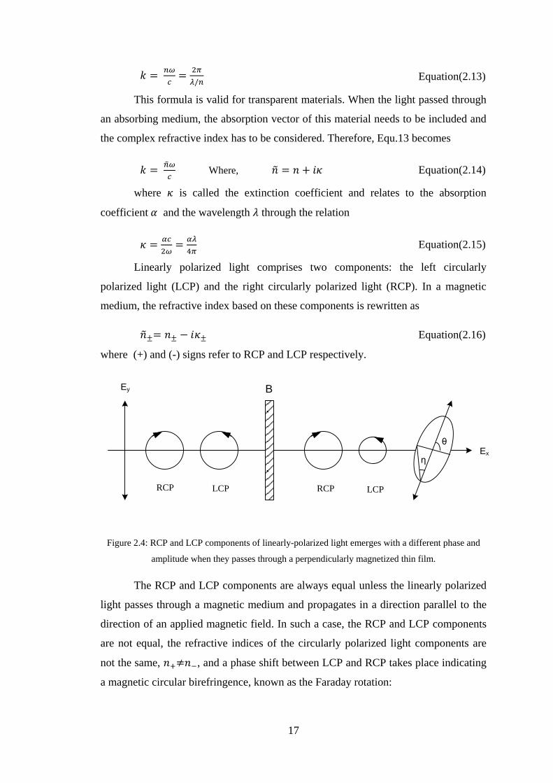
where (+) and (-) signs refer to RCP and LCP respectively.
RCP LCP RCP LCP
B
θ
ηEx
Ey
Figure 2.4: RCP and LCP components of linearly-polarized light emerges with a different phase and
amplitude when they passes through a perpendicularly magnetized thin film.
The RCP and LCP components are always equal unless the linearly polarized
light passes through a magnetic medium and propagates in a direction parallel to the
direction of an applied magnetic field. In such a case, the RCP and LCP components
are not equal, the refractive indices of the circularly polarized light components are
not the same, , and a phase shift between LCP and RCP takes place indicating
a magnetic circular birefringence, known as the Faraday rotation:
18
( ) Equation(2.17)
where is the speed of the light, and l is the thickness of the magnetic
medium. If the magnetic medium is absorbing light, the extinction coefficient
comprises two components. The extinction coefficient components for RCP and LCP
are respectivly. The difference between the extinction coefficient
components leads to elliptically polarized light, which gives the magnetic
circular dichroism ‘MCD’.
( ) Equation(2.18)
As a result, the transmitted or reflected light will be elliptically polarized and
rotated. This phenomenon is called the Faraday effect for transmitted light and the
Kerr effect for reflected light.
Fundamentally, the magneto optical effect is a result of the splitting of energy
levels in an external or spontaneous magnetic field. The absorption and the refractive
index are a result of the electric dipole transitions between the magnetically quantized
electronic states. Therefore, some spin-orbital coupling is necessary for the orbital
moment to reflect information about the magnetism. If the spin-orbit coupling is
weak, then the selection rules become and [5].
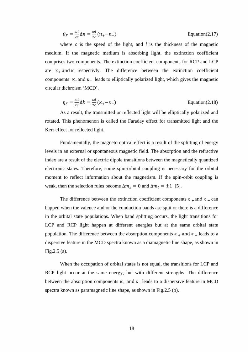
The difference between the extinction coefficient components can
happen when the valence and or the conduction bands are split or there is a difference
in the orbital state populations. When band splitting occurs, the light transitions for
LCP and RCP light happen at different energies but at the same orbital state
population. The difference between the absorption components leads to a
dispersive feature in the MCD spectra known as a diamagnetic line shape, as shown in
Fig.2.5 (a).
When the occupation of orbital states is not equal, the transitions for LCP and
RCP light occur at the same energy, but with different strengths. The difference
between the absorption components leads to a dispersive feature in MCD
spectra known as paramagnetic line shape, as shown in Fig.2.5 (b).
19
Figure 2.5: (a) Diamagnetic line shape and (b) Paramagnetic line shape of left and right circularly
polarized light transitions [42].
Paramagnetic and diamagnetic line shapes are historical labels unrelated to
earlier discussions in paramagnetism or diamagnetism. These line shapes could be
used to check whether the detected MCD signal is real or just an unreal signal caused
by a sample absorbing strongly at its band edge. This check could be performed by
examining the way in which a peak in the Faraday rotation is seen at the zero point of
an MCD signal and vice versa [43, 44].
Magneto-optical effects can occur at X-ray absorption edges, or resonances
due to the excitation of electrons in the conduction band enhanced by transitions from
atomic core levels to selected valence states; this kind of magneto optics is called the
XMCD [6].
2.12 Magneto-Optics in Terms of Dielectric Tensors
The propagation of electromagnetic waves is described by the dielectric tensor
or the conductivity tensor , which characterize the band-structure and describe the
electric displacement field in the material through .
The dielectric tensor describes the interaction of the different components of
an electromagnetic wave with the isotropic material through the dielectric tensor form
shown below:
(
) Equation(2.19)
20
If the material exhibits magnetic properties, the off diagonal components of
the dielectric tensor are activated; therefore, the propagation of electromagnetic waves
can be completely described by considering the complex dielectric tensor form shown
below:
(
) Equation(2.20)
In general, if the absorption of the material is not zero, the components of the
dielectric tensor became complex by considering the absorption vector component
and are given by
Equation(2.21)
The diagonal and off diagonal components of the dielectric tensor are
expressed in terms of the experimentally measured refractive index, absorption,
Faraday MCD and rotation through the formula
( ) Equation(2.22)
( )
Equation(2.23)
( ) Equation(2.24)
The diagonal and off diagonal components of the dielectric tensor can be
related to each other through the formulae
Equation(2.25)
√
√ Equation(2.26)
In the case of , magneto-optic effects are given in terms of the
difference between left- and right circular polarizations and therefore depend on
√ Equation(2.27)
The Faraday rotation, , and MCD, , in a sample of thickness are given
in terms of the real and imaginary parts, and , by:
(
( ))
( ) Equation(2.28)
21
( (
( ))) (
( ))
Equation(2.29)
which is equivalent to Equ.17 and Equ.18 mentioned previously.
2.13 Kramers-Kronig Relations
Kramers–Kronig relations are mathematical properties that connect the real
and imaginary parts of any complex response function. The Kramers–Kronig relations
allow us to calculate the real ( ) part of the complex refractive index ( ) from the
imaginary ( ) part (if known) at all frequencies, and vice versa [1]. Kramers-Kronig
relations are used to calculate the reflectivity ( ) from experimental ( ) and
( ) [45-47]. From another point of view, Kramers-Kronig transformations are used
to calculate the effective electron density and the imaginary part of the dielectric
constant from known ( ) [48, 49]. Kramers-Kronig analysis has been widely used
by others [49-52].
The Kramers-Kronig relations for the two components of the complex
dielectric function are [6]:
( )
∫
( )
Equation(2.30)
( )
∫
( )
Equation(2.31)
The Kramers–Kronig relations of the optical conductivity are as follows:
( )
∫
( )
Equation(2.32)
( )
∫
( )
Equation(2.33)
where (
) is the real (imaginary) part of the respectively [53]. The useful
forms related between the real and imaginary parts of the complex refractive index
are written as [1, 45]
( )
∫
( )
Equation(2.34)
22
( )
∫
( )
Equation(2.35)
where P indicates the Cauchy principal value of the integral [1, 53].
2.14 Pure In2O3
Indium oxide, In2O3, is a transparent material belonging to the wide band gap,
n-type semiconductors [54]. In2O3 grown in a low oxygen environment has a high
electron carrier concentration (between 1018
and 1020
cm-3
) [55, 56]. In2O3 is used
extensively in the semiconductor industry, especially in optoelectronics, including
displays, photovoltaics and light emitting diodes [57, 58]. Introducing tin to the In2O3
gives the form indium-tin-oxide, ITO, which is used widely as transparent electrodes
in liquid crystal display (LCD), and organic light emitting diode (OLED) devices [59,
60]. In2O3 crystallizes in a complex cubic bixbyite structure under the condition of O-
deficiency and high temperature. Otherwise, it will crystallize in an amorphous
structure. The complex cubic bixbyite structure contains 80 atoms in a unit cell with a
lattice parameter of 10.118Å [40, 56, 62, 65, 68, 73-75]. The complexity of the
structure originates from an array of unoccupied tetrahedral oxygen anion sites, which
can be viewed as surrounding face-centred in sites having a periodicity of one-half the
unit cell, or 5.059Å [76-79]. However, the cubic structure of In2O3 allows it to be
grown easily on low-cost substrates, such as MgO or Al2O3 for real applications [38].
In2O3 shows optical transitions from about 3.6 eV [61], 3.75eV [56, 62, 63], 3.5 - 4.3
eV [64-67] and transitions from about 2.62 eV [61, 64, 68-70] attributed to indirect
electronic transitions. However, the actual direct and indirect band gap energies of
In2O3 are remains contentious. Paul Erhart et al [71] and using density functional
theory calculations concluded that the experimental observations cannot be related to
the electronic structure of the defect free bulk material of In2O3. Aron Walsh et al
[68] found experimentally and theoretical agreement to set an upper limit of 2.9 eV
for the fundamental gap of In2O3 where the fundamental band gap 0.81 eV lower in
energy than the onset of strong optical absorption observed experimentally. The
calculated band structure of In2O3 is shown in Fig.2.6 (a), and the difference between
the fundamental and the optical energy gap are shown in Fig. 2.6 (b).

23
Figure 2.6: a) Band structure of In2O3 [68], b) Schematic diagrams for the fundamental and the optical
energy gap with the forbidden and allowed transitions in In2O3.
Fig.2.6 illustrated the band structure and Schematic diagrams for the
fundamental and optical energy gap with the forbidden and allowed transitions in
In2O3. Walsh report that, the optical transitions to the conduction band from all the
states above the ( ) state are forbidden because they have even parity. The optical
gap is 0.81eV higher than the real band gap which is observed by HXPS, which is
supported by Novkovski et al [72]. However there is a weak absorption was seen by
King et al. This might be because the transition was allowed because of defects or
because it was allowed because of phonons. We have seen a similar tail to the
absorption which depends on the oxygen vacancies. In our case, we believe that is
arises from transitions to the defect band because it is spin polarised as is seen in the
MCD. In addition, Novkovski et al reported several transitions from a direct
forbidden at 3.29 eV which is supported by F. Fuchs et al [69] and three indirect
allowed transitions at 2.09 eV, 3.42 eV and 3.58 eV. Therefore, the high conductivity
seen in In2O3 is due to the generation of carriers by transitions from the two lowest
maxima of the conduction band located within the valence band, going along with a
high transmission in the visible range, up to the photon energies above 4 eV, at which
direct allowed transitions occur, leading to strong absorption [72].
24
Studies on pure In2O3 thin films grown by various deposition techniques, such
as direct current (DC) reactive magnetron sputtering [80, 81], chemical vapour
deposition [82], reactive thermal evaporation [83], ion beam sputtering [84], and
pulsed laser deposition (PLD) [85], have revealed that the method of preparation and
growth conditions of complex oxide thin films play significant roles in their magnetic,
electrical and optical properties. For example, Qiao et al. deposited In2O3 films using
vacuum sputtering at a substrate temperature of 300K. The In2O3 films had an
amorphous structure and had low transparency and high resistivity [86]. Hichou et al.
deposited In2O3 films using pulse laser deposition (PLD) both at room temperature
and at 373 K. The In2O3 films deposited at room temperature showed an amorphous
structure whereas the In2O3 films deposited at 373 K had a cubic bixbyite structure
and the transmission factor increased with an increase in the deposition temperature
[87]. In addition, increasing the oxygen pressure led to an increase in the optical
transmission factor [88] and the optical transmission increased or decreased with an
impurity concentration [89], depending on the impurity type. The microstructure of
the In2O3 film changed with an increase in thickness, which led to some
improvements in the film’s properties. It was found that with an increase in thickness,
the electrical carrier density increases and the electrical resistivity decreases [86].
A previous study by Kaleemulla et al. about the influence of oxygen partial
pressure (PO2) on the physical properties of pure In2O3 revealed that the atomic ratio
of oxygen atoms to indium atoms decreased with a decrease in oxygen partial
pressure [90]. As a result, films prepared at low oxygen partial pressure are rich in
indium and oxygen vacancies. The grain size of pure In2O3 was found to decrease
with an increase in oxygen partial pressure, as reported by Ryzhikov et al. [91].
Ovadyahu et al. found that the films tend to show a dendritic growth and create too
many grain boundaries at low oxygen partial pressure [92]. Subramanyam et al., using
the X-ray diffraction, and Kaleemulla et al., using the EDAX spectrum analysis,
reported that the crystallinity of thin films increased with an increase in oxygen partial
pressure regardless of the material type or the growth method used [90, 93].
The transport properties of pure In2O3 at different oxygen partial pressures
were investigated by many groups. Choopun et al. reported that for thin films
deposited in an oxygen-rich environment, the carrier concentration and conductivity
were found to decrease with an increase in oxygen partial pressure due to the drop in
25
defect density [94]. Thin films deposited at low oxygen partial pressure usually fall
into the metallic regime where the carrier concentration reaches approximately 1020
electrons/cm3. Das et al., Bielz et al., Gupta et al., and others found that the electrical
resistivity and the Hall mobility increase with an increase in oxygen partial pressure
[90, 95-97]. Such variations in carrier concentration and electrical resistivity with
oxygen partial pressure were observed in Tin-doped indium oxide (ITO), as reported
by Kim et al. and Dekkers et al. [67, 98]. Kim found that the carrier density of the
ITO films increases from 2x10²⁰
to 11x1020
cm-3
when the oxygen deposition pressure
is decreased from 50 to 10 mTorr. This variation was confirmed by others such as
Ukah et al. [99], Liang et al. [100], and Subramanyam et al. [101].
Kaleemulla et al. found that the optical transmittance spectra increase with
increases of oxygen partial pressure. The enhancement in transmittance with an
increase in the oxygen partial pressure is also reported by other studies, such as H.
Kim et al. and B. Tahar et al. [102, 103]. Variations in the optical absorption
coefficient with oxygen partial pressure were found to increase with decreases in the
oxygen partial pressure due to the increase of oxygen vacancy defects density.
Another way to control the density of oxygen vacancy defects for already prepared
thin films is to use the annealing process approach. Many types of annealing process
have been used to enhance the physical properties of oxide thin films. Annealing in a
vacuum, in air, or in a specific gas environment are some of the annealing types that
are usually used. Annealing a thin film in air enhances the crystallization of the film
while annealing in a vacuum increases the oxygen vacancy density and, accordingly,
increases the carrier density. Increasing or decreasing the carrier density affects many
of the physical properties of thin films. The Fermi energy level may shift up or down,
and thin films may become insulator, semiconductors or metallic. It is widely believed
that the annealing process enhances the properties of thin films. However, while this
is true for un-doped materials, for doped materials, the annealing process is not
always desirable, as we will find in the following chapters. Vickraman et al. prepared
pure indium oxide (In2O3) thin films at the same growth conditions at base pressure
using an electron beam evaporation system [104]. Then, the thin films were annealed
in air at different temperatures, from 350 to 550 oC. The Variations in grain size and
lattice constant with annealing temperatures in air is shown in Fig.2.7.

26
Figure 2.7: Variations in grain size and lattice constant with annealing temperatures in air, (Data
plotted)[104].
Fig.2.7 illustrated the increase in grain size with an increase in the annealing
temperature which is due to the sufficient increase in the supply of thermal energy for
crystallization. The lattice constant was found to increase with an increase in the
annealing in air temperature, as shown in Fig.2.7 due to the decrease in oxygen
vacancies. The dislocation density and strain, were found to decrease with an increase
in the annealing in air temperature, as shown in Fig.2.8.
Figure 2.8: Variations in dislocation density and strain with annealing temperatures, (data plotted) [104].
The electrical resistivity was found to decrease with an increase in the
annealing temperature in air. The electrical conductivity of In2O3 films was found to
increase with an increase in the annealing temperature. These results show that the
mobility and/or carrier density increases with an increase in the annealing temperature
due to the fact that the free electrons are trapped in the grain boundaries. When the
grain size increases, as observed in Fig.2.7, the density of the grain boundaries

27
decreases; therefore, fewer carriers are trapped, leading to a higher carrier density or
an increased amount of released free carriers, which means higher conductivity and
lower resistivity [105]. Variations of the optical transmittance spectrum and the
optical band gap energy with annealing temperature are shown in Fig.2.9.
Figure 2.9: Variations in transmission spectrum and the optical band gap energy of pure In2O3 with
annealing temperatures in air,(Data plotted) [104].
The transmission spectrum of pure In2O3 film was found to increase with an
increase in the annealing temperature due to the enhancement in the crystallinity of
the films, which was also observed by Han et al. in ITO thin films [106]. The optical
band gap energy was found to increase with an increase in the annealing temperature,
as shown in Fig.2.9. The optical band gap shifted toward higher energy from 3.65 to
3.86 eV with an increase in the annealing temperature due to Burstein–Moss Effect.
Variations in the In2O3 index of refraction with annealing temperatures in air are
shown in Fig.2.10.
Figure 2.10: Variations in the index of refraction of In2O3 with annealing temperatures in air
(Data plotted) [104].
28
The increase of index of refraction from 1.84 to 1.91 with an increase in the
annealing temperature in air, implies that the stress in the lattice of In2O3 thin film
increases with increases in the annealing temperature. Growth of thin films in high
oxygen partial pressure or annealing them in air leads to fill up the empty positions in
the lattice with oxygen atoms. Therefore, the physical properties of pure In2O3 are
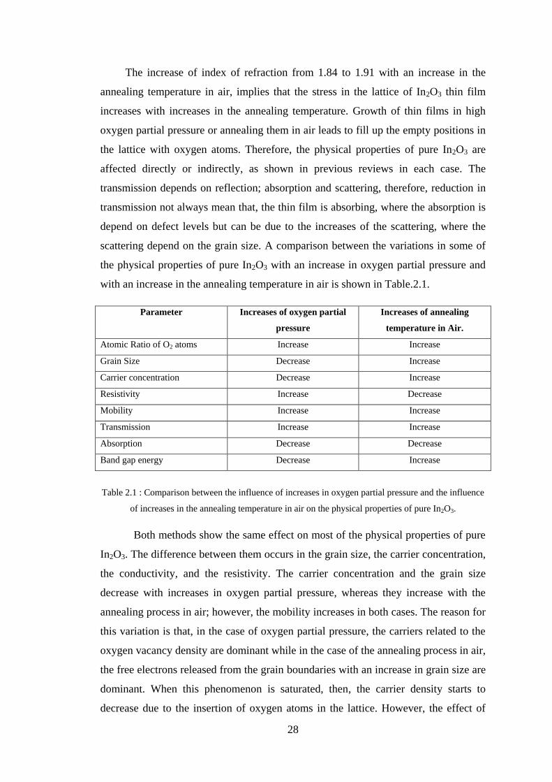
affected directly or indirectly, as shown in previous reviews in each case. The
transmission depends on reflection; absorption and scattering, therefore, reduction in
transmission not always mean that, the thin film is absorbing, where the absorption is
depend on defect levels but can be due to the increases of the scattering, where the
scattering depend on the grain size. A comparison between the variations in some of
the physical properties of pure In2O3 with an increase in oxygen partial pressure and
with an increase in the annealing temperature in air is shown in Table.2.1.
Parameter Increases of oxygen partial
pressure
Increases of annealing
temperature in Air.
Atomic Ratio of O2 atoms Increase Increase
Grain Size Decrease Increase
Carrier concentration Decrease Increase
Resistivity Increase Decrease
Mobility Increase Increase
Transmission Increase Increase
Absorption Decrease Decrease
Band gap energy Decrease Increase
Table 2.1 : Comparison between the influence of increases in oxygen partial pressure and the influence
of increases in the annealing temperature in air on the physical properties of pure In2O3.
Both methods show the same effect on most of the physical properties of pure
In2O3. The difference between them occurs in the grain size, the carrier concentration,
the conductivity, and the resistivity. The carrier concentration and the grain size
decrease with increases in oxygen partial pressure, whereas they increase with the
annealing process in air; however, the mobility increases in both cases. The reason for
this variation is that, in the case of oxygen partial pressure, the carriers related to the
oxygen vacancy density are dominant while in the case of the annealing process in air,
the free electrons released from the grain boundaries with an increase in grain size are
dominant. When this phenomenon is saturated, then, the carrier density starts to
decrease due to the insertion of oxygen atoms in the lattice. However, the effect of
29
oxygen vacancy density in this case is much lower than that in case of oxygen partial
pressure.
The sample thickness is another growth variable that has a large impact on the
structural, electrical, magnetic, optical, and magneto-optical properties of oxide thin
films. Increasing the thickness of a thin film is not always the right way to enhance its
properties. Determination of the thicknesses of a group of samples is essential in order
to investigate the effect of any physical parameter per volume and to compare these
samples. The influence of thickness on the physical properties of pure and doped
In2O3 has been investigated by many groups, whose findings will be summarized in
the following literature review. This section has been added in order to find out the
suitable thickness, for optical measurements, of thin films in the case of pure In2O3
and TM-doped In2O3.
Previous studies by Muranaka et al. and Kim et al. on the influence of
thickness on the physical properties of pure In2O3 revealed that the grain size of In2O3
thin films increase with an increase in thickness. The increment in grain size leads to a
reduction in the grain boundary scattering; consequently, the electrical resistivity of
the In2O3 thin film decreases [102, 107]. Liang et al. reported that the surface
roughness of In2O3 thin film increases with the increase in thickness due to the
increment in grain size, and the orientation of the film is an effective element to
control the roughness and, consequently, the grain size of In2O3 thin film [108, 109].
Qiao et al. found the strain that exists at the early stages of the growth process
decreases with an increase in thickness of In2O3 thin film [86].
The influence of thickness on the transport properties of In2O3 thin films was
investigated by several groups. Gupta et al. and Prathap et al. found that the carrier
concentration and mobility of In2O3 thin films increase with an increase in the
thickness [110, 111]. Al-Dahoudi et al. and Tak et al. reported the same results for
ITO thin films [109, 112]. The variations in resistivity, mobility and the carrier
concentration of un-doped In2O3 and Tin-doped In2O3 with thickness are shown in
Fig.2.11.

30
Figure 2.11: the variations in resistivity (ρ), carrier concentration (n), and mobility (µ) with thickness
of IO film (left) [110, 111], ITO film (right)[112].
Increases in the carrier density with increases in thickness due to increase of
oxygen vacancy density [113]. It has been reported that in thin films with a thickness
greater than 100nm, the carrier concentration decreases with an increase in thickness.
The reason given for this is that during the growth of the films, a large lattice strain is
presented by the mismatch between the substrate and the film, which causes many
defects. These defects act as traps and trap free electrons; as a result, the carrier
concentration decreases. Another reason given is because the oxygen vacancy density
decreases with an increase in thickness [113]. Liang et al. investigated the influence
of film thickness on the electro-optical properties of indium tin oxide films. They
found that the absorption coefficient increases rapidly with thickness due to the
increase in the carrier concentration. The optical absorption edge of Sn-doped In2O3
was found to shift towards higher energy with an increase in thickness. The variations
in optical band gap energy with an increase in thickness are also reported by Liang et
al. The optical band gap energy increased with increases in film thickness up to
500nm, and stabilized afterwards.
To date, there has been no optical study that considers the temperature
dependence of the absorption and transmittance for pure In2O3. Several optical studies
of un-doped In2O3 as a function of different growth conditions have been reported, but
all these studies have been taken at room temperature. Thus, the following literature
review discusses the optical properties of pure In2O3 at room temperature through a
published study about the substrate temperature dependence of optical properties of
un-doped In2O3. However, the dependence of other growth conditions will be covered
in this thesis. Prathap et al. investigated the optical properties of un-doped In2O3 at
31
different substrate temperatures in the range 300-400 oC. This gives us an indication
about the properties of our samples grown at 550 oC. The pure thin films of In2O3
were grown by spray pyrolysis technique [114] and the optical properties acquired
were at room temperature. The transmission spectra of pure In2O3 thin films deposited
at different substrate temperature and measured in the wavelengths between 300 and
2500 nm are shown in Fig.2.12.
Figure 2.12: Transmittance spectra of pure In2O3 films deposited at different substrate
temperatures[114].
The optical transmission decreases sharply near the absorption band edge of
In2O3. The absorption edge of In2O3 shifts towards higher energy with the increases in
the deposition temperature, indicating the widening of the band gap energy. In the
transparent region below the absorption edge, where , the spectra of the
film deposited at 400 oC displayed a transmittance higher than 80%. This suggests
that the density of defects decreases with an increase in the deposition temperature.
The absorption seen below the band gap edge for films deposited at 300 oC and 350
oC
in Fig.2.14 was attributed to the formation of defects. The defects presented in these
thin films are the oxygen vacancies, where there are no TM ions introduced to the
In2O3 matrix. Prathap et al. found the optical band gap and the index of refraction
varies with the temperature of the substrate, as shown in Fig.2.13.
32
Figure 2.13: Variations in the optical band gap energy and the refractive index of pure In2O3 with the
substrate temperatures [114].
The optical band gap energy of un-doped In2O3 thin film deposited at a
substrate temperature higher than 400 oC exceeds 3.60eV of energy. The optical band
gap energy shifts toward higher energy with an increase in the substrate temperature.
In Fig.2.13, the shoulder area below the band gap edge and located between 3.2eV
and 3.6eV for the thin film grown at 400 oC is the smallest compared with the other
shoulders, which confirmed the decrease in the density of defects with an increase in
the deposition temperature. The refractive index of pure In2O3 thin film deposited at a
substrate temperature higher than 400 oC is shown to be weakly energy dependent and
falls in the range of 1.8-1.95. The accurate refractive index spectrum of pure In2O3
thin film is very important in understanding the Faraday rotation and in achieving
correct results in many magneto-optics theoretical calculations, as we are going to
find out in the following chapters.
2.15 Sn doping In2O3 (ITO)
As we mentioned earlier, the crystal structure of pure In2O3 shows a cubic
bixbyite structure. X-ray diffraction (XRD) and transmission electron microscopy
(TEM) analyses reported by J. Popovicre et al. and S. Kim et al. revealed that doping
In2O3 with tin has no effect on the structure of In2O3; Sn-doped indium oxide samples
show a cubic bixbyite structure. The grain size decreases with increases in Sn doping
levels, but the lattice strain was found to increase with an increase in Sn content, as
shown in Fig.2.14 [115, 116].
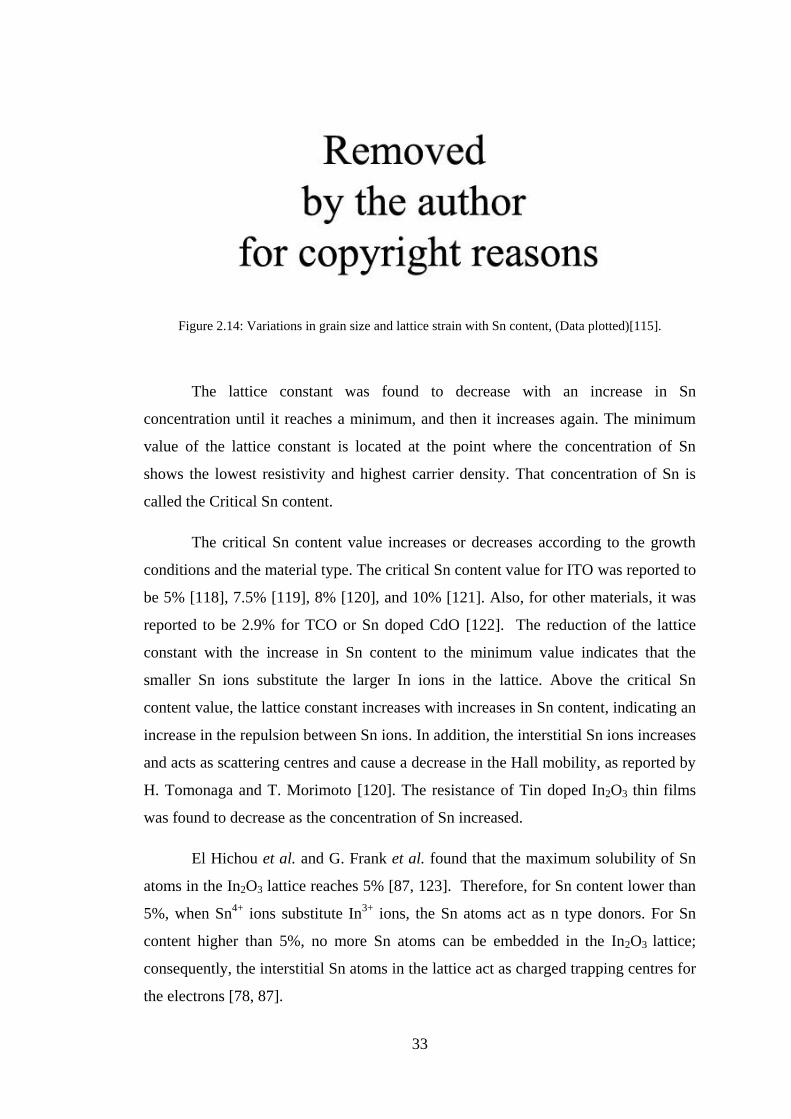
33
Figure 2.14: Variations in grain size and lattice strain with Sn content, (Data plotted)[115].
The lattice constant was found to decrease with an increase in Sn
concentration until it reaches a minimum, and then it increases again. The minimum
value of the lattice constant is located at the point where the concentration of Sn
shows the lowest resistivity and highest carrier density. That concentration of Sn is
called the Critical Sn content.
The critical Sn content value increases or decreases according to the growth
conditions and the material type. The critical Sn content value for ITO was reported to
be 5% [118], 7.5% [119], 8% [120], and 10% [121]. Also, for other materials, it was
reported to be 2.9% for TCO or Sn doped CdO [122]. The reduction of the lattice
constant with the increase in Sn content to the minimum value indicates that the
smaller Sn ions substitute the larger In ions in the lattice. Above the critical Sn
content value, the lattice constant increases with increases in Sn content, indicating an
increase in the repulsion between Sn ions. In addition, the interstitial Sn ions increases
and acts as scattering centres and cause a decrease in the Hall mobility, as reported by
H. Tomonaga and T. Morimoto [120]. The resistance of Tin doped In2O3 thin films
was found to decrease as the concentration of Sn increased.
El Hichou et al. and G. Frank et al. found that the maximum solubility of Sn
atoms in the In2O3 lattice reaches 5% [87, 123]. Therefore, for Sn content lower than
5%, when Sn4+
ions substitute In3+
ions, the Sn atoms act as n type donors. For Sn
content higher than 5%, no more Sn atoms can be embedded in the In2O3 lattice;
consequently, the interstitial Sn atoms in the lattice act as charged trapping centres for
the electrons [78, 87].
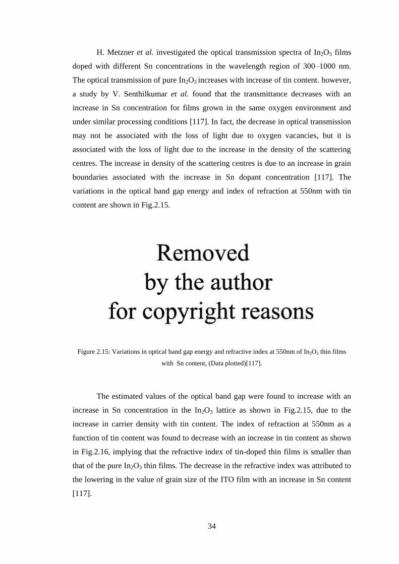
34
H. Metzner et al. investigated the optical transmission spectra of In2O3 films
doped with different Sn concentrations in the wavelength region of 300–1000 nm.
The optical transmission of pure In2O3 increases with increase of tin content. however,
a study by V. Senthilkumar et al. found that the transmittance decreases with an
increase in Sn concentration for films grown in the same oxygen environment and
under similar processing conditions [117]. In fact, the decrease in optical transmission
may not be associated with the loss of light due to oxygen vacancies, but it is
associated with the loss of light due to the increase in the density of the scattering
centres. The increase in density of the scattering centres is due to an increase in grain
boundaries associated with the increase in Sn dopant concentration [117]. The
variations in the optical band gap energy and index of refraction at 550nm with tin
content are shown in Fig.2.15.
Figure 2.15: Variations in optical band gap energy and refractive index at 550nm of In2O3 thin films
with Sn content, (Data plotted)[117].
The estimated values of the optical band gap were found to increase with an
increase in Sn concentration in the In2O3 lattice as shown in Fig.2.15, due to the
increase in carrier density with tin content. The index of refraction at 550nm as a
function of tin content was found to decrease with an increase in tin content as shown
in Fig.2.16, implying that the refractive index of tin-doped thin films is smaller than
that of the pure In2O3 thin films. The decrease in the refractive index was attributed to
the lowering in the value of grain size of the ITO film with an increase in Sn content
[117].
35
2.16 TM doped Oxides
Transition metal (TM) -doped semiconductor oxides have been found to show
ferromagnetism at room temperature [39, 124-132]. The ferromagnetism in semi
magnetic semiconductors (SMS) is usually attributed to the interaction between the
host s, p bands carriers and the localized 3d electrons in doped transition metal
elements. Several theoretical models have been suggested based on the s(p)-d
interactions feature, and these fall into two categories: the first category is the carrier-
mediated models like the Zener model and the Ruderman-Kittel-Kasuya-Yosida
(RKKY) model [133, 134]. In the carrier-mediated models, the coupling between
magnetic ions is achieved through the mobile carriers, i.e., holes in the valence band
or electrons in the conduction band. The second category is the super exchange
models like the double-exchange model [135-138]. In super exchange models, the
coupling is achieved between magnetic ions through the localized carriers.
The ferromagnetism in oxide magnetic semiconductors usually is induced by
clustered magnetic impurities [139] or attributed to the oxygen vacancy defects where
the ferromagnetic exchange interaction is mediated by shallow donor electrons
trapped in oxygen vacancy defects [125, 140]. The presence of metallic TM is always
expected, especially for Co-, and Fe-doped In2O3. Cobalt (Co) is one of the TMs that
show high total magnetic moments induced by each Co magnetic ion in the In2O3
matrix. The structural, magnetic, and electrical transport properties of Co-doped
indium oxide and indium-tin oxide thin films have been studied by several groups. J.
Stankiewicz et al. found different contributions of metallic Co and oxidized Co2+
to
the observed ferromagnetism and the uniform substitution of Co atoms seen in ITO
thin films doped with less than 7 % of Co [141, 142].
L. M. Huang et al. studied theoretically the magnetic and electronic properties
of the transition metal (V, Cr, Mn, Fe, Co, Ni, Cu) doped In2O3 and found that when
two TM ions of TM-TM are placed far from each other, only Co, Ni and Cu ions still
prefer the ferromagnetic orientation and the 3d bands show strong hybridization with
the host valence band formed mainly by the oxygen 2p state, while V, Cr, or Mn ions
prefer antiferromagnetic ordering and the 3d bands are merged with the conduction
band and show less hybridization with the host valence band [143].
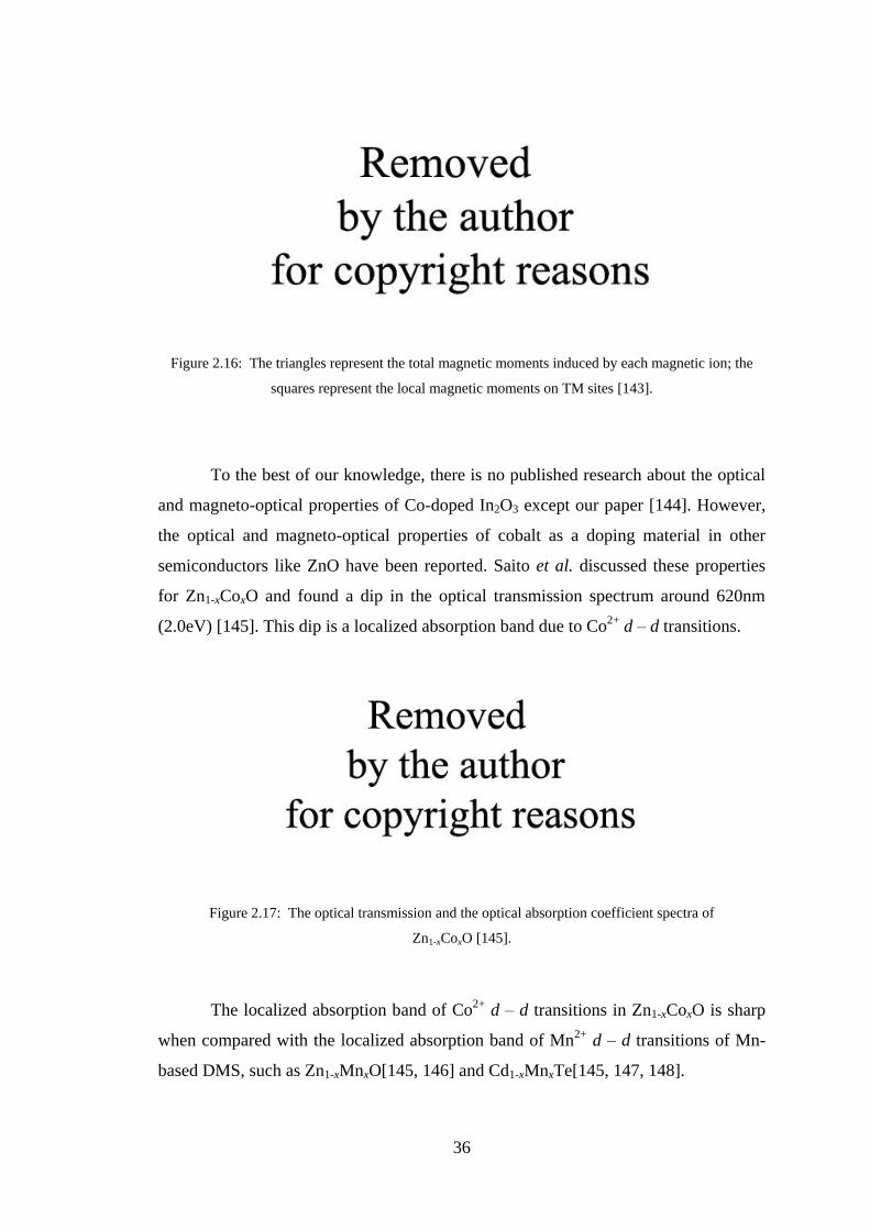
36
Figure 2.16: The triangles represent the total magnetic moments induced by each magnetic ion; the
squares represent the local magnetic moments on TM sites [143].
To the best of our knowledge, there is no published research about the optical
and magneto-optical properties of Co-doped In2O3 except our paper [144]. However,
the optical and magneto-optical properties of cobalt as a doping material in other
semiconductors like ZnO have been reported. Saito et al. discussed these properties
for Zn1-xCoxO and found a dip in the optical transmission spectrum around 620nm
(2.0eV) [145]. This dip is a localized absorption band due to Co2+
d – d transitions.
Figure 2.17: The optical transmission and the optical absorption coefficient spectra of
Zn1-xCoxO [145].
The localized absorption band of Co2+
d – d transitions in Zn1-xCoxO is sharp
when compared with the localized absorption band of Mn2+
d – d transitions of Mn-
based DMS, such as Zn1-xMnxO[145, 146] and Cd1-xMnxTe[145, 147, 148].
37
The MCD spectrum of Zn1-xCoxO shows an MCD spectral shape near 2.0 eV.
The MCD signal at 2.0eV for Co-doped semiconductors is related to the Co2+
d – d
transitions [145, 149-151]. Also, there is an MCD peak near the absorption edge of
the host semiconductor. The MCD spectrum of Zn1-xCoxO is strongly temperature
dependent. The MCD peak near the absorption edge of Zn1-xCoxO is negative at low
temperatures, and its magnitude rapidly decreases with an increase in temperature,
which reflects the paramagnetism of Co2+
ions in the host material; this, in turn, is
confirmed by XMCD measurements by Hakimi et al. in cobalt-doped indium tin
oxide thin films [152].
Figure 2.18: MCD of Zn1-xCoxO [145].
The polarity of the MCD and Faraday effect in real units can be used to reveal
whether the p–d interaction in DMS materials is ferromagnetic or antiferromagnetic.
It has been reported that Cd1-xMnxTe has a negative MCD peak polarity; therefore, the
p–d exchange interaction in Cd1-xMnxTe is antiferromagnetic [153]. This result is
adapted in Zn1-xCoxO where Zn1-xCoxO also has a negative MCD peak polarity; as a
result, the p–d exchange interaction in Zn1-xCoxO is antiferromagnetic, which is in
accordance with the results for other Co-based II–VI diluted magnetic semiconductors
such as Cd1-xCoxSe [154, 155]and Cd1-xCoxS [155] that have negative MCD peak
polarity, and confirms that the p–d exchange interaction in these materials is
antiferromagnetic. Most of the doped transition metals were found to exhibit very low
solubility in the host semiconductor’s lattice. Among them, Fe as a doping material
for In2O3 semiconductor exhibits an exceptional electrical conductivity, high Curie
38
temperature, high optical transparency, and high thermodynamic solubility reaching
more than 20% of Fe in the host matrix [156], which makes any observed
ferromagnetism intrinsic rather than originating in Fe clusters or any other magnetic
impurity phases [157]. Therefore, Fe doped In2O3 is considered to be one of the most
promising candidates for optoelectronics and spintronics applications.
An experimental study by D. Bérardan et al. on bulk Fe-doped In2O3 shows
that bulk Fe-doped In2O3 is paramagnetic due to Fe3+
ions, and the dominant
interactions are antiferromagnetic. For high iron content, a cluster glass or
superparamagnetic behaviour is observed [65]. S. Kohiki et al. investigated Fe-doped
In2O3 thin films and found that Fe-doped In2O3 thin films show antiferromagnetic
behaviour, which is attributed to the super exchange interaction between Fe3+
ions at p
and d sites [74]. Studies on Fe-doped In2O3 thin films by Yoo et al. and Peleckis et al.
show that Fe-doped In2O3 thin films exhibit ferromagnetic behaviour at room
temperature, which is attributed to the mixed valence of Fe2+
and Fe3+
[158, 159].
Another theoretical study by Hu et al. on the magnetic properties of Fe doped In2O3
shows that without oxygen vacancies, the doped Fe ions tend to display
antiferromagnetic spin ordering, and with oxygen vacancies, a shallow donor state is
induced and mediates the stable ferromagnetic exchange interaction [160]. Therefore,
the ferromagnetism observed in low-dimensionality samples in thin films or
nanocrystalline thin films is linked to different surface/volume ratios and therefore to
different oxygen vacancy concentrations.
2.17 Energy Levels of Oxygen Vacancies
Oxygen vacancies are found in any material that has oxygen atoms as a part of
its structure. The density of the oxygen vacancies varies based on the growth
conditions of that material. In an In2O3 crystal, the oxygen vacancy density increases
when the In2O3 crystal is grown at low oxygen pressure, as will be discussed later.
Sometimes, In2O3 crystals exhibit different crystallization qualities due to the
different amounts of oxygen vacancies and defects generated during growth. Such
differences lead to different transition paths. Therefore, In2O3 crystals show different
colours [161]. The oxygen vacancies in semiconductors induce the formation of new
energy levels within the band gap.
39
Figure 2.19: The PL spectrum of In2O3 nanowires at (a) as-grown In2O3 nanowires; (b) oxidized in air
at 850 oC for 3h; (c) deoxidized at 750 oC for 1 h [162].
Annealing in an oxygen rich atmosphere or reducing the atmosphere is an easy
way to change the concentration of surface oxygen vacancies. Wu et al. found that
oxidization and deoxidization of In2O3 by annealing the samples in air or in a vacuum
leads to the creation of energy levels due to the formation of oxygen vacancies [162].
The shallow oxygen vacancy states have been observed experimentally by
many groups [163-165]. The energy levels within the band gap induced by the oxygen
vacancies can be divided into two broad categories: near-band-edge (NBE) states and
deep-level (DL) states [166]. The DL states are ~ 0.6 eV below the conduction band
edge [167] and are reported to be 1.33eV below the conduction band edge [168].
Hauser et al. reported an oxygen vacancy transition at 0.3 eV below the conduction
band edge [169]. The NBE states are just below the conduction band edge. Cao et al.
reported that In2O3 nanowires formed NBE states at 0.01eV below the conduction
band edge [166]. Cao et al. found that the annealing process in air at a high
temperature (~600 °C for un-doped In2O3) decreases the impurities and structure
defects, such as oxygen vacancies. This leads to a high NBE emissions-to-DL-
emissions ratio [166]. Magdas et al. confirmed that In2O3 shows cathodoluminescence
spectra (CL) at 1.9, 2.6 eV as shown in Fig.2.20. The CL spectra at 1.9, 2.6 eV
attributed to DL oxygen deficiency states and the CL spectra at 3.1 eV attributed to
NBE oxygen deficiency states. After the annealing of samples in high vacuum
conditions, the high NBE emissions-to-DL-emissions ratio increases [170]. For doped
In2O3, the energy levels within the induced band gap may not be related to the oxygen
vacancies. G.W. Pabst et al. reported trap ionization energy of 0.65–0.8 eV, which
corresponds to the ionization of Fe2+
ions [171].
40
Figure 2.20: a) Cathodoluminescence (CL) spectrum of untreated In2O3 powder. b) CL spectrum after
annealing at 600 °C for 5 h. C) CL spectrum after annealing at 600 °C for 10 h.
b) and c) annealed in high vacuum conditions [170].
In this thesis, some of the Fe and Co doped In2O3 showed DL states found to
be related to the Fe3O4 and Co nanoparticles, which was confirmed by the XAFS
measurements. In fact, there are two methods to confirm the origin of the NBE states
and DL states. The first method is to use the XAFS measurement to check if there are
any nanoparticles. The second method is to anneal the samples in air. If the DL states
decrease with annealing, that implies that the DL states observed are due to the
oxygen vacancies. However, if the DL states increase, that implies that nanoparticles
of the doped material are formed and contribute to the physical properties detected.

41
2.18 References
1. M. Fox, Optical properties of solids. Oxford master series in condensed matter
physics 2001, Oxford ; New York: Oxford University Press. xii, 305 p.
2. M. Fox, Quantum optics : an introduction. Oxford master series in physics
2006, Oxford ; New York: Oxford University Press. xvii, 378 p.
3. B. D. Cullity, and C. D. Graham, Introduction to magnetic materials. 2nd ed
2009, Hoboken, N.J.: IEEE/Wiley. xvii, 544 p.
4. K. H. J. Buschow, and F. R. D. Boer, Physics of magnetism and magnetic
materials 2003, New York: Kluwer Academic/Plenum Publishers. vii, 182 p.
5. Y. B. Xu, and S.M. Thompson, Spintronic materials and technology. Series in
materials science and engineering 2007, New York: Taylor & Francis. 423 p.
6. V. Antonov, B. Harmon and A. Yaresko, Electronic structure and magneto-
optical properties of solids 2004, Dordrecht ; Boston: Kluwer Academic
Publishers. xiii, 528 p.
7. N. A. Spaldin, Magnetic materials : fundamentals and device applications
2003, Cambridge, Uk ; New York: Cambridge University Press. ix, 213 p.
8. Y. Liu, D. Shind and D. J. Sellmyer, Handbook of advanced magnetic
materials 2006, New York, Beijing: Springer ; Tsinghua University Press.
9. C. Kittel, Introduction to solid state physics. 7th ed 1996, New York: Wiley.
xi, 673 p.
10. S. A. Wolf, D. D. Awschalom, R. A. Buhrman, J. M. Daughton, S. V. Molnar,
M. L. Roukes, A. Y. Chtchelkanova and D. M. Treger, Science 294, 1488-
1495 (2001).
11. S. J. Pearton, Y. D. Park, C.R. Abernathy, M. E. Overberg, G. T. Thaler, J.
Kim, F. Ren, J. M. Zavada and R. G. Wilson, Thin Solid Films 447-448, 493-
501 (2004).
12. S. J. Pearton, C. R. Abernathy, D. P. Norton, A. F. Hebard, Y. D. Park, L. A.
Boatner and J.D. Budai, Materials Science and Engineering: R: Reports 40,
137-168 (2003).
13. A. H. MacDonald, P. Schiffer and N. Samarth, Nat Mater 4, 195-202 (2005).
42
14. K. Sato, K. Sato, Y. Furukawa and K. Nakajima, Crystal growth and
characterization of magnetic semiconductors, in Advances in Crystal Growth
Research 2001, Elsevier Science B.V.: Amsterdam. p. 303-319.
15. T. Kasuya, and A. Yanase, Reviews of Modern Physics 40, 684 (1968).
16. H. Ohno, Science 281, 951-956 (1998).
17. J. K. Furdyna, J. Appl. Phys. 64, R29-R64 (1988).
18. T. Dietl, H. Ohno, F. Matsukura, J. Cibert and D. Ferrand, Science 287, 1019-
1022 (2000).
19. K. Sato, and H. Katayama-Yoshida, Physica E: Low-dimensional Systems and
Nanostructures 10, 251-255 (2001).
20. U. Ozgur, Y. I. Alivov, C. Liu, A. Teke, M. A. Reshchikov, S. Dogan, V.
Avrutin, S. J. Cho and H. Morkoc, J. Appl. Phys. 98, 041301 (2005).
21. D. C. Look, B. Claflin, physica status solidi (b) 241, 624-630 (2004).
22. A. Haury, A. Wasiela, A. Arnoult, J. Cibert, S. Tatarenko, T. Dietl and Y. M.
d'Aubigné, Phys. Rev. Lett. 79, 511 (1997).
23. H. Ohno, J. Magn. Magn. Mater. 200, 110-129 (1999).
24. Y. Iye, A. Oiwa, A. Endo, S. Katsumoto, F. Matsukura, A. Shen, H. Ohno and
H. Munekata, Materials Science and Engineering B 63, 88-95 (1999).
25. H. Ohno, A. Shen, F. Matsukura, A. Oiwa, A. Endo, S. Katsumoto and Y. Iye,
Appl. Phys. Lett. 69, 363-365 (1996).
26. H. Ohno, H. Munekata, S. V. Molnar and L. L. Chang. New III-V diluted
magnetic semiconductors (invited). 1991. AIP.
27. H. Munekata, H. Ohno, S. V. Molnar, A. Segmüller, L. L. Chang and L. Esaki,
Phys. Rev. Lett. 63, 1849 (1989).
28. F. Matsukura, H. Ohno, A. Shen and Y. Sugawara, Phys. Rev. B 57, R2037
(1998).
29. M. E. Overberg, B. P. Gila, C. R. Abernathy, S. J. Pearton, N. A.
Theodoropoulou, K. T. McCarthy, S. B. Arnason and A. F. Hebard, Appl.
Phys. Lett. 79, 3128-3130 (2001).
30. X. Chen, M. Na, M. Cheon, S. Wang, H. Luo, B.D. McCombe, X. Liu, Y.
Sasaki, T. Wojtowicz, J. K. Furdyna, S. J. Potashnik and P. Schiffer, Appl.
Phys. Lett. 81, 511-513 (2002).

43
31. K. W. Edmonds, S. V. Novikov, M. Sawicki, R. P. Campion, C. R. Staddon,
A. D. Giddings, L. X. Zhao, K. Y. Wang, T. Dietl, C. T. Foxon and B. L.
Gallagher, Appl. Phys. Lett. 86, 152114 (2005).
32. S. V. Novikov, K. W. Edmonds, A. D. Giddings, K. Y. Wang, C. R. Staddon,
R. P. Campion, B. L. Gallagher and C. T. Foxon, Semicond. Sci. Technol.
L13 (2004).
33. T. S. Cheng, L. C. Jenkins, S. E. Hooper, C. T. Foxon, J. W. Orton and D. E.
Lacklison, Appl. Phys. Lett. 66, 1509-1511 (1995).
34. V. A. Chitta, J. A. H. Coaquira, J. R. L. Fernandez, C. A. Duarte, J. R. Leite,
D. Schikora, D. J. As, K. Lischka and E. Abramof, Appl. Phys. Lett. 85, 3777-
3779 (2004).
35. D. Schikora, M. Hankeln, D. J. As, K. Lischka, T. Litz, A. Waag, T. Buhrow
and F. Henneberger, Phys. Rev. B 54, R8381 (1996).
36. J. Philip, A. Punnoose, B. I. Kim, K. M. Reddy, S. Layne, J. O. Holmes, B.
Satpati, P. R. LeClair, T. S. Santos and J. S. Moodera, Nat Mater 5, 298-304
(2006).
37. R. P. Panguluri, P. Kharel, C. Sudakar, R. Naik, R. Suryanarayanan, V. M.
Naik, A. G. Petukhov, B. Nadgorny and G. Lawes, Phys. Rev. B 79, 165208
(2009).
38. N. H. Hong, J. Sakai, N. T. Huong and V. Brize, Appl. Phys. Lett. 87, 102505-
3 (2005).
39. G. Peleckis, X. Wang and S. X. Dou, Appl. Phys. Lett. 89, 022501 (2006).
40. N. H. Hong, J. Sakai, N. T. Huong and V. Brizé, J. Magn. Magn. Mater. 302,
228-231 (2006).
41. G.A. Gehring, H. J. Blythe, F. Qi, D. S. Score, A. Mokhtari, M. Alshammari,
M.S. Al Qahtani and A.M. Fox, Magnetics, IEEE Transactions on 46, 1784-
1786 (2010).
42. A. Behan, Characterisation of Doped ZnO Thin Films for Spintronic
Applications, in Department of Physics and Astronomy 2008, The University
of Sheffield
43. J. Suits, Magnetics, IEEE Transactions on 8, 95-105 (1972).
44. S. Wittekoek, T. J. A. Popma, J. M. Robertson and P. F. Bongers, Phys. Rev.
B 12, 2777 (1975).
44
45. F. Wooten, Optical properties of solids 1972, New York,: Academic Press.
xii, 260 p.
46. E. D. Palik, Handbook of optical constants of solids. Academic Press
handbook series 1985, Orlando: Academic Press. xviii, 804 p.
47. J. R. McBride, L. R. Miller and W. H. Weber, Phys. Rev. B 49, 12224
(1994).
48. S. Tajima, H. Ishii, T. Nakahashi, T. Takagi, S. Uchida, M. Seki, S. Suga, Y.
Hidaka, M. Suzuki, T. Murakami, K. Oka and H. Unoki, Journal of the Optical
Society of America B: Optical Physics 6, 475-482 (1989).
49. A. I. Kozlov, S. G. K., and V. V. Sobolev, Moldavian Journal of the Physical
Sciences 4, 5 (2005).
50. F. J. Kahn, P. S. Pershan and J. P. Remeika, Phys. Rev. 186, 891 (1969).
51. W. Beckenbaugh, J. Evers, G. Güntherodt, E. Kaldis and P. Wachter, J. Phys.
Chem. Solids 36, 239-248 (1975).
52. S. K. Park, T. Ishikawa and Y. Tokura, Phys. Rev. B 58, 3717 (1998).
53. H. Czichos, T. Saito and L.R. Smith, Springer handbook of materials
measurement methods 2006, [Germany]: Springer. xxvi, 1208 p.
54. D. Zhang, C. Li, S. Han, X. Liu, T. Tang, W. Jin and C. Zhou, Vol. 82. 2003:
AIP. 112-114.
55. J. Stankiewicz, F. Villuendas and R. Alcala, Appl. Phys. Lett. 96, 192108
(2010).
56. S. J. Pearton, C. R. Abernathy, M. E. Overberg, G. T. Thaler, D. P. Norton, N.
Theodoropoulou, A. F. Hebard, Y. D. Park, F. Ren, J. Kim and L. A. Boatner,
J. Appl. Phys. 93, 1-13 (2003).
57. C. N. D. Carvalho, G. Lavareda, A. Amaral, O. Conde and A.R. Ramos,
Journal of Non-Crystalline Solids 352, 2315-2318 (2006).
58. J. H. Lee, S. Y. Lee and B. O. Park, Materials Science and Engineering: B
127, 267-271 (2006).
59. H. Han, J. W. Mayer and T. L. Alford, J. Appl. Phys. 99, 123711 (2006).
60. H. Han, D. Adams, J. W. Mayer and T. L. Alford, J. Appl. Phys. 98, 083705
(2005).
45
61. D. Beena, K. J. Lethy, R. Vinodkumar, V. P. M. Pillai, V. Ganesan, D. M.
Phase and S. K. Sudheer, Applied Surface Science 255, 8334-8342 (2009).
62. F. X. Jiang, X. H. Xu, J. Zhang, H. S. Wu and G.A. Gehring, Applied Surface
Science 255, 3655-3658 (2009).
63. I. Hamberg, C. G. Granqvist, K. F. Berggren, B. E. Sernelius and L. Engström,
Phys. Rev. B 30, 3240 (1984).
64. R. L. Weiher, and R. P. Ley, J. Appl. Phys. 37, 299-302 (1966).
65. D. Bérardan, and E. Guilmeau, J. Phys.: Condensed Matter 19, 236224
(2007).
66. H. Kim, A. Pique, J. S. Horwitz, H. Mattoussi, H. Murata, Z. H. Kafafi and D.
B. Chrisey, Appl. Phys. Lett. 74, 3444-3446 (1999).
67. H. Kim, C. M. Gilmore, A. Pique, J. S. Horwitz, H. Mattoussi, H. Murata, Z.
H. Kafafi and D. B. Chrisey, J. Appl. Phys. 86, 6451-6461 (1999).
68. A. Walsh, J. L. F. Da Silva, S. H. Wei, C. Körber, A. Klein, L. F. J. Piper, A.
DeMasi, K. E. Smith, G. Panaccione, P. Torelli, D. J. Payne, A. Bourlange and
R. G. Egdell, Phys. Rev. Lett. 100, 167402 (2008).
69. F. Fuchs, and F. Bechstedt, Phys. Rev. B 77, 155107 (2008).
70. P. D. C. King, T. D. Veal, D. J. Payne, A. Bourlange, R. G. Egdell and C. F.
McConville, Phys. Rev. Lett. 101, 116808 (2008).
71. P. Erhart, A. Klein, R. G. Egdell and K. Albe, Phys. Rev. B 75, 153205
(2007).
72. N. Novkovski, and A. Tanuševski, Semicond. Sci. Technol. 23, 095012
(2008).
73. M. Marezio, Acta Crystallographica 20, 723-728 (1966).
74. S. Kohiki, M. Sasaki, Y. Murakawa, K. Hori, K. Okada, H. Shimooka, T.
Tajiri, H. Deguchi, S. Matsushima, M. Oku, T. Shishido, M. Arai, M. Mitome
and Y. Bando, Thin Solid Films 505, 122-125 (2006).
75. J. Chandradass, M. Balasubramanian, S. Kumar, D. S. Bae and K. H. Kim,
Current Appl. Phys. 10, 333-336 (2010).
76. F. O. Adurodija, H. Izumi, T. Ishihara, H. Yoshioka, H. Matsui and M.
Motoyama, Appl. Phys. Lett. 74, 3059-3061 (1999).
46
77. E. J. Tarsa, J. H. English and J. S. Speck, Appl. Phys. Lett. 62, 2332-2334
(1993).
78. I. Hamberg, and C. G. Granqvist, J. Appl. Phys., 1986. 60, R123-R160 DOI:
10.1063/1.337534.
79. T. B. Hur, I. J. Lee, H. L. Park, Y. H. Hwang and H. K. Kim, Solid State
Commun. 130, 397-400 (2004).
80. A. N. H. Al-Ajili, and S. C. Bayliss, Thin Solid Films 305, 116-123 (1997).
81. S. Kasiviswanathan, and G. Rangarajan, J. Appl. Phys. 75, 2572-2577 (1994).
82. S. Suh, and D.M. Hoffman, Journal of the American Chemical Society 122,
9396-9404 (2000).
83. C. A. Pan, and T. P. Ma, Appl. Phys. Lett. 37, 163-165 (1980).
84. J. S. Cho, K. H. Yoon and S. K. Koh, J. Appl. Phys. 89, 3223-3228 (2001).
85. E. J. Tarsa, J. H. English and J. S. Speck, Appl. Phys. Lett. 62, 2332-2334
(1993).
86. Z. Qiao, R. Latz and D. Mergel, Thin Solid Films 466, 250-258 (2004).
87. A. El Hichou, A. Kachouane, J. L. Bubendorff, M. Addou, J. Ebothe, M.
Troyon and A. Bougrine, Thin Solid Films 458, 263-268 (2004).
88. S. H. Kim, N.M. Park, T. Kim and G. Sung, Thin Solid Films 475, 262-266
(2005).
89. S. M. Rozati, and T. Ganj, Renewable Energy 29, 1671-1676 (2004).
90. S. Kaleemulla, A. S. Reddy, S. Uthanna and P.S. Reddy, Journal of Alloys and
Compounds 479, 589-593 (2009).
91. A. S. Ryzhikov, R. B. Vasiliev, M. N. Rumyantseva, L. I. Ryabova, G. A.
Dosovitsky, A. M. Gilmutdinov, V. F. Kozlovsky and A. M. Gaskov,
Materials Science and Engineering B 96, 268-274 (2002).
92. Z. Ovadyahu, B. Ovryn and H.W. Kraner, Journal of The Electrochemical
Society 130, 917-921 (1983).
93. T. K. Subramanyam, B. S. Naidu and S. Uthanna, Appl. Surf. Sci. 169-170,
529-534 (2001).
94. S. Choopun, R. D. Vispute, W. Noch, A. Balsamo, R. P. Sharma, T.
Venkatesan, A. Iliadis and D. C. Look, Appl. Phys. Lett. 75, 3947-3949
(1999).
47
95. R. Das, K. Adhikary and S. Ray, Appl. Surf. Sci. 253, 6068-6073 (2007).
96. T. Bielz, H. Lorenz, W. Jochum, R. Kaindl, . lauser, . l t er and .
Penner, J. Phys. Chem. C 114, 9022-9029 (2010).
97. R. K. Gupta, K. Ghosh, S. R. Mishra and P. K. Kahol, Appl. Surf. Sci. 254,
4018-4023 (2008).
98. J. M. Dekkers, G. Rijnders and D. H. A. Blank, Appl. Phys. Lett. 88, 151908-
3 (2006).
99. N. B. Ukah, R. K. Gupta, P.K. Kahol and K. Ghosh, Appl. Surf. Sci. 255,
9420-9424 (2009).
100. Y. C. Liang, and Y. C. Liang, Appl. Phys. A: Materials Science &
Processing 97, 249-255 (2009).
101. T. K. Subramanyam, B. R. Krishna, S. Uthanna, B. S. Naidu and P. J. Reddy,
Vacuum 48, 565-569 (1997).
102. H. Kim, J. S. Horwitz, G. P. Kushto, S. B. Qadri, Z. H. Kafafi and D. B.
Chrisey, Appl. Phys. Lett. 78, 1050-1052 (2001).
103. R. B. H. Tahar, T. Ban, Y. Ohya, and Y. Takahashi, J. Appl. Phys. 83, 2631
(1998).
104. V. Senthilkumar, and P. Vickraman, Current Appl. Phys. 10, 880-885 (2010).
105. H. R. Fallah, M. Ghasemi, A. Hassanzadeh and H. Steki, Materials Research
Bulletin 42, 487-496 (2007).
106. H. Han, J. W. Mayer and T. L. Alford, J. Appl. Phys. 100, 083715 (2006).
107. S. Muranaka, and N. Hayashi, Journal of Materials Science 44, 3315-3318
(2009).
108. C. H. Liang, S. C. Chen, X. Qi, C. S. Chen and C. C. Yang, Thin Solid Films
519, 345-350 (2010).
109. Y. H. Tak, K. B. Kim, H. G. Park, K. H. Lee and J. R. Lee, Thin Solid Films
411, 12-16 (2002).
110. R. K. Gupta, K. Ghosh, R. Patel and P. K. Kahol, Appl. Surf. Sci. 255, 3046-
3048 (2008).
111. P. Prathap, N. Revathi, K. T. R. Reddy and R. W. Miles, Thin Solid Films
518, 1271-1274 (2009).
112. N. Al-Dahoudi, and M. A. Aegerter, Thin Solid Films 502, 193-197 (2006).

48
113. K. Vanheusden, , C. H. Seager, W. L. Warren, D. R. Tallant and J. A. Voigt,
Appl. Phys. Lett. 68, 403-405 (1996).
114. P. Prathap, Y. P. V. Subbaiah, M. Devika and K. T. R. Reddy, Materials
Chemistry and Physics 100, 375-379 (2006).
115. J. Popovic, B. Grzeta, E. Tkalcec, A. Tonejc, M. Bijelic and C. Goebbert,
Materials Science and Engineering: B 176, 93-98 (2011).
116. S. M. Kim, K. H. Seo, J. H. Lee, J. J. Kim, H. Y. Lee and J. S. Lee, Journal of
the European Ceramic Society 26, 73-80 (2006).
117. V. Senthilkumar, P. Vickraman, M. Jayachandran and C. Sanjeeviraja,
Vacuum 84, 864-869 (2010).
118. S. M. A. Durrani, E. E. Khawaja, J. Shirokoff, M. A. Dams, G. D. Khattak, M.
A. Salim and M. S. Hussain, Solar Energy Materials and Solar Cells 44, 37-47
(1996).
119. J. Kanazawa, T. Haranoh and K. Matsumoto, Vacuum 41, 1463-1465 (1990).
120. H. Tomonaga, and T. Morimoto, Thin Solid Films 392, 243-248 (2001).
121. M. J. Alam, and D. C. Cameron, Thin Solid Films 377-378, 455-459 (2000).
122. B. J. Zheng, J. S. Lian, L. Zhao and Q. Jiang, Vacuum 85, 861-865 (2011).
123. G. Frank, H. Köstlin and A. Rabenau, physica status solidi (a) 52, 231-238
(1979).
124. N. H. Hong, J. Sakai, W. Prellier and A. Hassini, J. Phys.: Condensed Matter
17, 1697 (2005).
125. J. M. D. Coey, A. P. Douvalis, C. B. Fitzgerald and M. Venkatesan, Appl.
Phys. Lett. 84, 1332-1334 (2004).
126. S. B. Ogale, R. J. Choudhary, J. P. Buban, S. E. Lofland, S. R. Shinde, S. N.
Kale, V. N. Kulkarni, J. Higgins, C. Lanci, J. R. Simpson, N. D. Browning, S.
D. Sarma, H. D. Drew, R. L. Greene and T. Venkatesan, Phys. Rev. Lett. 91,
077205 (2003).
127. M. Venkatesan, C. B. Fitzgerald, J. G. Lunney and J. M. D. Coey, Phys. Rev.
Lett. 93, 177206 (2004).
128. N. H. Hong, J. Sakai, W. Prellier, A. Hassini, A. Ruyter and F. Gervaism,
Phys. Rev. B 70, 195204 (2004).
49
129. Z. Wang, J. Tang, L. D. Tung, W. Zhou and L. Spinu, J. Appl. Phys. 93, 7870-
7872 (2003).
130. G. Peleckis, X. L. Wang and S. X. Dou, J. Magn. Magn. Mater. 301, 308-311
(2006).
131. P. F. Xing, Y. X. Chen, M. J. Tang, S. S. Yan, G. L. Liu, L. M. Mei and J. Jun,
Chinese Physics Letters 26, 117503 (2009).
132. X. Meng, L. Tang and J. Li, J. Phys. Chem. C 114, 17569-17573 (2010).
133. T. Dietl, H. Ohno and F. Matsukura, Phys. Rev. B 63, 195205 (2001).
134. T. Dietl, A. Haury, Y. M. d'Aubign, Phys. Rev. B 55, R3347 (1997).
135. H. Akai, Phys. Rev. Lett. 81, 3002 (1998).
136. P. G. D. Gennes, Phys. Rev. 118, 141 (1960).
137. M. V. Schilfgaarde, and O. N. Mryasov, Phys. Rev. B 63, 233205 (2001).
138. P. W. Anderson, and H. Hasegawa, Phys. Rev. 100, 675 (1955).
139. J. Y. Kim, J. H. Park, B. G. Park, H.J. Noh, S. J. Oh, J. S. Yang, D. H. Kim, S.
D. Bu, T. W. Noh, H. J. Lin, H. H. Hsieh and C. T. Chen, Phys. Rev. Lett. 90,
017401 (2003).
140. J. M. D. Coey, M. Venkatesan and C. B. Fitzgerald, Nat Mater 4, 173-179
(2005).
141. G. Subías, J. Stankiewicz, F. Villuendas, M. P. Lozano and J. García1, Phys.
Rev. B 79, 094118 (2009).
142. J. Stankiewicz, F. Villuendas and J. Bartolomé, Phys. Rev. B 75, 235308
(2007).
143. L. M. Huang, C. M. Araújo and R. Ahuja, EPL (Europhysics Letters) 87,
27013 (2009).
144. A. M. H. R. Hakimi, M. G. Blamire, S. M. Heald, M. S. Alshammari, M. S.
Alqahtani, D. S. Score, H. J. Blythe, A. M. Fox and G. A. Gehring, Phys. Rev.
B 84, 085201 (2011).
145. K. Ando, H. Saito, Z. Jin, T. Fukumura, M. Kawasaki, Y. Matsumoto and H.
Koinuma, Vol. 78. 2001: AIP. 2700-2702.
146. T. Fukumura, Z. Jin, A. Ohtomo, H. Koinuma and M. Kawasaki, Vol. 75.
1999: AIP. 3366-3368.
147. K. Ando, Phys. Rev. B 47, 9350 (1993).
50
148. Y. R. Lee, and A. K. Ramdas, Solid State Commun. 51, 861-863 (1984).
149. H. A. Weakliem, Vol. 36. 1962: AIP. 2117-2140.
150. J. M. Baranowski, J. W. Allen and G. L. Pearson, Phy. Rev. 160, 627 (1967).
151. K. Ando, A. Chiba and H. Tanoue, Vol. 83. 1998: AIP. 6545-6547.
152. Hakimi, A. M. H. R., F. Schoofs, R. Bali, N. A. Stelmashenko, M. G. Blamire,
S. Langridge, S. A. Cavill, G. V. D. Laan and S. S. Dhesi, Phys. Rev. B 82,
144429 (2010).
153. K. Ando, and H. Akinaga, J. Magn. Magn. Mater. 140-144, Part 3, 2029-2030
(1995).
154. M. Nawrocki, F. Hamdani, J. P. Lascaray, Z. Golacki and J. Deportes, Solid
State Commun. 77, 111-114 (1991).
155. U. Gennser, X. C. Liu, T. Q. Vu, D. Heiman, T. Fries, Y. Shapira, M.
Demianiuk and A. Twardowski, Phys. Rev. B 51, 9606 (1995).
156. Z. G. Yu, J. He, S. Xu, Q. Xue, O. M. J. van't Erve, B. T. Jonker, M. A.
Marcus, Y. K. Yoo, S. Cheng and X. D. Xiang, Phys. Rev. B 74, 165321
(2006).
157. P. F. Xing, Y. X. Chen, S. S. Yan, G. L. Liu, L. M. Mei, K. Wang, X. D. Han
and Z. Zhang, Appl. Phys. Lett. 92, 022513 (2008).
158. Y. K. Yoo, Q. Xue, H. C. Lee, S. Cheng, X. D. Xiang, G. F. Dionne, S. Xu, J.
He, Y. S. Chu, S. D. Preite, S. E. Lofland and I. Takeuchi, Appl. Phys. Lett.
86, 042506 (2005).
159. G. Peleckis, X. L. Wang and S. X. Dou, Appl. Phys. Lett. 88, 132507-3
(2006).
160. S. J. Hu, S. S. Yan, X. I. Lin, X. X. Yao, Y. X. Chen, G. I. Liu and L. M. Mei,
Appl. Phys. Lett. 91, 262514-3 (2007).
161. C. P. Chu, T. S. Ko, Y. C. Chang, T. C. Lu, H. C. Kuo and S. C. Wang,
Materials Science and Engineering: B 147, 276-279 (2008).
162. W. Ping, Q. Li, X. Zou, W. Cheng, D. Zhang, C. Zhao, L. Chi and T. Xiaoand,
J. of Physics: Conference Series 188, 012054 (2009).
163. C. Wang, M. Takahashi, H. Fujino, X. Zhao, E. Kume, T. Horiuchi and S.
Sakai, J. Appl. Phys. 99, 054104 (2006).
51
164. H. Yang, M. Jain, N. A. Suvorova, H. Zhou, H. M. Luo, D. M. Feldmann, P.
C. Dowden, R. F. DePaula, S. R. Foltyn and Q. X. Jia, Appl. Phys. Lett. 91,
072911 (2007).
165. H. W. Jang, S. H. Baek, D. Ortiz, C. M. Folkman, C. B. Eom, Y. H. Chu, P.
Shafer, R. Ramesh, V. Vaithyanathan and D. G. Schlom, Appl. Phys. Lett. 92,
062910 (2008).
166. H. Cao, X. Qiu, Y. Liang, Q. Zhu and M. Zhao, Appl. Phys. Lett. 83, 761-763
(2003).
167. S. J. Clark, and J. Robertson, Appl. Phys. Lett. 2009. 94, 022902.
168. Z. Zhang, P. Wu, L. Chen and J. Wang, Appl. Phys. Lett. 96, 232906 (2010).
169. A. J. Hauser, J. Zhang, L. Mier, R. A. Ricciardo, P. M. Woodward, T. L.
Gustafson, L. J. Brillson and F. Y. Yang, Appl. Phys. Lett. 92, 222901-3
(2008).
170. D. A. Magdas, A. Cremades and J. Piqueras, Appl. Phys. Lett. 88, 113107
(2006).
171. G. W. Pabst, L. W. Martin, Y. H. Chu and R. Ramesh, Appl. Phys. Lett. 90,
072902 (2007).
172. A. Y. Polyakov, A. V. Govorkov, N. B. Smirnov, N. Y. Pashkova, G. T.
Thaler, M. E. Overberg, R. Frazier, C. R. Abernathy, S. J. Pearton, J. Kim and
F. Ren, J. Appl. Phys. 92, 4989-4993 (2002).
173. R. Y. Korotkov, J. M. Gregie and B. W. Wessels, Appl. Phys. Lett. 80, 1731-
1733 (2002).
174. P. G. Baranov, I. V. Ilyin, E. N. Mokhov and A. D. Roenkov, Semicond. Sci.
Technol. 11, 1843 (1996).
175. M. A. Khan, D. T. Olson, J. N. Kuznia, W. E. Carlos and J. A. Freitas, J. Appl.
Phys. 74, 5901-5903 (1993).
176. J. Baur, K. Maier, M. Kunzer, U. Kaufmann and J. Schneider, Appl. Phys.
Lett. 65, 2211-2213 (1994).
177. J. Baur, K. Maier, M. Kunzer, U. Kaufmann, J. Schneider, H. Amano, I.
Akasaki, T. Detchprohm and K. Hiramatsu, Appl. Phys. Lett. 64, 857-859
(1994).
178. E. Burstein, Phys. Rev. 93, 632 (1954).
52
Chapter 3 – Experimental Setup and Techniques
3.1 Introduction
This chapter explores the experimental techniques employed in this work and
the procedures followed to analyze the presented data. The samples used in this thesis
were grown by our group here in the University of Sheffield or obtained through the
collaboration of our group with many groups in same field. These groups are Xiao-
Hong Xu’s group from Shanxi Normal University, China; A. M. H. R. Hakimi from
the University of Cambridge; KACST group from Saudi Arabia; and Ya. Mukovskii’s
group from the National University of Science and Technology “MISiS”, Russia. The
source of the samples will be mentioned in every section throughout this thesis. My
main duty in our group was to investigate the optical and magneto-optics properties of
the samples that we grew or obtained. The first section of this chapter deals with the
magneto-optics spectroscopy technique. It covers the fundamentals and the
operational principle of the magneto-optical spectroscopy. Also, it explains the
procedures used to measure the magneto-optics properties of the samples. The second
section deals with the absorption spectroscopy technique and gives an overview of the
absorption spectroscopy. Also, it explains the procedures used to measure the optical
properties of the samples, such as the transmission, reflection, and absorption. It
explains how these data were used to determine the band gap energy of the sample.
The third section describes the growth techniques used to fabricate the samples and
the last section describes the procedures used to determine the film thickness and the
refractive index of the samples.
3.2 Magneto-Optics Setup and the Principles of the Technique
Katsuaki Sato [1] developed the measurements of magneto-optical spectra by
using a Piezo-Birefringent Modulator. This approach is considered one of the most
advanced magneto-optical techniques and is widely used [2-16]. Sato’s technique
allows the simultaneous determination of magnetic circular dichroism (MCD) and
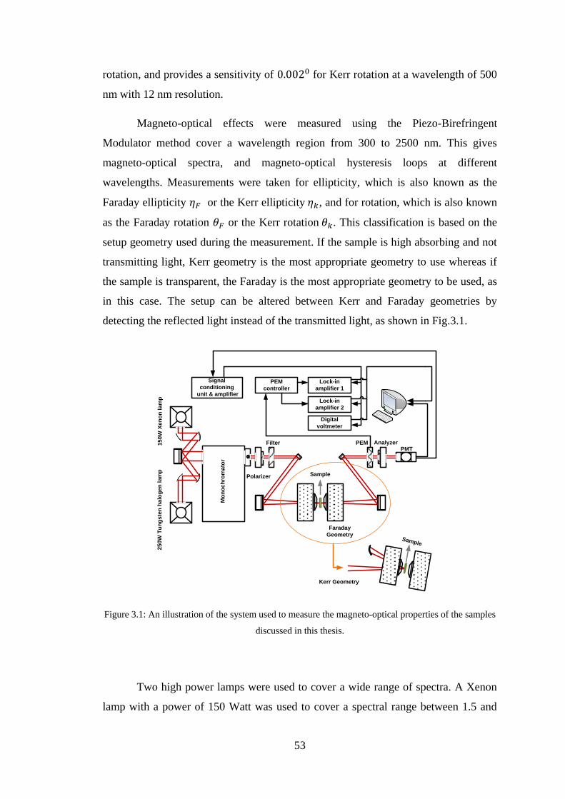
53
rotation, and provides a sensitivity of for Kerr rotation at a wavelength of 500
nm with 12 nm resolution.
Magneto-optical effects were measured using the Piezo-Birefringent
Modulator method cover a wavelength region from 300 to 2500 nm. This gives
magneto-optical spectra, and magneto-optical hysteresis loops at different
wavelengths. Measurements were taken for ellipticity, which is also known as the
Faraday ellipticity or the Kerr ellipticity , and for rotation, which is also known
as the Faraday rotation or the Kerr rotation . This classification is based on the
setup geometry used during the measurement. If the sample is high absorbing and not
transmitting light, Kerr geometry is the most appropriate geometry to use whereas if
the sample is transparent, the Faraday is the most appropriate geometry to be used, as
in this case. The setup can be altered between Kerr and Faraday geometries by
detecting the reflected light instead of the transmitted light, as shown in Fig.3.1.
Lock-in
amplifier 1
Lock-in
amplifier 2
PEM
controller
Digital
voltmeter
Signal
conditioning
unit & amplifier
Mo
no
ch
rom
ato
r
Polarizer
Filter AnalyzerPEMPMT
25
0W
Tu
ng
ste
n h
alo
ge
n la
mp
1
50W
Xe
no
n la
mp
Sample
Sample
Faraday
Geometry
Kerr Geometry
Figure 3.1: An illustration of the system used to measure the magneto-optical properties of the samples
discussed in this thesis.
Two high power lamps were used to cover a wide range of spectra. A Xenon
lamp with a power of 150 Watt was used to cover a spectral range between 1.5 and
54
4.5 eV, and a tungsten lamp with a power of 250 Watt was used to cover a spectral
range between 0.6 and 3.8 eV [17]. The light produced from the lamp was passed
through a Spectro-275 spectrometer to produce monochromatic light with the required
wavelength by choice of the right grating. Then, the light was filtered using a
bandpass filter to remove unwanted wavelengths that may have distorted the desired
wavelength of the light. The passed light was polarised using a Glan-Taylor UV prism
polarizer and focused onto the sample using manoeuvre mirrors and lenses to achieve
the optimal alignment for the light beam and reduce the prospect of light scattering.
The sample was mounted on a sample holder with an aperture to allow the
light to pass through it. The sample was vertically placed between electromagnet
poles, as shown in Fig.1, under the influence of an applied magnetic field of 1.8 Tesla
at room temperature or of 0.5 Tesla when the cryostat was used for low-temperature
measurements. The low temperature measurements between 4K and 400K were
achieved using liquid helium and the cryostat was evacuated to reduce the possibility
of thermal contact between the sample and the cryostat surface. When the light is
either reflected from or transmitted through the sample, it passes through a
photoelastic modulator (PEM). The PEM produces a signal in proportion to the
ellipticity and rotation of the light. In the PEM, a birefringent crystal is mounted on a
piezo-vibrator with frequency, f. The vibration of the birefringent crystal causes
advancement and retardation of the transversing light phase parallel to the vibration
direction. Setting the modulation of the retardation at a quarter of the light wavelength
and setting the vibration direction of the birefringent crystal at to the polarizer
means the emerging light alternates between RCP or LCP light with a frequency f.
After the PEM, the light passes through an analyzer towards a photomultiplier tube
detector. The photomultiplier tube detector converts the light intensity into an
electrical signal and sends it to a signal conditioning unit to amplify the signal and
split it into the AC and DC components. The AC component is sent to two Signal
Recovery lock-in amplifiers to record it. In this study, a Keithley voltmeter was used
to read and display the DC voltage component, which can be controlled by the PMT
gain. The voltmeter and lock-in amplifiers (one and two) were used to measure
intensities respectively. Intensities remain
equal when the sample shows no magneto-optics effect. However, when a magneto-
55
optics effect exists, the two intensities will differ. intensities
were calculated with the following equations [1].
Equation(3.1)
Equation(3.2)
Equation(3.3)
Equation(3.4)
Equation(3.5)
where denotes the amplitude of the retardation; terms are the
Bessel functions used to determine the optimal PEM retardation; t± are the Fresnel
coefficients that represent RCP and LCP light; is the intensity constant; is the
analyzer angle; and is the difference in LCP and RCP rotation.
Figure 3.2: Bessel functions . The optimum value for all measurements (ellipticity and
rotation) is at (indicated as red vertical line)[18].
The ideal PEM retardation value is 0.383, as shown in Fig.3.2. At this value,
is zero, which indicates insensitivity to changes in light intensity, while
are near their maximum values, which indicates a maximum magneto-optics
sensitivity.
The values of Faraday ellipticity and Faraday rotation can be inferred
from the measurement of intensities, as shown by Sato's
formulae [18]:
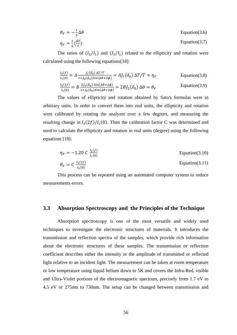
56
Equation(3.6)
Equation(3.7)
The ratios of and related to the ellipticity and rotation were
calculated using the following equations[18]:
Equation(3.8)
Equation(3.9)
The values of ellipticity and rotation obtained by Sato's formulas were in
arbitrary units. In order to convert them into real units, the ellipticity and rotation
were calibrated by rotating the analyzer over a few degrees, and measuring the
resulting change in . Then the calibration factor C was determined and
used to calculate the ellipticity and rotation in real units (degree) using the following
equations [18]:
Equation(3.10)
Equation(3.11)
This process can be repeated using an automated computer system to reduce
measurements errors.
3.3 Absorption Spectroscopy and the Principles of the Technique
Absorption spectroscopy is one of the most versatile and widely used
techniques to investigate the electronic structures of materials. It introduces the
transmission and reflection spectra of the samples, which provide rich information
about the electronic structures of these samples. The transmission or reflection
coefficient describes either the intensity or the amplitude of transmitted or reflected
light relative to an incident light. The measurement can be taken at room temperature
or low temperature using liquid helium down to 5K and covers the Infra-Red, visible
and Ultra-Violet portions of the electromagnetic spectrum, precisely from 1.7 eV to
4.5 eV or 275nm to 730nm. The setup can be changed between transmission and
57
reflection measurement geometry by detecting the reflected light rather than the
transmitted light, as shown in Fig.3.3.
Mo
no
ch
rom
ato
r
25
0W
Tu
ng
ste
n
ha
log
en
la
mp
Filter
Beam
splitterP
MT
PMT
Sample
PM
T
Lock-in
amplifier 1
Lock-in
amplifier 2
Signal
conditioning
unit & amplifier
AC
Optical
Chopper 1
Optical
Chopper 2
DC
I r
I1
I2
I0
Figure 3.3: An illustration of the absorption spectroscopy system used to measure the optical properties
of the samples discussed in this thesis.
A tungsten lamp with a power of 250 Watts was used to cover the desired
range of spectra. The light produced passes through a Spectro-275 spectrometer to
produce monochromatic light at the required wavelength. The monochromatic light is
filtered using a bandpass filter and splits in two beams of light with intensities of 50-
50 using a beam splitter device. One of these beams, called the reference beam, passes
through an optical chopper with a frequency of 370 MHZ before it is detected by a
reference photomultiplier tube detector (PMT). The photomultiplier tube (PMT)
detector converts the light intensity to an electrical signal before it is sent to the signal
conditioning unit. The other beam passes through another optical chopper with a
frequency of 310 MHZ. Then, it is transmitted through or reflected from the sample
based on the running measurement. The transmitted or reflected light is detected by
another photomultiplier tube detector. The PMT also sends the electrical signal to the
signal conditioning unit. The signal conditioning unit amplifies the signal and then
splits it into the AC and DC components. In this study, two Signal Recovery lock-in
amplifiers were used to record the AC measurements for the reference beam and the
transmitted or reflected light beam. Mirrors and lenses were used to focus the light
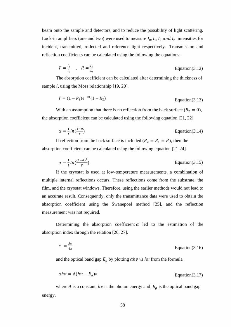
58
beam onto the sample and detectors, and to reduce the possibility of light scattering.
Lock-in amplifiers (one and two) were used to measure intensities for
incident, transmitted, reflected and reference light respectively. Transmission and
reflection coefficients can be calculated using the following the equations.
,
Equation(3.12)
The absorption coefficient can be calculated after determining the thickness of
sample , using the Moss relationship [19, 20].
Equation(3.13)
With an assumption that there is no reflection from the back surface ( ,
the absorption coefficient can be calculated using the following equation [21, 22]
Equation(3.14)
If reflection from the back surface is included ( , then the
absorption coefficient can be calculated using the following equation [21-24].
Equation(3.15)
If the cryostat is used at low-temperature measurements, a combination of
multiple internal reflections occurs. These reflections come from the substrate, the
film, and the cryostat windows. Therefore, using the earlier methods would not lead to
an accurate result. Consequently, only the transmittance data were used to obtain the
absorption coefficient using the Swanepoel method [25], and the reflection
measurement was not required.
Determining the absorption coefficient led to the estimation of the
absorption index through the relation [26, 27].
Equation(3.16)
and the optical band gap by plotting vs from the formula
Equation(3.17)
where A is a constant, is the photon energy and is the optical band gap
energy.
59
2.0 2.5 3.0 3.5 4.0 4.5 5.0
0
5
10
15
20
(h)(
eV/c
m)2
Energy (eV)
Eg
Figure 3.4: Tauc plot method used to estimate the optical band gap energy of semiconductors.
The intersection on the axis from the plot of versus in the linear
region in Fig.3.4 gives the optical band gap energy [20]. This method is known as
the Tauc plot [28] and has been used successfully by others [29-33].
3.4 Developments of Magneto-Optics and Absorption Systems
The magneto-optics and the absorption systems were put together by Dr Neal
of the University of Sheffield, with Prof. Kucera of Charles University [17]. Both
systems have been improved over the years by Anthony Behan and David Score.
Their steps were followed in order to add further enhancements to these systems.
The Magneto-optics system and the absorption system are greatly improved
when more optical pieces are supplemented to both systems in order to improve the
resolution and accuracy of the measurements and to handle low temperature
measurement. Instead of filters being changed manually during the measurement,
filters were automated and integrated within the setup software. Filters drivers were
programmed from scratch using the C++ command and Microsoft.Net framework and
fitted within the LabView program. The LabView program was used to manage both
systems, control the measurements, and acquire data. The Magneto-optic system
LabView program was upgraded. Consequently, most of the equipment’s old
LabView drivers failed to perform with the new version of the software. Therefore,
the equipment’s LabView drivers were reprogrammed to be compatible with the new

60
version. Both the Magneto-optics LabView programs in the field and at remanence
were reprogrammed and combined in one LabView Magneto-optics program. Fig.3.5
show the transmittance data measured using the absorption system before and after
the improvement for the same sample.
2.0 2.5 3.0 3.5 4.0 4.50.0
0.2
0.4
0.6
0.8
1.0
Tra
nsm
itta
nce
Energy (eV)
50T16SP 300K
(a)
2.0 2.5 3.0 3.5 4.0 4.50.0
0.2
0.4
0.6
0.8
1.0
50T16SP 300K
Tra
nsm
itta
nce
Energy (eV)
(b)
Figure 3.5: Transmittance a) before, and after b) improvement.
Changing the filter position manually created cut off points around 2.2 eV and
3.4 eV, as shown in Fig.5. After improvement, Fig.6 shows no cut off points and the
interference oscillation between the film and the substrate appears. This oscillation
could not be seen clearly before the improvement.
3.5 Systems Automation Method
There are several steps must be followed to acquire data using an instrument:
1. Install Software and Drivers.
2. Connect, Set Up, and configure Hardware.
3. Learn LabVIEW Basics.
4. Begin Your Application.
3.5.1 Install Software and Drivers
The first step to acquire data is to choose the right hardware platforms, and
then install the proper software and drivers for your application. There are several
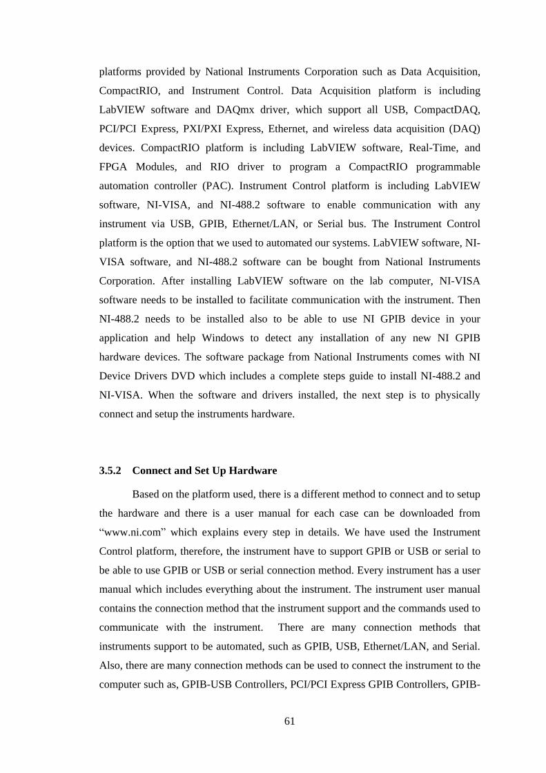
61
platforms provided by National Instruments Corporation such as Data Acquisition,
CompactRIO, and Instrument Control. Data Acquisition platform is including
LabVIEW software and DAQmx driver, which support all USB, CompactDAQ,
PCI/PCI Express, PXI/PXI Express, Ethernet, and wireless data acquisition (DAQ)
devices. CompactRIO platform is including LabVIEW software, Real-Time, and
FPGA Modules, and RIO driver to program a CompactRIO programmable
automation controller (PAC). Instrument Control platform is including LabVIEW
software, NI-VISA, and NI-488.2 software to enable communication with any
instrument via USB, GPIB, Ethernet/LAN, or Serial bus. The Instrument Control
platform is the option that we used to automated our systems. LabVIEW software, NI-
VISA software, and NI-488.2 software can be bought from National Instruments
Corporation. After installing LabVIEW software on the lab computer, NI-VISA
software needs to be installed to facilitate communication with the instrument. Then
NI-488.2 needs to be installed also to be able to use NI GPIB device in your
application and help Windows to detect any installation of any new NI GPIB
hardware devices. The software package from National Instruments comes with NI
Device Drivers DVD which includes a complete steps guide to install NI-488.2 and
NI-VISA. When the software and drivers installed, the next step is to physically
connect and setup the instruments hardware.
3.5.2 Connect and Set Up Hardware
Based on the platform used, there is a different method to connect and to setup
the hardware and there is a user manual for each case can be downloaded from
“www.ni.com” which explains every step in details. We have used the Instrument
Control platform, therefore, the instrument have to support GPIB or USB or serial to
be able to use GPIB or USB or serial connection method. Every instrument has a user
manual which includes everything about the instrument. The instrument user manual
contains the connection method that the instrument support and the commands used to
communicate with the instrument. There are many connection methods that
instruments support to be automated, such as GPIB, USB, Ethernet/LAN, and Serial.
Also, there are many connection methods can be used to connect the instrument to the
computer such as, GPIB-USB Controllers, PCI/PCI Express GPIB Controllers, GPIB-
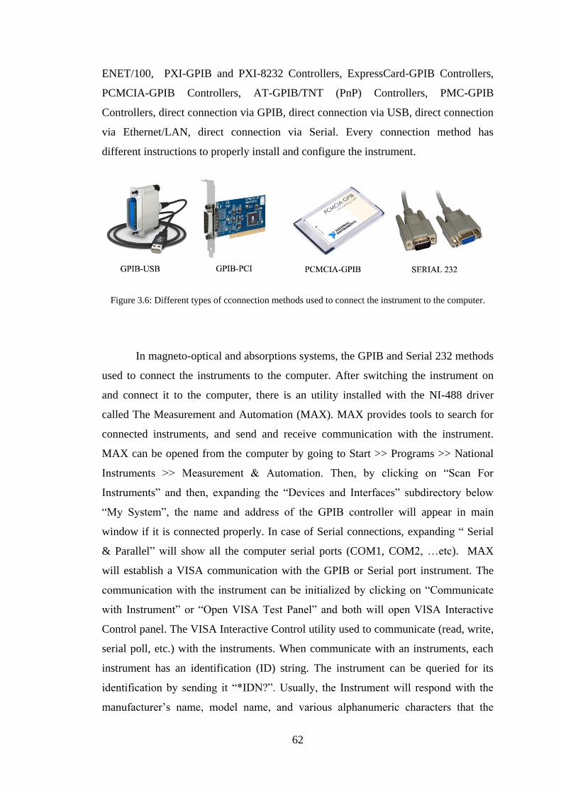
62
ENET/100, PXI-GPIB and PXI-8232 Controllers, ExpressCard-GPIB Controllers,
PCMCIA-GPIB Controllers, AT-GPIB/TNT (PnP) Controllers, PMC-GPIB
Controllers, direct connection via GPIB, direct connection via USB, direct connection
via Ethernet/LAN, direct connection via Serial. Every connection method has
different instructions to properly install and configure the instrument.
Figure 3.6: Different types of cconnection methods used to connect the instrument to the computer.
In magneto-optical and absorptions systems, the GPIB and Serial 232 methods
used to connect the instruments to the computer. After switching the instrument on
and connect it to the computer, there is an utility installed with the NI-488 driver
called The Measurement and Automation (MAX). MAX provides tools to search for
connected instruments, and send and receive communication with the instrument.
MAX can be opened from the computer by going to Start >> Programs >> National
Instruments >> Measurement & Automation. Then, by clicking on “Scan For
Instruments” and then, expanding the “Devices and Interfaces” subdirectory below
“My System”, the name and address of the GPIB controller will appear in main
window if it is connected properly. In case of Serial connections, expanding “ Serial
& Parallel” will show all the computer serial ports (COM1, COM2, …etc). MAX
will establish a VISA communication with the GPIB or Serial port instrument. The
communication with the instrument can be initialized by clicking on “Communicate
with Instrument” or “Open VISA Test Panel” and both will open VISA Interactive
Control panel. The VISA Interactive Control utility used to communicate (read, write,
serial poll, etc.) with the instruments. When communicate with an instruments, each
instrument has an identification (ID) string. The instrument can be queried for its
identification by sending it “*IDN?”. Usually, the Instrument will respond with the
manufacturer’s name, model name, and various alphanumeric characters that the

63
manufacturer uses to track firmware revision. At this point, transition from interactive
mode to programming mode using LabVIEW software is necessary.
Laboratory Virtual Instrumentation Engineering Workbench (LabVIEW) is a
system design platform and development environment for a visual programming
language to create and deploy measurement and control systems. LabVIEW works on
a variety of platforms including Microsoft Windows, Linux, UNIX, and Mac OS X. A
quick introduction about basic concepts of LabVIEW is essential to program software
to control, communicate and run the instruments using their commands.
3.6 Growth of In2O3 Thin Films
This section has been added to clarify the conditions associated with the
growth process, because most of the following chapters investigate the influence of
these growth conditions on the optical and magneto-optical properties of our doped
and un-doped In2O3 samples. I worked very closely with KACST engineers during the
installation of their new PLD system. All the growth conditions, such as oxygen
partial pressure, laser power, target and substrate separation, substrate temperature,
etc. were investigated in order to run the system correctly; the addition of this section
does not mean that I was involved in any of the growth processes. In fact, there is a
lack of structural data for our samples; therefore, we are facing difficulties in
comparing different samples sets.
The first step in producing a thin film is to make a target. The target consisted
of mixed amounts of In2O3 and the desired dopant. The target was prepared by a
widely used standard ceramic technique [34], where the powder component’s mass is
calculated and weighed then mixed and ground using a pestle. The mixture is sintered
at the preferred temperature for some time to form the right oxide syntheses. The
process of grinding the composition and sintering it is usually repeated several times
in order to eliminate any impurity phases and un-reacted components and to deliver a
high quality thin film. Then, the composition is compressed in vacuum by a high-
pressure press to 25000 kPa on a copper disc. As a result, a high-density target is
formed with a 25 mm diameter and 5 mm thickness. This method helps to reduce the
problem of particulate contamination of laser-deposited films [35]. The target is
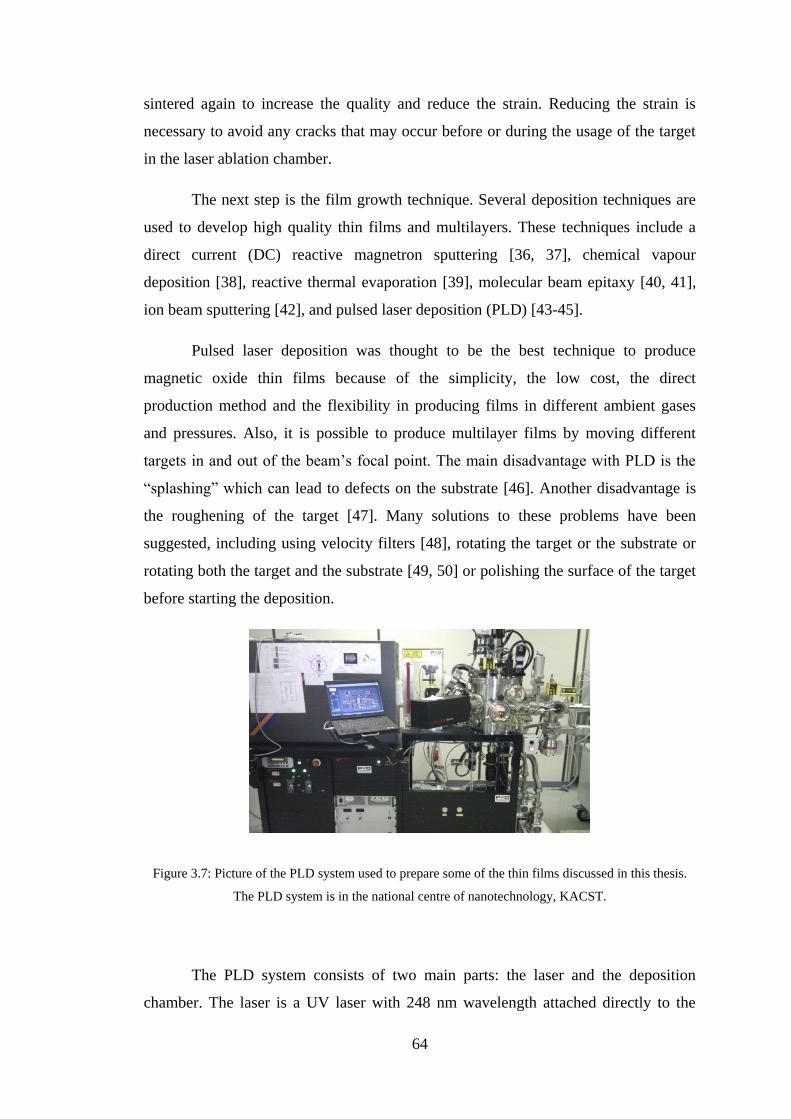
64
sintered again to increase the quality and reduce the strain. Reducing the strain is
necessary to avoid any cracks that may occur before or during the usage of the target
in the laser ablation chamber.
The next step is the film growth technique. Several deposition techniques are
used to develop high quality thin films and multilayers. These techniques include a
direct current (DC) reactive magnetron sputtering [36, 37], chemical vapour
deposition [38], reactive thermal evaporation [39], molecular beam epitaxy [40, 41],
ion beam sputtering [42], and pulsed laser deposition (PLD) [43-45].
Pulsed laser deposition was thought to be the best technique to produce
magnetic oxide thin films because of the simplicity, the low cost, the direct
production method and the flexibility in producing films in different ambient gases
and pressures. Also, it is possible to produce multilayer films by moving different
targets in and out of the beam’s focal point. The main disadvantage with PLD is the
“splashing” which can lead to defects on the substrate [46]. Another disadvantage is
the roughening of the target [47]. Many solutions to these problems have been
suggested, including using velocity filters [48], rotating the target or the substrate or
rotating both the target and the substrate [49, 50] or polishing the surface of the target
before starting the deposition.
Figure 3.7: Picture of the PLD system used to prepare some of the thin films discussed in this thesis.
The PLD system is in the national centre of nanotechnology, KACST.
The PLD system consists of two main parts: the laser and the deposition
chamber. The laser is a UV laser with 248 nm wavelength attached directly to the
65
chamber, as shown in Fig.3.8 with its beam focused directly at the surface of the
target. The laser pulse repetition rate is 10Hz with energy of 250 mJ per pulse. The
deposition chamber is a stainless-steel high vacuum compartment containing the
target and the substrate holders. The substrate holder can be heated to the desired
temperature and kept constant during ablation. The target holder can hold up to six
targets at the same time and rotate them during the ablation process using an electric
motor. This is particularly useful for the multilayer deposition process.
The substrate was cleaned with ethanol, clamped onto the substrate holder,
and maintained at the desired temperature during the ablation process. The substrate
temperature during the ablation process has a strong influence on the structural,
optical and electrical properties of the thin film. Thus, the substrate temperature may
vary. A high substrate temperature leads the transition metal ions to form isolated
clusters [51, 52].
Before the ablation starts, the deposition chamber is closed and pumped down
to the desired pressure. The oxygen pressure can be controlled by evacuating the
chamber to a minimum base pressure of 10-8
Torr. Then, through a controlled gas-
valve, oxygen, nitrogen and helium can be introduced into the chamber.
Figure 3.8: The plasma plume during the deposition where the substrate was clamped onto
the holder above the target, KACST.
When the target starts to rotate, it is pulsed by the laser beam. The target
surface absorbs the beam. Molecules, ions, atoms, and electrons evaporate in the form
of a plasma plume and are deposited on the surface of the substrate to achieve the
desired thin film.

66
When the deposition process is finished, the film and substrate are cooled
down to room temperature before they are released from the substrate holder. For this
study, the produced film was designed with free areas in every corner of the substrate.
These areas were used as a reference when measuring the film’s thickness using the
Dektak surface profiler. Then, the produced thin film named with a dissimilar name in
order to distinguish it among the other thin films and its specifications and growth
conditions written down and linked to its name as shown in Table. 3.1.
SAMPLE
Name
CO
NT
EN
T
TIM
E
(Min
)
d (
nm
)
T &
S s
ep.
(mm
)
S.T
EM
P.
(˚C
)
PR
ES
S.
mT
orr
LA
SE
R.E
(mJ)
DE
PO
SIT
ION
ME
TH
OD
An
nea
lin
g
for
30
min
SU
BS
TR
A
TE
489T71SP 35 156 32 600 2x10⁻³ -
Al 2
O3(0
00
1)
490T71SP
In2O3/
(5% NiO)
34 153 32 600 2x10⁻³
30
0
PL
D
500 C˚
491T71SP 34 141 32 600 2x10⁻³ 400 C˚
492T71SP 38 158 32 600 2x10⁻³ 300 C˚
Table 3.1: The method used to order to distinguish between the grown thin films.
.
Where the name of the samples 489T71SP, includes the sample number (489), the
target number (T71) and the substrate type (SP) which is sapphire. Time is pointed
to the deposition time, d is the thickness in nm unit, (T & S sep.) is the target and
the substrate separation distance in mm unit, (S.TEMP.) is the substrate
temperature, (PRESS.) is the pressure inside the chamber during the growth
process, (LASER.E) is the laser power used to prepare the thin film, and then, the
growth method which is PLD system in the case shown in table 3.1.
3.7 Suitable and Measurement of Thin Film Thickness
We investigated the influence of thickness on the optical and magneto-optical
properties of pure In2O3 thin films and found that for pure In2O3 thin films, the
suitable thicknesses are between 400nm to 500nm. For TM-doped In2O3 thin films,
the suitable thickness is around 200nm. This result was taken into account in all our
pure and TM-doped In2O3 thin films. However, there are two methods can be used to
determine the thickness of thin films. The first method is by fitting the transparent
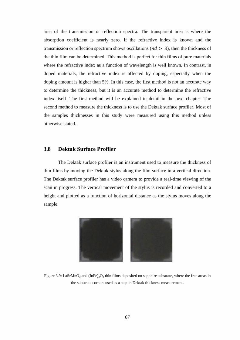
67
area of the transmission or reflection spectra. The transparent area is where the
absorption coefficient is nearly zero. If the refractive index is known and the
transmission or reflection spectrum shows oscillations ( ), then the thickness of
the thin film can be determined. This method is perfect for thin films of pure materials
where the refractive index as a function of wavelength is well known. In contrast, in
doped materials, the refractive index is affected by doping, especially when the
doping amount is higher than 5%. In this case, the first method is not an accurate way
to determine the thickness, but it is an accurate method to determine the refractive
index itself. The first method will be explained in detail in the next chapter. The
second method to measure the thickness is to use the Dektak surface profiler. Most of
the samples thicknesses in this study were measured using this method unless
otherwise stated.
3.8 Dektak Surface Profiler
The Dektak surface profiler is an instrument used to measure the thickness of
thin films by moving the Dektak stylus along the film surface in a vertical direction.
The Dektak surface profiler has a video camera to provide a real-time viewing of the
scan in progress. The vertical movement of the stylus is recorded and converted to a
height and plotted as a function of horizontal distance as the stylus moves along the
sample.
Figure 3.9: LaSrMnO3 and (InFe)2O3 thin films deposited on sapphire substrate, where the free areas in
the substrate corners used as a step in Dektak thickness measurement.
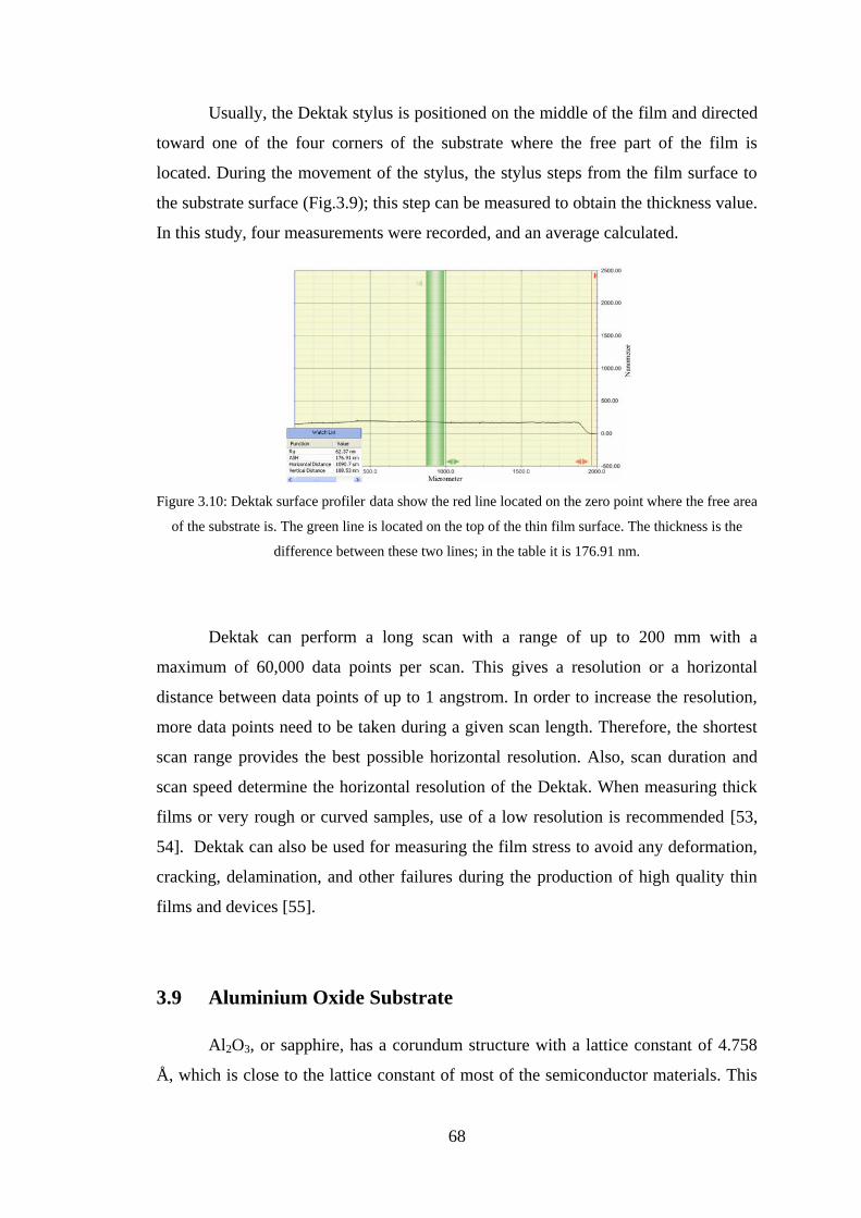
68
Usually, the Dektak stylus is positioned on the middle of the film and directed
toward one of the four corners of the substrate where the free part of the film is
located. During the movement of the stylus, the stylus steps from the film surface to
the substrate surface (Fig.3.9); this step can be measured to obtain the thickness value.
In this study, four measurements were recorded, and an average calculated.
Figure 3.10: Dektak surface profiler data show the red line located on the zero point where the free area
of the substrate is. The green line is located on the top of the thin film surface. The thickness is the
difference between these two lines; in the table it is 176.91 nm.
Dektak can perform a long scan with a range of up to 200 mm with a
maximum of 60,000 data points per scan. This gives a resolution or a horizontal
distance between data points of up to 1 angstrom. In order to increase the resolution,
more data points need to be taken during a given scan length. Therefore, the shortest
scan range provides the best possible horizontal resolution. Also, scan duration and
scan speed determine the horizontal resolution of the Dektak. When measuring thick
films or very rough or curved samples, use of a low resolution is recommended [53,
54]. Dektak can also be used for measuring the film stress to avoid any deformation,
cracking, delamination, and other failures during the production of high quality thin
films and devices [55].
3.9 Aluminium Oxide Substrate
Al2O3, or sapphire, has a corundum structure with a lattice constant of 4.758
Å, which is close to the lattice constant of most of the semiconductor materials. This
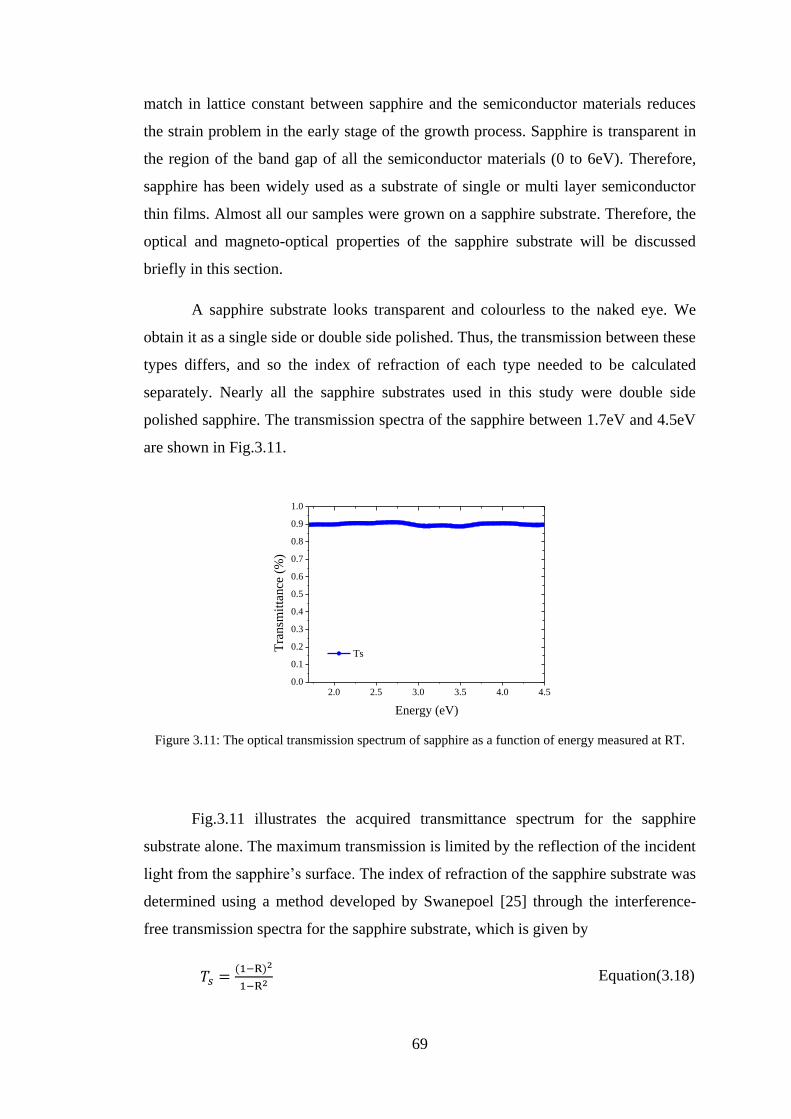
69
match in lattice constant between sapphire and the semiconductor materials reduces
the strain problem in the early stage of the growth process. Sapphire is transparent in
the region of the band gap of all the semiconductor materials (0 to 6eV). Therefore,
sapphire has been widely used as a substrate of single or multi layer semiconductor
thin films. Almost all our samples were grown on a sapphire substrate. Therefore, the
optical and magneto-optical properties of the sapphire substrate will be discussed
briefly in this section.
A sapphire substrate looks transparent and colourless to the naked eye. We
obtain it as a single side or double side polished. Thus, the transmission between these
types differs, and so the index of refraction of each type needed to be calculated
separately. Nearly all the sapphire substrates used in this study were double side
polished sapphire. The transmission spectra of the sapphire between 1.7eV and 4.5eV
are shown in Fig.3.11.
2.0 2.5 3.0 3.5 4.0 4.50.0
0.1
0.2
0.3
0.4
0.5
0.6
0.7
0.8
0.9
1.0
Tra
nsm
itta
nce
(%
)
Energy (eV)
Ts
Figure 3.11: The optical transmission spectrum of sapphire as a function of energy measured at RT.
Fig.3.11 illustrates the acquired transmittance spectrum for the sapphire
substrate alone. The maximum transmission is limited by the reflection of the incident
light from the sapphire’s surface. The index of refraction of the sapphire substrate was
determined using a method developed by Swanepoel [25] through the interference-
free transmission spectra for the sapphire substrate, which is given by
Equation(3.18)
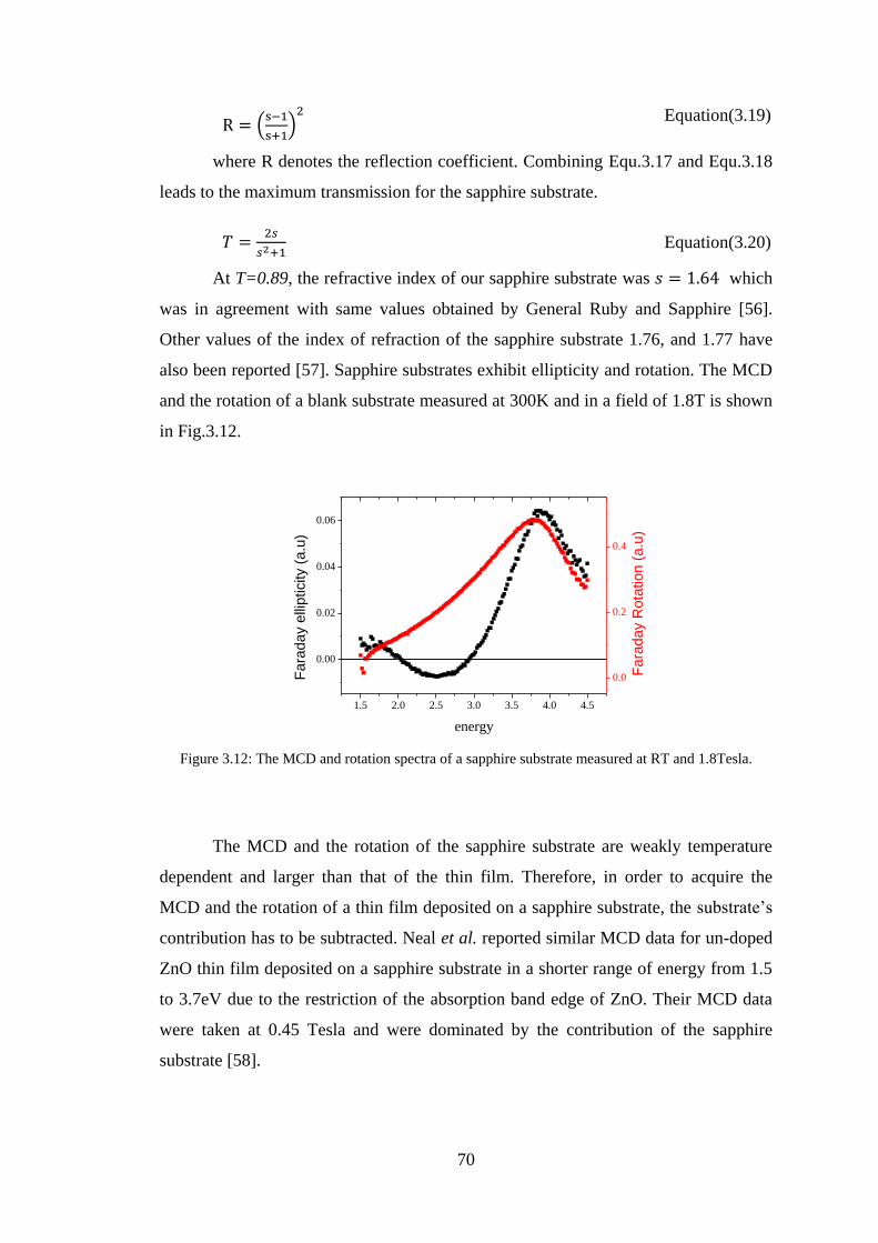
70
(
)
Equation(3.19)
where R denotes the reflection coefficient. Combining Equ.3.17 and Equ.3.18
leads to the maximum transmission for the sapphire substrate.
Equation(3.20)
At T=0.89, the refractive index of our sapphire substrate was which
was in agreement with same values obtained by General Ruby and Sapphire [56].
Other values of the index of refraction of the sapphire substrate 1.76, and 1.77 have
also been reported [57]. Sapphire substrates exhibit ellipticity and rotation. The MCD
and the rotation of a blank substrate measured at 300K and in a field of 1.8T is shown
in Fig.3.12.
1.5 2.0 2.5 3.0 3.5 4.0 4.5
0.00
0.02
0.04
0.06
energy
Fara
da
y e
llipticity (
a.u
)
0.0
0.2
0.4
Fara
da
y R
ota
tion (
a.u
)
Figure 3.12: The MCD and rotation spectra of a sapphire substrate measured at RT and 1.8Tesla.
The MCD and the rotation of the sapphire substrate are weakly temperature
dependent and larger than that of the thin film. Therefore, in order to acquire the
MCD and the rotation of a thin film deposited on a sapphire substrate, the substrate’s
contribution has to be subtracted. Neal et al. reported similar MCD data for un-doped
ZnO thin film deposited on a sapphire substrate in a shorter range of energy from 1.5
to 3.7eV due to the restriction of the absorption band edge of ZnO. Their MCD data
were taken at 0.45 Tesla and were dominated by the contribution of the sapphire
substrate [58].
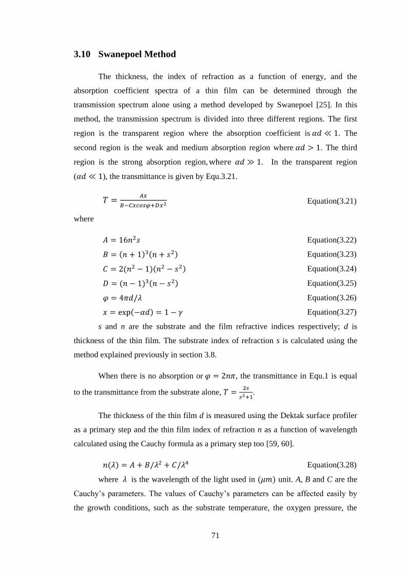
71
3.10 Swanepoel Method
The thickness, the index of refraction as a function of energy, and the
absorption coefficient spectra of a thin film can be determined through the
transmission spectrum alone using a method developed by Swanepoel [25]. In this
method, the transmission spectrum is divided into three different regions. The first
region is the transparent region where the absorption coefficient is . The
second region is the weak and medium absorption region where . The third
region is the strong absorption region . In the transparent region
( ), the transmittance is given by Equ.3.21.
Equation(3.21)
where
Equation(3.22)
Equation(3.23)
Equation(3.24)
Equation(3.25)
Equation(3.26)
Equation(3.27)
s and n are the substrate and the film refractive indices respectively; d is
thickness of the thin film. The substrate index of refraction s is calculated using the
method explained previously in section 3.8.
When there is no absorption or , the transmittance in Equ.1 is equal
to the transmittance from the substrate alone,
.
The thickness of the thin film d is measured using the Dektak surface profiler
as a primary step and the thin film index of refraction n as a function of wavelength
calculated using the Cauchy formula as a primary step too [59, 60].
Equation(3.28)
where is the wavelength of the light used in unit. A, B and C are the
Cauchy’s parameters. The values of Cauchy’s parameters can be affected easily by
the growth conditions, such as the substrate temperature, the oxygen pressure, the
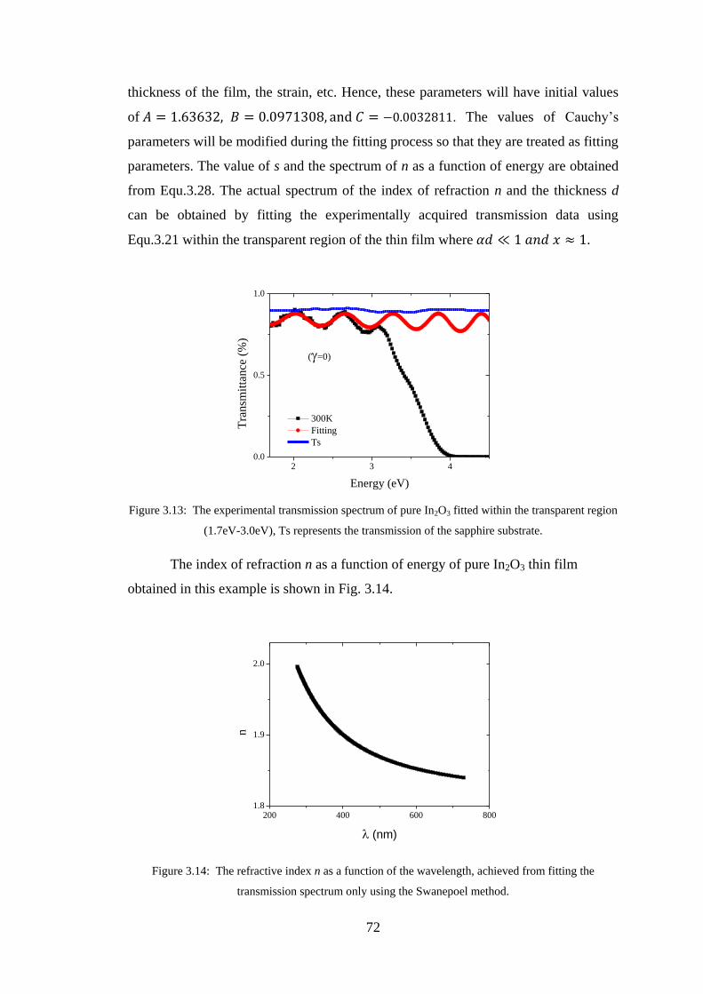
72
thickness of the film, the strain, etc. Hence, these parameters will have initial values
of . The values of Cauchy’s
parameters will be modified during the fitting process so that they are treated as fitting
parameters. The value of s and the spectrum of n as a function of energy are obtained
from Equ.3.28. The actual spectrum of the index of refraction n and the thickness d
can be obtained by fitting the experimentally acquired transmission data using
Equ.3.21 within the transparent region of the thin film where .
2 3 40.0
0.5
1.0
Tra
nsm
itta
nce
(%
)
Energy (eV)
300K
Fitting
Ts
(=0)
Figure 3.13: The experimental transmission spectrum of pure In2O3 fitted within the transparent region
(1.7eV-3.0eV), Ts represents the transmission of the sapphire substrate.
The index of refraction n as a function of energy of pure In2O3 thin film
obtained in this example is shown in Fig. 3.14.
200 400 600 8001.8
1.9
2.0
n
(nm)
Figure 3.14: The refractive index n as a function of the wavelength, achieved from fitting the
transmission spectrum only using the Swanepoel method.
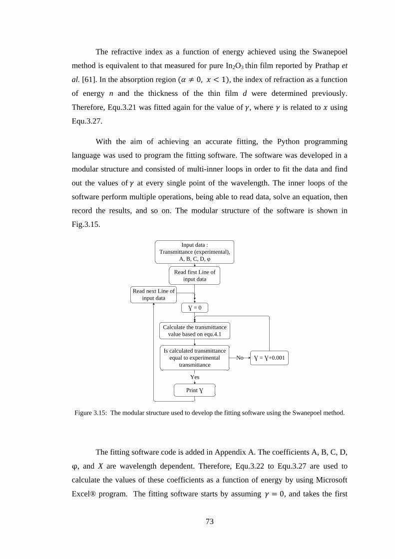
73
The refractive index as a function of energy achieved using the Swanepoel
method is equivalent to that measured for pure In2O3 thin film reported by Prathap et
al. [61]. In the absorption region , the index of refraction as a function
of energy n and the thickness of the thin film d were determined previously.
Therefore, Equ.3.21 was fitted again for the value of , where is related to using
Equ.3.27.
With the aim of achieving an accurate fitting, the Python programming
language was used to program the fitting software. The software was developed in a
modular structure and consisted of multi-inner loops in order to fit the data and find
out the values of at every single point of the wavelength. The inner loops of the
software perform multiple operations, being able to read data, solve an equation, then
record the results, and so on. The modular structure of the software is shown in
Fig.3.15.
Input data :
Transmittance (experimental),
A, B, C, D, φ
Read first Line of
input data
Calculate the transmittance
value based on equ.4.1
Is calculated transmittance
equal to experimental
transmittance
Ɣ = 0
Print Ɣ
Yes
Read next Line of
input data
Ɣ = Ɣ+0.001No
Figure 3.15: The modular structure used to develop the fitting software using the Swanepoel method.
The fitting software code is added in Appendix A. The coefficients A, B, C, D,
, and X are wavelength dependent. Therefore, Equ.3.22 to Equ.3.27 are used to
calculate the values of these coefficients as a function of energy by using Microsoft
Excel® program. The fitting software starts by assuming , and takes the first
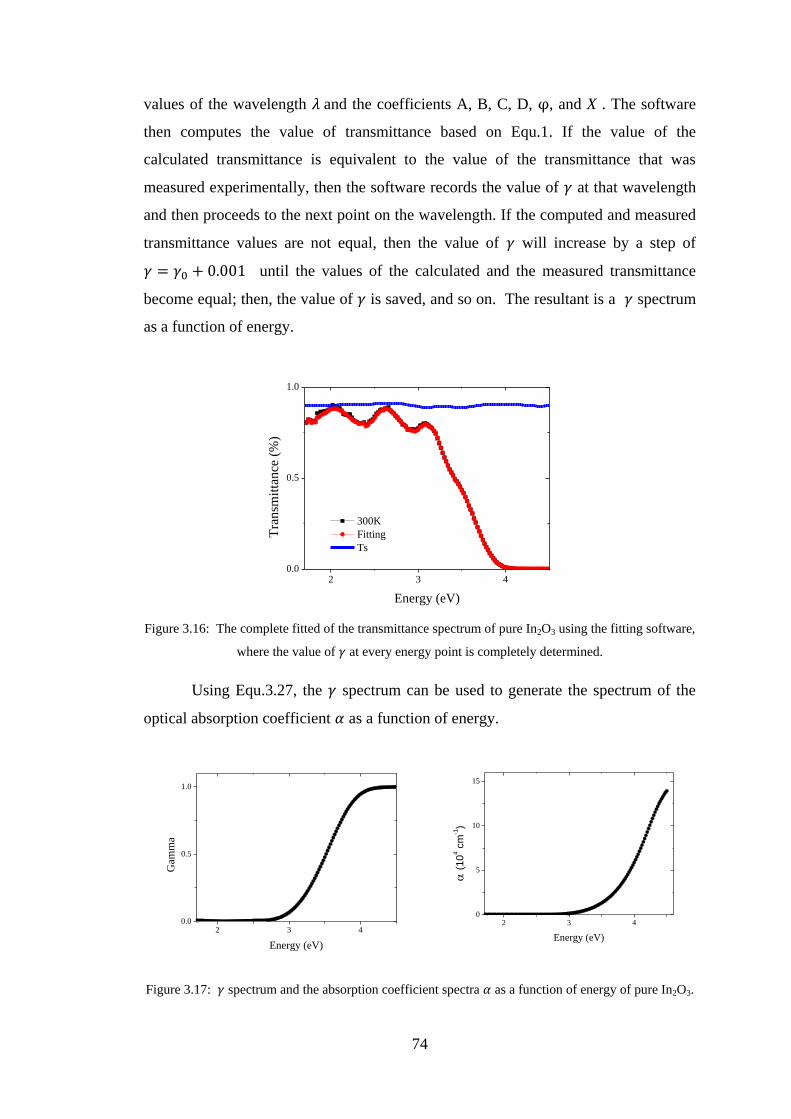
74
values of the wavelength and the coefficients A, B, C, D, , and X . The software
then computes the value of transmittance based on Equ.1. If the value of the
calculated transmittance is equivalent to the value of the transmittance that was
measured experimentally, then the software records the value of at that wavelength
and then proceeds to the next point on the wavelength. If the computed and measured
transmittance values are not equal, then the value of will increase by a step of
until the values of the calculated and the measured transmittance
become equal; then, the value of is saved, and so on. The resultant is a spectrum
as a function of energy.
2 3 40.0
0.5
1.0
Tra
nsm
itta
nce
(%
)
Energy (eV)
300K
Fitting
Ts
Figure 3.16: The complete fitted of the transmittance spectrum of pure In2O3 using the fitting software,
where the value of at every energy point is completely determined.
Using Equ.3.27, the spectrum can be used to generate the spectrum of the
optical absorption coefficient as a function of energy.
2 3 40.0
0.5
1.0
Gam
ma
Energy (eV)
2 3 40
5
10
15
(
10
4 c
m-1)
Energy (eV)
Figure 3.17: spectrum and the absorption coefficient spectra as a function of energy of pure In2O3.

75
Obtaining the absorption coefficient spectra as a function of energy paves
the way to determining the optical band gap of the system using a Tauc plot [28], as
explained previously in section 3.3. This method is very accurate in determining the
optical absorption coefficient spectrum where it is not affected by any changes in the
fitting parameters, such as the thickness and the index of refraction. The Swanepoel
method is used in the following chapters to deal with any transmission data taken at
low temperature; otherwise, Equ.3.15 is used and the reflection spectrum is
considered.
76
3.11 References
1. K. SATO, Jpn. J. Appl. Phys. 20, 2403-2409 (1981).
2. K. Ohgushi, Y. Okimoto, T. Ogasawara, S. Miyasaka and Y. Tokura, J. Phys.
Soc. Jpn. 77, (2008).
3. T. Ishibashi, Z. Kuang, S. Yufune, T. Kawata, M. Oda, T. Tani, Y. Iimura, K.
Sato, Y. Konishi, K. Akahane, X. Zhao and T. Hasegawa, J. Appl. Phys. 100,
(2006).
4. P. T. Chiu, and B. W. Wessels, Appl. Phys. Lett. 89, (2006).
5. H. L. Liu, K. S. Lu, M. X. Kuo, L. Uba, S. Uba, L.M. Wang and H. T. Jeng, J.
Appl. Phys. 99, (2006).
6. K. Ohgushi, T. Ogasawara, Y. Okimoto, S. Miyasaka and Y. Tokura, Phys.
Rev. B 72, (2005).
7. D. A. Smith, Y. A. Barnakov, B. L. Scott, S. A. White and K. L. Stokes.
Magneto-optical spectra of closely spaced magnetite nanoparticles. in 49th
Annual Conference on Magnetism and Magnetic Materials. 2004.
Jacksonville, FL.
8. K. J. Kim, J. H. Lee and S. H. Lee, J. Magn. Magn. Mater. 279, 173-177
(2004).
9. D. A. Allwood, G. Xiong, M. D. Cooke and R. P. Cowburn, J. Phys. D-Appl.
Phys. 36, 2175-2182 (2003).
10. G. P. Moore, J. Ferre, A. Mougin, M. Moreno and L. Daweritz, J. Appl. Phys.
94, 4530-4534 (2003).
11. K. J. Kim, H. S. Lee, M. H. Lee and S. H. Lee, J. Appl. Phys. 91, 9974-9977
(2002).
12. S. Lee, S. Park and C.M. Falco. Magnetic properties of ultra-thin MBE-grown
multilayers. in 4th International Symposium on Metallic Multilayers. 2001.
Aachen, Germany.
13. K. J. Kim, S. J. Lee, T. A. Wiener and D. W. Lynch, J. Appl. Phys. 89, 244-
248 (2001).
14. T.L. Cheeks, M. Brasil, T. Sands, J. P. Harbison, D. E. Aspnes, V. G.
Keramidas and S. J. Allen, Appl. Phys. Lett. 60, 1393-1395 (1992).
15. S. T. Purcell, M. T. Johnson, N. W. E. McGee, J. J. Devries, W. B. Zeper and
W. Hoving, J. Appl. Phys. 73, 1360-1367 (1993).

77
16. K. Sato, H. Hongu, H. Ikekame, Y. Tosaka, M. Watanabe, K. Takanashi and
H. Fujimori, Jpn. J. Appl. Phys. Part 1-Regular Papers Short Notes & Review
Papers 32, 989-995 (1993).
17. A. Behan, Characterisation of Doped ZnO Thin Films for Spintronic
Applications,2008, University of Sheffield.
18. W. P. Van Drent, and T. Suzuki, J. Magn. Magn. Mater. 175, 53-62 (1997).
19. M. Fox, Optical properties of solids. Oxford master series in condensed matter
physics 2001, Oxford ; New York: Oxford University Press. xii, 305 p.
20. N. G. Patel, and B. H. Lashkari, Journal of Materials Science 27, 3026-3031
(1992).
21. J. I. Pankove, Optical processes in semiconductors. Prentice-Hall electrical
engineering series Solid state physical electronics series 1971, Englewood
Cliffs, N.J.,: Prentice-Hall. xvii, 422 p.
22. A. A. Bahgat, M. M. El-Desoky, A. Al-Hajry, A. Al-Mogeeth and M. S. Al-
Assiri, Optics & Laser Technology 42, 994-1003 (2010).
23. B. Radha Krishna, T. K. Subramanyam, B. S. Naidu and S. Uthanna, Opt.
Mater. 15, 217-224 (2000).
24. C. Xu, C. Ouyang, R. Jia, Y. Li and X. Wang, J. Appl. Polym. Sci. 111, 1763-
1768 (2009).
25. R. Swanepoel, J. Phys. E: Scientific Instruments 16, 1214 (1983).
26. J. Sánchez-González, A. Díaz-Parralejo, A. L. Ortiz and F. Guiberteau, Appl.
Surf. Sci. 252, 6013-6017 (2006).
27. P. Dirk, and S. P. Frederic, J. Phys. D: Appl. Phys. 36, 1850 (2003).
28. J. Tauc, Amorphous and liquid semiconductors 1974, London, New York,:
Plenum. ix, 441 p.
29. Y. Ohhata, F. Shinoki and S. Yoshida, Thin Solid Films 59, 255-261 (1979).
30. M. J. Alam, and D. C. Cameron, Thin Solid Films 377-378, 455-459 (2000).
31. H. Han, J. W. Mayer and T. L. Alford, J. Appl. Phys. 100, 083715 (2006).
32. D. Beena, K. J. Lethy, R. Vinodkumar, V. P. M. Pillai, V. Ganesan, D. M.
Phase and S. K. Sudheer, Appl. Surf. Sci. 255, 8334-8342 (2009).
33. H. Han, J. W. Mayer and T. L. Alford, J. Appl. Phys. 99, 123711-123711-7
(2006).
34. G. H. Jonker, and J. H. V. Santen, Physica 16, 337-349 (1950).
78
35. J. F. Lawler, J. M. D. Coey, J. G. Lunney and V. Skumryev, J. Phys.:
Condensed Matter 8, 10737 (1996).
36. A. N. H. Al-Ajili, and S. C. Bayliss, Thin Solid Films 305, 116-123 (1997).
37. S. Kasiviswanathan, and G. Rangarajan, J. Appl. Phys. 75, 2572-2577 (1994).
38. S. Suh, and D. M. Hoffman, Journal of the American Chemical Society 122,
9396-9404 (2000).
39. C. A. Pan, and T. P. Ma, Appl. Phys. Lett. 37, 163-165 (1980).
40. C. H. Shih, I. Lo, W. Y. Pang and C. H. Hiseh, J. Phys. Chem. Solids 71,
1664-1668 (2010).
41. K. Umeno, Y. Furukawa, N. Urakami, R. Noma, S. Mitsuyoshi, A. Wakahara
and H. Yonezu, Physica E: Low-dimensional Systems and Nanostructures 42,
2772-2776 (2010).
42. J. S. Cho, K. H. Yoon and S. K. Koh, J. Appl. Phys. 89, 3223-3228 (2001).
43. E. J. Tarsa, J. H. English and J. S. Speck, Appl. Phys. Lett. 62, 2332-2334
(1993).
44. S. P. Sena, R. A. Lindley, H. J. Blythe, C. Sauer, M. Al-Kafarji and G. A.
Gehring, J. Magn. Magn. Mater. 176, 111-126 (1997).
45. W. Svendsen, J. Schou, B. Thestrup and O. Ellegaard, Appl. Surf. Sci. 96-98,
518-521 (1996).
46. D. B. Chrisey, and G. K. Hubler, Pulsed laser deposition of thin films 1994,
New York: J. Wiley. xxviii, 613 p.
47. E. van de Riet, U. K. P. Biermann and J. Dieleman, Thin Solid Films 241,
134-137 (1994).
48. D. Lubben, S. A. Barnett, K. Suzuki, S. Gorbatkin and J. E. Greene, Journal of
Vacuum Science & Technology B: Microelectronics and Nanometer
Structures 3, 968-974 (1985).
49. J. A. Greer, High quality YBCO films grown over large areas by pulsed laser
deposition. 1992. AVS.
50. S. R. Foltyn, R.E. Muenchausen, R. C. Dye, X. D. Wu, L. Luo, D. W. Cooke
and R. C. Taber, Appl. Phys. Lett. 59, 1374-1376 (1991).
51. P. Sharma, A. Gupta, K. V. Rao, F. J. Owens, R. Sharma, R. Ahuja, J. M. O.
Guillen, B. Johansson and G. A. Gehring, Nat Mater 2, 673-677 (2003).
79
52. A. K. Pradhan, K. Zhang, S. Mohanty, J. B. Dadson, D. Hunter, J. Zhang, D. J.
Sellmyer, U. N. Roy, Y. Cui, A. Burger, S. Mathews, B. Joseph, B. R. Sekhar
and B. K. Roul, Appl. Phys. Lett. 86, 152511 (2005).
53. nuance.northwestern. Available from:
http://www.nuance.northwestern.edu/media/keckii%20pdf/dektak.pdf.
54. Veeco. Available from: http://www.veeco.com/pdfs/datasheets/B509-RevA3-
Dektak_150+_Surface_Profiler-Brochure.pdf.
55. Rpi. Available from:
http://www.rpi.edu/dept/cie/mncr/documents/AN516_Dektak_Stress_Measure
.pdf.
56. G. R. S. Co, 2011; Available from:
http://www.generalruby.com/sapphire.html.
57. R. Reed, 1998; Available from:
http://hypertextbook.com/facts/2007/GaryChang.shtml.
58. J. R. Neal, A. J. Behan, R. M. Ibrahim, H. J. Blythe, M. Ziese, A. M. Fox and
G. A. Gehring, Phys. Rev. Lett.96, 197208 (2006).
59. B. P. Chandra, and S. C. Bhaiya, American J. Phys. 51, 160-161 (1983).
60. S. A. Khodier, Optics & Laser Technology 34, 125-128 (2002).
61. P. Prathap, Y. P. V. Subbaiah, M. Devika and K. T. R. Reddy, Materials
Chemistry and Physics 100, 375-379 (2006).
80
Chapter 4 – Pure In2O3
4.1 Introduction Variations in the oxygen partial pressure during the deposition process of thin
films affect not only the structure, but also the physical properties of these films.
Oxygen partial pressure has been found to be a key parameter in order to increase or
decrease the density of oxygen vacancies. The oxygen vacancies act as donors, which
leads to an increment in the carrier concentration. Variations in carrier concentration
have a major impact on most of the physical properties of the materials. Therefore, by
altering the oxygen partial pressure during the growth process, it is possible to archive
the desired structure, surface, interface, and many other physical properties of the
films while maintaining high-quality epitaxy. Understanding the variations in the
absorption and refractive index of an un-doped system with oxygen partial pressure is
an essential step towards understanding the behaviour of the MCD and rotation of that
system, and providing background knowledge for TM-doped systems. This chapter
investigates the behaviour of oxygen impurity bands formed within the band gap
energy of the host In2O3 in the absence of any effect originating from the TM 3d
impurity band and related transitions. This will help us to predict and understand the
impact of TM-doping and other growth conditions on In2O3 semiconductors. In
addition, this chapter introduces a study about the tin-doping dependence of the
optical and magneto-optical properties of pure In2O3. Tin doping affects the In2O3 thin
films because Sn4+ ions substitute In3+ ions and release an electron. Therefore, the
carrier density increases with tin doping. Variations in the carrier concentration have a
major impact on most of the physical properties. They can change the thin film from
an isolator to a metallic material through the semiconductor regime.
4.2 Experiment Details, Results, and Discussion In order to investigate the influence of oxygen partial pressure on the optical
properties of pure In2O3, ten thin films of pure In2O3 were prepared on sapphire
substrates at 550 ˚C using the PLD system with laser energy of 250 mJ. The oxygen
partial pressure within the growth chamber was varied between 20x10-3 mTorr and
100 mTorr. These thin films were obtained through collaboration with A. Alyamani’s
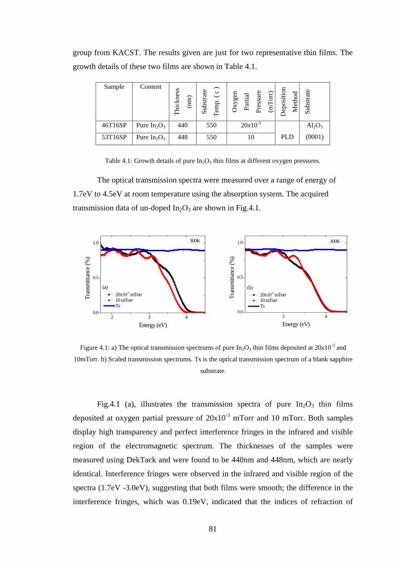
81
group from KACST. The results given are just for two representative thin films. The
growth details of these two films are shown in Table 4.1.
Sample Content
Thic
knes
s
(nm
)
Subs
trate
Tem
p. (
c )
Oxy
gen
Parti
al
Pres
sure
(mTo
rr)
Dep
ositi
on
Met
hod
Subs
trate
46T16SP Pure In2O3 440 550 20x10-3
PLD
Al2O3
(0001) 53T16SP Pure In2O3 448 550 10
Table 4.1: Growth details of pure In2O3 thin films at different oxygen pressures.
The optical transmission spectra were measured over a range of energy of
1.7eV to 4.5eV at room temperature using the absorption system. The acquired
transmission data of un-doped In2O3 are shown in Fig.4.1.
2 3 40.0
0.5
1.0
Tran
smitt
ance
(%)
Energy (eV)
20x10-3 mTorr 10 mTorr Ts
300K
(a)
3 40.0
0.5
1.0
Tr
ansm
ittan
ce (%
)
Energy (eV)
20x10-3 mTorr 10 mTorr Ts
300K
(b)
Figure 4.1: a) The optical transmission spectrums of pure In2O3 thin films deposited at 20x10-3 and
10mTorr. b) Scaled transmission spectrums. Ts is the optical transmission spectrum of a blank sapphire
substrate.
Fig.4.1 (a), illustrates the transmission spectra of pure In2O3 thin films
deposited at oxygen partial pressure of 20x10-3 mTorr and 10 mTorr. Both samples
display high transparency and perfect interference fringes in the infrared and visible
region of the electromagnetic spectrum. The thicknesses of the samples were
measured using DekTack and were found to be 440nm and 448nm, which are nearly
identical. Interference fringes were observed in the infrared and visible region of the
spectra (1.7eV -3.0eV), suggesting that both films were smooth; the difference in the
interference fringes, which was 0.19eV, indicated that the indices of refraction of
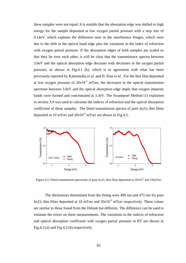
82
these samples were not equal. It is notable that the absorption edge was shifted to high
energy for the sample deposited at low oxygen partial pressure with a step size of
0.14eV, which explains the difference seen in the interference fringes, which were
due to the shift in the optical band edge plus the variations in the index of refraction
with oxygen partial pressure. If the absorption edges of both samples are scaled so
that they lie over each other, it will be clear that the transmittance spectra between
3.0eV and the optical absorption edge decrease with decreases in the oxygen partial
pressure, as shown in Fig.4.1 (b), which is in agreement with what has been
previously reported by Kaleemulla et al. and H. Kim et al. For the thin film deposited
at low oxygen pressure of 20x10-3 mTorr, the decreases in the optical transmission
spectrum between 3.0eV and the optical absorption edge imply that oxygen impurity
bands were formed and concentrated at 3.3eV. The Swanepoel Method [1] explained
in section 3.9 was used to calculate the indices of refraction and the optical absorption
coefficient of these samples. The fitted transmission spectra of pure In2O3 thin films
deposited at 10 mTorr and 20x10-3 mTorr are shown in Fig.4.2.
2 3 40.0
0.5
1.0
Tran
smitt
ance
(%)
Energy (eV)
300K Fitting2x10-3 mTorr
2 3 40.0
0.5
1.0
Tran
smitt
ance
(%)
Energy (eV)
300K Fitting10 mTorr
Figure 4.2: Fitted transmission spectrums of pure In2O3 thin films deposited at 20x10-3 and 10mTorr.
The thicknesses determined from the fitting were 496 nm and 475 nm for pure
In2O3 thin films deposited at 10 mTorr and 20x10-3 mTorr respectively. These values
are similar to those found from the Dektak but different. The difference can be used to
estimate the errors on these measurements. The variations in the indices of refraction
and optical absorption coefficient with oxygen partial pressure at RT are shown in
Fig.4.3 (a) and Fig.4.3 (b) respectively.
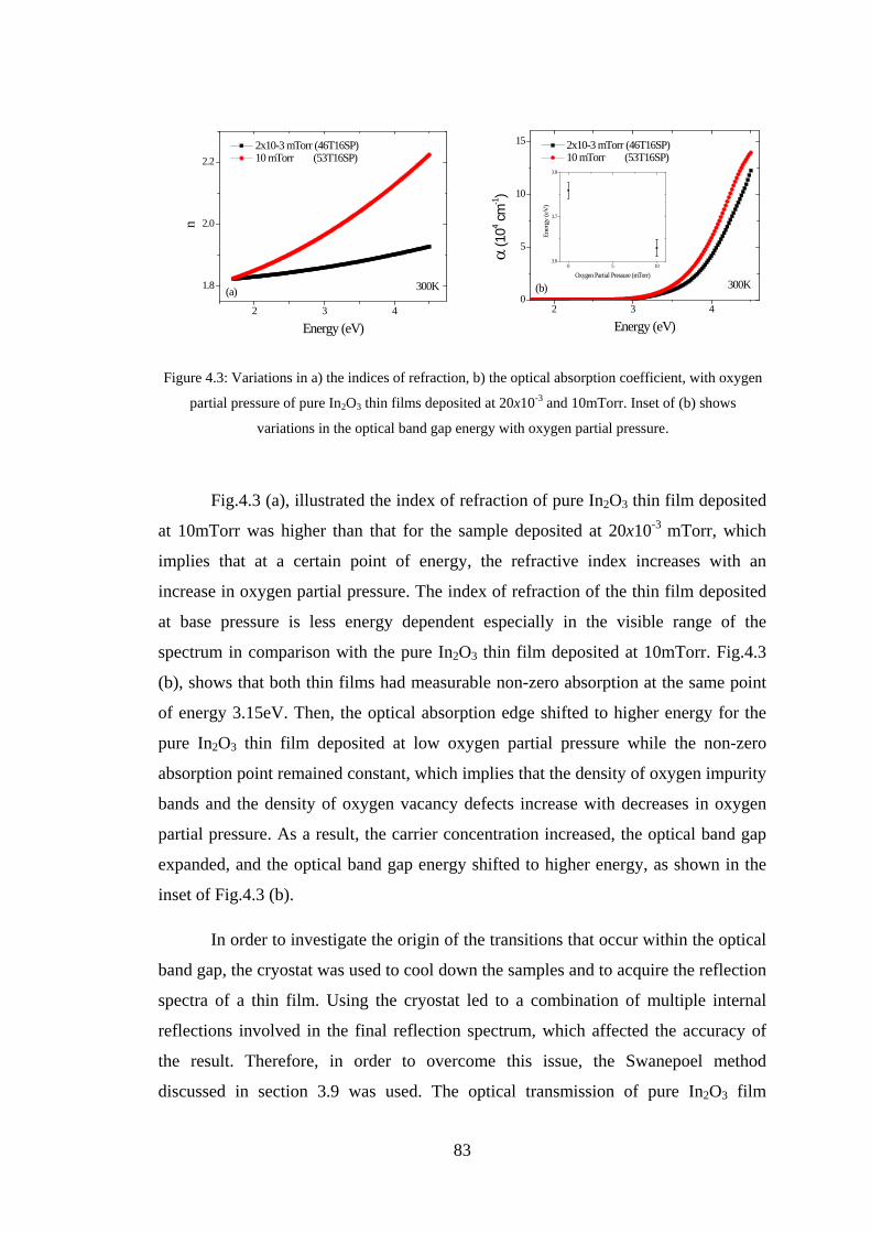
83
2 3 4
1.8
2.0
2.2
n
Energy (eV)
2x10⁻³ mTorr (46T16SP) 10 mTorr (53T16SP)
300K(a)
2 3 40
5
10
15
0 5 103.6
3.7
3.8
Ener
gy (e
V)
Oxygen Partial Pressure (mTorr)
α (1
04 cm
-1)
Energy (eV)
2x10⁻³ mTorr (46T16SP) 10 mTorr (53T16SP)
300K(b)
Figure 4.3: Variations in a) the indices of refraction, b) the optical absorption coefficient, with oxygen
partial pressure of pure In2O3 thin films deposited at 20x10-3 and 10mTorr. Inset of (b) shows
variations in the optical band gap energy with oxygen partial pressure.
Fig.4.3 (a), illustrated the index of refraction of pure In2O3 thin film deposited
at 10mTorr was higher than that for the sample deposited at 20x10-3 mTorr, which
implies that at a certain point of energy, the refractive index increases with an
increase in oxygen partial pressure. The index of refraction of the thin film deposited
at base pressure is less energy dependent especially in the visible range of the
spectrum in comparison with the pure In2O3 thin film deposited at 10mTorr. Fig.4.3
(b), shows that both thin films had measurable non-zero absorption at the same point
of energy 3.15eV. Then, the optical absorption edge shifted to higher energy for the
pure In2O3 thin film deposited at low oxygen partial pressure while the non-zero
absorption point remained constant, which implies that the density of oxygen impurity
bands and the density of oxygen vacancy defects increase with decreases in oxygen
partial pressure. As a result, the carrier concentration increased, the optical band gap
expanded, and the optical band gap energy shifted to higher energy, as shown in the
inset of Fig.4.3 (b).
In order to investigate the origin of the transitions that occur within the optical
band gap, the cryostat was used to cool down the samples and to acquire the reflection
spectra of a thin film. Using the cryostat led to a combination of multiple internal
reflections involved in the final reflection spectrum, which affected the accuracy of
the result. Therefore, in order to overcome this issue, the Swanepoel method
discussed in section 3.9 was used. The optical transmission of pure In2O3 film
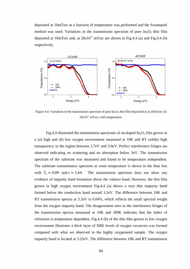
84
deposited at 10mTorr as a function of temperature was performed and the Swanepoel
method was used. Variations in the transmission spectrum of pure In2O3 thin film
deposited at 10mTorr and, at 20x10-3 mTorr are shown in Fig.4.4 (a) and Fig.4.4 (b)
respectively.
2 3 40.0
0.5
1.0
53T16SP
Tran
smitt
ance
(%)
Energy (eV)
10K 300K Ts
(a) 10 mTorr
2 3 40.0
0.5
1.0 (b) 20x10-3 mTorr
46T16SP
Tran
smitt
ance
(%)
Energy (eV)
10K 300K Ts
Figure 4.4: Variations in the transmission spectrum of pure In2O3 thin film deposited at a) 10mTorr, b)
20x10-3 mTorr, with temperature.
Fig.4.4 illustrated the transmission spectrums of un-doped In2O3 film grown in
a (a) high and (b) low oxygen environment measured at 10K and RT exhibit high
transparency in the region between 1.7eV and 3.0eV. Perfect interference fringes are
observed indicating no scattering and no absorption below 3eV. The transmission
spectrum of the substrate was measured and found to be temperature independent.
The substrate transmittance spectrum at room temperature is shown in the blue line
with 𝑇𝑠 = 0.89 and 𝑠 = 1.64. The transmission spectrum does not show any
evidence of impurity band formation above the valance band. However, the thin film
grown in high oxygen environment Fig.4.4 (a) shows a very thin impurity band
formed below the conduction band around 3.2eV. The difference between 10K and
RT transmission spectra at 3.2eV is 0.04%, which reflects the small spectral weight
from the oxygen impurity band. The disagreement seen in the interference fringes of
the transmission spectra measured at 10K and 300K indicates that the index of
refraction is temperature dependent. Fig.4.4 (b) of the thin film grown in low oxygen
environment illustrates a thick layer of NBE levels of oxygen vacancies was formed
compared with what we observed in the highly oxygenated sample. The oxygen
impurity band is located at 3.25eV. The difference between 10K and RT transmission
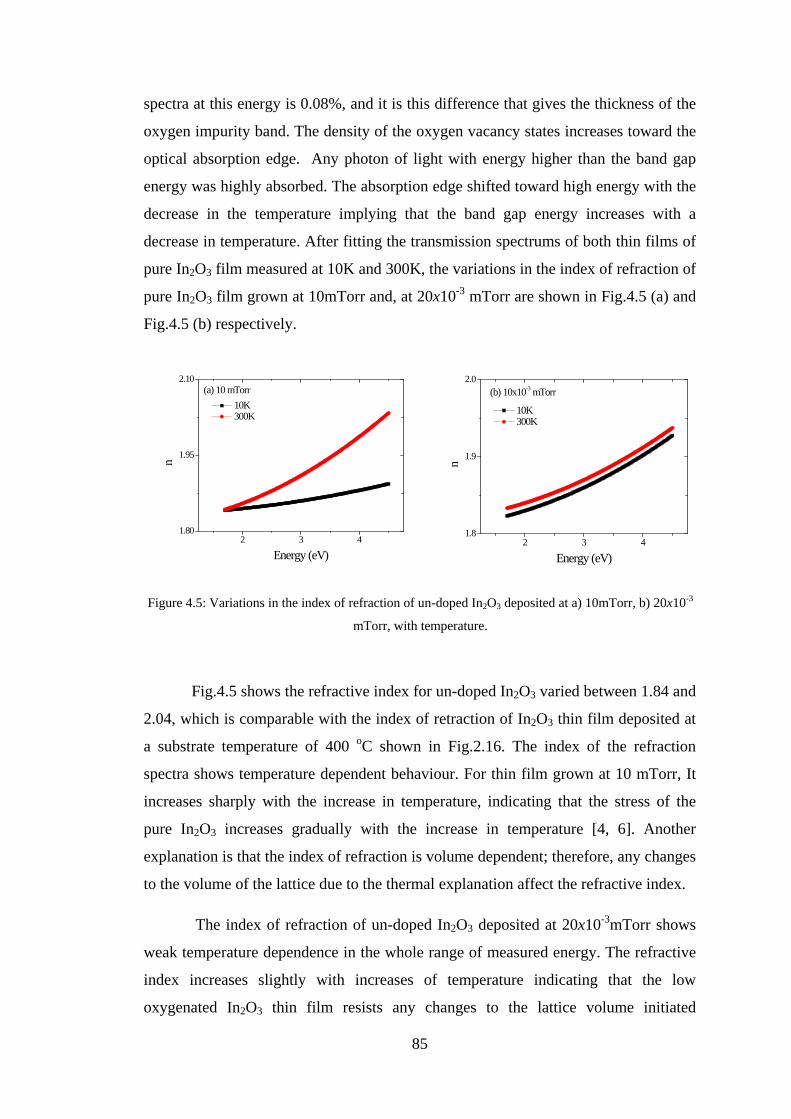
85
spectra at this energy is 0.08%, and it is this difference that gives the thickness of the
oxygen impurity band. The density of the oxygen vacancy states increases toward the
optical absorption edge. Any photon of light with energy higher than the band gap
energy was highly absorbed. The absorption edge shifted toward high energy with the
decrease in the temperature implying that the band gap energy increases with a
decrease in temperature. After fitting the transmission spectrums of both thin films of
pure In2O3 film measured at 10K and 300K, the variations in the index of refraction of
pure In2O3 film grown at 10mTorr and, at 20x10-3 mTorr are shown in Fig.4.5 (a) and
Fig.4.5 (b) respectively.
2 3 41.80
1.95
2.10
n
Energy (eV)
10K 300K
(a) 10 mTorr
2 3 41.8
1.9
2.0(b) 10x10-3 mTorr
n
Energy (eV)
10K 300K
Figure 4.5: Variations in the index of refraction of un-doped In2O3 deposited at a) 10mTorr, b) 20x10-3
mTorr, with temperature.
Fig.4.5 shows the refractive index for un-doped In2O3 varied between 1.84 and
2.04, which is comparable with the index of retraction of In2O3 thin film deposited at
a substrate temperature of 400 oC shown in Fig.2.16. The index of the refraction
spectra shows temperature dependent behaviour. For thin film grown at 10 mTorr, It
increases sharply with the increase in temperature, indicating that the stress of the
pure In2O3 increases gradually with the increase in temperature [4, 6]. Another
explanation is that the index of refraction is volume dependent; therefore, any changes
to the volume of the lattice due to the thermal explanation affect the refractive index.
The index of refraction of un-doped In2O3 deposited at 20x10-3mTorr shows
weak temperature dependence in the whole range of measured energy. The refractive
index increases slightly with increases of temperature indicating that the low
oxygenated In2O3 thin film resists any changes to the lattice volume initiated

86
thermally. The optical absorption coefficient spectrum as a function of temperature of
pure In2O3 film grown at 10mTorr and, at 20x10-3 mTorr are shown in Fig.4.6 (a) and
Fig.4.7 (b) respectively.
2 3 40
5
10
15
(a) 10 mTorr
0 100 200 3003.60
3.65
3.70
3.75
Ener
gy (e
V)
Temperature (K)
α (1
04 cm
-1)
Energy (eV)
10K 300K
2 3 40
5
10
15
(b) 20x10-3 mTorr
0 100 200 3003.7
3.8
3.9
Ener
gy (e
V)
Temperture (K)
α (1
04 cm
-1)
Energy (eV)
10K 300K
Figure 4.6: Variations in the optical absorption coefficient of un-doped In2O3 deposited at a) 10mTorr,
b) 20x10-3 mTorr, with temperature; the inset shows the optical band gap as a function of temperature.
Fig.4.6 illustrates the absorption coefficient spectra as a function of
temperature for un-doped In2O3 thin film deposited in (a) a high and (b) a low oxygen
environment. The spectra show no energy band below 3.0eV, which clarifies the
transparent region of In2O3. In the range between 3.0eV and the optical absorption
edge, a layer of NBE levels of oxygen vacancies was formed. The density of the
oxygen vacancy states increased toward the optical absorption edge of the In2O3 thin
film. The optical absorption edge shifted toward high energy as the temperature
decreased. The optical band gap energy as a function of temperature is shown in an
inset of Fig. 4.6. The optical band gap at room temperature is consistent with what is
expected of thin film deposited at a substrate temperature higher than 400 oC, as
shown in Fig.2.15. The optical band gap energy increases with decreases in
temperature, which is consistent with what is expected for variations in optical band
gap energy with the temperature of the semiconductor, following the Varshni formula
[7]. When the shift in energy between the optical absorption edges at 10K and RT is
eliminated, then the optical absorption coefficient spectra are shown to be temperature
independent. The scaled temperature dependence of the optical absorption coefficient
spectra of pure In2O3 film grown at 10mTorr and, at 20x10-3 mTorr are shown in
Fig.4.7 (a) and Fig.4.7 (b) respectively.
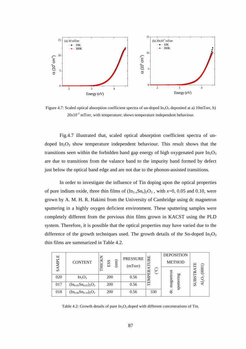
87
2 3 40
5
10
15 (a) 10 mTorr
α (1
04 cm
-1)
Energy (eV)
10K 300K
2 3 40
5
10
15(b) 20x10-3 mTorr
α (1
04 cm
-1)
Energy (eV)
10K 300K
Figure 4.7: Scaled optical absorption coefficient spectra of un-doped In2O3 deposited at a) 10mTorr, b)
20x10-3 mTorr, with temperature; shows temperature independent behaviour.
Fig.4.7 illustrated that, scaled optical absorption coefficient spectra of un-
doped In2O3 show temperature independent behaviour. This result shows that the
transitions seen within the forbidden band gap energy of high oxygenated pure In2O3
are due to transitions from the valance band to the impurity band formed by defect
just below the optical band edge and are not due to the phonon-assisted transitions.
In order to investigate the influence of Tin doping upon the optical properties
of pure indium oxide, three thin films of (In1-xSnx)2O3 , with x=0, 0.05 and 0.10, were
grown by A. M. H. R. Hakimi from the University of Cambridge using dc magnetron
sputtering in a highly oxygen deficient environment. These sputtering samples were
completely different from the previous thin films grown in KACST using the PLD
system. Therefore, it is possible that the optical properties may have varied due to the
difference of the growth techniques used. The growth details of the Sn-doped In2O3
thin films are summarized in Table 4.2.
SAM
PLE
CONTENT
THIC
KN
ESS
(nm
) PRESSURE
(mTorr)
TEM
PER
ATU
RE
(˚C)
DEPOSITION
METHOD
SUB
STR
ATE
Al 2O
3 (00
01)
dc. m
agne
tron
sput
terin
g
020 In2O3 200 0.56
017 (In0.95Sn0.05)2O3 200 0.56
018 (In0.90Sn0.10)2O3 200 0.56 330
Table 4.2: Growth details of pure In2O3 doped with different concentrations of Tin.
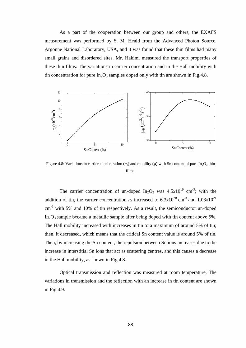
88
As a part of the cooperation between our group and others, the EXAFS
measurement was performed by S. M. Heald from the Advanced Photon Source,
Argonne National Laboratory, USA, and it was found that these thin films had many
small grains and disordered sites. Mr. Hakimi measured the transport properties of
these thin films. The variations in carrier concentration and in the Hall mobility with
tin concentration for pure In2O3 samples doped only with tin are shown in Fig.4.8.
0 5 10
2
4
6
8
10
12
n c (x1
020cm
-3)
Sn Content (%)
0 5 1030
35
40
µ H (c
m2 V-1
s-1)
Sn Content (%)
Figure 4.8: Variations in carrier concentration (nc) and mobility (μ) with Sn content of pure In2O3 thin
films.
The carrier concentration of un-doped In2O3 was 4.5x1019 cm-3; with the
addition of tin, the carrier concentration nc increased to 6.3x1020 cm-3 and 1.03x10²¹
cm-3 with 5% and 10% of tin respectively. As a result, the semiconductor un-doped
In2O3 sample became a metallic sample after being doped with tin content above 5%.
The Hall mobility increased with increases in tin to a maximum of around 5% of tin;
then, it decreased, which means that the critical Sn content value is around 5% of tin.
Then, by increasing the Sn content, the repulsion between Sn ions increases due to the
increase in interstitial Sn ions that act as scattering centres, and this causes a decrease
in the Hall mobility, as shown in Fig.4.8.
Optical transmission and reflection was measured at room temperature. The
variations in transmission and the reflection with an increase in tin content are shown
in Fig.4.9.
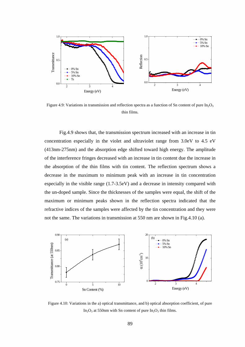
89
2 3 40.0
0.5
1.0
Tran
smitt
ance
Energy (eV)
0% Sn 5% Sn 10% Sn Ts
2 3 40.0
0.5
1.0
Refle
ction
Energy (eV)
0% Sn 5% Sn 10% Sn
Figure 4.9: Variations in transmission and reflection spectra as a function of Sn content of pure In2O3
thin films.
Fig.4.9 shows that, the transmission spectrum increased with an increase in tin
concentration especially in the violet and ultraviolet range from 3.0eV to 4.5 eV
(413nm-275nm) and the absorption edge shifted toward high energy. The amplitude
of the interference fringes decreased with an increase in tin content due the increase in
the absorption of the thin films with tin content. The reflection spectrum shows a
decrease in the maximum to minimum peak with an increase in tin concentration
especially in the visible range (1.7-3.5eV) and a decrease in intensity compared with
the un-doped sample. Since the thicknesses of the samples were equal, the shift of the
maximum or minimum peaks shown in the reflection spectra indicated that the
refractive indices of the samples were affected by the tin concentration and they were
not the same. The variations in transmission at 550 nm are shown in Fig.4.10 (a).
0 5 100.75
0.80
0.85
0.90
Tran
smitt
ance
(at 5
50nm
)
Sn Content (%)
(a)
2 3 40
10
20
α (1
04 cm-1)
Energy (eV)
0% Sn 5% Sn 10% Sn
(b)
Figure 4.10: Variations in the a) optical transmittance, and b) optical absorption coefficient, of pure
In2O3 at 550nm with Sn content of pure In2O3 thin films.
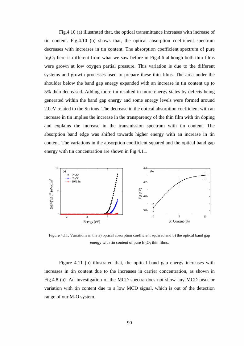
90
Fig.4.10 (a) illustrated that, the optical transmittance increases with increase of
tin content. Fig.4.10 (b) shows that, the optical absorption coefficient spectrum
decreases with increases in tin content. The absorption coefficient spectrum of pure
In2O3 here is different from what we saw before in Fig.4.6 although both thin films
were grown at low oxygen partial pressure. This variation is due to the different
systems and growth processes used to prepare these thin films. The area under the
shoulder below the band gap energy expanded with an increase in tin content up to
5% then decreased. Adding more tin resulted in more energy states by defects being
generated within the band gap energy and some energy levels were formed around
2.0eV related to the Sn ions. The decrease in the optical absorption coefficient with an
increase in tin implies the increase in the transparency of the thin film with tin doping
and explains the increase in the transmission spectrum with tin content. The
absorption band edge was shifted towards higher energy with an increase in tin
content. The variations in the absorption coefficient squared and the optical band gap
energy with tin concentration are shown in Fig.4.11.
2 3 40
50
100
(αhν
)2 x10¹⁰
(eV/
cm)2
Energy (eV)
0% Sn 5% Sn 10% Sn
(a)
0 5 10
3.8
4.0
4.2
4.4
Eg (e
V)
Sn Content (%)
(b)
Figure 4.11: Variations in the a) optical absorption coefficient squared and b) the optical band gap
energy with tin content of pure In2O3 thin films.
Figure 4.11 (b) illustrated that, the optical band gap energy increases with
increases in tin content due to the increases in carrier concentration, as shown in
Fig.4.8 (a). An investigation of the MCD spectra does not show any MCD peak or
variation with tin content due to a low MCD signal, which is out of the detection
range of our M-O system.
91
4.3 Conclusion This chapter investigated the influence the oxygen partial pressure and tin
doping on the optical properties of pure In2O3 thin films. Variations in oxygen partial
pressure during the growth process lead to the formation or disappearance of oxygen
impurity bands located below the optical absorption edge. Decreasing the oxygen
partial pressure leads to the development of oxygen impurity bands, an increase in the
carrier density, and the shifting of the optical band gap towards higher energy. The
transmission drops in the range of energy located below the optical band gap energy,
which is supported by the increases in the absorption coefficient in the same range of
energy, indicating that the transitions between the valance band and some bands
within the optical band gap are established. The origin of these transitions was
explored through the measurements of the optical properties as a function of
temperature. The few optical studies of In2O3 thin films reported to date have been at
room temperate and this is the first optical study has considered the temperature
dependence for doped or un-doped In2O3. These investigations included thin films
prepared in high and low oxygen partial pressure atmospheres. Both showed and
confirmed that the transitions seen within the forbidden band gap energy are
temperature independent and due to the transitions from the valance band to the donor
levels by defects (oxygen impurity bands) and not due to the thermal activation of
phonons. Therefore, the oxygen impurity bands are an active partner in any MCD
signal that may exist between 3.0eV and the optical band gap energy of In2O3.
The influence of tin doping on the optical properties of pure In2O3 was also
discussed. We found that doping with tin leads to an increase in the carrier density
and the density of the donor bands. Therefore, the carrier density and the density of
the oxygen impurity bands can be increased by growing thin films at low oxygen
pressure, through the vacuum annealing process, or by doping with tin; the low
oxygen pressure method is more effective than the annealing process method. In the
case of TM-doped In2O3, this situation may change as some of these methods may
lead to the formation of TM nanoparticles, as we are going to find out in the next
chapters.

92
4.4 References 1. R. Swanepoel, J. Phys. E: Scientific Instruments 16, 1214 (1983).
2. B. P. Chandra, and S. C. Bhaiya, American J. Phys. 51, 160-161 (1983).
3. S. A. Khodier, Optics & Laser Technology 34, 125-128 (2002).
4. P. Prathap, Y. P. V. Subbaiah, M. Devika and K. T. R. Reddy, Mater. Chem.
Phys. 100, 375-379 (2006).
5. J. Tauc, Amorphous and liquid semiconductors 1974, London, New York,:
Plenum. ix, 441 p.
6. H. Poelman, D. Poelman, D. Depla, H. Tomaszewski, L. Fiermans and R. De
Gryse, Surface Science 482-485, 940-945 (2001).
7. S. Adachi, Physical properties of III-V semiconductor compounds : InP, InAs,
GaAs, GaP, InGaAs, and InGaAsP 1992, New York: Wiley. xviii, 318 p.
93
Chapter 5 – Maxwell-Garnett Theory
5.1 Introduction
The ferromagnetism in oxide magnetic semiconductors usually induced by
clustered magnetic impurities [1] or attributed to the oxygen vacancy defects [2, 3] or
attributed to the formation of TM nanoparticles. The presence of metallic or
nanoparticles TM is always expected, especially for Co-, and Fe-doped In2O3. This
chapter develop a lab-based alternative to EXAFS and represent and use the Maxwell-
Garnett (M-G) theory to determine the fraction and the contribution of TM
nanoparticles to the total magnetic and magneto-optical properties of TM-doped In2O3
thin films where the existence of TM nanoparticles is confirmed.
5.2 Co Nanoparticles
C. Clavero et al. investigated the optical and magneto-optical properties of Co
nanoparticles embedded in ZrO2 in the spectral range from 1.4 to 4.3 eV[4]. They
used the effective medium approximation [5], which takes into account the Co
concentration dependence for the Co nanoparticles with a size much smaller than the
wavelength of the incident light, and they used the Maxwell-Garnett approximation,
which was originally an effective-medium theory but was developed by Maxwell-
Garnett for a composite composed of particles embedded in a host on the assumption
that the total polarization would be the same as the sum of the polarization
contributions from the embedded particles. Therefore, the Maxwell-Garnett
approximation calculates the effective dielectric tensor . The effective dielectric
tensor represents a composite material consisting of particles randomly distributed in
a matrix depending on the dielectric tensors of the particles and matrix, and the
concentration and shape of the particles[6].
The expression for the elements of the dielectric tensor for cobalt metal is in
the form
200
0
0
ˆ1
1
i
i
Equation(5.1)
94
where all the elements are complex. The theoretical expressions for these
elements are given using a Drude theory [7] as follows:
[ ]
Equation(5.2)
[ ]
Equation(5.3)
where
is the cyclotron frequency,
is the plasma
frequency, being the conduction band electron density and the electron effective
mass. is the relaxation time of the electrons, which depends on the electron-electron,
electron-phonon, and electron-defect scattering contributions [8].
Since the in the range of spectrum that we are
interested in, therefore, the expressions of the elements of the dielectric tensor of
cobalt become:
Equation(5.4)
[ ]
[ ] Equation(5.5)
by putting the elements of the dielectric tensor of cobalt in their real and
imaginary parts, as follows:
Equation(5.6)
Equation(5.7)
where the parameters have the following expressions:
Equation(5.8)
[ ] Equation(5.9)
Equation(5.10)

95
Equation(5.11)
These equations were derived by my supervisor Gillian Gehring for metallic
Co. The parameters and were obtained by Krinchik for Co [9-11]. The
values of these parameters for Co were
. These values were used to plot the expressions of Equ.5.10 and Equ.5.11
in the energy range of (1.5eV to 4.2eV). The real and imaginary parts of the off
diagonal elements of the dielectric tensor of cobalt are shown in Fig.5.1.
2 3 4-0.2
-0.1
0.0
0.1
Re
(C
o)
Energy (eV)
2 3 4
0.0
0.5
1.0
Im (C
o)
Energy (eV)
Figure 5.1: The real and imaginary parts of the Off diagonal elements of the dielectric tensor of cobalt.
These data are in agreement with those calculated for cobalt by Krinchik [9]
and Clavero [11]. However, the real and imaginary parts of off diagonal elements
calculated for bulk cobalt by Clavero were switched; he used a different definition for
the off diagonal elements with and rather than and , as follows:
zz
xxxy
xyxx
00
0
0~
Equation(5.12)
The Maxwell-Garnett theory was used to calculate the expected response of
cobalt nanoparticles in a non-magnetic In2O3 medium. The effective dielectric tensor
in terms of the parameters is:

96
[ (
)]
[ (
)]
Equation(5.13)
where represents the volume fraction of metallic Co embedded in the host
material. represents the shape factors, which have been reported for Co
nanoparticles in the MgO host as and [11].
(
)
Equation(5.14)
(
(
) )
Equation(5.15)
By considering new parameters and , where
(
)
(
)
Equation(5.16)
(
( )
)
Equation(5.17)
then, the effective dielectric tensor becomes
Equation(5.18)
where the real and imaginary parts of the effective dielectric tensor of Co in
In2O3 host matrix are
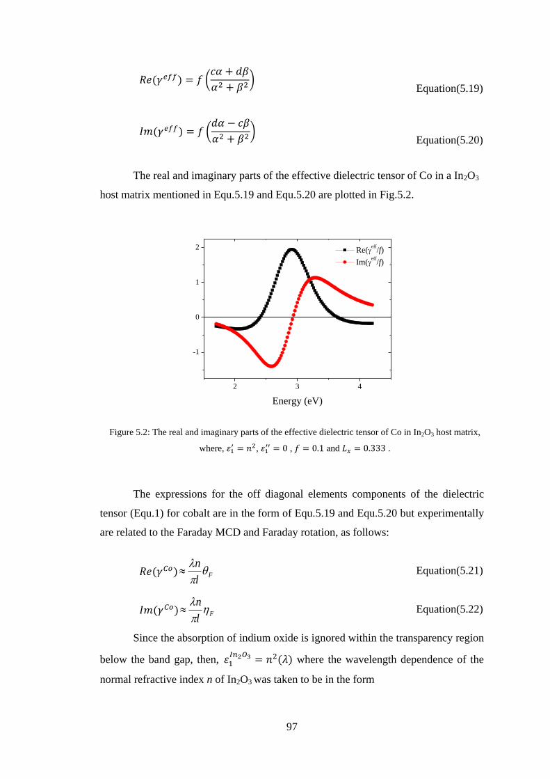
97
(
)
Equation(5.19)
(
)
Equation(5.20)
The real and imaginary parts of the effective dielectric tensor of Co in a In2O3
host matrix mentioned in Equ.5.19 and Equ.5.20 are plotted in Fig.5.2.
2 3 4
-1
0
1
2
Energy (eV)
Re(eff
/f)
Im(eff
/f)
Figure 5.2: The real and imaginary parts of the effective dielectric tensor of Co in In2O3 host matrix,
where, ,
, and .
The expressions for the off diagonal elements components of the dielectric
tensor (Equ.1) for cobalt are in the form of Equ.5.19 and Equ.5.20 but experimentally
are related to the Faraday MCD and Faraday rotation, as follows:
Fl
n
Equation(5.21)
Fl
n
Equation(5.22)
Since the absorption of indium oxide is ignored within the transparency region
below the band gap, then, where the wavelength dependence of the
normal refractive index n of In2O3 was taken to be in the form
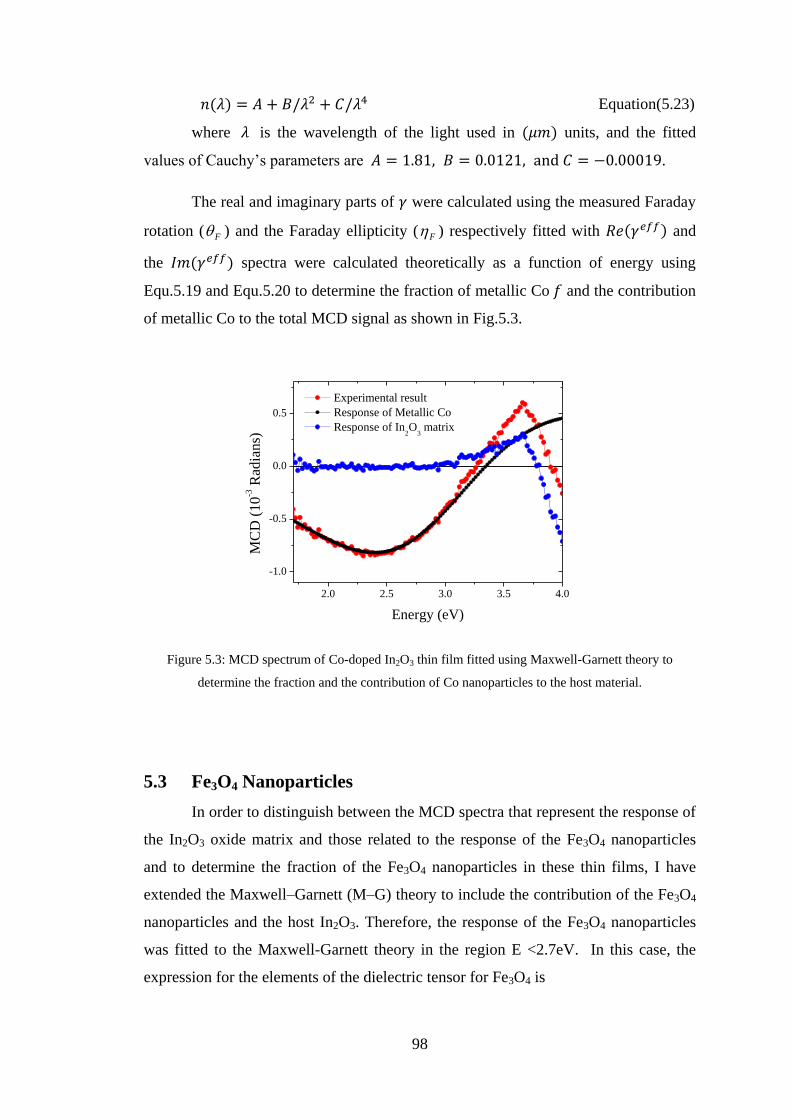
98
Equation(5.23)
where is the wavelength of the light used in units, and the fitted
values of Cauchy’s parameters are .
The real and imaginary parts of were calculated using the measured Faraday
rotation ( F ) and the Faraday ellipticity ( F ) respectively fitted with and
the spectra were calculated theoretically as a function of energy using
Equ.5.19 and Equ.5.20 to determine the fraction of metallic Co and the contribution
of metallic Co to the total MCD signal as shown in Fig.5.3.
2.0 2.5 3.0 3.5 4.0
-1.0
-0.5
0.0
0.5
Experimental result
Response of Metallic Co
Response of In2O
3 matrix
MC
D (
10
-3 R
adia
ns)
Energy (eV)
Figure 5.3: MCD spectrum of Co-doped In2O3 thin film fitted using Maxwell-Garnett theory to
determine the fraction and the contribution of Co nanoparticles to the host material.
5.3 Fe3O4 Nanoparticles
In order to distinguish between the MCD spectra that represent the response of
the In2O3 oxide matrix and those related to the response of the Fe3O4 nanoparticles
and to determine the fraction of the Fe3O4 nanoparticles in these thin films, I have
extended the Maxwell–Garnett (M–G) theory to include the contribution of the Fe3O4
nanoparticles and the host In2O3. Therefore, the response of the Fe3O4 nanoparticles
was fitted to the Maxwell-Garnett theory in the region E <2.7eV. In this case, the
expression for the elements of the dielectric tensor for Fe3O4 is

99
zz
xxxy
xyxx i
~00
0~~0~~
~ Equation(5.24)
and the effective dielectric function for light propagation along the direction of
magnetization, z, is given by
[
]
Equation(5.25)
where
Equation(5.26)
Equation(5.27)
Since below the optical band gap, therefore, Equ.5.27 becomes
Equation(5.28)
Substituting Equ.5.28 in Equ.5.26 leads to
Equation(5.29)
is the fraction of Fe3O4 nanoparticles in the sample and usually is very small
; therefore, . is the demagnetising factor. Both and are
treated as fitting parameters. The fitted value of is then compared with the value
obtained from EXAFS. Equ.5.25 becomes
[
]
Equation(5.30)
If we assume is very small, then,
; therefore,
Equ.5.30 becomes
[
]
Equation(5.31)
Since we are interested in the imaginary part of the dielectric tensor,
Equ.5.31becomes
100
[
]
Equation(5.32)
For Fe ions
Equation(5.33)
Equation(5.34)
By rewriting Equ.5.32 taking into consideration Equ.9:
[
]
Equation(5.35)
By letting
Equation(5.36)
Equ.5.35 becomes
[
] Equation(5.37)
By considering new variables where
Equation(5.38)
Equation(5.39)
Equation(5.40)
Equation(5.41)
By substituting Equ.5.38, 5.39, 5.40, and 5.41 in Equ.5.37
[ ] Equation(5.42)
Solving Equ.5.42 for the imaginary part of
leads to
[ ]
Equation(5.43)
101
By putting
, the part
in Equ.5.43 becomes
Equation(5.44)
By putting Equ.5.44 in Equ.5.43, then
Equation(5.45)
Equation(5.46)
Since we assumed that is very small, the part
can be
ignored. As a result, Equ.5.46 becomes
Equation(5.47)
The values of and are calculated from Equ.13, where, is a fitting
parameter and the index of refraction as a function of energy is obtained from the
Swanepoel method, explained in section 3.9, for pure In2O3 thin film grown under the
same growth conditions, which in this case was at low oxygen pressure, as given in
chapter 4. The values of and are calculated from the real ( ) and imaginary
( ) part of the diagonal element of the dielectric tensor of Fe3O4 as mentioned in
Equ.5.33, Equ.5.38 and Equ.5.39, where the real ( ) and imaginary (
) parts of
the diagonal element of the dielectric tensor of Fe3O4 are a function of energy, as
shown in Fig.5.4.
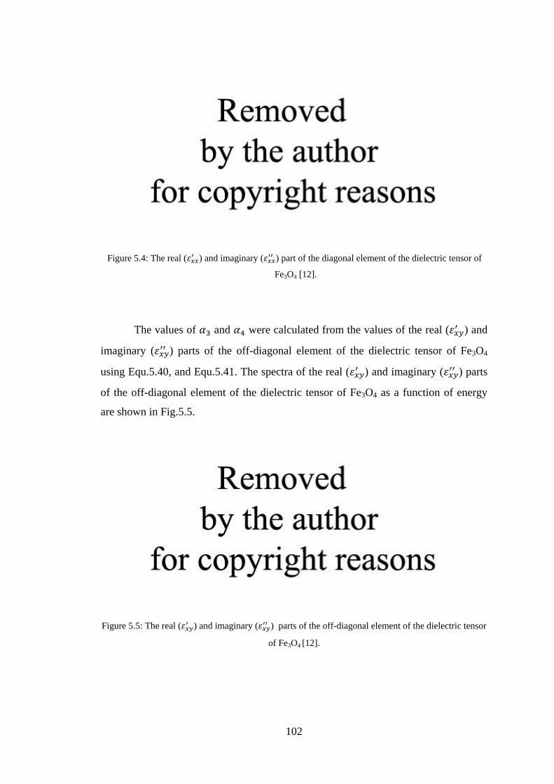
102
Figure 5.4: The real ( ) and imaginary (
) part of the diagonal element of the dielectric tensor of
Fe3O4 [12].
The values of and were calculated from the values of the real ( ) and
imaginary ( ) parts of the off-diagonal element of the dielectric tensor of Fe3O4
using Equ.5.40, and Equ.5.41. The spectra of the real ( ) and imaginary (
) parts
of the off-diagonal element of the dielectric tensor of Fe3O4 as a function of energy
are shown in Fig.5.5.
Figure 5.5: The real ( ) and imaginary (
) parts of the off-diagonal element of the dielectric tensor
of Fe3O4 [12].
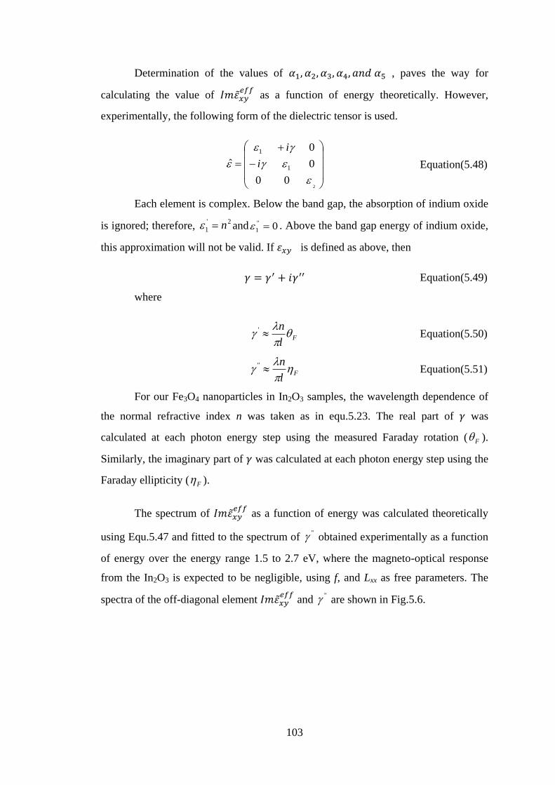
103
Determination of the values of , paves the way for
calculating the value of
as a function of energy theoretically. However,
experimentally, the following form of the dielectric tensor is used.
200
0
0
ˆ1
1
i
i
Equation(5.48)
Each element is complex. Below the band gap, the absorption of indium oxide
is ignored; therefore, 2'
1 n and 0''
1 . Above the band gap energy of indium oxide,
this approximation will not be valid. If is defined as above, then
Equation(5.49)
where
Fl
n
'
Equation(5.50)
Fl
n
''
Equation(5.51)
For our Fe3O4 nanoparticles in In2O3 samples, the wavelength dependence of
the normal refractive index n was taken as in equ.5.23. The real part of was
calculated at each photon energy step using the measured Faraday rotation ( F ).
Similarly, the imaginary part of was calculated at each photon energy step using the
Faraday ellipticity ( F ).
The spectrum of
as a function of energy was calculated theoretically
using Equ.5.47 and fitted to the spectrum of '' obtained experimentally as a function
of energy over the energy range 1.5 to 2.7 eV, where the magneto-optical response
from the In2O3 is expected to be negligible, using f, and Lxx as free parameters. The
spectra of the off-diagonal element
and '' are shown in Fig.5.6.
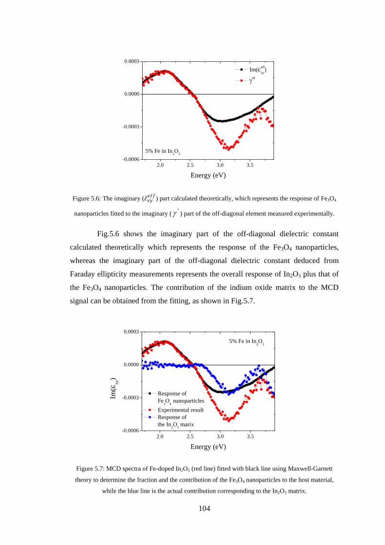
104
2.0 2.5 3.0 3.5-0.0006
-0.0003
0.0000
0.0003
Energy (eV)
Im(eff
xy)
''
5% Fe in In2O
3
Figure 5.6: The imaginary (
) part calculated theoretically, which represents the response of Fe3O4
nanoparticles fitted to the imaginary ('' ) part of the off-diagonal element measured experimentally.
Fig.5.6 shows the imaginary part of the off-diagonal dielectric constant
calculated theoretically which represents the response of the Fe3O4 nanoparticles,
whereas the imaginary part of the off-diagonal dielectric constant deduced from
Faraday ellipticity measurements represents the overall response of In2O3 plus that of
the Fe3O4 nanoparticles. The contribution of the indium oxide matrix to the MCD
signal can be obtained from the fitting, as shown in Fig.5.7.
2.0 2.5 3.0 3.5-0.0006
-0.0003
0.0000
0.0003
5% Fe in In2O
3
Im(
xy)
Energy (eV)
Response of
Fe3O
4 nanoparticles
Experimental result
Response of
the In2O
3 marix
Figure 5.7: MCD spectra of Fe-doped In2O3 (red line) fitted with black line using Maxwell-Garnett
theory to determine the fraction and the contribution of the Fe3O4 nanoparticles to the host material,
while the blue line is the actual contribution corresponding to the In2O3 matrix.
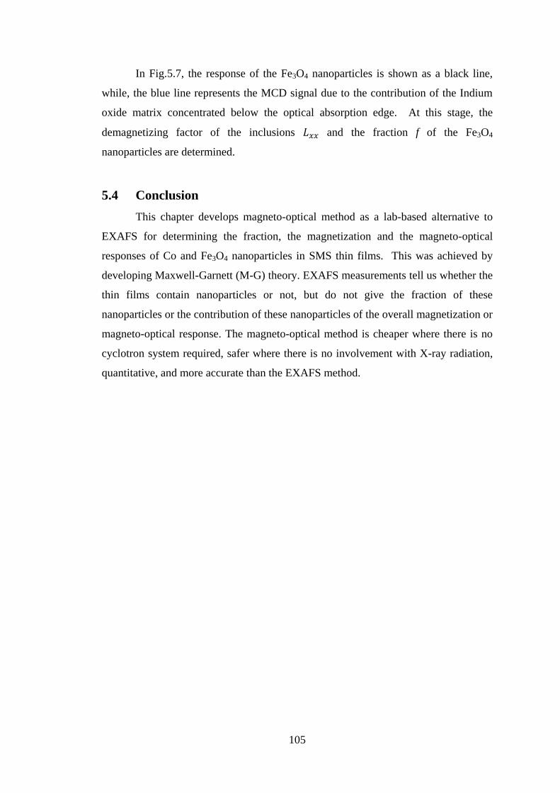
105
In Fig.5.7, the response of the Fe3O4 nanoparticles is shown as a black line,
while, the blue line represents the MCD signal due to the contribution of the Indium
oxide matrix concentrated below the optical absorption edge. At this stage, the
demagnetizing factor of the inclusions and the fraction f of the Fe3O4
nanoparticles are determined.
5.4 Conclusion
This chapter develops magneto-optical method as a lab-based alternative to
EXAFS for determining the fraction, the magnetization and the magneto-optical
responses of Co and Fe3O4 nanoparticles in SMS thin films. This was achieved by
developing Maxwell-Garnett (M-G) theory. EXAFS measurements tell us whether the
thin films contain nanoparticles or not, but do not give the fraction of these
nanoparticles or the contribution of these nanoparticles of the overall magnetization or
magneto-optical response. The magneto-optical method is cheaper where there is no
cyclotron system required, safer where there is no involvement with X-ray radiation,
quantitative, and more accurate than the EXAFS method.
106
5.5 References
1. J. Y. Kim, J. H. Park, B. G. Park, H. J. Noh, S. J. Oh, J. S. Yang, D. H. Kim,
S. D. Bu, T. W. Noh, H. J. Lin, H. H. Hsieh and C. T. Chen, Physical Review
Letters 90, 017401 (2003).
2. J. M. D. Coey, A. P. Douvalis, C. B. Fitzgerald and M. Venkatesan, Applied
Physics Letters 84, 1332-1334 (2004).
3. J. M. D. Coey, M. Venkatesan and C. B. Fitzgerald, Nat Mater 4, 173-179
(2005).
4. C. Clavero, B. Sepúlveda, G. Armelles, Z. Konstantinovi, M. G. d. Muro, A.
Labarta and X. Batlle, Vol. 100. 2006: AIP. 074320.
5. D. Stroud, Physical Review B 12, 3368 (1975).
6. J. S. Ahn, K. H. Kim, T. W. Noh, D. H. Riu, K. H. Boo and H. E. Kim,
Physical Review B 52, 15244 (1995).
7. P. B. Johnson and R.W. Christy, Physical Review B 6, 4370 (1972).
8. N. D. Fatti, F. Vallée, C. Flytzanis, Y. Hamanaka and A. Nakamura, Chemical
Physics 251, 215-226 (2000).
9. G.S. Krinchik, Vol. 35. 1964: AIP. 1089-1092.
10. R. Carey and B. W. J. Thomas, Journal of Physics D: Applied Physics 7, 2362
(1974).
11. C. Clavero, A. Cebollada, G. Armelles, Y. Huttel, J. Arbiol, F. Peiró and A.
Cornet, Phys Rev 72, 02441 (2005).
12. W. F. J. Fontijn, P. J. V. D. Zaag, M. A. C. Devillers, V. A. M. Brabers and
R. Metselaar, Physical Review B 56, 5432 (1997).
107
Chapter 6 – Co Doped In2O3
6.1 Introduction The transition metal (TM) doped semiconductor oxide was found to show
ferromagnetism at room temperature [1-10]. The ferromagnetism in semi magnetic
semiconductors (SMS) is usually attributed to the interaction between the host s, p
bands carriers and the localized 3d electrons in doped transition metal elements.
Several theoretical models have been suggested based on the s(p)-d interactions
feature, and these fall into two categories: the first category is the carrier-mediated
models like the Zener model and the Ruderman-Kittel-Kasuya-Yosida (RKKY)
model [11, 12]. In the carrier-mediated models, the coupling between magnetic ions is
achieved through the mobile carriers, i.e., holes in the valence band or electrons in the
conduction band. The second category is the super exchange models like the double-
exchange model [13-16]. In super exchange models, the coupling is achieved
between magnetic ions through the localized carriers.
This chapter investigates the optical and magneto optical response of the Co-
doped In2O3 thin films deposited in different growth conditions, and compares the
result with that obtained previously for a pure In2O3 thin film in order to assess the
effect of the Co doping. The Maxwell-Garnett (M-G) theory discussed in last chapter
is used to determine the fraction and the magneto-optical response of metallic Co in
some thin films where the existence of metallic Co is confirmed. The influence of co-
doping In2O3 with Co plus Sn simultaneously is also covered.
6.2 Experiment Details, Results, and Discussion In order to investigate the influence of Co doping content on the optical and
magneto-optical properties of In2O3, Five thin films of (In1-xCox)2O3 with 𝑥 = 0.01,
0.02, 0.03, 0.04, 0.05 were deposited by A. Hakimi in the University of Cambridge.
The thin films were grown in a highly oxygen deficient environment using dc
magnetron sputtering on sapphire substrate at 300 oC. Pure In2O3 thin films were also
grown at the same time under the same conditions as the Co-doped samples and
served as a set of control samples. The data described in this section have been
published [17]. The deposition details are shown in Table.6.1.
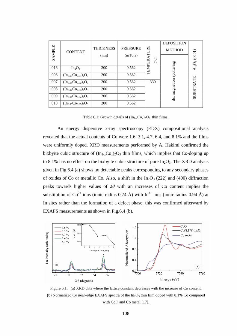
108
SAM
PLE
CONTENT THICKNESS
(nm)
PRESSURE
(mTorr)
TEM
PER
ATU
RE
(˚C
)
DEPOSITION
METHOD
SUB
STR
ATE
Al 2O
3 (00
01)
dc. m
agne
tron
sput
terin
g
016 In2O3 200 0.562
006 (In0.99Co0.01)2O3 200 0.562
007 (In0.98Co0.02)2O3 200 0.562 330
008 (In0.97Co0.03)2O3 200 0.562
009 (In0.96Co0.04)2O3 200 0.562
010 (In0.95Co0.05)2O3 200 0.562
Table 6.1: Growth details of (In1-xCox)2O3 thin films.
An energy dispersive x-ray spectroscopy (EDX) compositional analysis
revealed that the actual contents of Co were 1.6, 3.1, 4.7, 6.4, and 8.1% and the films
were uniformly doped. XRD measurements performed by A. Hakimi confirmed the
bixbyite cubic structure of (In1-xCox)2O3 thin films, which implies that Co-doping up
to 8.1% has no effect on the bixbyite cubic structure of pure In2O3. The XRD analysis
given in Fig.6.4 (a) shows no detectable peaks corresponding to any secondary phases
of oxides of Co or metallic Co. Also, a shift in the In2O3 (222) and (400) diffraction
peaks towards higher values of 2θ with an increases of Co content implies the
substitution of Co2+ ions (ionic radius 0.74 Å) with In3+ ions (ionic radius 0.94 Å) at
In sites rather than the formation of a defect phase; this was confirmed afterward by
EXAFS measurements as shown in Fig.6.4 (b).
Figure 6.1: (a) XRD data where the lattice constant decreases with the increase of Co content.
(b) Normalized Co near-edge EXAFS spectra of the In2O3 thin film doped with 8.1% Co compared
with CoO and Co metal [17].
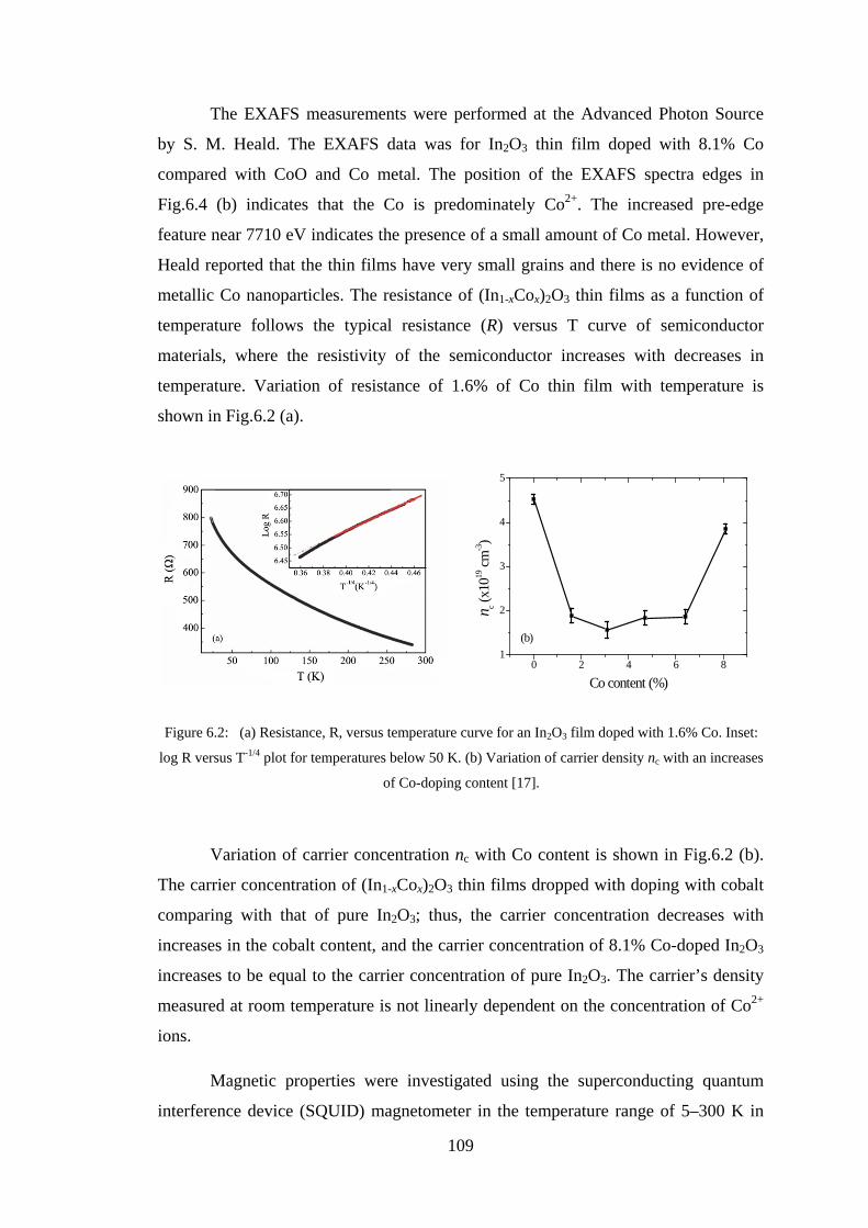
109
The EXAFS measurements were performed at the Advanced Photon Source
by S. M. Heald. The EXAFS data was for In2O3 thin film doped with 8.1% Co
compared with CoO and Co metal. The position of the EXAFS spectra edges in
Fig.6.4 (b) indicates that the Co is predominately Co2+. The increased pre-edge
feature near 7710 eV indicates the presence of a small amount of Co metal. However,
Heald reported that the thin films have very small grains and there is no evidence of
metallic Co nanoparticles. The resistance of (In1-xCox)2O3 thin films as a function of
temperature follows the typical resistance (R) versus T curve of semiconductor
materials, where the resistivity of the semiconductor increases with decreases in
temperature. Variation of resistance of 1.6% of Co thin film with temperature is
shown in Fig.6.2 (a).
0 2 4 6 8
1
2
3
4
5
(b)
n c (x1
019 cm
-3)
Co content (%)
Figure 6.2: (a) Resistance, R, versus temperature curve for an In2O3 film doped with 1.6% Co. Inset:
log R versus T-1/4 plot for temperatures below 50 K. (b) Variation of carrier density nc with an increases
of Co-doping content [17].
Variation of carrier concentration nc with Co content is shown in Fig.6.2 (b).
The carrier concentration of (In1-xCox)2O3 thin films dropped with doping with cobalt
comparing with that of pure In2O3; thus, the carrier concentration decreases with
increases in the cobalt content, and the carrier concentration of 8.1% Co-doped In2O3
increases to be equal to the carrier concentration of pure In2O3. The carrier’s density
measured at room temperature is not linearly dependent on the concentration of Co2+
ions.
Magnetic properties were investigated using the superconducting quantum
interference device (SQUID) magnetometer in the temperature range of 5–300 K in
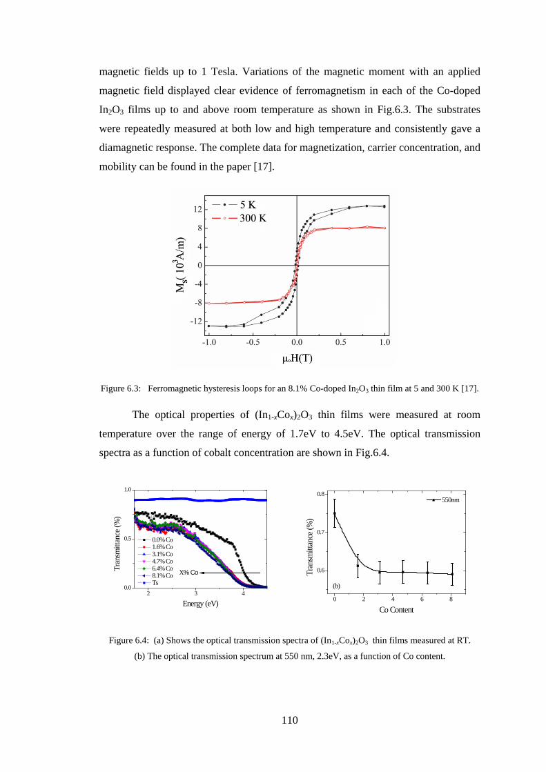
110
magnetic fields up to 1 Tesla. Variations of the magnetic moment with an applied
magnetic field displayed clear evidence of ferromagnetism in each of the Co-doped
In2O3 films up to and above room temperature as shown in Fig.6.3. The substrates
were repeatedly measured at both low and high temperature and consistently gave a
diamagnetic response. The complete data for magnetization, carrier concentration, and
mobility can be found in the paper [17].
Figure 6.3: Ferromagnetic hysteresis loops for an 8.1% Co-doped In2O3 thin film at 5 and 300 K [17].
The optical properties of (In1-xCox)2O3 thin films were measured at room
temperature over the range of energy of 1.7eV to 4.5eV. The optical transmission
spectra as a function of cobalt concentration are shown in Fig.6.4.
2 3 40.0
0.5
1.0
Tran
smitt
ance
(%)
Energy (eV)
0.0% Co 1.6% Co 3.1% Co 4.7% Co 6.4% Co 8.1% Co Ts
X% Co
0 2 4 6 8
0.6
0.7
0.8
Tran
smitt
ance
(%)
Co Content
550nm
(b)
Figure 6.4: (a) Shows the optical transmission spectra of (In1-xCox)2O3 thin films measured at RT.
(b) The optical transmission spectrum at 550 nm, 2.3eV, as a function of Co content.
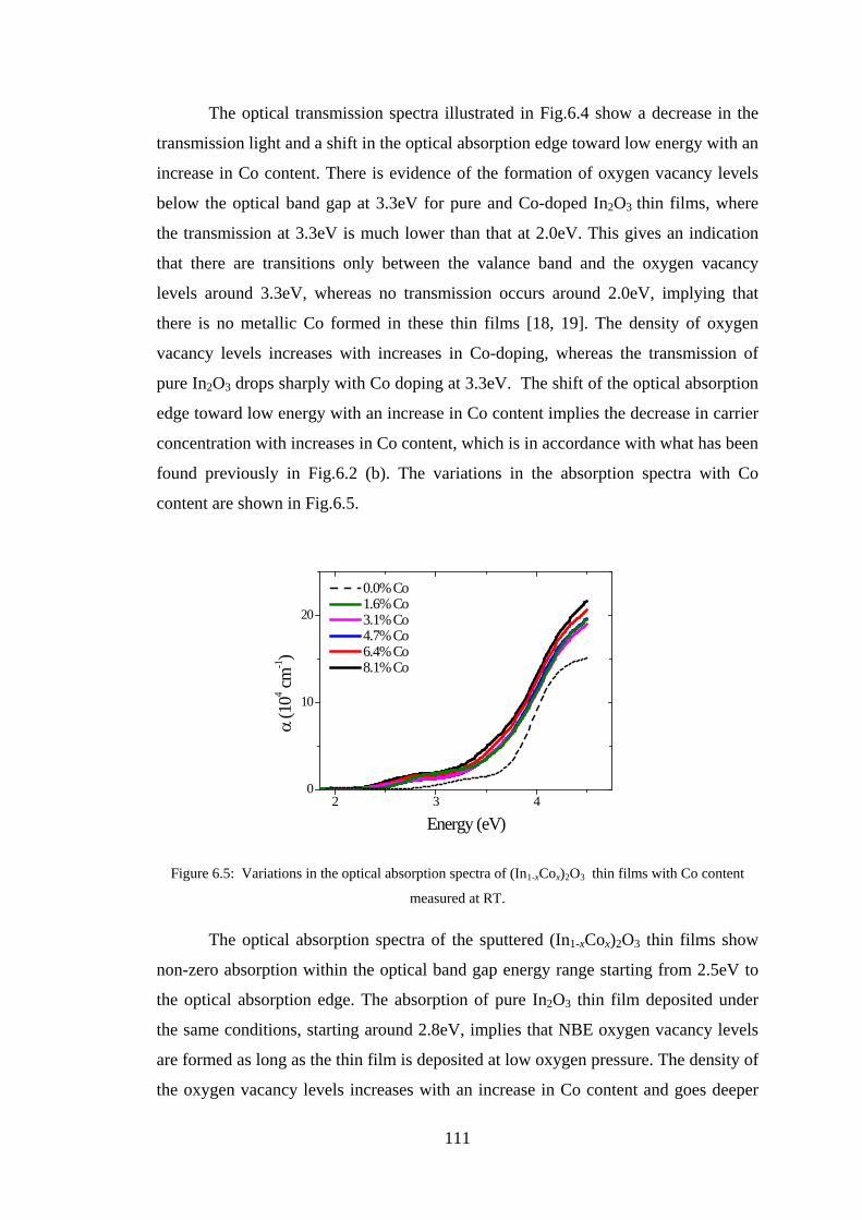
111
The optical transmission spectra illustrated in Fig.6.4 show a decrease in the
transmission light and a shift in the optical absorption edge toward low energy with an
increase in Co content. There is evidence of the formation of oxygen vacancy levels
below the optical band gap at 3.3eV for pure and Co-doped In2O3 thin films, where
the transmission at 3.3eV is much lower than that at 2.0eV. This gives an indication
that there are transitions only between the valance band and the oxygen vacancy
levels around 3.3eV, whereas no transmission occurs around 2.0eV, implying that
there is no metallic Co formed in these thin films [18, 19]. The density of oxygen
vacancy levels increases with increases in Co-doping, whereas the transmission of
pure In2O3 drops sharply with Co doping at 3.3eV. The shift of the optical absorption
edge toward low energy with an increase in Co content implies the decrease in carrier
concentration with increases in Co content, which is in accordance with what has been
found previously in Fig.6.2 (b). The variations in the absorption spectra with Co
content are shown in Fig.6.5.
0.0% Co 1.6% Co 3.1% Co 4.7% Co 6.4% Co 8.1% Co
2 3 40
10
20
α (1
04 cm-1)
Energy (eV)
Figure 6.5: Variations in the optical absorption spectra of (In1-xCox)2O3 thin films with Co content
measured at RT.
The optical absorption spectra of the sputtered (In1-xCox)2O3 thin films show
non-zero absorption within the optical band gap energy range starting from 2.5eV to
the optical absorption edge. The absorption of pure In2O3 thin film deposited under
the same conditions, starting around 2.8eV, implies that NBE oxygen vacancy levels
are formed as long as the thin film is deposited at low oxygen pressure. The density of
the oxygen vacancy levels increases with an increase in Co content and goes deeper
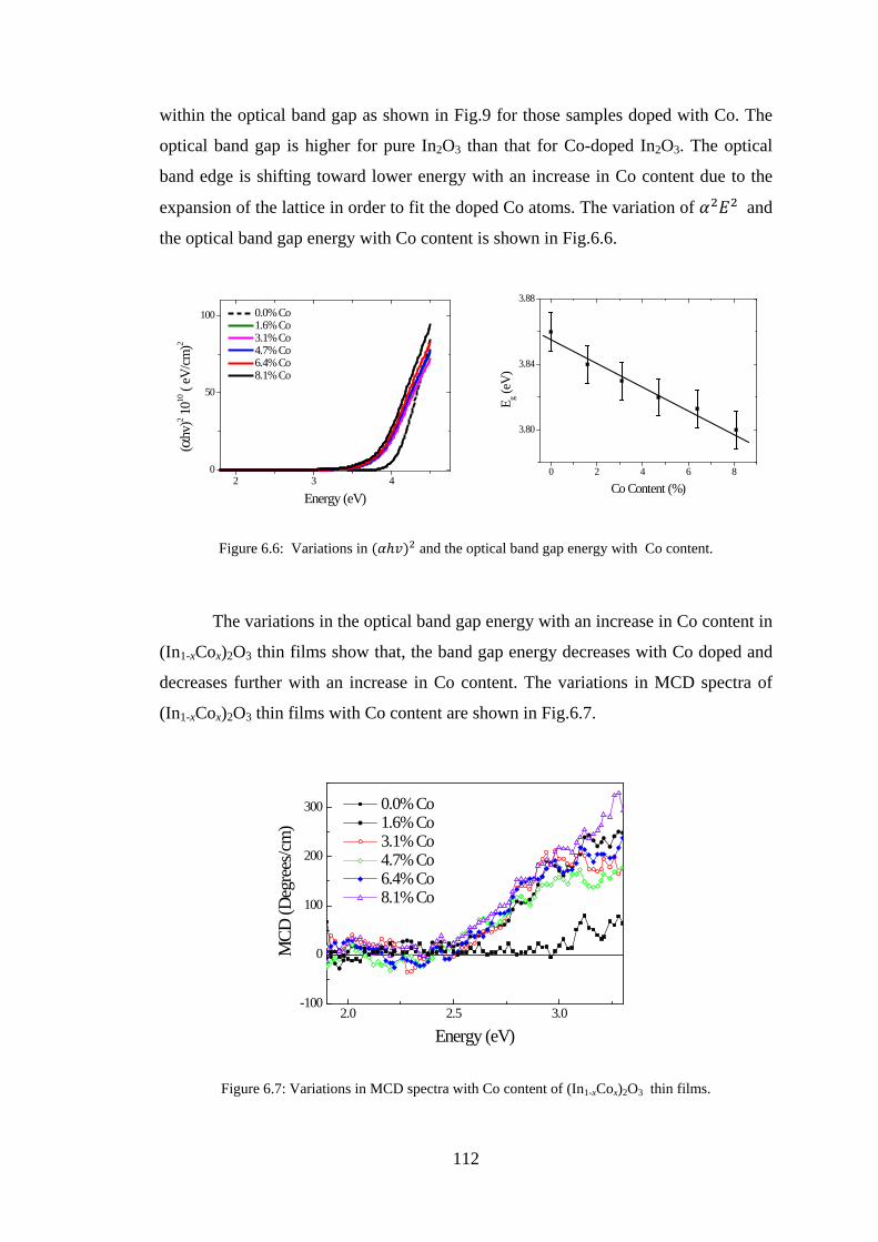
112
within the optical band gap as shown in Fig.9 for those samples doped with Co. The
optical band gap is higher for pure In2O3 than that for Co-doped In2O3. The optical
band edge is shifting toward lower energy with an increase in Co content due to the
expansion of the lattice in order to fit the doped Co atoms. The variation of 𝛼2𝐸2 and
the optical band gap energy with Co content is shown in Fig.6.6.
2 3 40
50
100
(αhv
)2 1010
( eV
/cm
)2
Energy (eV)
0.0% Co 1.6% Co 3.1% Co 4.7% Co 6.4% Co 8.1% Co
0 2 4 6 8
3.80
3.84
3.88
E g (eV
)Co Content (%)
Figure 6.6: Variations in (𝛼ℎ𝑣)2 and the optical band gap energy with Co content.
The variations in the optical band gap energy with an increase in Co content in
(In1-xCox)2O3 thin films show that, the band gap energy decreases with Co doped and
decreases further with an increase in Co content. The variations in MCD spectra of
(In1-xCox)2O3 thin films with Co content are shown in Fig.6.7.
0.0% Co 1.6% Co 3.1% Co 4.7% Co 6.4% Co 8.1% Co
2.0 2.5 3.0-100
0
100
200
300
MCD
(Deg
rees
/cm
)
Energy (eV)
Figure 6.7: Variations in MCD spectra with Co content of (In1-xCox)2O3 thin films.

113
The data illustrated in Fig.6.7 was measured at RT and a magnetic field of
1.8Tesla. The optical band gap energies fall within the range of energy between
3.80eV and 3.86eV, as shown in Fig.6.7. The MCD shown in Fig.6.8 shows an MCD
feature at 3.3eV located below the optical band gap energy of the (In1-xCox)2O3 thin
films. This MCD feature appeared for both pure and Co-doped In2O3 thin films and
the MCD features initialized from the sample energy where the absorption in Fig.6.5
became non-zero, implying the increasing numbers of allowed transitions from the
valence band to the oxygen defects bands were a consequence of the broken
symmetry introduced by Co doping. The observation of MCD signals rising at
energies above 2.5 eV demonstrates these transitions involve spin-polarized states.
The MCD of the pure In2O3 sample and the Co-doped samples are consistent with the
strength of absorption spectra shown in Fig.10. The MCD contribution of the sapphire
substrate was subtracted from all the thin films’ MCD spectra. Usually, the existence
of Co2+ ions in a thin film leads to a dispersive MCD signal around 2eV. The MCD
spectrum does not show any peak at 2eV and it could be too weak to be detected. The
observed MCD signal at 3.3eV shows the correct dependence on cobalt concentration,
and the shape of the MCD spectrum at 300K does not indicate any contribution from
metallic cobalt [20] or CoO [21], as is shown in the next section. The variation of the
MCD spectrum at 3.3eV and the saturation magnetization, MS , with an increase in Co
content is shown in Fig.6.8. (The data were plotted so the values agree at 8%).
Figure 6.8: Room temperature MCD (taken at 3.28 eV) and saturation magnetization, MS, as a function
of Co doping level [17].
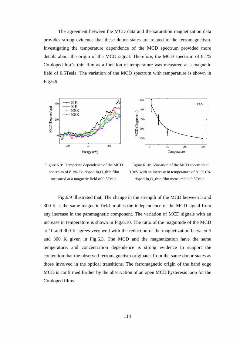
114
The agreement between the MCD data and the saturation magnetization data
provides strong evidence that these donor states are related to the ferromagnetism.
Investigating the temperature dependence of the MCD spectrum provided more
details about the origin of the MCD signal. Therefore, the MCD spectrum of 8.1%
Co-doped In2O3 thin film as a function of temperature was measured at a magnetic
field of 0.5Tesla. The variation of the MCD spectrum with temperature is shown in
Fig.6.9.
2.0 2.5 3.0
0
200
400
MCD
(Deg
rees
/cm)
Energy (eV)
10 K 50 K 100 K 300 K
0 100 200 300
250
300
350
400
450
MCD
(Deg
ree/c
m)
Temperature
3.3eV
Figure 6.9: Temperate dependence of the MCD
spectrum of 8.1% Co-doped In2O3 thin film
measured at a magnetic field of 0.5Tesla.
Figure 6.10: Variation of the MCD spectrum at
3.3eV with an increase in temperature of 8.1% Co-
doped In2O3 thin film measured at 0.5Tesla.
Fig.6.9 illustrated that, The change in the strength of the MCD between 5 and
300 K at the same magnetic field implies the independence of the MCD signal from
any increase in the paramagnetic component. The variation of MCD signals with an
increase in temperature is shown in Fig.6.10. The ratio of the magnitude of the MCD
at 10 and 300 K agrees very well with the reduction of the magnetization between 5
and 300 K given in Fig.6.3. The MCD and the magnetization have the same
temperature, and concentration dependence is strong evidence to support the
contention that the observed ferromagnetism originates from the same donor states as
those involved in the optical transitions. The ferromagnetic origin of the band edge
MCD is confirmed further by the observation of an open MCD hysteresis loop for the
Co-doped films.

115
Figure 6.11: Hysteresis loops for an 8.1% Co-doped In2O3 film using a SQUID magnetometer and
using MCD taken at 3.2 eV at room temperature. In both cases, the background signal from the
substrate was subtracted[17].
Fig.6.11 shows that, the MCD loop of an 8.1% Co-doped In2O3 sample was
superimposed upon a magnetic hysteresis loop for the same film measured using a
SQUID at room temperature. The shapes of the loops are very similar, and the
coercive fields are almost identical (inset, Fig. 6.11).
Ali films were deposited using sputtering system has no metallic Co while thin
films gown using PLD system containing an amount of metallic Co. Typical that film
characteristic is very sensitive to the exact conditions of fabrication.
In order to investigate the variation of optical and magneto-optical properties
of Co-doped In2O3 with oxygen partial pressure, annealing in vacuum process, and
doping with Tin, KACST engineers S. Alfahad and M. Alotibi deposited thin films of
(In1-x-yCoxSny)2O3 on sapphire (Al2O3) substrates using the PLD system. The data of
some representative thin films will be given. The annealed thin films were in a
vacuum for half an hour. The substrate temperature of these thin films was sustained
at 600 ˚C and the oxygen partial pressure was varied between 2x10⁻³ mTorr and
10mTorr. The growth details are shown in Table 6.2.
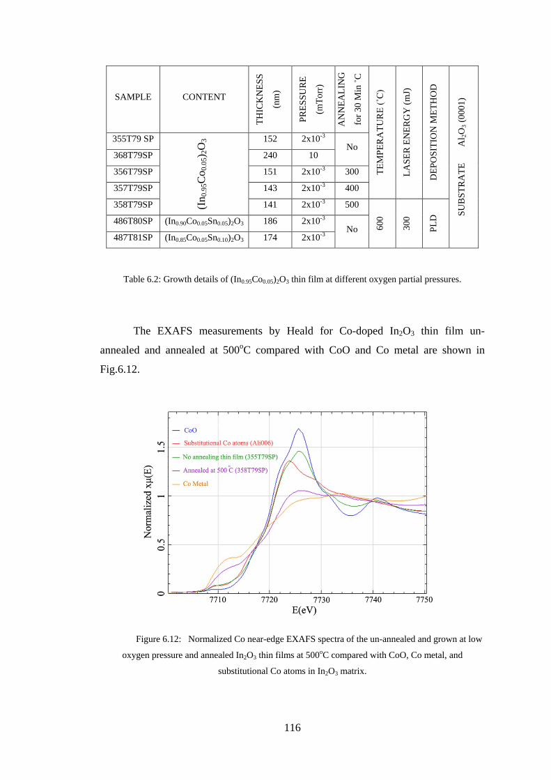
116
SAMPLE CONTENT
THIC
KN
ESS
(nm
)
PRES
SUR
E
(mTo
rr)
AN
NEA
LIN
G
for 3
0 M
in ˚C
TEM
PER
ATU
RE
(˚C
)
LASE
R E
NER
GY
(mJ)
DEP
OSI
TIO
N M
ETH
OD
SUB
STR
ATE
Al 2O
3 (00
01)
355T79 SP
(In 0
.95C
o 0.0
5)2O
3
152 2x10⁻³ No
368T79SP 240 10
356T79SP 151 2x10⁻³ 300
357T79SP 143 2x10⁻³ 400
358T79SP 141 2x10⁻³ 500
600
300
PLD
486T80SP (In0.90Co0.05Sn0.05)2O3 186 2x10⁻³ No
487T81SP (In0.85Co0.05Sn0.10)2O3 174 2x10⁻³
Table 6.2: Growth details of (In0.95Co0.05)2O3 thin film at different oxygen partial pressures.
The EXAFS measurements by Heald for Co-doped In2O3 thin film un-
annealed and annealed at 500oC compared with CoO and Co metal are shown in
Fig.6.12.
Figure 6.12: Normalized Co near-edge EXAFS spectra of the un-annealed and grown at low
oxygen pressure and annealed In2O3 thin films at 500oC compared with CoO, Co metal, and
substitutional Co atoms in In2O3 matrix.
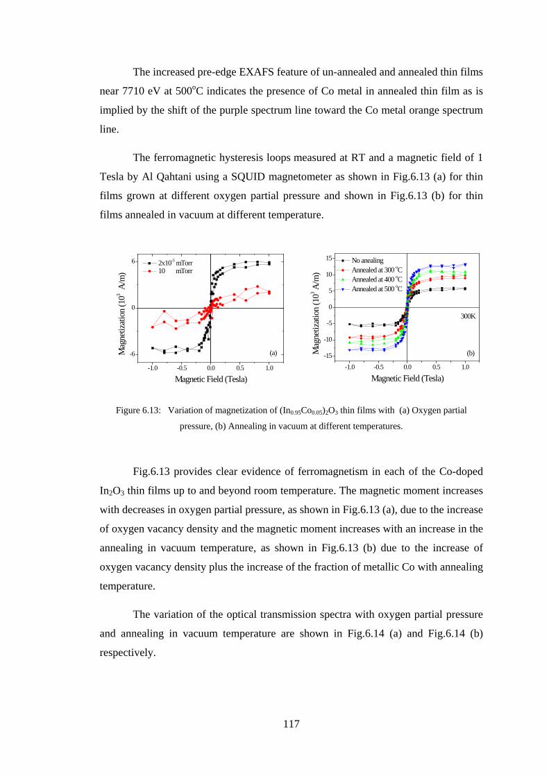
117
The increased pre-edge EXAFS feature of un-annealed and annealed thin films
near 7710 eV at 500oC indicates the presence of Co metal in annealed thin film as is
implied by the shift of the purple spectrum line toward the Co metal orange spectrum
line.
The ferromagnetic hysteresis loops measured at RT and a magnetic field of 1
Tesla by Al Qahtani using a SQUID magnetometer as shown in Fig.6.13 (a) for thin
films grown at different oxygen partial pressure and shown in Fig.6.13 (b) for thin
films annealed in vacuum at different temperature.
-1.0 -0.5 0.0 0.5 1.0
-6
0
6
Mag
netiz
ation
(103 A
/m)
Magnetic Field (Tesla)
2x10⁻³ mTorr 10 mTorr
(a)
-1.0 -0.5 0.0 0.5 1.0
-15
-10
-5
0
5
10
15
300K
No anealing Annealed at 300 oC Annealed at 400 oC Annealed at 500 oC
Mag
netiz
atio
n (1
03 A/m
)
Magnetic Field (Tesla)
(b)
Figure 6.13: Variation of magnetization of (In0.95Co0.05)2O3 thin films with (a) Oxygen partial
pressure, (b) Annealing in vacuum at different temperatures.
Fig.6.13 provides clear evidence of ferromagnetism in each of the Co-doped
In2O3 thin films up to and beyond room temperature. The magnetic moment increases
with decreases in oxygen partial pressure, as shown in Fig.6.13 (a), due to the increase
of oxygen vacancy density and the magnetic moment increases with an increase in the
annealing in vacuum temperature, as shown in Fig.6.13 (b) due to the increase of
oxygen vacancy density plus the increase of the fraction of metallic Co with annealing
temperature.
The variation of the optical transmission spectra with oxygen partial pressure
and annealing in vacuum temperature are shown in Fig.6.14 (a) and Fig.6.14 (b)
respectively.
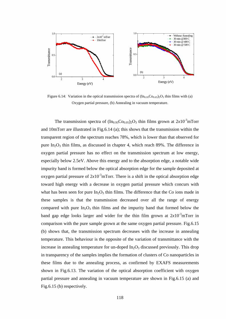
118
2 3 40.0
0.5
1.0
Tran
smitt
ance
Energy (eV)
2x10⁻³ mTorr 10mTorr
(a)
2 3 40.0
0.5
1.0
Tran
smitt
ance
Energy (eV)
Without Annealing 30 min @300 C 30 min @ 400 C 30 min @ 500 C
(b)
Figure 6.14: Variation in the optical transmission spectra of (In0.95Co0.05)2O3 thin films with (a)
Oxygen partial pressure, (b) Annealing in vacuum temperature.
The transmission spectra of (In0.95Co0.05)2O3 thin films grown at 2x10⁻³mTorr
and 10mTorr are illustrated in Fig.6.14 (a); this shows that the transmission within the
transparent region of the spectrum reaches 78%, which is lower than that observed for
pure In2O3 thin films, as discussed in chapter 4, which reach 89%. The difference in
oxygen partial pressure has no effect on the transmission spectrum at low energy,
especially below 2.5eV. Above this energy and to the absorption edge, a notable wide
impurity band is formed below the optical absorption edge for the sample deposited at
oxygen partial pressure of 2x10⁻³mTorr. There is a shift in the optical absorption edge
toward high energy with a decrease in oxygen partial pressure which concurs with
what has been seen for pure In2O3 thin films. The difference that the Co ions made in
these samples is that the transmission decreased over all the range of energy
compared with pure In2O3 thin films and the impurity band that formed below the
band gap edge looks larger and wider for the thin film grown at 2x10⁻³mTorr in
comparison with the pure sample grown at the same oxygen partial pressure. Fig.6.15
(b) shows that, the transmission spectrum decreases with the increase in annealing
temperature. This behaviour is the opposite of the variation of transmittance with the
increase in annealing temperature for un-doped In2O3 discussed previously. This drop
in transparency of the samples implies the formation of clusters of Co nanoparticles in
these films due to the annealing process, as confirmed by EXAFS measurements
shown in Fig.6.13. The variation of the optical absorption coefficient with oxygen
partial pressure and annealing in vacuum temperature are shown in Fig.6.15 (a) and
Fig.6.15 (b) respectively.

119
2 3 40
10
20
α (1
04 cm-1)
Energy (eV)
2x10⁻³ mTorr 10mTorr
(a)
2 3 40
10
20
(b)
α (1
04 cm-1)
Energy (eV)
Without Annealing 30 min @300 oC 30 min @ 400 oC 30 min @ 500 oC
Figure 6.15: Variation in the optical absorption coefficient of (In0.95Co0.05)2O3 with (a) Oxygen partial
pressure, (b) Annealing in vacuum temperature.
Fig.6.15 (a) shows two absorption features seen at 2.3eV and 3.3eV in both
samples. The feature at 2.3eV did not exist before in the optical absorption spectrum
of pure In2O3 discussed in chapter 4, which means that this feature is related to the
TM-doped material (cobalt). In fact, the feature at 2.3eV implies the formation of Co
nanoparticles in both thin films and the density of the Co nanoparticles is greater in
the sample deposited at base pressure; this explains the high and wide absorption seen
at this energy. The source of these peaks can be explored in greater depth though the
magneto-optical measurement. Fig.6.15 (b) shows that, the optical absorption
coefficient is annealing-temperature dependent. The absorption spectra show
continuous transitions from 1.8eV to around 3.9eV where the band gap is. These
continuous transitions are due to the formation of defect bands below the band gap
energy and due to the contribution of metallic Co. The variation in the absorption
coefficient squared and the optical band gap with oxygen partial pressure and
annealing in vacuum temperature are shown in Fig.6.16 (a) and Fig.6.16 (b)
respectively.

120
2 3 40
50
100
(αhν
)2 x10¹⁰
(eV/
cm)2
Energy (eV)
2x10⁻³ mTorr 10mTorr
(a)
2 3 40
20
40
60
Non 300 400 5003.75
3.80
3.85
3.90
3.95
4.00
Eg (e
V)
annealing for 30 Min at (c)
(αhν
)2 x10¹⁰
(eV/
cm)2
Energy (eV)
Without annealing 30 min @ 300 C 30 min @ 400 C 30 min @ 500 C
(b)
Figure 6.16 : Variation in the optical band gap energy of (In0.95Co0.05)2O3 thin films with (a) oxygen
partial pressure, (b) Annealing in vacuum temperature.
Fig.6.16 (a) shows that, the optical band gap energy of (In0.95Co0.05)2O3 thin
films increases with decreases in oxygen partial pressure. The same behaviour was
observed in pure In2O3 thin films, and doping In2O3 with up to 5% of cobalt has no
effect on the variation of the optical band gap of In2O3 semiconductor with oxygen
partial pressure. Fig.6.16 (b) shows that, the optical band gap energy is annealing-
temperature independent within the error range, which indicates that these thin films
had been grown with very high crystallization, and no enhancement occurs due to the
annealing process. It is expected that the optical band gap energy will shift toward
higher energy as seen before for pure In2O3, but in annealed (In0.95Co0.05)2O3 thin
films, the carrier density seems to decrease with the annealing process due to the Co
doping. The MCD spectrum of (In0.95Co0.05)2O3 thin films are shown in Fig.6.17.
1.5 2.0 2.5 3.0 3.5
-1000
0
1000
MCD
(a.u
/cm)
Energy (eV)
2x10⁻³ mTorr 10 mTorr
(a)
1.5 2.0 2.5 3.0 3.5-2000
-1000
0
1000
2000
MCD
(Deg
ree/c
m)
Energy (eV)
without annealing Annealed at 300 oC Annealed at 400 oC Annealed at 500 oC
(b)
Figure 6.17 : Variation in MCD spectrum of (In0.95Co0.05)2O3 thin films with (a) oxygen partial
pressure, (b) Annealing in vacuum temperature.
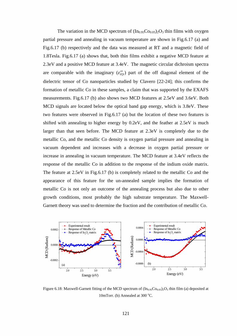
121
The variation in the MCD spectrum of (In0.95Co0.05)2O3 thin films with oxygen
partial pressure and annealing in vacuum temperature are shown in Fig.6.17 (a) and
Fig.6.17 (b) respectively and the data was measured at RT and a magnetic field of
1.8Tesla. Fig.6.17 (a) shows that, both thin films exhibit a negative MCD feature at
2.3eV and a positive MCD feature at 3.4eV. The magnetic circular dichroism spectra
are comparable with the imaginary (𝜀𝑥𝑦′′ ) part of the off diagonal element of the
dielectric tensor of Co nanoparticles studied by Clavero [22-24]; this confirms the
formation of metallic Co in these samples, a claim that was supported by the EXAFS
measurements. Fig.6.17 (b) also shows two MCD features at 2.5eV and 3.6eV. Both
MCD signals are located below the optical band gap energy, which is 3.8eV. These
two features were observed in Fig.6.17 (a) but the location of these two features is
shifted with annealing to higher energy by 0.2eV, and the feather at 2.5eV is much
larger than that seen before. The MCD feature at 2.3eV is completely due to the
metallic Co, and the metallic Co density is oxygen partial pressure and annealing in
vacuum dependent and increases with a decrease in oxygen partial pressure or
increase in annealing in vacuum temperature. The MCD feature at 3.4eV reflects the
response of the metallic Co in addition to the response of the indium oxide matrix.
The feature at 2.5eV in Fig.6.17 (b) is completely related to the metallic Co and the
appearance of this feature for the un-annealed sample implies the formation of
metallic Co is not only an outcome of the annealing process but also due to other
growth conditions, most probably the high substrate temperature. The Maxwell-
Garnett theory was used to determine the fraction and the contribution of metallic Co.
2.0 2.5 3.0 3.5
-0.0002
0.0000
0.0002 Experimental result Response of Metallic Co Response of In2O3 matrix
MCD
(Rad
ians)
Energy (eV)
(a)
2.0 2.5 3.0 3.5
-0.0008
-0.0004
0.0000
0.0004
MCD
(Rad
ians)
Energy (eV)
Experimental result Response of Metallic Co Response of In2O3 matrix
(b)
Figure 6.18: Maxwell-Garnett fitting of the MCD spectrum of (In0.95Co0.05)2O3 thin film (a) deposited at
10mTorr. (b) Annealed at 300 oC.
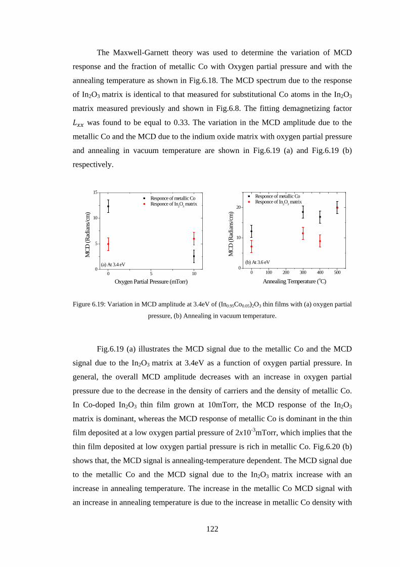
122
The Maxwell-Garnett theory was used to determine the variation of MCD
response and the fraction of metallic Co with Oxygen partial pressure and with the
annealing temperature as shown in Fig.6.18. The MCD spectrum due to the response
of In2O3 matrix is identical to that measured for substitutional Co atoms in the In2O3
matrix measured previously and shown in Fig.6.8. The fitting demagnetizing factor
𝐿𝑥𝑥 was found to be equal to 0.33. The variation in the MCD amplitude due to the
metallic Co and the MCD due to the indium oxide matrix with oxygen partial pressure
and annealing in vacuum temperature are shown in Fig.6.19 (a) and Fig.6.19 (b)
respectively.
0 5 100
5
10
15
Responce of metallic Co Responce of In2O3 matrix
MCD
(Rad
ians
/cm
)
Oxygen Partial Pressure (mTorr)
(a) At 3.4 eV
0 100 200 300 400 5000
10
20
MCD
(Rad
ians/c
m)
Annealing Temperature (oC)
Responce of metallic Co Responce of In2O3 matrix
(b) At 3.6 eV
Figure 6.19: Variation in MCD amplitude at 3.4eV of (In0.95Co0.05)2O3 thin films with (a) oxygen partial
pressure, (b) Annealing in vacuum temperature.
Fig.6.19 (a) illustrates the MCD signal due to the metallic Co and the MCD
signal due to the In2O3 matrix at 3.4eV as a function of oxygen partial pressure. In
general, the overall MCD amplitude decreases with an increase in oxygen partial
pressure due to the decrease in the density of carriers and the density of metallic Co.
In Co-doped In2O3 thin film grown at 10mTorr, the MCD response of the In2O3
matrix is dominant, whereas the MCD response of metallic Co is dominant in the thin
film deposited at a low oxygen partial pressure of 2x10⁻³mTorr, which implies that the
thin film deposited at low oxygen partial pressure is rich in metallic Co. Fig.6.20 (b)
shows that, the MCD signal is annealing-temperature dependent. The MCD signal due
to the metallic Co and the MCD signal due to the In2O3 matrix increase with an
increase in annealing temperature. The increase in the metallic Co MCD signal with
an increase in annealing temperature is due to the increase in metallic Co density with
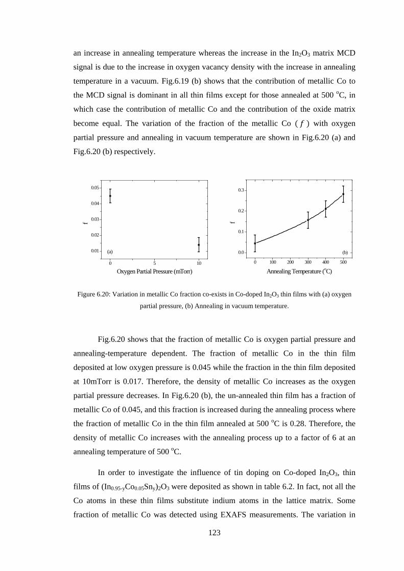
123
an increase in annealing temperature whereas the increase in the In2O3 matrix MCD
signal is due to the increase in oxygen vacancy density with the increase in annealing
temperature in a vacuum. Fig.6.19 (b) shows that the contribution of metallic Co to
the MCD signal is dominant in all thin films except for those annealed at 500 oC, in
which case the contribution of metallic Co and the contribution of the oxide matrix
become equal. The variation of the fraction of the metallic Co ( 𝑓 ) with oxygen
partial pressure and annealing in vacuum temperature are shown in Fig.6.20 (a) and
Fig.6.20 (b) respectively.
0 5 10
0.01
0.02
0.03
0.04
0.05
f
Oxygen Partial Pressure (mTorr)
(a)
0 100 200 300 400 500
0.0
0.1
0.2
0.3
f
Annealing Temperature (oC)
(b)
Figure 6.20: Variation in metallic Co fraction co-exists in Co-doped In2O3 thin films with (a) oxygen
partial pressure, (b) Annealing in vacuum temperature.
Fig.6.20 shows that the fraction of metallic Co is oxygen partial pressure and
annealing-temperature dependent. The fraction of metallic Co in the thin film
deposited at low oxygen pressure is 0.045 while the fraction in the thin film deposited
at 10mTorr is 0.017. Therefore, the density of metallic Co increases as the oxygen
partial pressure decreases. In Fig.6.20 (b), the un-annealed thin film has a fraction of
metallic Co of 0.045, and this fraction is increased during the annealing process where
the fraction of metallic Co in the thin film annealed at 500 oC is 0.28. Therefore, the
density of metallic Co increases with the annealing process up to a factor of 6 at an
annealing temperature of 500 oC.
In order to investigate the influence of tin doping on Co-doped In2O3, thin
films of (In0.95-yCo0.05Sny)2O3 were deposited as shown in table 6.2. In fact, not all the
Co atoms in these thin films substitute indium atoms in the lattice matrix. Some
fraction of metallic Co was detected using EXAFS measurements. The variation in

124
the optical transmission and reflection of (In0.95-yCo0.05Sny)2O3 thin films with tin
content is shown in Fig.6.21.
2 3 40.0
0.5
1.0
Tr
ansm
ittan
ce
Energy (eV)
0% Sn 5% Sn 10% Sn
2 3 40.0
0.5
1.0
Refle
ction
Energy (eV)
0% Sn 5% Sn 10% Sn
Figure 6.21: Variation in the optical transmission and reflection of (In0.95-yCo0.05Sny)2O3 thin films with
tin content, where metallic Co in these thin film is detected.
The transmission increases with an increase in tin content, which is in
agreement with the same result obtained for the pure In2O3 thin films discussed in
chapter 4. The optical absorption edge is shifted toward higher energy with an
increase in tin content of up to 5% of tin; then, the optical absorption edge is shifted
toward low energy due to the un-embedded tin atoms of tin in the In2O3 lattice where
the density of un-embedded tin atoms increases with an increase in tin content of
more than 5%. The transmission at 550nm and the optical absorption coefficient
spectra as a function of tin content are shown in Fig.6.22.
0 5 100.76
0.78
0.80
0.82
Tran
smitt
ance
(at 5
50nm
)
Sn Content (%)
2 3 40
5
10
15
α (1
04 cm-1)
Energy (eV)
0% Sn 5% Sn 10% Sn
Figure 6.22: Variation in the optical transmission at 550nm, 2.3eV, and the optical absorption
coefficient of (In0.95-yCo0.05Sny)2O3 thin films with tin content.

125
The absorption coefficient spectra of un-doped-with-tin thin film show two
transitions, the first at 2.4eV and the second below the optical absorption edge at
3.5eV. The first transition, at 2.4eV, is due to the metallic Co. This transition feature
disappears when the thin film is doped with tin. The thin films doped with tin show
just one transition feature at 3.4eV and the behaviour of the optical absorption edge
with tin is in agreement with what was observed in the transmission spectra, as shown
in Fig.6.21. The absorption coefficient is non-zero at 3.3eV and increases with an
increase in energy up to the absorption band edge. The area between 3.3eV and the
optical band gap energy is where the energy states of defects are formed. Therefore, it
is obvious that the formation of energy states by defects increases with an increase in
tin content. Increasing tin content leads to a shift of the optical absorption coefficient
spectrum toward high energy. When the doping with tin is increased to above 5%, the
interstitial Sn atoms in the lattice start to exist; this, in turn, causes the shift in
absorption of the coefficient spectra toward low energy. The variation of the optical
absorption coefficient squared and the optical band gap with tin content are shown in
Fig.6.23.
2 3 40
25
50
(αhν
)2 x10¹⁰
(eV
/cm
)2
Energy (eV)
0% Sn 5% Sn 10% Sn
0 5 10
3.8
4.0
4.2
Eg (e
V)
Sn Content (%)
Figure 6.23: Variation in the optical absorption coefficient squared and the optical band gap with tin
content of (In0.95-yCo0.05Sny)2O3 thin films.
Fig.6.23 shows that, the optical band gap energy of (In0.95-yCo0.05Sny)2O3 thin
films is tin-content dependent. The optical band gap energy increases with an increase
in tin content of up to 5% then it decreases afterwards, confirming that with more than
5% of tin, the tin atoms are not soluble in the lattice, which affects all the optical
properties of these thin films. The increase in the optical band gap energy is due to the
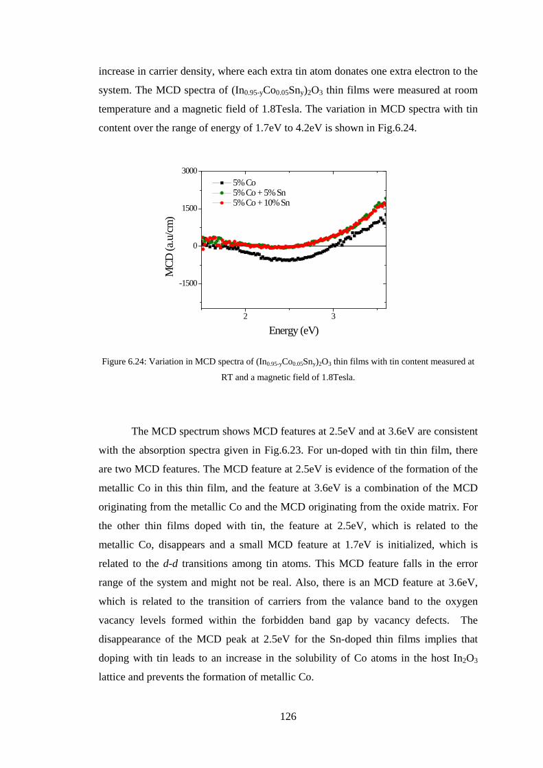
126
increase in carrier density, where each extra tin atom donates one extra electron to the
system. The MCD spectra of (In0.95-yCo0.05Sny)2O3 thin films were measured at room
temperature and a magnetic field of 1.8Tesla. The variation in MCD spectra with tin
content over the range of energy of 1.7eV to 4.2eV is shown in Fig.6.24.
2 3
-1500
0
1500
3000
M
CD (a
.u/cm
)
Energy (eV)
5% Co 5% Co + 5% Sn 5% Co + 10% Sn
Figure 6.24: Variation in MCD spectra of (In0.95-yCo0.05Sny)2O3 thin films with tin content measured at
RT and a magnetic field of 1.8Tesla.
The MCD spectrum shows MCD features at 2.5eV and at 3.6eV are consistent
with the absorption spectra given in Fig.6.23. For un-doped with tin thin film, there
are two MCD features. The MCD feature at 2.5eV is evidence of the formation of the
metallic Co in this thin film, and the feature at 3.6eV is a combination of the MCD
originating from the metallic Co and the MCD originating from the oxide matrix. For
the other thin films doped with tin, the feature at 2.5eV, which is related to the
metallic Co, disappears and a small MCD feature at 1.7eV is initialized, which is
related to the d-d transitions among tin atoms. This MCD feature falls in the error
range of the system and might not be real. Also, there is an MCD feature at 3.6eV,
which is related to the transition of carriers from the valance band to the oxygen
vacancy levels formed within the forbidden band gap by vacancy defects. The
disappearance of the MCD peak at 2.5eV for the Sn-doped thin films implies that
doping with tin leads to an increase in the solubility of Co atoms in the host In2O3
lattice and prevents the formation of metallic Co.

127
6.3 Conclusion This chapter investigated the influence of Co-doping on the optical and
magneto-optical properties of In2O3 thin films. The results provide compelling
evidence that the observed ferromagnetism in SMS is due to the polarized electrons in
localized donor states associated with the oxygen vacancies. Magnetometry and
magneto-optical measurements show that Co-doped In2O3 is ferromagnetic beyond
room temperature. The density of impurity donor states formed below the band gap
edge is due to the oxygen vacancies and increases and widens with decreases in
oxygen partial pressure, with an increase in Co content, and with doping with Sn as
confirmed by magneto-optical measurements.
EXAFS measurements confirmed that some thin films contain metallic Co
nanoparticles. Therefore, the magnetization and the magneto-optics’ behaviours will
be a mix of that due to the response of metallic Co and that due to the response of the
semiconductor matrix. However, the EXAFS measurements could not give the
fraction of these nanoparticles. Magneto-optical measurements were found to be more
accurate and quantitative in this field.
The fraction and the MCD response of metallic Co that co-exist in some thin
films and the MCD response of In2O3 matrix were found to increase with a decrease in
the oxygen partial pressure or with an increase in the annealing temperature in a
vacuum. The vacuum annealing process improves the magnetization, the magneto-
optical responses of metallic Co and the In2O3 matrix.
Although the oxygen partial pressure and the annealing process lead to an
increase in the fraction of metallic Co, there is no evidence that the oxygen partial
pressure or the annealing process is responsible for the existence of metallic Co in
these thin films where the metallic Co is observed in thin films deposited at high
oxygen partial pressure and in un-annealed thin films. Therefore, the responsibility for
the existence of metallic Co is most likely to be the substrate temperature, which is as
high as 600oC in all thin films containing metallic Co, or due to the high laser power
used to prepare the thin films.
Doping with tin up to 5% increases the transparency and the carrier
concentration of the samples whereas doping with a fraction of tin of more than 5%

128
leads the interstitial Sn ions to form and act as scattering centres. The amplitude of the
MCD signal is in accordance with the carrier density and the density of the oxygen
vacancy bands, which implies that the carrier density and the impurity donor states are
responsible for the observed MCD signal and the transitions within the forbidden
band gap energy. The metallic Co does not appears in Sn-doped thin films, indicating
that doping with tin leads to an increase in the solubility of Co atoms in the host In2O3
lattice and prevents the formation of metallic Co.
129
6.4 References 1. N. H. Hong, J. Sakai, W. Prellier and A. Hassini , J. Phys. : Condens. Matter
17, 1697 (2005).
2. J. M. D. Coey, A. P. Douvalis, C. B. Fitzgerald and M. Venkatesan, Appl.
Phys. Lett. 84, 1332-1334 (2004).
3. S. B. Ogale, R. J. Choudhary, J. P. Buban, S. E. Lofland, S. R. Shinde, S. N.
Kale, V. N. Kulkarni, J. Higgins, C. Lanci, J. R. Simpson, N. D. Browning, S.
D. Sarma, H. D. Drew, R. L. Greene and T. Venkatesan, Phys. Rev. Lett. 91,
077205 (2003).
4. M. Venkatesan, C. B. Fitzgerald, J. G. Lunney and J. M. D. Coey, Phys. Rev.
Lett. 93, 177206 (2004).
5. N. H. Hong, J. Sakai, W. Prellier, A. Hassini, A. Ruyter and F. Gervais, Phys.
Rev. B 70, 195204 (2004).
6. Z. Wang, J. Tang, L. D. Tung, W. Zhou and L. Spinu, J. Appl. Phys. 93, 7870-
7872 (2003).
7. G. Peleckis, X. L. Wang and S. X. Dou, J. Magn. Magn. Mater. 301, 308-311
(2006).
8. P. F. Xing, C. Y. Xue, T. M. Jian, Y. S. Shen, L. G. Lei, M. L. Mo and J. Jun,
Chinese Physics Letters 26, 117503 (2009).
9. X. Meng, L. Tang and J. Li, J. Phys. Chem. C 114, 17569-17573 (2010).
10. G. Peleckis, X. Wang and S. X. Dou, Appl. Phys. Lett. 89, 022501 (2006).
11. T. Dietl, H. Ohno and F. Matsukura, Phys. Rev. B 63, 195205 (2001).
12. T. Dietl, A. Haury and Y. D. A. Merle, Phys. Rev. B 55, R3347 (1997).
13. H. Akai, Phys. Rev. Lett. 81, 3002 (1998).
14. P. G. D. Gennes, Phys. Rev. 118, 141 (1960).
15. M. V. Schilfgaarde, and O. N. Mryasov, Phys. Rev. B 63, 233205 (2001).
16. P. W. Anderson, and H. Hasegawa, Phys. Rev. 100, 675 (1955).
17. A. M. H. R. Hakimi, M. G. Blamire, S. M. Heald, M. S. Alshammari, M. S.
Alqahtani, D. S. Score, H. J. Blythe, A. M. Fox and G. A. Gehring, Phys. Rev.
B 84, 085201 (2011).
18. D. S. Score, M. Alshammari, Q. Feng, H. J. Blythe, A. M. Fox,
G. A. Gehring, Z. Y. Quan, X. L. Li and X. H. Xu, J. Phys. : Conference
Series 200, 062024 (2010).
130
19. G. A. Gehring, H. J. Blythe, F. Qi, D. S. Score, A. Mokhtari, M. Alshammari,
M. S. Al Qahtani and A. M. Fox, Magnetics, IEEE Transactions on 46, 1784-
1786 (2010).
20. C. Clavero, A. Cebollada, G. Armelles, Y. Huttel, J. Arbiol, F. Peiró and A.
Cornet, Phys. Rev. B 72, 024441 (2005).
21. M. A. White, S. T. Ochsenbein and D. R. Gamelin, Chem. Mater. 20, 7107-
7116 (2008).
22. A. G. Clavero, J. Margueritat, J. Gonzalo, M. G. D. Muro, A. Labarta and B.
X, Appl. Phys. Lett. 90, 182506 (2007).
23. C.A. Clavero, G. Armelles, Y. Huttel, J. Arbiol, F. Peiró and A. Cornet, Phys
Rev 72, 02441 (2005).
24. C. Clavero, B. Sepúlveda, G. Armelles, Z. Konstantinović, M. García del
Muro, A. Labarta, and X. Batlle, J. Appl. Phys. 100, 074320 (2006).
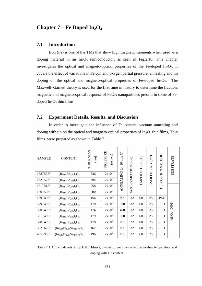
131
Chapter 7 – Fe Doped In2O3
7.1 Introduction Iron (Fe) is one of the TMs that show high magnetic moments when used as a
doping material in an In2O3 semiconductor, as seen in Fig.2.16. This chapter
investigates the optical and magneto-optical properties of the Fe-doped In2O3. It
covers the effect of variations in Fe content, oxygen partial pressure, annealing and tin
doping on the optical and magneto-optical properties of Fe-doped In2O3. The
Maxwell–Garnett theory is used for the first time in history to determine the fraction,
magnetic and magneto-optical response of Fe3O4 nanoparticles present in some of Fe-
doped In2O3 thin films.
7.2 Experiment Details, Results, and Discussion In order to investigate the influence of Fe content, vacuum annealing and
doping with tin on the optical and magneto-optical properties of In2O3 thin films, Thin
films were prepared as shown in Table 7.1.
SAMPLE CONTENT
THIC
KN
ESS
(nm
)
PRES
SUR
E
(mTo
rr)
AN
NEA
LIN
G fo
r 30
min
C˚
T&S
SEPA
RA
TIO
N (m
m)
TEM
PER
ATU
RE
(˚C
)
LASE
R E
NER
GY
(mJ)
DEP
OSI
TIO
N M
ETH
OD
SUB
STR
ATE
133T53SP (In0.99Fe0.01)2O3 336 2x10⁻³ 132T52SP (In0.98Fe0.02)2O3 294 2x10⁻³ 131T51SP (In0.97Fe0.03)2O3 258 2x10⁻³
Al 2O
3 (0
001)
130T50SP (In0.96Fe0.04)2O3 200 2x10⁻³ 129T49SP (In0.95Fe0.05)2O3 156 2x10⁻³ No 32 600 250 PLD
329T49SP (In0.95Fe0.05)2O3 170 2x10⁻³ 500 32 600 250 PLD 330T49SP (In0.95Fe0.05)2O3 174 2x10⁻³ 400 32 600 250 PLD 331T49SP (In0.95Fe0.05)2O3 179 2x10⁻³ 300 32 600 250 PLD 328T49SP (In0.95Fe0.05)2O3 178 2x10⁻³ No 32 600 250 PLD 362T62SP (In0.90Fe0.05Sn0.05)2O3 162 2x10⁻³ No 32 600 250 PLD 435T93SP (In0.85Fe0.05Sn0.10)2O3 196 2x10⁻³ No 32 600 250 PLD
Table 7.1: Growth details of In2O3 thin films grown at different Fe content, annealing temperature, and
doping with Tin content.

132
Thin films of (In1-x-yFexSny)2O3 with different concentrations of Fe3O4 varying
from 1% to 5%, and different concentrations of Sn were prepared by S. Alfahad and
M. Alotibi from the National Center of Nanotechnology at KACST. The oxygen
partial pressure was sustained at 2x10⁻³ mTorr during the growth process. The
influence of oxygen partial pressure will be investigated separately where the related
thin films grown in China not in KACST.
Starting with the influence of the Fe content, the XRD analysis by Hakimi
shows that, the thin films are very crystalline, prefer IO(222) orientation and the
Fe3O4 nanoparticles were also present.
20 30 40 50 60 70 80
Al2O3 (006)
IO (444)IO (321)
130 (4% Fe) 131 (3% Fe) 132 (2% Fe) 133 (1% Fe)
Inte
nsity
(Cou
nts)
2 θ (degrees)
IO (222)
Figure 7.1: XRD data of (In1-xFex)2O3 thin films where In2O3 (222) and (444) reflection peaks do not
shift with Fe concentrations, implying that not all Fe ions are substitutional.
20 30 40 50 60 70 80
Fe3O4 (333)
IO (400)
Al2O3 (006)
IO (444)
IO (321)
130 (4% Fe) 131 (3% Fe) 132 (2% Fe) 133 (1% Fe)
Ln in
tens
ity (C
ount
s)
2 θ (degrees)
IO (222)
(a)
56.25 56.50 56.75 57.00 57.25 57.50
Fe3O4 (333) 130 (4% Fe) 131 (3% Fe) 132 (2% Fe) 133 (1% Fe)
Inten
sity
(Cou
nts)
2 θ (degrees)
(b)
Figure 7.2: a) High resolution XRD data of (In1-xFex)2O3 thin films where Fe3O4 nanoparticles can be
seen. b) High resolution XRD data in the range from 56 to 57, which confirm the existence of Fe3O4
nanoparticles in all the thin films; its fraction increases with Fe-doping content.

133
The lattice constant fluctuates as shown in Fig.7.3, and does not show any
strong dependence on the level of Fe doping, which suggests that the Fe is not doping
substitutionally.
1.0 1.5 2.0 2.5 3.0 3.5 4.0
10.116
10.118
10.120
10.122
10.124
10.126
Latti
ce p
aram
eter
, a (A
)
Fe doping level, (%)
Figure 7.3: Fluctuation of the lattice constant with an increase in Fe content.
The EXAFS measurements performed by Heald on In2O3 thin film doped with
5% Fe compared with magnetite (Fe3O4) are shown in Fig.7.4.
Figure 7.4: Normalized Fe near-edge EXAFS spectra of the In2O3 thin film doped with 4%
Fe compared with Fe3O4.
The EXAFS measurements confirmed the formation of nanoparticles of
magnetite in the In2O3 thin films. Variation of the resistance with temperature is
shown in Fig.7.5
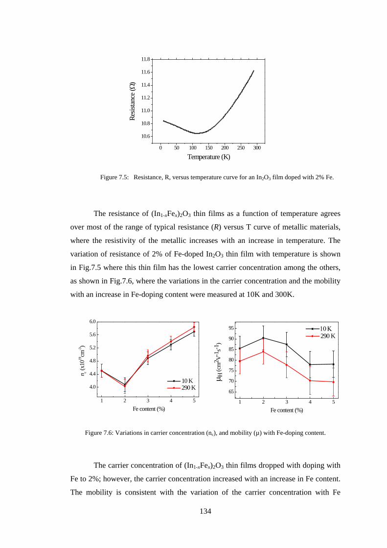
134
0 50 100 150 200 250 300
10.6
10.8
11.0
11.2
11.4
11.6
11.8
Resis
tanc
e (Ω
)
Temperature (K)
Figure 7.5: Resistance, R, versus temperature curve for an In2O3 film doped with 2% Fe.
The resistance of (In1-xFex)2O3 thin films as a function of temperature agrees
over most of the range of typical resistance (R) versus T curve of metallic materials,
where the resistivity of the metallic increases with an increase in temperature. The
variation of resistance of 2% of Fe-doped In2O3 thin film with temperature is shown
in Fig.7.5 where this thin film has the lowest carrier concentration among the others,
as shown in Fig.7.6, where the variations in the carrier concentration and the mobility
with an increase in Fe-doping content were measured at 10K and 300K.
1 2 3 4 5
4.0
4.4
4.8
5.2
5.6
6.0
Fe content (%)
10 K 290 K
n c (x10
19cm
-3)
1 2 3 4 5
65
70
75
80
85
90
95
10 Κ 290 K
µ H (c
m2 V
-1s-1
)
Fe content (%)
Figure 7.6: Variations in carrier concentration (nc), and mobility (µ) with Fe-doping content.
The carrier concentration of (In1-xFex)2O3 thin films dropped with doping with
Fe to 2%; however, the carrier concentration increased with an increase in Fe content.
The mobility is consistent with the variation of the carrier concentration with Fe

135
content until it is saturated above 4% of Fe content. Magnetic properties were
investigated using a SQUID magnetometer in the temperature range of 5–300 K in
magnetic fields up to 1 Tesla. Variation of magnetic moment with applied magnetic
field displayed ferromagnetism in each of the Fe-doped In2O3 films above room
temperature due to the formation of Fe3O4 nanoparticles as shown in Fig.7.7.
-1.0 -0.5 0.0 0.5 1.0-30
-20
-10
0
10
20
30
0.0
-20
-10
0
10
20
Mag
netiz
atio
n(10
3 A/m
)
Magnetic Field (Tesla)
Mag
netiz
ation
(103 A
/m)
Magnetic Field (Tesla)
1% Fe 2% Fe 3% Fe 4% Fe 5% Fe
5K
(a)
-1.0 -0.5 0.0 0.5 1.0-30
-20
-10
0
10
20
30
0.0
-20
-10
0
10
20
Mag
netiz
atio
n (1
03 A/m
)
Magnetic Field (Tesla)
5K 300K
(b)
Mag
netiz
atio
n (1
03 A/m
)Magnetic Field (Tesla)
5K 300K
5% Fe
(b)
Figure 7.7: a) Ferromagnetic hysteresis loops of a Fe-doped In2O3 thin film at 5 K.
b) Hysteresis loops of 5% Fe-doped In2O3 thin film at 5K and 300K.
The magnetization increases with an increase in Fe content and in agreement
with the carrier concentration, as shown in Fig.7.6 except that 2% of Fe thin film
shows a higher magnetization than that of 1% thin film, while the carrier
concentration of 2% thin film is lower than that of 1%, which was not expected due to
correlation between the magnetization and the carrier concentration. The optical
transmission and optical reflection spectrum of (In1-xFex)2O3 thin films as a function
of energy were measured at RT and are shown in Fig.7.8.
Tran
smitt
ance
2.0 2.5 3.0 3.5 4.0 4.50.00.10.20.30.40.50.60.70.80.91.0
5%
Energy (eV)
1% Fe 2% Fe 3% Fe 4% Fe 5% Fe Ts 1%
2.0 2.5 3.0 3.5 4.0 4.50.10
0.15
0.20
0.25
0.30
0.35
Refle
ctan
ce (%
)
Energy (eV)
1% Fe 2% Fe 3% Fe 4% Fe 5% Fe
Figure 7.8: Variation in the optical transmission, and reflection spectrum with Fe ions content.
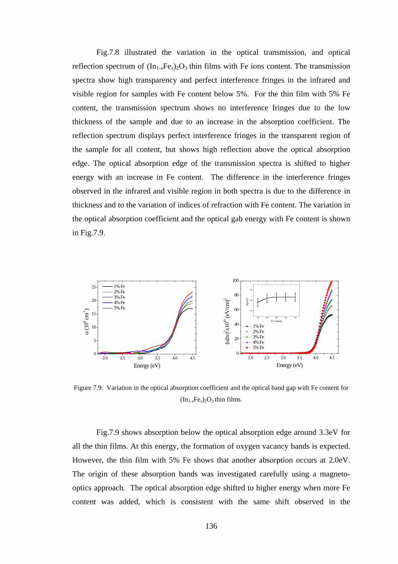
136
Fig.7.8 illustrated the variation in the optical transmission, and optical
reflection spectrum of (In1-xFex)2O3 thin films with Fe ions content. The transmission
spectra show high transparency and perfect interference fringes in the infrared and
visible region for samples with Fe content below 5%. For the thin film with 5% Fe
content, the transmission spectrum shows no interference fringes due to the low
thickness of the sample and due to an increase in the absorption coefficient. The
reflection spectrum displays perfect interference fringes in the transparent region of
the sample for all content, but shows high reflection above the optical absorption
edge. The optical absorption edge of the transmission spectra is shifted to higher
energy with an increase in Fe content. The difference in the interference fringes
observed in the infrared and visible region in both spectra is due to the difference in
thickness and to the variation of indices of refraction with Fe content. The variation in
the optical absorption coefficient and the optical gab energy with Fe content is shown
in Fig.7.9.
2.0 2.5 3.0 3.5 4.0 4.50
5
10
15
20
25
α (1
04 cm-1)
Energy (eV)
1% Fe 2% Fe 3% Fe 4% Fe 5% Fe
2.0 2.5 3.0 3.5 4.0 4.50
20
40
60
80
100
1% 2% 3% 4% 5%
3.8
3.9
4.0
Eg (e
V)
Fe Content
(αhν
)2 x10¹⁰
(eV/
cm)2
Energy (eV)
1% Fe 2% Fe 3% Fe 4% Fe 5% Fe
Figure 7.9: Variation in the optical absorption coefficient and the optical band gap with Fe content for
(In1-xFex)2O3 thin films.
Fig.7.9 shows absorption below the optical absorption edge around 3.3eV for
all the thin films. At this energy, the formation of oxygen vacancy bands is expected.
However, the thin film with 5% Fe shows that another absorption occurs at 2.0eV.
The origin of these absorption bands was investigated carefully using a magneto-
optics approach. The optical absorption edge shifted to higher energy when more Fe
content was added, which is consistent with the same shift observed in the
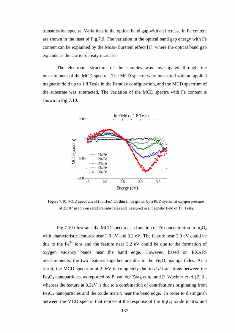
137
transmission spectra. Variations in the optical band gap with an increase in Fe content
are shown in the inset of Fig.7.9. The variation in the optical band gap energy with Fe
content can be explained by the Moss–Burstein effect [1], where the optical band gap
expands as the carrier density increases.
The electronic structure of the samples was investigated through the
measurement of the MCD spectra. The MCD spectra were measured with an applied
magnetic field up to 1.8 Tesla in the Faraday configuration, and the MCD spectrum of
the substrate was subtracted. The variation of the MCD spectra with Fe content is
shown in Fig.7.10.
1.5 2.0 2.5 3.0 3.5-2000
-1000
0
1000
MCD
(a.u
/cm)
Energy (eV)
1% Fe 2% Fe 3% Fe 4% Fe 5% Fe
In Field of 1.8 Tesla
Figure 7.10: MCD spectrum of (In1-xFex)2O3 thin films grown by a PLD system at oxygen pressure
of 2x10⁻⁶ mTorr on sapphire substrates and measured in a magnetic field of 1.8 Tesla.
Fig.7.10 illustrates the MCD spectra as a function of Fe concentration in In2O3
with characteristic features near 2.0 eV and 3.2 eV. The feature near 2.0 eV could be
due to the Fe2+ ions and the feature near 3.2 eV could be due to the formation of
oxygen vacancy bands near the band edge. However, based on EXAFS
measurements, the two features together are due to the Fe3O4 nanoparticles. As a
result, the MCD spectrum at 2.0eV is completely due to d-d transitions between the
Fe3O4 nanoparticles, as reported by P. van der Zaag et al. and P. Wachter et al. [2, 3],
whereas the feature at 3.2eV is due to a combination of contributions originating from
Fe3O4 nanoparticles and the oxide matrix near the band edge. In order to distinguish
between the MCD spectra that represent the response of the In2O3 oxide matrix and
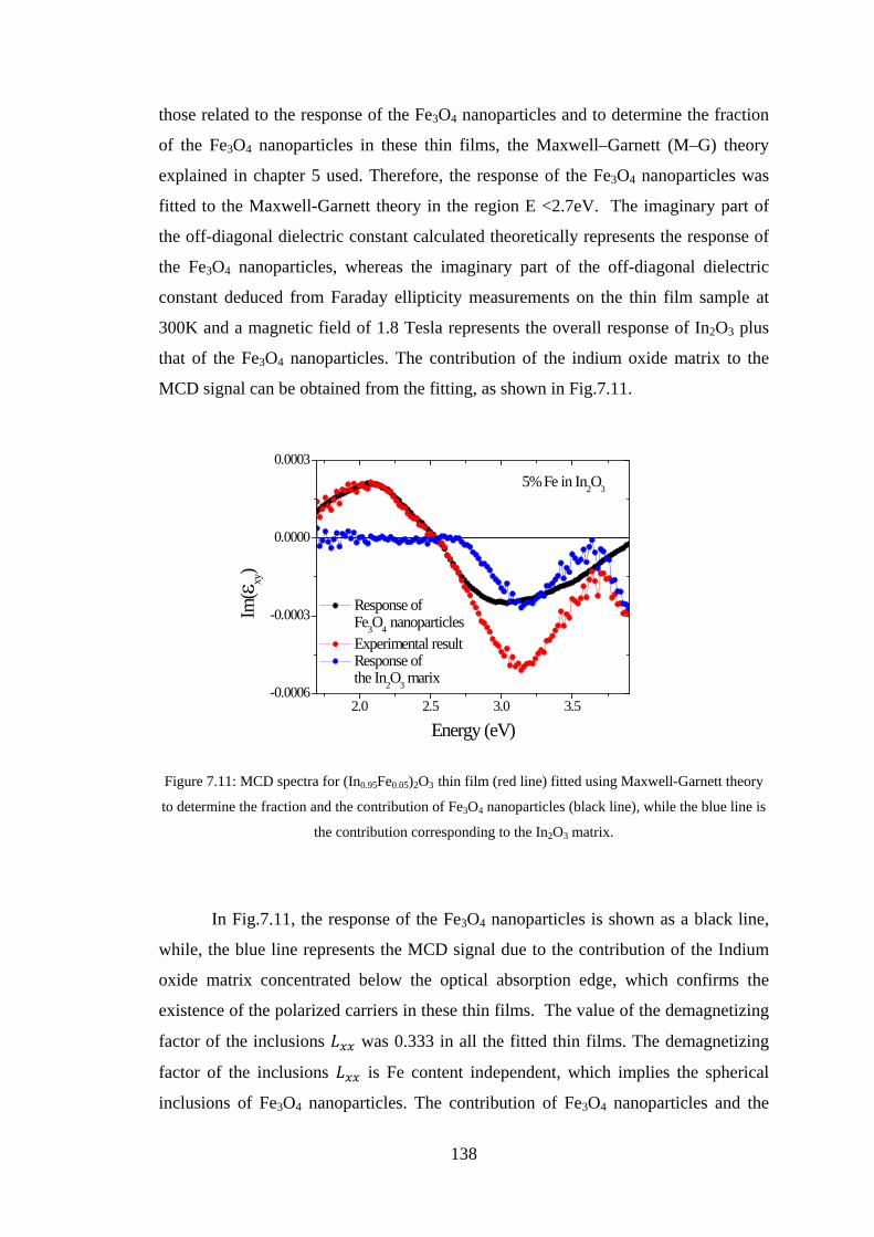
138
those related to the response of the Fe3O4 nanoparticles and to determine the fraction
of the Fe3O4 nanoparticles in these thin films, the Maxwell–Garnett (M–G) theory
explained in chapter 5 used. Therefore, the response of the Fe3O4 nanoparticles was
fitted to the Maxwell-Garnett theory in the region E <2.7eV. The imaginary part of
the off-diagonal dielectric constant calculated theoretically represents the response of
the Fe3O4 nanoparticles, whereas the imaginary part of the off-diagonal dielectric
constant deduced from Faraday ellipticity measurements on the thin film sample at
300K and a magnetic field of 1.8 Tesla represents the overall response of In2O3 plus
that of the Fe3O4 nanoparticles. The contribution of the indium oxide matrix to the
MCD signal can be obtained from the fitting, as shown in Fig.7.11.
2.0 2.5 3.0 3.5-0.0006
-0.0003
0.0000
0.00035% Fe in In2O3
Im(ε xy
)
Energy (eV)
Response of Fe3O4 nanoparticles
Experimental result Response of
the In2O3 marix
Figure 7.11: MCD spectra for (In0.95Fe0.05)2O3 thin film (red line) fitted using Maxwell-Garnett theory
to determine the fraction and the contribution of Fe3O4 nanoparticles (black line), while the blue line is
the contribution corresponding to the In2O3 matrix.
In Fig.7.11, the response of the Fe3O4 nanoparticles is shown as a black line,
while, the blue line represents the MCD signal due to the contribution of the Indium
oxide matrix concentrated below the optical absorption edge, which confirms the
existence of the polarized carriers in these thin films. The value of the demagnetizing
factor of the inclusions 𝐿𝑥𝑥 was 0.333 in all the fitted thin films. The demagnetizing
factor of the inclusions 𝐿𝑥𝑥 is Fe content independent, which implies the spherical
inclusions of Fe3O4 nanoparticles. The contribution of Fe3O4 nanoparticles and the
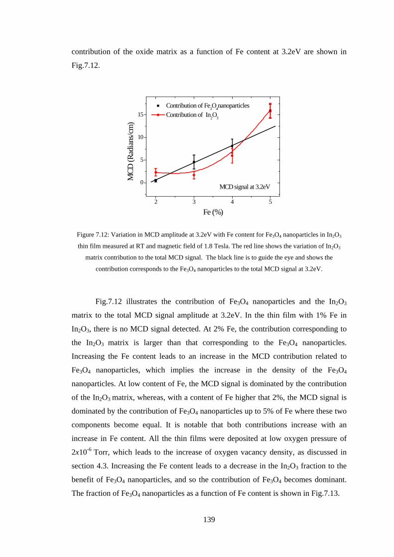
139
contribution of the oxide matrix as a function of Fe content at 3.2eV are shown in
Fig.7.12.
Contribution of Fe3O4nanoparticles Contribution of In2O3
2 3 4 5
0
5
10
15
MCD
(Rad
ians
/cm
)
Fe (%)
MCD signal at 3.2eV
Figure 7.12: Variation in MCD amplitude at 3.2eV with Fe content for Fe3O4 nanoparticles in In2O3
thin film measured at RT and magnetic field of 1.8 Tesla. The red line shows the variation of In2O3
matrix contribution to the total MCD signal. The black line is to guide the eye and shows the
contribution corresponds to the Fe3O4 nanoparticles to the total MCD signal at 3.2eV.
Fig.7.12 illustrates the contribution of Fe3O4 nanoparticles and the In2O3
matrix to the total MCD signal amplitude at 3.2eV. In the thin film with 1% Fe in
In2O3, there is no MCD signal detected. At 2% Fe, the contribution corresponding to
the In2O3 matrix is larger than that corresponding to the Fe3O4 nanoparticles.
Increasing the Fe content leads to an increase in the MCD contribution related to
Fe3O4 nanoparticles, which implies the increase in the density of the Fe3O4
nanoparticles. At low content of Fe, the MCD signal is dominated by the contribution
of the In2O3 matrix, whereas, with a content of Fe higher that 2%, the MCD signal is
dominated by the contribution of Fe3O4 nanoparticles up to 5% of Fe where these two
components become equal. It is notable that both contributions increase with an
increase in Fe content. All the thin films were deposited at low oxygen pressure of
2x10⁻⁶ Torr, which leads to the increase of oxygen vacancy density, as discussed in
section 4.3. Increasing the Fe content leads to a decrease in the In2O3 fraction to the
benefit of Fe3O4 nanoparticles, and so the contribution of Fe3O4 becomes dominant.
The fraction of Fe3O4 nanoparticles as a function of Fe content is shown in Fig.7.13.
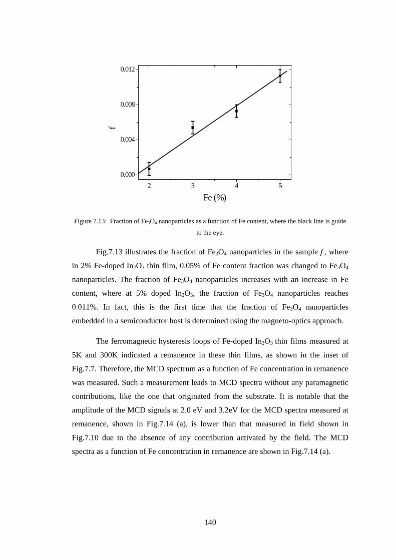
140
2 3 4 50.000
0.004
0.008
0.012
f
Fe (%)
Figure 7.13: Fraction of Fe3O4 nanoparticles as a function of Fe content, where the black line is guide
to the eye.
Fig.7.13 illustrates the fraction of Fe3O4 nanoparticles in the sample 𝑓, where
in 2% Fe-doped In2O3 thin film, 0.05% of Fe content fraction was changed to Fe3O4
nanoparticles. The fraction of Fe3O4 nanoparticles increases with an increase in Fe
content, where at 5% doped In2O3, the fraction of Fe3O4 nanoparticles reaches
0.011%. In fact, this is the first time that the fraction of Fe3O4 nanoparticles
embedded in a semiconductor host is determined using the magneto-optics approach.
The ferromagnetic hysteresis loops of Fe-doped In2O3 thin films measured at
5K and 300K indicated a remanence in these thin films, as shown in the inset of
Fig.7.7. Therefore, the MCD spectrum as a function of Fe concentration in remanence
was measured. Such a measurement leads to MCD spectra without any paramagnetic
contributions, like the one that originated from the substrate. It is notable that the
amplitude of the MCD signals at 2.0 eV and 3.2eV for the MCD spectra measured at
remanence, shown in Fig.7.14 (a), is lower than that measured in field shown in
Fig.7.10 due to the absence of any contribution activated by the field. The MCD
spectra as a function of Fe concentration in remanence are shown in Fig.7.14 (a).
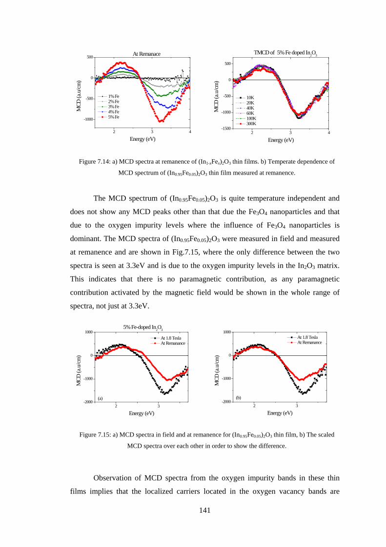
141
2 3 4
-1000
-500
0
500
MCD
(a.u
/cm)
Energy (eV)
1% Fe 2% Fe 3% Fe 4% Fe 5% Fe
At Remanace
2 3 4-1500
-1000
-500
0
500
MCD
(a.u
/cm)
Energy (eV)
10K 20K 40K 60K 100K 300K
TMCD of 5% Fe doped In2O3
Figure 7.14: a) MCD spectra at remanence of (In1-xFex)2O3 thin films. b) Temperate dependence of
MCD spectrum of (In0.95Fe0.05)2O3 thin film measured at remanence.
The MCD spectrum of (In0.95Fe0.05)2O3 is quite temperature independent and
does not show any MCD peaks other than that due the Fe3O4 nanoparticles and that
due to the oxygen impurity levels where the influence of Fe3O4 nanoparticles is
dominant. The MCD spectra of (In0.95Fe0.05)2O3 were measured in field and measured
at remanence and are shown in Fig.7.15, where the only difference between the two
spectra is seen at 3.3eV and is due to the oxygen impurity levels in the In2O3 matrix.
This indicates that there is no paramagnetic contribution, as any paramagnetic
contribution activated by the magnetic field would be shown in the whole range of
spectra, not just at 3.3eV.
At 1.8 Tesla At Remanance
2 3-2000
-1000
0
1000
MCD
(a.u
/cm
)
Energy (eV)
5% Fe-doped In2O3
(a)
MCD
(a.u
/cm)
2 3-2000
-1000
0
1000
Energy (eV)
At 1.8 Tesla At Remanance
(b)
Figure 7.15: a) MCD spectra in field and at remanence for (In0.95Fe0.05)2O3 thin film, b) The scaled
MCD spectra over each other in order to show the difference.
Observation of MCD spectra from the oxygen impurity bands in these thin
films implies that the localized carriers located in the oxygen vacancy bands are
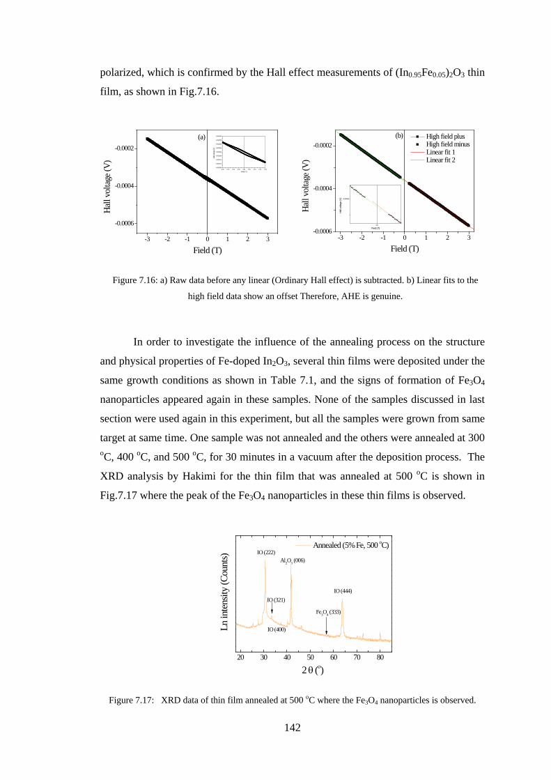
142
polarized, which is confirmed by the Hall effect measurements of (In0.95Fe0.05)2O3 thin
film, as shown in Fig.7.16.
-3 -2 -1 0 1 2 3
-0.0006
-0.0004
-0.0002
-0.20 -0.15 -0.10 -0.05 0.00 0.05 0.10 0.15 0.20-0.000380
-0.000375
-0.000370
-0.000365
-0.000360
-0.000355
-0.000350
-0.000345
-0.000340
Hall v
olta
ge (V
)
Field (T)
Hall
volta
ge (V
)
Field (T)
(a)
-3 -2 -1 0 1 2 3-0.0006
-0.0004
-0.0002
0.0
-0.00035
Hall v
olta
ge (V
)
Field (T)
Hall
volta
ge (V
)
Field (T)
High field plus High field minus Linear fit 1 Linear fit 2
(b)
Figure 7.16: a) Raw data before any linear (Ordinary Hall effect) is subtracted. b) Linear fits to the
high field data show an offset Therefore, AHE is genuine.
In order to investigate the influence of the annealing process on the structure
and physical properties of Fe-doped In2O3, several thin films were deposited under the
same growth conditions as shown in Table 7.1, and the signs of formation of Fe3O4
nanoparticles appeared again in these samples. None of the samples discussed in last
section were used again in this experiment, but all the samples were grown from same
target at same time. One sample was not annealed and the others were annealed at 300 oC, 400 oC, and 500 oC, for 30 minutes in a vacuum after the deposition process. The
XRD analysis by Hakimi for the thin film that was annealed at 500 oC is shown in
Fig.7.17 where the peak of the Fe3O4 nanoparticles in these thin films is observed.
20 30 40 50 60 70 80
Fe3O4 (333)
IO (400)
Al2O3 (006)
IO (444)IO (321)
Annealed (5% Fe, 500 oC)
Ln in
tens
ity (C
ount
s)
2 θ (ο)
IO (222)
Figure 7.17: XRD data of thin film annealed at 500 oC where the Fe3O4 nanoparticles is observed.
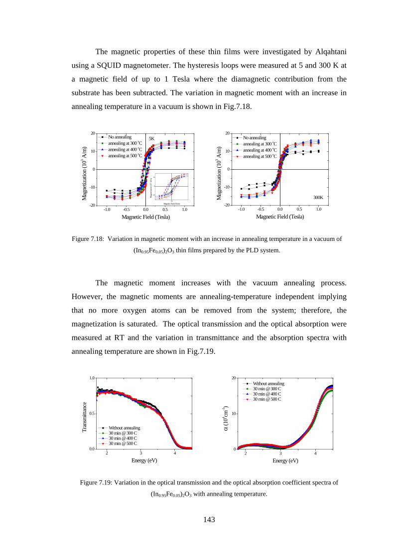
143
The magnetic properties of these thin films were investigated by Alqahtani
using a SQUID magnetometer. The hysteresis loops were measured at 5 and 300 K at
a magnetic field of up to 1 Tesla where the diamagnetic contribution from the
substrate has been subtracted. The variation in magnetic moment with an increase in
annealing temperature in a vacuum is shown in Fig.7.18.
-1.0 -0.5 0.0 0.5 1.0-20
-10
0
10
20
0.0
-10
0
10
Mag
netiz
atio
n (1
03 A/m
)
Magnetic Field (Tesla)
Mag
netiz
ation
(103 A
/m)
Magnetic Field (Tesla)
No annealing annealing at 300 oC annealing at 400 oC annealing at 500 oC
5K
-1.0 -0.5 0.0 0.5 1.0-20
-10
0
10
20
Mag
netiz
ation
(103 A
/m)
Magnetic Field (Tesla)
No annealing annealing at 300 oC annealing at 400 oC annealing at 500 oC
300K
Figure 7.18: Variation in magnetic moment with an increase in annealing temperature in a vacuum of
(In0.95Fe0.05)2O3 thin films prepared by the PLD system.
The magnetic moment increases with the vacuum annealing process.
However, the magnetic moments are annealing-temperature independent implying
that no more oxygen atoms can be removed from the system; therefore, the
magnetization is saturated. The optical transmission and the optical absorption were
measured at RT and the variation in transmittance and the absorption spectra with
annealing temperature are shown in Fig.7.19.
2 3 40.0
0.5
1.0
Tran
smitt
ance
Energy (eV)
Without annealing 30 min @ 300 C 30 min @ 400 C 30 min @ 500 C
2 3 40
10
20
α (1
04 cm-1)
Energy (eV)
Without annealing 30 min @ 300 C 30 min @ 400 C 30 min @ 500 C
Figure 7.19: Variation in the optical transmission and the optical absorption coefficient spectra of
(In0.95Fe0.05)2O3 with annealing temperature.
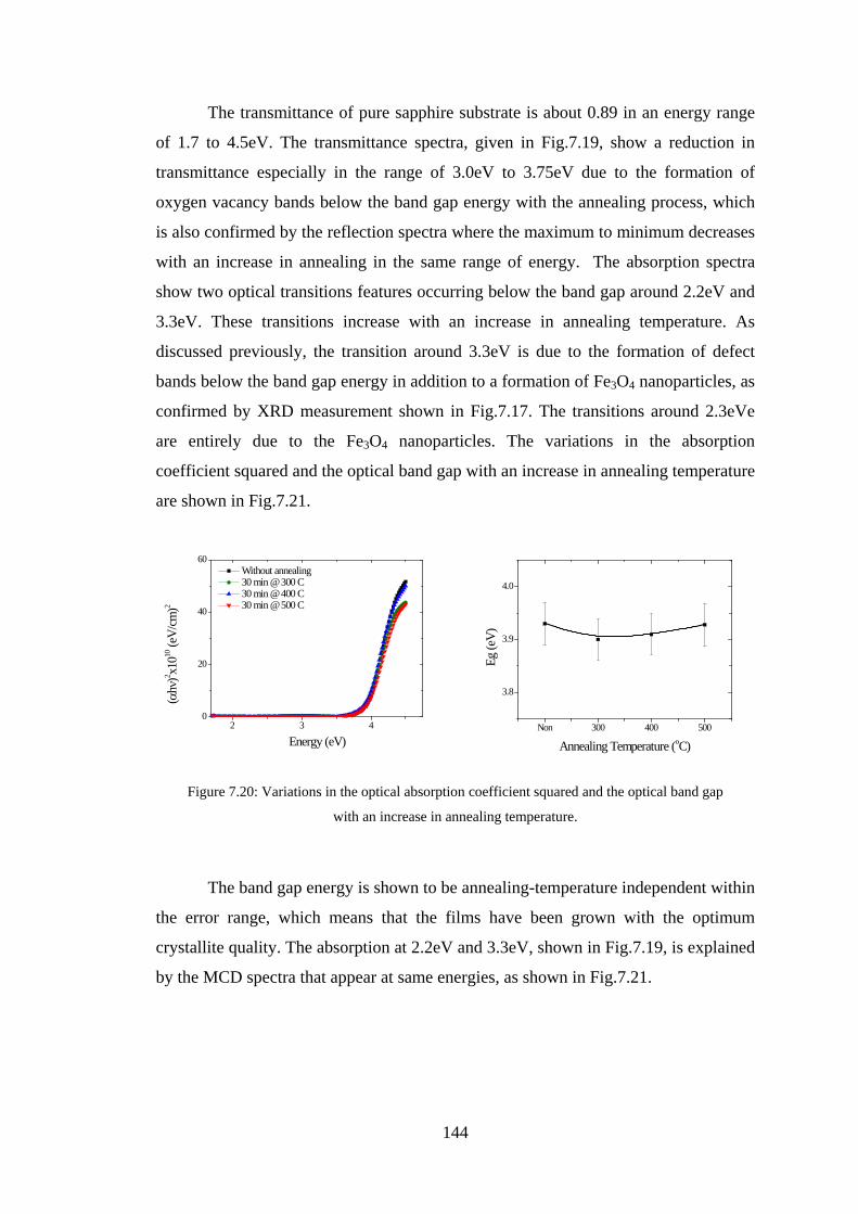
144
The transmittance of pure sapphire substrate is about 0.89 in an energy range
of 1.7 to 4.5eV. The transmittance spectra, given in Fig.7.19, show a reduction in
transmittance especially in the range of 3.0eV to 3.75eV due to the formation of
oxygen vacancy bands below the band gap energy with the annealing process, which
is also confirmed by the reflection spectra where the maximum to minimum decreases
with an increase in annealing in the same range of energy. The absorption spectra
show two optical transitions features occurring below the band gap around 2.2eV and
3.3eV. These transitions increase with an increase in annealing temperature. As
discussed previously, the transition around 3.3eV is due to the formation of defect
bands below the band gap energy in addition to a formation of Fe3O4 nanoparticles, as
confirmed by XRD measurement shown in Fig.7.17. The transitions around 2.3eVe
are entirely due to the Fe3O4 nanoparticles. The variations in the absorption
coefficient squared and the optical band gap with an increase in annealing temperature
are shown in Fig.7.21.
2 3 40
20
40
60
(αhν
)2 x10¹⁰
(eV/
cm)2
Energy (eV)
Without annealing 30 min @ 300 C 30 min @ 400 C 30 min @ 500 C
Non 300 400 500
3.8
3.9
4.0
Eg (e
V)
Annealing Temperature (oC)
Figure 7.20: Variations in the optical absorption coefficient squared and the optical band gap
with an increase in annealing temperature.
The band gap energy is shown to be annealing-temperature independent within
the error range, which means that the films have been grown with the optimum
crystallite quality. The absorption at 2.2eV and 3.3eV, shown in Fig.7.19, is explained
by the MCD spectra that appear at same energies, as shown in Fig.7.21.
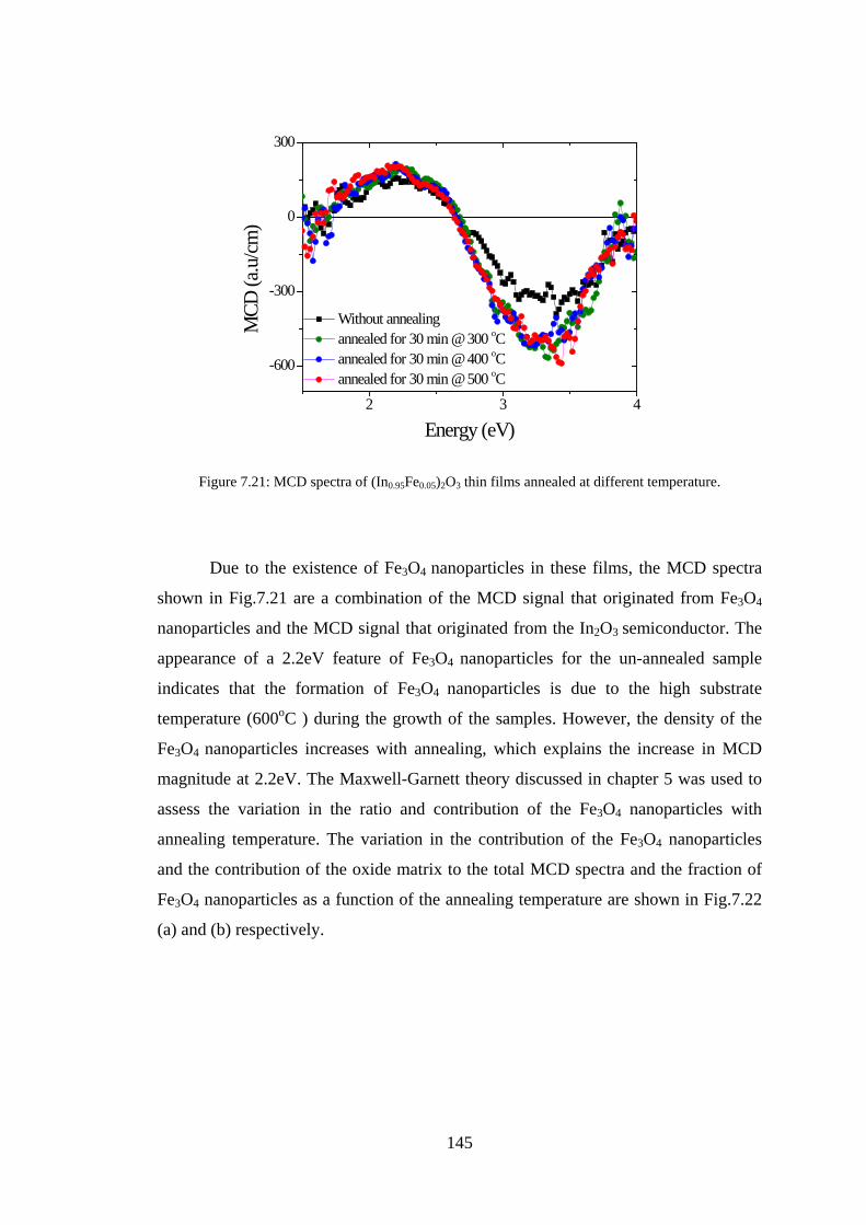
145
2 3 4
-600
-300
0
300
MCD
(a.u
/cm)
Energy (eV)
Without annealing annealed for 30 min @ 300 oC annealed for 30 min @ 400 oC annealed for 30 min @ 500 oC
Figure 7.21: MCD spectra of (In0.95Fe0.05)2O3 thin films annealed at different temperature.
Due to the existence of Fe3O4 nanoparticles in these films, the MCD spectra
shown in Fig.7.21 are a combination of the MCD signal that originated from Fe3O4
nanoparticles and the MCD signal that originated from the In2O3 semiconductor. The
appearance of a 2.2eV feature of Fe3O4 nanoparticles for the un-annealed sample
indicates that the formation of Fe3O4 nanoparticles is due to the high substrate
temperature (600oC ) during the growth of the samples. However, the density of the
Fe3O4 nanoparticles increases with annealing, which explains the increase in MCD
magnitude at 2.2eV. The Maxwell-Garnett theory discussed in chapter 5 was used to
assess the variation in the ratio and contribution of the Fe3O4 nanoparticles with
annealing temperature. The variation in the contribution of the Fe3O4 nanoparticles
and the contribution of the oxide matrix to the total MCD spectra and the fraction of
Fe3O4 nanoparticles as a function of the annealing temperature are shown in Fig.7.22
(a) and (b) respectively.

146
0 100 200 300 400 500
2
4
6
MCD
(Rad
ians/c
m)
Annealing Temperature (oC)
Contribution of Fe3O4 nanoparticles Contribution of oxide matrix
3.3 eV (a)
0 100 200 300 400 5000.003
0.004
0.005
f
Annealing Temperature (oC)
(b)
Figure 7.22: a) Variation in MCD amplitude at 3.3eV with annealing temperature. b) Variation in the
fraction of Fe3O4 nanoparticles with annealing temperature, where the data point at 0K represents the
the un-annealed sample and the black line is a guide for the eye.
Fig.7.22 (a) illustrates the MCD signal’s amplitude at 3.3eV, where the MCD
spectrum increases with an increase in annealing temperature. The contribution of the
Fe3O4 nanoparticles to the total MCD signal is larger than that of the oxide matrix.
The MCD signal related to the Fe3O4 nanoparticles is saturated with an increase in
annealing temperature, which is in agreement with the variation in the fraction of
Fe3O4 nanoparticles with an increase annealing temperature shown in Fig.7.22 (b).
The vacuum annealing process leads to some enhancement in MCD signal of the
oxide matrix supported by the increases in the oxygen vacancy density. The fraction
of Fe3O4 nanoparticles increases with an increase in annealing temperature. The
fraction of Fe3O4 nanoparticles seems to be saturated at 0.5%.
In order to explore the effect of tin doping on the optical and magneto-optical
properties of Fe-doped In2O3, three iron doped indium oxide (In0.95Fe0.05)2O3 thin
films doped with 0, 5 and 10% of tin were deposited using the PLD system as shown
in Table 7.1. The magnetic properties of these thin films were not measured. The
variation of the optical transmission spectra and the optical band gap energy with tin
content are shown in Fig.7.23 and Fig.7.24 respectively.
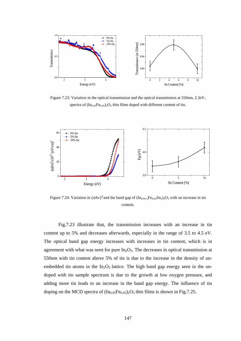
147
2 3 40.0
0.5
1.0
Tran
smitt
ance
Energy (eV)
0% Sn 5% Sn 10% Sn
0 2 4 6 8 10
0.80
0.84
0.88
Tran
smitt
ance
(at 5
50nm
)
Sn Content (%)
Figure 7.23: Variation in the optical transmission and the optical transmission at 550nm, 2.3eV,
spectra of (In0.95Fe0.05)2O3 thin films doped with different content of tin.
2 3 40
20
40
60
(αhν
)2 x10¹⁰
(eV/
cm)2
Energy (eV)
0% Sn 5% Sn 10% Sn
0 5 103.9
4.0
4.1
Eg (e
V)
Sn Content (%)
Figure 7.24: Variation in (𝛼ℎ𝜈)2and the band gap of (In0.95-yFe0.05Sny)2O3 with an increase in tin
content.
Fig.7.23 illustrate that, the transmission increases with an increase in tin
content up to 5% and decreases afterwards, especially in the range of 3.5 to 4.5 eV.
The optical band gap energy increases with increases in tin content, which is in
agreement with what was seen for pure In2O3. The decreases in optical transmission at
550nm with tin content above 5% of tin is due to the increase in the density of un-
embedded tin atoms in the In2O3 lattice. The high band gap energy seen in the un-
doped with tin sample spectrum is due to the growth at low oxygen pressure, and
adding more tin leads to an increase in the band gap energy. The influence of tin
doping on the MCD spectra of (In0.95Fe0.05)2O3 thin films is shown in Fig.7.25.

148
2 3 4-2000
-1000
0
1000
2000
MCD
(a.u
/cm)
Energy (eV)
5% Fe 5% Fe + 5% Sn 5% Fe + 10% Sn
Figure 7.25: Variation in MCD spectrum of (In0.95Fe0.05)2O3 thin films with tin content.
As found previously, the MCD feature seen at 2.2eV for un-doped thin film is
related to Fe3O4 nanoparticles. It is surprising that for the thin films doped with tin,
the 2.2eV feature totally disappears, which implies that adding tin may help the Fe
atoms to embed within the In2O3 lattice and prevent the formation of nanoparticles.
This result supports our previous observation, specifically, that metallic Co disappears
also for thin films doped with tin, as discussed in chapter 6. The feature at 3.4eV for
the un-doped with tin sample is a combination of the MCD coming from the Fe3O4
nanoparticles and the MCD coming from the states of oxygen vacancies produced by
the growth at low oxygen pressure. For tin doped samples, the MCD feature at 3.4eV
increased when tin was added to the oxide matrix and the optical absorption edge
shifted to higher energy as expected and as was stated previously for pure and Co-
doped In2O3. The contribution of tin atoms to the MCD spectrum is increasing the
carrier concentration and, most probably, fighting the formation of cluster and
nanoparticles to the benefit of the oxygen vacancy bands which are formed below the
optical absorption edge.
In order to explore the variation in the optical and magneto-optical properties
of Fe-doped In2O3 with oxygen partial pressure, two (In0.95Fe0.05)2O3 thin films were
deposited on sapphire (Al2O3) substrates using pulsed laser ablation. The samples
were prepared by Xiao-Hong Xu’s group from Shanxi Normal University, China; this
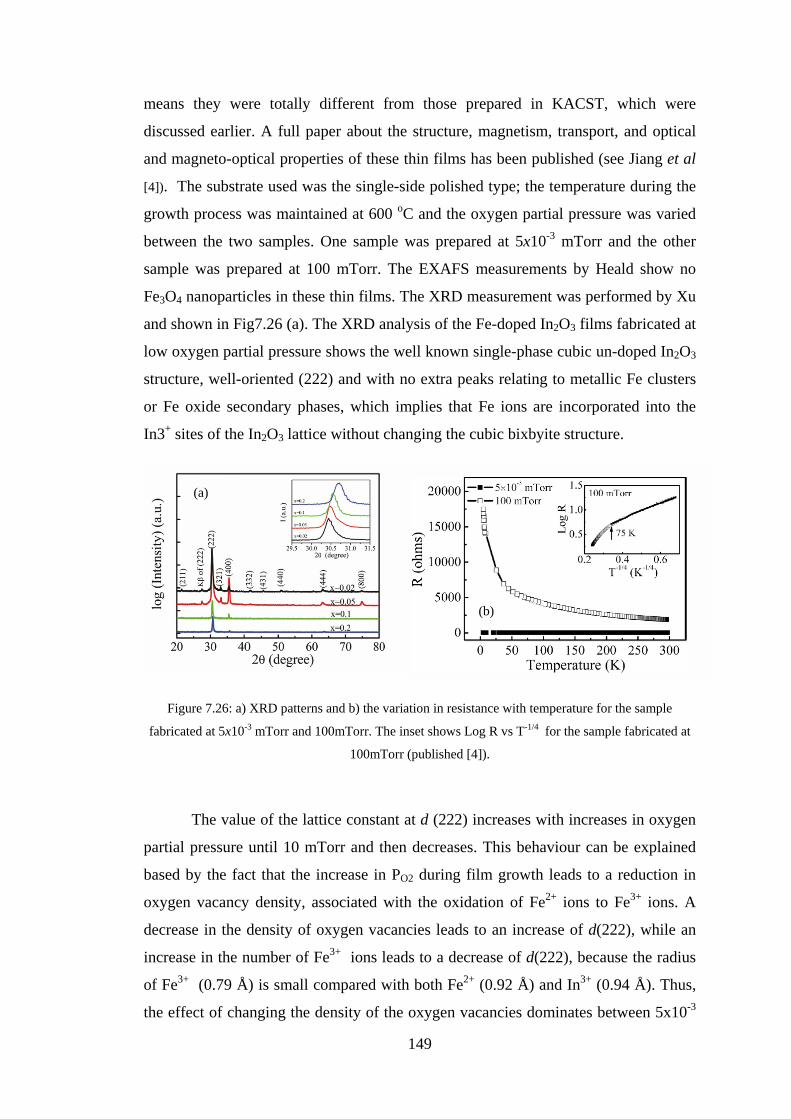
149
means they were totally different from those prepared in KACST, which were
discussed earlier. A full paper about the structure, magnetism, transport, and optical
and magneto-optical properties of these thin films has been published (see Jiang et al
[4]). The substrate used was the single-side polished type; the temperature during the
growth process was maintained at 600 oC and the oxygen partial pressure was varied
between the two samples. One sample was prepared at 5x10⁻³ mTorr and the other
sample was prepared at 100 mTorr. The EXAFS measurements by Heald show no
Fe3O4 nanoparticles in these thin films. The XRD measurement was performed by Xu
and shown in Fig7.26 (a). The XRD analysis of the Fe-doped In2O3 films fabricated at
low oxygen partial pressure shows the well known single-phase cubic un-doped In2O3
structure, well-oriented (222) and with no extra peaks relating to metallic Fe clusters
or Fe oxide secondary phases, which implies that Fe ions are incorporated into the
In3+ sites of the In2O3 lattice without changing the cubic bixbyite structure.
Figure 7.26: a) XRD patterns and b) the variation in resistance with temperature for the sample
fabricated at 5x10⁻³ mTorr and 100mTorr. The inset shows Log R vs T-1/4 for the sample fabricated at
100mTorr (published [4]).
The value of the lattice constant at d (222) increases with increases in oxygen
partial pressure until 10 mTorr and then decreases. This behaviour can be explained
based by the fact that the increase in PO2 during film growth leads to a reduction in
oxygen vacancy density, associated with the oxidation of Fe2+ ions to Fe3+ ions. A
decrease in the density of oxygen vacancies leads to an increase of d(222), while an
increase in the number of Fe3+ ions leads to a decrease of d(222), because the radius
of Fe3+ (0.79 Å) is small compared with both Fe2+ (0.92 Å) and In3+ (0.94 Å). Thus,
the effect of changing the density of the oxygen vacancies dominates between 5x10⁻³
(a)
(b)

150
mTorr and 10 mTorr, while the effect of changing the ionization state of Fe dominates
for pressures between 10 and 100 mTorr, as confirmed by the XPS analysis [5]. The
variation of resistance with temperature of the sample grown at 100 mTorr shows a
metallic behaviour, whereas the sample grown at 5x10⁻³ mTorr shows classic
semiconductor behaviour, as shown in Fig.7.26 (b).
The transport properties using the Van der Pauw four-point configuration and
the Hall effect measurements were investigated by Xu. The carrier concentration (nc)
measured at RT is 2.40x1018 cm-3 and 4.27x1020 cm-3 for the thin films deposited at
100 mTorr and 5x10⁻³ mTorr respectively. The resistivity (ρ) is 2.06x10⁻¹ Ω.cm and
9.25x10⁻⁴ Ω.cm for the thin films deposited at 100 mTorr and 5x10⁻³ mTorr
respectively. Therefore, the carrier concentration decreases while the resistivity
increases with an increase in oxygen partial pressure. The dependence of resistivity
and carrier density on oxygen partial pressure is due to the variation in the
concentration of oxygen vacancies and Fe2+ ions in these films. This variation is
because the thin film fabricated at high oxygen pressure of 100 mTorr lies in the
insulating regime, whereas the thin film fabricated at low oxygen pressure of 5x10⁻³
mTorr lies in the metallic regime.
The magnetic measurements were performed by my colleague Alqahtani using
a SQUID magnetometer. The hysteresis loops were measured at 5 and 300 K for both
samples; the hysteresis loops for the sample fabricated at 5x10⁻³ mTorr are shown in
Fig.27 (a) and those for the one fabricated at 100 mTorr are shown in Fig.27 (b). The
diamagnetic contribution from the substrate has been subtracted from the loops.
Figure 7.27: The hysteresis loops for the samples fabricated at (a) 5x10⁻³ mTorr and (b) 100mTorr.
(published [4] in Oe unit).

151
The samples exhibit a clear RT ferromagnetic behaviour. The magnetization
of the sample fabricated at 5x10⁻³ mTorr shows temperature independent behaviour,
which indicates that the Curie temperature Tc of the sample is above RT, which is
required for developing practical spintronic devices. In contrast, the magnetization of
the sample fabricated at 100 mTorr shows temperature dependent behaviour, which
mean that in addition to the ferromagnetic moment there is also a paramagnetic
contribution. The influence of oxygen partial pressure on the electronic structure is
revealed through the study of the optical properties of these films. Variation in the
optical absorption spectra with temperature for both samples was measured. The
temperature dependence of the absorption spectra of the sample fabricated at 5x10⁻³
mTorr is given in Fig.28 (a) and for the samples fabricated at 100 mTorr is given in
Fig.28 (b).
2.5 3.0 3.5 4.00
5
10
α2 (109 cm
-2)
Energy (eV)
10 K 50 K 300 K
(a)
2.5 3.0 3.5 4.00
5
10
α2 (1
09 cm-2)
Energy (eV)
10 K 50 K 300 K
(b)
Figure 7.28: Variation in the absorption coefficient squared with energy for the sample fabricated
at (a) 5x10⁻³ mTorr and (b) 100mTorr [4] (published in different format).
The absorption is temperature dependent in both samples due to the activation
of phonons at RT. However, the absorption is more temperature dependent for the
sample fabricated at 5x10⁻³ mTorr, which implies that at low temperatures, the
localized states present in the sample fabricated at 100 mTorr activate the transition
more effectively than do the delocalized impurity band states in the sample fabricated
at 5x10⁻³ mTorr. The optical band gap was calculated using the Tauc plot method and
the variation in optical band gap energy with oxygen partial pressure is shown in
Fig.7.29.

152
5x10⁻³ mTorr 100 mTorr
2.5 3.0 3.5 4.00
20
40
0 20 40 60 80 1003.80
3.85
3.90
Eg (e
V)
Oxygen Partial Pressure (mTorr)
(αhν
)2 x10¹⁰
(eV/
cm)2
Energy (eV)
Figure 7.29: Variation in the optical band gap energy of (In0.95Fe0.05)2O3 thin films with
oxygen partial pressure.
The optical band gap increases with a decrease in oxygen partial pressure,
which is consistent with a previous result for pure In2O3. Growth at low oxygen
partial pressure leads to an increase in carrier density; therefore, the optical band gap
energy increased. The MCD was measured with the applied magnetic field up to 1.8
Tesla in Faraday geometry as a function of temperature. The MCD spectra were
obtained after the subtraction of the MCD spectra of the substrate. The magneto-optic
spectrum measured shows an MCD signal from the film fabricated at 5x10⁻³ mTorr
only located below the band gap energy as shown in Fig.7.30.
2 3 4-3000
-1500
0
1500
MCD
(Deg
ree/c
m)
Energy (eV)
5x10⁻³ mTorr 100 mTorr
Figure 7.30: Variation in MCD spectra of 5% Fe-doped In2O3 with oxygen partial pressure
measured at RT and a magnetic field of 1.8 Tesla.
153
Fig.7.30 shows that the film fabricated at 100 mTorr exhibits no MCD signal
whereas the film fabricated at 5x10⁻³ mTorr displays a positive MCD signal originated
from the forbidden transitions states in the energy range 2.75 < E < 3.70 eV. The
MCD signal measured the difference in the density of states at the Fermi energy level.
Therefore, in the case of the film fabricated at 100 mTorr, the energy states near the
Fermi energy level are localized; thus, the energy density is potential dependent, but
not energy dependent. As a result, any spin splitting of these localized states does not
lead to unequal densities of states at the Fermi energy level. In contrast, the film
fabricated at 5x10⁻³ mTorr is metallic and contains a fraction of Fe2+ ions. Fe2+ ions
act as acceptors that will generate a spin-polarized conduction band. The density of
states in a conduction band is strongly energy dependent. As a result, the spin splitting
of these states leads to unequal densities of states at the Fermi energy level, which
results in the strong MCD spectrum.
7.3 Conclusion This chapter investigated the influence of Fe-doping content, oxygen partial
pressure, vacuum annealing process, and doping with tin on the optical and magneto-
optical properties of Fe-doped In2O3 thin films. XRD and EXAFS measurements
show that some thin films contain a fraction of Fe3O4 nanoparticles. Therefore, the
Maxwell-Garnett theory was used for the first time to measure the fraction of Fe3O4
nanoparticles and to distinguish between the MCD response of the host matrix and
that of Fe3O4 nanoparticles. The magneto-optical measurements method was found to
be more accurate and quantitative than the EXAFS measurements. The magneto-
optical measurements revealed that the fraction of Fe3O4 nanoparticles increases
linearly with an increase in Fe content and the density of the oxygen vacancy bands
increases with an increase in Fe content. The MCD is due to responses of the Fe3O4
nanoparticles which, in turn, are due the responses of In2O3 matrix; the density of
these polarized carriers increases with an increase in Fe content. Also, the fraction of
Fe3O4 nanoparticles increases with an increase in the annealing in a vacuum
temperature. This fraction can be reduced by doping with tin, as Sn-doping prevents
the formation of Fe3O4 nanoparticles and increases the density of carriers and the
oxygen vacancy bands. The vacuum annealing process leads to an increase in the
MCD response due to the Fe3O4 nanoparticles and that related to the In2O3 matrix.

154
However, the vacuum annealing process is not responsible for the formation of Fe3O4
nanoparticles, as the Fe3O4 nanoparticles have been observed in un-annealed samples.
Ferromagnetism at room temperature was observed in Fe-doped In2O3 thin
films that did not contain any Fe3O4 nanoparticles. The observed ferromagnetism is
due to the substitution of Fe for In and does not arise from the presence of either
metallic Fe clusters or Fe oxides secondary phases in the films. We found that the
ferromagnetism, carrier concentration, and the density of oxygen vacancies depend
sensitively on oxygen partial pressure during the growth, where the density of oxygen
vacancy increases with decreases in oxygen partial pressure.
155
7.4 References 1. E. Burstein, Phys. Rev. 93, 632 (1954).
2. W. F. J. Fontijn, P. J. V.D. Zaag, M. A. C. Devillers, V. A. M. Brabers and R.
Metselaar, Phys. Rev. B 56, 5432 (1997).
3. X. Zhang, J. Schoenes and P. Wachter, Solid State Commun. 39, 189-192
(1981).
4. F. X. Jiang, X. H. Xu, J. Zhang, X. C. Fan, H. S. Wu, M. Alshammari, Q.
Feng, H. J. Blythe, D. S. Score, K. Addison, M. Al-Qahtani and G. A.
Gehring, J. Appl. Phys. 109, 053907 (2011).
5. M. Descostes, F. Mercier, N. Thromat, C. Beaucaire and M. Gautier-Soyer,
Appl. Surf. Sci. 165, 288-302 (2000).

156
Chapter 8 Multiferroic GdMnO3
8.1 Introduction
The rare-earth elements, from lanthanum (La) to lutetium (Lu), are an example
of incomplete inner f shells, but their outer electrons are almost identical. The rare
earth elements exhibit a strong paramagnetism at room temperature and above and
have a large net magnetic moment. The total magnetic moment of these elements
originates from the electrons of unfilled 4f shells due to both orbital and spin motions.
The 4f shell is a deep shell and the outer electron shells work to shield against the
other ions in the field. Therefore, the orbital moments remain unquenched. At low
temperatures, the magnetic behaviour of the rare earth elements is complex. All the
rare earth elements show ferromagnetic or antiferromagnetic behaviour over a range
of temperatures. The RMnO3 rare-earth manganites are one of the well-known
multiferroic materials which exhibit ferromagnetic and ferroelectric properties at the
same time in the same phase. One of the rare-earth elements is gadolinium, which is
discussed in this chapter. This chapter begins with a review of the multiferroic
materials and focuses on GdMnO3; then, the optical and magneto-optical properties of
GdMnO3 are presented. The data presented in this chapter have been submitted for
publication.
8.2 Literature Review
Multiferroic materials have attracted considerable attention due to their
intriguing physical properties. These materials exhibit ferromagnetic and ferroelectric
properties simultaneously in the same phase. The idea is to control the magnetization
of multiferroic materials by an electric field and to control their electrical properties
by the induction of polarization by a magnetic field. This phenomenon provides
another route for linking magnetic and electric properties for a single material, which
is called the magnetoelectric effect or magnetoelectric coupling [1-4]. Thus, the
magnetoelectric effect can be used as a key parameter to develop novel
magnetoelectric and magneto-optical devices. These novel devices require suitable
materials in thin film forms, rather than in bulk forms but, until the present time, there
have not been enough studies on multiferroic thin films [5].
157
The magnetoelectric effect has a long history starting from its discovery by
Rontgen in 1888, when a moving dielectric became magnetized when placed in an
electric field. This discovery was followed by contributions from Curie, Debye and
others until today. A comprehensive history of magnetoelectrics can be found in a
topical review called Revival of the magnetoelectric effect by Manfred Fiebig [6].
Recently, an extraordinary renaissance of magnetoelectric effect publications has been
observed, as shown in Fig.8.1.
Figure 8.1: Publications per year with ‘magnetoelectric’ in the title [6].
The revival of multiferroics has been powered by many factors, such as the
fabrication of high-quality single crystalline samples [3, 7], the improvement of first-
principles computational techniques [8], and the developments in thin-film growth
techniques, which have allowed the properties of existing materials to be modified by
strain engineering [9]; this was unachievable by traditional methods.
In ferroic and multiferroic materials, the magnetic field H controls the
magnetization M, where the magnetization is spontaneously formed to produce
ferromagnetism. The electric field E controls the polarization P, where the
polarization is spontaneously formed to produce ferroelectricity. The stress σ controls
the strain ε, where the strain is spontaneously formed to produce ferroelasticity.
Therefore, in multiferroic materials, the coexistence of at least two ferroic forms of
ordering leads to additional interactions. Thus, in a magnetoelectric multiferroic, an
electric field E may control M or a magnetic field H may control P [10].

158
Figure 8.2: Phase control in ferroics and multiferroics[10].
The RMnO3 rare-earth manganites (where R= Pr, Nd, Sm, Eu, Gd, and Tb)
have attracted more attention than the other multiferroic materials, not only for their
magnetoelectric properties but also for their crystal structure. Depending on the rare-
earth ionic radius, the RMnO3 form either an orthorhombic phase or a hexagonal
phase. Orthorhombic RMnO3 has ferroelectric and magnetic properties below the
Néel temperature (TN ~ 41 K) [3, 11, 12], which is quite a low temperature, and
charge, spin, orbital, and lattice subsystems are linked very tightly. Thus, the strain in
the thin films of these materials plays an important role in the formation of their
properties. Therefore, the effects of the strain need to be clarified. On the other hand,
hexagonal RMnO3 or (hexa-RMnO3) has ferroelectric and magnetic properties up to
590 K [13], but the magnetoelectric coupling for hexa-RMnO3 is still smaller than that
of orthorhombic RMnO3 [1, 13, 14].
Figure 8.3: Phase diagram of GdMnO3 for magnetic fields applied along the b axis. Shaded areas signal
regions of strong hysteresis [15, 16].

159
The influence of magnetic field, pressure and temperature upon the
magnetization and the dielectric properties in bulk single crystals of GdMnO3 has
been investigated [15-18]. It has been found that a magnetic field is necessary to
induce multiferroicity in GdMnO3 , and H-T phases are field orientations along a, b,
and c axis dependent. In Fig. 3, the first transition occurs at 42K between the
paramagnetic (PM) phase and an incommensurate antiferromagnetic (ICAFM) phase.
At 20K and fields greater than 2T, the ICAFM transforms into a canted A-type
antiferromagnet (cAFM). At 12K, a transition to a ferroelectric (FE) phase occurs. On
the other hand, below ~20K and fields smaller than 2T there is strong hysteresis so
that several phases can coexist. These phases are very dependent on pressure due to
the existence of a ferroelectric phase. The phase boundaries depend on both the
magnitude and the direction of the magnetic field, which means the magnetic
structure of GdMnO3 needs to be determined unambiguously. Because the H-T phases
are field-orientation dependent, one might consider that, for thin films of the
manganites and using the epitaxial strain, the physical properties can be changed [19]
and the magnetic and electronic phases can be controlled [20]. The optical absorption
spectra of RMnO3 thin films at room temperature are shown in Fig.8.4.
Figure 8.4: Absorption spectra of RMnO3 thin films at room temperature shows intersite
transition peak at 2 eV [21].
The optical absorption spectra for RMnO3 manganites shown in Fig.8.4
illustrated a clear peak occurring near 2eV [21]; this has been confirmed for LaMnO3
and NdMnO3[22] . This absorption peak is caused by the charge transfer excitation
160
between Mn ions due to the different canting of the Mn d-orbitals and is dependent on
the directions of the Mn spins. Magneto-optical studies on TbMnO3 single crystal in a
magnetic field have also shown a strong feature occurring near 3eV[23]. This chapter
investigates the effect of strain caused by lattice mismatch to different substrates on
the magnetic and magneto-optical properties of GdMnO3.
8.3 Experiment Details, Results, and Discussion
Stoichiometric mixtures of Gd2O3 and MnO2 were used to prepare a target of
GdMnO3. Then, the target was used to grow GdMnO3 thin films on LaAlO3 and
SrTiO3 substrates using dc magnetron sputtering. The GdMnO3 thin films were
deposited in a mixture of Ar and O2 environments at a pressure of 1-2 mTorr. The
substrates’ temperature was sustained at 650°C with the [110]-direction parallel to the
plane of the substrate. The thickness of the thin films varied between 100-200 nm.
The structures of the thin films were characterized by x-ray diffraction, as shown in
Fig.8.5. The growth of the thin films and the XRD measurements were done by Ya.
Mukovskii from the National University of Science and Technology, Moscow,
Russia.
Figure 8.5: X-ray data of GdMnO3 films on the SrTiO3 and LaAlO3 substrates.
The XRD diffraction pattern in Fig.8.5 shows epitaxial growth, and some
peaks appear at values 22o and 47
o arising from GdMnO3 planes. The relatively
stronger peak intensity at is indicative of the preferential (431) orientation
of GdMnO3 thin films. In fact, the LaAlO3 substrate was found to be heavily twinned,
and the SrTiO3 substrate undergoes a structural transition at ~100K; this may produce
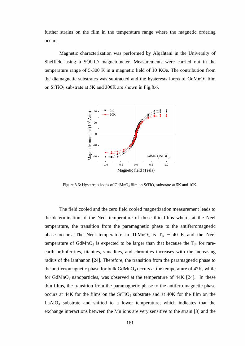
161
further strains on the film in the temperature range where the magnetic ordering
occurs.
Magnetic characterization was performed by Alqahtani in the University of
Sheffield using a SQUID magnetometer. Measurements were carried out in the
temperature range of 5-300 K in a magnetic field of 10 KOe. The contribution from
the diamagnetic substrates was subtracted and the hysteresis loops of GdMnO3 film
on SrTiO3 substrate at 5K and 300K are shown in Fig.8.6.
-1.0 -0.5 0.0 0.5 1.0
-40
-20
0
20
40
GdMnO3/SrTiO
3
Mag
net
ic m
om
ent
(10
3 A
/m)
Magnetic field (Tesla)
5K
10K
Figure 8.6: Hysteresis loops of GdMnO3 film on SrTiO3 substrate at 5K and 10K.
The field cooled and the zero field cooled magnetization measurement leads to
the determination of the Néel temperature of these thin films where, at the Néel
temperature, the transition from the paramagnetic phase to the antiferromagnetic
phase occurs. The Néel temperature in TbMnO3 is TN ~ 40 K and the Néel
temperature of GdMnO3 is expected to be larger than that because the TN for rare-
earth orthoferrites, titanites, vanadites, and chromites increases with the increasing
radius of the lanthanon [24]. Therefore, the transition from the paramagnetic phase to
the antiferromagnetic phase for bulk GdMnO3 occurs at the temperature of 47K, while
for GdMnO3 nanoparticles, was observed at the temperature of 44K [24]. In these
thin films, the transition from the paramagnetic phase to the antiferromagnetic phase
occurs at 44K for the films on the SrTiO3 substrate and at 40K for the film on the
LaAlO3 substrate and shifted to a lower temperature, which indicates that the
exchange interactions between the Mn ions are very sensitive to the strain [3] and the
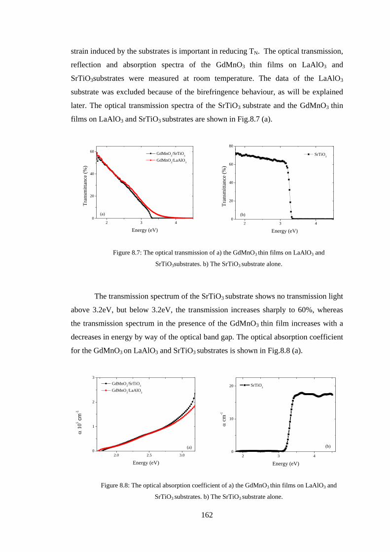
162
strain induced by the substrates is important in reducing TN. The optical transmission,
reflection and absorption spectra of the GdMnO3 thin films on LaAlO3 and
SrTiO3substrates were measured at room temperature. The data of the LaAlO3
substrate was excluded because of the birefringence behaviour, as will be explained
later. The optical transmission spectra of the SrTiO3 substrate and the GdMnO3 thin
films on LaAlO3 and SrTiO3 substrates are shown in Fig.8.7 (a).
2 3 40
20
40
60
Tra
nsm
itta
nce
(%
)
Energy (eV)
GdMnO3/SrTiO
3
GdMnO3/LaAlO
3
(a)
2 3 40
20
40
60
80
Tra
nsm
itta
nce
(%
)
Energy (eV)
SrTiO3
(b)
Figure 8.7: The optical transmission of a) the GdMnO3 thin films on LaAlO3 and
SrTiO3substrates. b) The SrTiO3 substrate alone.
The transmission spectrum of the SrTiO3 substrate shows no transmission light
above 3.2eV, but below 3.2eV, the transmission increases sharply to 60%, whereas
the transmission spectrum in the presence of the GdMnO3 thin film increases with a
decreases in energy by way of the optical band gap. The optical absorption coefficient
for the GdMnO3 on LaAlO3 and SrTiO3 substrates is shown in Fig.8.8 (a).
2.0 2.5 3.00
1
2
3
GdMnO3/SrTiO
3
GdMnO3/LaAlO
3
1
05 c
m-1
Energy (eV)
(a)
2 3 40
10
20
c
m-1
Energy (eV)
SrTiO3
(b)
Figure 8.8: The optical absorption coefficient of a) the GdMnO3 thin films on LaAlO3 and
SrTiO3 substrates. b) The SrTiO3 substrate alone.

163
Fig.8.8 (a) confirms the formation of a shoulder of absorption below the
optical band gap energy 3.25eV; this shoulder of absorption does not exist in the
absorption spectrum of SrTiO3 substrate shown in (b). Above the optical band gap
energy, the absorption is dominated by the substrate absorption edge [25]. The
absorption of GdMnO3 on the LaAlO3 substrate shows a longer shoulder of absorption
up to the optical band gap ~3.48eV and then rises beyond. With the existence of the
GdMnO3 thin film, the absorption between the band gap energy and higher energies is
due to charge transfer transitions from the oxygen 2p band to the unoccupied Mn d
states.
2 30
2
4
6
2 (
10
10 c
m-2)
Energy (eV)
GdMnO3/SrTiO
3
GdMnO3/LaAlO
3
(a)
2 3 40
200
400
2 c
m-2
Energy (eV)
SrTiO3
(b)
Figure 8.9: The absorption squared for a) the GdMnO3 thin films on LaAlO3 and
SrTiO3substrates taken at room temperature. b) The SrTiO3 substrate.
The MCD spectra at room temperature for both films are shown in Fig.8.10.
2 3
-0.03
0.00
0.03
0.06
Energy (eV)
MC
D (
a.u
)
-3
-2
-1
0
Ro
tati
on
(a.
u)
(a) GdMnO3/SrTiO
3
2 3-0.03
0.00
0.03
Energy (eV)
MC
D (
a.u)
-0.03
0.00
0.03
Rota
tion (
a.u)
(b) GdMnO3/LaAlO
3
Figure 8.10: MCD and rotation spectra for (a) GaMnO3 on SrTiO3 (b) GaMnO3 on LaAlO3
where the substrate contribution is included. The measurement was taken at room temperature
and a magnetic field of 1.8Tesla.
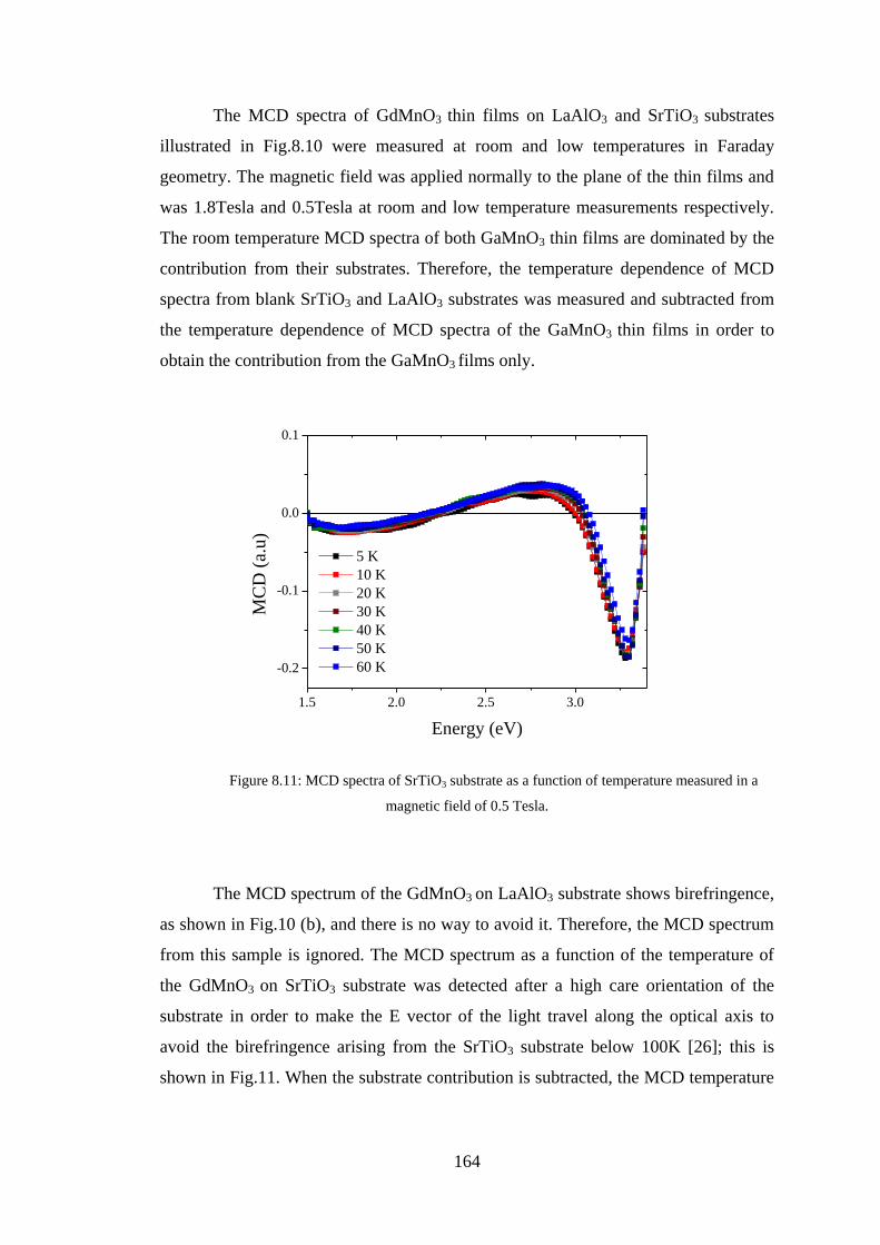
164
The MCD spectra of GdMnO3 thin films on LaAlO3 and SrTiO3 substrates
illustrated in Fig.8.10 were measured at room and low temperatures in Faraday
geometry. The magnetic field was applied normally to the plane of the thin films and
was 1.8Tesla and 0.5Tesla at room and low temperature measurements respectively.
The room temperature MCD spectra of both GaMnO3 thin films are dominated by the
contribution from their substrates. Therefore, the temperature dependence of MCD
spectra from blank SrTiO3 and LaAlO3 substrates was measured and subtracted from
the temperature dependence of MCD spectra of the GaMnO3 thin films in order to
obtain the contribution from the GaMnO3 films only.
1.5 2.0 2.5 3.0
-0.2
-0.1
0.0
0.1
MC
D (
a.u
)
Energy (eV)
5 K
10 K
20 K
30 K
40 K
50 K
60 K
Figure 8.11: MCD spectra of SrTiO3 substrate as a function of temperature measured in a
magnetic field of 0.5 Tesla.
The MCD spectrum of the GdMnO3 on LaAlO3 substrate shows birefringence,
as shown in Fig.10 (b), and there is no way to avoid it. Therefore, the MCD spectrum
from this sample is ignored. The MCD spectrum as a function of the temperature of
the GdMnO3 on SrTiO3 substrate was detected after a high care orientation of the
substrate in order to make the E vector of the light travel along the optical axis to
avoid the birefringence arising from the SrTiO3 substrate below 100K [26]; this is
shown in Fig.11. When the substrate contribution is subtracted, the MCD temperature
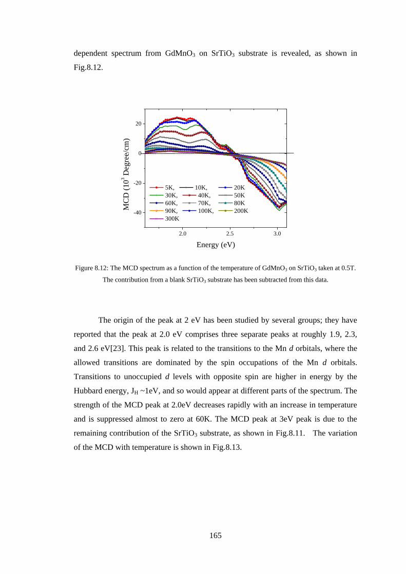
165
dependent spectrum from GdMnO3 on SrTiO3 substrate is revealed, as shown in
Fig.8.12.
2.0 2.5 3.0
-40
-20
0
20
MC
D (
10
3 D
egre
e/cm
)
Energy (eV)
5K, 10K, 20K
30K, 40K, 50K
60K, 70K, 80K
90K, 100K, 200K
300K
Figure 8.12: The MCD spectrum as a function of the temperature of GdMnO3 on SrTiO3 taken at 0.5T.
The contribution from a blank SrTiO3 substrate has been subtracted from this data.
The origin of the peak at 2 eV has been studied by several groups; they have
reported that the peak at 2.0 eV comprises three separate peaks at roughly 1.9, 2.3,
and 2.6 eV[23]. This peak is related to the transitions to the Mn d orbitals, where the
allowed transitions are dominated by the spin occupations of the Mn d orbitals.
Transitions to unoccupied d levels with opposite spin are higher in energy by the
Hubbard energy, JH ~1eV, and so would appear at different parts of the spectrum. The
strength of the MCD peak at 2.0eV decreases rapidly with an increase in temperature
and is suppressed almost to zero at 60K. The MCD peak at 3eV peak is due to the
remaining contribution of the SrTiO3 substrate, as shown in Fig.8.11. The variation
of the MCD with temperature is shown in Fig.8.13.
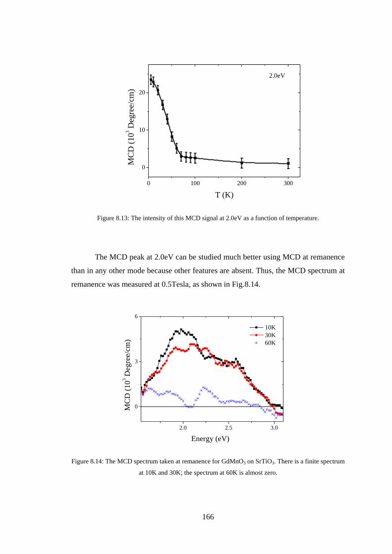
166
0 100 200 300
0
10
20
2.0eV
MC
D (
10
3 D
egre
e/cm
)
T (K)
Figure 8.13: The intensity of this MCD signal at 2.0eV as a function of temperature.
The MCD peak at 2.0eV can be studied much better using MCD at remanence
than in any other mode because other features are absent. Thus, the MCD spectrum at
remanence was measured at 0.5Tesla, as shown in Fig.8.14.
2.0 2.5 3.0
0
3
6
MC
D (
10
3 D
egre
e/cm
)
Energy (eV)
10K
30K
60K
Figure 8.14: The MCD spectrum taken at remanence for GdMnO3 on SrTiO3. There is a finite spectrum
at 10K and 30K; the spectrum at 60K is almost zero.
167
The MCD spectra in field (Fig.8.12) and in zero magnetic field (Fig.8.14) give
two optical features with different temperature and field dependencies. Usually, the
MCD spectrum measured in zero magnetic field has the same shape as the spectrum
measured in field but with lower magnitude. The MCD of GdMnO3 on SrTiO3 in field
and in zero magnetic field are not alike, which is a unique occurrence. The peak at
~2eV at 10K in the zero magnetic field spectrum has been reduced by a factor of ~5
relative to its value in field. Nonetheless, it is very surprising to obtain such a high
remanence spectrum at 30K. It is possible that the strain in the film induces a canted
phase already at TN. This peak at 2.0eV is due to a charge transfer excitation
between Mn ions and has been observed in the spectrum of LaMnO3 [21-23].
8.4 Conclusion
The optical and magneto-optical properties of an epitaxial film of GdMnO3
grown on SrTiO3 were investigated in order to obtain detailed information on the
magnetic polarisation of the electronic states. Two features in the optical spectrum,
well known from bulk studies, the charge transfer transition between Mn d states at
~2eV and the band edge transition from the oxygen p band to the d states at ~3eV,
were observed in the optical absorption and the magnetic circular dichroism (MCD).
The MCD peak at 2eV was not visible as a distinct peak in the absorption but showed
very clearly in the MCD spectrum, especially at remanence. The MCD at ~2eV
correlates well with the Mn spin ordering and the three peak structure observed in the
absorption spectrum of LaMnO3 also re-emerged and was observed in these data. The
MCD peak at 3eV is due to the STO substrate.

168
8.5 References
1. T. Lottermoser, T. Lonkai, U. Amann, D. Hohlwein, J. Ihringer and M. Fiebig,
Nature 430, 541-544 (2004).
2. N. Hur, S. Park, P.A. Sharma, J. S. Ahn, S. Guha and S. W. Cheong, Nature
429, 392-395 (2004).
3. T. Kimura, T. Goto, H. Shintani, K. Ishizaka, T. Arima and Y. Tokura, Nature
426, 55-58 (2003).
4. W. Prellier, M. P. Singh and P. Murugavel, J. Phys.: Condens. Matter 17,
R803 (2005).
5. R. Ramesh, and N. A. Spaldin, Nat Mater 6, 21-29 (2007).
6. F. Manfred, J. Phys. D: Appl. Phys. 38, R123 (2005).
7. N. Ikeda, H. Ohsumi, K. Ohwada, K. Ishii, T. Inami, K. Kakurai, Y.
Murakami, K. Yoshii, S. Mori, Y. Horibe and H. Kito, Nature 436, 1136-1138
(2005).
8. C. Ederer, and N. A. Spaldin, Current Opinion in Solid State and Materials
Science 9, 128-139 (2005).
9. D. G. Schlom, J. H. Haeni, J. Lettieri, C. D. Theis, W. Tian, J. C. Jiang and X.
Q. Pan, Mater. Sci. Eng. B 87, 282-291 (2001).
10. N. A. Spaldin, and M. Fiebig, Science 309, 391-392 (2005).
11. T. Goto, T. Kimura, G. Lawes, A. P. Ramirez and Y. Tokura, Phys. Rev. Lett.
92, 257201 (2004).
12. T. Kimura, G. Lawes, T. Goto, Y. Tokura and A.P. Ramirez, Phys. Rev. B 71,
224425 (2005).
13. W. S. Choi, D. G. Kim, S. S. A. Seo, S. J. Moon, D. Lee, J. H. Lee, H. S. Lee,
D. Y. Cho, Y. S. Lee, P. Murugavel, J. Yu and T. W. Noh, Phys. Rev. B 77,
045137 (2008).
14. M. Fiebig, T. Lottermoser, D. Frohlich, A. V. Goltsev and R. V. Pisarev,
Nature 419, 818-820 (2002).
15. J. Baier, D. Meier, K. Berggold, J. Hemberger, A. Balbashov, J. A. Mydosh
and T. Lorenz, J. Magn. Magn. Mater. 310, 1165-1167 (2007).
16. J. Baier, D. Meier, K. Berggold, J. Hemberger, A. Balbashov, J. A. Mydosh
and T. Lorenz, Phys. Rev. B 73, 100402 (2006).
169
17. K. Noda, S. Nakamura, J. Nagayama and H. Kuwahara, J. Appl. Phys. 97,
10C103 (2005).
18. J. Hemberger, S. Lobina, H. A. Krug von Nidda, N. Tristan, V. Y. Ivanov, A.
A. Mukhin, A. M. Balbashov and A. Loidl, Phys. Rev. B 70, 024414 (2004).
19. Y. Okimoto, Y. Konishi, M. Izumi, T. Manako, M. Kawasaki and Y. Tokura,
J. Phys. Soc. Jpn. 71, 613
20. Y. Konishi, Z. Fang, M. Izumi, T. Manako, M. Kasai, H. Kuwahara, M.
Kawasaki, K. Terakura and Y. Tokura, J. Phys. Soc. Jpn. 68, 3790
21. M. W. Kim, S. J. Moon, J. H. Jung, J. Yu, S. Parashar, P. Murugavel, J. H.
Lee and T.W. Noh, Phys. Rev. Lett. 96, 247205 (2006).
22. M. W. Kim, P. Murugavel, S. Parashar, J. S. Lee and T. W. Noh, New J. Phys.
6, 156 (2004).
23. M. Bastjan, S. G. Singer, G. Neuber, S. Eller, N. Aliouane, D. N. Argyriou, S.
L. Cooper, Uuml and M. Bhausen, Phys. Rev. B 77, 193105 (2008).
24. X. L. Wang, D. Li, T. Y. Cui, P. Kharel, W. Liu and Z. D. Zhang, J. Appl.
Phys. 107, 09B510 (2010).
25. K.V. Benthem, C. Elsasser and R. H. French, J. Appl. Phys. 90, 6156-6164
(2001).
26. M. A. Geday, and A. M. Glazer, J. Phys.: Condens. Matter 16, 3303 (2004).
170
Chapter 9 - Conclusions
9.1 Thesis Review
This study investigated the optical and magneto-optical properties of pure and
transition metal doped In2O3 in order to find a suitable material for the new generation
of spin-based electronics. In2O3 (IO) was chosen for the excellent combination of
magnetism, transport, optical and magneto-optical properties it has when doped with
Sn and transition metal.
Optical systems were developed to achieve a high accuracy, with low noise
level in addition to managing the low temperature measurements. Python, C++,
Microsoft.Net and LabView program were used to build up drivers to control the two
optical systems, and to acquire the data. Software was programmed to analyse the
obtained data. The absorption system was rebuilt in order to manage low temperature
measurements where new items, such as temperature controller, cryostat, vacuum
pump, were added to the system and new drivers were programmed to control the
temperature controller through the computer. Without these developments, obtaining
the optical and magneto-optical data seen in this study would have not been possible.
These systems were used to perform the first optical and magneto-optical
measurements on pure and doped In2O3 thin films. The optical and magneto-optical
properties of pure and (Cr, Mn, Fe, Co, Ni, Sn)-doped In2O3 were investigated at
different transition metal concentrations and at different growth conditions. However,
only selective and representative data have been included in this study. This study is
considered the first attempt that investigated the optical and magneto-optical
properties of pure and transition metal doped In2O3. The optical and magneto-optical
measurements showed that there was a group of energy states formed within the
forbidden range of the optical band gap energy of In2O3 and located closed lower the
conduction band. The origin of these states was found to be due to the defect states
associated with oxygen vacancies as confirmed by the absorption measurements at
low temperature. The density of the oxygen vacancy impurity states increases and
expands to a deeper level of energy toward the valance band with a decrease in
oxygen partial pressure during the growth, or with doping with tin, or with annealing

171
in a vacuum. Tuning the density of the oxygen vacancy impurity states gives control
over the carrier concentration density in the system. This achievement of controlling
the carrier concentration density leads the In2O3 semiconductor to show insulator or
metallic behaviours.
Magnetometry and the magneto-optical measurements of transition-metal doped
In2O3 revealed the origin of the magnetism in the class of the magnetic oxides. The
observed ferromagnetism in magnetic oxides was due to the polarized electrons in
localized donor states associated with oxygen vacancies.
Extended X-ray Absorption Fine Structure (EXAFS) measurements showed that
some of the transition-metal doped In2O3 thin films contain transition metal
nanoparticles. In this study, a new complementary technique to the EXAFS was
developed to identify the existence of magnetic nanoparticles in addition to providing
the fraction and contribution of these nanoparticles to the magnetisation and magneto-
optical properties. The Maxwell-Garnett analysis of magnetic circular dichroism was
developed to obtain quantitative measures of the amount of defect phases present for
Co metal. Similar to Maxwell-Garnett analysis, a new equation for Fe3O4
nanoparticles was developed in this study. The magneto-optical method is cheaper
where there is no cyclotron system required, safer where there is no involvement with
X-ray radiation, quantitative, and more accurate than the EXAFS method.
The fraction of transition metal nanoparticles was found to decrease with doping
with tin whereas metallic Co nanoparticles in Co-doped In2O3 thin films and Fe3O4
nanoparticles in Fe-doped In2O3 thin films disappeared when these thin films were
doped with tin indicating that doping with Sn not only introduces more carriers but
also inhibits the growth of defect phases in semi magnetic semiconductor thin films.
This might be because of screening from the carriers as a side effect of changing the
crystal strain as a result of doping with Sn.
9.2 Future Work
Completion of the current work on (Cr, Mn, Ni, Zn)-doped In2O3 is necessary
to have a comprehensive overview about the properties of transition metal doped
172
In2O3, and to be more confident about the source of magnetisation in semi magnetic
semiconductors. More measurements need to be done, including an accurate
assessment of the composition of thin films, and the percentage of spin polarisation
using an Andreev reflection and whether there are second phases or transition metal
nanoparticles present using extended X-ray absorption fine structure EXAFS
measurements.
It would be really interesting to grow two thin films, one pure In2O3, and one
transition metal doped In2O3, with the same carrier concentration or with the same
oxygen vacancy density which could be measured through the absorption spectra to
assess whether they show the same magnetic and magneto-optical properties in order
to determine the role of the transition metal itself in semi magnetic semiconductors.
We believe that role of the transition metal in semi magnetic semiconductors
is simply to cause an imbalance in the density of polarized carriers in oxygen vacancy
bands, which leads to a positive or a negative magnetic circular dichroism signal,
where Cr- , Fe-, and Co-doped In2O3 show a positive magnetic circular dichroism
signal, while Ni-doped In2O3 shows a negative magnetic circular dichroism signal. In
fact, we tried to investigate Zn-doped In2O3 to check this point, but we faced some
difficulties which delayed the project. However, the difference between the densities
of the polarized carriers in oxygen vacancy bands is responsible for the magnetisation
in semi magnetic semiconductors, which indeed needs to be investigated in the future.
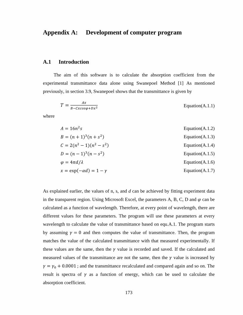
173
Appendix A: Development of computer program
A.1 Introduction
The aim of this software is to calculate the absorption coefficient from the
experimental transmittance data alone using Swanepoel Method [1] As mentioned
previously, in section 3.9, Swanepoel shows that the transmittance is given by
𝑇 = 𝐴𝑥𝐵−𝐶𝑥𝑐𝑜𝑠𝜑+𝐷𝑥2
Equation(A.1.1)
where
𝐴 = 16𝑛2𝑠 Equation(A.1.2)
𝐵 = (𝑛 + 1)3(𝑛 + 𝑠2) Equation(A.1.3)
𝐶 = 2(𝑛2 − 1)(𝑛2 − 𝑠2) Equation(A.1.4)
𝐷 = (𝑛 − 1)3(𝑛 − 𝑠2) Equation(A.1.5)
𝜑 = 4𝜋𝑑/𝜆 Equation(A.1.6)
𝑥 = exp(−𝛼𝑑) = 1 − 𝛾 Equation(A.1.7)
As explained earlier, the values of n, s, and d can be achieved by fitting experiment data
in the transparent region. Using Microsoft Excel, the parameters A, B, C, D and 𝜑 can be
calculated as a function of wavelength. Therefore, at every point of wavelength, there are
different values for these parameters. The program will use these parameters at every
wavelength to calculate the value of transmittance based on equ.A.1. The program starts
by assuming 𝛾 = 0 and then computes the value of transmittance. Then, the program
matches the value of the calculated transmittance with that measured experimentally. If
these values are the same, then the 𝛾 value is recorded and saved. If the calculated and
measured values of the transmittance are not the same, then the 𝛾 value is increased by
𝛾 = 𝛾0 + 0.0001 ; and the transmittance recalculated and compared again and so on. The
result is spectra of 𝛾 as a function of energy, which can be used to calculate the
absorption coefficient.
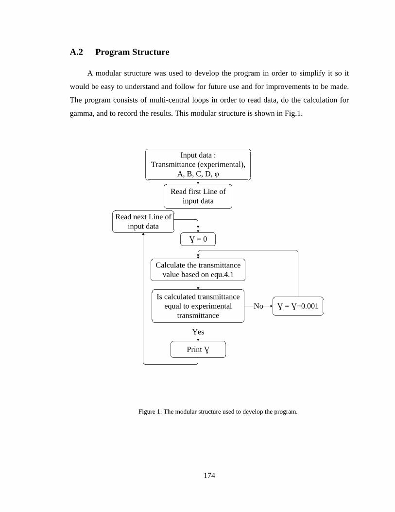
174
A.2 Program Structure
A modular structure was used to develop the program in order to simplify it so it
would be easy to understand and follow for future use and for improvements to be made.
The program consists of multi-central loops in order to read data, do the calculation for
gamma, and to record the results. This modular structure is shown in Fig.1.
Input data :Transmittance (experimental),
A, B, C, D, φ
Read first Line of input data
Calculate the transmittance value based on equ.4.1
Is calculated transmittance equal to experimental
transmittance
Ɣ = 0
Print Ɣ
Yes
Read next Line of input data
Ɣ = Ɣ+0.001No
Figure 1: The modular structure used to develop the program.
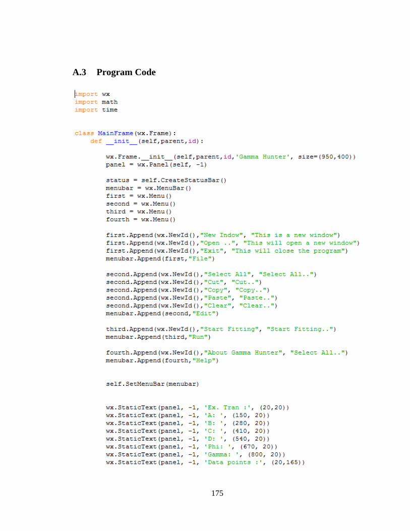
175
A.3 Program Code
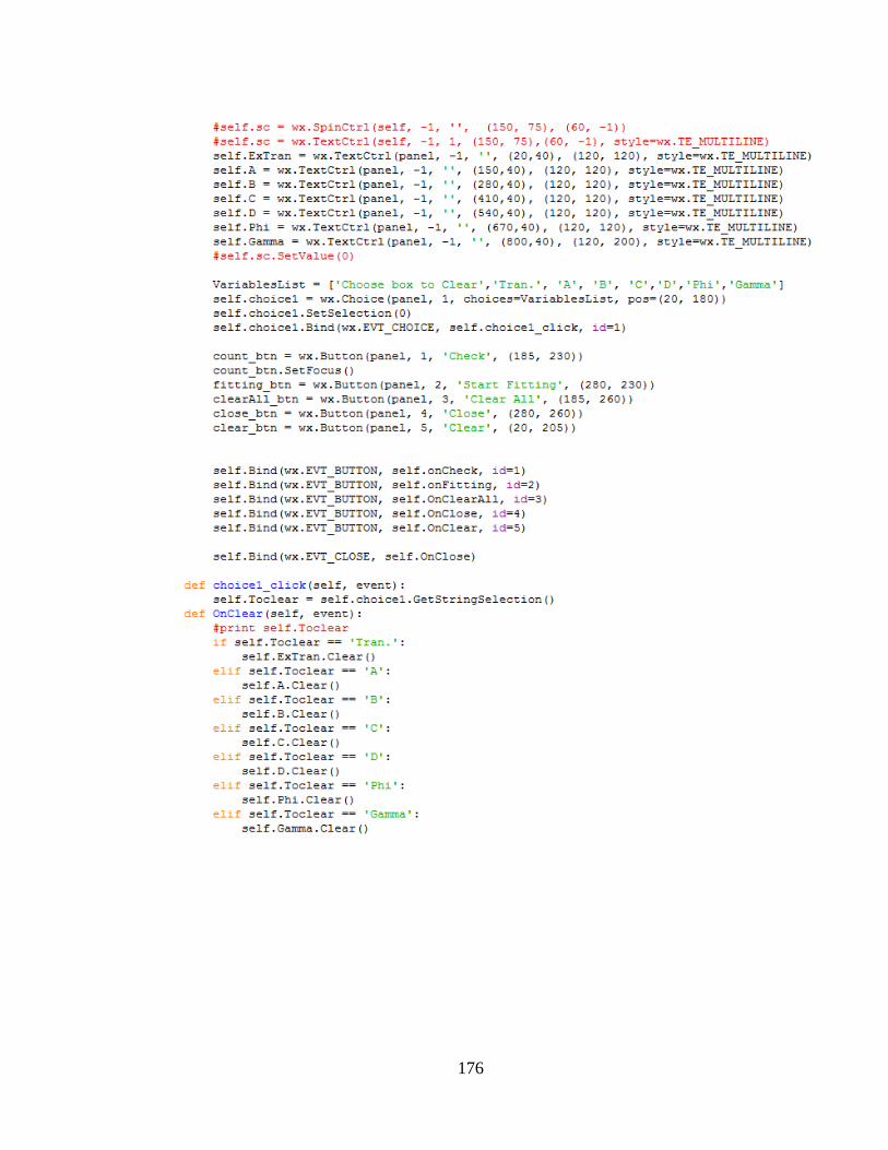
176

177

178
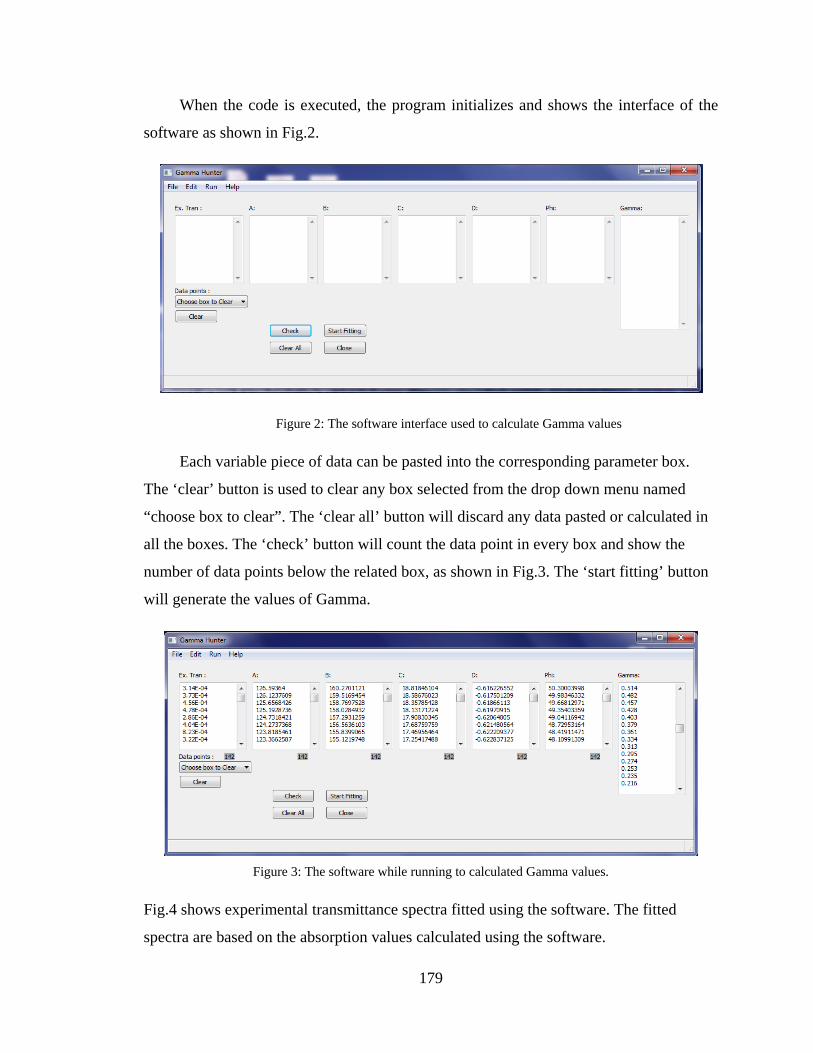
179
When the code is executed, the program initializes and shows the interface of the
software as shown in Fig.2.
Figure 2: The software interface used to calculate Gamma values
Each variable piece of data can be pasted into the corresponding parameter box.
The ‘clear’ button is used to clear any box selected from the drop down menu named
“choose box to clear”. The ‘clear all’ button will discard any data pasted or calculated in
all the boxes. The ‘check’ button will count the data point in every box and show the
number of data points below the related box, as shown in Fig.3. The ‘start fitting’ button
will generate the values of Gamma.
Figure 3: The software while running to calculated Gamma values.
Fig.4 shows experimental transmittance spectra fitted using the software. The fitted
spectra are based on the absorption values calculated using the software.

180
Figure 4: Transmittance spectra fitted using the software.
2.0 2.5 3.0 3.5 4.0 4.50.0
0.2
0.4
0.6
0.8
1.0
Tran
smitt
ance
(%)
Energy (eV)
10K Fitting

181
A.4 References
1. R. Swanepoel, J. Phys. E: Scientific Instruments, 1983. 16(12): p. 1214.

182
Appendix B: Abbreviations
CB Conduction band
CL Cathodoluminescence spectra
DL Deep-level states
DMSs Dilute magnetic semiconductors
EDAX Energy-dispersive X-ray spectroscopy
EF Fermi energy level
EXAFS X-ray absorption fine structure
GPIB General Purpose Interface Bus
Hc Coercive field or coercively
ITO Indium-tin-oxide
KACST King Abdulaziz City for Science and Technology
LabVIEW Laboratory Virtual Instrumentation Engineering Workbench
LCD Liquid crystal display
LCP Left circularly polarized light
MAX The Measurement and Automation
MBE Molecular beam epitaxy
MCD Magnetic circular dichroism
M-G Maxwell-Garnett theory
Mr Remaining magnetization, or remanence
Ms Saturation magnetization
NBE Near-band-edge states
OLED Organic light emitting diode
PLD Pulse laser deposition
RCP Right circularly polarized light
RKKY Ruderman-Kittel-Kasuya-Yosida model
SMS Semi magnetic semiconductors
SQUID Superconducting quantum interference device
TC Curie temperature
TM Transition element

183
TN Néel temperature
VB Valence band
XMCD X-ray magnetic circular dichroism
XRD X-ray diffraction