accurate static timing analysis for deep submicronic cmos ...accurate static timing analysis for...
TRANSCRIPT

36
Accurate static timing analysis for deep submicronic CMOS circuits
Karim Dioury, Alain Greiner; Marie-Minerve Rosset-Loui!rat Laboratoire d'lnformatique de Paris 6 (LIP6), Universite Pierre et Marie Curie Couloir 55-65, 210, 4 place Jussieu, 75252 Paris Cedex 05, FRANCE, telephone:(33) 1 44 27 30 43, Fax:(33) 1 44 27 72 80, e-mail: Marie-Minerve.Louerat@ lip6jr
Abstract This paper presents the performance of the static timing analyzer TAS for deep submicronic CMOS technologies. The methodology used by TAS is given with special emphasis on its Short Channel MOS model. Results are given to show the accuracy of the static timing analyzer TAS for various CMOS circuits (including pass transistor and precharge logic) as well as for various CMOS processes ranging from 1.2J.t to 0.35J.t. The Short Channel MOS model of TAS appears to be relevant to the analysis of deep submicronic processes.
Keywords Static timing analysis, verification, VLSI CAD, performance
1 INTRODUCTION
The timing analysis problem, on a synchronous sequential logic circuit where each register is enabled by a single clock, is to find out the lowest clock period at which the circuit operates correctly. This problem is solved in two main phases : a functional analysis of the sequential behavior (disassembling phase, timing independent) followed by a timing dependent analysis of the combinational behavior (SangiovanniVincentelli et al. 1996).
The various types of models describing the timing behavior of CMOS circuits demonstrate the compromise between simulation accuracy and simulation expense (Wunder et al. 1996).
Dynamic electrical simulation that solves nonlinear transistor differential equations like SPICE (Nagel 1975) or ELDO (Anacad 1996) are often considered to be impracticable because of the computation time (Cheng et al. 1992, SangiovanniVincentelli et al. 1996, Wunder et al. 1996) and yet it is the only acknowledged reference for timing specifications of a circuit before foundry.
Static timing analyzers (Ousterhout 1985) are well known to bring a less accurate but practicable solution to the analysis problem. Their ability to handle much larger
YLSI: Integrated Systems on Silicon R. Reis & L. Claesen (Eds.) e lAP 1997 Published hy Chapman & Hall

440 Part Ten Physical Design Issues in Sub-micron Technologies
circuits results from the use of a pattern independent approach, together with simpler models of gate delays. They exploit the unidirectional flow in MOS circuits.
Existing commercial timing analysis tools (Schulz 1995) like Cadence, Compass, Chronology, EPIC, Mentor Graphics, Synopsys and ViewLogic use different approaches regarding the type of analysis performed (static or dynamic), the input netlist (transistor level, gate level or R1L level) and the type of timing model of the considered devices (RC model of the transistor, nonlinear equation table, nonlinear model of the transistor, nonlinear table of gate commutation). Very few perform static timing analysis on transistor level netlists with a nonlinear model of the transistor (only EPIC does).
Currently the complexity of large circuits can reach several million transistors. Designing such circuits requires the use of decomposition into megablocks of 10k-50k transistors followed by connection of the blocks to produce the complete design. Like Epic (Schulz 1995) we assume that transistor level static timing analysis is performed on each of the megablocks. Then the analysis is performed at higher levels following the hierarchical approach used for the design. Here we concentrate on the analysis of each individual megablocks.
TAS is a transistor level static timing analyzer for CMOS circuits (Hajjar et al. 1991) and takes a post layout SPICE netlist as input. It brings an original and accurate solution to characterization of complex Asics. The speeding up relies on the underlying gate structure of any digital CMOS circuit. The transistor netlist is automatically partitioned into a directed gate netlist. Each gate is then characterized taking into account signal slopes and reduced to an equivalent inverter. The computation of the delays uses the original TAS Short Channel MOS (TSCM) model of the transistor. In order to detect critical paths, TAS makes 'worst case' timing assumptions (Ousterhout 1985). The initial implementation of TAS was developed by Hajjar et al. (1991). It worked together with the gate abstractor DESB (Greiner et al. 1992). Its performance was evaluated on CMOS circuits for a technology larger than 1/L. Now TAS works with another gate abstractor called YAGLE (Lester 1994) that allows the disassembling of much larger circuits than DESB, as well as special circuitry. Results are given here to show the accuracy of TAS for various CMOS circuits (including pass transistor and precharge logic) as well as for various CMOS processes ranging from 1.2/l to 0.35p. The Short Channel MOS model of TAS appears to be relevant to analyze deep submicronic processes since most of TAS results are within 5% versus the SPICE ones.
The paper is organized as follows: Section 2 introduces the main principles of TAS. Section 3 validates previous assumptions on a representative set of CMOS circuits by comparisons with SPICE simulations.
2 TAS PRINCIPLES
TAS works on a SPICE netlist obtained by a classical layout extractor. The analysis is based on analytical equations that take into account the following factors:

Accurate static timing analysis for deep submicronic CMOS circuits 441
• The current versus voltage characteristics of Short Channel Mosfets are modeled with nonlinear equations.
• The signal slopes effects, that is commutation time of input signal (Auvergne et al. 1990, Dagenais et al. 1992) are computed with an RC model.
• The transient short circuit current during the commutation of a gate (Turgis et al. 1997) is approximated to an additional load capacitance, called here the conflict capacitance.
Exhaustive analysis of all paths that may be sensitized is performed in order to find the resulting worst possible timing behavior.
TAS works on a post layout transistor level netlist. The first main phase of the analysis is timing independent. It consists in extracting the functionality of the netlist. It is performed in two steps, the first is the disassembling phase to build a gate netlist (section 2.1 ), it is followed by the construction of the graph considering the possible transitions of signals (section 2.2). The second main phase is timing dependent. It consists in the computation of gate delays (section 2.3), followed by the determination of the longest and shortest paths (section 2.4).
2.1 The gate netlist
From the extracted transistor netlist, a 'pseudo gate' netlist is built according to the algorithm used in the partitioning tool YAGLE (Lester 1994):
• Each signal Y driving a transistor gate is the output of a single gate. • The gate labeled Y is the collection of electrical paths between Y and the supplies
(power or ground). • There are two kinds of paths. The UP paths from Y to Vvv (power supply) and
the DOWN paths from Y to Vss (ground supply). • A path is thus made of series connected transistors. Such a path is also called a
branch. It is similar to the stage structure introduced by Ousterhout (1985) in his timing verifier CRYSTAL, for CMOS circuits.
The transistor orientation is also solved by YAGLE. Therefore a gate is oriented, has one output and several inputs and is made of several branches. A first graph is built (dependence graph) with false branch elimination (non functional) where:
• the nodes are the signals; • the oriented edges are the dependences between signals (existence of a gate input
output relationship).

442 Part Ten Physical Design Issues in Sub-micron Technologies
2.2 The causality graph
From this first graph TAS builds the causality graph :
• A node is one of the two possible events associated to a signal (LOW-HIGH transition and HIGH-LOW transition). Hence, each node of the first graph will make two nodes in the causality graph.
• An oriented edge exists between two nodes if the transition of the output node can be actually driven by the transition of the input node (for an inverting gate there are only two possible edges, for XOR gates there are four edges).
2.3 The gate delay computation
From the causality graph, TAS builds the event graph by computing the propagation delay between two nodes in two steps :
I. First TAS performs a local evaluation of the input slopes. This is done by ignoring the coupling effect of the actual switching input and by using a simple RC model of the transistors to evaluate locally the worst case commutation time of the gate output. To each node i of the event graph is thus associated an intrinsic slopeS,, depending only on :
• The geometry of the gate which has node i as an output. • The equivalent capacitive load on node i, Ci that takes into account the drain
capacitances that can be discharged, the gate capacitances of the transistors having i as an input - including those seen through pass transistors -, the post layout capacitances of the wires connected to node i.
2. Second, TAS computes the gate delay associated with each edge in this graph. For each couple (input,output) TAS creates a set of branches associated with the output by looking at all the branches found by the disassembling that have the same input and output. TAS assumes that only a single transistor is turning on or off at once. This a popular assumption in the area of delay modeling of gates, however studies begin on the case of multiple input switching in close temporal proximity (Chandramouli et al. 1996). To set the state of the other transistors belonging to the switching gate, TAS finds the combination of values that results in the worst possible timing behavior, that is the worst case assumption used by Ousterhout (1985) and Dagenais et al. (1992). Then TAS reduces the branches to a unique inverter - the equivalent inverter -by analyzing the maximum current that can flow during the switching. The TAS
Accurate static timing analysis for deep submicronic CMOS circuits 443
original Short Channel MOS model (TSCM) introduced by Haijar et al. ( 1991) is used . In this model the drain current of aMOS transistor is expressed as follows :
sub threshold mode :
Vas< VT linear mode :
Vvs < VsAT saturation mode :
Vvs > VsAT saturation voltage :
l= 0;
I= Vvs/RT;
I sAT = A(Vas- VT )2 /(1 + B(Vas- VT ));
VsAT = K(Vas- VT) with 0 < K < 1.
(1)
where VT is the threshold voltage, VsAT the saturation voltage, A and B are the transconductance parameters in the saturation region, RT the resistance in the linear mode. The parameters in the TSCM model are generated by running SPICE simulations on simple fitting circuits, made of simple branches (Dioury et al. 1997) : Figures 1 and 2 show the static characteristics of the N MOS transistor for the TSCM model and the SPICE level 3 model for a 0.8 JL technology. Figures 3 and 4 show the same for the P MOS. The TSCM model is simpler than the one studied by Sakurai et al. (1990), yet it is also well fitted to take into account the particular effect of short channel transistor like the carrier's velocity (Sakurai et al. 1991 ). The equivalent inverter is then passed to a delay modeler that computes how long it will take for the output of the branch to change value. The delay modeler uses the TSCM model to compute the time interval between the time when the input irises Vvv/2 and the time the the output j rises Vvv/2. The delay ti,j depends on:
• The slope on node i, si . • The geometry of the gate which has node j as output. • The equivalent capacitive load on node j, Cj. It is modeled like the above
mentioned Ci for slope computation, with addition of the conflict capacitance.
In the following we give more details on computing ti,j. We approximate signal waveforms by an hyperbolic tangent function (Haijar 1992), the input signal on node i is expressed by :
t < 0 ~ v < VT t > 0 ~ v = VT + (Ui- VTth(t/Si))
(2)
where: Si is the slope on node i and Ui is the maximum voltage reached by the input. Usually it equals Vvv except when the input is controlled by a pass transistor.

444 Part Ten Physical Design Issues in Sub-micron Technologies
Then the high to low delay t~l from input i to output j discharging the equivalent capacitance C; is computed under the assumption that when the output j goes from VDD to VDD/2 the current IMAx(t) driving C; can be approximated using equation I - saturation mode - and equation 2 where A, B, Si and Ui are replaced by A', B', S~ and Uf to model the series connected transistors in the switching branch (Ha.ijar 1992). The resulting equation is:
(3)
when the transistor operates in the saturation mode the drain current I MAX ( t) depends only on Vas as in equation I. Combining equations I, 2 and 3 gives:
1x A'.U?th2(tfS;)f(l + B'.UI.th(tfSD).dt = Q = 0.5C;VDD (4)
The delay, that has been defined as the time interval between the instant when the input i reaches VDD/2 and the instant when the output j reaches VDD/2, is derived through an iterative process from the solution X of equation 4 by :
t~/ = X- Argth(0.5VDD/Uf)
~0014
mllllldd-
~ll ......... -
~I
o.tlXll
IDS (A)
II.IXXII
l 3 4 4..! VDS(V)
Figure 1 Drain current versus voltage I(VDs) for Vas = 4.5V of the TSCM model (NMOS) compared with the Spice level 3 model, for a 0.8 I' technology
(5)
~14
~ll
QOOI
O.IXXI
IDS(A)
O.IXlli
G.llXN
~IIXI2
l 3 4 4.! VGS(V)
Figure 2 Saturation current versus voltage !(Vas) of the TSCM model (NMOS) compared with the Spice level 3 model, for a 0.8 I' technology

Accurate static timing analysis for deep submicronic CMOS circuits 445
OJXl12 ma:ooodcl-
.p..nldel-QOOI
0.00111
IDS(A)O.Imi
0.11Xl4
2 J 4 4j VllS(V)
Figure 3 Drain current versus voltage I(VDs) for Vas = 4.5V of the TSCM model (PMOS) compared with the Spice level 3 model, for a 0.8 JL technology
2.4 Static timing analysis
0.0012
QOOI
0.00111
IDS(A)O.IIXli
0.11Xl4
O.IXXJ2
ma;ooodcl.po:ooodcl-·-
2 J 4 4.l VGS(V)
Figure 4 Saturation current versus voltage !(Vas) of the TSCM model (PMOS) compared with the Spice level 3 model, for a 0.8 JL technology
TAS analyses the event graph to give the worst case delay between all circuit terminals (input connector, output connector or internal register). It is done by using a backward breadth-first algorithm to find both the longest and the shortest paths between two terminals.
hierarchical netlist
with interconnections
Figure 5 Flow graph of the timing analysis
The design of multi-million transistor chip uses decomposition, which consists of breaking the design at a given level of hierarchy into components that can be designed and verified almost independently. No timing analyzer can handle very
446 Part Ten Physical Design Issues in Sub-micron Technologies
complex circuits without the use of decomposition. The aim of the analysis made here is to handle the leaf block level of the hierarchy to be used by a hierarchical analyzer later (see Figure 5). In order to be fast enough we have chosen not to make a priori false path detection (Perremans et al. 1989, Benkoski eta/. 1990), but to leave this detection for the detailed analysis of single paths if needed.
3 RESULTS
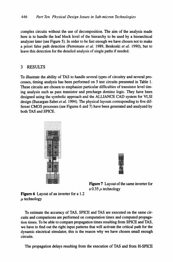
To illustrate the ability of TAS to handle several types of circuitry and several processes, timing analysis has been performed on 5 test circuits presented in Table 1. These circuits are chosen to emphasize particular difficulties of transistor level timing analysis such as pass transistor and precharge domino logic. They have been designed using the symbolic approach and the ALLIANCE CAD system for VLSI design (Bazargan-Sabet eta/. 1994 ). The physical layouts corresponding to five different CMOS processes (see Figures 6 and 7) have been generated and analyzed by both TAS and SPICE.
Figure 6 Layout of an inverter for a 1.2 J.l technology
Figure 7 Layout of the same inverter for a 0.35 J.l technology
To estimate the accuracy of TAS, SPICE and TAS are executed on the same circuits and comparisons are performed on computation times and computed propagation times. To be able to compare propagation times resulting from SPICE and TAS, we have to find out the right input patterns that will activate the critical path for the dynamic electrical simulator, this is the reason why we have chosen small enough circuits.
The propagation delays resulting from the execution of TAS and from H-SPICE

Accurate static timing analysis for deep submicronic CMOS circuits 447
Table 1 Description of the circuit benches for comparison of TAS versus spice
Circuit Function Size of operands: Main feature (Number of number of bits of the design transistors) (reference)
alu arithmetical 4 DUAL CMOS (434) logical unit (AMD 1977)
rsa fast adder 4 xor with bleeder (117) (Lucas et al. 1993)
grog rom 64 words precharge domino logic (368) *I bit (Greineretal. 1994)
amg multiplier 6 complex CMOS cells (1114) (Royannez et al. 1994)
bsg barrel 4 N MOS pass transistors (270) shifter (Bazargan-Sabet et al. 1994)
(by Meta-Software) simulation are shown on Table 2. The error in TAS is defined as:
lOO(tas- spice)fTAS (6)
In most of the cases, the results of TAS are within 7 percent versus SPICE. This shows that the TSCM model is relevant for a large range of deep submicronic technologies. The worst results are obtained with the multiplier. Yet the multiplier 'amg' includes some complex CMOS cells as :
a or (band c) or ((nota) and (not b) and (note) (7)
TAS is pessimistic for complex cells because for a given input to output delay, it takes the worst case assumption regarding the other input patterns .
TAS is must faster than SPICE. For example simulation of the multiplier 'amg' lasts 30 minutes with SPICE and 2 seconds with TAS.
TAS has also been successfully used on high complexity circuits. The largest example studied with TAS with a decomposition approach, is AURIGA2 from BULL. AURIGA2 is a control processor unit on one chip, made of 4.7 million transistors with a CMOS 0.51' 3 metal technology. The most interesting result is that TAS has been able to classify the electrical paths of the chip, regarding the commutation time.

448 Part Ten Physical Design Issues in Sub-micron Technologies
Table 2 Critical paths (ns) of various circuits versus technology feature size
Circuit Technology Voltage supply SPICE TAS error feature size (p,m) (V) (ns) (ns)
0.35 3.0 3.12 3.11 -0.3 alu 0.5 3.0 7.35 7.59 +3.0
0.8 4.5 8.58 8.58 0 1.0 4.5 9.80 10.3 +4.5 1.2 4.5 16.2 15.8 -2.0
0.35 3.0 1.7 1.8 +5.5 rsa 0.5 3.0 3.76 4.02 +6.0
0.8 4.5 4.33 4.41 +2.0 1.0 4.5 5.02 5.50 +8.5 1.2 4.5 8.15 8.29 +1.5
0.35 3.0 3.45 3.78 +8.5 amg 0.5 3.0 7.75 8.48 +8.6
0.8 4.5 8.83 9.20 +4.0 1.0 4.5 9.96 11.1 +10.0 1.2 4.5 17.0 18.0 +5.5
0.35 3.0 9.9 10.1 +2 bsg 0.5 3.0 2.01 1.95 -3.0
0.8 4.5 2.32 2.17 -7.0 1.0 4.5 2.44 2.54 +4.0 1.2 4.5 3.76 3.72 -1.0
0.35 3.0 1.89 2.04 +7.0 grog 0.5 3.0 3.50 3.70 +5.0
0.8 4.5 4.14 3.96 -4.5 1.0 4.5 4.87 5.12 +5.0 1.2 4.5 7.89 7.73 -2.0
4 CONCLUSION AND FUTURE WORK
TAS is a static timing analyzer that gives accurate timing information for high complexity Asics. The analysis achieved by TAS with the TSCM model is relevant for optimized design using a wide range of submicronic technologies . It works successfully on the leaf cell level of the hierarchy of high complexity circuits (millions of transistors).
Our efforts now concern the hierarchical analysis as shown in Figure 5 taking into account the resistances of interconnections.

Accurate static timing analysis for deep submicronic CMOS circuits 449
5 ACKNOWLEDGMENT
The authors thanks BULL for using TAS intensively and specially on high complexity circuits such as AURIGA2. Special thanks to Marcelo Duhalde.
REFERENCES
Advanced Micro Device (1977) Data sheet of the amd290 1. Anacad- Mentor Graphics Inc. (1996) Eldo User's Manual. Auvergne, D. , Azemard, A. , Deschacht, D. and Robert, M. (1990) Input waveform
slope effects in CMOS delays.JEEE J. of Solid-State Circuits, 25, 1588-3. Bazargan-Sabet, P., Burgun, L., Greiner, A. and Petrot, F. (1994) Methodology and
development of a complete CAD system for digital VLSI design, in Proc. Vlll Simposio Brasileiro de Concepcao de Circuitos lntegrados, Gramado, 11-5.
Benkoski, J., Vanden Meersch, E., Claesen, L.J.M. and De Man, H. (1990) Timing verification using statically sensitizable paths. JEEE Trans. on ComputerAided Design, 9, 1073-12.
Chandramouli, V. and Sakallah, K.A. (1996) Modeling the effects of temporal proximity of input transitions on gate propagation delay and transition time, in Proc. 33rd Design Automation Conference, Las Vegas.
Cheng, S.W. , Chen, H.C. , Du, D.H.C. and Lim, A. (1992) The role of long and short paths in circuit performance optimization, in Proc. ACM/JEEE Design Automation Conference, Anaheim, 543-6.
Dagenais, M.R., Gaiotti, S. and Rumin, N.C. (1992) Transistor-level estimation of worst case delays in MOS VLSI circuits. JEEE Trans. on Computer-Aided Design, 11,384-12.
Dioury, K. and Rosset-Louerat, M.-M. (1997) Fitting the technoly file for the static timing analyser TAS. LIP6, Universite Pierre et Marie Curie, Paris.
Greiner, A., Laurentin, M. and Marbot, R. (1992) DESB, a functional abstractor for CMOS VLSI circuits, in Proc. European Design Automation Conference, Hamburg, 22-6.
Greiner, A. and Petrot, F. (1994) A public domain high performances portable ROM generator, in Proc. 20th Euromicro, Liverpool, 414-6.
Hajjar, A. , Marbot, R. , Greiner, A. and Kiani. P. (1991) TAS : An accurate timing analyser for CMOS VLSI, in Proc. 2nd European Conference on Design Automation, Amsterdam, 261-6.
Hajjar, A. (1992) Modelisation des temps de propagation et analyse temporelle statique des circuits integres CMOS. PHD Thesis, Paris, Universite Pierre et Marie Curie.
Lester, A. (1994) YAGLE: Yet Another Gate Level Extractor. LIP6, Universite Pierre et Marie Curie, Paris.
Lucas, L. , Greiner, A. and Thill, M. (1993) High speed adder generator, in Proc. 5th lnternational Conference on Microelectronic, Dhahran, 136-4.

450 Part Ten Physical Design Issues in Sub-micron Technologies
Nagel, L.W. (1975) SP/CE2: A computer program to simulate semiconductor circuits. University of California, ERL Memo ERL-M520, Berkekey.
Ousterhout, J.K. (1985) A switch-level timing verifier for digital MOS VLSI. IEEE Trans. on Computer-Aided Design, CAD-4, 336-14.
Perremans, S. , Claesen, L. and De Man, H. (1989) Static timing analysis of dynamically sensitizable paths, in Proc. 26th ACM/IEEE Design Automation conference, 568-6.
Royannez, P., Greiner, A. and Amara, A. (1994) Booth multi-pipelined multiplier generator, in Proc. the IX Congressoda Sociedade Brasileira de Microelectronica (SBMICRO), Rio de Janeiro, 686-4.
Sakurai, T. and Newton, A.R. (1990) Alpha-power law MOSFET model and its applications to CMOS inverter delay and other formulas. IEEE J. of Solid-State Circuits, 25, 584-11.
Sakurai, T. and Newton, A.R. (1991) Delay analysis of series-connected MOSFET circuits IEEE J. of solid-state circuits, 26, 122-10.
Sangiovanni-Vincentelli, A.L., Me Geer, P.C. and Saldanha, A. (1996) Verification of electronic systems, in Proc. 33rd Design Automation Conference, Las Vegas.
Schulz, S .E. ( 1995) Timing analysis tools and trends. Integrated System Design Magazine, nov.
Turgis, S., Daga, J.M., Portal, J.M. and Auvergne, D. (1997) Internal power modelling and minimization in CMOS inverters, in Proc. The European Design & Test Conference, Paris, 603-6.
Wunder, B., Lehmann, G. and Miiller-Glaser, K.D. (1996) VAMP: a VHDL based concept for accurate modeling and post layout timing simulation of electronic systems, in Proc. 33rd Design Automation Conference, Las Vegas.
6 BIOGRAPHY
Karim DIOURY was born in Casablanca, Morocco, in 1969. He is currently preparing his PhD in the area of timing analysis for VLSI circuits. His research interest are timing analysis, interconnection and transistor modeling, clock and power supply tree design, VLSI design and CAD tools. Alain GREINER was born in Paris, France, in 1952. He is currently Professor at University Pierre et Marie Curie and the head of the Architecture Department at LIP6 laboratory. His main interests are in computer architecture, VLSI design, and CAD tools. Marie-Minerve ROSSET-LOUERAT was born in Paris, France, 1959. Since 1992 she has been with the LIP6-Architecture Department, as a permanent researcher. Her main interests are in low level CAD tools for digital and analog design.