acs764: fully integrated, hall-effect based current sensor...
TRANSCRIPT

NOTE: For detailed information on purchasing options, contact your local Allegro field applications engineer or sales representative.
Allegro MicroSystems, LLC reserves the right to make, from time to time, revisions to the anticipated product life cycle plan for a product to accommodate changes in production capabilities, alternative product availabilities, or market demand. The information included herein is believed to be accurate and reliable. However, Allegro MicroSystems, LLC assumes no respon-sibility for its use; nor for any infringements of patents or other rights of third parties which may result from its use.
Recommended Substitutions: no direct replacement
Fully Integrated, Hall-Effect Based Current Sensor ICWith I2C Digital Output and Low-Resistance Current Conductor
ACS764
For existing customer transition, and for new customers or new appli-cations, contact Allegro Marketing.
Date of status change: December 5, 2016
This device is no longer in production. The device should not be purchased for new design applications. Samples are no longer available.
Discontinued Product

DescriptionThe Allegro™ ACS764 fully integrated Hall-effect current sensor IC is designed for applications that require digital current sensing and reporting through an I2C™ bus. Allegro factory programming of the offset and gain, including the temperature coefficients, stabilizes the offset and gain over the operating temperature range. This programming greatly reduces the device total error, typically less than 2% over the operating temperature range. A fast response digital fault output is also provided. Both coarse sensitivity and fault level can be programmed via an I2C control register, and can be used for enhanced diagnostic functions.
The integrated low resistance conductor eliminates the requirement for external shunt resistors and, by employing Hall-effect sensing technology, eliminates the error associated with changing sense resistance due to temperature. The device allows 16 unique I2C bus addresses, selectable via external pins. The sensor IC gain can be selected by the user through the I2C bus. The device uses a BiCMOS process that allows a highly stable chopper-stabilized small signal amplifier design.
The ACS764 is provided in a compact 24-pin QSOP package (suffix LF). The leadframe is plated with 100% matte tin, which is compatible with standard lead (Pb) free printed circuit board assembly processes. Internally, the device is Pb-free, except for flip-chip high-temperature Pb-based solder balls, currently exempt from RoHS.
ACS764-DS
Features and Benefits• Fully integrated current sensor IC in a compact QSOP
package eliminates the need for shunt resistors• Hall effect sensing technology eliminates the error
associated with shunt resistor variation due to temperature• High accuracy: typical error < 2% over operating
temperature range• Fast response digital fault output with programmable level
through I2C bus interface• Digital output through I2C interface with 9-bit A-to-D
conversion for high resolution current measurement• User-selectable decimation averaging of current output; up
to 256 samples• Freeze pin for holding current measurement value while
reading many sensors serially• User-selectable (via I2C) coarse sensitivity and
OC fault levels, for exceptional flexibility to meet application requirements
Fully Integrated, Hall-Effect Based Current Sensor IC With I2C Digital Output and Low-Resistance Current Conductor
Package: 24-pin QSOP (suffix LF)
Typical Application Diagrams
Not to scale
ACS764
Continued on the next page…
IP
ACS764(I2C Slave)
VCC
+3.3 V
CBYP0.1 μF
RPU
VCC
VA1
1
2
3
4
5
6
7
8
9
10
11
12
24
23
22
21
20
19
18
17
16
15
14
13
IP+
IP+
IP+
IP+
IP+
IP+
IP+
VCC
SDA
SCL
GND
NC
IP–
IP–
IP–
IP–
IP–
IP–
IP–
A1
A0
FAULT
FREEZE
NC
VCC
VA0

Fully Integrated, Hall-Effect Based Current Sensor IC with I2C Digital Output and Low-Resistance Current ConductorACS764
2Allegro MicroSystems, LLC115 Northeast CutoffWorcester, Massachusetts 01615-0036 U.S.A.1.508.853.5000; www.allegromicro.com
Absolute Maximum RatingsCharacteristic Symbol Notes Rating Unit
Forward Supply Voltage VCC 7 V
Forward F A U ¯L T Pin Voltage VFAULT 24 V
DC Forward Voltage (A0, A1, FREEZE pins) VFDCx 7 V
DC Reverse Voltage (VCC, A0, A1, F A U ¯L T , FREEZE pins) VRDCx –0.5 V
Operating Ambient Temperature TA X temperature range –20 to 125 ºC
Maximum Junction Temperature TJ(max) 165 ºC
Storage Temperature Tstg –65 to 165 ºC
Selection Guide
Part Number Packing*Operating Ambient
Temperature,TA(°C)
Optimized Current Sensing
Range(A)
Optimized Nominal Resolution
(mA/LSB)
ACS764XLFTR-32AU-T Tape and reel, 2500 pieces/reel –20 to 125 32 62.62ACS764XLFTR-16AU-T Tape and reel, 2500 pieces/reel –20 to 125 16 31.31
*Contact Allegro™ for additional packing options.
• Less than 0.5 mΩ series resistance greatly reduces power dissipation and heat generation
• Factory programmed temperature compensation stabilizes sensitivity and offset voltage throughout the operating temperature range
• 16 programmable I2C addresses• Unidirectional DC current sensing and reporting• Immunity to stray magnetic fields simplifies PCB layout
Features and Benefits (continued)
Thermal CharacteristicsCharacteristic Symbol Test Conditions Value Unit
Steady State Package Thermal Resistance RθJA
Tested with 30 A DC current and based on ACS764 demo board in 1 cu. ft. of still air. Please refer to product FAQs page on Allegro website for detailed information on ACS764 demo board.
27 ºC/W

Fully Integrated, Hall-Effect Based Current Sensor IC with I2C Digital Output and Low-Resistance Current ConductorACS764
3Allegro MicroSystems, LLC115 Northeast CutoffWorcester, Massachusetts 01615-0036 U.S.A.1.508.853.5000; www.allegromicro.com
Functional Block Diagram
Dyn
amic
Offs
et
Can
cella
tion
TunedFilter
Digital Controller
TemperatureSensor
Sensitivity
Master CurrentSupply
ControlOffset
Control
Hall Drive
VCC
GND
CBYPASS
EEPROM
ADC
DataAveraging
Fault Logic
I2CInterface
SDA
FREEZE
SCL
A0
A1
FAULT
IP–
IP+
POR andReset
To all subcircuits
Pin-out DiagramTerminal List Table
Number Name Function
1 to 7 IP+ Primary current path input terminals
8 VCC Device power supply
9 SDA I2C control: interface data signal input/output
10 SCL I2C control: clock signal input/output
11 GND Device ground
12,13 NC No internal connection; connect to GND for optimal ESD performance
14 FREEZE Digital output register freezing control input; pull-up to stop Data register updating
15 F A U ¯L T IP fault flag output; active low
16 A0 I2C control: address input 0
17 A1 I2C control: address input 1
18 to 24 IP– Primary current path output terminals
1
2
3
4
5
6
7
8
9
10
11
12
24
23
22
21
20
19
18
17
16
15
14
13
IP+
IP+
IP+
IP+
IP+
IP+
IP+
VCC
SDA
SCL
GND
NC
IP–
IP–
IP–
IP–
IP–
IP–
IP–
A1
A0
FAULT
FREEZE
NC

Fully Integrated, Hall-Effect Based Current Sensor IC with I2C Digital Output and Low-Resistance Current ConductorACS764
4Allegro MicroSystems, LLC115 Northeast CutoffWorcester, Massachusetts 01615-0036 U.S.A.1.508.853.5000; www.allegromicro.com
OPERATING CHARACTERISTICS1 Valid throughout an ambient temperature range of –20°C to 125°C, CBYPASS = 0.1 μF,VCC = 3.3 V, unless otherwise noted
Characteristics Symbol Test Conditions Min. Typ. Max. UnitElectrical Characteristics
Supply Voltage VCC 3.0 – 3.6 V
Supply Current ICC No load on SDA and SCL – 9 14 mA
Power-On Time tPO TA = 25°C; CBYPASS = open – 64 – μs
Internal Bandwidth BWi Small signal –3 dB; TA = 25°C – 2 – kHz
Leadframe Resistance RP IP+ to IP– through primary current path – 0.5 – mΩ
Current Sensing Range Selection
Current Sensing Range2,3 CSR
[GAIN_RANGE] = 10b – 8 – A
[GAIN_RANGE] = 11b – 16 – A
[GAIN_RANGE] = 00b – 32 – A
[GAIN_RANGE] = 01b – 64 – A
Nominal Resolution3 RES
[GAIN_RANGE] = 10b – 15.66 – mA/LSB
[GAIN_RANGE] = 11b – 31.31 – mA/LSB
[GAIN_RANGE] = 00b – 62.62 – mA/LSB
[GAIN_RANGE] = 01b – 125.24 – mA/LSB
Output Signal CharacteristicsA-to-D Conversion Resolution ResADC – 9 – bit
A-to-D Conversion Time tADC – 375 × N – μs
Average Quantity of Data Points Included in Moving Average Calculation4
N [N7:N0]=[0000 0000] through [1111 1111] represents 1 data point through 256 data points 1 – 256 data point
Analog Noise INOISE(rms)(A) TA = 25°C – 15 – mA
Analog Noise Density INOISE(den)(A) TA = 25°C – 0.27 – mA/Hz1/2
A-to-D Linear Range5 ADCLIN 15 – 496 ADC Code
Digital Noise INOISE(rms)(D) TA = 25°C –INOISE(rms)(A)
/ N1/2– mA
Accuracy Performance
Offset Error ErrOS
GAIN_RANGE set for optimized CSR, ADC code is within ADCLIN; measured at 2 A; TA = 25°C to 125°C
–8 ±5 +8 LSB
GAIN_RANGE set for optimized CSR; ADC code is within ADCLIN; measured at 2 A; TA = –20°C to 25°C
–15 ±7 +15 LSB
Continued on the next page…

Fully Integrated, Hall-Effect Based Current Sensor IC with I2C Digital Output and Low-Resistance Current ConductorACS764
5Allegro MicroSystems, LLC115 Northeast CutoffWorcester, Massachusetts 01615-0036 U.S.A.1.508.853.5000; www.allegromicro.com
OPERATING CHARACTERISTICS1 (continued) Valid throughout an ambient temperature range of –20°C to 125°C, CBYPASS = 0.1 μF, VCC = 3.3 V, unless otherwise noted
Characteristics Symbol Test Conditions Min. Typ. Max. UnitAccuracy Performance (continued)
Resolution Accuracy ResACC
GAIN_RANGE set for optimized CSR,ADC code is within ADCLIN ; TA = 25°C to 125°C; measured at 0.94 × CSR
–2.5 ±1 +2.5 %
GAIN_RANGE set for optimized CSR,ADC code is within ADCLIN ; TA = –20°C to 25°C; measured at 0.94 × CSR
–3.5 ±1.5 +3.5 %
Nonlinearity Error ErrLINGAIN_RANGE set for optimized CSR, ADC code is within ADCLIN
– ±0.75 – %
Total Error ErrTOT
GAIN_RANGE set for optimized CSR; ADC code is within ADCLIN; Current = 0.94 × CSR; TA = 25°C to 125°C
–2.5 ±1 +2.5 %
GAIN_RANGE set for optimized CSR; ADC code is within ADCLIN; Current = 0.94 × CSR; TA = –20°C to 25°C
–3.5 ±2 +3.5 %
Lifetime Drift CharacteristicsResolution Lifetime Drift ResDRIFT – ±3.0 – %
Total Error Lifetime Drift ErrTOT_DRIFT – ±3 – %
Overcurrent Fault Detection Resolution/TimingFault Current Maximum Setpoint IFAULT(MAX) FAULT_LEVEL = 0000b – 1.46 × CSR – A
Fault Current Minimum Setpoint IFAULT(MIN) FAULT_LEVEL = 1111b – 0.5 × CSR – A
Digital Fault Level Resolution ResFAULT – 4 – bit
Fault Level Error6EFAULT(MIN)
GAIN_RANGE set for optimized CSR; measured at FAULT_LEVEL = 0000b –4 ±2.5 +4 %
EFAULT(MAX)GAIN_RANGE set for optimized CSR; measured at FAULT_LEVEL = 1111b – ±7 – %
Pull up Resistance at F A U ¯L T Pin RPU 10 – – kΩ
F A U ¯L T Output Voltage VFAULT RPU = 10 kΩ, under fault condition – – 0.4 V
Fault Response Time tFAULTDelay from IP rising above IFAULT until VFAULT < 0.4 V – 100 – μs
FREEZE Pin CharacteristicsFREEZE Pin Input Level (Low) VFREEZE(IL) – – 0.2 × VCC V
FREEZE Pin Input Level (High) VFREEZE(IH) 0.8 × VCC – – V
FREEZE Pin Input Impedance RFREEZE(IN) – 10 – kΩ
Continued on the next page…

Fully Integrated, Hall-Effect Based Current Sensor IC with I2C Digital Output and Low-Resistance Current ConductorACS764
6Allegro MicroSystems, LLC115 Northeast CutoffWorcester, Massachusetts 01615-0036 U.S.A.1.508.853.5000; www.allegromicro.com
Address Pin Characteristics7
Address Value 0 Voltage VADDR0 A0, A1 pins – 0 0.08 × VCC
V
Address Value 1 Voltage VADDR1 A0, A1 pins 0.28 × VCC
0.31 × VCC
0.34 × VCC
V
Address Value 2 Voltage VADDR2 A0, A1 pins 0.53 × VCC
0.56 × VCC
0.59 × VCC
V
Address Value 3 Voltage VADDR3 A0, A1 pins 0.8 ×VCC
VCC – V
Input Bias CurrentIA0 A0 pin – 100 – nA
IA1 A1 pin – 100 – nA1All current measurement accuracy specifications listed in this datasheet apply only for the optimized current sensing range.2The ACS764 will be most accurate in its optimized gain range.3The GAIN_RANGE setting of 11b selects the Optimized Nominal Resolution for the 16AU variant, and the GAIN_RANGE setting of 00b selects the Optimized Nominal Resolution for the 32AU variant.4Programmable by user through the I2C interface.5The ADC is most linear within ADCLIN, so code readings outside ADCLIN should not be used for precise measurement.6Percentage of CSR. See table 3 and Definitions of Accuracy Characteristics section.7Address pin characteristics are ensured by designed but are not factory tested.
OPERATING CHARACTERISTICS1 (continued) Valid throughout an ambient temperature range of –20°C to 125°C, CBYPASS = 0.1 μF, VCC = 3.3 V, unless otherwise noted
Characteristics Symbol Test Conditions Min. Typ. Max. Unit

Fully Integrated, Hall-Effect Based Current Sensor IC with I2C Digital Output and Low-Resistance Current ConductorACS764
7Allegro MicroSystems, LLC115 Northeast CutoffWorcester, Massachusetts 01615-0036 U.S.A.1.508.853.5000; www.allegromicro.com
I2C INTERFACE CHARACTERISTICS* Valid at an ambient temperature range of –20°C to 125°C and VCC = 3.3 V; unless otherwise noted
Characteristics Symbol Test Conditions Min. Typ. Max. UnitBus Free Time Between Stop and Start tBUF 1.3 – – μs
Hold Time Start Condition thdSTA 0.6 – – μs
Setup Time for Repeated Start Condition tsuSTA 0.6 – – μs
SCL Low Time tLOW 1.3 – – μs
SCL High Time tHIGH 0.6 – – μs
Data Setup Time tsuDAT 100 – – ns
Data Hold Time thdDAT 0 – 900 ns
Setup Time for Stop Condition tsuSTO 0.6 – – μs
Logic Input Low Level (SDA, SCL pins) VIL − − 0.3×VCC V
Logic Input High Level (SDA, SCL pins) VIH 0.7×VCC − − V
Logic Input Current IIN VIN = 0 V to VCC −1 − 1 μA
Output Voltage (SDA pin) VOL RPU = 1 kΩ, CB = 100 pF − − 0.2 × VCC V
Logic Input Rise Time (SDA, SCL pins) tr − − 300 ns
Logic Input Fall time (SDA, SCL pins) tf − − 300 ns
SDA Output Rise Time tr RPU = 1 kΩ, CB = 100 pF − − 300 ns
SDA Output Fall Time tf RPU = 1 kΩ, CB = 100 pF − − 300 ns
Clock Frequency (SCL pin) fCLK − − 400 kHz
SDA and SCL Bus Pull-up Resistor RPU − 1 − kΩ
Total Capacitive Load for Each of SDA and SCL Buses
CB − − 100 pF
*I2C interface characteristics are ensured by designed but are not factory tested.
SDA
SCL
tsuSTA thdSTA tsuDAT thdDAT tsuSTO tBUF
tLOW tr tf
tr tf
tHIGH
I2C Interface Timing Diagram

Fully Integrated, Hall-Effect Based Current Sensor IC with I2C Digital Output and Low-Resistance Current ConductorACS764
8Allegro MicroSystems, LLC115 Northeast CutoffWorcester, Massachusetts 01615-0036 U.S.A.1.508.853.5000; www.allegromicro.com
The ACS764 is a fully integrated Hall-effect based current sensor IC with a digital current output and an overcurrent fault output for current monitoring and reporting applications. The digital out-put can be read from the ACS764 by a master controller through the I2C interface. The I2C interface can also be used to control some features of the ACS764. Sixteen device addresses are avail-able through two input pins (A0, A1), allowing multiple devices to be connected to the same I2C bus in the application.
The output data that can be read from the ACS764 through the I2C interface includes the following:
• Current amplitude (9 bits) • Unlatched overcurrent fault flag (1 bit)• Latched overcurrent fault flag (1 bit)• Unread new current data flag (1 bit)The control data that can be written to the ACS764 through I2C interface includes the following:
• Current range selection (2 bits) • Overcurrent fault level selection (4 bits)• Digital averaging filter data point selection (8 bits)• Latched overcurrent fault flag reset (1 bit)
I2C InterfaceI2C is a serial interface that uses two bus lines, SCL and SDA, to access the internal device registers. Data is exchanged between a master controller (for example, a microcontroller) and the ACS764 (slave). The clock input to SCL is generated by the master, while the SDA line functions as either an input or an open drain output, depending on the direction of the data transfer. The I2C input thresholds depend on the VCC voltage of the ACS764.
Timing ConsiderationsI2C communication is composed of several steps in the following sequence:
1. Start Condition. Defined by a negative edge on the SDA line, while SCL is high.
2. Address Cycle. 7 device (slave) address bits, plus 1 bit to indicate write (0) or read (1), followed by an acknowl-edge bit.
3. Data Cycles. Reading or writing 8 data bits, followed by an acknowledge bit. This cycle can be repeated for multiple bytes of data transfer. If there are multiple registers in a device (for example, EEPROM), the first data byte could be the register address. See the following sections for further information.
4. Stop Condition. Defined by a positive edge on the SDA line, while SCL is high.
Except to indicate a Start or Stop condition, SDA must be stable while the clock is high. SDA can only be changed while SCL is low.
It is possible for the Start or Stop condition to occur at any time during a data transfer. The ACS764 always responds by resetting the data transfer sequence.
The state of the Read/Write bit is set low to indicate a write cycle and set high to indicate a read cycle.
The master monitors for an acknowledge pulse to determine if the slave device is responding to the address byte sent to the ACS764. When the ACS764 decodes the 7-bit address field as a valid address, it responds by pulling SDA low during the ninth clock cycle.
During a data write from the master, the ACS764 pulls SDA low during the clock cycle that follows the data byte, in order to indi-cate that the data has been successfully received.
After sending either an address byte or a data byte, the master device must release the SDA line before the ninth clock cycle, in order to allow the handshaking to occur.
Writing to ACS764 Registers Through the I2C Interface BusThe master controls the ACS764 by programming it as a slave. To do so, the master transmits data bits to the SDA input of the ACS764 in synchronization with the clocking signal it transmits simultaneously on the SCL input.
A complete transmission begins with the master pulling SDA low (Start bit), and completes with the master releasing the SDA line (Stop bit). Between these points, the master transmits a pattern of slave device (ACS764) address bits with a write command (D0 = 0), and then the target register address (within that device),
Application Information

Fully Integrated, Hall-Effect Based Current Sensor IC with I2C Digital Output and Low-Resistance Current ConductorACS764
9Allegro MicroSystems, LLC115 Northeast CutoffWorcester, Massachusetts 01615-0036 U.S.A.1.508.853.5000; www.allegromicro.com
and finally the data for the register. Each register in the ACS764 device is three bytes, or 24 bits, long. The address consists of two bytes, comprising: the ACS764 (device) address (7 bits) and the read/write bit, followed by the address byte of the individual register. The data stream of writing data to an individual register is shown in figure 1.
After each byte, the slave ACS764 acknowledges by transmitting
a low to the master on the SDA line. After writing data to a reg-ister the master must provide a Stop bit if writing is completed. If the stop bit is not set, then the next three bytes will be written to the current register address + 1. Writing will continue in this fashion until the Stop bit is received. If the total data byte count (that is, not including the Register Address byte) is not modulo three, then the write operation that would contain less than three bytes is not done.
MSB Byte LSB Byte
Register Address
ACS764 (Slave) Acknowledge ACS764 (Slave) Acknowledge
ACS764 (Slave) Acknowledge ACS764 (Slave) Acknowledge ACS764 (Slave) AcknowledgeMasterStop
ACS764 Bus Address
1 2 3 4 5 6 7 8 9 1 2 3 4 5 6 7 8 9
AK R7 AKR6 R5 R4 R3 R2 R1 R0SDA
SCL
MasterStart
Operation Bit (Write)
A6 A5 A4 A3 A2 A1 A0 RW
Data Byte 2 Data Byte 1 Data Byte 0
1 2 3 4 5 6 7 8 9 1 2 3 4 5 6 7 8 9
AK AK
1 2 3 4 5 6 7 8 9
D7 AKD6 D5 D4 D3 D2 D1 D0SDA
SCL
. . .
. . .
. . .
. . .D23 D22 D21 D20 D19 D18 D17 D16 D15 D14 D13 D12 D11 D10 D9 D8
Figure 1. I2C interface typical data write to an individual register in the ACS764

Fully Integrated, Hall-Effect Based Current Sensor IC with I2C Digital Output and Low-Resistance Current ConductorACS764
10Allegro MicroSystems, LLC115 Northeast CutoffWorcester, Massachusetts 01615-0036 U.S.A.1.508.853.5000; www.allegromicro.com
Reading from ACS764 Registers Through the I2C Interface BusWhen the master controller performs a data read from an ACS764 internal register, a so-called combined data transmission format is used. The I2C master provides the Start bit, the ACS764 device (slave) address, the read/write bit set to write (0), and then the ini-tial source register address. The master then issues another Start bit (referred to as restart) followed by the same slave address and the read/write bit set to read (1). The ACS764 then provides three bytes of read data, one byte at a time. The data stream of reading
data from an individual register is shown in figure 2.
After each byte of data received, the master acknowledges by transmitting a low to the slave on the SDA line. After receiv-ing three bytes of data from a register, the master must provide a Stop bit if reading is completed. If the Stop bit is not set, then the next three bytes will be read from the initial register address + 1. Reading will continue in this fashion until the Stop bit is received. Please note that the acknowledge bit immediately before the Stop bit should be a non-acknowledge (AK = 1).
MSB Byte LSB Byte
Register Address
ACS764 (Slave) Acknowledge ACS764 (Slave) Acknowledge ACS764 (Slave) Acknowledge
Master Acknowledge Master Acknowledge Master Non-AcknowledgeMasterStop
ACS764 Bus Address
1 2 3 4 5 6 7 8 9 1 2 3 4 5 6 7 8 9
AK R7 AKR6 R5 R4 R3 R2 R1 R0SDA
SCL
MasterStart
Operation Bit (Write)
A6 A5 A4 A3 A2 A1 A0 RW
ACS764 Bus Address
1 2 3 4 5 6 7 8 9
AK
Master Restart
Operation Bit (Read)
A6 A5 A4 A3 A2 A1 A0 RW
Data Byte 2 Data Byte 1 Data Byte 0
1 2 3 4 5 6 7 8 9 1 2 3 4 5 6 7 8 9
AK AK
1 2 3 4 5 6 7 8 9
D7 NAKD6 D5 D4 D3 D2 D1 D0SDA
SCL
. . .
. . .
. . .
. . .D23 D22 D21 D20 D19 D18 D17 D16 D15 D14 D13 D12 D11 D10 D9 D8
Figure 2. I2C interface typical data read from an individual register in the ACS764

Fully Integrated, Hall-Effect Based Current Sensor IC with I2C Digital Output and Low-Resistance Current ConductorACS764
11Allegro MicroSystems, LLC115 Northeast CutoffWorcester, Massachusetts 01615-0036 U.S.A.1.508.853.5000; www.allegromicro.com
ACS764 Bus Address Byte DefinitionsAddress Bit
A6 A5 A4 A3 A2 A1 A0Binary Device Address Value
1 1 0 0/1 0/1 0/1 0/1
A0, A1
VCC
VCC
0.56 × VCC
0.31 × VCC
ACS764
43 kΩ
24 kΩ
30 kΩ
0 V
I2CInterface
VA0,VA1
Figure 3. External equivalent circuit for I2C device address selection
I2C Device (Slave) Address CodingThe four LSBs of the device (slave) address (A3, A2, A1, and A0) can be set by applying different voltages to pins A0 and A1 as show in figure 3 and defined in table 1.
Note: Different values for the three MSBs of the address (A6, A5, and A4) are available for factory programming if a conflict with other units occurs in the application design.
Table 1. I2C Device Address Coding (Refer to figure 3)
Voltage on A1 Pin, VA1 Voltage on A0 Pin, VA0
Device Address #
Decimal Binary(A3, A2, A1,A0)
0 V 0 V 0 0000
0 V 0.31 × VCC 1 0001
0 V 0.56 × VCC 2 0010
0 V VCC 3 0011
0.31 × VCC 0 V 4 0100
0.31 × VCC 0.31 × VCC 5 0101
0.31 × VCC 0.56 × VCC 6 0110
0.31 × VCC VCC 7 0111
0.56 × VCC 0 V 8 1000
0.56 × VCC 0.31 × VCC 9 1001
0.56 × VCC 0.56 × VCC 10 1010
0.56 × VCC VCC 11 1011
VCC 0 V 12 1100
VCC 0.31 × VCC 13 1101
VCC 0.56 × VCC 14 1110
VCC VCC 15 1111

Fully Integrated, Hall-Effect Based Current Sensor IC with I2C Digital Output and Low-Resistance Current ConductorACS764
12Allegro MicroSystems, LLC115 Northeast CutoffWorcester, Massachusetts 01615-0036 U.S.A.1.508.853.5000; www.allegromicro.com
Table 2. User-Accessible Volatile Memory Registers Data RegisterI2C Register
Address Bits Parameter Name Description
0x00 23:12 Reserved Read as all 0s
0x00 11 NON-LATCHED_FAULT_STATUS Non-Latched Fault bit (Read only)
0x00 10 LATCHED_FAULT_STATUS Latched Fault bit; resets with 1 written to this bit (Read/Write)
0x00 9 SYNC Sync (new data) bit; resets when this register is read (Read only)
0x00 8:0 CURRENT Current Sensor output value (digital filter output) (Read only)
Control RegistersI2C Register
Address Bits Parameter Name Description Default
0x02 7:0 AVG_POINTS Number of averaging points (Read/Write) 0
0x04 1:0 GAIN_RANGE Current sensing range selection (Read/Write) 0 (32AU version)3 (16AU version)
0x06 3:0 FAULT_LEVEL Fault threshold selection (Read/Write) 0

Fully Integrated, Hall-Effect Based Current Sensor IC with I2C Digital Output and Low-Resistance Current ConductorACS764
13Allegro MicroSystems, LLC115 Northeast CutoffWorcester, Massachusetts 01615-0036 U.S.A.1.508.853.5000; www.allegromicro.com
Volatile Register Bits (Address: 0x00)
Reserved CURRENT
LATCHED_FAULT_STATUSNON-LATCHED_FAULT_STATUS
SYNC
Volatile Register Bits (Address: 0x02)
Reserved AVG_POINTS
Volatile Register Bits (Address: 0x04)
Volatile Register Bits (Address: 0x06)
Reserved
Reserved
GAIN_RANGE
FAULT_LEVEL
X X X X 0/1 0/1 0/1 D8X X X X X X X X D7 D6 D5 D4 D3 D2 D1 D0
X X X X X X X X
X X X X X X X X
X X X X X X X X
X X X X X X X X X X X X X X G1 G0
X X X X X X X XX X X X X X X X X X X X F3 F2 F1 F0
N7 N6 N5 N4 N3 N2 N1 N0
User-Accessible Register Bit Descriptions

Fully Integrated, Hall-Effect Based Current Sensor IC with I2C Digital Output and Low-Resistance Current ConductorACS764
14Allegro MicroSystems, LLC115 Northeast CutoffWorcester, Massachusetts 01615-0036 U.S.A.1.508.853.5000; www.allegromicro.com
Control Registers
On power-up the control registers will be loaded to their default values from the EEPROM. The settings can be changed after powering on the device by overwriting the control registers through the I2C interface. However, the control registers will revert to their previous levels if the sensor IC is power cycled. Contact your local sales representative if you need the default control register values to be factory-programmed differently.
Data Registers
The volatile register at 0x00 holds all the output data of the device. It includes nine bits of current measurement data and three flag bits: one bit for current output update (SYNC), one bit for latched overcurrent fault (LATCHED_FAULT_STATUS),
and one bit for non-latched overcurrent fault (NON-LATCHED_FAULT_STATUS), in that order.
After the current measurement data has been updated, SYNC is set. It will be reset when the data is read by a master controller through the I2C interface.
When an overcurrent fault condition is detected, both the LATCHED_FAULT_STATUS and the NON-LATCHED_FAULT_STATUS bits will be set. The NON-LATCHED_FAULT_STATUS bit will be reset after the overcurrent condition is removed. However, the LATCHED_FAULT_STATUS bit will remain set until a 24-bit word in the format:
XXXX XXXX XXXX X1XX XXXX XXXX
is written to the register.
Working with Internal Device Registers Through I2C

Fully Integrated, Hall-Effect Based Current Sensor IC with I2C Digital Output and Low-Resistance Current ConductorACS764
15Allegro MicroSystems, LLC115 Northeast CutoffWorcester, Massachusetts 01615-0036 U.S.A.1.508.853.5000; www.allegromicro.com
Setting the Overcurrent Fault Threshold
Example: If the required overcurrent fault threshold is 88% of the CSR , then the required FAULT_LEVEL values are: 0110 (Level 6).
Table 3. I2C Control: Settings for Overcurrrent Fault ThresholdFAULT_LEVEL Bits IFAULT
F3 F2 F1 F0 Level Setting( %CSR )
0 0 0 0 0 50
0 0 0 1 1 56
0 0 1 0 2 63
0 0 1 1 3 69
0 1 0 0 4 76
0 1 0 1 5 82
0 1 1 0 6 88
0 1 1 1 7 95
1 0 0 0 8 101
1 0 0 1 9 108
1 0 1 0 10 114
1 0 1 1 11 120
1 1 0 0 12 127
1 1 0 1 13 133
1 1 1 0 14 140
1 1 1 1 15 146
The Overcurrent Fault threshold, IFAULT , is determined by setting the four FAULT_LEVEL bits. The combined settings determine the threshold as a percentage of current sensing range, CSR. The F A U L T pin will be pulled low when the current is above the programmed I_FAULT level. The F A U L T pin will be released when the current drops below the programmed I_FAULT level.
The digital NON-LATCHED FAULT STATUS bit will be 1 when the current is above I_FAULT and 0 when the current is below I_FAULT. The LATCHED FAULT STATUS bit will be 1 when the current is above I_FAULT and will only return to being 0 when the current is below I_FAULT and the bit is reset by writing a 1 to it.

Fully Integrated, Hall-Effect Based Current Sensor IC with I2C Digital Output and Low-Resistance Current ConductorACS764
16Allegro MicroSystems, LLC115 Northeast CutoffWorcester, Massachusetts 01615-0036 U.S.A.1.508.853.5000; www.allegromicro.com
Characteristic Performance DataData taken using the ACS764-32AU
Accuracy Data
Mean+3 sigmaMaximum Limit
-3 sigmaMinimum Limit
65.5065.0064.5064.0063.5063.0062.5062.0061.5061.0060.5060.00
5.004.003.002.001.00
0-1.00-2.00-3.00-4.00-5.00
4.00
3.00
2.00
1.00
0
-1.00
-2.00
-3.00
-4.00
Err O
S (L
SB)
Err T
OT
(%)
Sens
(mV/
A)
E FA
ULT
(MIN
) (%
)
TA (°C)TA (°C)
TA (°C)TA (°C)
-40 100 120 14040 600-20 20 80 -40 100 120 14040 600-20 20 80
-40 100 120 14040 600-20 20 80 -40 100 120 14040 600-20 20 80
-40 100 120 14040 600-20 20 80
8.006.004.002.00
0-2.00-4.00-6.00-8.00
-10.00-12.00
E FA
ULT
(MA
X) (%
)
TA (°C)
0 22 26 28 30 3210 1442 6 18 20 248 12 16
8.00
6.00
4.00
2.00
0
-2.00
-4.00
-6.00
Err T
OT
(%)
Current (A)
20.00
15.00
10.00
5.00
0
-5.00
-10.00
-15.00
-20.00
Offset Error versus Ambient Temperature
Total Error versus Ambient Temperature
Resolution versus Ambient Temperature
Fault Minimum Error versus Ambient Temperature
Fault Maximum Error versus Ambient Temperature Total Error versus CurrentTA = 25°C

Fully Integrated, Hall-Effect Based Current Sensor IC with I2C Digital Output and Low-Resistance Current ConductorACS764
17Allegro MicroSystems, LLC115 Northeast CutoffWorcester, Massachusetts 01615-0036 U.S.A.1.508.853.5000; www.allegromicro.com
Mean+3 sigmaMaximum Limit
-3 sigmaMinimum Limit
33.00
32.50
32.00
31.50
31.00
30.50
30.00
5.004.003.002.001.00
0-1.00-2.00-3.00-4.00-5.00
4.00
3.00
2.00
1.00
0
-1.00
-2.00
-3.00
-4.00
Err O
S (L
SB)
Err T
OT
(%)
Sens
(mV/
A)
E FA
ULT
(MIN
) (%
)
TA (°C)TA (°C)
TA (°C)TA (°C)
-40 100 120 14040 600-20 20 80 -40 100 120 14040 600-20 20 80
-40 100 120 14040 600-20 20 80 -40 100 120 14040 600-20 20 80
-40 100 120 14040 600-20 20 80
10.008.006.004.002.00
0-2.00-4.00-6.00-8.00
-10.00
E FA
ULT
(MA
X) (%
)
TA (°C)
0 14 168 1042 6 12
6.005.004.003.002.001.00
0-1.00-2.00-3.00-4.00
20.00
15.00
10.00
5.00
0
-5.00
-10.00
-15.00
-20.00Er
r TO
T (%
)
Current (A)
Offset Error versus Ambient Temperature
Total Error versus Ambient Temperature
Resolution versus Ambient Temperature
Fault Minimum Error versus Ambient Temperature
Fault Maximum Error versus Ambient Temperature Total Error versus CurrentTA = 25°C
Characteristic Performance DataData taken using the ACS764-16AU
Accuracy Data

Fully Integrated, Hall-Effect Based Current Sensor IC with I2C Digital Output and Low-Resistance Current ConductorACS764
18Allegro MicroSystems, LLC115 Northeast CutoffWorcester, Massachusetts 01615-0036 U.S.A.1.508.853.5000; www.allegromicro.com
A-to-D Linear Range (ADCLIN)The range of the ADC over which the ADC code is proportional to the current being sensed. One should consider the ADC satu-rated outside this range. See figure 4.
Offset Error (ErrOS)The offset of the ADC code versus the measured current from the ideal of zero. See figure 4. This parameter is measured at 2 A, as the ADC is below ADCLIN at zero current. The offset error is calculated as:
=ErrOS RES1
ADCCODE at 2 A – 2000 (mA) ×
Resolution Accuracy (ResACC)The resolution of the sensor is given in mA/LSB, which is the inverse of the slope of the ADC code versus the measured current (see figure 4). Multiplying the ADC code by the resolution yields the measured current. The Resolution Accuracy (ResACC) is how
close the actual resolution is to the Nominal Resolution (RES). The Resolution Accuracy is calculated as:
=ResACC RESMeasured Resolution – RES
× 100 (%)
Nonlinearity Error (ErrLIN)The Nonlinearity Error is a measure of how linear the ADC code versus measured current curve is. The nonlinearity is calcu-lated as:
=ErrLINADCCODE (0.94 × CSR) – ErrOSADCCODE (0.5 × CSR) – ErrOS0.94
0.5× 100 (%)1–
Total Error (ErrTOT)The percentage difference between the current measurement from the sensor IC and the actual current being measured (IP), relative to the actual current. This is equivalent to the percentage dif-ference between the ideal ADC code and the actual ADC code, relative to the ideal ADC code:
=ErrTOT(IP)ADCIDEAL(IP) – ADC(IP)
ADCIDEAL(IP) × 100 (%)
The Total Error incorporates all sources of error and is a function of the measured current ( IP ). At relatively high currents, ErrTOT will be mostly due to the Resolution Accuracy, and at relatively low currents, ErrTOT will be mostly due to the Offset Error.
Fault Level Error (EFAULT(MIN) , EFAULT(MAX))The Fault Level Error is a measure of the accuracy of the overcurrent fault function. EFAULT(MIN) is EFAULT measured at FAULT_LEVEL = 0000b, and EFAULT(MAX) is EFAULT measured at FAULT_LEVEL = 1111b. The Fault Level Error is calcu-lated as:
=EFAULT(FAULT_LEVEL)Fault Trip CurrentCSR × 100 (%)
– IFAULT_Percent
where IFAULT_Percent is the ideal percentage of CSR at which the overcurrent fault should trip, based on the FAULT_LEVEL set-tings as given in table 3. For example, if FAULT_LEVEL is set to 0000b, the ideal trip point is at 50% of CSR. An EFAULT(MIN) specification of ±4% means the actual trip point ia between 46% and 54% of CSR.
Definitions of Accuracy Characteristics
Measured Current (IP) (A)
ADC
Code
(LSB
)
CSR
511
ADCLIN(max)
ADCLIN(min)
0
Ignore (consider saturated)
Ignore (consider saturated)
Offset Error
2
1/Resolu on
Ideal ADC Behavior
Actual ADC Behavior
{
{
Figure 4. A-to-D Linear Range

Fully Integrated, Hall-Effect Based Current Sensor IC with I2C Digital Output and Low-Resistance Current ConductorACS764
19Allegro MicroSystems, LLC115 Northeast CutoffWorcester, Massachusetts 01615-0036 U.S.A.1.508.853.5000; www.allegromicro.com
Dynamic Response Characteristics
Power-On Time (tPO):When the supply is ramped to its operating voltage, the device requires a finite time to power its internal components before responding to a magnetic field due to current flow through the sensor. Power-On Time, tPO , is defined as the time it takes from when the supply voltage (VCC) reaches its minimum specified voltage to when the value from the ADC is valid, as well as the fault bits and fault output.
Fully Integrated, Hall-Effect Based Current Sensor IC with I2C Digital Output and Low-Resistance Current ConductorACS764
20Allegro MicroSystems, LLC115 Northeast CutoffWorcester, Massachusetts 01615-0036 U.S.A.1.508.853.5000; www.allegromicro.com
Amp
Regulator
Clock/Logic
Hall Element
Tuned Filter
Anti-AliasingLP Filter
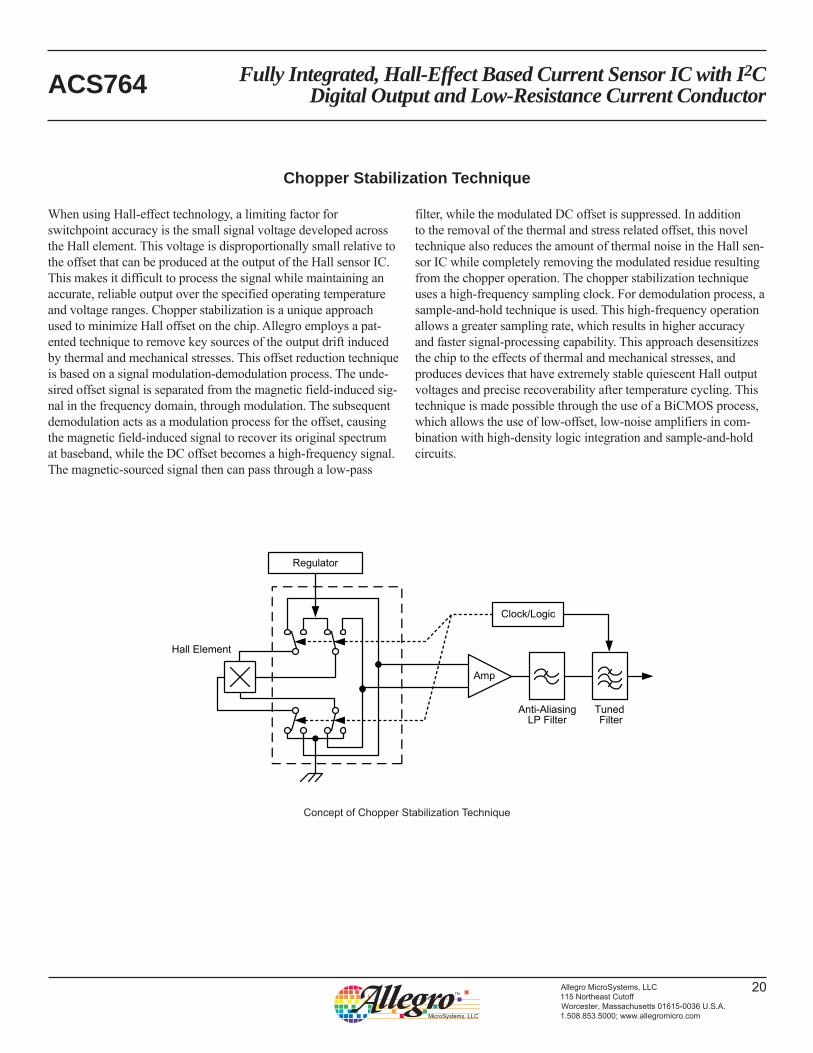
Concept of Chopper Stabilization Technique
Chopper Stabilization Technique
When using Hall-effect technology, a limiting factor for switchpoint accuracy is the small signal voltage developed across the Hall element. This voltage is disproportionally small relative to the offset that can be produced at the output of the Hall sensor IC. This makes it difficult to process the signal while maintaining an accurate, reliable output over the specified operating temperature and voltage ranges. Chopper stabilization is a unique approach used to minimize Hall offset on the chip. Allegro employs a pat-ented technique to remove key sources of the output drift induced by thermal and mechanical stresses. This offset reduction technique is based on a signal modulation-demodulation process. The unde-sired offset signal is separated from the magnetic field-induced sig-nal in the frequency domain, through modulation. The subsequent demodulation acts as a modulation process for the offset, causing the magnetic field-induced signal to recover its original spectrum at baseband, while the DC offset becomes a high-frequency signal. The magnetic-sourced signal then can pass through a low-pass
filter, while the modulated DC offset is suppressed. In addition to the removal of the thermal and stress related offset, this novel technique also reduces the amount of thermal noise in the Hall sen-sor IC while completely removing the modulated residue resulting from the chopper operation. The chopper stabilization technique uses a high-frequency sampling clock. For demodulation process, a sample-and-hold technique is used. This high-frequency operation allows a greater sampling rate, which results in higher accuracy and faster signal-processing capability. This approach desensitizes the chip to the effects of thermal and mechanical stresses, and produces devices that have extremely stable quiescent Hall output voltages and precise recoverability after temperature cycling. This technique is made possible through the use of a BiCMOS process, which allows the use of low-offset, low-noise amplifiers in com-bination with high-density logic integration and sample-and-hold circuits.

Fully Integrated, Hall-Effect Based Current Sensor IC with I2C Digital Output and Low-Resistance Current ConductorACS764
21Allegro MicroSystems, LLC115 Northeast CutoffWorcester, Massachusetts 01615-0036 U.S.A.1.508.853.5000; www.allegromicro.com
Package LF, 24-Pin QSOP
0.635 BSC
0.250.15
0.25 MAX
1.75 MAX
8º0º
1.270.41
0.25 BSC
1.04 REF
8.66 ±0.10
3.91 ±0.10
0.300.20
5.99 ±0.20
C0.2024X SEATING
PLANEC
0.635
2.30
5.00
0.40
21
24
GAUGE PLANESEATING PLANE
A
C
CB
A
For Reference Only, not for tooling use (reference JEDEC MO-137 AE) Dimensions in millimetersDimensions exclusive of mold flash, gate burrs, and dambar protrusions Exact case and lead configuration at supplier discretion within limits shown
B
Reference pad layout (reference IPC7351 SOP63P600X175-24M) All pads a minimum of 0.20 mm from all adjacent pads; adjust as necessary to meet application process requirements and PCB layout tolerances
Terminal #1 mark area
PCB Layout Reference View
Standard Branding Reference View
N = Device part number T = Temperature code LF = (Literal) Package type A = Amperage
TLF-AAA
LLLLLLLLLLL
NNNNNNNNNNNNN
Branded Face
Branding scale and appearance at supplier discretion

Fully Integrated, Hall-Effect Based Current Sensor IC with I2C Digital Output and Low-Resistance Current ConductorACS764
22Allegro MicroSystems, LLC115 Northeast CutoffWorcester, Massachusetts 01615-0036 U.S.A.1.508.853.5000; www.allegromicro.com
Copyright ©2010-2013, Allegro MicroSystems, LLC I2C™ is a trademark of Philips Semiconductors.
Allegro MicroSystems, LLC reserves the right to make, from time to time, such de par tures from the detail spec i fi ca tions as may be required to permit improvements in the per for mance, reliability, or manufacturability of its products. Before placing an order, the user is cautioned to verify that the information being relied upon is current.
Allegro’s products are not to be used in any devices or systems, including but not limited to life support devices or systems, in which a failure of Allegro’s product can reasonably be expected to cause bodily harm.
The in for ma tion in clud ed herein is believed to be ac cu rate and reliable. How ev er, Allegro MicroSystems, LLC assumes no re spon si bil i ty for its use; nor for any in fringe ment of patents or other rights of third parties which may result from its use.
For the latest version of this document, visit our website:www.allegromicro.com