active magnetic bearing driver circuit design featuring
TRANSCRIPT

ISRN UTH-INGUTB-EX-E-2015/12-SE
Examensarbete 15 hpDecember 2015
Active magnetic bearing driver circuit design featuring current measurement integration
Lukas Girlevicius

Teknisk- naturvetenskaplig fakultet UTH-enheten Besöksadress: Ångströmlaboratoriet Lägerhyddsvägen 1 Hus 4, Plan 0 Postadress: Box 536 751 21 Uppsala Telefon: 018 – 471 30 03 Telefax: 018 – 471 30 00 Hemsida: http://www.teknat.uu.se/student
Abstract
Active magnetic bearing driver circuit design featuringcurrent measurement integration
Lukas Girlevicius
Researchers at Uppsala University are developing a flywheel energy storage device intended to be used in electrical vehicles. Kinetic energy storage technology has potential to make purely electric powertrain both more effective and efficient. While deployment of the third prototype is approaching there has been a request for a more precise and noise-immune circuitry to power active magnetic bearings that hold and stabilise the rotor. A similar circuit designed for powering electromagnets was recently developed at the Uppsala University’s Electricity department and is used as a template in development of the new active magnetic bearing driver circuit. Current measurement integration technique is tested and implemented as a way to increase circuit’s control feedback loop performance. To further boost precision and noise-immunity 0-20 mA current loop signals are adapted as the standard for output signals. Results of this project include a thorough analysis of the electromagnet driver circuit development, implementation of a new current sensing technique including an experimental self-inductance measurement, printed circuit board layout design and a full list of components necessary to power and control two sets of active magnetic bearings consisting of 8 individual electromagnets.
ISRN UTH-INGUTB-EX-E-2015/12-SEExaminator: Nora MassziÄmnesgranskare: Johan AbrahamssonHandledare: Magnus Hedlund

Foreword This bachelor thesis work was done at the Uppsala University’s Department of Electricity. Special thanks to PhD Johan Abrahamsson for introducing me to the flywheel research group and making this thesis work possible. Warm thank you goes to this thesis supervisor, PhD candidate Magnus Hedlund, for all the inspiration and support I have received during period of this project. As a token of gratitude I hereby declare PhD candidate Tobias Kamf and MSc Fredrik Evestedt my personal heroes because of their help and contributions.
3

Table of Contents
Nomenclature 1. Introduction
1.1 Background 1.2 Objective 1.3 Restrictions
2. Theory 2.1 Flywheel energy storage 2.2 NI CompactRIO 2.3 Active magnetic bearings 2.4 Electromagnetic interference 2.5 Power electronics 2.6 Analog electronics 2.7 Digital electronics 2.8 Current loop measurement signal 2.9 Software
2.9.1 LTSpice IV 2.9.2 Mathworks Matlab and Simulink 2.9.3 NI Labview 2.9.4 CadSoft Eagle
3. Method 3.1 Electromagnet driver circuit development analysis 3.2 Adoption of electromagnet driver circuit subcircuits 3.2 Current integration measurement technique
3.2.1 Background 3.2.2 Simulation 3.2.3 Circuitry 3.2.4 Implementation 3.2.5 Axis position measurements using current integrators
3.3 Current loop measurement signal 3.4 AMB driver circuit PCB Layout
4

4. Results 4.1 Integrator Circuit performance 4.3 Current loop signal implementation 4.4 Printed circuit board design
5. Analysis and Discussion 5.1 Operational Specifications and requirements 5.2 PCB Design 5.3 Inputs and Outputs 5.4 Costs 5.5 Future work and improvements
6. Conclusion References Appendix
List of electronic components List of other parts PCB Map
5

Nomenclature FES Flywheel energy storage AMB Active magnetic bearings EMI Electromagnetic interference HBridge Power electronics circuit able of delivering current to the load bidirectionally Opamp Operational amplifier EMD Electromagnet driver circuit developed by Tobias Kampf PWM Pulse Width Modulation V Voltage [V] I Current [A] or Moment of inertia [kg*m^2] R Resistance [Ω] P Power [W] ω Angular velocity [rad/s]
6

1. Introduction
1.1 Background
Today flywheels are most commonly associated with the internal combustion engine, where it balances the engine’s operation by providing continuous rotational energy between piston’s strokes. The rotating mass of the flywheel offers a medium to efficiently store large amounts of energy for a shorter period of time. Using a high performance flywheel as a buffer between the electrochemical battery and the electric motor would extend the battery’s capacity and longevity. High rotation speeds that are necessary to achieve this performance can be sustained by placing the rotor in a vacuum chamber and supporting it with active magnetic bearings. These consist of several electromagnets surrounding the center axis at two locations. By constantly pulling with an equal force these magnets keep the rotating body suspended in the center while allowing it to revolve around it’s axis freely. To balance this system precise position of the body and force exerted by every electromagnet have to be known. Therefore a control feedback loop consisting of position and the current measurements are aiding a controller device to actively balance the body supported by the electromagnets. Accuracy of these measurements is very important to the overall performance of the magnetic bearings and the flywheel energy storage system as a whole. There is need of analog, digital and power electronics to operate active magnetic bearings and it makes for an interesting and challenging circuit to design. Flywheel energy storage devices are already being used in transportation, uninterrupted power supplies and aerospace applications. The flywheel research group at Uppsala University’s Electricity Department is working on improving the current flywheel technology in order to make it available for the broader market. This technology has several advantages such as high energy density, fast discharge rate and long lifetime while the complexity of a complete system is one of its disadvantages. A properly designed FES would be a great addition to large electrical vehicles such as trucks or busses, where frequent high power discharges that have a detrimental effect to the battery’s health could be handled by the flywheel.
7

1.2 Objective
Researchers at the division of electricity at the Uppsala University are soon deploying a new flywheel energy storage prototype and a new set of improved driver circuits to power the active magnetic bearings were requested. The new circuit has to consist of 8 full Hbridges capable of operating at maximum supply voltage of 100 V, maximum current of 10 A and switching speeds of up to 50 kHz. The current delivered to every individual electromagnet in the bearings has to be precisely measured and sent back to the controller by using a current loop signal. The circuitry needs to be robust and immune to electromagnetic interference as it will be working alongside high power components. Development of the new active magnetic bearing driver circuit should be based on a comparable and recently developed electromagnet driver circuit. The design of this circuit will be studied, analysed and summarised so that the new so that it is clear how the new driver is following and improving upon existing circuit design.
1.3 Restrictions
This project focuses on development and design of a new driver circuit. Performance of this circuit together with the rest of the flywheel circuitry is prioritized but not guaranteed as it may need additional hardware such as an interface card for optimal compatibility with the controller device.
8

2. Theory
2.1 Flywheel energy storage
The energy storage capacity of a typical flywheel used in combustion engines is usually very limited, as it rotates on mechanical bearings at relatively low speed of a few thousands revolutions per minute. However there are ways to make a flywheel perform on a level where it would be competing with batteries in terms of energy storage density and capacity. Energy stored in a rotating body is equal to the product of moment of inertia I and square of the angular velocity ω, divided by two:
.IωEk = 21 2
Geometry and mass of the rotating body determine moment of inertia but it is clear that because of the square proportionality a high rotation speed is the key factor in increasing flywheel energy storage capacity. Limiting factors such as aerodynamic drag and frictioncaused wear of bearings also depend on the rotation speed, reducing efficiency of the whole system. Therefore many modern FES devices are avoiding these negative effects by placing the rotating body in a vacuum chamber and keep it levitating by using magnetic bearings. An electrical reluctance motor is integrated into the device in order to allow efficient conversion between kinetic and electric forms of energy, broadening the list of FES’s potential applications (Abrahamsson 2011).
Figure 1. Flywheel energy storage device developed at Uppsala University (Abrahamsson 2011).
9

2.2 NI CompactRIO
National Instruments CompactRIO embedded realtime controller is at the core of the whole FES system developed by the Flywheel research team. Through a stack of various analog and digital swappable I/O modules CompactRIO is overseeing everything from power management to position sensors, including the active magnetic bearings control. Its processor and FPGA unit are programmable in Labview graphical environment. It’s adaptability has proven an asset during the years as it is easy to add additional circuitry and generate new control signals. Hence the CompactRIO is intended to deliver and receive all signals from the driver circuit developed in this project.
2.3 Active magnetic bearings
Most commonly implemented magnetic bearings use actively controlled electromagnets. A bias current is activating one or several pairs of opposing electromagnets placed around an axis. While the magnets are pulling the axis, a position sensor is keeping track of the axis and making adjustments in order to keep it balanced and centered. Therefore it is necessary to measure the current delivered to the electromagnets so that it can be accurately adjusted. This type of magnetic bearings offers several advantages such as variable dynamics and complete monitoring of the system performance (Abrahamsson 2011).
Figure 2. Pair of electromagnets in AMB operation (Abrahamsson 2011).
The third iteration of the flywheel energy storage prototype, just like the previous one, will feature two sets of radial active magnetic bearings consisting of two pairs of electromagnets each. This means that the current will have to be delivered, measured and controlled in 8 separate devices.
10

2.4 Electromagnetic interference
Electromagnetic interference is a high frequency energy that interferes with the operation of electronic devices. It can be produced externally or by the device itself. Coupling is an electrical relationship between two or more signals in which they are affecting each other. In case of EMI these relationships are highly undesirable as they adversely affect signal quality. There are four basic EMI coupling mechanisms :
Figure 3. Different types of EMI (Wikimedia)
Conductive coupling occurs when there is a direct conductive connection, such as wire or
metal enclosure, connecting the two systems. It is easily avoidable by proper isolation and separation of the conductors.
Inductive coupling is the unwanted magnetic induction of electrical current between two closely located conductors. It is particularly difficult to avoid at high currents and frequencies. The best solution is to place the susceptible conductors as far away as possible from highly inductive ones.
Capacitive coupling, also known as parasitic capacitance, is the electrical induction of voltage caused by an electric field between two conductors. It can be avoided by placing the conductors further apart and having a ground line in between them.
Radiative coupling occurs when a circuit acts as an antenna and picks up unwanted high frequency signals. It can be anything from radio or cellphone signals to sun storm or background radiation. This can be prevented by shielding certain components or the whole circuit with grounded conductive material.
(PCB Design guidelines for reduced EMI by Texas Instruments 1999).
11

2.5 Power electronics
Power electronics are electrical circuits intended to control the flow of electrical energy. These circuits are capable of handling power flows at much higher levels than regular small signal electronics. In the FES prototype and AMB in particular, power electronics are the link between the power supply, control devices and the load. Figure 4 illustrates this relationship in terms of a block diagram. In case of the AMB driver circuit the energy source would come from an external power supply, CompactRIO acts as a control circuit while electromagnets are the loads.
Figure 4. Block diagram of power electronics as part of a larger system (Rashid 2011).
The HBridge is one of the most commonly used power electronics circuits. It is the only piece of power electronics used in the AMB driver circuit, hence it will be referred to as Hbridge in this paper. Consisting of an arrangement of 4 power transistors in an H shaped formation, the load being connected between the lower and the upper bridge as shown in figure 5, Hbridge is capable of controlled and bidirectional power delivery. Pulse Width Modulated (PWM) control signal switches between diagonally placed transistors S1S4 and S2S3 in order to change direction of the current. Opening upper S1S3 or the lower S2S4 bridges cuts the power delivery but this feature will not be used in this the third prototype of FES (Rashid, 2011).
Figure 5. HBridge circuit (Wikimedia).
12

2.6 Analog electronics
Analog electronics work with low power signals that are continuous over time. Most of the natural phenomena such as electrical current are also continuous so they can only be measured by analog circuits. Since analog electronics operate in realtime it comes with a cost of some inherent noise and increased sensitivity to EMI (Analog Devices, 2015). While the transistor is one of the most basic analog component it is more practical to use operational amplifiers also know as opamps. These are made of tens to hundreds of transistors offering flexibility, high bandwidths and robust performance. Common mode rejection ratio (CMRR) is a measure of how well an opamp is rejecting the part of a signal that is common on both positive and negative inputs. Since that part is most often caused by EMI and is referred to as noise, CMRR is sometimes called noise rejection ratio. Because t rnoise rejection There are many various opamp circuits but the unity gain buffer, inverting amplifier, differential amplifier and opamp integrator are the ones that are being used in the design of the new AMB driver circuit.
Figure 6. Operational amplifier circuits (Wikimedia).
1. Unity gain buffer is a high input low output impedance circuit that replicates the input voltage at its output: It is used to assist circuits with low power signals or high output impedances.
.V in = V out 2. Inverting amplifier features a current loop feedback which makes it suitable for inverting,
amplifying and generating a current signal. .V in = − V out ∙
RfRin
13

3. Differential amplifier performs the mathematical operation of subtraction, amplifying only the difference between two inputs, which is useful for measurement of voltage drop.
.V V )V out = ( in 1 − in 2 4. Opamp integrator performs the mathematical operation of integration of the input
current. The integrated current stores charges on the input side of the capacitor causing an inverse voltage at the output.
(t) dtV out = − 1RC ∫
t1
t0V in .
(Molin, 2009).
2.7 Digital electronics
Digital electronics represent a signal in discrete levels, called logic levels, as opposed to the continuous spectrum of their analog counterparts. These devices are useful since it is easier to control equipment by switching between distinct states (most often on/off). For that reason digital signals are more immune to EMI. However the rapid switching nature of digital components create interference that can be harmful to analog signals. The FES is controlled by a digital automation controller CompactRIO that uses digital signals to interact with the AMB driver circuit. A digital gate driver receives the control signal and operates the Hbridge accordingly. Analog current measurements received by the CompactRIO are first converted to digital data and then processed by the controller. Several logic gates such as inverters, ANDgates and D flipflops are used in the AMB circuit to provide timing sequences and lower the amount of input signals.
Figure 7. CompactRIO realtime controller (National Instruments).
14

2.8 Current loop measurement signal
It was requested that the current measurement would be reported back to CompactRIO using a current loop signal. This means that measurement values will be represented by a small current that is proportionate to the current in the electromagnets. Current as a signal bearer is inherently more immune to noise because EMI induced current are tiny compared to the signal. Robustness of this signal is further increased by the closed loop feedback that adjusts voltage so that the current stays stable. 420 mA is a common signal range for industrial process control instruments. Zero current would indicate that the sensor/device is broken and has to be replaced, which is a useful feature in large factories containing thousands of sensors (Acromag Inc, 2015).
Figure 7. An example of a current loop signal transmission (National Instruments).
2.9 Software
An array of simulation and design software was used in order to examine, simulate and design the AMB circuit. A short summary of the programs used is provided in this subchapter.
2.9.1 LTSpice IV
LTSpice IV is a highperformance electrical circuit simulator capable of dealing with complex electrical circuits and visualising various signals. While not being able to simulate entire EMD or AMB circuits due to the lack of several IC models, this freeware was successfully used for smaller simulations and verifications. Generally it was the first step between a theoretical electrical circuit and its implementation.
15

2.9.2 Mathworks Matlab and Simulink
Matlab is a powerful computational software that can perform even the most complex simulations. Simulink is an additional module that offers readymade tools and algorithms to simulate electrical systems. Since everyone working or studying at Uppsala University can acquire a MATLAB license it is frequently used for any type of mathematical computations.
2.9.3 NI Labview
Labview is a graphical programming language that is used to program and control CompactRIO as well as its’ expansion modules in real time. Labview was used to generate signals similar to the ones that will be controlling the Hbridges and current measurement components.
2.9.4 CadSoft Eagle
Eagle is a simple to use printed circuit board (PCB) design software that is commonly used in various electronics projects at Uppsala University. Freeware version allows users to make 2layer PCBs of a limited size but since the Electricity Department holds a professional license there are no size restrictions and 16 signal layers are available. Division between the electric circuit schematic and the actual circuit board views enables design of a circuit theoretically first before the transition to PCB view where every component and wire has to be placed on the board manually.
16

3. Method
3.1 Electromagnet driver circuit development analysis
The project started with a study, analysis and documentation of the electromagnet driver circuit developed by PhD candidate Tobias Kamf at the Uppsala University’s Electricity Department. Since this circuit was designed to deliver current to a high impedance inductive load. Ratings for the system were as follows: voltage of 24V, maximum current of 5A and switching frequency of <100 kHz. These specifications are lower than the ones for the magnetic bearing driver circuit but there are many valuable lessons to be learned from this circuit. The first step was the creation of a detailed list comprising all ICs used in latest version of the EMD circuit. In order to break down the complexity of this system every component was analysed individually by studying the datasheets. The second step was analysing the circuit schematics in order to understand how these components interact and form a complete system. The final step was a study of the PCB layout: supply and ground plane design, IC package choice, component placement and other practical matters. Through all the steps designer of the EMD circuit was interviewed, explaining and motivating various design choices. The final circuit blueprints are shown in figure 8 and figure 9 below.
Figure 8. Schematic of the final version of the EMD circuit (Kamf).
17

Figure 9.PCB layout of the final version of the EMD circuit (Kamf).
The following paragraphs briefly describe development of the EMD circuit from the first to the final generations, such as the circuit shown in figure 10. This chronological analysis is useful when trying to understand the circuit “bottom up”. That approach is especially valuable when learning of the development process is just as important as the final solution.
1. A basic Hbridge circuit was built on a prototype board using nchannel power mosfet transistors that met the requirements. The transistors had to be arranged in a straight line since the standard Hformation made it hard to avoid control signals crossing the high current wires. In order to control the current it needs to be monitored. Real time current measurements are necessary to actively control the delivered to the load. This is done by placing a very low ohmic resistance anywhere in the Hbridge and then measuring the voltage drop. Two shunt resistors of 0,05 Omh each were placed on the ground end of the circuit. Generic instrumentation amplifiers used for current measurements and a HIP4080 Hbridge driver powering the gate signals were set up on a separate breadboard. Control was also done externally using a simple logic circuit. For testing purposes a
18

ferromagnetic core coil similar to an electromagnet was used as the load. The complete driver circuit showed satisfactory results and the printed circuit board design was started.
2. The new prototype circuit was based on a single twolayer printed circuit board, using
through hole mounted control and power electronics. In addition to previously described components, a charge pump was introduced to provide a negative rail voltage to the operational amplifiers. The circuit was still controlled by an external logic circuit, operating one side of the Hbridge at a time. During testing an unacceptable amount of noise was present in nearly all signals and the power transistors were producing too much excess heat. Since all the components were sharing a homogenous ground plane on the bottom layer of the circuit board, it was suspected that the rapid switching operation of power transistors interfered with the rest of components. A new pcb design had to be made to protect the more sensitive driver and current measurement electronics. Similar circuits were studied to find the most viable design solution.
3. This iteration introduced a lot of new design and component changes. Analysis of similar circuits showed that it is common practice to separate power component’s ground and voltage planes from rest of the circuit while still maintaining a common reference. It is done by creating an insulating divider between the conducting plane segments but not separating them entirely, similarly to a breakwater protecting a harbor. Fast switching and high power components usually are isolated by removing any conducting material on the back layer of the pcb to prevent induction of noise in other planes. This was especially applicable to the new surface mounted Texas Instruments mosfets CSD88537ND, chosen to replace the bulky and inefficient hole mounted transistors. These are completely encapsulated and lack a proper heatsink. Drain and source nodes were given a larger conducting surface layer than electrically necessary to improve heat dissipation and ensure optimal operational temperatures. Bulky shunt resistors from the lower bridge were replaced by a single low profile 0,025 Ohm shunt resistor directly on the load line. This design choice lowered the amount of components but the generic instrumental amplifier had to be replaced by a high CMRR dedicated shunt monitor to deal with the switching polarity of the measured current. This component requires a negative rail voltage so a charge pump was to be used. A fuse was introduced to protect the circuit components in case of power transistor failure. Testing showed mediocre performance with noise in both control and measurement signals. While the power electronics were isolated from rest of the circuit, the charge pump was unshielded and emitting too much high frequency noise. Isolating this component was impractical and therefore an external 15 V supply was adopted in the final versions.
19

Figure 10. One of the latest EMD circuit prototypes (Kamf).
20

3.2 Adoption of electromagnet driver circuit sub-circuits
It is important to note that while the whole circuit will be redesigned, certain subcircuits of the EMD circuit have all the desired functions and have been adopted straight into the AMB circuit. A schematic of the inherited circuitry is shown in figure 11. After that follows a list and description of theese.
Figure 11. Schematic of components inherited from the EMD circuit (Kamf).
HBridge circuit layout was designed for two dual Nchannel power MOSFETs. There are several SO8 packaged power transistors that are able to deliver power at ratings requested and well above. All Nchannel MOSFET HBridge is the most efficient alternative as it has the lowest onresistance. The only consideration is that the high side transistors require a gate signal that is at higher voltage than the drain voltage, which is the supply. However there are driver ICs developed particularly for this application that use a bootstrap capacitor to generate gate signal pulses required to switch the high side transistors on.
21

Power MOSFET full bridge driver Intersil HIP4081a is kept since it is tested to operate properly together with the previous transistors and its maximum ratings are deemed sufficient to meet the specification. IC’s logic threshold levels are compatible with both 5 and 15 V signals, allowing control straight from the NI9401 digital input/output module. HIP4081a will be sending out bootstrapped high power and high frequency pulses that are necessary to control the power MOSFETs. As a result of this, it will create a lot of EMI and special consideration will have to be taken in order to minimise its impact on the performance of other circuits.
Current measurement is done inside the Hbridge circuit by measuring voltage drop over
a small value shunt resistor connected in series with the load. This technique allows bipolar measurement but requires a differential amplifier with a high CMRR in order to measure the voltage drop. Analog Devices AD8210 is a suitable component for this task with 120 dB CMRR and therefore this current measurement solution will be adopted in the AMB driver circuit. AD8210 has gain of 20 times and its output voltage has a range of 0 to 5 V. Since the maximum current specification of the EMD circuit is 5 A it will be necessary to replace adjust the shunt resistor value in order to accommodate measurements up to 10 A. Figure 12 illustrates the current measurement circuit used in the EMD and AMB circuits.
Figure 12. Hbridge current measurement (Analog Devices).
22
3.2 Current integration measurement technique
3.2.1 Background
All of the EMD circuits featured instantaneous current measuring at discrete intervals. In this operation an A/D is converting the measurement signal into digital data that is fed back to the control device. The problem with this measurement technique, apart from the errors that come with discretisation, is that it offers low immunity to noise. A voltage spike caused by EMI will be recorded as a high value while the average signal value might be much lower. This can cause problems in the feedback loop as the current measurement together with axis position measurements determine the current that will be delivered to the electromagnet during the next control period. Noise introduced in this complex system lowers the maximum rotation speed of the flywheel as the active magnetic bearings are not able to deliver their best axisbalancing performance.
3.2.2 Simulation
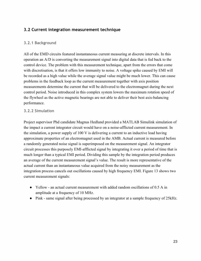
Project supervisor Phd candidate Magnus Hedlund provided a MATLAB Simulink simulation of the impact a current integrator circuit would have on a noiseafflicted current measurement. In the simulation, a power supply of 100 V is delivering a current to an inductive load having approximate properties of an electromagnet used in the AMB. Actual current is measured before a randomly generated noise signal is superimposed on the measurement signal. An integrator circuit processes this purposely EMIafflicted signal by integrating it over a period of time that is much longer than a typical EMI period. Dividing this sample by the integration period produces an average of the current measurement signal’s value. The result is more representative of the actual current than an instantaneous value acquired from the noisy measurement as the integration process cancels out oscillations caused by high frequency EMI. Figure 13 shows two current measurement signals:
Yellow an actual current measurement with added random oscillations of 0.5 A in amplitude at a frequency of 10 MHz.
Pink same signal after being processed by an integrator at a sample frequency of 25kHz.
23

Figure 13. Noisy signal before and after integration (Hedlund).
This simulation provided evidence that a current integration feature would be a beneficial addition to the magnetic bearing driver circuit as it greatly reduces the impact EMI has on the quality of the current measurements.
3.2.3 Circuitry
Since current integrator is a very basic Opamp circuit it first seemed like a simple task to develop a complete integration subcircuit. Sample & Hold functionality is critical since the integrator should stop integrating and hold its value while the CompactRIO module is reading the signal. After measurement acquisition is done the integrator should reset and start another integration period. A considerable amount of time was spent on this but it proved that a circuit with all the desired features such as reset and sample & hold would need quite a large arrangement of timers, logic gates and transistors working perfectly in sync. After some online research an integrated circuit capable of integration and all the other features was found. Texas Instruments ACF 2101 Dual Switched Integrator (Figure 11.) features two sets of Opamps integrating over 100pf precision capacitors and TTLlogic controlled hold, reset and select switches. Having a select feature enables two integrators to work in a complementary fashion, one integrates while the other holds a measurement value. If reset is done during the
24

holdperiod it possible to integrate over 100% of the measured signal. Since this IC presented a convenient and featurerich solution several were ordered for prototyping and testing.
Figure 14. ACF2101 function diagram and its 3 modes of operation (Texas Instruments).
3.2.4 Implementation
While the allinone current integration solution provided by the dual integrator IC fit perfectly in theory, it had to be adopted and tested together with rest of the driver circuit. Since the integrator circuit is dependant on several logic input signals triggering between Integrate, Hold and Reset modes of operation, it was most convenient and efficient to use the rising edge of the main PWMsignal for triggering. Integrate and Hold periods have to be controlled by a 5 V logic 50% duty cycle signal so that both periods are equal in length. Maximum frequency of the PWMsignal is 50 kHz which is halved in order to dedicate half of this period for integration and the other half for holding the measurement value. Integrator HOLD signal frequency of 25 kHz translates to 20 us of integration and another 20 us for holding which provides enough time for the CompactRio to read the measurement (7 us), reset (6 us) and settle at 0 V (2 us) before another integration period starts. A risingedge triggered D flip flop modulates the PWMsignal into a 25 kHz square
25

wave that works as the logical HOLD signal for the integrator A while the inverse of this signal controls integrator B. The RESET signal has to come approximately halfway through the HOLD period and since the operating frequencies of this whole system can vary, the easiest way is to send a RESET signal directly from one of the CompactRIO digital output modules. The SELECT signal is used to switch between the two integrators and since only the integrator in Hold mode is of interest, this signal can be dependant on HOLD. More precisely SELECT A is the inverted HOLD A signal. Figure 15 illustrates the logic circuit used to derive control signals for a single integrator pair.
Figure 15. Integrator control signal logic model.
Besides consideration of the necessary logic control signals it is also important to note that ACF2101 maximum input current is of 100 uA which integrates negatively from 0 to 10 V on the output pin. By using the formula in figure 13 it is possible to calculate the input current that is suitable for any combination of integration capacitor and operating frequency.
Figure 13. Integrator output voltage formula (Texas Instruments).
The PWMsignal at 50 kHz results in an integration period of 20 us. The builtin capacitor of 100 pF is used and 10 V is the maximum output voltage. Calculation of input current that yields maximum output under an integration period:
I (10 V 100 pF ) / ( 20 us) 50 uA . = * =
26

Shunt monitor AD8210 output range is 05 V with 5 V for a current of 10 A and 0 V for 10 A. Maximum output of 5 V should result in a 50 uA input current to ACF2101. This is achieved by connecting a 100 kΩ resistor in series with input. Resulting resolution of the current integrator is:
Measurement range / Actual current range) V / 20 A , 5 V /A. ( = 5 = 0 2
Figure 16. Testing integrator circuit with control signals from CompactRIO.
3.2.5 Axis position measurements using current integrators
Additional current integrators are considered to be added to the circuit in order to fully monitor the currents in the electromagnets. Even though implementing a dual integrator in complementary operation (described in the previous chapter) will read current values continuously, it will provide a sum of these values as a result. Dividing this value by the integration period time will yield an average value that is optimal for the feedback loop. Another important piece of information can be acquired through multiple simultaneous measurements, namely the current rate of change with respect to time.
27

Since selfinductance in an ACpowered coil (such as an electromagnet) is directly proportional to this change,
,(t) v = − L dtdi
it would be possible to use integrator measurements to determine and thus the selfinductancedt
di of the electromagnet in an active magnetic bearing. In turn, this relationship is directly proportional to the distance between the rotor axis and the electromagnet due to the fact that magnetic flux changes because of the changing reluctance caused by variations in the air gap. Measuring this distance for every electromagnet in an AMB would allow calculation of the rotor position, thus removing the need of additional position sensors connected to the feedback loop. This would make a single AMB driver circuit capable of both powering the bearings and conducting all the necessary control feedback measurements. The integrator IC is yet untested and its main objective remains to measure the average current. However in order to test the position measurement capabilities of this circuit an additional ACF2101 is connected to every Hbridge current sensor. Results of these measurements are delivered through a different output so that it does not occupy output pins and interfere with the main current measurements. Having this experimental feature turned off will have no effect for the rest of the AMB driver circuit performance.
28

3.3 Current loop measurement signal
There are several IC solutions such as Texas Instruments XTRseries that convert a voltage signal into an either 020 mA or 420 mA current loop signal. Due to their low cost several XTR117 ICs were purchased and tested with on a prototype board together with a signal generator and oscilloscope. However a problem with these ICs were that it has a builtin +5 V linear regulator that should power all of the input (measurement) circuitry and then all the current drawn has to return back to the IC through a local ground point. The integrator circuit is powered by both +5 V and 10 V supply which makes it impossible to mate it with this particular series of voltagetocurrent loop converters. Designing a current loop circuit using Opamplifiers was the option chosen. This provided more flexibility as the circuit could be designed to match the specific measurement components rather than adapting the measurement system to fit with the XTRseries. LTSpice was a great asset while testing various Opamplifier circuits that could properly condition the voltage signal.
Figure 17. Switched output with an opamp based voltagetocurrent converter.
Having 4 mA represent the minimum value of a measurement while 0 mA is an indication that the sensor malfunctioned is part of the industrial process standard but it is not necessarily the best option for the FES. Industrial instrumentation, especially sensors, are usually powered by the current loop signal itself these 4 mA are enough to keep the circuit running. However in case of the AMB driver no instruments are powered this way and there was no request for a current sensor failure detection feature. Hence it was deemed that the range of 04 mA can be added to the measurement signal range instead, resulting in a higher resolution 020 mA current loop signal. This is illustrated in the schematic and graph in figure 17 above.
29

3.4 AMB driver circuit PCB Layout
Digital and power electronics draw current in short, rapid surges that can disturb the power supply and ground potentials. Analog components on the other hand rely on these potentials to be stable in order to provide accurate performance. Hence it is critical to plan the layout of a mixed signal circuit in a way that is minimizing the possibility for interference. It is commonly recommended to use a completely separate circuit for analog components so that they don’t have to share ground or supply with switching digital and power electronics. As previously learned from the electromagnet driver circuit analysis however it is quite possible to use mixed signal components on the same circuit board. There are several features that should be incorporated in design of such circuit but the most important of these features is one of the most basic: to keep noisy components away and if possible shielded from the sensitive ones. Layout of this PCB follows design of the latest EMD circuit while making necessary adjustments to accommodate the increased number of components and signals. Since the complete AMB driver circuit has to power 8 bearings it needs 8 Hbridges along with all the current measurement components. Placing everything on a large single PCB would save components and enable use of the same HOLD, SELECT and RESET signals for every current integrator circuit. However due to the size of the resulting circuit board, it would take weeks to manually configure the layout. Hence 4 identical PCBs consisting of 2 Hbridges each will be produced and interconnected for more efficient use of the current integrator control signals. Several of the components will require special attention due to the fact that the AMB driver circuit is a mixed signal circuit. There are PCB placement guidelines provided in the datasheet of almost every IC used and these will be followed to ensure proper operational environment. Just like in the EMD circuit, large ground and voltage supply planes will cover every empty piece of the circuit board, increasing stability of their potential and improving thermal conductance (cooling). Decoupling capacitors will be placed next to the supply pin of every component in order to filter high frequency electromagnetic noise. Current measurement signal traces will be kept as short as possible in order to minimise risk of signal distortion by interference. After the current measurement signal has been integrated it will be converted to a current loop signal that can withstand nearby presence of noisy digital signals which will ease the component and trace placement.
30

4. Results
4.1 Integrator Circuit performance
A complete current measurement integrator circuit was assembled on a prototyping breadboard and tested together with control signals generated by the CompactRIO NI9401 module. A 10 kHz PWMsignal was chosen because while the ACF2101 should not have problems operating at the maximum frequency of 50 kHz, parasitic capacitances in the breadboard and measuring equipment used would distort the test results. An integration period of 100 us with a constant input current of 10 uA yielded a linear decline of the output voltage from 0 to 10 V. The capacitor discharge (reset) time was measured to 5 us and the capacitor voltage settling time was approximately 2 us, holding the values specified by the circuit’s producer Texas Instruments. Figure 18 shows the Hold A signal in yellow next to integrator A ouput in purple and inverted integrator B output in green color.
Figure 18. Complementary operation Figure 19. Multiplexed output signal The actual output signal of the integrator is multiplexed by the Select switching signal and is shown above in figure 19. The output node had to be grounded through a 50 kOhm resistor in order for the switch to operate. This will have negligible effect since output is connected to a unity gain buffer that stabilises the output signal. Because it is yet unclear how well the integrator circuit is going to perform in the AMB feedback control loop an additional current measurement method was introduced as a backup. It features a more conventional approach of using AD8210 output signal directly and only conditioning it by the VI converter in order to produce a current loop signal. Combination of a jumper and a cable socket change is necessary to switch between the two current measurement techniques.
31

4.3 Current loop signal implementation
Opamp inverting amplifier circuit can be used as a VI converter. The resulting current signal passes through the negative feedback resistor. Having this resistor at the receiver (one of the CompactRIO input modules) creates a closed current loop signal since the input is not sinking the signal current. Instead it measures the voltage drop over the feedback resistor with a differential amplifier. Texas Instruments OPA2132 high speed FET input opamp was chosen because it offers good performance in terms of high slew rate of 20V/us, wide bandwidth of 8 MHz, low noise of 8 nV / kHz and operates in the required +15 V region. High slew rate is important as the input signal will drop to zero when coming to the end of a hold period due to the capacitor being discharged (reset period) and then immediately rise when the integrator output is switched at the beginning of a new hold period. It is critical that the opamps adjust their voltage levels fast enough before CompactRIO starts reading the measurement signal. 20 V/us rating implies that a change from 0 to 10 V will be adjusted to in 0.5 us which is sufficiently fast compared to the 8 us total measurement signal reading period. Final resolution of the current measurement signal is 1mA per 1 A in the electromagnet.
Figure 20. Integrator and voltagetocurrent converter circuit schematic.
32

4.4 Printed circuit board design
The PCB circuit was designed using Cadsoft Eagle Professional software. Components for every subcircuit as well as miscellaneous parts such as wiretoboard connectors were chosen and are ready to be ordered. The circuits physical dimensions were kept minimal with consideration to the cost and space that it will occupy since 4 such PCBs will be used. 150 x 160 mm was the minimum size feasible by using only two signal layers. Signal traces of 0.4 mm width and isolation of 0.2 mm were used with all signals and planes except for the Hbridge part of the PCB. There the isolation between planes was increased to 1 mm and large planes were used as conductors for reduced resistive losses and better cooling. Both Hbridges are located on the left side of the circuit and are designed to be powered by a separate high power supply. This supply signal is given a large plane on the top layer with two 100 uF electrolytic capacitors placed next to every MOSFET pair to stabilise the voltage. As in the EMD circuit, Hbridges are connected to a ground plane that is separated from the rest of the components except for a little path next to the power supply connector. This little connection ensures that both ground planes have the same electric potential but prevents the EMI created by Hbridge to spread across the whole circuit. Since the shunt resistor is inside the Hbridge circuit differential amplifier AD8210 has to be placed next to it. The rest of the analog components such as integrators and other opamps were clustered right behind AD8210. Surrounded by the mosfet gate driver signal traces, this analog “island” is where all the sensitive signals are handled. Every component has its own supply voltage plain decoupled by at least one capacitor, most commonly a 100 nF ceramic. Negative 15 V power supply received a plane on the bottom side in order to reach the necessary opamp components. Digital components were placed right next to the left side DSub inputs because the PWMsignal together with main RESET will to go through a series of gates before being used to control the integrator circuits. Illustrated in the figure 21 is the complete CAD blueprint of the circuit, with top layer components, traces and conducting planes displayed in red and the bottom ones in blue. No components were placed on the bottom layer to keep the surface tidy and low profile.
33
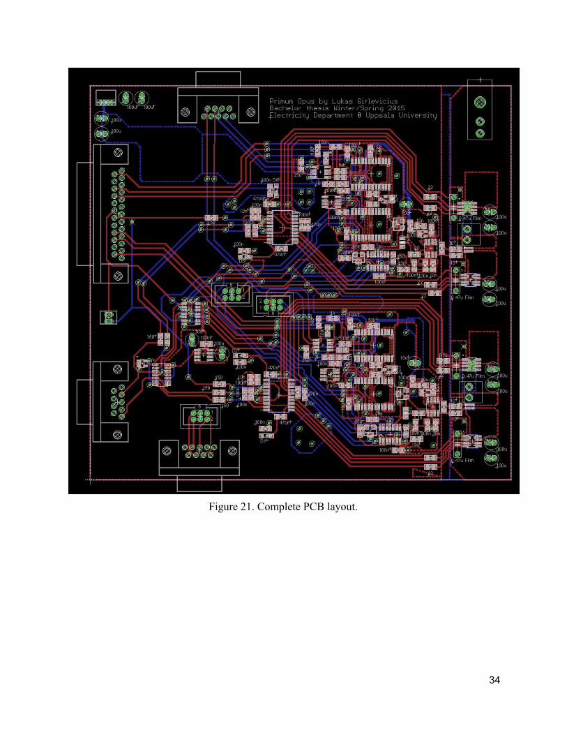
Figure 21. Complete PCB layout.
34

5. Analysis and Discussion
5.1 Operational Specifications and requirements
This AMB driver circuit has the following electrical specifications:
Nominal Maximum Requested
Small signal electronics power supply voltage + 15 V + 20 V Unspecified
Power electronics power supply voltage 60 V 60 V 100 V
Power electronics current output 10 A 15 A 10 A
PWMcontrol signal frequency 50 kHz 50 kHz 50 kHz
Since the dual power mosfet CSD88537ND and its driver were adopted from the EMD circuit the requested specification of 100 V supply for the Hbridge was not met. However the 50% higher maximum current rating of 15 A is able to deliver approximately the same amount of active power to the magnetic bearings with a supply voltage of 60 V. This however would lead to higher resistive losses since they are proportional to the square of the current. It is yet to be seen how this will affect the AMB performance as a power supply rated at 48 V was used in the previous FES prototypes (Abrahamsson 2011).
(requested) I 00V 0A 1 kV AS = V = 1 * 1 = (actual) 0V 5A 0.9 kV AS = 6 * 1 = Operating temperature range of 40 to +125 Celsius makes the circuit suited for outdoor or vehicular use if an appropriate watertight case is provided. The requirement of robust performance and noise immunity for the AMB driver circuit is somewhat relative to the previous circuits and should be tested once the circuit is assembled. Although it would be fair to assume that following design of previous iterations and adding additional noisereduction features should provide measurable improvements.
35

5.2 PCB Design
As a result of the design choices mentioned in chapter part 4.3 the complete PCB is distinctly divided in areas of digital, analog and power electronics. This makes it easy to overview and troubleshoot the circuit while also the risk of EMI between these components is minimised. Due to the large number of different signals at certain parts of the PCB, sometimes there was hardly enough space for signal traces either on the top or bottom layers. Increasing board size would have solved this problem but the circuit’s compact dimensions will be beneficial in terms of space occupied and material needed if a shielding case is added. Making a 4layer card instead could have been another solution but there was simply not enough time to redraw and rethink the circuit.
5.3 Inputs and Outputs
Total inputs (TTL or CMOS) Total outputs (020 mA)
8 PWMcontrol signal 8 Integrated current measurements
1 Enable 8 Current rate of change measurements
1 Reset
24 Current rate of change measurement
The circuit is compatible with both 5 V TTL and 15 V CMOS control signals. Enable and Reset signals are shared between the 4 circuit boards. Current rate of change measurements demand a large amount of input signals but those are not necessary for the intended AMB driver circuit operation.
5.4 Costs
Eurocircuits are chosen to manufacture the PCBs because of their userfriendly online order placement, fast delivery and competitive pricing. Order of 6 PCBs including a soldering stencil with a delivery of 5 working days was priced at approximately 270 Euro. Soldering stencil will ease soldering with a reflow oven that is available at one of the Electricity Department’s laboratories.
36

Components for the whole AMB driver circuit are purchased at Farnell due to the high availability of components and fast delivery. Approximated prices of all components is 400 Euro.
5.5 Future work and improvements
Since design of the AMB driver circuit built heavily upon the EMD circuit, certain limitations were inherited. Power MOSFETs in the Hbridge can be changed to higher rated ones, such as Vishay Siliconix rated at 100 V/ 35 A and having the same casing, but then it would also be necessary to swap the HIP4081a driver IC as well. Replacing the AD8210 with a shunt monitor IC of higher output range would provide better first current measurement stage resolution than 0.25 V / A. Increasing the amount of layers to 4 or 6 would probably lead to better EMI immunity and more optimal trace placement. This would leave almost none of the EMD design left but in order to achieve best performance it is often necessary to create new designs from scratch. A lot of future work can be done experimenting with position measurement through measurement of the current rate of change. If successful this solution could be beneficial in applications where position sensor placement is not practical.
6. Conclusion Design of a low profile, low noise and EMI immune AMB driver circuit capable of delivering high power at high frequencies is a challenging task due to the radically different EMI nature of components that have to be used. If precise current measurement are of key importance, separate circuit boards should be used for Hbridges and analog electronics. In some environments however it is impossible to avoid high frequency EMI and it is then better to use a circuit that is designed to operate in such conditions.
37

References
Abrahamsson, J. (2011). Kinetic energy storage and magnetic bearings, for vehicular applications. Uppsala: Department of Technological Sciences, Uppsala universitet.
Rashid, M.H. (2011). Power Electronics Handbook : Devices, Circuits and Applications, 3rd ed. uppl. Upper Saddle River, N.J. ; London: Pearson Prentice Hall. PCB Design Guidelines for Reduced EMI by Texas Instruments (1999) http://www.ti.com/lit/an/szza009/szza009.pdf Eurocircuits Design Guidelines by Eurocircuits (2015) http://www.eurocircuits.com/clientmedia/ecImage/pages/pcblayoutdata/ecdesignguidelines.pdf EMI, RFI, and Shielding concepts by Analog Devices (2009) http://www.analog.com/media/en/trainingseminars/tutorials/MT095.pdf
Introduction to Two Wire Transmitters by Acromag (2015)http://www.acromag.com/sites/default/files/Acromag_Intro_TwoWire_Transmitters_4_20mA_Current_Loop_904A.pdf High Speed Layout Guidelines by Texas Instruments (2006) http://www.ti.com/lit/an/scaa082/scaa082.pdf
80V/2.5A Peak, High Frequency Full Bridge FET Driver by Intersil (2004) https://www.intersil.com/content/dam/Intersil/documents/hip4/hip4081a.pdf All about EMI filters by Mel Berman (2008) http://www.digikey.com/Web%20Export/Supplier%20Content/Lambda_285/PDF/TDKLambda_all_about_emi_epmag.pdf?redirected=1
38

Appendix
List of electronic components
Component description Product name Units per PCB Farnell order #
Full bridge driver Intersil HIP4081 2 1561934
Dual power MOSFET TI CSD88537 4 2430179
Dual FETInput OpAmp TI OPA2132 2 1206934
Quad FETInput OpAmp TI OPA4132 2 1212302
5V Linear Regulator TI LM78L05ACM 3 9489436
Switched Dual Integrator TI ACF2101BU 4 1754679
Current sense amplifier AD8210YRZ 2 1274226
Current sense resistor PRL1632R012 2 2112882
Voltage Reference ADR361AUJZ 2 1117861
Hex inverter TI SN74AC04D 1 9590218
Dtype flip flop TI SN74LVC 1 1601171
Quad AND gate TI 74LV08 1 1085354
Schottky diode Avago HSMS2800 4 1056832
Potentiometer 500k Bourns 3214W1102E 2 988327
Potentiometer 1k Bourns 3214W1504E 2 988248
Small signal diode Multicomp 1N4148WS 4 1466524
Electrolytic capacitor 100u Panasonic EEUFM101 16 1219466
Film capacitor 0.47u Epcos B32653A 4 9751343
SMD Resistors and capacitors Various values 50+
39

List of other parts
Part description Units per PCB Farnell order #
Hbridge output terminal 2 9492003
Hbridge output wire housing 2 630470
Hbridge output crimp contact 4 630500
PCB coupling wire header 1 9491902
PCB coupling wire housing 1 3616186
PCB coupling wire crimp contact 2 617210
High voltage supply header 1 2383192
High voltage supply housing 1 2383175
High voltage supply crimp contact 2 2383188
Low voltage supply header 1 9491830
Low voltage supply housing 1 3357569
Low voltage crimp contact 8 3357533
Dsub headers 9/25 pins 3/1
Dsub housings and cables
40

PCB Map
This map is meant to provide guidance to the person assembling the circuit.
41

PCB coupling contact is used to share the global Reset and Enable signals between the paired circuit boards so that fewer DSub 25 connectors and cables are needed. Rest of the signals on the 25pin connector are purely for the experimental rotor position measurement. XOUT 1,2 are the output signals that these optional measurements provide. PWM 1,2 are the signals that control the Hbridge circuits and from which the integrator hold signals are derived. Current measurement output can be chosen to be either the regular direct voltage or the current integration measurement. However both of these are delivered through 2wire current signal. Schematic and PCB layout files can be accessed by the following link: https://www.dropbox.com/sh/fupuik8hwc52lmu/AADKMeKFonnreYWGPHmDBI44a?dl=0
42