adc0804-n - analog, embedded processing, … · translate this pageadc0804-n - analog, embedded...
TRANSCRIPT

Product
Folder
Sample &Buy
Technical
Documents
Tools &
Software
Support &Community
ADC0801, ADC0802, ADC0803, ADC0804, ADC0805SNOSBI1C –NOVEMBER 2009–REVISED JUNE 2015
ADC080x 8-Bit, µP-Compatible, Analog-to-Digital Converters1 Features 3 Description
The ADC0801, ADC0802, ADC0803, ADC0804, and1• Compatible With 8080-µP Derivatives – No
ADC0805 devices are CMOS 8-bit successiveInterfacing Logic Needed – Access Time 135 nsapproximation converters (ADC) that use a differential
• Easy Interface to All Microprocessors, or Operates potentiometric ladder — similar to the 256R products.as a Stand-Alone Deivce These converters are designed to allow operation
with the NSC800 and INS8080A derivative control• Differential Analog Voltage Inputsbus with Tri-state output latches directly driving the• Logic Inputs and Outputs Meet Both MOS anddata bus. These ADCs appear like memory locationsTTL Voltage-Level Specifications or I/O ports to the microprocessor and no interfacing
• Works With 2.5-V (LM336) Voltage Reference logic is needed.• On-Chip Clock Generator Differential analog voltage inputs allow increasing the• 0-V to 5-V Analog Input Voltage Range With common-mode rejection and offsetting the analog
Single 5-V Supply zero input voltage value. In addition, the voltagereference input can be adjusted to allow encoding• No Zero Adjust Requiredany smaller analog voltage span to the full 8 bits of• 0.3-Inch Standard Width 20-Pin DIP Package resolution.
• 20-Pin Molded Chip Carrier or Small OutlinePackage Device Information(1)
• Operates Ratiometrically or With 5 VDC, 2.5 VDC, PART NUMBER PACKAGE BODY SIZE (NOM)or Analog Span Adjusted Voltage Reference ADC0801, PDIP (20) 26.073 mm × 6.604 mmADC0803• Key Specifications
PDIP (20) 26.073 mm × 6.604 mmADC0802,– Resolution: 8 BitsADC0804 SOIC (20) 12.80 mm × 7.50 mm– Total Error: ±1/4 LSB, ±1/2 LSB and ±1 LSB(1) For all available packages, see the orderable addendum at– Conversion Time: 100 µs the end of the data sheet.
2 Applications• Operates With Any 8-Bit µP Processors or as a
Stand-Alone Device• Interface to Temp Sensors, Voltage Sources, and
Transducers
Typical Application Schematic ADC0801 Specified With ±¼ LSB Accuracy
1
An IMPORTANT NOTICE at the end of this data sheet addresses availability, warranty, changes, use in safety-critical applications,intellectual property matters and other important disclaimers. PRODUCTION DATA.

ADC0801, ADC0802, ADC0803, ADC0804, ADC0805SNOSBI1C –NOVEMBER 2009–REVISED JUNE 2015 www.ti.com
Table of Contents8.2 Functional Block Diagram ....................................... 121 Features .................................................................. 18.3 Feature Description................................................. 122 Applications ........................................................... 18.4 Device Functional Modes........................................ 143 Description ............................................................. 1
9 Application and Implementation ........................ 154 Revision History..................................................... 29.1 Application Information............................................ 155 Pin Configuration and Functions ......................... 39.2 Typical Applications ................................................ 226 Specifications......................................................... 49.3 System Examples ................................................... 406.1 Absolute Maximum Ratings ...................................... 4
10 Power Supply Recommendations ..................... 486.2 ESD Ratings.............................................................. 411 Layout................................................................... 486.3 Recommended Operating Conditions....................... 4
11.1 Layout Guidelines ................................................. 486.4 Thermal Information .................................................. 412 Device and Documentation Support ................. 496.5 Operating Ratings ..................................................... 5
12.1 Related Links ........................................................ 496.6 Electrical Characteristics........................................... 512.2 Community Resources.......................................... 496.7 AC Electrical Characteristics..................................... 512.3 Trademarks ........................................................... 496.8 Typical Characteristics .............................................. 812.4 Electrostatic Discharge Caution............................ 497 Parameter Measurement Information ................ 1012.5 Glossary ................................................................ 497.1 Tri-State Test Circuits and Waveforms................... 10
13 Mechanical, Packaging, and Orderable8 Detailed Description ............................................ 11Information ........................................................... 498.1 Overview ................................................................. 11
4 Revision History
Changes from Revision B (Feburary 2013) to Revision C Page
• Added Pin Configuration and Functions section, ESD Ratings table, Feature Description section, Device FunctionalModes, Application and Implementation section, Power Supply Recommendations section, Layout section, Deviceand Documentation Support section, and Mechanical, Packaging, and Orderable Information section .............................. 1
• Removed Ordering Information table .................................................................................................................................... 4
2 Submit Documentation Feedback Copyright © 2009–2015, Texas Instruments Incorporated
Product Folder Links: ADC0801 ADC0802 ADC0803 ADC0804 ADC0805

ADC0801, ADC0802, ADC0803, ADC0804, ADC0805www.ti.com SNOSBI1C –NOVEMBER 2009–REVISED JUNE 2015
5 Pin Configuration and Functions
NFH and DW Package20-Pin PDIP and SOIC
Top View
Pin FunctionsPIN
I/O DESCRIPTIONNO. NAME
1 CS I Chip Select2 RD I Read3 WR I Write4 CLK IN I External Clock input or use internal clock gen with external RC elements5 INTR O Interrupt request6 VIN(+) I Differential analog input+7 VIN(–) I Differential analog input–8 A GND I Analog ground pin9 VREF/2 I Reference voltage input for adjustment to correct full scale reading10 D GND I Digital ground pin11 DB7 O Data bit 712 DB6 O Data bit 613 DB5 O Data bit 514 DB4 O Data bit 415 DB3 O Data bit 316 DB2 O Data bit 217 DB1 O Data bit 118 DB0 (LSB) O Data bit 019 CLK R I RC timing resistor input pin for internal clock gen20 VCC (or VREF) I +5V supply voltage, also upper reference input to the ladder
Copyright © 2009–2015, Texas Instruments Incorporated Submit Documentation Feedback 3
Product Folder Links: ADC0801 ADC0802 ADC0803 ADC0804 ADC0805

ADC0801, ADC0802, ADC0803, ADC0804, ADC0805SNOSBI1C –NOVEMBER 2009–REVISED JUNE 2015 www.ti.com
6 Specifications
6.1 Absolute Maximum Ratingsover operating free-air temperature range (unless otherwise noted) (1) (2)
MIN MAX UNITSupply voltage (VCC) (3) 6.5 V
Logic control inputs –0.3 18Voltage V
At other input and outputs –0.3 (VCC +0.3)Dual-In-Line Package (plastic 260
Lead Temperature Dual-In-Line Package (ceramic) 300(Soldering, 10
Surface Mount Package Vapor Phase (60 seconds) 215 °Cseconds)Infrared (15 seconds) 220
Storage Temperature –65 150Package Dissipation at TA = 25°C 875 mW
(1) Stresses beyond those listed under Absolute Maximum Ratings may cause permanent damage to the device. These are stress ratingsonly, which do not imply functional operation of the device at these or any other conditions beyond those indicated under RecommendedOperating Conditions. Exposure to absolute-maximum-rated conditions for extended periods may affect device reliability.
(2) If Military/Aerospace specified devices are required, contact the Sales Office/Distributors for availability and specifications.(3) A Zener diode exists, internally, from VCC to GND and has a typical breakdown voltage of 7 VDC.
6.2 ESD RatingsVALUE UNIT
V(ESD) Electrostatic discharge Human body model (HBM), per ANSI/ESDA/JEDEC JS-001 (1) ±800 V
(1) JEDEC document JEP155 states that 500-V HBM allows safe manufacturing with a standard ESD control process.
6.3 Recommended Operating Conditionsover operating free-air temperature range (unless otherwise noted)
MIN NOM MAX UNITVCC 4.5 5 5.5 VAnalog Input Voltage GND – 0.05 VCC + 0.05 VDC
6.4 Thermal InformationADC080x ADC0802,
ADC0804THERMAL METRIC (1) UNITNFH (PDIP) DW (SOIC)
20 PINS 20 PINSRθJA Junction-to-ambient thermal resistance 38.5 63.8 °C/WRθJC(top) Junction-to-case (top) thermal resistance 23.4 27.2 °C/WRθJB Junction-to-board thermal resistance 19.5 31.8 °C/WψJT Junction-to-top characterization parameter 8.7 5.7 °C/WψJB Junction-to-board characterization parameter 19.4 31.3 °C/WRθJC(bot) Junction-to-case (bottom) thermal resistance — — °C/W
(1) For more information about traditional and new thermal metrics, see the Semiconductor and IC Package Thermal Metrics applicationreport, SPRA953.
4 Submit Documentation Feedback Copyright © 2009–2015, Texas Instruments Incorporated
Product Folder Links: ADC0801 ADC0802 ADC0803 ADC0804 ADC0805

ADC0801, ADC0802, ADC0803, ADC0804, ADC0805www.ti.com SNOSBI1C –NOVEMBER 2009–REVISED JUNE 2015
6.5 Operating Ratingsover operating free-air temperature range (unless otherwise noted) (1) (2).
MIN MAX UNITADC0804LCJ –40 85ADC0801/02/03/05LCN –40 85
Temperature °CADC0804LCN 0 70ADC0802/04LCWM 0 70
Range of VCC 4.5 6.3 VDC
(1) Absolute Maximum Ratings indicate limits beyond which damage to the device may occur. DC and AC electrical specifications do notapply when operating the device beyond its specified operating conditions.
(2) All voltages are measured with respect to GND, unless otherwise specified. The separate A GND point should always be wired to the DGND.
6.6 Electrical CharacteristicsThe following specifications apply for VCC = 5 VDC, TMIN ≤ TA ≤ TMAX and fCLK = 640 kHz (unless otherwise specified).
PARAMETER TEST CONDITIONS MIN TYP MAX UNITADC0801: Total Adjusted Error (1) With Full-Scale Adj. (See Full-Scale) ±1/4ADC0802: Total Unadjusted VREF/2=2.500 VDC ±1/2Error (1)
ADC0803: Total Adjusted Error (1) With Full-Scale Adj. (See Full-Scale) ±1/2 LSBADC0804: Total Unadjusted Error VREF/2=2.500 VDC ±1(1)
ADC0805: Total Unadjusted Error VREF/2-No Connection ±1(1)
ADC0801/02/03/05 2.5 8VREF/2 Input Resistance (Pin 9) kΩ
ADC0804 (2) 0.75 1.1Analog Input Voltage Range V(+) or V(–) (3) GND–0.05 VCC+0.05 VDC
DC Common-Mode Error Over Analog Input Voltage Range ±1/16 ±1/8 LSBVCC=5 VDC ±10% Over Allowed VIN(+) and VIN(–)Power Supply Sensitivity ±1/16 ±1/8 LSBVoltage Range (3)
(1) None of these ADCs requires a zero adjust (see Zero Error). To obtain zero code at other analog input voltages see Errors andReference Voltage Adjustments.
(2) The VREF/2 pin is the center point of a two-resistor divider connected from VCC to ground. In all versions of the ADC0801, ADC0802,ADC0803, and ADC0805, and in the ADC0804LCJ, each resistor is typically 16 kΩ. In all versions of the ADC0804 except theADC0804LCJ, each resistor is typically 2.2 kΩ.
(3) For VIN(−)≥ VIN(+) the digital output code will be 0000 0000. Two on-chip diodes are tied to each analog input (see block diagram)which will forward conduct for analog input voltages one diode drop below ground or one diode drop greater than the VCC supply. Becareful, during testing at low VCC levels (4.5V), as high level analog inputs (5V) can cause this input diode to conduct–especially atelevated temperatures, and cause errors for analog inputs near full-scale. The spec allows 50 mV forward bias of either diode. Thismeans that as long as the analog VIN does not exceed the supply voltage by more than 50 mV, the output code will be correct. Toachieve an absolute 0 VDC to 5 VDC input voltage range will therefore require a minimum supply voltage of 4.950 VDC over temperaturevariations, initial tolerance and loading.
6.7 AC Electrical CharacteristicsThe following specifications apply for VCC=5 VDC and TMIN≤ TA≤TMAX (unless otherwise specified)
PARAMETER TEST CONDITIONS MIN TYP MAX UNITfCLK = 640 kHz (1) 103 114 µs
TC Conversion TimeSee (2) (1) 66 73 1/fCLK
Clock Frequency 100 640 1460 kHzfCLK VCC = 5V (2)
Clock Duty Cycle 40% 60%INTR tied to WR with CS = 0 VDC,CR Conversion Rate in Free-Running Mode 8770 9708 conv/sfCLK = 640 kHz
(1) Accuracy is specified at fCLK = 640 kHz. At higher clock frequencies accuracy can degrade. For lower clock frequencies, the duty cyclelimits can be extended so long as the minimum clock high time interval or minimum clock low time interval is no less than 275 ns.
(2) With an asynchronous start pulse, up to 8 clock periods may be required before the internal clock phases are proper to start theconversion process. The start request is internally latched. Refer to Detailed Description.
Copyright © 2009–2015, Texas Instruments Incorporated Submit Documentation Feedback 5
Product Folder Links: ADC0801 ADC0802 ADC0803 ADC0804 ADC0805

ADC0801, ADC0802, ADC0803, ADC0804, ADC0805SNOSBI1C –NOVEMBER 2009–REVISED JUNE 2015 www.ti.com
AC Electrical Characteristics (continued)The following specifications apply for VCC=5 VDC and TMIN≤ TA≤TMAX (unless otherwise specified)
PARAMETER TEST CONDITIONS MIN TYP MAX UNITtW(WR) Width of WR Input (Start Pulse Width) CS = 0 VDC (3) 100L
Access Time (Delay from Falling Edge of RD totACC CL = 100 pF 135 200Output Data Valid)ns
t1H, Tri-State Control (Delay from Rising Edge of RD CL = 10 pF, RL = 10k (See Tri-State 125 200t0H to Hi-Z State) Test Circuits and Waveforms)Delay from Falling Edge of WR or RD to ResettWI, tRI 300 450of INTR
CIN Input Capacitance of Logic Control Inputs 5 7.5pF
COUT Tri-State Output Capacitance (Data Buffers) 5 7.5CONTROL INPUTS [Note: CLK IN (Pin 4) is the input of a Schmitt trigger circuit and is therefore specified separately]VIN (1) Logical “1” Input Voltage (Except Pin 4 CLK IN) VCC = 5.25 VDC 2 15
VDCVIN (0) Logical “0” Input Voltage (Except Pin 4 CLK IN) VCC = 4.75 VDC 0.8IIN (1) Logical “1” Input Current (All Inputs) VIN = 5 VDC 0.005 1
µADCIIN (0) Logical “0” Input Current (All Inputs) VIN = 0 VDC –1 –0.005CLOCK IN AND CLOCK RVT+ CLK IN (Pin 4) Positive Going Threshold Voltage 2.7 3.1 3.5
CLK IN (Pin 4) Negative Going ThresholdVT− 1.5 1.8 2.1VoltageVH CLK IN (Pin 4) Hysteresis (VT+)–(VT−) 0.6 1.3 2 VDCVOUT Logical “0” CLK R Output Voltage IO = 360 µA, VCC = 4.75 VDC 0.4(0)VOUT Logical “1” CLK R Output Voltage IO = −360 µA, VCC = 4.75 VDC 2.4(1)DATA OUTPUTS AND INTR
Data Outputs IOUT = 1.6 mA, VCC = 4.75 VDC 0.4VOUT Logical “0” Output(0) Voltage INTR Output IOUT = 1.0 mA, VCC = 4.75 VDC 0.4
VDCIO = −360 µA, VCC = 4.75 VDC 2.4VOUT Logical “1” Output Voltage(1) IO = −10 µA, VCC = 4.75 VDC 4.5VOUT = 0 VDC –3Tri-State Disabled Output Leakage (All DataIOUT µADCBuffers) VOUT = 5 VDC 3
ISOURC VOUT Short to GND, TA = 2 5°C 4.5 6E mADCISINK VOUT Short to VCC, TA = 25°C 9 16POWER SUPPLY
Supply Current ADC0801/02/03/04LCJ/05 1.1 1.8fCLK = 640 kHz, VREF/2 = NC,ICC (Includes Ladder mATA = 25°C and CS = 5 VADC0804LCN/LCWM 1.9 2.5Current)
(3) The CS input is assumed to bracket the WR strobe input and therefore timing is dependent on the WR pulse width. An arbitrarily widepulse width will hold the converter in a reset mode and the start of conversion is initiated by the low to high transition of the WR pulse.
6 Submit Documentation Feedback Copyright © 2009–2015, Texas Instruments Incorporated
Product Folder Links: ADC0801 ADC0802 ADC0803 ADC0804 ADC0805

ADC0801, ADC0802, ADC0803, ADC0804, ADC0805www.ti.com SNOSBI1C –NOVEMBER 2009–REVISED JUNE 2015
Figure 1. Start Conversion
Note: Read strobe must occur 8 clock periods (8/fCLK) after assertion of interrupt to specify reset of INTR.
Figure 2. Output Enable and Reset With INTR
Copyright © 2009–2015, Texas Instruments Incorporated Submit Documentation Feedback 7
Product Folder Links: ADC0801 ADC0802 ADC0803 ADC0804 ADC0805
ADC0801, ADC0802, ADC0803, ADC0804, ADC0805SNOSBI1C –NOVEMBER 2009–REVISED JUNE 2015 www.ti.com
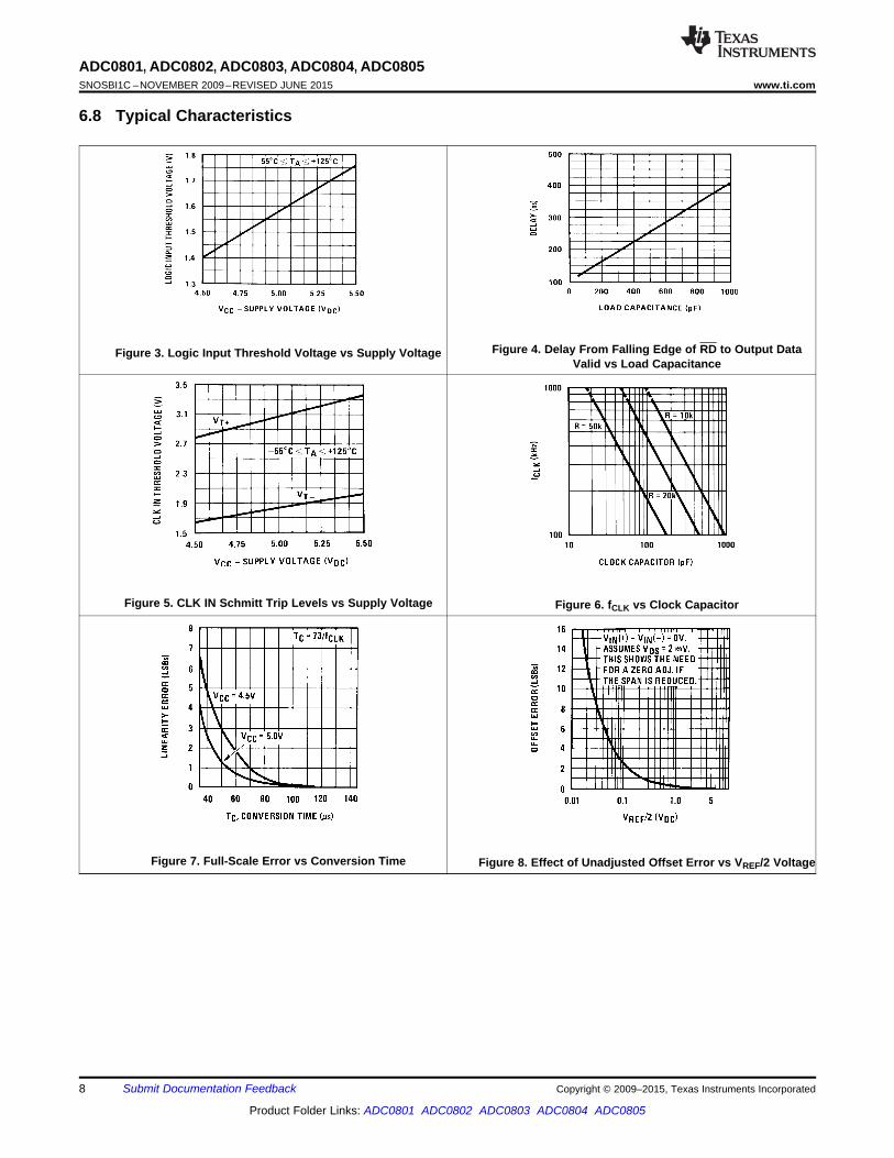
6.8 Typical Characteristics
Figure 4. Delay From Falling Edge of RD to Output DataFigure 3. Logic Input Threshold Voltage vs Supply VoltageValid vs Load Capacitance
Figure 5. CLK IN Schmitt Trip Levels vs Supply Voltage Figure 6. fCLK vs Clock Capacitor
Figure 7. Full-Scale Error vs Conversion Time Figure 8. Effect of Unadjusted Offset Error vs VREF/2 Voltage
8 Submit Documentation Feedback Copyright © 2009–2015, Texas Instruments Incorporated
Product Folder Links: ADC0801 ADC0802 ADC0803 ADC0804 ADC0805

ADC0801, ADC0802, ADC0803, ADC0804, ADC0805www.ti.com SNOSBI1C –NOVEMBER 2009–REVISED JUNE 2015
Typical Characteristics (continued)
Figure 10. Power Supply Current vs Temperature (1)Figure 9. Output Current vs Temperature
Figure 11. Linearity Error at Low VREF/2 Voltages
(1) The VREF/2 pin is the center point of a two-resistor divider connected from VCC to ground. In all versions of the ADC0801, ADC0802,ADC0803, and ADC0805, and in the ADC0804LCJ, each resistor is typically 16 kΩ. In all versions of the ADC0804 except theADC0804LCJ, each resistor is typically 2.2 kΩ.
Copyright © 2009–2015, Texas Instruments Incorporated Submit Documentation Feedback 9
Product Folder Links: ADC0801 ADC0802 ADC0803 ADC0804 ADC0805

ADC0801, ADC0802, ADC0803, ADC0804, ADC0805SNOSBI1C –NOVEMBER 2009–REVISED JUNE 2015 www.ti.com
7 Parameter Measurement Information
7.1 Tri-State Test Circuits and Waveforms
CL = 10 pF
Figure 12. RD to Data Output Falling Edge Test Figure 13. RD to Data Output Falling Edge TestLoad Condition Timing
CL = 10 pF
Figure 14. RD to Data Output Rising Edge Test Figure 15. RD to Data Output Rising Edge TestLoad Condition Timing
10 Submit Documentation Feedback Copyright © 2009–2015, Texas Instruments Incorporated
Product Folder Links: ADC0801 ADC0802 ADC0803 ADC0804 ADC0805

ADC0801, ADC0802, ADC0803, ADC0804, ADC0805www.ti.com SNOSBI1C –NOVEMBER 2009–REVISED JUNE 2015
8 Detailed Description
8.1 OverviewThe ADC0801 series are versatile 8-Bit µP compatible general purpose ADC converters operate on single 5-Vsupply. These devices are treated as a memory location or I/O port to a micro-processor system withoutadditional interface logic. The outputs are Tri-state latched which facilitate interfacing to micro-processor controlbus. The converter is designed with a differential potentiometric ladder, a circuit equivalent of the 256R network.It contains analog switches sequenced by successive approximation logic. A functional diagram of the ADCconverter is shown in Functional Block Diagram. All of the package pinouts are shown and the major logic controlpaths are drawn in heavier weight lines. The differential analog voltage input has good common mode-rejectionand permits offsetting the analog zero-input voltage value. Moreover, the input reference voltage can be adjustedto allow encoding small analog voltage span to the full 8-bits resolution. To ensure start-up under all possibleconditions, an external WR pulse is required during the first power-up cycle.
Using a SAR logic the most significant bit is tested first and after 8 comparisons (64 clock cycles) a digital 8-bitbinary code (1111 1111 = full-scale) is transferred to an output latch and then an interrupt is asserted (INTRmakes a high-to-low transition). A conversion in process can be interrupted by issuing a second start command.The device may be operated in the free-running mode by connecting INTR to the WR input with CS=0.
On the high-to-low transition of the WR input the internal SAR latches and the shift register stages are reset. Aslong as the CS input and WR input remain low, the ADC will remain in a reset state. Conversion will start from 1to 8 clock periods after at least one of these inputs makes a low-to-high transition.
The converter is started by having CS and WR simultaneously low. This sets the start flip-flop (F/F) and theresulting “1” level resets the 8-bit shift register, resets the Interrupt (INTR) F/F and inputs a “1” to the D flop,F/F1, which is at the input end of the 8-bit shift register. Internal clock signals then transfer this “1” to the Qoutput of F/F1. The AND gate, G1, combines this “1” output with a clock signal to provide a reset signal to thestart F/F. If the set signal is no longer present (either WR or CS is a “1”) the start F/F is reset and the 8-bit shiftregister then can have the “1” clocked in, which starts the conversion process. If the set signal were to still bepresent, this reset pulse would have no effect (both outputs of the start F/F would momentarily be at a “1” level)and the 8-bit shift register would continue to be held in the reset mode. This logic therefore allows for wide CSand WR signals and the converter will start after at least one of these signals returns high and the internal clocksagain provide a reset signal for the start F/F.
After the “1” is clocked through the 8-bit shift register (which completes the SAR search) it appears as the inputto the D-type latch, LATCH 1. As soon as this “1” is output from the shift register, the AND gate, G2, causes thenew digital word to transfer to the Tri-state output latches. When LATCH 1 is subsequently enabled, the Q outputmakes a high-to-low transition which causes the INTR F/F to set. An inverting buffer then supplies the INTR inputsignal.
Note this SET control of the INTR F/F remains low for 8 of the external clock periods (as the internal clocks runat 1/8 of the frequency of the external clock). If the data output is continuously enabled (CS and RD both heldlow), the INTR output will still signal the end of conversion (by a high-to-low transition), because the SET inputcan control the Q output of the INTR F/F even though the RESET input is constantly at a M "1M " level in thisoperating mode. This INTR output will therefore stay low for the duration of the SET signal, which is 8 periods ofthe external clock frequency (assuming the ADC is not started during this interval).
When operating in the free-running or continuous conversion mode (INTR pin tied to WR and CS wired low – seeContinuous Conversions), the START F/F is SET by the high-to-low transition of the INTR signal. This resets theSHIFT REGISTER which causes the input to the D-type latch, LATCH 1, to go low. As the latch enable input isstill present, the Q output will go high, which then allows the INTR F/F to be RESET. This reduces the width ofthe resulting INTR output pulse to only a few propagation delays (approximately 300 ns).
When data is to be read, the combination of both CS and RD being low will cause the INTR F/F to be reset andthe Tri-state output latches will be enabled to provide the 8-bit digital outputs.
Copyright © 2009–2015, Texas Instruments Incorporated Submit Documentation Feedback 11
Product Folder Links: ADC0801 ADC0802 ADC0803 ADC0804 ADC0805

ADC0801, ADC0802, ADC0803, ADC0804, ADC0805SNOSBI1C –NOVEMBER 2009–REVISED JUNE 2015 www.ti.com
8.2 Functional Block Diagram
(1) CS shown twice for clarity.(2) SAR = Successive Approximation Register.
8.3 Feature Description
8.3.1 Understanding ADC Error SpecsA perfect ADC transfer characteristic (staircase waveform) is shown in Figure 16 and Figure 17. The horizontalscale is analog input voltage and the particular points labeled are in steps of 1 LSB (19.53 mV with 2.5V tied tothe VREF/2 pin). The digital output codes that correspond to these inputs are shown as D−1, D, and D+1. Forthe perfect ADC, not only will center- value (A−1, A, A+1, . . . . ) analog inputs produce the cor- rect output digitalcodes, but also each riser (the transitions between adjacent output codes) will be located ±1⁄2 LSB away fromeach center-value. As shown, the risers are ideal and have no width. Correct digital output codes will be providedfor a range of analog input voltages that extend ±1⁄2 LSB from the ideal center-values. Each tread (the range ofanalog input voltage that provides the same digital output code) is therefore 1 LSB wide.
Figure 19 shows a worst case error plot for the ADC0801. All center-valued inputs are guaranteed to produce thecorrect output codes and the adjacent risers are specified to be no closer to the center-value points than ±1/4LSB. In other words, if we apply an analog input equal to the center-value ±1/4 LSB, we guarantee that the ADCwill produce the correct digital code. The maximum range of the position of the code transition is indicated by thehorizontal arrow and it is specified to be no more than 1/2 LSB.
The error curve of Figure 21 shows a worst case error plot for the ADC0802. Here we guarantee that if we applyan analog input equal to the LSB analog voltage center-value the ADC will produce the correct digital code.
12 Submit Documentation Feedback Copyright © 2009–2015, Texas Instruments Incorporated
Product Folder Links: ADC0801 ADC0802 ADC0803 ADC0804 ADC0805

ADC0801, ADC0802, ADC0803, ADC0804, ADC0805www.ti.com SNOSBI1C –NOVEMBER 2009–REVISED JUNE 2015
Feature Description (continued)Next to each transfer function is shown the corresponding error plot. Many people may be more familiar witherror plots than transfer functions. The analog input voltage to the ADC is provided by either a linear ramp or bythe discrete output steps of a high resolution DAC. Notice that the error is continuously displayed and includesthe quantization uncertainty of the ADC. For example the error at point 1 of Figure 21 is +1⁄2 LSB because thedigital code appeared 1⁄2 LSB in advance of the center-value of the tread. The error plots always have aconstant negative slope and the abrupt up-side steps are always 1 LSB in magnitude.
Figure 17. Clarifying the Error Specs of an ADC ConverterFigure 16. Transfer Function of Analog Input vs DigitalAccuracy=±0 LSB: A Perfect ADCOutput Code in Ideal ADC
Figure 18. Transfer Function of Analog Input vs Digital Figure 19. Clarifying the Error Specs of an ADC ConverterOutput Code for ±1/4 LSB Accuracy ADC Accuracy =±1⁄4 LSB
Figure 20. Transfer Function of Analog Input vs Digital Figure 21. Clarifying the Error Specs of an ADC ConverterOutput Code for ±1/2 LSB Accuracy ADC Accuracy = ±1⁄2 LSB
Copyright © 2009–2015, Texas Instruments Incorporated Submit Documentation Feedback 13
Product Folder Links: ADC0801 ADC0802 ADC0803 ADC0804 ADC0805

ADC0801, ADC0802, ADC0803, ADC0804, ADC0805SNOSBI1C –NOVEMBER 2009–REVISED JUNE 2015 www.ti.com
Feature Description (continued)8.3.2 Digital Control InputsThe digital control inputs (CS, RD, and WR) meet standard TLL logic voltage levels. These signals have beenrenamed when compared to the standard ADC Start and Output Enable labels. In addition, these inputs areactive low to allow an easy interface to microprocessor control busses. For non-microprocessor basedapplications, the CS input (pin 1) can be grounded and the standard ADC Start function is obtained by an activelow pulse applied at the WR input (pin 3) and the Output Enable function is caused by an active low pull at theRD input (pin 2).
8.4 Device Functional Modes
8.4.1 Analog Input Modes
8.4.1.1 Normal ModeDue to the internal switching action, displacement currents will flow at the analog inputs. This is due to on-chipstray capacitance to ground as shown in Figure 22.
rON of SW 1 and SW 2.5 kΩr=rON CSTRAY × 5 kΩ x 12 pF = 60 ns
Figure 22. Analog Input Impedance
The voltage on this capacitance is switched and will result in currents entering the VIN(+) input pin and leavingthe VIN(−) input which will depend on the analog differential input voltage levels. These current transients occurat the leading edge of the internal clocks. They rapidly decay and do not cause errors as the on-chip comparatoris strobed at the end of the clock period.
8.4.1.2 Fault ModeIf the voltage source applied to the VIN(+) or VIN(−) pin exceeds the allowed operating range of VCC+50 mV, largeinput currents can flow through a parasitic diode to the VCC pin. If these currents can exceed the 1 mA maxallowed spec, an external diode (1N914) should be added to bypass this current to the VCC pin (with the currentbypassed with this diode, the voltage at the VIN(+) pin can exceed the VCC voltage by the forward voltage of thisdiode).
14 Submit Documentation Feedback Copyright © 2009–2015, Texas Instruments Incorporated
Product Folder Links: ADC0801 ADC0802 ADC0803 ADC0804 ADC0805

ADC0801, ADC0802, ADC0803, ADC0804, ADC0805www.ti.com SNOSBI1C –NOVEMBER 2009–REVISED JUNE 2015
9 Application and Implementation
NOTEInformation in the following applications sections is not part of the TI componentspecification, and TI does not warrant its accuracy or completeness. TI’s customers areresponsible for determining suitability of components for their purposes. Customers shouldvalidate and test their design implementation to confirm system functionality.
9.1 Application InformationThe following sections give example circuits and suggestions for using the ADC080X in typical applicationsituation with a typical 8-bit micro-processor.
9.1.1 Testing the ADC ConverterThere are many degrees of complexity associated with testing an ADC converter. One of the simplest tests is toapply a known analog input voltage to the converter and use LEDs to display the resulting digital output code asshown in Figure 23.
For ease of testing, the VREF/2 (pin 9) should be supplied with 2.560 VDC and a VCC supply voltage of 5.12 VDCshould be used. This provides an LSB value of 20 mV.
If a full-scale adjustment is to be made, an analog input voltage of 5.090 VDC (5.120–1/⁄2 LSB) should be appliedto the VIN(+) pin with the VIN(−) pin grounded. The value of the VREF/2 input voltage should then be adjusted untilthe digital output code is just changing from 1111 1110 to 1111 1111. This value of VREF/2 should then be usedfor all the tests.
The digital output LED display can be decoded by dividing the 8 bits into 2 hex characters, the 4 most significant(MS) and the 4 least significant (LS). Table 1 shows the fractional binary equivalent of these two 4-bit groups. Byadding the voltages obtained from the "VM" and "VLS" columns in Table 1, the nominal value of the digitaldisplay (when VREF/2 = 2.560V) can be determined. For example, for an output LED display of 1011 0110 or B6(in hex), the voltage values from the table are 3.520 + 0.120 or 3.640 VDC. These voltage values represent thecenter-values of a perfect ADC converter. The effects of quantization error have to be accounted for in theinterpretation of the test results.
Copyright © 2009–2015, Texas Instruments Incorporated Submit Documentation Feedback 15
Product Folder Links: ADC0801 ADC0802 ADC0803 ADC0804 ADC0805

ADC0801, ADC0802, ADC0803, ADC0804, ADC0805SNOSBI1C –NOVEMBER 2009–REVISED JUNE 2015 www.ti.com
Application Information (continued)
Figure 23. Basic ADC Tester
For a higher speed test system, or to obtain plotted data, a digital-to-analog converter is needed for the test set-up. An accurate 10-bit DAC can serve as the precision voltage source for the ADC. Errors of the ADC under testcan be expressed as either analog voltages or differences in 2 digital words.
A basic ADC tester that uses a DAC and provides the error as an analog output voltage is shown in Figure 35.The 2 op amps can be eliminated if a lab DVM with a numerical subtraction feature is available to read thedifference voltage, "A–C", directly. The analog input voltage can be supplied by a low frequency ramp generatorand an X-Y plotter can be used to provide analog error (Y axis) versus analog input (X axis).
For operation with a microprocessor or a computer-based test system, it is more convenient to present the errorsdigitally. This can be done with the circuit of Figure 25, where the output code transitions can be detected as the10-bit DAC is incremented. This provides 1⁄4 LSB steps for the 8-bit ADC under test. If the results of this test areautomatically plotted with the analog input on the X axis and the error (in LSB’s) as the Y axis, a useful transferfunction of the ADC under test results. For acceptance testing, the plot is not necessary and the testing speedcan be increased by establishing internal limits on the allowed error for each code.
9.1.2 Microprocessor InterfacingTo discuss the interface with 8080A and 6800 microprocessors, a common sample subroutine structure is used.The microprocessor starts the ADC, reads and stores the results of 16 successive conversions, then returns tothe user’s program. The 16 data bytes are stored in 16 successive memory locations. All Data and Addresseswill be given in hexadecimal form. Software and hardware details are provided separately for each type ofmicroprocessor.
16 Submit Documentation Feedback Copyright © 2009–2015, Texas Instruments Incorporated
Product Folder Links: ADC0801 ADC0802 ADC0803 ADC0804 ADC0805

ADC0801, ADC0802, ADC0803, ADC0804, ADC0805www.ti.com SNOSBI1C –NOVEMBER 2009–REVISED JUNE 2015
Application Information (continued)9.1.2.1 Interfacing 8080 Microprocessor Derivatives (8048, 8085)This converter has been designed to directly interface with derivatives of the 8080 microprocessor. The ADC canbe mapped into memory space (using standard memory address decoding for CS and the MEMR and MEMWstrobes) or it can be controlled as an I/O device by using the I/O R and I/O W strobes and decoding the addressbits A0 → A7 (or address bits A8 → A15 as they will contain the same 8-bit address information) to obtain theCS input. Using the I/O space provides 256 additional addresses and may allow a simpler 8-bit address decoderbut the data can only be input to the accumulator. To make use of the additional memory reference instructions,the ADC should be mapped into memory space. An example of an ADC in I/O space is shown in Figure 26.
Figure 24. ADC Tester with Analog Error Output
Figure 25. Basic “Digital” ADC Tester
Table 1. Decoding the Digital Output LEDsOUTPUT VOLTAGE CENTER VALUESFRACTIONAL BINARY VALUE FOR WITH VREF/2=2.560 VDCHEX BINARY
MS GROUP LS GROUP VMS GROUP (1) VLS GROUP (1)
F 1 1 1 1 15/16 15/256 4.800 0.300
E 1 1 1 0 7/8 7/128 4.480 0.280
D 1 1 0 1 13/16 13/256 4.160 0.260
C 1 1 0 0 3/4 3/64 3.840 0.240
B 1 0 1 1 11/16 11/256 3.520 0.220
(1) Display Output=VMS Group + VLS Group
Copyright © 2009–2015, Texas Instruments Incorporated Submit Documentation Feedback 17
Product Folder Links: ADC0801 ADC0802 ADC0803 ADC0804 ADC0805

ADC0801, ADC0802, ADC0803, ADC0804, ADC0805SNOSBI1C –NOVEMBER 2009–REVISED JUNE 2015 www.ti.com
Application Information (continued)Table 1. Decoding the Digital Output LEDs (continued)
OUTPUT VOLTAGE CENTER VALUESFRACTIONAL BINARY VALUE FOR WITH VREF/2=2.560 VDCHEX BINARYMS GROUP LS GROUP VMS GROUP (1) VLS GROUP (1)
A 1 0 1 0 5/8 5/128 3.200 0.200
9 1 0 0 1 9/16 9/256 2.880 0.180
8 1 0 0 0 1/2 1/32 2.560 0.160
7 0 1 1 1 7/16 7/256 2.240 0.140
6 0 1 1 0 3/8 3/128 1.920 0.120
5 0 1 0 1 5/16 2/256 1.600 0.100
4 0 1 0 0 1/4 1/64 1.280 0.080
3 0 0 1 1 163 3/256 0.960 0.060
2 0 0 1 0 1/8 1/128 0.640 0.040
1 0 0 0 1 1/16 1/256 0.320 0.020
0 0 0 0 0 0 0
(1) *Pin numbers for the DP8228 system controller, others are INS8080A(2) Pin 23 of the INS8228 must be tied to +12V through a 1 kΩ resistor to generate the RST 7 instruction when an
interrupt is acknowledged as required by the accompanying sample program.
Figure 26. ADC0801_INS8080A CPU Interface
18 Submit Documentation Feedback Copyright © 2009–2015, Texas Instruments Incorporated
Product Folder Links: ADC0801 ADC0802 ADC0803 ADC0804 ADC0805

ADC0801, ADC0802, ADC0803, ADC0804, ADC0805www.ti.com SNOSBI1C –NOVEMBER 2009–REVISED JUNE 2015
Note: The stack pointer must be dimensioned because a RST 7 instruction pushes the PC onto the stack.Note: All address used were arbitrarily chosen.
Figure 27. Sample Program for Figure 26 ADC0801–INS8080A CPU Interface
The standard control bus signals of the 8080 CS, RD and WR) can be directly wired to the digital control inputsof the ADC and the bus timing requirements are met to allow both starting the converter and outputting the dataonto the data bus. A bus driver should be used for larger microprocessor systems where the data bus leaves thePCB and/or must drive capacitive loads larger than 100 pF.
9.1.2.2 Sample 8080A CPU Interfacing Circuitry and ProgramThe following sample program and associated hardware shown in Figure 26 may be used to input data from theconverter to the INS8080A CPU chip set (comprised of the INS8080A microprocessor, the INS8228 systemcontroller and the INS8224 clock generator). For simplicity, the ADC is controlled as an I/O device, specifically an8-bit bi-directional port located at an arbitrarily chosen port address, E0. The Tri-state output capability of theADC eliminates the need for a peripheral interface device, however address decoding is still required to generatethe appropriate CS for the converter.
It is important to note in systems where the ADC converter is 1-of-8 or less I/O mapped devices, no addressdecoding circuitry is necessary. Each of the 8 address bits (A0 to A7) can be directly used as CS inputs — onefor each I/O device.
9.1.2.3 INS8048 InterfaceThe INS8048 interface technique with the ADC0801 series (see Figure 28) is simpler than the 8080A CPUinterface. There are 24 I/O lines and three test input lines in the 8048. With these extra I/O lines available, one ofthe I/O lines (bit 0 of port 1) is used as the chip select signal to the ADC, thus eliminating the use of an externaladdress decoder. Bus control signals RD, WR and INT of the 8048 are tied directly to the ADC. The 16converted data words are stored at on-chip RAM locations from 20 to 2F (Hex). The RD and WR signals aregenerated by reading from and writing into a dummy address, respectively. A sample interface program is shownbelow.
Copyright © 2009–2015, Texas Instruments Incorporated Submit Documentation Feedback 19
Product Folder Links: ADC0801 ADC0802 ADC0803 ADC0804 ADC0805

ADC0801, ADC0802, ADC0803, ADC0804, ADC0805SNOSBI1C –NOVEMBER 2009–REVISED JUNE 2015 www.ti.com
Figure 28. INS8048 Interface
Figure 29. Sample Program for Figure 28 INS8048 Interface
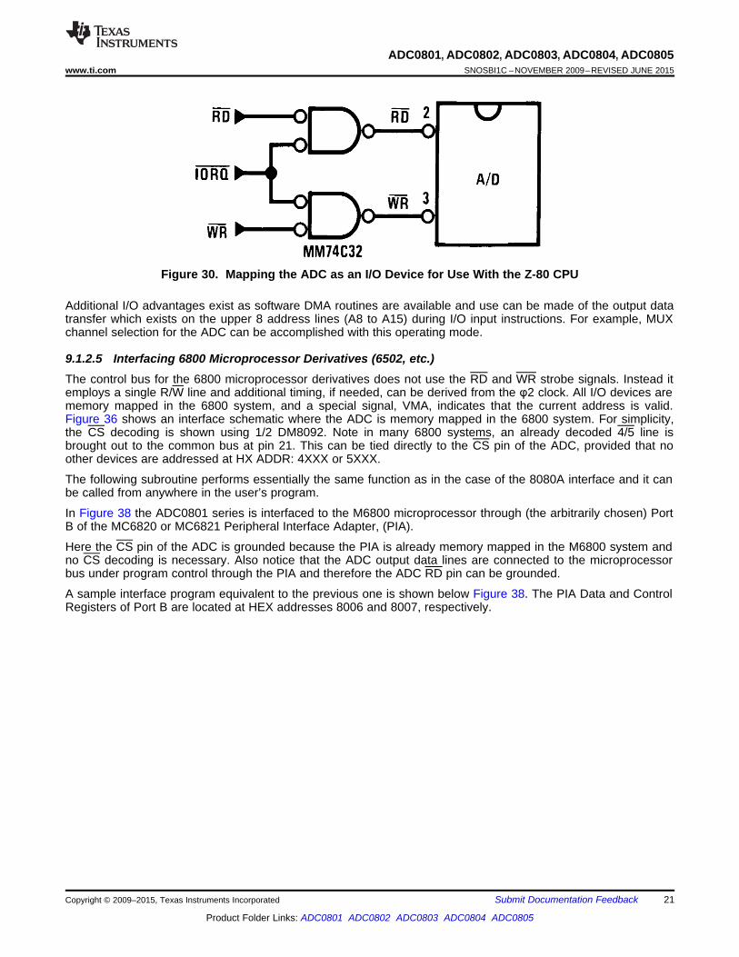
9.1.2.4 Interfacing the Z-80The Z-80 control bus is slightly different from that of the 8080. General RD and WR strobes are provided andseparate memory request, MREQ, and I/O request, IORQ, signals are used which have to be combined with thegeneralized strobes to provide the equivalent 8080 signals. An advantage of operating the ADC in I/O space withthe Z-80 is that the CPU will automatically insert one wait state (the RD and WR strobes are extended one clockperiod) to allow more time for the I/O devices to respond. Logic to map the ADC in I/O space is shown inFigure 30.
20 Submit Documentation Feedback Copyright © 2009–2015, Texas Instruments Incorporated
Product Folder Links: ADC0801 ADC0802 ADC0803 ADC0804 ADC0805
ADC0801, ADC0802, ADC0803, ADC0804, ADC0805www.ti.com SNOSBI1C –NOVEMBER 2009–REVISED JUNE 2015
Figure 30. Mapping the ADC as an I/O Device for Use With the Z-80 CPU
Additional I/O advantages exist as software DMA routines are available and use can be made of the output datatransfer which exists on the upper 8 address lines (A8 to A15) during I/O input instructions. For example, MUXchannel selection for the ADC can be accomplished with this operating mode.
9.1.2.5 Interfacing 6800 Microprocessor Derivatives (6502, etc.)The control bus for the 6800 microprocessor derivatives does not use the RD and WR strobe signals. Instead itemploys a single R/W line and additional timing, if needed, can be derived from the φ2 clock. All I/O devices arememory mapped in the 6800 system, and a special signal, VMA, indicates that the current address is valid.Figure 36 shows an interface schematic where the ADC is memory mapped in the 6800 system. For simplicity,the CS decoding is shown using 1/2 DM8092. Note in many 6800 systems, an already decoded 4/5 line isbrought out to the common bus at pin 21. This can be tied directly to the CS pin of the ADC, provided that noother devices are addressed at HX ADDR: 4XXX or 5XXX.
The following subroutine performs essentially the same function as in the case of the 8080A interface and it canbe called from anywhere in the user’s program.
In Figure 38 the ADC0801 series is interfaced to the M6800 microprocessor through (the arbitrarily chosen) PortB of the MC6820 or MC6821 Peripheral Interface Adapter, (PIA).
Here the CS pin of the ADC is grounded because the PIA is already memory mapped in the M6800 system andno CS decoding is necessary. Also notice that the ADC output data lines are connected to the microprocessorbus under program control through the PIA and therefore the ADC RD pin can be grounded.
A sample interface program equivalent to the previous one is shown below Figure 38. The PIA Data and ControlRegisters of Port B are located at HEX addresses 8006 and 8007, respectively.
Copyright © 2009–2015, Texas Instruments Incorporated Submit Documentation Feedback 21
Product Folder Links: ADC0801 ADC0802 ADC0803 ADC0804 ADC0805

ADC0801, ADC0802, ADC0803, ADC0804, ADC0805SNOSBI1C –NOVEMBER 2009–REVISED JUNE 2015 www.ti.com
9.2 Typical Applications
9.2.1 8080 Interface
Figure 31. Generic Interface Between ADC and 8-Bit µPs
ERROR SPECIFICATION (Includes Full-Scale, Zero Error, and Non-Linearity)VREF/2 = 2.500 VDC VREF/2 = No ConnectionFULL-SCALEPART NUMBER ADJUSTED (No Adjustments) (No Adjustments)
ADC0801 ±1⁄4 LSBADC0802 ±1⁄2 LSBADC0803 ±1⁄2 LSBADC0804 ±1 LSBADC0805 ±1 LSB
9.2.1.1 Design RequirementsFor these example applications, the input analog signal is differential to illustrate the offset and common modereduction merits. An example of the use of an adjusted reference voltage is to accommodate a reduced span ordynamic voltage range of the analog input voltage is also depicted.
22 Submit Documentation Feedback Copyright © 2009–2015, Texas Instruments Incorporated
Product Folder Links: ADC0801 ADC0802 ADC0803 ADC0804 ADC0805

ADC0801, ADC0802, ADC0803, ADC0804, ADC0805www.ti.com SNOSBI1C –NOVEMBER 2009–REVISED JUNE 2015
Table 2. Design ParametersPARAMETER EXAMPLE VALUE
ADC clock frequency, FCLK 640 KHzInput source resistance, RIN 100 Ω
9.2.1.2 Detailed Design Procedure
9.2.1.2.1 Analog Differential Voltage Inputs and Common-Mode Rejection
This ADC has additional applications flexibility due to the analog differential voltage input. The VIN(−) input (pin 7)can be used to automatically subtract a fixed voltage value from the input reading (tare correction). This is alsouseful in 4 mA–20 mA current loop conversion. In addition, common-mode noise can be reduced by use of thedifferential input.
The time interval between sampling VIN(+) and VIN(−) is 4-1/2 clock periods. The maximum error voltage due tothis slight time difference between the input voltage samples is given by:
where• ∆Ve is the error voltage due to sampling delay• VP is the peak value of the common-mode voltage• fcm is the common-mode frequency (1)
As an example, to keep this error to 1/4 LSB (∼5 mV) when operating with a 60 Hz common-mode frequency,fcm, and using a 640 kHz ADC clock, fCLK, would allow a peak value of the common-mode voltage, VP, which isgiven by:
(2)
or
(3)
which gives VP–1.9 V.
The allowed range of analog input voltages usually places more severe restrictions on input common-mode noiselevels.
An analog input voltage with a reduced span and a relatively large zero offset can be handled easily by makinguse of the differential input (see Reference Voltage).
9.2.1.2.2 Analog Inputs — Input Current
9.2.1.2.2.1 Input Bypass Capacitors
Bypass capacitors at the inputs will average these charges and cause a DC current to flow through the outputresistances of the analog signal sources. This charge pumping action is worse for continuous conversions withthe VIN(+) input voltage at full-scale. For continuous conversions with a 640 kHz clock frequency with the VIN(+)input at 5V, this DC current is at a maximum of approximately 5 µA. Therefore, bypass capacitors should not beused at the analog inputs or the VREF/2 pin for high resistance sources (> 1 kΩ). If input bypass capacitors arenecessary for noise filtering and high source resistance is desirable to minimize capacitor size, the detrimentaleffects of the voltage drop across this input resistance, which is due to the average value of the input current,can be eliminated with a full-scale adjustment while the given source resistor and input bypass capacitor are bothin place. This is possible because the average value of the input current is a precise linear function of thedifferential input voltage.
Copyright © 2009–2015, Texas Instruments Incorporated Submit Documentation Feedback 23
Product Folder Links: ADC0801 ADC0802 ADC0803 ADC0804 ADC0805

ADC0801, ADC0802, ADC0803, ADC0804, ADC0805SNOSBI1C –NOVEMBER 2009–REVISED JUNE 2015 www.ti.com
9.2.1.2.2.2 Input Source Resistance
Large values of source resistance where an input bypass capacitor is not used, will not cause errors as the inputcurrents settle out prior to the comparison time. If a low pass filter is required in the system, use a low valuedseries resistor (≤ 1 kΩ) for a passive RC section or add an op amp RC active low pass filter. For low sourceresistance applications, (≤ 1 kΩ), a 0.1 μF bypass capacitor at the inputs will prevent noise pickup due to serieslead inductance of a long wire. A 100Ω series resistor can be used to isolate this capacitor — both the R and Care placed outside the feedback loop — from the output of an op amp, if used.
9.2.1.2.2.3 Noise
The leads to the analog inputs (pins 6 and 7) should be kept as short as possible to minimize input noisecoupling. Both noise and undesired digital clock coupling to these inputs can cause system errors. The sourceresistance for these inputs should, in general, be kept below 5 kΩ. Larger values of source resistance can causeundesired system noise pickup. Input bypass capacitors, placed from the analog inputs to ground, will eliminatesystem noise pickup but can create analog scale errors as these capacitors will average the transient inputswitching currents of the ADC (see Analog Inputs — Input Current). This scale error depends on both a largesource resistance and the use of an input bypass capacitor. This error can be eliminated by doing a full-scaleadjustment of the ADC (adjust VREF/2 for a proper full-scale reading — see Full-Scale) with the source resistanceand input bypass capacitor in place.
Noise spikes on the VCC supply line can cause conversion errors as the comparator will respond to this noise. Alow inductance tantalum filter capacitor should be used close to the converter VCC pin and values of 1 µF orgreater are recommended. If an unregulated voltage is available in the system, a separate LM340LAZ-5.0, TO-92, 5-V voltage regulator for the converter (and other analog circuitry) will greatly reduce digital noise on the VCCsupply.
9.2.1.2.3 Reference Voltage
9.2.1.2.3.1 Span Adjust
For maximum applications flexibility, these ADCs have been designed to accommodate a 5 VDC, 2.5 VDC or anadjusted voltage reference. This has been achieved in the design of the IC as shown in Figure 32.
Figure 32. The VREFERENCE Design on the IC
24 Submit Documentation Feedback Copyright © 2009–2015, Texas Instruments Incorporated
Product Folder Links: ADC0801 ADC0802 ADC0803 ADC0804 ADC0805

ADC0801, ADC0802, ADC0803, ADC0804, ADC0805www.ti.com SNOSBI1C –NOVEMBER 2009–REVISED JUNE 2015
Notice that the reference voltage for the IC is either 1/2 of the voltage applied to the VCC supply pin, or is equal tothe voltage that is externally forced at the VREF/2 pin. This allows for a ratiometric voltage reference using theVCC supply, a 5 VDC reference voltage can be used for the VCC supply or a voltage less than 2.5 VDC can beapplied to the VREF/2 input for increased application flexibility. The internal gain to the VREF/2 input is 2, makingthe full-scale differential input voltage twice the voltage at pin 9.
An example of the use of an adjusted reference voltage is to accommodate a reduced span — or dynamicvoltage range of the analog input voltage. If the analog input voltage were to range from 0.5 VDC to 3.5 VDC,instead of 0V to 5 VDC, the span would be 3 V as shown in Figure 33. With 0.5 VDC applied to the VIN(−) pin toabsorb the offset, the reference voltage can be made equal to 1/2 of the 3V span or 1.5 VDC. The ADC now willencode the VIN(+) signal from 0.5V to 3.5 V with the 0.5V input corresponding to zero and the 3.5 VDC inputcorresponding to full-scale. The full 8 bits of resolution are therefore applied over this reduced analog inputvoltage range.
9.2.1.2.3.2 Reference Accuracy Requirements
The converter can be operated in a ratiometric mode or an absolute mode. In ratiometric converter applications,the magnitude of the reference voltage is a factor in both the output of the source transducer and the output ofthe ADC converter and therefore cancels out in the final digital output code. The ADC0805 is specifiedparticularly for use in ratiometric applications with no adjustments required. In absolute conversion applications,both the initial value and the temperature stability of the reference voltage are important factors in the accuracyof the ADC converter. For VREF/2 voltages of 2.4 VDC nominal value, initial errors of ±10 mVDC will causeconversion errors of ±1 LSB due to the gain of 2 of the VREF/2 input. In reduced span applications, the initialvalue and the stability of the VREF/2 input voltage become even more important. For example, if the span isreduced to 2.5 V, the analog input LSB voltage value is correspondingly reduced from 20 mV (5V span) to 10 mVand 1 LSB at the VREF/2 input becomes 5 mV. As can be seen, this reduces the allowed initial tolerance of thereference voltage and requires correspondingly less absolute change with temperature variations. Note thatspans smaller than 2.5 V place even tighter requirements on the initial accuracy and stability of the referencesource.
In general, the magnitude of the reference voltage will require an initial adjustment. Errors due to an impropervalue of reference voltage appear as full-scale errors in the ADC transfer function. IC voltage regulators may beused for references if the ambient temperature changes are not excessive. The LM336B 2.5-V IC referencediode (from National Semiconductor) has a temperature stability of 1.8 mV typical (6 mV maximum) over0°C≤TA≤+70°C. Other temperature range parts are also available.
Figure 33. Analog Input Signal Example
Copyright © 2009–2015, Texas Instruments Incorporated Submit Documentation Feedback 25
Product Folder Links: ADC0801 ADC0802 ADC0803 ADC0804 ADC0805

ADC0801, ADC0802, ADC0803, ADC0804, ADC0805SNOSBI1C –NOVEMBER 2009–REVISED JUNE 2015 www.ti.com
*Add if VREF/2 ≤ 1 VDC with LM358 to draw 3 mA to ground.
Figure 34. Accommodating an Analog Input from 0.5V (Digital Out = 00HEX) to 3.5 V (Digital Out=FFHEX)
9.2.1.2.4 Errors and Reference Voltage Adjustments
9.2.1.2.4.1 Zero Error
The zero of the ADC does not require adjustment. If the minimum analog input voltage value, VIN(MIN), is notground, a zero offset can be done. The converter can be made to output 0000 0000 digital code for this minimuminput voltage by biasing the ADC VIN(−) input at this VIN(MIN) value (see Application Information). This uses thedifferential mode operation of the ADC.
The zero error of the ADC converter relates to the location of the first riser of the transfer function and can bemeasured by grounding the VIN(−) input and applying a small magnitude positive voltage to the VIN(+) input. Zeroerror is the difference between the actual DC input voltage that is necessary to just cause an output digital codetransition from 0000 0000 to 0000 0001 and the ideal 1/2 LSB value (1/2 LSB = 9.8 mV for VREF/2=2.500 VDC).
9.2.1.2.4.2 Full-Scale
The full-scale adjustment can be made by applying a differential input voltage that is 11/2 LSB less than thedesired analog full-scale voltage range and then adjusting the magnitude of the VREF/2 input (pin 9 or the VCCsupply if pin 9 is not used) for a digital output code that is just changing from 1111 1110 to 1111 1111.
26 Submit Documentation Feedback Copyright © 2009–2015, Texas Instruments Incorporated
Product Folder Links: ADC0801 ADC0802 ADC0803 ADC0804 ADC0805

- +
+ -
=é ùæ öæ ö-ê úç ÷ç ÷ç ÷ç ÷-ê úè øè øë û
@
CLK
CC T T
CC T T
1f
V V VRC ln
V V V
R 10 kΩ
ADC0801, ADC0802, ADC0803, ADC0804, ADC0805www.ti.com SNOSBI1C –NOVEMBER 2009–REVISED JUNE 2015
9.2.1.2.4.3 Adjusting for an Arbitrary Analog Input Voltage Range
If the analog zero voltage of the ADC is shifted away from ground (for example, to accommodate an analog inputsignal that does not go to ground) this new zero reference should be properly adjusted first. A VIN(+) voltage thatequals this desired zero reference plus 1/2 LSB (where the LSB is calculated for the desired analog span, 1LSB=analog span/256) is applied to pin 6 and the zero reference voltage at pin 7 should then be adjusted to justobtain the 00HEX to 01HEX code transition.
The full-scale adjustment should then be made (with the proper VIN(−) voltage applied) by forcing a voltage to theVIN(+) input which is given by:
where• VMAX = The high end of the analog input range• VMIN = the low end (the offset zero) of the analog range. (Both are ground referenced.) (4)
The VREF/2 (or VCC) voltage is then adjusted to provide a code change from FEHEX to FFHEX. This completes theadjustment procedure
9.2.1.2.5 Clocking Option
The clock for the ADC can be derived from the CPU clock or an external RC can be added to provide self-clocking. The CLK IN (pin 4) makes use of a Schmitt trigger as shown in Figure 35.
Figure 35. Self-Clocking the ADC
Heavy capacitive or DC loading of the clock R pin should be avoided as this will disturb normal converteroperation. Loads less than 50 pF, such as driving up to 7 ADC converter clock inputs from a single clock R pin of1 converter, are allowed. For larger clock line loading, a CMOS or low power TTL buffer or PNP input logicshould be used to minimize the loading on the clock R pin (do not use a standard TTL buffer).
Copyright © 2009–2015, Texas Instruments Incorporated Submit Documentation Feedback 27
Product Folder Links: ADC0801 ADC0802 ADC0803 ADC0804 ADC0805

ADC0801, ADC0802, ADC0803, ADC0804, ADC0805SNOSBI1C –NOVEMBER 2009–REVISED JUNE 2015 www.ti.com
9.2.1.2.6 Restart During a Conversion
If the ADC is restarted (CS and WR go low and return high) during a conversion, the converter is reset and anew conversion is started. The output data latch is not updated if the conversion in process is not allowed to becompleted, therefore the data of the previous conversion remains in this latch. The INTR output simply remainsat the “1” level.
9.2.1.2.7 Continuous Conversions
For operation in the free-running mode an initializing pulse should be used, following power up, to ensure circuitoperation. In this application, the CS input is grounded and the WR input is tied to the INTR output. This WR andINTR node should be momentarily forced to logic low following a power-up cycle to ensure operation.
9.2.1.2.8 Driving the Data Bus
This MOS ADC, like MOS microprocessors and memories, will require a bus driver when the total capacitance ofthe data bus gets large. Other circuitry, which is tied to the data bus, will add to the total capacitive loading, evenin Tri-state (high impedance mode). Backplane bussing also greatly adds to the stray capacitance of the databus.
There are some alternatives available to the designer to handle this problem. Basically, the capacitive loading ofthe data bus slows down the response time, even though DC specifications are still met. For systems operatingwith a relatively slow CPU clock frequency, more time is available in which to establish proper logic levels on thebus and therefore higher capacitive loads can be driven (see typical characteristics curves).
At higher CPU clock frequencies time can be extended for I/O reads (and/or writes) by inserting wait states(8080) or using clock extending circuits (6800).
Finally, if time is short and capacitive loading is high, external bus drivers must be used. These can be Tri-statebuffers (low power Schottky such as the DM74LS240 series is recommended) or special higher drive currentproducts which are designed as bus drivers. High current bipolar bus drivers with PNP inputs are recommended.
9.2.1.2.9 Wiring and Hook-Up Precautions
Standard digital wire wrap sockets are not satisfactory for breadboarding this ADC converter. Sockets on PCBscan be used and all logic signal wires and leads should be grouped and kept as far away as possible from theanalog signal leads. Exposed leads to the analog inputs can cause undesired digital noise and hum pickup,therefore shielded leads may be necessary in many applications.
A single point analog ground that is separate from the logic ground points should be used. The power supplybypass capacitor and the self-clocking capacitor (if used) should both be returned to digital ground. Any VREF/2bypass capacitors, analog input filter capacitors, or input signal shielding should be returned to the analogground point. A test for proper grounding is to measure the zero error of the ADC converter. Zero errors inexcess of 1/4 LSB can usually be traced to improper board layout and wiring (see Zero Error for measuring thezero error).
9.2.2 Multiple ADC0801 Series to MC6800 CPU InterfaceTo transfer analog data from several channels to a single microprocessor system, a multiple converter schemepresents several advantages over the conventional multiplexer single-converter approach. With the ADC0801series, the differential inputs allow individual span adjustment for each channel. Furthermore, all analog inputchannels are sensed simultaneously, which essentially divides the total system servicing time of themicroprocessor by the number of channels, because all conversions occur simultaneously. This scheme isshown in Figure 40.
28 Submit Documentation Feedback Copyright © 2009–2015, Texas Instruments Incorporated
Product Folder Links: ADC0801 ADC0802 ADC0803 ADC0804 ADC0805

ADC0801, ADC0802, ADC0803, ADC0804, ADC0805www.ti.com SNOSBI1C –NOVEMBER 2009–REVISED JUNE 2015
*Numbers in parentheses refer to MC6800 CPU pin out.**Number or letters in brackets refer to standard M6800 system common bus code.
Figure 36. ADC0801-MC6800 CPU Interface
In order for the microprocessor to service subroutines and inter- rupts, the stack pointer must be dimensioned in theuser’s program.
Figure 37. Sample Program for Figure 36 ADC0801-MC6800 CPU Interface
Copyright © 2009–2015, Texas Instruments Incorporated Submit Documentation Feedback 29
Product Folder Links: ADC0801 ADC0802 ADC0803 ADC0804 ADC0805

ADC0801, ADC0802, ADC0803, ADC0804, ADC0805SNOSBI1C –NOVEMBER 2009–REVISED JUNE 2015 www.ti.com
Figure 38. ADC0801–MC6820 PIA Interface
Figure 39. Sample Program for Figure 38 ADC0801–MC6820 PIA Interface
The following schematic and sample subroutine (DATA IN) in Auto-Zeroed Differential Transducer Amplifier andADC Converter section may be used to interface (up to) 8 ADC0801’s directly to the MC6800 CPU. This schemecan easily be extended to allow the interface of more converters. In this configuration the converters are(arbitrarily) located at HEX address 5000 in the MC6800 memory space. To save components, the clock signal isderived from just one RC pair on the first converter. This output drives the other ADCs.
30 Submit Documentation Feedback Copyright © 2009–2015, Texas Instruments Incorporated
Product Folder Links: ADC0801 ADC0802 ADC0803 ADC0804 ADC0805

ADC0801, ADC0802, ADC0803, ADC0804, ADC0805www.ti.com SNOSBI1C –NOVEMBER 2009–REVISED JUNE 2015
All the converters are started simultaneously with a STORE instruction at HEX address 5000. Note any otherHEX address of the form 5XXX will be decoded by the circuit, pulling all the CS inputs low. This can easily beavoided by using a more definitive address decoding scheme. All the interrupts are ORed together to insure thatall ADCs have completed their conversion before the microprocessor is interrupted.
The subroutine, DATA IN, may be called from anywhere in the user’s program. Once called, this routineinitializes the CPU, starts all the converters simultaneously and waits for the interrupt signal. Upon receiving theinterrupt, it reads the converters (from HEX addresses 5000 through 5007) and stores the data successively at(arbitrarily chosen) HEX addresses 0200 to 0207, before returning to the user’s pro- gram. All CPU registers thenrecover the original data they had before servicing DATA IN.
9.2.3 Auto-Zeroed Differential Transducer Amplifier and ADC ConverterThe differential inputs of the ADC0801 series eliminate the need to perform a differential to single endedconversion for a differential transducer. Thus, one op amp can be eliminated because the differential to singleended conversion is provided by the differential input of the ADC0801 series. In general, a transducer preamp isrequired to take advantage of the full ADC converter input dynamic range.
*Numbers in parentheses refer to MC6800 CPU pin out.**Numbers of letters in brackets refer to standard M6800 system common bus code.
Figure 40. Interfacing Multiple ADCs in an MC6800 System
Copyright © 2009–2015, Texas Instruments Incorporated Submit Documentation Feedback 31
Product Folder Links: ADC0801 ADC0802 ADC0803 ADC0804 ADC0805

ADC0801, ADC0802, ADC0803, ADC0804, ADC0805SNOSBI1C –NOVEMBER 2009–REVISED JUNE 2015 www.ti.com
Figure 41. Sample Program for Figure 40 Interfacing Multiple ADC’s in an MC6800 System
Figure 42. Sample Program for Figure 40 Interfacing Multiple ADC’s in an MC6800 System
Note: In order for the microprocessor to service subroutines and interrupts, the stack pointer must bedimensioned in the user’s program.
For amplification of DC input signals, a major system error is the input offset voltage of the amplifiers used forthe preamp. Figure 43 is a gain of 100 differential preamp whose offset voltage errors will be cancelled by azeroing subroutine which is performed by the INS8080A microprocessor system. The total allowable input offsetvoltage error for this preamp is only 50 µV for /⁄4 LSB error. This would obviously require very precise amplifiers.The expression for the differential output voltage of the preamp is:
32 Submit Documentation Feedback Copyright © 2009–2015, Texas Instruments Incorporated
Product Folder Links: ADC0801 ADC0802 ADC0803 ADC0804 ADC0805

ADC0801, ADC0802, ADC0803, ADC0804, ADC0805www.ti.com SNOSBI1C –NOVEMBER 2009–REVISED JUNE 2015
R2 = 49.5 R1Switches are LMC13334 CMOS analog switches.The 9 resistors used in the auto-zero section can be ±5% tolerance.
Figure 43. Gain of 100 Differential Transducer Preamp
where• IX is the current through resistor RX (5)
All of the offset error terms can be cancelled by making ±IXRX= VOS1 + VOS3 − VOS2. This is the principle of thisauto-zeroing scheme.
The INS8080A uses the 3 I/O ports of an INS8255 Programable Peripheral Interface (PPI) to control the autozeroing and input data from the ADC0801 as shown in Figure 44. The PPI is programmed for basic I/O operation(mode 0) with Port A being an input port and Ports B and C being output ports. Two bits of Port C are used toalternately open or close the 2 switches at the input of the preamp. Switch SW1 is closed to force the preamp’sdifferential input to be zero during the zeroing subroutine and then opened and SW2 is then closed forconversion of the actual differential input signal. Using 2 switches in this manner eliminates concern for the ONresistance of the switches as they must conduct only the input bias current of the input amplifiers.
Copyright © 2009–2015, Texas Instruments Incorporated Submit Documentation Feedback 33
Product Folder Links: ADC0801 ADC0802 ADC0803 ADC0804 ADC0805

ADC0801, ADC0802, ADC0803, ADC0804, ADC0805SNOSBI1C –NOVEMBER 2009–REVISED JUNE 2015 www.ti.com
Output Port B is used as a successive approximation register by the 8080 and the binary scaled resistors inseries with each output bit create a D/A converter. During the zeroing subroutine, the voltage at Vx increases ordecreases as required to make the differential output voltage equal to zero. This is accomplished by ensuringthat the voltage at the output of A1 is approximately 2.5V so that a logic "1" (5V) on any output of Port B willsource current into node VX thus raising the voltage at VX and making the output differential more negative.Conversely, a logic "0" (0V) will pull current out of node VX and decrease the voltage, causing the differentialoutput to become more positive. For the resistor values shown, VX can move ±12 mV with a resolution of 50 µV,which will null the offset error term to /⁄4 LSB of full-scale for the ADC0801. It is important that the voltage levelsthat drive the auto-zero resistors be constant. Also, for symmetry, a logic swing of 0V to 5V is convenient. Toachieve this, a CMOS buffer is used for the logic output signals of Port B and this CMOS package is poweredwith a stable 5V source. Buffer amplifier A1 is necessary so that it can source or sink the D/A output current.
Figure 44. Microprocessor Interface Circuitry for Differential Preamp
A flow chart for the zeroing subroutine is shown in Figure 45. It must be noted that the ADC0801 series willoutput an all zero code when it converts a negative input [VIN(−) ≥ VIN(+)]. Also, a logic inversion exists as all ofthe I/O ports are buffered with inverting gates.
Basically, if the data read is zero, the differential output voltage is negative, so a bit in Port B is cleared to pull VXmore negative which will make the output more positive for the next conversion. If the data read is not zero, theoutput voltage is positive so a bit in Port B is set to make VX more positive and the output more negative. Thiscontinues for 8 approximations and the differential output eventually converges to within 5 mV of zero.
The actual program is given in Figure 46. All addresses used are compatible with the BLC 80/10 microcomputersystem. In particular:
34 Submit Documentation Feedback Copyright © 2009–2015, Texas Instruments Incorporated
Product Folder Links: ADC0801 ADC0802 ADC0803 ADC0804 ADC0805

ADC0801, ADC0802, ADC0803, ADC0804, ADC0805www.ti.com SNOSBI1C –NOVEMBER 2009–REVISED JUNE 2015
• Port A and the ADC0801 are at port address E4• Port B is at port address E5• Port C is at port address E6• PPI control word port is at port address E7• Program Counter automatically goes to ADDR:3C3D upon acknowledgment of an interrupt from the ADC0801
9.2.4 Multiple ADC Converters in a Z-80 Interrupt Driven ModeIn data acquisition systems where more than one ADC converter (or other peripheral device) will be interruptingpro- gram execution of a microprocessor, there is obviously a need for the CPU to determine which devicerequires servicing. Figure 47 and the accompanying software is a method of determining which of 7 ADC0801converters has completed a conversion (INTR asserted) and is requesting an interrupt. This circuit allows startingthe ADC converters in any sequence, but will input and store valid data from the converters with a prioritysequence of ADC 1 being read first, ADC 2 second, etc., through ADC 7 which would have the lowest priority fordata being read. Only the converters whose INT is asserted will be read.
The key to decoding circuitry is the DM74LS373, 8-bit D type flip-flop. When the Z-80 acknowledges theinterrupt, the program is vectored to a data input Z-80 subroutine. This subroutine will read a peripheral statusword from the DM74LS373 which contains the logic state of the INTR outputs of all the converters. Eachconverter which initiates an interrupt will place a logic "0" in a unique bit position in the status word and thesubroutine will determine the identity of the converter and execute a data read. An identifier word (whichindicates which ADC the data came from) is stored in the next sequential memory location above the location ofthe data so the program can keep track of the identity of the data entered.
Copyright © 2009–2015, Texas Instruments Incorporated Submit Documentation Feedback 35
Product Folder Links: ADC0801 ADC0802 ADC0803 ADC0804 ADC0805

ADC0801, ADC0802, ADC0803, ADC0804, ADC0805SNOSBI1C –NOVEMBER 2009–REVISED JUNE 2015 www.ti.com
Figure 45. Flow Chart for Auto-Zero Routine
36 Submit Documentation Feedback Copyright © 2009–2015, Texas Instruments Incorporated
Product Folder Links: ADC0801 ADC0802 ADC0803 ADC0804 ADC0805

ADC0801, ADC0802, ADC0803, ADC0804, ADC0805www.ti.com SNOSBI1C –NOVEMBER 2009–REVISED JUNE 2015
NOTE: All numerical values are hexadecimal representations.
Figure 46. Software for Auto-Zeroed Differential ADC
The following notes apply:• It is assumed that the CPU automatically performs a RST 7 instruction when a valid interrupt is acknowledged
(CPU is in interrupt mode 1). Hence, the subroutine starting address of X0038.• The address bus from the Z-80 and the data bus to the Z-80 are assumed to be inverted by bus drivers.• ADC data and identifying words will be stored in sequential memory locations starting at the arbitrarily chosen
address X 3E00.• The stack pointer must be dimensioned in the main program as the RST 7 instruction automatically pushes
the PC onto the stack and the subroutine uses an additional 6 stack addresses.• The peripherals of concern are mapped into I/O space with the following port assignments:
Table 3. Port Assignment Where Peripherals are Mapped into I/O SpaceHEX PORT ADDRESS PERIPHERAL HEX PORT ADDRESS PERIPHERAL
00 MM74C374 8-bit flip-flop 04 ADC 401 ADC 1 05 ADC 5
Copyright © 2009–2015, Texas Instruments Incorporated Submit Documentation Feedback 37
Product Folder Links: ADC0801 ADC0802 ADC0803 ADC0804 ADC0805

ADC0801, ADC0802, ADC0803, ADC0804, ADC0805SNOSBI1C –NOVEMBER 2009–REVISED JUNE 2015 www.ti.com
Table 3. Port Assignment Where Peripherals are Mapped into I/O Space (continued)HEX PORT ADDRESS PERIPHERAL HEX PORT ADDRESS PERIPHERAL
02 ADC 2 06 ADC 603 ADC 3 07 ADC 7
This port address also serves as the ADC identifying word in the program.
Figure 47. Multiple ADCs With Z-80 Type Microprocessor
38 Submit Documentation Feedback Copyright © 2009–2015, Texas Instruments Incorporated
Product Folder Links: ADC0801 ADC0802 ADC0803 ADC0804 ADC0805

ADC0801, ADC0802, ADC0803, ADC0804, ADC0805www.ti.com SNOSBI1C –NOVEMBER 2009–REVISED JUNE 2015
Copyright © 2009–2015, Texas Instruments Incorporated Submit Documentation Feedback 39
Product Folder Links: ADC0801 ADC0802 ADC0803 ADC0804 ADC0805

ADC0801, ADC0802, ADC0803, ADC0804, ADC0805SNOSBI1C –NOVEMBER 2009–REVISED JUNE 2015 www.ti.com
9.3 System Examples
*For low power, see also LM385–2.5
Figure 48. 6800 Interface Figure 49. Absolute With a 2.5-V Reference
Note: before using caps at VIN or VREF/2, see section Input BypassCapacitors.
Figure 50. Ratiometeric With Full-Scale Adjust Figure 51. Absolute With a 5-V Reference
40 Submit Documentation Feedback Copyright © 2009–2015, Texas Instruments Incorporated
Product Folder Links: ADC0801 ADC0802 ADC0803 ADC0804 ADC0805

ADC0801, ADC0802, ADC0803, ADC0804, ADC0805www.ti.com SNOSBI1C –NOVEMBER 2009–REVISED JUNE 2015
System Examples (continued)
Figure 52. Zero-Shift and Span Adjust: 2 V ≤ VIN ≤ 5 Figure 53. Span Adjust: 0 V ≤ VIN ≤ 3 VV
VREF/2 = 256 mV
For: VIN(+)>VIN(−); Output = FFHEXFor: VIN(+) < VIN(−); Output = 00HEX
Figure 54. Directly Converting a Low-Level Signal Figure 55. A µP Interfaced Comparator
Copyright © 2009–2015, Texas Instruments Incorporated Submit Documentation Feedback 41
Product Folder Links: ADC0801 ADC0802 ADC0803 ADC0804 ADC0805

ADC0801, ADC0802, ADC0803, ADC0804, ADC0805SNOSBI1C –NOVEMBER 2009–REVISED JUNE 2015 www.ti.com
System Examples (continued)
VREF/2=128 mV; 1 LSB =1 mV; VDAC ≤ VIN ≤ (VDAC + 256 mV); 0 ≤VDAC < 2.5 V
Figure 56. 1-mV Resolution With µP-Controlled Figure 57. Digitizing a Current FlowRange
*After power up, a momentary grounding of the WR input is neededto ensure operation.
* Use a large R value to reduce loading at CLK R output.
Figure 58. Self-Clocking Multiple ADCs Figure 59. Self-Clocking in Free-Running Mode
42 Submit Documentation Feedback Copyright © 2009–2015, Texas Instruments Incorporated
Product Folder Links: ADC0801 ADC0802 ADC0803 ADC0804 ADC0805

J
ADC0801, ADC0802, ADC0803, ADC0804, ADC0805www.ti.com SNOSBI1C –NOVEMBER 2009–REVISED JUNE 2015
System Examples (continued)
100 kHz ≤ fCLK ≤ 1460 kHz
Figure 60. µP Interface for Free-Running ADC Figure 61. External clocking
*VIN(−) = 0.15 VCC15% of VCC ≤ VXDR ≤ 85% of VCC
Figure 62. Operating With “Automotive” Figure 63. Ratiometric With VREF/2 ForcedRatiometric Transducers
Copyright © 2009–2015, Texas Instruments Incorporated Submit Documentation Feedback 43
Product Folder Links: ADC0801 ADC0802 ADC0803 ADC0804 ADC0805

ADC0801, ADC0802, ADC0803, ADC0804, ADC0805SNOSBI1C –NOVEMBER 2009–REVISED JUNE 2015 www.ti.com
System Examples (continued)
*Select R value DB7 = “1” for VIN(+)>VIN(−)+(VREF/2). Omit circuitrywithin the dotted area if hysteresis is not needed.
*Beckman Instruments #694-3-R10K resistor array
Figure 64. µP-Compatible Differential-Input Figure 65. Handling ±10-V Analog InputsComparator With Pre-Set VOS (With or Without
Hysteresis)
**Can calibrate each sensor to allow easy replacement, then ADCcan be calibrated with a pre-set input voltage.
Figure 66. Low-Cost, µP-Interfaced, Temperature- Figure 67. µP-Interfaced Temperature-to-Digitalto-Digital Converter Converter
44 Submit Documentation Feedback Copyright © 2009–2015, Texas Instruments Incorporated
Product Folder Links: ADC0801 ADC0802 ADC0803 ADC0804 ADC0805

ADC0801, ADC0802, ADC0803, ADC0804, ADC0805www.ti.com SNOSBI1C –NOVEMBER 2009–REVISED JUNE 2015
System Examples (continued)
*Beckman Instruments #694-3-R10K resistor array
Figure 68. Handling ±5-V Analog Inputs Figure 69. Read-Only Interface
Diodes are 1N914
Figure 70. µP-Interfaced Comparator With Figure 71. Protecting the InputHysteresis
Copyright © 2009–2015, Texas Instruments Incorporated Submit Documentation Feedback 45
Product Folder Links: ADC0801 ADC0802 ADC0803 ADC0804 ADC0805

ADC0801, ADC0802, ADC0803, ADC0804, ADC0805SNOSBI1C –NOVEMBER 2009–REVISED JUNE 2015 www.ti.com
System Examples (continued)
*LM389 transistors A, B, C, D = LM324A quad op amp
Figure 72. Analog Self-Test for a System Figure 73. A Low-Cost, 3-Decade LogarithmicConverter
fC=20 HzUses Chebyshev implementation for steeper roll-off unity-gain, 2ndorder, low-pass filterAdding a separate filter for each channel increases system responsetime if an analog multiplexer is used
Figure 74. 3-Decade Logarithmic ADC Converter Figure 75. Noise Filtering the Analog Input
46 Submit Documentation Feedback Copyright © 2009–2015, Texas Instruments Incorporated
Product Folder Links: ADC0801 ADC0802 ADC0803 ADC0804 ADC0805

ADC0801, ADC0802, ADC0803, ADC0804, ADC0805www.ti.com SNOSBI1C –NOVEMBER 2009–REVISED JUNE 2015
System Examples (continued)
*ADC output data is updated 1 CLK period prior to assertion of INTR
Figure 76. Output Buffers With ADC Data Enabled Figure 77. Multiplexing Differential Inputs
(2) Consider the amplitude errors which are introduced within thepassband of the filter.
*Allows output data to set-up at falling edge of CS
Figure 78. Increasing Bus Drive and/or Figure 79. Sampling an AC Input SignalReducing Time on Bus
(Complete shutdown takes ≈ 30 seconds.)
Buffer prevents data bus from overdriving output of ADC when inshutdown mode.
Figure 80. 70% Power Savings by Clock Gating Figure 81. Power Savings by ADC and VREFShutdown
Copyright © 2009–2015, Texas Instruments Incorporated Submit Documentation Feedback 47
Product Folder Links: ADC0801 ADC0802 ADC0803 ADC0804 ADC0805

ADC0801, ADC0802, ADC0803, ADC0804, ADC0805SNOSBI1C –NOVEMBER 2009–REVISED JUNE 2015 www.ti.com
10 Power Supply RecommendationsPrecautions should be taken to insure that the power supply for the integrated circuit never becomes reversed inpolarity or that the unit is not inadvertently installed backwards in a test socket as an unlimited current surgethrough the resulting forward diode within the device could cause fusing of the internal conductors and result in adestroyed unit.
Noise spikes on the VCC supply line can cause conversion errors as the comparator will respond to this noise. Alow-inductance, low-ESR tantalum bypass capacitor should be used close to the converter VCC pin, and a 10-µFis recommended. If an unregulated voltage is available in the system, a separate 5-V voltage regulator for theconverter (and other analog circuitry) will greatly reduce digital noise on the VCC supply.
11 Layout
11.1 Layout GuidelinesAll logic signal wires and leads should be grouped and kept as far away as possible from the analog signalleads. Exposed leads to the analog inputs can cause undesired digital noise and 60-Hz pickup. Shielded leadsfor the analog inputs may be required in sensitive applications. A single-point analog ground should be used thatis also separated from the logic ground points. The power supply bypass capacitor should be returned to digitalground. Any VREF/2 bypass capacitors, analog input filter capacitors, or input signal shielding should be returnedto the analog ground point. A test for proper grounding is to measure the zero error of the ADC converter. Zeroerrors in excess of 1/4 LSB is generally traceable to improper PCB layout and/or wiring.
To minimize potential offset issues, TI recommends to route the signal traces differentially next to each other sothat they will see the same thermal gradients and the same number of feedthroughs. Furthermore, inductance isdetermined by the size of the loop of current. Providing a path for return currents next to the signal trace willreduce the inductance. A solid ground plane is very advantageous in this regard. Ensure to minimize the looparea formed by the bypass capacitor connection between VCC and ground. The ground pin should be connectedto the PCB ground plane at the pin of the device.
48 Submit Documentation Feedback Copyright © 2009–2015, Texas Instruments Incorporated
Product Folder Links: ADC0801 ADC0802 ADC0803 ADC0804 ADC0805

ADC0801, ADC0802, ADC0803, ADC0804, ADC0805www.ti.com SNOSBI1C –NOVEMBER 2009–REVISED JUNE 2015
12 Device and Documentation Support
12.1 Related LinksThe table below lists quick access links. Categories include technical documents, support and communityresources, tools and software, and quick access to sample or buy.
Table 4. Related LinksTECHNICAL TOOLS & SUPPORT &PARTS PRODUCT FOLDER SAMPLE & BUY DOCUMENTS SOFTWARE COMMUNITY
ADC0801 Click here Click here Click here Click here Click hereADC0802 Click here Click here Click here Click here Click hereADC0803 Click here Click here Click here Click here Click hereADC0804 Click here Click here Click here Click here Click hereADC0805 Click here Click here Click here Click here Click here
12.2 Community ResourcesThe following links connect to TI community resources. Linked contents are provided "AS IS" by the respectivecontributors. They do not constitute TI specifications and do not necessarily reflect TI's views; see TI's Terms ofUse.
TI E2E™ Online Community TI's Engineer-to-Engineer (E2E) Community. Created to foster collaborationamong engineers. At e2e.ti.com, you can ask questions, share knowledge, explore ideas and helpsolve problems with fellow engineers.
Design Support TI's Design Support Quickly find helpful E2E forums along with design support tools andcontact information for technical support.
12.3 TrademarksE2E is a trademark of Texas Instruments.All other trademarks are the property of their respective owners.
12.4 Electrostatic Discharge CautionThese devices have limited built-in ESD protection. The leads should be shorted together or the device placed in conductive foamduring storage or handling to prevent electrostatic damage to the MOS gates.
12.5 GlossarySLYZ022 — TI Glossary.
This glossary lists and explains terms, acronyms, and definitions.
13 Mechanical, Packaging, and Orderable InformationThe following pages include mechanical, packaging, and orderable information. This information is the mostcurrent data available for the designated devices. This data is subject to change without notice and revision ofthis document. For browser-based versions of this data sheet, refer to the left-hand navigation.
Copyright © 2009–2015, Texas Instruments Incorporated Submit Documentation Feedback 49
Product Folder Links: ADC0801 ADC0802 ADC0803 ADC0804 ADC0805
PACKAGE OPTION ADDENDUM
www.ti.com 22-Dec-2017
Addendum-Page 1
PACKAGING INFORMATION
Orderable Device Status(1)
Package Type PackageDrawing
Pins PackageQty
Eco Plan(2)
Lead/Ball Finish(6)
MSL Peak Temp(3)
Op Temp (°C) Device Marking(4/5)
Samples
ADC0802LCN/NOPB LIFEBUY PDIP NFH 20 18 Green (RoHS& no Sb/Br)
CU SN Level-1-NA-UNLIM -40 to 85 ADC0802LCN
ADC0802LCWM/NOPB ACTIVE SOIC DW 20 36 Green (RoHS& no Sb/Br)
CU SN Level-3-260C-168 HR 0 to 70 ADC0802LCWM
ADC0803LCN/NOPB LIFEBUY PDIP NFH 20 18 Pb-Free(RoHS)
CU SN Level-1-NA-UNLIM -40 to 85 ADC0803LCN
ADC0804LCN LIFEBUY PDIP NFH 20 18 TBD Call TI Call TI 0 to 70 ADC0804LCN
ADC0804LCN/NOPB LIFEBUY PDIP NFH 20 18 Green (RoHS& no Sb/Br)
CU SN Level-1-NA-UNLIM 0 to 70 ADC0804LCN
ADC0804LCWM LIFEBUY SOIC DW 20 36 TBD Call TI Call TI 0 to 70 ADC0804LCWM
ADC0804LCWM/NOPB ACTIVE SOIC DW 20 36 Green (RoHS& no Sb/Br)
CU SN Level-3-260C-168 HR 0 to 70 ADC0804LCWM
ADC0804LCWMX LIFEBUY SOIC DW 20 1000 TBD Call TI Call TI 0 to 70 ADC0804LCWM
ADC0804LCWMX/NOPB ACTIVE SOIC DW 20 1000 Green (RoHS& no Sb/Br)
CU SN Level-3-260C-168 HR 0 to 70 ADC0804LCWM
(1) The marketing status values are defined as follows:ACTIVE: Product device recommended for new designs.LIFEBUY: TI has announced that the device will be discontinued, and a lifetime-buy period is in effect.NRND: Not recommended for new designs. Device is in production to support existing customers, but TI does not recommend using this part in a new design.PREVIEW: Device has been announced but is not in production. Samples may or may not be available.OBSOLETE: TI has discontinued the production of the device.
(2) RoHS: TI defines "RoHS" to mean semiconductor products that are compliant with the current EU RoHS requirements for all 10 RoHS substances, including the requirement that RoHS substancedo not exceed 0.1% by weight in homogeneous materials. Where designed to be soldered at high temperatures, "RoHS" products are suitable for use in specified lead-free processes. TI mayreference these types of products as "Pb-Free".RoHS Exempt: TI defines "RoHS Exempt" to mean products that contain lead but are compliant with EU RoHS pursuant to a specific EU RoHS exemption.Green: TI defines "Green" to mean the content of Chlorine (Cl) and Bromine (Br) based flame retardants meet JS709B low halogen requirements of <=1000ppm threshold. Antimony trioxide basedflame retardants must also meet the <=1000ppm threshold requirement.
(3) MSL, Peak Temp. - The Moisture Sensitivity Level rating according to the JEDEC industry standard classifications, and peak solder temperature.
(4) There may be additional marking, which relates to the logo, the lot trace code information, or the environmental category on the device.

PACKAGE OPTION ADDENDUM
www.ti.com 22-Dec-2017
Addendum-Page 2
(5) Multiple Device Markings will be inside parentheses. Only one Device Marking contained in parentheses and separated by a "~" will appear on a device. If a line is indented then it is a continuationof the previous line and the two combined represent the entire Device Marking for that device.
(6) Lead/Ball Finish - Orderable Devices may have multiple material finish options. Finish options are separated by a vertical ruled line. Lead/Ball Finish values may wrap to two lines if the finishvalue exceeds the maximum column width.
Important Information and Disclaimer:The information provided on this page represents TI's knowledge and belief as of the date that it is provided. TI bases its knowledge and belief on informationprovided by third parties, and makes no representation or warranty as to the accuracy of such information. Efforts are underway to better integrate information from third parties. TI has taken andcontinues to take reasonable steps to provide representative and accurate information but may not have conducted destructive testing or chemical analysis on incoming materials and chemicals.TI and TI suppliers consider certain information to be proprietary, and thus CAS numbers and other limited information may not be available for release.
In no event shall TI's liability arising out of such information exceed the total purchase price of the TI part(s) at issue in this document sold by TI to Customer on an annual basis.

TAPE AND REEL INFORMATION
*All dimensions are nominal
Device PackageType
PackageDrawing
Pins SPQ ReelDiameter
(mm)
ReelWidth
W1 (mm)
A0(mm)
B0(mm)
K0(mm)
P1(mm)
W(mm)
Pin1Quadrant
ADC0804LCWMX SOIC DW 20 1000 330.0 24.4 10.9 13.3 3.25 12.0 24.0 Q1
ADC0804LCWMX/NOPB SOIC DW 20 1000 330.0 24.4 10.9 13.3 3.25 12.0 24.0 Q1
PACKAGE MATERIALS INFORMATION
www.ti.com 8-Apr-2015
Pack Materials-Page 1

*All dimensions are nominal
Device Package Type Package Drawing Pins SPQ Length (mm) Width (mm) Height (mm)
ADC0804LCWMX SOIC DW 20 1000 367.0 367.0 45.0
ADC0804LCWMX/NOPB SOIC DW 20 1000 367.0 367.0 45.0
PACKAGE MATERIALS INFORMATION
www.ti.com 8-Apr-2015
Pack Materials-Page 2

MECHANICAL DATA
N0020A
www.ti.com
N20A (Rev G)

www.ti.com
PACKAGE OUTLINE
C
TYP10.639.97
2.65 MAX
18X 1.27
20X 0.510.31
2X11.43
TYP0.330.10
0 - 80.30.1
0.25GAGE PLANE
1.270.40
A
NOTE 3
13.012.6
B 7.67.4
4220724/A 05/2016
SOIC - 2.65 mm max heightDW0020ASOIC
NOTES: 1. All linear dimensions are in millimeters. Dimensions in parenthesis are for reference only. Dimensioning and tolerancing per ASME Y14.5M. 2. This drawing is subject to change without notice. 3. This dimension does not include mold flash, protrusions, or gate burrs. Mold flash, protrusions, or gate burrs shall not exceed 0.15 mm per side. 4. This dimension does not include interlead flash. Interlead flash shall not exceed 0.43 mm per side.5. Reference JEDEC registration MS-013.
120
0.25 C A B
1110
PIN 1 IDAREA
NOTE 4
SEATING PLANE
0.1 C
SEE DETAIL A
DETAIL ATYPICAL
SCALE 1.200

www.ti.com
EXAMPLE BOARD LAYOUT
(9.3)
0.07 MAXALL AROUND
0.07 MINALL AROUND
20X (2)
20X (0.6)
18X (1.27)
(R )TYP
0.05
4220724/A 05/2016
SOIC - 2.65 mm max heightDW0020ASOIC
SYMM
SYMM
LAND PATTERN EXAMPLESCALE:6X
1
10 11
20
NOTES: (continued) 6. Publication IPC-7351 may have alternate designs. 7. Solder mask tolerances between and around signal pads can vary based on board fabrication site.
METALSOLDER MASKOPENING
NON SOLDER MASKDEFINED
SOLDER MASK DETAILS
SOLDER MASKOPENING
METAL UNDERSOLDER MASK
SOLDER MASKDEFINED

www.ti.com
EXAMPLE STENCIL DESIGN
(9.3)
18X (1.27)
20X (0.6)
20X (2)
4220724/A 05/2016
SOIC - 2.65 mm max heightDW0020ASOIC
NOTES: (continued) 8. Laser cutting apertures with trapezoidal walls and rounded corners may offer better paste release. IPC-7525 may have alternate design recommendations. 9. Board assembly site may have different recommendations for stencil design.
SYMM
SYMM
1
10 11
20
SOLDER PASTE EXAMPLEBASED ON 0.125 mm THICK STENCIL
SCALE:6X

IMPORTANT NOTICE
Texas Instruments Incorporated (TI) reserves the right to make corrections, enhancements, improvements and other changes to itssemiconductor products and services per JESD46, latest issue, and to discontinue any product or service per JESD48, latest issue. Buyersshould obtain the latest relevant information before placing orders and should verify that such information is current and complete.TI’s published terms of sale for semiconductor products (http://www.ti.com/sc/docs/stdterms.htm) apply to the sale of packaged integratedcircuit products that TI has qualified and released to market. Additional terms may apply to the use or sale of other types of TI products andservices.Reproduction of significant portions of TI information in TI data sheets is permissible only if reproduction is without alteration and isaccompanied by all associated warranties, conditions, limitations, and notices. TI is not responsible or liable for such reproduceddocumentation. Information of third parties may be subject to additional restrictions. Resale of TI products or services with statementsdifferent from or beyond the parameters stated by TI for that product or service voids all express and any implied warranties for theassociated TI product or service and is an unfair and deceptive business practice. TI is not responsible or liable for any such statements.Buyers and others who are developing systems that incorporate TI products (collectively, “Designers”) understand and agree that Designersremain responsible for using their independent analysis, evaluation and judgment in designing their applications and that Designers havefull and exclusive responsibility to assure the safety of Designers' applications and compliance of their applications (and of all TI productsused in or for Designers’ applications) with all applicable regulations, laws and other applicable requirements. Designer represents that, withrespect to their applications, Designer has all the necessary expertise to create and implement safeguards that (1) anticipate dangerousconsequences of failures, (2) monitor failures and their consequences, and (3) lessen the likelihood of failures that might cause harm andtake appropriate actions. Designer agrees that prior to using or distributing any applications that include TI products, Designer willthoroughly test such applications and the functionality of such TI products as used in such applications.TI’s provision of technical, application or other design advice, quality characterization, reliability data or other services or information,including, but not limited to, reference designs and materials relating to evaluation modules, (collectively, “TI Resources”) are intended toassist designers who are developing applications that incorporate TI products; by downloading, accessing or using TI Resources in anyway, Designer (individually or, if Designer is acting on behalf of a company, Designer’s company) agrees to use any particular TI Resourcesolely for this purpose and subject to the terms of this Notice.TI’s provision of TI Resources does not expand or otherwise alter TI’s applicable published warranties or warranty disclaimers for TIproducts, and no additional obligations or liabilities arise from TI providing such TI Resources. TI reserves the right to make corrections,enhancements, improvements and other changes to its TI Resources. TI has not conducted any testing other than that specificallydescribed in the published documentation for a particular TI Resource.Designer is authorized to use, copy and modify any individual TI Resource only in connection with the development of applications thatinclude the TI product(s) identified in such TI Resource. NO OTHER LICENSE, EXPRESS OR IMPLIED, BY ESTOPPEL OR OTHERWISETO ANY OTHER TI INTELLECTUAL PROPERTY RIGHT, AND NO LICENSE TO ANY TECHNOLOGY OR INTELLECTUAL PROPERTYRIGHT OF TI OR ANY THIRD PARTY IS GRANTED HEREIN, including but not limited to any patent right, copyright, mask work right, orother intellectual property right relating to any combination, machine, or process in which TI products or services are used. Informationregarding or referencing third-party products or services does not constitute a license to use such products or services, or a warranty orendorsement thereof. Use of TI Resources may require a license from a third party under the patents or other intellectual property of thethird party, or a license from TI under the patents or other intellectual property of TI.TI RESOURCES ARE PROVIDED “AS IS” AND WITH ALL FAULTS. TI DISCLAIMS ALL OTHER WARRANTIES ORREPRESENTATIONS, EXPRESS OR IMPLIED, REGARDING RESOURCES OR USE THEREOF, INCLUDING BUT NOT LIMITED TOACCURACY OR COMPLETENESS, TITLE, ANY EPIDEMIC FAILURE WARRANTY AND ANY IMPLIED WARRANTIES OFMERCHANTABILITY, FITNESS FOR A PARTICULAR PURPOSE, AND NON-INFRINGEMENT OF ANY THIRD PARTY INTELLECTUALPROPERTY RIGHTS. TI SHALL NOT BE LIABLE FOR AND SHALL NOT DEFEND OR INDEMNIFY DESIGNER AGAINST ANY CLAIM,INCLUDING BUT NOT LIMITED TO ANY INFRINGEMENT CLAIM THAT RELATES TO OR IS BASED ON ANY COMBINATION OFPRODUCTS EVEN IF DESCRIBED IN TI RESOURCES OR OTHERWISE. IN NO EVENT SHALL TI BE LIABLE FOR ANY ACTUAL,DIRECT, SPECIAL, COLLATERAL, INDIRECT, PUNITIVE, INCIDENTAL, CONSEQUENTIAL OR EXEMPLARY DAMAGES INCONNECTION WITH OR ARISING OUT OF TI RESOURCES OR USE THEREOF, AND REGARDLESS OF WHETHER TI HAS BEENADVISED OF THE POSSIBILITY OF SUCH DAMAGES.Unless TI has explicitly designated an individual product as meeting the requirements of a particular industry standard (e.g., ISO/TS 16949and ISO 26262), TI is not responsible for any failure to meet such industry standard requirements.Where TI specifically promotes products as facilitating functional safety or as compliant with industry functional safety standards, suchproducts are intended to help enable customers to design and create their own applications that meet applicable functional safety standardsand requirements. Using products in an application does not by itself establish any safety features in the application. Designers mustensure compliance with safety-related requirements and standards applicable to their applications. Designer may not use any TI products inlife-critical medical equipment unless authorized officers of the parties have executed a special contract specifically governing such use.Life-critical medical equipment is medical equipment where failure of such equipment would cause serious bodily injury or death (e.g., lifesupport, pacemakers, defibrillators, heart pumps, neurostimulators, and implantables). Such equipment includes, without limitation, allmedical devices identified by the U.S. Food and Drug Administration as Class III devices and equivalent classifications outside the U.S.TI may expressly designate certain products as completing a particular qualification (e.g., Q100, Military Grade, or Enhanced Product).Designers agree that it has the necessary expertise to select the product with the appropriate qualification designation for their applicationsand that proper product selection is at Designers’ own risk. Designers are solely responsible for compliance with all legal and regulatoryrequirements in connection with such selection.Designer will fully indemnify TI and its representatives against any damages, costs, losses, and/or liabilities arising out of Designer’s non-compliance with the terms and provisions of this Notice.
Mailing Address: Texas Instruments, Post Office Box 655303, Dallas, Texas 75265Copyright © 2017, Texas Instruments Incorporated