adc0816/adc0817 8-bitμp compatible a/d converters with16
TRANSCRIPT
ADC0816, ADC0817
www.ti.com SNAS527C –JUNE 1999–REVISED MARCH 2013
ADC0816/ADC0817 8-Bit μP Compatible A/D Converterswith16-Channel MultiplexerCheck for Samples: ADC0816, ADC0817
1FEATURES23• Easy interface to all microprocessors DESCRIPTION
The ADC0816, ADC0817 data acquisition component• Operates ratiometrically or with 5 VDC oris a monolithic CMOS device with an 8-bit analog-to-analog span adjusted voltage referencedigital converter,16-channel multiplexer and• 16-channel multiplexer with latched control microprocessor compatible control logic. The 8-bit
logic A/D converter uses successive approximation as the• Outputs meet TTL voltage level specifications conversion technique. The converter features a high
impedance chopper stabilized comparator, a 256R• 0V to 5V analog input voltage range withvoltage divider with analog switch tree and asingle 5V supplysuccessive approximation register. The 16-channel
• No zero or full-scale adjust required multiplexer can directly access any one of 16-single-• Standard hermetic or molded 40-pin MDIP ended analog signals, and provides the logic for
package additional channel expansion. Signal conditioning ofany analog input signal is eased by direct access to• Temperature range −40°C to +85°Cor −55°C tothe multiplexer output, and to the input of the 8-bit+125°CA/D converter.
• Latched TRI-STATE outputThe device eliminates the need for external zero and• Direct access to “comparator in” andfull-scale adjustments. Easy interfacing to
“multiplexer out” for signal conditioning microprocessors is provided by the latched and• ADC0816 equivalent to MM74C948 decoded multiplexer address inputs and latched TTL
TRI-STATE®outputs.• ADC0817 equivalent to MM74C948-1
The design of the ADC0816, ADC0817 has beenKEY SPECIFICATIONS optimized by incorporating the most desirable aspects
of several A/D conversion techniques. The• Resolution ........................8 BitsADC0816,ADC0817 offers high speed, high
• Total Unadjusted Error....±½ LSB and ±1 accuracy, minimal temperature dependence,• Single Supply....................5 VDC excellent long-term accuracy and repeatability, and
consumes minima lpower. These features make this• Low Power........................15 mWdevice ideally suited to applications from process and• Conversion Time..............100 µs machine control to consumer and automotiveapplications. For similar performance in an 8-channel,28-pin, 8-bit A/D converter, see the ADC0808,ADC0809 data sheet. (See AN-258 for moreinformation.)
1
Please be aware that an important notice concerning availability, standard warranty, and use in critical applications ofTexas Instruments semiconductor products and disclaimers thereto appears at the end of this data sheet.
2TRI-STATE is a registered trademark of Texas Instruments.3All other trademarks are the property of their respective owners.
PRODUCTION DATA information is current as of publication date. Copyright © 1999–2013, Texas Instruments IncorporatedProducts conform to specifications per the terms of the TexasInstruments standard warranty. Production processing does notnecessarily include testing of all parameters.
ADC0816, ADC0817
SNAS527C –JUNE 1999–REVISED MARCH 2013 www.ti.com
These devices have limited built-in ESD protection. The leads should be shorted together or the device placed in conductive foamduring storage or handling to prevent electrostatic damage to the MOS gates.
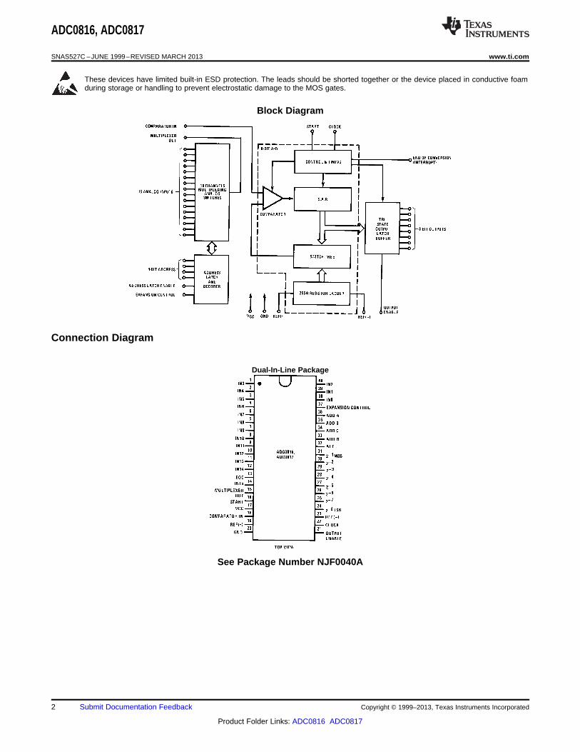
Block Diagram
Connection Diagram
Dual-In-Line Package
See Package Number NJF0040A
2 Submit Documentation Feedback Copyright © 1999–2013, Texas Instruments Incorporated
Product Folder Links: ADC0816 ADC0817
ADC0816, ADC0817
www.ti.com SNAS527C –JUNE 1999–REVISED MARCH 2013
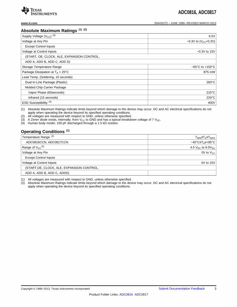
Absolute Maximum Ratings (1) (2)
Supply Voltage (VCC) (3) 6.5V
Voltage at Any Pin −0.3V to (VCC+0.3V)
Except Control Inputs
Voltage at Control Inputs −0.3V to 15V
(START, OE, CLOCK, ALE, EXPANSION CONTROL,
ADD A, ADD B, ADD C, ADD D)
Storage Temperature Range −65°C to +150°C
Package Dissipation at TA = 25°C 875 mW
Lead Temp. (Soldering, 10 seconds)
Dual-In-Line Package (Plastic) 260°C
Molded Chip Carrier Package
Vapor Phase (60seconds) 215°C
Infrared (15 seconds) 220°C
ESD Susceptibility (4) 400V
(1) Absolute Maximum Ratings indicate limits beyond which damage to the device may occur. DC and AC electrical specifications do notapply when operating the device beyond its specified operating conditions.
(2) All voltages are measured with respect to GND, unless otherwise specified.(3) A Zener diode exists, internally, from VCC to GND and has a typical breakdown voltage of 7 VDC.(4) Human body model, 100 pF discharged through a 1.5 kΩ resistor.
Operating Conditions (1)
Temperature Range (2) TMIN≤TA≤TMAX
ADC0816CCN, ADC0817CCN −40°C≤TA≤+85°C
Range of VCC(2) 4.5 VDC to 6.0VDC
Voltage at Any Pin 0V to VCC
Except Control Inputs
Voltage at Control Inputs 0V to 15V
(START,OE, CLOCK, ALE, EXPANSION CONTROL,
ADD A, ADD B, ADD C, ADDD)
(1) All voltages are measured with respect to GND, unless otherwise specified.(2) Absolute Maximum Ratings indicate limits beyond which damage to the device may occur. DC and AC electrical specifications do not
apply when operating the device beyond its specified operating conditions.
Copyright © 1999–2013, Texas Instruments Incorporated Submit Documentation Feedback 3
Product Folder Links: ADC0816 ADC0817
ADC0816, ADC0817
SNAS527C –JUNE 1999–REVISED MARCH 2013 www.ti.com
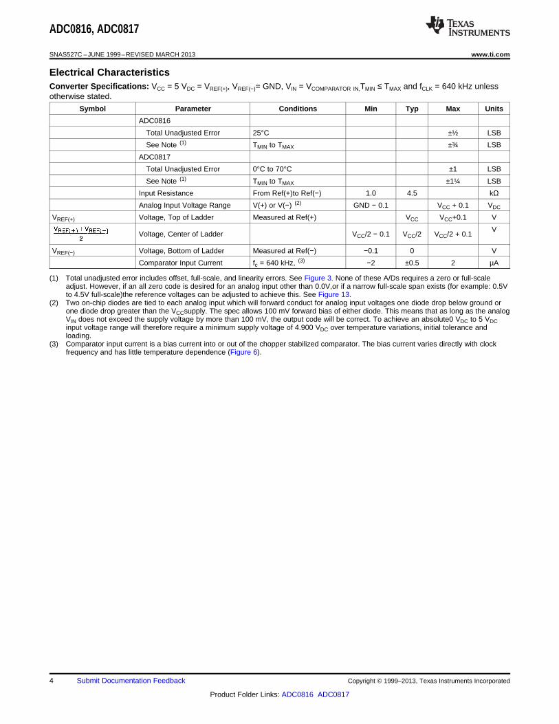
Electrical CharacteristicsConverter Specifications: VCC = 5 VDC = VREF(+), VREF(−)= GND, VIN = VCOMPARATOR IN,TMIN ≤ TMAX and fCLK = 640 kHz unlessotherwise stated.
Symbol Parameter Conditions Min Typ Max Units
ADC0816
Total Unadjusted Error 25°C ±½ LSB
See Note (1) TMIN to TMAX ±¾ LSB
ADC0817
Total Unadjusted Error 0°C to 70°C ±1 LSB
See Note (1) TMIN to TMAX ±1¼ LSB
Input Resistance From Ref(+)to Ref(−) 1.0 4.5 kΩAnalog Input Voltage Range V(+) or V(−) (2) GND − 0.1 VCC + 0.1 VDC
VREF(+) Voltage, Top of Ladder Measured at Ref(+) VCC VCC+0.1 V
VVoltage, Center of Ladder VCC/2 − 0.1 VCC/2 VCC/2 + 0.1
VREF(−) Voltage, Bottom of Ladder Measured at Ref(−) −0.1 0 V
Comparator Input Current fc = 640 kHz, (3) −2 ±0.5 2 µA
(1) Total unadjusted error includes offset, full-scale, and linearity errors. See Figure 3. None of these A/Ds requires a zero or full-scaleadjust. However, if an all zero code is desired for an analog input other than 0.0V,or if a narrow full-scale span exists (for example: 0.5Vto 4.5V full-scale)the reference voltages can be adjusted to achieve this. See Figure 13.
(2) Two on-chip diodes are tied to each analog input which will forward conduct for analog input voltages one diode drop below ground orone diode drop greater than the VCCsupply. The spec allows 100 mV forward bias of either diode. This means that as long as the analogVIN does not exceed the supply voltage by more than 100 mV, the output code will be correct. To achieve an absolute0 VDC to 5 VDCinput voltage range will therefore require a minimum supply voltage of 4.900 VDC over temperature variations, initial tolerance andloading.
(3) Comparator input current is a bias current into or out of the chopper stabilized comparator. The bias current varies directly with clockfrequency and has little temperature dependence (Figure 6).
4 Submit Documentation Feedback Copyright © 1999–2013, Texas Instruments Incorporated
Product Folder Links: ADC0816 ADC0817
ADC0816, ADC0817
www.ti.com SNAS527C –JUNE 1999–REVISED MARCH 2013
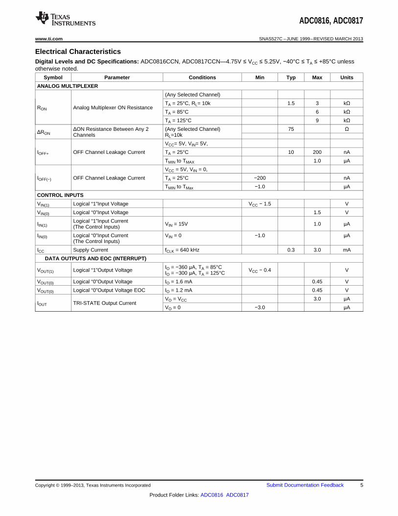
Electrical CharacteristicsDigital Levels and DC Specifications: ADC0816CCN, ADC0817CCN—4.75V ≤ VCC ≤ 5.25V, −40°C ≤ TA ≤ +85°C unlessotherwise noted.
Symbol Parameter Conditions Min Typ Max Units
ANALOG MULTIPLEXER
(Any Selected Channel)
TA = 25°C, RL= 10k 1.5 3 kΩRON Analog Multiplexer ON Resistance
TA = 85°C 6 kΩTA = 125°C 9 kΩ
ΔON Resistance Between Any 2 (Any Selected Channel) 75 ΩΔRON Channels RL=10k
VCC= 5V, VIN= 5V,
IOFF+ OFF Channel Leakage Current TA = 25°C 10 200 nA
TMIN to TMAX 1.0 μA
VCC = 5V, VIN = 0,
IOFF(−) OFF Channel Leakage Current TA = 25°C −200 nA
TMIN to TMax −1.0 μA
CONTROL INPUTS
VIN(1) Logical “1”Input Voltage VCC − 1.5 V
VIN(0) Logical “0”Input Voltage 1.5 V
Logical “1”Input CurrentIIN(1) VIN = 15V 1.0 μA(The Control Inputs)
IIN(0) Logical “0”Input Current VIN = 0 −1.0 μA(The Control Inputs)
ICC Supply Current fCLK = 640 kHz 0.3 3.0 mA
DATA OUTPUTS AND EOC (INTERRUPT)
IO = −360 μA, TA = 85°CVOUT(1) Logical “1”Output Voltage VCC − 0.4 VIO = −300 μA, TA = 125°C
VOUT(0) Logical “0”Output Voltage IO = 1.6 mA 0.45 V
VOUT(0) Logical “0”Output Voltage EOC IO = 1.2 mA 0.45 V
VO = VCC 3.0 μAIOUT TRI-STATE Output Current
VO = 0 −3.0 μA
Copyright © 1999–2013, Texas Instruments Incorporated Submit Documentation Feedback 5
Product Folder Links: ADC0816 ADC0817
ADC0816, ADC0817
SNAS527C –JUNE 1999–REVISED MARCH 2013 www.ti.com
Electrical CharacteristicsTiming Specifications:VCC = VREF(+) = 5V, VREF(−) = GND, tr = tf = 20 ns and TA = 25°C unless otherwise noted.
Symbol Parameter Conditions Min Typ Max Units
tWS Minimum Start Pulse Width (Figure 5) (1) 100 200 ns
tWALE Minimum ALE Pulse Width (Figure 5) 100 200 ns
ts Minimum Address Set-Up Time (Figure 5) 25 50 ns
TH Minimum Address Hold Time (Figure 5) 25 50 ns
Analog MUX Delay TimetD RS= OΩ (Figure 5) 1 2.5 μsfrom ALE
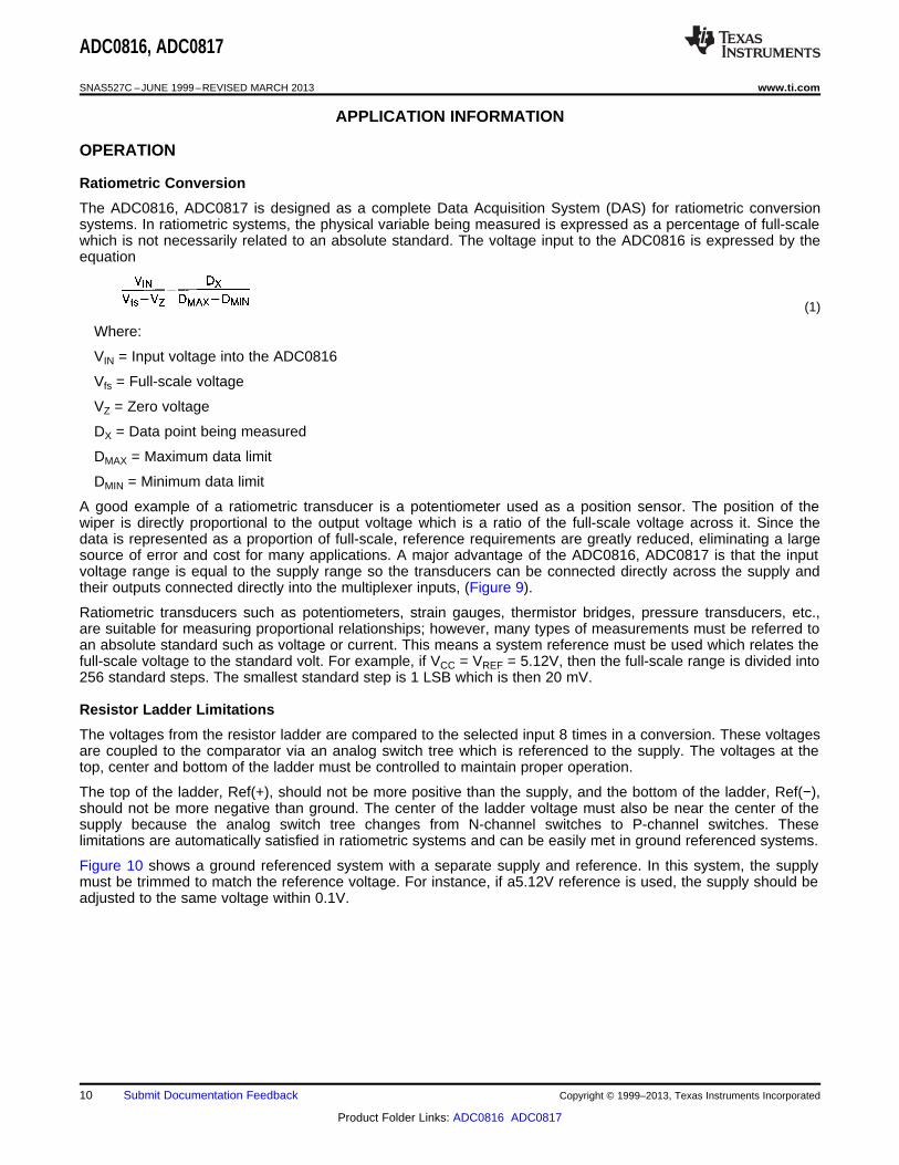
tH1, tH0 OE Control to Q Logic State CL= 50 pF, RL= 10k (Figure 8) 125 250 ns
t1H, t0H OE Control to Hi-Z CL= 10 pF, RL= 10k (Figure 8) 125 250 ns
tC Conversion Time fc=640 kHz, (Figure 5) (2) 90 100 116 μs
fc Clock Frequency 10 640 1280 kHz
ClocktEOC EOC Delay Time (Figure 5) 0 8 + 2μs Periods
CIN Input Capacitance At Control Inputs 10 15 pF
TRI-STATE OutputCOUT At TRI-STATE Outputs (2) 10 15 pFCapacitance
(1) If start pulse is asynchronous with converter clock or if fc > 640 kHz, the minimum start pulse width is 8clock periods plus 2 μs. Forsynchronous operation at fc ≤640 kHz take start high within 100 ns of clock going low.
(2) The outputs of the data register are updated one clock cycle before the rising edge of EOC.
Functional Description
Multiplexer: The device contains a 16-channel single-ended analog signal multiplexer. A particular input channelis selected by using the address decoder. Table 1 shows the input states for the address line and the expansioncontrol line to select any channel. The address is latched into the decoder on the low-to-high transition of theaddress latch enable signal.
Table 1. Inputs States for the Address line
Selected Address Line (1) Expansion
AnalogChannel D C B A Control
IN0 L L L L H
IN1 L L L H H
IN2 L L H L H
IN3 L L H H H
IN4 L H L L H
IN5 L H L H H
IN6 L H H L H
IN7 L H H H H
IN8 H L L L H
IN9 H L L H H
IN10 H L H L H
IN11 H L H H H
IN12 H H L L H
IN13 H H L H H
IN14 H H H L H
IN15 H H H H H
All Channels OFF X X X X L
(1) X = don't care
6 Submit Documentation Feedback Copyright © 1999–2013, Texas Instruments Incorporated
Product Folder Links: ADC0816 ADC0817
ADC0816, ADC0817
www.ti.com SNAS527C –JUNE 1999–REVISED MARCH 2013
Additional single-ended analog signals can be multiplexed to the A/D converter by disabling all the multiplexerinputs using the expansion control. The additional external signals are connected to the comparator input and thedevice ground. Additional signal conditioning (i.e., prescaling, sample and hold, instrumentation amplification,etc.) may also be added between the analog input signal and the comparator input.
CONVERTER CHARACTERISTICS
The Converter
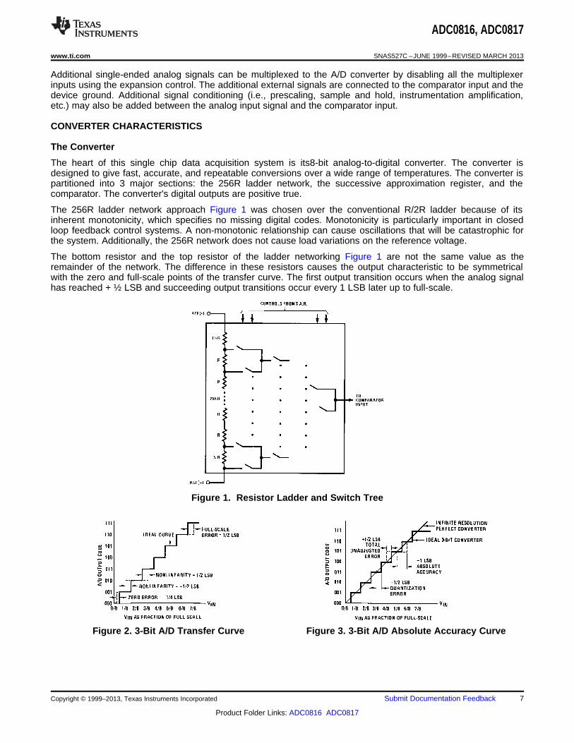
The heart of this single chip data acquisition system is its8-bit analog-to-digital converter. The converter isdesigned to give fast, accurate, and repeatable conversions over a wide range of temperatures. The converter ispartitioned into 3 major sections: the 256R ladder network, the successive approximation register, and thecomparator. The converter's digital outputs are positive true.
The 256R ladder network approach Figure 1 was chosen over the conventional R/2R ladder because of itsinherent monotonicity, which specifies no missing digital codes. Monotonicity is particularly important in closedloop feedback control systems. A non-monotonic relationship can cause oscillations that will be catastrophic forthe system. Additionally, the 256R network does not cause load variations on the reference voltage.
The bottom resistor and the top resistor of the ladder networking Figure 1 are not the same value as theremainder of the network. The difference in these resistors causes the output characteristic to be symmetricalwith the zero and full-scale points of the transfer curve. The first output transition occurs when the analog signalhas reached + ½ LSB and succeeding output transitions occur every 1 LSB later up to full-scale.
Figure 1. Resistor Ladder and Switch Tree
Figure 2. 3-Bit A/D Transfer Curve Figure 3. 3-Bit A/D Absolute Accuracy Curve
Copyright © 1999–2013, Texas Instruments Incorporated Submit Documentation Feedback 7
Product Folder Links: ADC0816 ADC0817
ADC0816, ADC0817
SNAS527C –JUNE 1999–REVISED MARCH 2013 www.ti.com
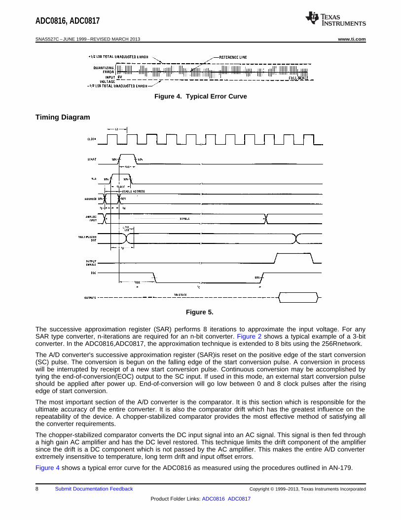
Figure 4. Typical Error Curve
Timing Diagram
Figure 5.
The successive approximation register (SAR) performs 8 iterations to approximate the input voltage. For anySAR type converter, n-iterations are required for an n-bit converter. Figure 2 shows a typical example of a 3-bitconverter. In the ADC0816,ADC0817, the approximation technique is extended to 8 bits using the 256Rnetwork.
The A/D converter's successive approximation register (SAR)is reset on the positive edge of the start conversion(SC) pulse. The conversion is begun on the falling edge of the start conversion pulse. A conversion in processwill be interrupted by receipt of a new start conversion pulse. Continuous conversion may be accomplished bytying the end-of-conversion(EOC) output to the SC input. If used in this mode, an external start conversion pulseshould be applied after power up. End-of-conversion will go low between 0 and 8 clock pulses after the risingedge of start conversion.
The most important section of the A/D converter is the comparator. It is this section which is responsible for theultimate accuracy of the entire converter. It is also the comparator drift which has the greatest influence on therepeatability of the device. A chopper-stabilized comparator provides the most effective method of satisfying allthe converter requirements.
The chopper-stabilized comparator converts the DC input signal into an AC signal. This signal is then fed througha high gain AC amplifier and has the DC level restored. This technique limits the drift component of the amplifiersince the drift is a DC component which is not passed by the AC amplifier. This makes the entire A/D converterextremely insensitive to temperature, long term drift and input offset errors.
Figure 4 shows a typical error curve for the ADC0816 as measured using the procedures outlined in AN-179.
8 Submit Documentation Feedback Copyright © 1999–2013, Texas Instruments Incorporated
Product Folder Links: ADC0816 ADC0817
ADC0816, ADC0817
www.ti.com SNAS527C –JUNE 1999–REVISED MARCH 2013
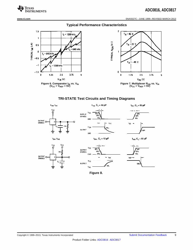
Typical Performance Characteristics
Figure 6. Comparator IIN vs. VIN Figure 7. Multiplexer RON vs. VIN(VCC = VREF = 5V) (VCC = VREF = 5V)
spacerTRI-STATE Test Circuits and Timing Diagrams
Figure 8.
Copyright © 1999–2013, Texas Instruments Incorporated Submit Documentation Feedback 9
Product Folder Links: ADC0816 ADC0817
ADC0816, ADC0817
SNAS527C –JUNE 1999–REVISED MARCH 2013 www.ti.com
APPLICATION INFORMATION
OPERATION
Ratiometric Conversion
The ADC0816, ADC0817 is designed as a complete Data Acquisition System (DAS) for ratiometric conversionsystems. In ratiometric systems, the physical variable being measured is expressed as a percentage of full-scalewhich is not necessarily related to an absolute standard. The voltage input to the ADC0816 is expressed by theequation
(1)
Where:
VIN = Input voltage into the ADC0816
Vfs = Full-scale voltage
VZ = Zero voltage
DX = Data point being measured
DMAX = Maximum data limit
DMIN = Minimum data limit
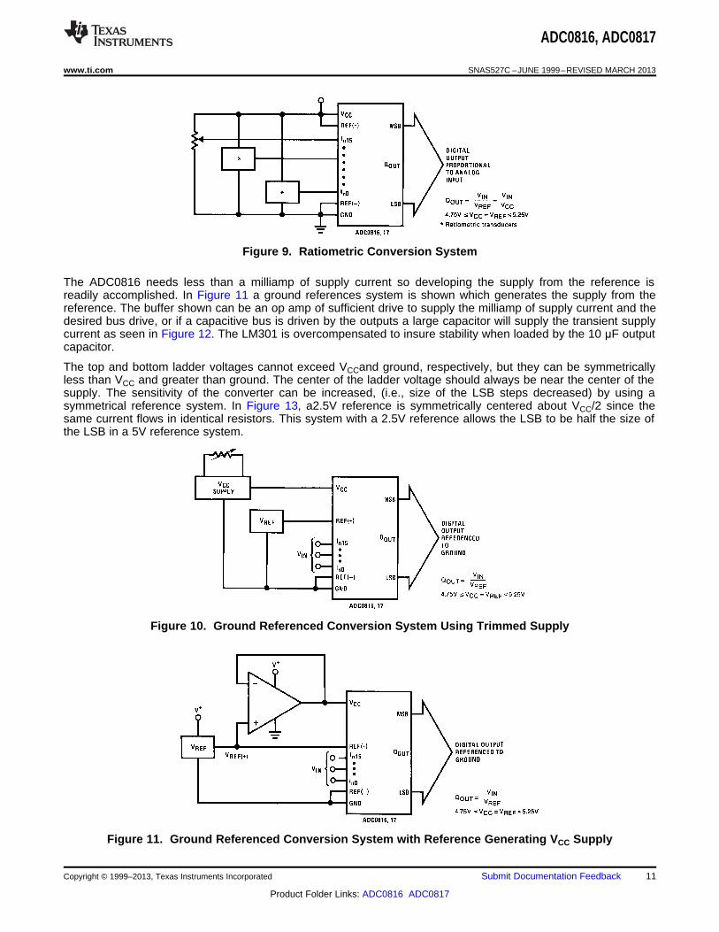
A good example of a ratiometric transducer is a potentiometer used as a position sensor. The position of thewiper is directly proportional to the output voltage which is a ratio of the full-scale voltage across it. Since thedata is represented as a proportion of full-scale, reference requirements are greatly reduced, eliminating a largesource of error and cost for many applications. A major advantage of the ADC0816, ADC0817 is that the inputvoltage range is equal to the supply range so the transducers can be connected directly across the supply andtheir outputs connected directly into the multiplexer inputs, (Figure 9).
Ratiometric transducers such as potentiometers, strain gauges, thermistor bridges, pressure transducers, etc.,are suitable for measuring proportional relationships; however, many types of measurements must be referred toan absolute standard such as voltage or current. This means a system reference must be used which relates thefull-scale voltage to the standard volt. For example, if VCC = VREF = 5.12V, then the full-scale range is divided into256 standard steps. The smallest standard step is 1 LSB which is then 20 mV.
Resistor Ladder Limitations
The voltages from the resistor ladder are compared to the selected input 8 times in a conversion. These voltagesare coupled to the comparator via an analog switch tree which is referenced to the supply. The voltages at thetop, center and bottom of the ladder must be controlled to maintain proper operation.
The top of the ladder, Ref(+), should not be more positive than the supply, and the bottom of the ladder, Ref(−),should not be more negative than ground. The center of the ladder voltage must also be near the center of thesupply because the analog switch tree changes from N-channel switches to P-channel switches. Theselimitations are automatically satisfied in ratiometric systems and can be easily met in ground referenced systems.
Figure 10 shows a ground referenced system with a separate supply and reference. In this system, the supplymust be trimmed to match the reference voltage. For instance, if a5.12V reference is used, the supply should beadjusted to the same voltage within 0.1V.
10 Submit Documentation Feedback Copyright © 1999–2013, Texas Instruments Incorporated
Product Folder Links: ADC0816 ADC0817
ADC0816, ADC0817
www.ti.com SNAS527C –JUNE 1999–REVISED MARCH 2013
Figure 9. Ratiometric Conversion System
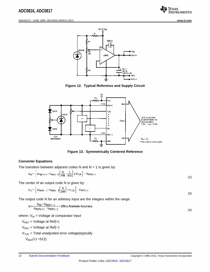
The ADC0816 needs less than a milliamp of supply current so developing the supply from the reference isreadily accomplished. In Figure 11 a ground references system is shown which generates the supply from thereference. The buffer shown can be an op amp of sufficient drive to supply the milliamp of supply current and thedesired bus drive, or if a capacitive bus is driven by the outputs a large capacitor will supply the transient supplycurrent as seen in Figure 12. The LM301 is overcompensated to insure stability when loaded by the 10 μF outputcapacitor.
The top and bottom ladder voltages cannot exceed VCCand ground, respectively, but they can be symmetricallyless than VCC and greater than ground. The center of the ladder voltage should always be near the center of thesupply. The sensitivity of the converter can be increased, (i.e., size of the LSB steps decreased) by using asymmetrical reference system. In Figure 13, a2.5V reference is symmetrically centered about VCC/2 since thesame current flows in identical resistors. This system with a 2.5V reference allows the LSB to be half the size ofthe LSB in a 5V reference system.
Figure 10. Ground Referenced Conversion System Using Trimmed Supply
Figure 11. Ground Referenced Conversion System with Reference Generating VCC Supply
Copyright © 1999–2013, Texas Instruments Incorporated Submit Documentation Feedback 11
Product Folder Links: ADC0816 ADC0817
ADC0816, ADC0817
SNAS527C –JUNE 1999–REVISED MARCH 2013 www.ti.com
Figure 12. Typical Reference and Supply Circuit
Figure 13. Symmetrically Centered Reference
Converter Equations
The transition between adjacent codes N and N + 1 is given by:
(2)
The center of an output code N is given by:
(3)
The output code N for an arbitrary input are the integers within the range:
(4)
where: VIN = Voltage at comparator input
VREF = Voltage at Ref(+)
VREF = Voltage at Ref(−)
VTUE = Total unadjusted error voltage(typically
VREF(+) ÷512)
12 Submit Documentation Feedback Copyright © 1999–2013, Texas Instruments Incorporated
Product Folder Links: ADC0816 ADC0817
ADC0816, ADC0817
www.ti.com SNAS527C –JUNE 1999–REVISED MARCH 2013
Analog Comparator Inputs
The dynamic comparator input current is caused by the periodic switching of on-chip stray capacitances Theseare connected alternately to the output of the resistor ladder/switch tree network and to the comparator input aspart of the operation of the chopper stabilized comparator.
The average value of the comparator input current varies directly with clock frequency and with VIN as shown inFigure 6.
If no filter capacitors are used at the analog or comparator inputs and the signal source impedances are low, thecomparator input current should not introduce converter errors, as the transient created by the capacitancedischarge will die out before the comparator output is strobed.
If input filter capacitors are desired for noise reduction and signal conditioning they will tend to average out thedynamic comparator input current. It will then take on the characteristics of a DC bias current whose effect canbe predicted conventionally. See AN-258 for further discussion.
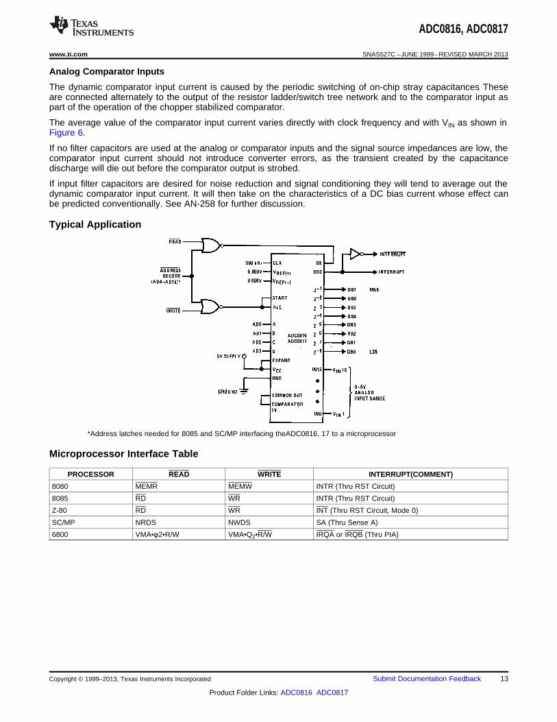
Typical Application
*Address latches needed for 8085 and SC/MP interfacing theADC0816, 17 to a microprocessor
Microprocessor Interface Table
PROCESSOR READ WRITE INTERRUPT(COMMENT)
8080 MEMR MEMW INTR (Thru RST Circuit)
8085 RD WR INTR (Thru RST Circuit)
Z-80 RD WR INT (Thru RST Circuit, Mode 0)
SC/MP NRDS NWDS SA (Thru Sense A)
6800 VMA•φ2•R/W VMA•Q2•R/W IRQA or IRQB (Thru PIA)
Copyright © 1999–2013, Texas Instruments Incorporated Submit Documentation Feedback 13
Product Folder Links: ADC0816 ADC0817
ADC0816, ADC0817
SNAS527C –JUNE 1999–REVISED MARCH 2013 www.ti.com
REVISION HISTORY
Changes from Revision B (March 2013) to Revision C Page
• Changed layout of National Data Sheet to TI format .......................................................................................................... 13
14 Submit Documentation Feedback Copyright © 1999–2013, Texas Instruments Incorporated
Product Folder Links: ADC0816 ADC0817
PACKAGE OPTION ADDENDUM
www.ti.com 12-Jul-2014
Addendum-Page 1
PACKAGING INFORMATION
Orderable Device Status(1)
Package Type PackageDrawing
Pins PackageQty
Eco Plan(2)
Lead/Ball Finish(6)
MSL Peak Temp(3)
Op Temp (°C) Device Marking(4/5)
Samples
ADC0816CCN NRND PDIP NFJ 40 9 TBD Call TI Call TI -40 to 85 ADC0816CCN
ADC0816CCN/NOPB ACTIVE PDIP NFJ 40 9 Green (RoHS& no Sb/Br)
CU SN Level-1-NA-UNLIM -40 to 85 ADC0816CCN
ADC0817CCN NRND PDIP NFJ 40 9 TBD Call TI Call TI -40 to 85 ADC0817CCN
ADC0817CCN/NOPB ACTIVE PDIP NFJ 40 9 Green (RoHS& no Sb/Br)
CU SN Level-1-NA-UNLIM -40 to 85 ADC0817CCN
(1) The marketing status values are defined as follows:ACTIVE: Product device recommended for new designs.LIFEBUY: TI has announced that the device will be discontinued, and a lifetime-buy period is in effect.NRND: Not recommended for new designs. Device is in production to support existing customers, but TI does not recommend using this part in a new design.PREVIEW: Device has been announced but is not in production. Samples may or may not be available.OBSOLETE: TI has discontinued the production of the device.
(2) Eco Plan - The planned eco-friendly classification: Pb-Free (RoHS), Pb-Free (RoHS Exempt), or Green (RoHS & no Sb/Br) - please check http://www.ti.com/productcontent for the latest availabilityinformation and additional product content details.TBD: The Pb-Free/Green conversion plan has not been defined.Pb-Free (RoHS): TI's terms "Lead-Free" or "Pb-Free" mean semiconductor products that are compatible with the current RoHS requirements for all 6 substances, including the requirement thatlead not exceed 0.1% by weight in homogeneous materials. Where designed to be soldered at high temperatures, TI Pb-Free products are suitable for use in specified lead-free processes.Pb-Free (RoHS Exempt): This component has a RoHS exemption for either 1) lead-based flip-chip solder bumps used between the die and package, or 2) lead-based die adhesive used betweenthe die and leadframe. The component is otherwise considered Pb-Free (RoHS compatible) as defined above.Green (RoHS & no Sb/Br): TI defines "Green" to mean Pb-Free (RoHS compatible), and free of Bromine (Br) and Antimony (Sb) based flame retardants (Br or Sb do not exceed 0.1% by weightin homogeneous material)
(3) MSL, Peak Temp. - The Moisture Sensitivity Level rating according to the JEDEC industry standard classifications, and peak solder temperature.
(4) There may be additional marking, which relates to the logo, the lot trace code information, or the environmental category on the device.
(5) Multiple Device Markings will be inside parentheses. Only one Device Marking contained in parentheses and separated by a "~" will appear on a device. If a line is indented then it is a continuationof the previous line and the two combined represent the entire Device Marking for that device.
(6) Lead/Ball Finish - Orderable Devices may have multiple material finish options. Finish options are separated by a vertical ruled line. Lead/Ball Finish values may wrap to two lines if the finishvalue exceeds the maximum column width.
Important Information and Disclaimer:The information provided on this page represents TI's knowledge and belief as of the date that it is provided. TI bases its knowledge and belief on informationprovided by third parties, and makes no representation or warranty as to the accuracy of such information. Efforts are underway to better integrate information from third parties. TI has taken and
PACKAGE OPTION ADDENDUM
www.ti.com 12-Jul-2014
Addendum-Page 2
continues to take reasonable steps to provide representative and accurate information but may not have conducted destructive testing or chemical analysis on incoming materials and chemicals.TI and TI suppliers consider certain information to be proprietary, and thus CAS numbers and other limited information may not be available for release.
In no event shall TI's liability arising out of such information exceed the total purchase price of the TI part(s) at issue in this document sold by TI to Customer on an annual basis.
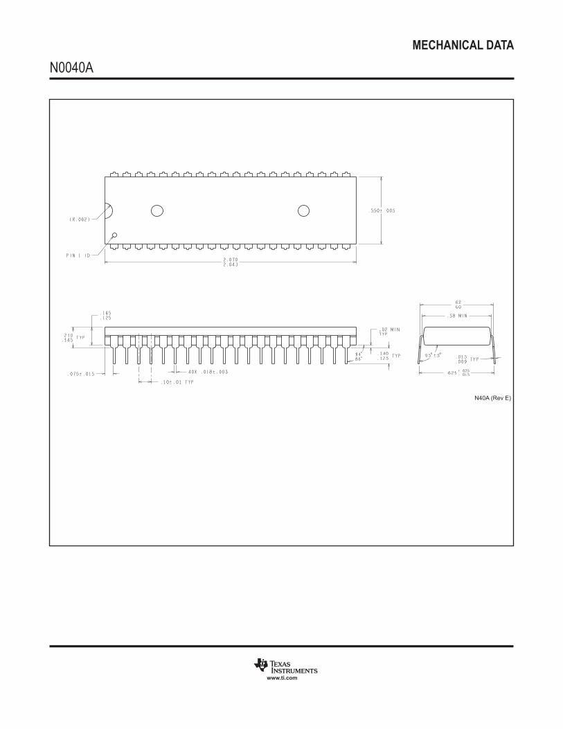
MECHANICAL DATA
N0040A
www.ti.com
N40A (Rev E)

IMPORTANT NOTICETexas Instruments Incorporated and its subsidiaries (TI) reserve the right to make corrections, enhancements, improvements and otherchanges to its semiconductor products and services per JESD46, latest issue, and to discontinue any product or service per JESD48, latestissue. Buyers should obtain the latest relevant information before placing orders and should verify that such information is current andcomplete. All semiconductor products (also referred to herein as “components”) are sold subject to TI’s terms and conditions of salesupplied at the time of order acknowledgment.TI warrants performance of its components to the specifications applicable at the time of sale, in accordance with the warranty in TI’s termsand conditions of sale of semiconductor products. Testing and other quality control techniques are used to the extent TI deems necessaryto support this warranty. Except where mandated by applicable law, testing of all parameters of each component is not necessarilyperformed.TI assumes no liability for applications assistance or the design of Buyers’ products. Buyers are responsible for their products andapplications using TI components. To minimize the risks associated with Buyers’ products and applications, Buyers should provideadequate design and operating safeguards.TI does not warrant or represent that any license, either express or implied, is granted under any patent right, copyright, mask work right, orother intellectual property right relating to any combination, machine, or process in which TI components or services are used. Informationpublished by TI regarding third-party products or services does not constitute a license to use such products or services or a warranty orendorsement thereof. Use of such information may require a license from a third party under the patents or other intellectual property of thethird party, or a license from TI under the patents or other intellectual property of TI.Reproduction of significant portions of TI information in TI data books or data sheets is permissible only if reproduction is without alterationand is accompanied by all associated warranties, conditions, limitations, and notices. TI is not responsible or liable for such altereddocumentation. Information of third parties may be subject to additional restrictions.Resale of TI components or services with statements different from or beyond the parameters stated by TI for that component or servicevoids all express and any implied warranties for the associated TI component or service and is an unfair and deceptive business practice.TI is not responsible or liable for any such statements.Buyer acknowledges and agrees that it is solely responsible for compliance with all legal, regulatory and safety-related requirementsconcerning its products, and any use of TI components in its applications, notwithstanding any applications-related information or supportthat may be provided by TI. Buyer represents and agrees that it has all the necessary expertise to create and implement safeguards whichanticipate dangerous consequences of failures, monitor failures and their consequences, lessen the likelihood of failures that might causeharm and take appropriate remedial actions. Buyer will fully indemnify TI and its representatives against any damages arising out of the useof any TI components in safety-critical applications.In some cases, TI components may be promoted specifically to facilitate safety-related applications. With such components, TI’s goal is tohelp enable customers to design and create their own end-product solutions that meet applicable functional safety standards andrequirements. Nonetheless, such components are subject to these terms.No TI components are authorized for use in FDA Class III (or similar life-critical medical equipment) unless authorized officers of the partieshave executed a special agreement specifically governing such use.Only those TI components which TI has specifically designated as military grade or “enhanced plastic” are designed and intended for use inmilitary/aerospace applications or environments. Buyer acknowledges and agrees that any military or aerospace use of TI componentswhich have not been so designated is solely at the Buyer's risk, and that Buyer is solely responsible for compliance with all legal andregulatory requirements in connection with such use.TI has specifically designated certain components as meeting ISO/TS16949 requirements, mainly for automotive use. In any case of use ofnon-designated products, TI will not be responsible for any failure to meet ISO/TS16949.Products ApplicationsAudio www.ti.com/audio Automotive and Transportation www.ti.com/automotiveAmplifiers amplifier.ti.com Communications and Telecom www.ti.com/communicationsData Converters dataconverter.ti.com Computers and Peripherals www.ti.com/computersDLP® Products www.dlp.com Consumer Electronics www.ti.com/consumer-appsDSP dsp.ti.com Energy and Lighting www.ti.com/energyClocks and Timers www.ti.com/clocks Industrial www.ti.com/industrialInterface interface.ti.com Medical www.ti.com/medicalLogic logic.ti.com Security www.ti.com/securityPower Mgmt power.ti.com Space, Avionics and Defense www.ti.com/space-avionics-defenseMicrocontrollers microcontroller.ti.com Video and Imaging www.ti.com/videoRFID www.ti-rfid.comOMAP Applications Processors www.ti.com/omap TI E2E Community e2e.ti.comWireless Connectivity www.ti.com/wirelessconnectivity
Mailing Address: Texas Instruments, Post Office Box 655303, Dallas, Texas 75265Copyright © 2014, Texas Instruments Incorporated