additive growth and crystallization of polymer filmsspikelab/papers/127.pdf · additive growth and...
TRANSCRIPT

Additive Growth and Crystallization of Polymer FilmsHyuncheol Jeong,† Kimberly B. Shepard,† Geoffrey E. Purdum,† Yunlong Guo,†,§ Yueh-Lin Loo,†,‡
Craig B. Arnold,‡,⊥ and Rodney D. Priestley*,†,‡
†Department of Chemical and Biological Engineering, Princeton University, Princeton, New Jersey 08544 United States‡Princeton Institute for the Science and Technology of Materials, Princeton University, Princeton, New Jersey 08544 United States⊥Mechanical and Aerospace Engineering, Princeton University, Princeton, New Jersey 08544 United States
*S Supporting Information
ABSTRACT: We demonstrated a polymeric thin filmfabrication process in which molecular-scale crystallizationproceeds with additive film growth, by employing aninnovative vapor-assisted deposition process termed matrix-assisted pulsed laser evaporation (MAPLE). In comparison tosolution-casting commonly adopted for the deposition ofpolymer thin films, this physical vapor deposition (PVD)methodology can prolong the time scale of film formation andallow for the manipulation of temperature during deposition.For the deposition of molecular and atomic systems, such aPVD manner has been demonstrated to facilitate molecularordering and delicately manipulate crystalline morphologyduring film growth. Here, using MAPLE, we deposited thinfilms of a model polymer, poly(ethylene oxide) (PEO), atop a temperature-controlled substrate with an average growth rate ofless than 10 nm/h. The mechanism of deposition is sequential addition of nanoscale liquid droplets. We discovered that thedeposition process leads to the formation of two-dimensional (2D) PEO crystals, composed of monolamellar crystals laterallygrown from larger nucleus droplets. The 2D crystalline coverage and crystal thickness of the films can be manipulated with twoprocessing parameters, deposition time, and temperature.
■ INTRODUCTION
Semicrystalline polymer thin films have been extensivelyinvestigated as an enabling material for many technologies,including advanced barrier coatings,1 pressure/imaging sen-sors,2,3 electronic memories,4,5 and energy devices.6,7 In allapplications, control of the crystalline morphology is ofparamount importance due to the observed correlationsbetween structure and performance.1,4,6,7 Typically, polymerthin films are prepared by casting from solution. However,while deposition is facile and economically appealing, the shortprocessing time combined with rapid vitrification limitsmorphological development of the crystalline domains inpolymer thin films.7−9 To circumvent this issue, efforts tocontrol and improve crystalline morphology in polymer thinfilms, e.g., active layers in organic electronics, have aimed toprolong the time scale of vitrification or enhance molecularmobility during or subsequent to film deposition.8−12 Thesuccess of these strategies suggests that it would be beneficial tohave a processing route in which slow film growth andcrystallization can occur simultaneously.Recently, there has been a considerable effort to exploit the
unique advantages of matrix assisted pulsed laser evaporation(MAPLE) for the growth of polymer thin films.13−16 In theMAPLE process, a pulsed laser ablates a target consisting of afrozen dilute solution of the desired polymer. The frozen matrix
solution serves as a sacrificial matrix to transport the polymerinto the gas phase. Contrary to direct laser ablation, MAPLEprovides a gentle and nondestructive means for polymer filmdeposition.14 Control of various process parameters has beenshown to tune film morphology. For instance, MAPLE hasbeen shown to control preferential crystal orientation and theextent of crystallinity in thin polymer films by adjusting thematrix formulation17 and substrate temperature,18 respectively.Conceptually, the film growth in MAPLE proceeds by the
additive deposition of nanometer-sized droplets comprising thetarget polymer.20,21 With tunable laser pulse rates and targetpolymer concentration, the average film growth ratesthroughout the substrate can be controlled to <1 nm/s, thusenabling the slow growth of polymer films in a manner recentlyadvocated for organic electronics.19 There are some exper-imental and simulation reports that investigated the nature ofablation process in MAPLE22,23 and the size distribution ofpolymer droplets as a function of process parameters.21,24 Howthe mechanism of MAPLE, i.e., the deposition of nanoscalepolymer droplets, influences the morphology of semicrystallinepolymer films has not been investigated. We note that this
Received: December 10, 2015Revised: March 8, 2016Published: March 22, 2016
Article
pubs.acs.org/Macromolecules
© 2016 American Chemical Society 2860 DOI: 10.1021/acs.macromol.5b02675Macromolecules 2016, 49, 2860−2867
effect could be significant, as nanoscale confinement stronglyinfluences polymer crystallization.1,25−32 To achieve such astudy requires ultraslow MAPLE deposition to allow for thecapture of the early stages of film growth and crystallinemorphology.Here, we employ atomic force microscopy (AFM) to
investigate the early stages of film growth and crystallizationof a semicrystalline polymer film deposited by MAPLE at slowgrowth rates. The study is undertaken using poly(ethyleneoxide) (PEO), a model polymer, in which crystallization inthin-film geometry has been thoroughly investigated.1,25−29,33
The average film growth rate was extremely slow, ∼6 nm/h, topromote the simultaneous occurrence of film formation andcrystallization. We investigated the influence of growth timeand deposition temperature on the crystalline film morphologyof PEO deposited atop as-received silicon wafers (AR-Si). Wefound that the film morphology strongly depends on theseprocess parameters. We anticipate that our findings will informthe future use of MAPLE as a processing tool to deposit thinfilms of semicrystalline polymers in which control of themorphology is desired.
■ RESULTS AND DISCUSSION
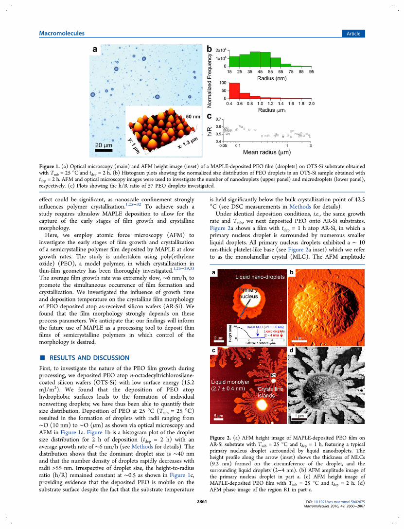
First, to investigate the nature of the PEO film growth duringprocessing, we deposited PEO atop n-octadecyltrichlorosilane-coated silicon wafers (OTS-Si) with low surface energy (15.2mJ/m2). We found that the deposition of PEO atophydrophobic surfaces leads to the formation of individualnonwetting droplets; we have thus been able to quantify theirsize distribution. Deposition of PEO at 25 °C (Tsub = 25 °C)resulted in the formation of droplets with radii ranging from∼O (10 nm) to ∼O (μm) as shown via optical microscopy andAFM in Figure 1a. Figure 1b is a histogram plot of the dropletsize distribution for 2 h of deposition (tdep = 2 h) with anaverage growth rate of ∼6 nm/h (see Methods for details). Thedistribution shows that the dominant droplet size is ∼40 nmand that the number density of droplets rapidly decreases withradii >55 nm. Irrespective of droplet size, the height-to-radiusratio (h/R) remained constant at ∼0.5 as shown in Figure 1c,providing evidence that the deposited PEO is mobile on thesubstrate surface despite the fact that the substrate temperature
is held significantly below the bulk crystallization point of 42.5°C (see DSC measurements in Methods for details).Under identical deposition conditions, i.e., the same growth
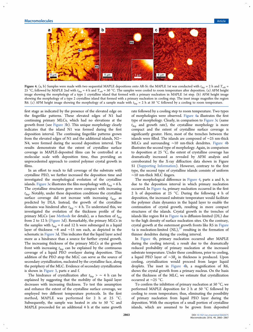
rate and Tsub, we next deposited PEO onto AR-Si substrates.Figure 2a shows a film with tdep = 1 h atop AR-Si, in which aprimary nucleus droplet is surrounded by numerous smallerliquid droplets. All primary nucleus droplets exhibited a ∼ 10nm-thick platelet-like base (see Figure 2a inset) which we referto as the monolamellar crystal (MLC). The AFM amplitude
Figure 1. (a) Optical microscopy (main) and AFM height image (inset) of a MAPLE-deposited PEO film (droplets) on OTS-Si substrate obtainedwith Tsub = 25 °C and tdep = 2 h. (b) Histogram plots showing the normalized size distribution of PEO droplets in an OTS-Si sample obtained withtdep = 2 h. AFM and optical microscopy images were used to investigate the number of nanodroplets (upper panel) and microdroplets (lower panel),respectively. (c) Plots showing the h/R ratio of 57 PEO droplets investigated.
Figure 2. (a) AFM height image of MAPLE-deposited PEO film onAR-Si substrate with Tsub = 25 °C and tdep = 1 h, featuring a typicalprimary nucleus droplet surrounded by liquid nanodroplets. Theheight profile along the arrow (inset) shows the thickness of MLCs(9.2 nm) formed on the circumference of the droplet, and thesurrounding liquid droplets (2−4 nm). (b) AFM amplitude image ofthe primary nucleus droplet in part a. (c) AFM height image ofMAPLE-deposited PEO film with Tsub = 25 °C and tdep = 2 h. (d)AFM phase image of the region R1 in part c.
Macromolecules Article
DOI: 10.1021/acs.macromol.5b02675Macromolecules 2016, 49, 2860−2867
2861

error image of a primary nucleus droplet (Figure 2b) reveals aspiral-growth morphology. Furthermore, the conformation ofliquid droplets atop AR-Si differed from those atop OTS-Si.The liquid droplets observed in Figure 2a were 2−4 nm inheight irrespective of their lateral size. This height iscomparable to the Rg of PEO with Mn = 4600 g/mol,suggesting that the liquid droplets on AR-Si were composed ofa monolayer of PEO due to attractive interactions with thesubstrate.34
When increasing tdep to 2 h, the primary nuclei developedmore pronounced fingerlike crystal patterns as shown in theFigure 2c. Grown from the base of the primary nuclei, thefingerlike MLCs exhibited a thickness of ∼10 nm. The liquidregions surrounding the crystalline islands also transformedfrom an ensemble of discrete droplets to a continuous film, thusforming a monolayer-thick (2.7 ± 0.4 nm) liquid layer. Figure2d shows the AFM phase image of region R1 in Figure 2c. Thespiral morphology of the primary nucleus, the finger-like MLCs,as well as the liquid monolayer are all clearly depicted. Inaddition, liquid droplets were observed on the surface of theMLCs.The unique film morphology on AR-Si is a consequence of
the deposition mechanism, that is, the additive assembly of asize-distribution of liquid nanodroplets. Smaller droplets areunable to crystallize by themselves due to low nucleationprobability;26 instead, they adsorb to the substrate to form aliquid layer. In contrast, larger droplets undergo crystalliza-
tion27 when deposit onto low-temperature substrates, which wedenote as primary nucleation. Henceforth, crystal growth of thefingerlike primary MLCs proceeds from the primary nucleialong the substrate, facilitated by the presence of the nearbyliquid layer. Unlike crystallization of spin-cast films, in whichmolecular ordering is achieved during rapid solidification of theentire film, here molecular ordering is achieved withinnanoconfined regions over the long time scales of film growth.The fingerlike morphology is due to the limited diffusion ofPEO to the crystal growth front at large undercoolings, aspredicted by the diffusion-limited aggregation (DLA)model.27,35
Film growth in which molecular-scale crystallization occursprior to the deposition of more material provides a uniquemeans to tune crystal nucleation and growth, hence giving theresulting morphology, as previously demonstrated for metallicor molecular films36,37 To investigate the relationship betweentdep and the extent of crystalline surface coverage, we conductedtwo sequential MAPLE depositions with 2 h intervals on thesame AR-Si substrate at 25 °C with an intervening thermalannealing step at 35 °C for 3 h after the first 2 h depositioninterval. The film morphology is illustrated in Figure 3a.Thickening of crystal boundaries occurs during thermalannealing,28,33 and therefore, can serve as a marker indistinguishing crystals formed in the first from the secondMAPLE deposition. Among the four crystalline islands,denoted N1−N4 in Figure 3a, only N1 was deposited in the
Figure 3. (a) AFM height image showing the film morphology formed on AR-Si substrate with two sequential MAPLE depositions (first and secondMAPLE) of tdep = 2 h at 25 °C respectively, with an intervening thermal annealing at 35 °C for 3 h in atmosphere. (b) AFM height image of theregion R2 in part a. The height profile along the arrow (lower panel) shows the thermally induced elevation in the middle of the MLC that clearlydistinguishes the MLC formed on MAPLE second deposition (blue) from the MLC formed on MAPLE first (red). (c) AFM height image ofMAPLE-deposited film with tdep = 6 h (d) Schematic showing the film structure in part c (upper panel) and plots showing the evolution of heightprofiles of films with tdep (2, 6, and 12 h) (lower panel). Primary MLCs and liquid layers are shown with dotted and solid lines, respectively. (e) AFMheight image showing the secondary crystals formed on the partially submerged periphery of crystalline islands. (f) AFM height image of the regionR3 in part e. The height profile along the arrow (lower panel) shows the secondary crystals (blue).
Macromolecules Article
DOI: 10.1021/acs.macromol.5b02675Macromolecules 2016, 49, 2860−2867
2862
first stage as indicated by the presence of the elevated edge onthe fingerlike patterns. These elevated edges of N1 hadcontinuing primary MLCs, which had no elevations at thegrowth front (see Figure 3b). This unique morphology clearlyindicates that the island N1 was formed during the firstdeposition interval. The continuing fingerlike patterns grownfrom the elevated edges of N1 and the additional islands, N2−N4, were formed during the second deposition interval. Theresults demonstrate that the extent of crystalline surfacecoverage in MAPLE-deposited films can be controlled at amolecular scale with deposition time, thus providing anunprecedented approach to control polymer crystal growth infilms.In an effort to reach to full coverage of the substrate with
crystalline PEO, we further increased the deposition time andinvestigated the morphological evolution of the crystallineislands. Figure 3c illustrates the film morphology with tdep = 6 h.The crystalline structures grew more compact with increasingtdep. Notably, under these deposition conditions the crystallinesurface coverage did not increase with increasing tdep, aspredicted by DLA. Instead, the growth of the crystallinedomains was hindered after tdep ∼ 4 h. To understand this, weinvestigated the evolution of the thickness profile of theprimary MLCs (see Methods for details), as a function of tdepfrom 2 to 12 h (Figure 3d). Remarkably, the primary MLCs inthe samples with tdep = 6 and 12 h were submerged in a liquidlayer of thickness ∼8 and ∼15 nm each, as depicted in theschematic in Figure 3d. This indicates that the liquid layer actedmore as a hindrance than a source for further crystal growth.The increasing thickness of the primary MLCs at the growthfront with increasing tdep can be explained by the continuouscoverage of a liquid PEO overlayer during deposition. Thisaddition of the PEO atop the MLC can serve as the source ofsecondary crystallization, nucleated by the crystalline face, alongthe periphery of the MLC. Evidence of secondary crystallizationis shown in Figure 3, parts e and f.The hindrance of crystallization after tdep > ∼ 4 h can be
explained by suggesting that the mobility of the liquid layerdecreases with increasing thickness. To test this assumptionand enhance the extent of the crystalline surface coverage, weemployed two different temperature protocols. In the firstmethod, MAPLE was performed for 2 h at 25 °C.Subsequently, the sample was heated in situ to 50 °C andMAPLE proceeded for an additional 4 h at the same growth
rate followed by a cooling step to room temperature. Two typesof morphologies were observed. Figure 4a illustrates the firsttype of morphology. Clearly, in comparison to Figure 3c (sametdep and growth rate), the crystalline morphology is morecompact and the extent of crystalline surface coverage issignificantly greater. Here, most of the trenches between theislands were filled. The islands are composed of ∼25 nm-thickMLCs and surrounding ∼10 nm-thick dendrites. Figure 4billustrates the second type of morphology. Again, in comparisonto deposition at 25 °C, the extent of crystalline coverage hasdramatically increased as revealed by AFM analysis andcorroborated by the X-ray diffraction data shown in FigureS1 (Supporting Information). However, contrary to the firsttype, the second type of crystalline islands consists of uniform∼10 nm-thick MLC fingers.The morphological difference in Figure 4, parts a and b, is
due to the deposition interval in which primary nucleationoccurred. In Figure 4a, primary nucleation occurred in the first2 h of deposition at 25 °C. During the following 4 h ofdeposition, the increased substrate temperature would facilitatethe polymer chain dynamics in the liquid layer to enable thecontinuation of crystal growth, resulting in more compactstructures of the islands. Crystal growth in the trenches ofislands like region R4 in Figure 4a is diffusion-limited (DL) dueto the high density of surface nucleation sites. On the contrary,crystal growth at the outermost growth fronts like R5 in Figure4a is nucleation-limited (NL),29 resulting in the formation ofthinner dendrites during the cooling interval.In Figure 4b, primary nucleation occurred after MAPLE
during the cooling interval, a result due to the dramaticallyreduced probability of primary nucleation at the increasedsubstrate temperature. Under these conditions, prior to cooling,a liquid PEO layer of ∼3Rg in thickness is produced. Uponcooling, crystallization would proceed from larger liquiddroplets. The inset in Figure 4b, a magnification of R6,shows the crystal growth from a primary nucleus. On the basisof the thickness of the MLC, we estimate that crystallizationoccurred at ∼25 °C.To confirm the inhibition of primary nucleation at 50 °C, we
performed MAPLE deposition for 2 h at 50 °C followed bycooling to room temperature; thus, eliminating the possibilityof primary nucleation from liquid PEO layer during thedeposition. With the exception of a small portion of crystallineislands, which are assumed to be grown from deposited
Figure 4. (a, b) Samples were made with two sequential MAPLE depositions onto AR-Si: the MAPLE 1st was conducted with tdep = 2 h and Tsub =25 °C, followed by MAPLE 2nd with tdep = 4 h and Tsub = 50 °C. The samples were cooled to room temperature after deposition. (a) AFM heightimage showing the morphology of a type 1 crystalline island that formed with a primary nucleation in MAPLE 1st step. (b) AFM height imageshowing the morphology of a type 2 crystalline island that formed with a primary nucleation in cooling step. The inset image magnifies the regionR6. (c) AFM height image showing the morphology of a sample made with tdep = 2 h at 50 °C followed by a cooling to room temperature.
Macromolecules Article
DOI: 10.1021/acs.macromol.5b02675Macromolecules 2016, 49, 2860−2867
2863
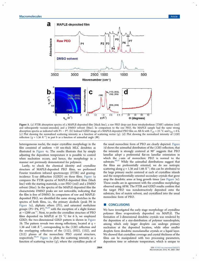
heterogeneous nuclei, the major crystalline morphology in thefilm consisted of uniform ∼10 nm-thick MLC dendrites asillustrated in Figure 4c. The results illustrate that by simplyadjusting the deposition temperature it is possible to controlwhen nucleation occurs, and hence, the morphology in amanner not previously demonstrated for polymers.Lastly, to check the chemical identity and crystalline
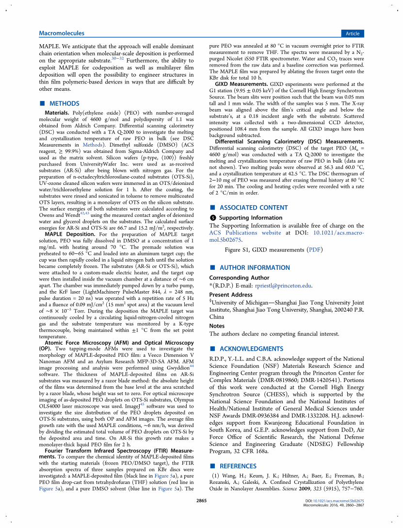
structure of MAPLE-deposited PEO films, we performedFourier transform infrared spectroscopy (FTIR) and grazing-incidence X-ray diffraction (GIXD) on these films. Figure 5acompares the FTIR spectra of MAPLE-deposited films (blackline) with the starting materials, a raw PEO (red) and a DMSOsolvent (blue). In the spectra of the MAPLE-deposited film thecharacteristic DMSO peaks are not noticeable, indicating thatthe film is free of DMSO. In comparison of raw and MAPLE-deposited PEO, we identified the same strong stretches in thespectra of both films, i.e., the primary alcohols (peak P6 inFigure 5a), aliphatic ethers (P5), and saturated methylenegroups (P1−P4, P7),38,39 with the exception of a slight featureat ∼1200 cm−1. Next, to probe the crystalline structure of PEOfilms deposited via MAPLE at 25 °C for 6 h, we employedGIXD; the two-dimensional GIXD pattern is shown in Figure5b. The pattern reveals two strong reflections, located at q =1.36 and 1.66 Å−1, corresponding to the (120) reflection andthe overlapping reflections of the (112), (032), (132), and(212) planes of the monoclinic PEO crystal structure,respectively.40,41 Figure 5c plots the scattering intensity as afunction of scattering vector (q), where the crystalline peaks of
the usual monoclinic form of PEO are clearly depicted. Figure5d shows the azimuthal distribution of the (120) reflection; thatthe intensity is strongly centered at 90° suggests that PEOlamellae adopt a preferential flat-on lamellar orientation inwhich the c-axis of monoclinic PEO is normal to thesubstrate.40,41 While the azimuthal distributions suggest thatthe films are preferentially oriented, we do see isotropicscattering along q = 1.36 and 1.66 Å−1; this can be attributed tothe large primary nuclei centered at each of crystalline islandsand the nonpreferentially oriented secondary crystals that growatop the dendritic arms at long growth times (see Figure 3e).These results are in agreement with the crystalline morphologyobserved using AFM. The FTIR and GIXD results confirm thatthe target PEO was nondestructively deposited onto thesubstrate, free of matrix solvent, and crystallized into the usualmonoclinic form of PEO.
■ CONCLUSIONS
We have investigated the early stage morphology of crystallinepolymer films evaporatively deposited via MAPLE. Theformation of 2-dimensional dendritic crystals was rendered bythe deposition of a size-distribution of polymer nanodroplets,among which only larger droplets can undergo primarynucleation at the deposited location, while other smallerdroplets form dendritic monolamellar crystals or a liquid layer.We showed that crystalline coverage and crystal thickness of thefilms can be manipulated with two processing parameters,deposition time or substrate temperature, which is unique to
Figure 5. (a) FTIR absorption spectra of a MAPLE-deposited film (black line), a raw PEO drop-cast from tetrahydrofuran (THF) solution (red)and subsequently vacuum-annealed, and a DMSO solvent (blue). In comparison to the raw PEO, the MAPLE sample had the same strongabsorption spectra as indicated with P1 − P7. (b) Indexed GIXD image of a MAPLE-deposited PEO film on AR-Si with Tsub = 25 °C and tdep = 6 h.(c) Plot showing the normalized scattering intensity as a function of scattering vector (q). (d) Plot showing the normalized intensity of (120)reflection (q = 1.36 Å−1) in part b as a function of azimuthal angle (Φ).
Macromolecules Article
DOI: 10.1021/acs.macromol.5b02675Macromolecules 2016, 49, 2860−2867
2864
MAPLE. We anticipate that the approach will enable dominantchain orientation when molecular-scale deposition is performedon the appropriate substrate.30−32 Furthermore, the ability toexploit MAPLE for codeposition as well as multilayer filmdeposition will open the possibility to engineer structures inthin film polymeric-based devices in ways that are difficult byother means.
■ METHODSMaterials. Poly(ethylene oxide) (PEO) with number-averaged
molecular weight of 4600 g/mol and polydispersity of 1.1 wasobtained from Aldrich Company. Differential scanning calorimetry(DSC) was conducted with a TA Q-2000 to investigate the meltingand crystallization temperature of raw PEO in bulk (see DSCMeasurements in Methods). Dimethyl sulfoxide (DMSO) (ACSreagent, ≥ 99.9%) was obtained from Sigma-Aldrich Company andused as the matrix solvent. Silicon wafers (p-type, ⟨100⟩) freshlypurchased from UniversityWafer Inc. were used as as-receivedsubstrates (AR-Si) after being blown with nitrogen gas. For thepreparation of n-octadecyltrichlorosilane-coated substrates (OTS-Si),UV-ozone cleaned silicon wafers were immersed in an OTS/deionizedwater/trichloroethylene solution for 1 h. After the coating, thesubstrates were rinsed and sonicated in toluene to remove multicoatedOTS layers, resulting in a monolayer of OTS on the silicon substrate.The surface energies of both substrates were calculated according toOwens and Wendt42,43 using the measured contact angles of deionizedwater and glycerol droplets on the substrates. The calculated surfaceenergies for AR-Si and OTS-Si are 66.7 and 15.2 mJ/m2, respectively.MAPLE Deposition. For the preparation of MAPLE target
solution, PEO was fully dissolved in DMSO at a concentration of 1mg/mL with heating around 70 °C. The premade solution waspreheated to 60−65 °C and loaded into an aluminum target cup; thecup was then rapidly cooled in a liquid nitrogen bath until the solutionbecame completely frozen. The substrates (AR-Si or OTS-Si), whichwere attached to a custom-made electric heater, and the target cupwere then installed inside the vacuum chamber at a distance of ∼6 cmapart. The chamber was immediately pumped down by a turbo pump,and the KrF laser (LightMachinery PulseMaster 844, λ = 248 nm,pulse duration = 20 ns) was operated with a repetition rate of 5 Hzand a fluence of 0.09 mJ/cm2 (15 mm2 spot area) at the vacuum levelof ∼8 × 10⁻⁵ Torr. During the deposition the MAPLE target wascontinuously cooled by a circulating liquid-nitrogen-cooled nitrogengas and the substrate temperature was monitored by a K-typethermocouple, being maintained within ±1 °C from the set pointtemperature.Atomic Force Microscopy (AFM) and Optical Microscopy
(OP). Two tapping-mode AFMs were used to investigate themorphology of MAPLE-deposited PEO film: a Veeco Dimension VNanoman AFM and an Asylum Research MFP-3D-SA AFM. AFMimage processing and analysis were performed using Gwyddion44
software. The thickness of MAPLE-deposited films on AR-Sisubstrates was measured by a razor blade method: the absolute heightof the films was determined from the base level at the area scratchedby a razor blade, whose height was set to zero. For optical microscopeimaging of as-deposited PEO droplets on OTS-Si substrates, OlympusOLS4000 laser microscope was used. ImageJ45 software was used toinvestigate the size distribution of the PEO droplets deposited onOTS-Si substrates, using both OP and AFM images. The average filmgrowth rate with the used MAPLE conditions, ∼6 nm/h, was derivedby dividing the estimated total volume of PEO droplets on OTS-Si bythe deposited area and time. On AR-Si this growth rate makes amonolayer-thick liquid PEO film for 2 h.Fourier Transform Infrared Spectroscopy (FTIR) Measure-
ments. To compare the chemical identity of MAPLE-deposited filmswith the starting materials (frozen PEO/DMSO target), the FTIRabsorption spectra of three samples prepared on KBr discs wereinvestigated: a MAPLE-deposited film (black line in Figure 5a), a purePEO film drop-cast from tetrahydrofuran (THF) solution (red line inFigure 5a), and a pure DMSO solvent (blue line in Figure 5a). The
pure PEO was annealed at 80 °C in vacuum overnight prior to FTIRmeasurement to remove THF. The spectra were measured by a N2-purged Nicolet iS50 FTIR spectrometer. Water and CO2 traces wereremoved from the raw data and a baseline correction was performed.The MAPLE film was prepared by ablating the frozen target onto theKBr disk for total 10 h.
GIXD Measurements. GIXD experiments were performed at theG1 station (9.95 ± 0.05 keV) of the Cornell High Energy SynchrotronSource. The beam slits were position such that the beam was 0.05 mmtall and 1 mm wide. The width of the samples was 5 mm. The X-raybeam was aligned above the film’s critical angle and below thesubstrate’s, at a 0.18 incident angle with the substrate. Scatteredintensity was collected with a two-dimensional CCD detector,positioned 108.4 mm from the sample. All GIXD images have beenbackground subtracted.
Differential Scanning Calorimetry (DSC) Measurements.Differential scanning calorimetry (DSC) of the target PEO (Mn =4600 g/mol) was conducted with a TA Q-2000 to investigate themelting and crystallization temperature of raw PEO in bulk (data arenot shown). Two melting peaks were observed at 56.3 and 60.0 °C,and a crystallization temperature at 42.5 °C. The DSC thermogram of2−10 mg of PEO was measured after erasing thermal history at 80 °Cfor 20 min. The cooling and heating cycles were recorded with a rateof 2 °C/min in order.
■ ASSOCIATED CONTENT
*S Supporting InformationThe Supporting Information is available free of charge on theACS Publications website at DOI: 10.1021/acs.macro-mol.5b02675.
Figure S1, GIXD measurements (PDF)
■ AUTHOR INFORMATION
Corresponding Author*(R.D.P.) E-mail: [email protected].
Present Address§University of MichiganShanghai Jiao Tong University JointInstitute, Shanghai Jiao Tong University, Shanghai, 200240 P.R.China
NotesThe authors declare no competing financial interest.
■ ACKNOWLEDGMENTS
R.D.P., Y.-L.L. and C.B.A. acknowledge support of the NationalScience Foundation (NSF) Materials Research Science andEngineering Center program through the Princeton Center forComplex Materials (DMR-0819860; DMR-1420541). Portionsof this work were conducted at the Cornell High EnergySynchrotron Source (CHESS), which is supported by theNational Science Foundation and the National Institutes ofHealth/National Institute of General Medical Sciences underNSF Awards DMR-0936384 and DMR-1332208. H.J. acknowl-edges support from Kwanjeong Educational Foundation inSouth Korea, and G.E.P. acknowledges support from DoD, AirForce Office of Scientific Research, the National DefenseScience and Engineering Graduate (NDSEG) FellowshipProgram, 32 CFR 168a.
■ REFERENCES(1) Wang, H.; Keum, J. K.; Hiltner, A.; Baer, E.; Freeman, B.;Rozanski, A.; Galeski, A. Confined Crystallization of PolyethyleneOxide in Nanolayer Assemblies. Science 2009, 323 (5915), 757−760.
Macromolecules Article
DOI: 10.1021/acs.macromol.5b02675Macromolecules 2016, 49, 2860−2867
2865
(2) Sharma, T.; Je, S.-S.; Gill, B.; Zhang, J. X. J. PatterningPiezoelectric Thin Film PVDF−TrFE Based Pressure Sensor forCatheter Application. Sens. Actuators, A 2012, 177, 87−92.(3) Fujitsuka, N.; Sakata, J.; Miyachi, Y.; Mizuno, K.; Ohtsuka, K.;Taga, Y.; Tabata, O. Monolithic Pyroelectric Infrared Image SensorUsing PVDF Thin Film. Sens. Actuators, A 1998, 66 (1−3), 237−243.(4) Ling, Q.-D.; Liaw, D.-J.; Zhu, C.; Chan, D. S.-H.; Kang, E.-T.;Neoh, K.-G. Polymer Electronic Memories: Materials, Devices andMechanisms. Prog. Polym. Sci. 2008, 33 (10), 917−978.(5) Heremans, P.; Gelinck, G. H.; Muller, R.; Baeg, K.-J.; Kim, D.-Y.;Noh, Y.-Y. Polymer and Organic Nonvolatile Memory Devices†.Chem. Mater. 2011, 23 (3), 341−358.(6) Liu, F.; Gu, Y.; Jung, J. W.; Jo, W. H.; Russell, T. P. On theMorphology of Polymer-Based Photovoltaics. J. Polym. Sci., Part B:Polym. Phys. 2012, 50 (15), 1018−1044.(7) Lee, S. S.; Loo, Y.-L. Structural Complexities in the Active Layersof Organic Electronics. Annu. Rev. Chem. Biomol. Eng. 2010, 1 (1), 59−78.(8) Bao, Z.; Dodabalapur, A.; Lovinger, A. J. Soluble and ProcessableRegioregular poly(3-hexylthiophene) for Thin Film Field-effectTransistor Applications with High Mobility. Appl. Phys. Lett. 1996,69 (26), 4108−4110.(9) Chang, J.-F.; Sun, B.; Breiby, D. W.; Nielsen, M. M.; Solling, T. I.;Giles, M.; McCulloch, I.; Sirringhaus, H. Enhanced Mobility of Poly(3-Hexylthiophene) Transistors by Spin-Coating from High-Boiling-Point Solvents. Chem. Mater. 2004, 16 (23), 4772−4776.(10) Yang, X.; Loos, J.; Veenstra, S. C.; Verhees, W. J. H.; Wienk, M.M.; Kroon, J. M.; Michels, M. A. J.; Janssen, R. A. J. NanoscaleMorphology of High-Performance Polymer Solar Cells. Nano Lett.2005, 5 (4), 579−583.(11) Yang, H.; Joo Shin, T.; Bao, Z.; Ryu, C. Y. Structural Transitionsof Nanocrystalline Domains in Regioregular poly(3-Hexyl Thiophene)Thin Films. J. Polym. Sci., Part B: Polym. Phys. 2007, 45 (11), 1303−1312.(12) Crossland, E. J. W.; Rahimi, K.; Reiter, G.; Steiner, U.; Ludwigs,S. Systematic Control of Nucleation Density in Poly(3-Hexylth-iophene) Thin Films. Adv. Funct. Mater. 2011, 21 (3), 518−524.(13) Pique, A.; McGill, R. A.; Chrisey, D. B.; Leonhardt, D.; Mslna,T. E.; Spargo, B. J.; Callahan, J. H.; Vachet, R. W.; Chung, R.; Bucaro,M. A. Growth of Organic Thin Films by the Matrix Assisted PulsedLaser Evaporation (MAPLE) Technique. Thin Solid Films 1999, 355−356, 536−541.(14) Chrisey, D. B.; Pique, A.; McGill, R. A.; Horwitz, J. S.;Ringeisen, B. R.; Bubb, D. M.; Wu, P. K. Laser Deposition of Polymerand Biomaterial Films. Chem. Rev. 2003, 103 (2), 553−576.(15) Shepard, K. B.; Priestley, R. D. MAPLE Deposition ofMacromolecules. Macromol. Chem. Phys. 2013, 214 (8), 862−872.(16) Li, A.; Dong, B. X.; Green, P. F. Influence of MorphologicalDisorder on in- and out-of-Plane Charge Transport in ConjugatedPolymer Films. MRS Commun. 2015, 5, 593.(17) Liu, Y.; Atewologun, A.; Stiff-Roberts, A. D. OrganicSemiconductor Thin Films Deposited by Resonant Infrared Matrix-Assisted Pulsed Laser Evaporation: A Fundamental Study of theEmulsion Target. MRS Online Proc. Libr. 2014, 1733, 957.(18) Califano, V.; Bloisi, F.; Vicari, L.; Barra, M.; Cassinese, A.;Fanelli, E.; Buzio, R.; Valbusa, U.; Carella, A.; Roviello, A. SubstrateTemperature Dependence of the Structure of Polythiophene ThinFilms Obtained by Matrix Assisted Pulsed Laser Evaporation(MAPLE). Eur. Phys. J.: Appl. Phys. 2009, 48 (01), 10505.(19) Hiszpanski, A. M.; Loo, Y.-L. Directing the Film Structure ofOrganic Semiconductors via Post-Deposition Processing for Transistorand Solar Cell Applications. Energy Environ. Sci. 2014, 7 (2), 592−608.(20) Guo, Y.; Morozov, A.; Schneider, D.; Chung, J. W.; Zhang, C.;Waldmann, M.; Yao, N.; Fytas, G.; Arnold, C. B.; Priestley, R. D.Ultrastable Nanostructured Polymer Glasses. Nat. Mater. 2012, 11 (4),337−343.(21) Shepard, K. B.; Arnold, C. B.; Priestley, R. D. Origins ofNanostructure in Amorphous Polymer Coatings via Matrix AssistedPulsed Laser Evaporation. Appl. Phys. Lett. 2013, 103 (12), 123105.
(22) Leveugle, E.; Zhigilei, L. V. Molecular Dynamics SimulationStudy of the Ejection and Transport of Polymer Molecules in Matrix-Assisted Pulsed Laser Evaporation. J. Appl. Phys. 2007, 102 (7),074914.(23) Leveugle, E.; Sellinger, A.; Fitz-Gerald, J. M.; Zhigilei, L. V.Making Molecular Balloons in Laser-Induced Explosive Boiling ofPolymer Solutions. Phys. Rev. Lett. 2007, 98 (21), 216101.(24) Leveugle, E.; Zhigilei, L. V.; Sellinger, A.; Fitz-Gerald, J. M.Computational and Experimental Study of the Cluster SizeDistribution in MAPLE. Appl. Surf. Sci. 2007, 253 (15), 6456−6460.(25) Liu, Y.-X.; Chen, E.-Q. Polymer Crystallization of UltrathinFilms on Solid Substrates. Coord. Chem. Rev. 2010, 254 (9−10),1011−1037.(26) Massa, M.; Dalnoki-Veress, K. Homogeneous Crystallization ofPoly(Ethylene Oxide) Confined to Droplets: The Dependence of theCrystal Nucleation Rate on Length Scale and Temperature. Phys. Rev.Lett. 2004, 92 (25), 255509.(27) Reiter, G.; Sommer, J.-U. Crystallization of Adsorbed PolymerMonolayers. Phys. Rev. Lett. 1998, 80 (17), 3771−3774.(28) Reiter, G. Some Unique Features of Polymer Crystallisation.Chem. Soc. Rev. 2014, 43 (7), 2055.(29) Zhu, D.-S.; Liu, Y.-X.; Chen, E.-Q.; Li, M.; Chen, C.; Sun, Y.-H.;Shi, A.-C.; Van Horn, R. M.; Cheng, S. Z. D. Crystal GrowthMechanism Changes in Pseudo-Dewetted Poly(ethylene Oxide) ThinLayers. Macromolecules 2007, 40 (5), 1570−1578.(30) Wang, Y.; Rafailovich, M.; Sokolov, J.; Gersappe, D.; Araki, T.;Zou, Y.; Kilcoyne, A.; Ade, H.; Marom, G.; Lustiger, A. SubstrateEffect on the Melting Temperature of Thin Polyethylene Films. Phys.Rev. Lett. 2006, 96 (2), 028303.(31) Ma, Y.; Hu; Reiter, G. Lamellar Crystal Orientations Biased byCrystallization Kinetics in Polymer Thin Films. Macromolecules 2006,39 (15), 5159−5164.(32) Lohmann, A.-K.; Henze, T.; Thurn-Albrecht, T. DirectObservation of Prefreezing at the Interface Melt−solid in PolymerCrystallization. Proc. Natl. Acad. Sci. U. S. A. 2014, 111 (49), 17368−17372.(33) Reiter, G.; Castelein, G.; Sommer, J.-U. Liquidlike Morpho-logical Transformations in Monolamellar Polymer Crystals. Phys. Rev.Lett. 2001, 86 (26), 5918−5921.(34) Braun, H.-G.; Meyer, E. Structure Formation of Ultrathin PEOFilms at Solid InterfacesComplex Pattern Formation by Dewettingand Crystallization. Int. J. Mol. Sci. 2013, 14 (2), 3254−3264.(35) Hwang, R.; Schroder, J.; Gunther, C.; Behm, R. Fractal Growthof Two-Dimensional Islands: Au on Ru(0001). Phys. Rev. Lett. 1991,67 (23), 3279−3282.(36) Barth, J. V.; Costantini, G.; Kern, K. Engineering Atomic andMolecular Nanostructures at Surfaces. Nature 2005, 437 (7059), 671−679.(37) Zhang, Z.; Lagally, M. G. Atomistic Processes in the Early Stagesof Thin-Film Growth. Science 1997, 276 (5311), 377−383.(38) Papke, B. L.; Ratner, M. A.; Shriver, D. F. VibrationalSpectroscopy and Structure of Polymer Electrolytes, Poly(ethyleneOxide) Complexes of Alkali Metal Salts. J. Phys. Chem. Solids 1981, 42(6), 493−500.(39) Lambert, J. B.; Shurvell, H. F.; Lightner, D. A.; Cooks, R. G.Organic Structural Spectroscopy; Prentice Hall: Upper Saddle River, NJ,1998.(40) Zhu, L.; Cheng, S. Z. D.; Calhoun, B. H.; Ge, Q.; Quirk, R. P.;Thomas, E. L.; Hsiao, B. S.; Yeh, F.; Lotz, B. CrystallizationTemperature-Dependent Crystal Orientations within NanoscaleConfined Lamellae of a Self-Assembled Crystalline−AmorphousDiblock Copolymer. J. Am. Chem. Soc. 2000, 122 (25), 5957−5967.(41) Asada, M.; Jiang, N.; Sendogdular, L.; Sokolov, J.; Endoh, M. K.;Koga, T.; Fukuto, M.; Yang, L.; Akgun, B.; Dimitriou, M.; Satija, S.Melt Crystallization/dewetting of Ultrathin PEO Films via CarbonDioxide Annealing: The Effects of Polymer Adsorbed Layers. SoftMatter 2014, 10 (34), 6392−6403.(42) Owens, D. K.; Wendt, R. C. Estimation of the Surface FreeEnergy of Polymers. J. Appl. Polym. Sci. 1969, 13 (8), 1741−1747.
Macromolecules Article
DOI: 10.1021/acs.macromol.5b02675Macromolecules 2016, 49, 2860−2867
2866

(43) Kim, C. S.; Tinker, L. L.; DiSalle, B. F.; Gomez, E. D.; Lee, S.;Bernhard, S.; Loo, Y.-L. Altering the Thermodynamics of PhaseSeparation in Inverted Bulk-Heterojunction Organic Solar Cells. Adv.Mater. 2009, 21 (30), 3110−3115.(44) Necas, D.; Klapetek, P. Gwyddion: An Open-Source Softwarefor SPM Data Analysis. Cent. Eur. J. Phys 2011, 10 (1), 181−188.(45) Schneider, C. A.; Rasband, W. S.; Eliceiri, K. W. NIH Image toImageJ: 25 Years of Image Analysis. Nat. Methods 2012, 9 (7), 671−675.
Macromolecules Article
DOI: 10.1021/acs.macromol.5b02675Macromolecules 2016, 49, 2860−2867
2867