additive manufacturing: making imagination the major ... · additive manufacturing: making...
TRANSCRIPT

Additive Manufacturing: Making Imagination theMajor Limitation
YUWEI ZHAI,1,3 DIANA A. LADOS,1,4 and JANE L. LAGOY2,5
1.—Integrative Materials Design Center (iMdc), Worcester Polytechnic Institute, 100 InstituteRoad, Worcester, MA 01609, USA. 2.—Bodycote IMT, Inc., 155 River Street, Andover, MA 01810,USA. 3.—e-mail: [email protected]. 4.—e-mail: [email protected]. 5.—e-mail: [email protected]
Additive manufacturing (AM) refers to an advanced technology used for thefabrication of three-dimensional near-net-shaped functional componentsdirectly from computer models, using unit materials. The fundamentals andworking principle of AM offer several advantages, including near-net-shapecapabilities, superior design and geometrical flexibility, innovative multi-material fabrication, reduced tooling and fixturing, shorter cycle time for de-sign and manufacturing, instant local production at a global scale, andmaterial, energy, and cost efficiency. Well suiting the requests of modernmanufacturing climate, AM is viewed as the new industrial revolution,making its way into a continuously increasing number of industries, such asaerospace, defense, automotive, medical, architecture, art, jewelry, and food.This overview was created to relate the historical evolution of the AM tech-nology to its state-of-the-art developments and emerging applications. Genericthoughts on the microstructural characteristics, properties, and performanceof AM-fabricated materials will also be discussed, primarily related to metallicmaterials. This write-up will introduce the general reader to specifics of theAM field vis-a-vis advantages and common techniques, materials and prop-erties, current applications, and future opportunities.
INTRODUCTION
Following the contour drawn by science fiction,the rapid development of modern technologies isturning fantasy into reality, challenging both sci-ence fiction writers and engineers to push theirimaginations further. Additive manufacturing (AM)technology, or three-dimensional (3D) printing, is akey enabler of this transformation.
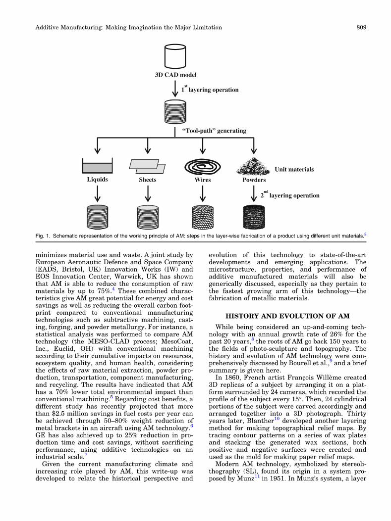
AM refers to a broad family of techniques thatturn 3D digital designs into actual functional partsin the same way an office printer places two-dimensional (2D) digital files onto pieces of paper.ASTM F2792 defines AM as ‘‘a process of joiningmaterials to make objects from 3D model data,usually layer upon layer, as opposed to subtractivemanufacturing methodologies.’’1 ASTM also speci-fies other commonly used synonyms for AM includ-ing additive fabrication, additive processes, additivetechniques, additive layer manufacturing, layermanufacturing, and freeform fabrication. The
general working principle of AM is schematicallyrepresented in Fig. 1.2 A 3D solid computer aideddesign (CAD) model is first sliced into layers togenerate digital information based on the geometryof each layer. This digital information then becomesthe tool path used to selectively combine unitmaterials, typically sheets, wires, and powderslayer by layer into final (near) net-shape objects.
This working principle offers AM technologysuperior flexibility. Complex shapes, such as inter-nal cooling channels that cannot be achieved bymachining, can be readily created by selectivelyplacing material only where is needed. The digitalmodels are not only freeform, but also can be sharedall over the world, which makes possible instantlocal production on a global scale.3 In addition, AMtechnology does not require molds, fixtures, ortooling, which effectively reduces the long lead timecaused by mold and/or tool design and manufac-turing. Near-net shaping is another important fea-ture of AM technology, which significantly
JOM, Vol. 66, No. 5, 2014
DOI: 10.1007/s11837-014-0886-2� 2014 The Minerals, Metals & Materials Society
808 (Published online March 11, 2014)
minimizes material use and waste. A joint study byEuropean Aeronautic Defence and Space Company(EADS, Bristol, UK) Innovation Works (IW) andEOS Innovation Center, Warwick, UK has shownthat AM is able to reduce the consumption of rawmaterials by up to 75%.4 These combined charac-teristics give AM great potential for energy and costsavings as well as reducing the overall carbon foot-print compared to conventional manufacturingtechnologies such as subtractive machining, cast-ing, forging, and powder metallurgy. For instance, astatistical analysis was performed to compare AMtechnology (the MESO-CLAD process; MesoCoat,Inc., Euclid, OH) with conventional machiningaccording to their cumulative impacts on resources,ecosystem quality, and human health, consideringthe effects of raw material extraction, powder pro-duction, transportation, component manufacturing,and recycling. The results have indicated that AMhas a 70% lower total environmental impact thanconventional machining.5 Regarding cost benefits, adifferent study has recently projected that morethan $2.5 million savings in fuel costs per year canbe achieved through 50–80% weight reduction ofmetal brackets in an aircraft using AM technology.6
GE has also achieved up to 25% reduction in pro-duction time and cost savings, without sacrificingperformance, using additive technologies on anindustrial scale.7
Given the current manufacturing climate andincreasing role played by AM, this write-up wasdeveloped to relate the historical perspective and
evolution of this technology to state-of-the-artdevelopments and emerging applications. Themicrostructure, properties, and performance ofadditive manufactured materials will also begenerically discussed, especially as they pertain tothe fastest growing arm of this technology—thefabrication of metallic materials.
HISTORY AND EVOLUTION OF AM
While being considered an up-and-coming tech-nology with an annual growth rate of 26% for thepast 20 years,8 the roots of AM go back 150 years tothe fields of photo-sculpture and topography. Thehistory and evolution of AM technology were com-prehensively discussed by Bourell et al.,9 and a briefsummary is given here.
In 1860, French artist Francois Willeme created3D replicas of a subject by arranging it on a plat-form surrounded by 24 cameras, which recorded theprofile of the subject every 15�. Then, 24 cylindricalportions of the subject were carved accordingly andarranged together into a 3D photograph. Thirtyyears later, Blanther10 developed another layeringmethod for making topographical relief maps. Bytracing contour patterns on a series of wax platesand stacking the generated wax sections, bothpositive and negative surfaces were created andused as the mold for making paper relief maps.
Modern AM technology, symbolized by stereoli-thography (SL), found its origin in a system pro-posed by Munz11 in 1951. In Munz’s system, a layer
3D CAD model
1st
layering operation
“Tool-path” generating
Unit materials
Liquids Sheets Wires Powders
2nd
layering operation
Fig. 1. Schematic representation of the working principle of AM: steps in the layer-wise fabrication of a product using different unit materials.2
Additive Manufacturing: Making Imagination the Major Limitation 809

of transparent photopolymer was selectively ex-posed and hardened according to the cross-section ofa scanned object using a piston mechanism. In 1968,Swainson12 proposed the use of laser beam tosolidify photosensitive polymers; parallel and simi-lar work was also conducted at Battelle Laborato-ries.13 Ciraud14 was the first to introduce in 1971the use of powders, which were partially melted,using laser, electron or plasma beams as heatsources. In 1981, Housholder15 described the earli-est ‘‘powder laser sintering’’ process without hav-ing it commercialized. At about the same time,Kodama16 from Nagoya Municipal IndustrialResearch Institute published the first rapid proto-typing system, using functional photopolymermaterials, while Herbert17 from 3M (St. Paul, MN)developed the earliest SL system that used a com-puter to command the ultraviolet laser beams.
AM technology has evolved significantly over thepast three decades, facilitating the launching ofmany AM companies. 3D Systems (Rock Hill, SC)was founded in 1986 by Charles Hull to commer-cialize the SL technique. The selective laser sinter-ing (SLS) method was developed at approximatelythe same time and led to the formation of DTM,which was acquired by 3D Systems in 2001.18
Stratasys (Eden Prairie, MN) was founded in the1990s, with the commercialization of the fuseddeposition modeling process. The freeform fabrica-tion of metallic objects then garnered major atten-tion, and many methodologies, including directmetal laser sintering (DMLS), laser-engineered netshaping (LENS), electron-beam melting (EBM), andothers were developed specifically for metals such asstainless steel, titanium, and nickel-base alloys. Aclassification of AM techniques is provided in theAppendix (Table I), together with a list of commonAM techniques, manufacturers, and equipmentvendors (Table II). A few techniques for fabricatingmetallic materials are highlighted in the followingsection.
DISCUSSION OF SELECTED METAL AMTECHNIQUES AND THEIR OPERATING
PRINCIPLES
Although it started from organic materials, AMtechnology found a special place in the manufac-turing of metallic materials by meeting therequirements for performance, enhanced manufac-turing efficiency, sustainability, and energy andcost savings. Numerous AM techniques have beendeveloped to capitalize on these important benefits,as detailed in the Appendix. Several of these tech-niques have been either developed specifically oradapted from polymer-based methods for the fabri-cation of metallic components. A classification ofmetal AM techniques based on heat source andmaterial feedstock is concisely presented here,together with basic operating principles of selectedprocesses in each class.
Powder Bed Fusion (Laser Beam/ElectronBeam/Inkjet Head+Powder Bed System)
Powder bed fusion technology started from SLSand has evolved into various techniques that havesimilar working principles but use different bindingmechanisms. Typical methods based on the combi-nation of laser beams and powder beds include theoriginal SLS owned by 3D Systems and the widelyused DMLS from EOS. A similar technique knownas LaserCUSING was trademarked by ConceptLaser (Lichtenfels, Germany), which also producestheir own series of machines.19 Substituting laserbeams with electron beams yields the EBM tech-nique developed by Arcam AB (Molndal, Sweden). Ifan inkjet head and a powder bed system are com-bined, the process is referred to as 3D printing,* aprocess developed at MIT and licensed to ZCorp(Rock Hill, SC) in 1995. As an example, the workingprinciple of DMLS is schematically represented inFig. 2.
The whole process assembly consists of a laserscanning system, a powder delivery piston, a roller,and a fabrication piston. Before fabrication starts,the powder delivery piston moves up and the fabri-cation piston moves down one layer thickness. Thepowder is spread and lightly compacted by the rollerover the surface of the fabrication piston, and a la-ser beam is then driven over it to selectively meltthe powder under the guidance of the scanner sys-tem. After each layer is completed, the fabricationpiston moves down another layer thickness and anew layer of powder is spread over. This processcontinues until the whole part is created. Uponfinishing, the fabrication piston rises up and ele-vates the final object; excess powder is brushedaway and partially reused after proper treat-ments.20 One of the advantages of the powder bedfusion systems is that support structures are notrequired. However, supports are often added toprovide thermal pathways for heat dissipation andbetter geometry control.
Direct Energy Deposition: Powder-BasedMethods (Laser Beam+Powder DeliveryNozzle)
In this class, powder bed systems are replaced bypowder delivery nozzles. There are two major tech-niques in this group: (I) LENS, developed at SandiaNational Laboratories in the 1990s and licensed toOptomec in 1997 (who has been the sole manufac-turer and distributor of LENS systems since then21)and (II) direct metal deposition (DMD) provided byPOM Group (Auburn Hills, MI). The main differ-ences between the two processes consist in thedetails of machine control and implementation;22
DMD also allows processing in open atmosphere
*The term 3D printing (3DP) here refers to the specific techniquethat was developed at MIT (Cambridge, MA). The term 3DP isalso commonly used as a synonym for additive manufacturing.
Zhai, Lados, and Lagoy810

using local shielding of the molten metal. The LENStechnique, for example, can process a wide range ofmetals, including titanium, nickel-base superalloys,and stainless and tool steels, which are all com-mercially available in powder form as required forthis process.23 A schematic representation of theLENS process is shown in Fig. 3.
A substrate is first placed onto the x–y motiontable. Then, a high-power focused laser beam cre-ates a melting pool on the substrate to which metalpowders are delivered coaxially. A metal powder–laser beam interaction zone is created to fuse themetal powders into a deposit. Typically, the x–ymotion table moves in a raster manner to fabricateeach layer of the object according to the CAD design,and the powder delivery nozzle moves upward uponcompleting each layer to start the deposition of anew layer. Metal powders are typically delivered
and distributed using an inert carrier gas to shieldthe molten metal pool from oxidation and to pro-mote layer-to-layer adhesion by providing bettersurface wetting.24
Direct Energy Deposition: Wire-Based Meth-ods (Electron Beam+Metal Wire Feedstock)
Direct energy deposition includes another class ofmetal AM techniques, which use solid wire feed-stock instead of powders. Electron beam freeformfabrication (EBF3) is one of the main techniquesbelonging to this class. EBF3 was developed byLockheed Martin (Bethesda, MD) in 1999 and dis-closed in 2002.25 This technology was extensivelystudied and improved at NASA Langley ResearchCenter (Hampton, VA) for producing unitizedstructures using aerospace materials such as
Sealed chamber
Powder delivery piston
Laser scanning system
Fabrication pistonRollers
Part
Fig. 2. Schematic representation of DMLS system.2
Laser beam
Material deposition headz motion
Deposition
Substrate
x-y table
Hermetically-sealed chamber
Fig. 3. Schematic representation of LENS process.2
Additive Manufacturing: Making Imagination the Major Limitation 811

aluminum, titanium, nickel-base alloys, titaniumaluminides, metal matrix composites, and high-strength steels.26 The EBF3 technique operates in asimilar fashion to LENS except that electron beamsare used as the heat source. EBF3 process is per-formed under a vacuum environment (10�4 torr orlower), and a metal wire feeding system is incorpo-rated to deliver feedstock to the molten pool off-axially. The electron beam can be controlled anddeflected very precisely and couples very effectivelywith highly reflective materials. This process has anefficiency of nearly 100% in wire consumption and95% in power usage.26 A schematic representationof the EBF3 system is shown in Fig. 4.
NASA Langley Research Center has two typesof EBF3 systems—ground based and portable. Theground-based system has a dual-wire feedingsystem, which can be loaded with either fine orcoarse wires for different feature definitions, orwith two different alloys to produce compositionalgradients or multimaterial components. The por-table system has a single-wire feeder, which canbe used for finer metal wire and has higher posi-tioning precision compared to the ground-basedsystem. These features make it ideal for the fab-rication of smaller parts with intricate details.26
NASA has two portable EBF3 machines, onethat has successfully flown on the microgravityresearch airplane and another that is beingdeveloped for potential in-space manufacturingactivities.
EXAMPLES OF AM APPLICATIONS ANDSUSTAINABILITY CONSIDERATIONS
The use of AM continues to expand as more ad-vanced AM techniques are being developed andimproved. One of the earliest applications of AMtechnology was the production of tools with specialcooling channels for plastic injection molding. To-day, AM technology is employed to make a variety ofproducts, including medical implants; orthopedicand dental parts; hearing aids; forming tools; aero-space, military, and automotive components; elec-tronics; video game avatars; art; jewelry;commercial lighting; three-dimensional textiles;food; and more. Current research is even delving
into biomedical applications with the utilization ofAM in living tissue generation.
As an example of the U.S. AM industry, thecompany Directed Manufacturing Inc. (DMI; Aus-tin, TX) depends heavily on the aerospace andmedical markets. DMI spun off from an R&D/pro-totyping venture in 2006 to commercialize the pro-duction use of AM. Currently at 10 AM machines,DMI plans to add one or two machines annually forthe foreseeable future as many customers haveconverted to AM from castings, forgings, multi-component assembling, or subtractive manufactur-ing (machining). Although some secondarymachining is often required for production parts, forcomplex part geometries, AM is considerably fasterand more economical compared with other manu-facturing methods.27
In the medical sector, AM is seen to have greatability to produce precise medical devices, such assurgical instruments28 and customized implants,including partial skull plates and joint replace-ments.29 It has also been successfully applied in theprosthetic industry to design and fabricate light-weight and low-cost robotic parts, such as handsand wrists, thus consolidating complex assembliesinto single parts.30 The military is also interested inAM’s portability and adaptive capabilities for mul-tiple in-field uses. Additional applications includeunmanned aerial vehicles, the next generation ofMars rovers, commercial airplane wing bracketsand cooling ducts, turbine engine blades, heatexchangers, and the repair of blades and dies.31–33
To realize its full potential, however, AM still needsto overcome the long and expensive process of get-ting qualifications, especially in the aerospace,military, and medical fields, which are the targetmarkets for high-dollar components and demandingstructural applications.26
For a specific automotive application, Daimler AG(Stuttgart, Germany) has partnered with ConceptLaser and Fraunhofer Institute of Laser Technologyto replace costly and time-consuming sand and diecasting processes used to make large metal func-tional components with AM fabrication methods forweight-optimized geometries.34 In an interestingtwist, the competing process of investment castingis looking to AM for streamlining their process ofdeveloping molds, including decreasing cost byreducing waste and eliminating tooling, increasingachievable complexity, and accelerating prototypedevelopment and production planning.35
In the jewelry field, precious metal designs bringsome unique challenges compared with more com-mon AM alloys because of the high-polished sur-faces desired by customers. Whereas cast jewelryactually requires less finishing, AM allows the cre-ation of designs never before achievable, givingartists and designers a new level of geometricaldetail never before seen.36 Similarly, art or anyindustry needing to recreate legacy components nolonger available now has the opportunity to image a
Vacuum chamber
Wire feeding system
EB system
Deposition
Substrate
Fig. 4. Schematic representation of EBF3 system.2
Zhai, Lados, and Lagoy812

piece, enter the data into an AM machine, and buildit anew.
In 2009, the Roadmap for Additive Manufacturing(RAM) Workshop was held in Washington, DC,where topics related to research needs and devel-oping trends were discussed by 65 invited experts.Energy and sustainability represented an impor-tant chapter in the workshop report, foreseeingAM’s positive impact on sustainability but lackingconcrete and complete sustainability assess-ments.37,38 In 2010, Sreenivasan et al.38 performedan overall energy assessment for SLS of polymers,using eco-indicators. The results have shown anenergy consumption distribution with approxi-mately 16% coming from the laser systems, 25%from feed and build piston, and 40% from powderfeed and partbed heaters. Better thermal manage-ment, elimination of powder heating, and adoptionof high-efficiency lasers were identified as potentialmethods for reducing energy consumption. Suchsystematic energy and sustainability assessmentsneed to be done for other AM techniques andapplications, including those relevant to metallicmaterials, to quantify their environmental advan-tages and open new opportunities and markets.
PROPERTIES AND PERFORMANCEOF ADDITIVE MANUFACTURED MATERIALS
Above and beyond cost, energy, and sustainabilityadvantages, the properties and performance of AMproducts are essential factors in evaluating the suit-ability of this technology, especially for critical appli-cations, including aerospace, ground transportation,and medical. In light of this fact, EWI organized thefirst U.S. Additive Manufacturing Consortium (AMC)in 2010 with 27 members including industry, govern-ment agencies, nonprofit research organizations, anduniversities to accelerate innovation. They identifiedfive key topics for improvement: (I) material propertydatabases, (II) process model compensation for dis-tortion/first time accuracy, (III) process sensing andcontrol and nondestructive evaluation, (IV) clear andaffordable paths to certification and qualification, and(V) bigger, faster, and more capable OEM equip-ment.39 Substantial financial investments have alsobeen made to support such endeavors, most recentlyby the inception of NAMII (National Additive Manu-facturing Innovation Institute), funded by the U.S.Department of Commerce (DOC), Department ofDefense (DOD),DepartmentofEnergy (DOE),NationalScience Foundation (NSF), and NASA, along withmultiple industrial, academic, and nonprofit partners.
Given that properties and performance are greatlyinfluenced by the materials’ internal characteristics, afundamental understanding of the microstructureevolution in different AM techniques is imperative.Extensive research has been conducted on variousadditive manufactured metallic materials,2,26,40 anddramatically different microstructures were observedcompared to conventionally manufactured materials.
These include distinct layer patterns and heat-af-fected zones, directional grains, and typically very finecharacteristic features inside the grains.
In LENS fabricated Ti-6Al-4V alloys,2 for example,large columnar grains parallel to the depositiondirection were observed as a result of heat extractionfrom the substrate, as shown in Fig. 5a–e. Macro-heat-affected zones (macro-HAZs) were found at theinterfaces between LENS depositions and substratesas illustrated in Fig. 5d and e. In addition and specificto AM, micro-heat-affected zones (lHAZs) withcoarser characteristic features were also observedbetween layers due to reheating of previous layersupon subsequent depositions.2 These lHAZs give AMmicrostructures their distinct ‘‘layered’’ appearanceas seen in Fig. 5a–c. Directional grains, macro-HAZ,and lHAZ yield nonuniform microstructures in AMmaterials, leading to property differences in variousorientations.2,41–44
The internal microstructural characteristics ofAM-fabricated metals, as well as their surface con-ditions, are affected by processing parameters.Thinner layers, finer columnar grains, smallerporosity, and narrower macro-HAZs and lHAZs wereobserved in LENS Ti-6Al-4V fabricated using lowpower (Fig. 5a, b, and d), versus high power (Fig. 5cand e).2 Low-power LENS fabrication also creates abetter surface finish (Fig. 6a and b), than high-powerfabrication (Fig. 6c and d), at the expense of slowermanufacturing speed.2 The type of heat source isanother factor that influences the microstructure andproperties of AM-fabricated materials.45
Compared with parts made by conventional manu-facturing processes, AM-fabricated components showpromising properties for most metallic materials.2,46–48
However, the presence of shrinkage porosity andresidual stress can affect their static and dynamicproperties depending on the applied AM technique andprocessing parameters. Thus, post-AM processing isanother important direction of investigation. Hot iso-static pressing and heat treatments are consideredeffective methods for eliminating porosity, relievingresidual stress, and recovering ductility. However, as aresult of specific processing conditions and hencecharacteristic microstructures, conventional postpro-cessing treatments may not always lead to the expectedproperties and behavior of the AM-fabricated materi-als.49 Moreover, when AM technology is applied forlaser cladding and repairing damaged or improperlymanufactured components, post-AM heat treatmentsare impractical because of the need to preserve base/substrate material properties. Therefore, achieving thedesired properties and performance of the materialsand components requires judicious selection of the AMprocess, as well as tailoring of the fabrication condi-tions, postprocessing conditions, and parameters.
FUTURE AND DEVELOPING TRENDS IN AM
Offering the advantages of fast and precise man-ufacturing as well as positive environmental
Additive Manufacturing: Making Imagination the Major Limitation 813

impacts compared to conventional fabrication tech-niques, AM technology is being referred to as thenew industrial revolution. However, to meet andexceed the property standards set by traditionalmanufacturing techniques, especially for criticalstructural applications, further improvements andsignificant qualification studies need to be
completed. Comprehensive investigations on thestatic, dynamic, and high-temperature properties ofAM materials must be systematically performed toestablish fundamental knowledge, build meaningfulprocessing-microstructure-property relationships,and develop integrated databases for use in com-putational modeling and design. Manufacturers
Fig. 5. Layered microstructures of as-deposited LENS Ti-6Al-4V fabricated using different laser powers: (a, b, d) 330 W and (c, e) 780 W—lowerpower fabrication features thinner layers, finer columnar grains, smaller porosity (circled), and narrower macro-HAZ and lHAZ. (a) represents a3D panoramic view of the low power AM deposition on a mill-annealed substrate.2
Fig. 6. Surface photographs of LENS Ti-6Al-4V fabricated using different laser powers: (a, b) 330 W and (c, d) 780 W—(a, c) panoramicmacroscopic views of LENS blocks showing qualitative surface roughness differences and (b, d) surface zoom-ins showing layer thicknessdifferences between low and high power conditions.2
Zhai, Lados, and Lagoy814

then need to take the next step in (I) optimizing theAM materials and techniques, and (II) developingmethods to inspect their products effectively. As anexample in this direction, GE signed a Joint Tech-nology Development Agreement (JTDA) with SigmaLabs (Santa Fe, NM) to implement in-processinspection technologies, which are anticipated toimprove quality and increase additive productionrates by 25%.50
From Star Trek’s ‘‘Replicator’’ to large manufac-turing facilities and military in-the-field portablefabrication51 to personal offices52 and the foodindustry,53 AM is finding its way in a wide range ofapplications, playing the role of ‘‘mass customiza-tion.’’ AM technology not only is used to manufac-ture critical components such as turbine blades,medical devices, and other complex structural partsbut also is used by enterprising fabricators to pro-duce 3D printed functional clocks, guns, robots, andeven 3D printer parts (the RepRap project). Animportant developing trend of AM is to grow per-sonal uses, which makes this technology even moreattractive, as Wohlers5 so revealingly stated: ‘‘Now,using AM, almost anyone located almost any-where—even in a college dormitory or spare room ina home—can become a manufacturer.’’
ACKNOWLEDGEMENTS
The authors thank the consortium members ofthe Integrative Materials Design Center (iMdc) forsupporting the AM research at WPI and BenetLaboratories for providing LENS Ti-6Al-4V mate-rials and valuable technical discussions.
REFERENCES
1. ASTM F2792-12a, Standard Terminology for AdditiveManufacturing Technologies, vol. 10.04.
2. Y. Zhai and D.A. Lados, Integrative Materials Design Center(iMdc), Bi-annual Progress Report (Worcester, MA: WPI,2012).
3. T.A. Campbell, C.B. Williams, O.S. Ivanova, and B. Garrett,Could 3D Printing Change the World? Atlantic Council.http://www.atlanticcouncil.org/publications/reports/could-3d-printing-change-the-world. Accessed 10 Jan 2014.
4. Additive Manufacturing Study Shows Cuts in Material Con-sumption and Reduced CO2 Emissions, Powder Metall. Rev.http://www.ipmd.net/articles/002490.html. Accessed 7 Jan 2014.
5. N. Serres, D. Tidu, and S. Sankare, J. Clean. Prod. 19, 1117(2011).
6. T. Wohlers, Manuf. Eng. 146, 70 (2011).7. GE Asks Maker Community to Push the Boundaries of What
is 3D Printable, Launching Open Engineering Quests(MarketWatch 2013). http://www.marketwatch.com/story/ge-asks-maker-community-to-push-the-boundaries-of-what-is-3d-printable-launching-open-engineering-quests-2013-06-11. Accessed 24 Feb 2014.
8. T. Wohlers, Wohlers Report 2011 (Fort Collins, CO: WohlersAssociates, 2011).
9. D.L. Bourell, J.J. Beaman, Jr., M.C. Leu, and D.W. Rosen, ABrief History of Additive Manufacturing and the 2009 Road-map for Additive Manufacturing: Looking Back and LookingAhead (US, Turkey Workshop on Rapid Technologies, 2009).
10. J.E. Blanther, U.S. patent 473,901 (1892).11. O.J. Munz, U.S. patent 2,775,758 (1956).12. W.K. Swainson, U.S. patent 4,041,476 (1977).13. R.E. Schwerzel, V.E. Wood, V.D. McGinniss, and C.M.
Verber, Proc. SPIE 90 (1984).14. A. Ciraud, Process and Device for the Manufacture of any
Objects Desired from any Meltable Material, FRG Disclo-sure Publication 2263777, 1972.
15. R.F. Housholder, U.S. patent 4,247,508 (1981).16. H. Kodama, Rev. Sci. Instrum. 52, 1770 (1981).17. A.J. Herbert, J. Appl. Photogr. Eng. 8, 185 (1982).18. A. Lou and C. Grosvenor, Selective Laser Sintering, Birth of
an Industry (Austin, University of Texas, 2012). http://www.me.utexas.edu/news/2012/0712_sls_history.php#ch4. Accessed22 Mar 2013.
19. Machine Solutions. http://www.concept-laser.de/en/industry/aerospace/machines.html. Accessed 13 May 2013.
20. Laser Sintering. http://www.additive3d.com/sls.htm. Accessed10 May 2013.
21. R.R. Mudge and N.R. Wald, Weld. J. 86, 44 (2007).22. Direct Additive Fabrication of Metal Parts and Injection
Molds. http://www.additive3d.com/tl_221a.htm#dmds. Accessed9 May 2013.
23. LENS Technology. http://www.optomec.com/Additive-Manufacturing-Technology/Laser-Additive-Manufacturing.Accessed 13 May 2013.
24. Laser Powder Forming. http://www.additive3d.com/lens.htm. Accessed 9 May 2013.
25. C.A. Brice and D.S. Henn (Paper presented at the Inter-national Institute of Welding Conference, Copenhagen,Denmark, 2002).
26. K.M. Taminger and R.A. Hafley, Electron Beam FreeformFabrication for Cost Effective Near-Net Shape Manufac-turing. CASI, 2006.
27. A. Fima, Directed Manufacturing, Inc., Austin, TX, privatecommunication, April 2013.
28. Additive Manufacturing Market (2012–2017), Markets andMarkets. http://www.marketsandmarkets.com/Market-Reports/additive-manufacturing-medical-devices-market-843.html.Accessed 10 Sept 2013.
29. POM Group, Inc., Precision Additive Manufacturing ofMedical Devices, White Paper (Auburn Hills, MI: The POMGroup, Inc.). http://www.nist.gov/tip/wp/pswp/upload/129_precision_additive_manufacturing_of_medical_device.pdf.Accessed 10 Sept 2013.
30. Assem. Automat. Mini Feat. 31(3) (2011).31. A.R. Thryft, Unmanned Aerial Vehicles Fly Via Additive
Manufacturing. www.designnews.com/author.asp?section_id=1386&doc_id=235660. Accessed 4 Jan 2012.
32. A.R. Thryft, 3D Printing Flies High. www.designnews.com/author.asp?section_id=1392&doc_id=251526. Accessed 17July 2013.
33. J.L. LaGoy, MS&T 2011 Conference Internal Bodycote TripReport (Westerville, OH: MS&T, 2011).
34. A.R. Thryft, Daimler Funds 3D Printer for Auto Production.www.designnews.com/author.asp?section_id=1392&doc_id=256731. Accessed 17 July 2013.
35. R. Brooks, Molding Concept May Speed Investment Casting.www.foundrymag.com/Classes/Article/ArticleDraw.aspx?CID=88814&Refresh=1. Accessed 17 July 2013.
36. J. Strauss, HJE Company, Inc., Queensbury, NY, USA,private communication, April 2013.
37. D.L. Bourell, M.C. Leu, and D.W. Rosen (Paper presented at theRoadmap for Additive Manufacturing (RAM) Workshop, 2009).
38. R. Sreenivasan, A. Goel, and D.L. Bourell, Phys. Procedia 5,81 (2010).
39. Additive Manufacturing Consortium. http://ewi.org/additive-manufacturing-consortium. Accessed 24 Sept 2013.
40. L.E. Murr, S.M. Gaytan, D.A. Ramirez, E. Martinez, J.Hernandez, K.N. Amato, P.W. Shindo, F.R. Medina, andR.B. Wicker, J. Mater. Sci. Technol. 28, 1 (2012).
41. R.S. Amano and P.K. Rohatgi, Mater. Sci. Eng. A 528, 6680(2011).
Additive Manufacturing: Making Imagination the Major Limitation 815

42. K. Kempen, E. Yasa, L. Thijs, J.-P. Kruth, and J. VanHumbeeck, Phys. Procedia 12A, 255 (2011).
43. L. Thijs, F. Verhaeghe, and T. Craeghs, Acta Mater. 58, 3303(2010).
44. X. Wu, J. Liang, and J. Mei, Mater. Des. 25, 137 (2004).45. B. Baufeld, E. Brandl, and O. van der Biest, J. Mater. Pro-
cess. Technol. 211, 1146 (2011).46. P. Ganesh, R. Kaul, and C.P. Paul, Mater. Sci. Eng. A 527,
7490 (2010).47. E. Chlebus, B. Kuznicka, and T. Kurzynowski, Mater.
Character. 62, 488 (2011).48. P.L. Blackwell and A. Wisbey, J. Mater. Process. Technol.
170, 268 (2005).49. B. Vrancken, L. Thijs, and J. Kruth, J. Alloys Compd. 541,
177 (2012).
50. GE Aviation Signs Additive Manufacturing CooperativeAgreement with Sigma Labs. http://www.geaviation.com/press/other/other_20130524.html. Accessed 13 Jan2014.
51. D.J. Hill, 3D Printing on the Frontlines—Army Developing$2.8 M Mobile Fabrication Labs. http://singularityhub.com/2013/02/28/3d-printing-on-the-frontlines-army-deploying-2-8m-mobile-fabrication-labs/. Accessed 13 Jan 2014.
52. S. Essaid, Make Your Own Products: 3D Printing ReachesConsumers. http://techland.time.com/2013/01/15/make-yourself-into-an-action-figure-3d-printing-reaches-consumers/. Accessed20 Feb 2014.
53. K. Baker, Order 3D Printed Pasta at Google’s Cafeterias.http://www.psfk.com/2012/08/3d-printed-pasta-google-cafeteria.html. Accessed 24 Feb 2014.
Table I. Classification of AM techniques based on input material
LOM: Laminated Object ManufacturingEBF3: Electron Beam Free Form FabricationFDM: Fused Deposition ModelingSL: Stereolithography3DP: 3D Printing
LPB: Laser Powder Bed – including Selective Laser Sintering (SLS), Direct Metal Laser Sintering (DMLS), and LaserCUSINGEBM: Electron Beam MeltingLENS: Laser Engineered Net Shaping
Table II. Operating principles and representative manufacturers/equipment vendors
AM process Acronym Representative vendors Operating principle
Direct metal laser sintering/selective laser melting
DMLS/SLM EOS renishaw Powder bed + laser beam
LaserCUSING LaserCUSING Concept laserElectron beam melting EBM Arcam AB Powder bed + electron beamLaser engineered net shaping LENS Optomec Metal powder (nozzle
delivered) + laser beamDirect metal deposition DMD DM3D technology(formerly POM group)
Laser powder deposition LPD Huffman Corp.Fused deposition modeling FDM Stratasys Filament material + laser
beamElectron beam freeform
fabricationEBF3 Sciaky, Inc. Metal wire + electron beam
3D printing 3DP 3D systems ExOne Powder bed + inkjet headStereolithography SL 3D systems Liquid photopolymer + UV/
laser beam
APPENDIX: Additive Manufacturing Techniques, Operating Principles, and RepresentativeManufacturers/Equipment Vendors
Zhai, Lados, and Lagoy816