adjustable precision shunt regulators - nexperia family adjustable precision shunt regulators rev. 6...
TRANSCRIPT
TL431 familyAdjustable precision shunt regulatorsRev. 6 — 9 January 2019 Product data sheet
1. Product profile
1.1. General descriptionThree-terminal shunt regulator family with an output voltage range between Vref = 2.495 V and 36 V, to be set by two external resistors.
Table 1. Product overviewTemperature range (Tamb)Reference voltage
tolerance (Vref) 0 °C to 70 °C -40 °C to 85 °C -40 °C to 125 °CPinning configuration(see Table 5)
TL431QDBZR normal pinning
TL431FDT normal pinning
2.0 % TL431CDBZR TL431IDBZR
TL431MFDT mirrored pinning
TL431AQDBZR normal pinning
TL431AFDT normal pinning
1.0 % TL431ACDBZR TL431AIDBZR
TL431AMFDT mirrored pinning
TL431BQDBZR normal pinning
TL431BFDT normal pinning
0.5 % TL431BCDBZR TL431BIDBZR
TL431BMFDT mirrored pinning
1.2. Features and benefits• Programmable output voltage up to 36 V• Three different reference voltage tolerances:• • Standard grade: 2 %
• A-Grade: 1 %• B-Grade: 0.5 %
• Typical temperature drift: 9 mV (in a range of 0 °C up to 70 °C)• Low output noise• Typical output impedance: 0.2 Ω• Sink current capability: 1 mA to 100 mA• AEC-Q100 qualified (grade 1)
Nexperia TL431 familyAdjustable precision shunt regulators
1.3. Applications• Shunt regulator• Precision current limiter• Precision constant current sink• Isolated feedback loop for Switch Mode Power Supply (SMPS)
1.4. Quick reference data
Table 2. Quick reference dataSymbol Parameter Conditions Min Typ Max UnitVKA cathode-anode voltage Vref - 36 V
IK cathode current 1 - 100 mA
reference voltage
• Standard-Grade (2.0 %) 2440 2495 2550 mV
• A-Grade (1.0 %) 2470 2495 2520 mV
Vref
• B-Grade (0.5 %)
VKA = Vref; IK = 10 mA;Tamb = 25 °C
2483 2495 2507 mV
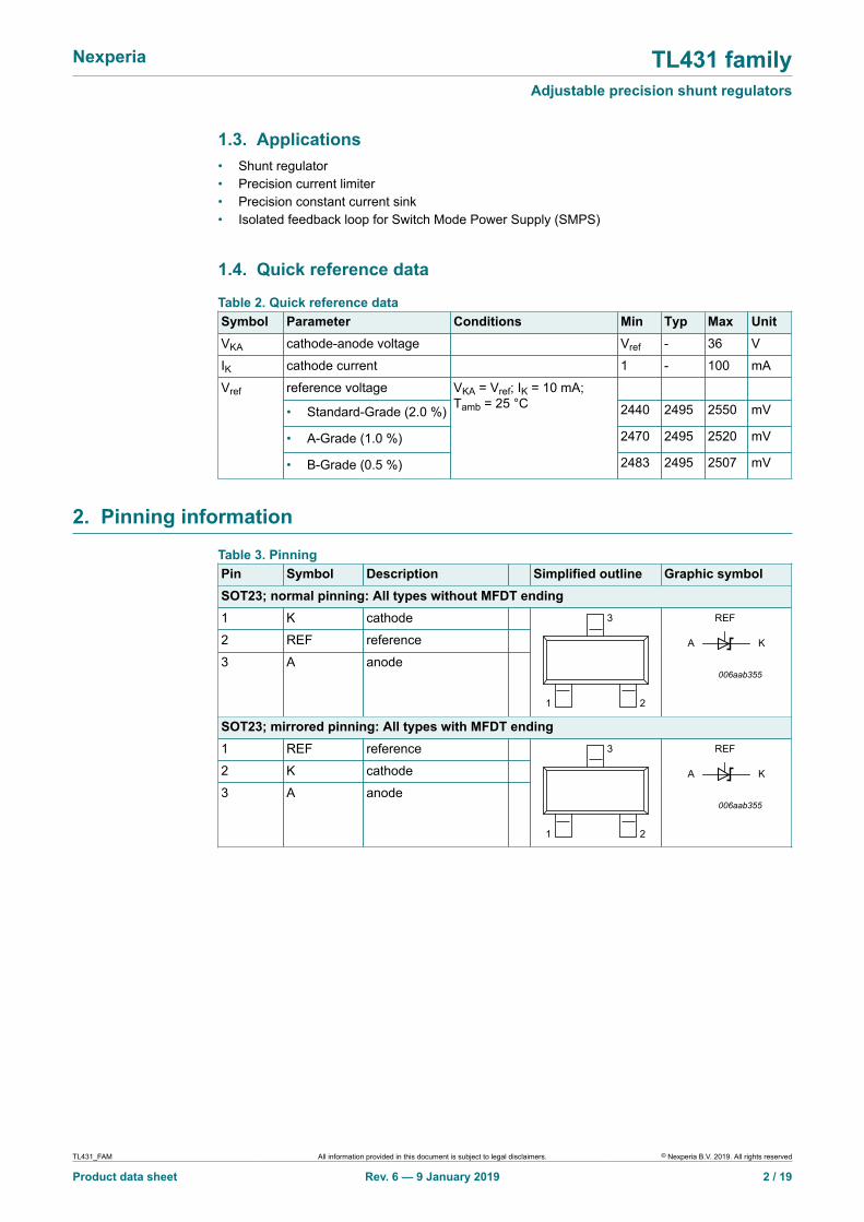
2. Pinning information
Table 3. PinningPin Symbol Description Simplified outline Graphic symbolSOT23; normal pinning: All types without MFDT ending1 K cathode
2 REF reference
3 A anode
1 2
3
006aab355
REF
A K
SOT23; mirrored pinning: All types with MFDT ending1 REF reference
2 K cathode
3 A anode
1 2
3
006aab355
REF
A K
TL431_FAM All information provided in this document is subject to legal disclaimers. © Nexperia B.V. 2019. All rights reserved
Product data sheet Rev. 6 — 9 January 2019 2 / 19
Nexperia TL431 familyAdjustable precision shunt regulators
3. Ordering information
Table 4. Ordering informationPackageType numberName Description Version
TL431CDBZR
TL431IDBZR
TL431QDBZR
TL431FDT
TL431MFDT
TL431ACDBZR
TL431AIDBZR
TL431AQDBZR
TL431AFDT
TL431AMFDT
TL431BCDBZR
TL431BIDBZR
TL431BQDBZR
TL431BFDT
TL431BMFDT
TO-236AB plastic surface-mounted package; 3 leads SOT23
4. Marking
Table 5. Marking codesType number Marking code [1] Type number Marking code [1]TL431CDBZR CA% TL431AFDT AS%
TL431IDBZR CB% TL431AMFDT AV%
TL431QDBZR CC% TL431BCDBZR CG%
TL431FDT AR% TL431BIDBZR CH%
TL431MFDT AU% TL431BQDBZR CJ%
TL431ACDBZR CD% TL431BFDT AT%
TL431AIDBZR CE% TL431BMFDT AW%
TL431AQDBZR CF% - -
[1] % = placeholder for manufacturing site code.
TL431_FAM All information provided in this document is subject to legal disclaimers. © Nexperia B.V. 2019. All rights reserved
Product data sheet Rev. 6 — 9 January 2019 3 / 19
Nexperia TL431 familyAdjustable precision shunt regulators
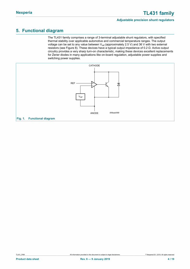
5. Functional diagramThe TL431 family comprises a range of 3-terminal adjustable shunt regulators, with specifiedthermal stability over applicable automotive and commercial temperature ranges. The outputvoltage can be set to any value between Vref (approximately 2.5 V) and 36 V with two externalresistors (see Figure 8). These devices have a typical output impedance of 0.2 Ω. Active outputcircuitry provides a very sharp turn-on characteristic, making these devices excellent replacementsfor Zener diodes in many applications like on-board regulation, adjustable power supplies andswitching power supplies.
Vref
ANODE
CATHODE
REF
006aab569
Fig. 1. Functional diagram
TL431_FAM All information provided in this document is subject to legal disclaimers. © Nexperia B.V. 2019. All rights reserved
Product data sheet Rev. 6 — 9 January 2019 4 / 19
Nexperia TL431 familyAdjustable precision shunt regulators
6. Limiting values
Table 6. Limiting valuesIn accordance with the Absolute Maximum Rating System (IEC 60134).
Symbol Parameter Conditions Min Max UnitVKA cathode-anode voltage - 37 V
IK cathode current -100 150 mA
Iref reference current -0.05 10 mA
total power dissipation [1] - 350 mW
[2] - 580 mW
Ptot Tamb ≤ 25 °C
[3] - 950 mW
Tj junction temperature - 150 °C
ambient temperature
TL431XCDBZR 0 +70 °C
TL431XIDBZR -40 +85 °C
Tamb
TL431XQDBZRTL431XFDT
-40 +125 °C
Tstg storage temperature -65 +150 °C
[1] Device mounted on an FR4 Printed-Circuit Board (PCB), single-sided copper, tin-plated and standardfootprint.
[2] Device mounted on an FR4 PCB, single-sided copper, tin-plated, mounting pad for anode 1 cm2.[3] Device mounted on a ceramic PCB, Al2O3, standard footprint.
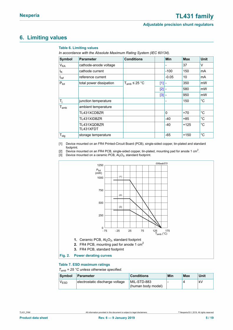
Tamb (°C)- 75 17512525 75- 25
006aab570
500
750
250
1000
1250
Ptot (mW)
0
(1)
(2)
(3)
1. Ceramic PCB, Al2O3, standard footprint2. FR4 PCB, mounting pad for anode 1 cm2
3. FR4 PCB, standard footprint
Fig. 2. Power derating curves
Table 7. ESD maximum ratingsTamb = 25 °C unless otherwise specified.
Symbol Parameter Conditions Min Max UnitVESD electrostatic discharge voltage MIL-STD-883
(human body model)- 4 kV
TL431_FAM All information provided in this document is subject to legal disclaimers. © Nexperia B.V. 2019. All rights reserved
Product data sheet Rev. 6 — 9 January 2019 5 / 19
Nexperia TL431 familyAdjustable precision shunt regulators
7. Recommended operating conditions
Table 8. Operating conditionsSymbol Parameter Conditions Min Max UnitVKA cathode-anode voltage Vref 36 V
IK cathode current 1 100 mA
8. Thermal characteristics
Table 9. Thermal characteristicsSymbol Parameter Conditions Min Typ Max Unit
[1] - - 360 K/W
[2] - - 216 K/W
Rth(j-a) thermal resistance fromjunction to ambient
[3] - - 132 K/W
Rth(j-sp) thermal resistance fromjunction to solder point
in free air
[4] - - 50 K/W
[1] Device mounted on an FR4 PCB, single-sided copper, tin-plated and standard footprint.[2] Device mounted on an FR4 PCB, single-sided copper, tin-plated, mounting pad for anode 1 cm2.[3] Device mounted on a ceramic PCB, Al2O3, standard footprint.[4] Soldering point of anode.
TL431_FAM All information provided in this document is subject to legal disclaimers. © Nexperia B.V. 2019. All rights reserved
Product data sheet Rev. 6 — 9 January 2019 6 / 19

Nexperia TL431 familyAdjustable precision shunt regulators
9. Characteristics
Table 10. CharacteristicsTamb = 25 °C unless otherwise specified.
Symbol Parameter Conditions Min Typ Max UnitStandard-Grade (2.0 %): TL431CDBZR; TL431IDBZR; TL431QDBZR; TL431FDT; TL431MFDT
Vref reference voltage VKA = Vref; IK = 10 mA 2440 2495 2550 mV
reference voltage variation VKA = Vref; IK = 10 mA
TL431CDBZR Tamb = 0 °C to 70 °C - 9 16 mV
TL431IDBZR Tamb = -40 °C to 85 °C
TL431QDBZR
TL431FDT
ΔVref
TL431MFDT
Tamb = -40 °C to 125 °C
- 17 34 mV
IK = 10 mA
ΔVKA = 10 V to Vref - -1.4 -2.7 mV/V
ΔVref/ΔVKA reference voltage variationto cathode -anode voltagevariation ratio
ΔVKA = 36 V to 10 V - -1 -2 mV/V
Iref reference current IK = 10 mA;R1 = 10 kΩ; R2 = open
- 2 4 μA
reference current variation IK = 10 mA; R1 = 10 kΩ; R2 = open
TL431CDBZR Tamb = 0 °C to 70 °C - 0.4 1.2 μA
TL431IDBZR Tamb = -40 °C to 85 °C
TL431QDBZR
TL431FDT
ΔIref
TL431MFDT
Tamb = -40 °C to 125 °C
- 0.8 2.5 μA
IK(min) minimum cathode current VKA = Vref - 0.4 1 mA
Ioff off-state current VKA = 36 V; Vref = 0 - 0.1 1 μA
ZKA dynamic cathode-anodeimpedance
IK = 0.1 mA to 100 mA;VKA = Vref; f < 1 kHz
- 0.20 0.5 Ω
A-Grade (1 %): TL431ACDBZR; TL431AIDBZR; TL431AQDBZR; TL431AFDT; TL431AMFDT
Vref reference voltage VKA = Vref; IK = 10 mA 2470 2495 2520 mV
reference voltage variation VKA = Vref; IK = 10 mA
TL431ACDBZR Tamb = 0 °C to 70 °C - 9 16 mV
TL431AIDBZR Tamb = -40 °C to 85 °C
TL431AQDBZR
TL431AFDT
ΔVref
TL431AMFDT
Tamb = -40 °C to 125 °C
- 17 34 mV
IK = 10 mA
ΔVKA = 10 V to Vref - -1.4 -2.7 mV/V
ΔVref/ΔVKA reference voltage variationto cathode-anode voltagevariation ratio
ΔVKA = 36 V to 10 V - -1.0 -2.0 mV
Iref reference current IK = 10 mA;R1 = 10 kΩ; R2 = open
- 2.0 4.0 μA
TL431_FAM All information provided in this document is subject to legal disclaimers. © Nexperia B.V. 2019. All rights reserved
Product data sheet Rev. 6 — 9 January 2019 7 / 19
Nexperia TL431 familyAdjustable precision shunt regulators
Symbol Parameter Conditions Min Typ Max Unitreference current variation IK = 10 mA; R1 = 10 kΩ; R2 = open
TL431ACDBZR Tamb = 0 °C to 70 °C - 0.4 1.2 μA
TL431AIDBZR Tamb = -40 °C to 85 °C
TL431AQDBZR
TL431AFDT
ΔIref
TL431AMFDT
Tamb = -40 °C to 125 °C
- 0.8 2.5 μA
minimum cathode current VKA = Vref
TL431ACDBZR Tamb = 0 °C to 70 °C
TL431AIDBZR Tamb = -40 °C to 85 °C
TL431AQDBZR
TL431AFDT
IK(min)
TL431AMFDT
Tamb = -40 °C to 125 °C
- 0.4 0.6 mA
Ioff off-state current VKA = 36 V; Vref = 0 - 0.1 0.5 μA
ZKA dynamic cathode-anodeimpedance
IK = 0.1 mA to 100 mA;VKA = Vref; f < 1 kHz
- 0.2 0.5 Ω
B-Grade (0.5 %): TL431BCDBZR; TL431BIDBZR; TL431BFDT; TL431BMFDT
Vref reference voltage VKA = Vref; IK = 10 mA 2483 2495 2507 mV
reference voltage variation VKA = Vref; IK = 10 mA
TL431BCDBZR Tamb = 0 °C to 70 °C - 9 16 mV
TL431BIDBZR Tamb = -40 °C to 85 °C
TL431BQDBZR
TL431BFDT
ΔVref
TL431BMFDT
Tamb = -40 °C to 125 °C
- 17 34 mV
IK = 10 mA
ΔVKA = 10 V to Vref - -1.4 -2.7 mV/V
ΔVref/ΔVKA reference voltage variationto cathode-anode voltagevariation ratio
ΔVKA = 36 V to 10 V - -1.0 -2.0 mV/V
Iref reference current IK = 10 mA;R1 = 10 kΩ; R2 = open
- 2.0 4.0 μA
reference current variation IK = 10 mA; R1 = 10 kΩ; R2 = open
TL431BCDBZR Tamb = 0 °C to 70 °C - 0.4 1.2 μA
TL431BIDBZR Tamb = -40 °C to 85 °C
TL431BQDBZR
TL431BFDT
ΔIref
TL431BMFDT
Tamb = -40 °C to 125 °C
- 0.8 2.5 μA
minimum cathode current VKA = Vref
TL431BCDBZR Tamb = 0 °C to 70 °C
TL431BIDBZR Tamb = -40 °C to 85 °C
TL431BQDBZR
TL431BFDT
IK(min)
TL431BMFDT
Tamb = -40 °C to 125 °C
- 0.4 0.6 mA
Ioff off-state current VKA = 36 V; Vref = 0 - 0.1 0.5 μA
ZKA dynamic cathode-anodeimpedance
IK = 0.1 mA to 100 mA;VKA = Vref; f < 1 kHz
- 0.2 0.5 Ω
TL431_FAM All information provided in this document is subject to legal disclaimers. © Nexperia B.V. 2019. All rights reserved
Product data sheet Rev. 6 — 9 January 2019 8 / 19
Nexperia TL431 familyAdjustable precision shunt regulators
Tamb (°C)-75 12575-25 25
aaa-028484
2.48
2.52
2.44
2.56
2.60
Vref(V)
2.40
IK = 10 mA; VKA = Vref
Fig. 3. Reference voltage as a function of ambienttemperature; typical values
VKA (V)- 2 320 1- 1
006aab572
0
50
- 50
100
150
IK (mA)
- 100
VKA = Vref; Tamb = 25 °C
Fig. 4. Cathode current as a function of cathode-anodevoltage; typical values
006aab573
GND
Vref
VKAINPUT
IK
IK = 10 mA; VKA = Vref
Fig. 5. Test circuit to Figures 3 and 4Tamb (°C)
-75 12575-25 25
aaa-028485
2
3
1
4
5
Iref(µA)
0
IK = 10 mA; R1 = 10 kΩ; R2 = open
Fig. 6. Reference current as a function of ambienttemperature; typical values
TL431_FAM All information provided in this document is subject to legal disclaimers. © Nexperia B.V. 2019. All rights reserved
Product data sheet Rev. 6 — 9 January 2019 9 / 19
Nexperia TL431 familyAdjustable precision shunt regulators
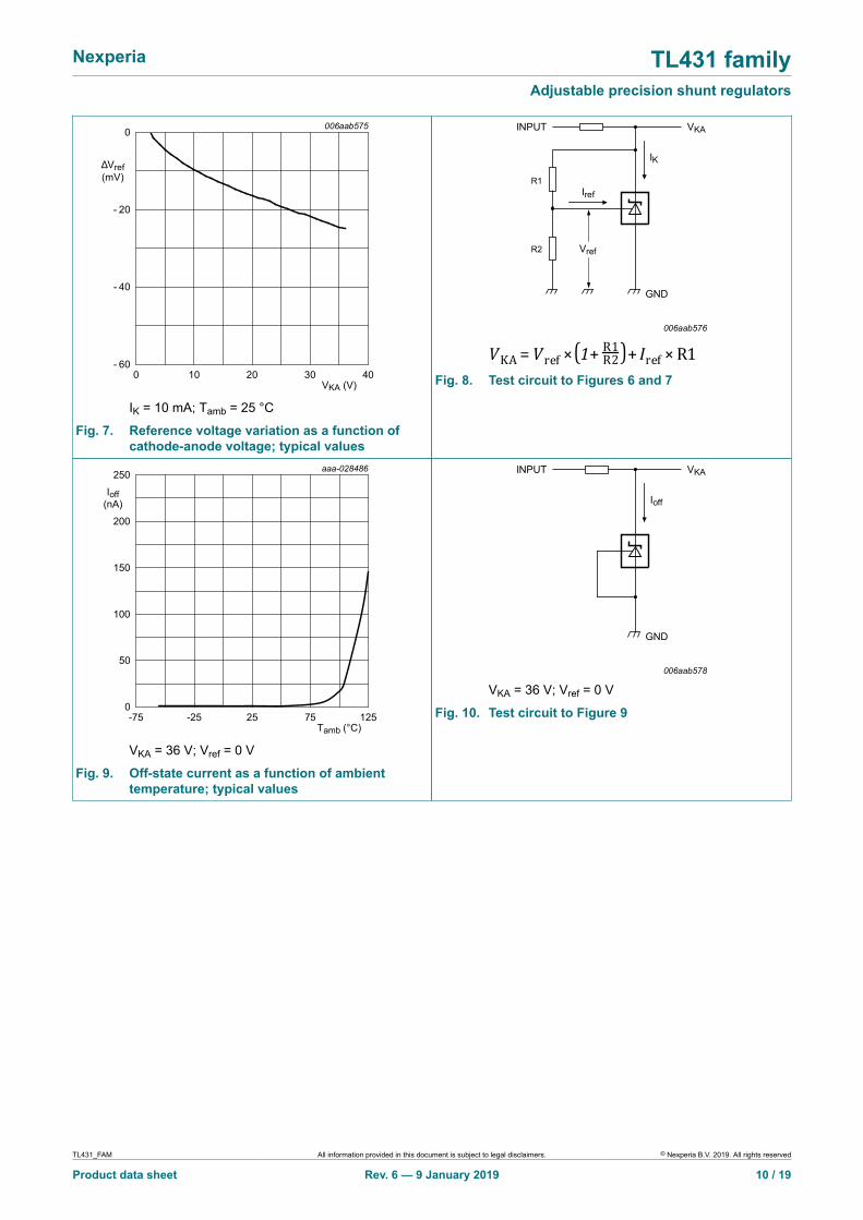
VKA (V)0 403010 20
006aab575
- 40
- 20
0
ΔVref (mV)
- 60
IK = 10 mA; Tamb = 25 °C
Fig. 7. Reference voltage variation as a function ofcathode-anode voltage; typical values
006aab576
GND
Vref
VKAINPUT
IK
IrefR1
R2
Fig. 8. Test circuit to Figures 6 and 7
Tamb (°C)-75 12575-25 25
aaa-028486
100
150
50
200
250
Ioff(nA)
0
VKA = 36 V; Vref = 0 V
Fig. 9. Off-state current as a function of ambienttemperature; typical values
006aab578
GND
VKAINPUT
Ioff
VKA = 36 V; Vref = 0 V
Fig. 10. Test circuit to Figure 9
TL431_FAM All information provided in this document is subject to legal disclaimers. © Nexperia B.V. 2019. All rights reserved
Product data sheet Rev. 6 — 9 January 2019 10 / 19
Nexperia TL431 familyAdjustable precision shunt regulators
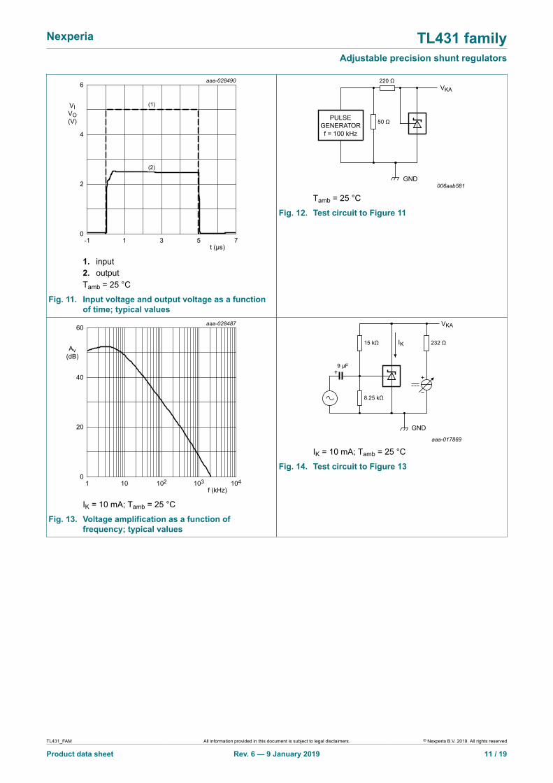
t (µs)-1 751 3
aaa-028490
2
4
6
VIVO(V)
0
(1)
(2)
1. input2. outputTamb = 25 °C
Fig. 11. Input voltage and output voltage as a functionof time; typical values
006aab581GND
VKA220 Ω
50 ΩPULSE GENERATOR f = 100 kHz
Tamb = 25 °C
Fig. 12. Test circuit to Figure 11
aaa-028487
20
40
60
Av(dB)
0
f (kHz)1 10410310 102
IK = 10 mA; Tamb = 25 °C
Fig. 13. Voltage amplification as a function offrequency; typical values
aaa-017869
GND
VKA
IK
9 µF
IK = 10 mA; Tamb = 25 °C
Fig. 14. Test circuit to Figure 13
TL431_FAM All information provided in this document is subject to legal disclaimers. © Nexperia B.V. 2019. All rights reserved
Product data sheet Rev. 6 — 9 January 2019 11 / 19
Nexperia TL431 familyAdjustable precision shunt regulators
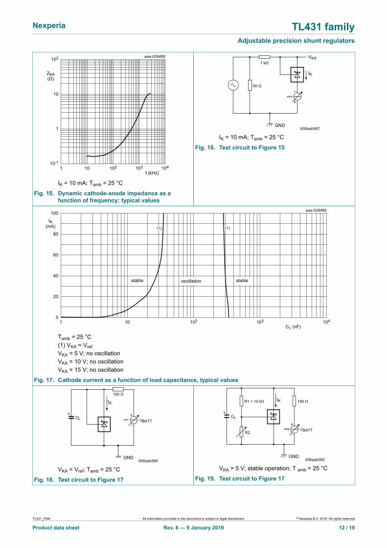
aaa-028488
10
1
102
ZKA(Ω)
10-1
f (kHz)1 10410310 102
IK = 10 mA; Tamb = 25 °C
Fig. 15. Dynamic cathode-anode impedance as afunction of frequency; typical values
006aab587GND
VKA
IK
50 Ω
1 kΩ
IK = 10 mA; Tamb = 25 °C
Fig. 16. Test circuit to Figure 15
aaa-028489
40
60
20
80
100
IK(mA)
0
CL (nF)1 10410310 102
(1) (1)
stable stableoscillation
Tamb = 25 °C(1) VKA = VrefVKA = 5 V; no oscillationVKA = 10 V; no oscillationVKA = 15 V; no oscillation
Fig. 17. Cathode current as a function of load capacitance, typical values
006aab589GND
CL
IK
150 Ω
VBATT
VKA = Vref; Tamb = 25 °C
Fig. 18. Test circuit to Figure 17
006aab590GND
CL
IK 150 Ω
VBATTR2
R1 = 10 kΩ
VKA > 5 V; stable operation; T amb = 25 °C
Fig. 19. Test circuit to Figure 17
TL431_FAM All information provided in this document is subject to legal disclaimers. © Nexperia B.V. 2019. All rights reserved
Product data sheet Rev. 6 — 9 January 2019 12 / 19
Nexperia TL431 familyAdjustable precision shunt regulators
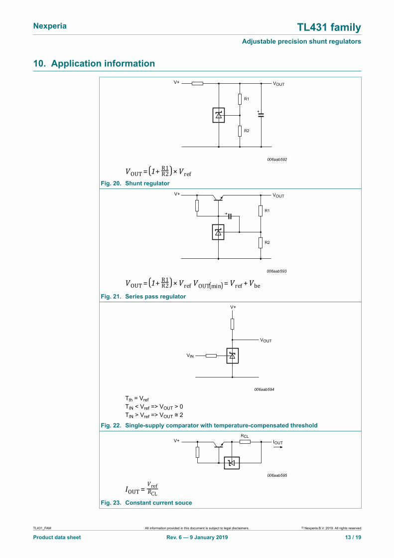
10. Application information
006aab592
VOUT
R1
R2
V+
Fig. 20. Shunt regulator
006aab593
VOUT
R1
R2
V+
Fig. 21. Series pass regulator
006aab594
VOUT
V+
VIN
Tth = VrefTIN < Vref => VOUT > 0TIN > Vref => VOUT ≅ 2
Fig. 22. Single-supply comparator with temperature-compensated threshold
006aab595
IOUT
RCLV+
Fig. 23. Constant current souce
TL431_FAM All information provided in this document is subject to legal disclaimers. © Nexperia B.V. 2019. All rights reserved
Product data sheet Rev. 6 — 9 January 2019 13 / 19
Nexperia TL431 familyAdjustable precision shunt regulators
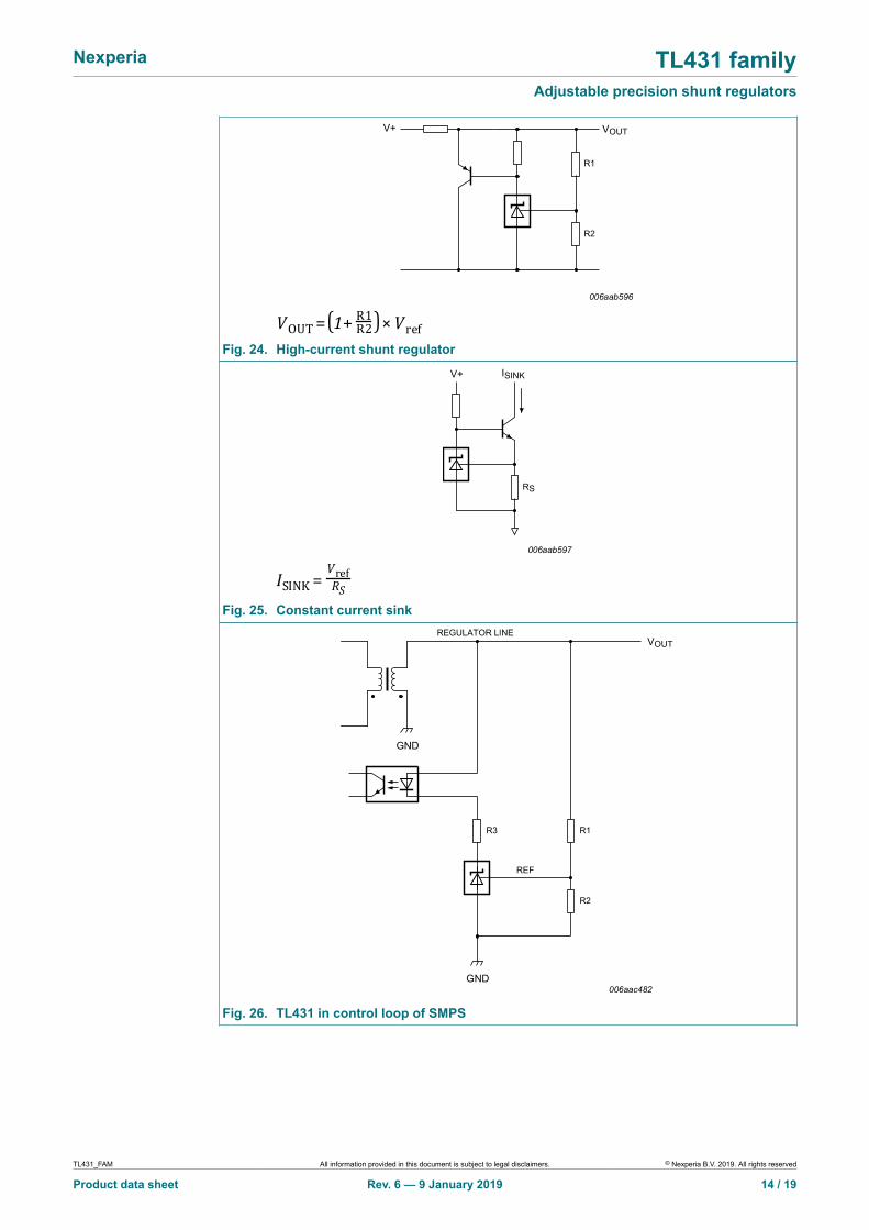
006aab596
VOUT
R1
R2
V+
Fig. 24. High-current shunt regulator
006aab597
ISINK
RS
V+
Fig. 25. Constant current sink
006aac482
VOUT
R1
R2
GND
R3
REF
GND
REGULATOR LINE
Fig. 26. TL431 in control loop of SMPS
TL431_FAM All information provided in this document is subject to legal disclaimers. © Nexperia B.V. 2019. All rights reserved
Product data sheet Rev. 6 — 9 January 2019 14 / 19
Nexperia TL431 familyAdjustable precision shunt regulators
11. Test information
Quality informationThis product has been qualified in accordance with the Automotive Electronics Council (AEC)standard Q100 - Failure mechanism based stress test qualification for integrated circuits, and issuitable for use in automotive applications.
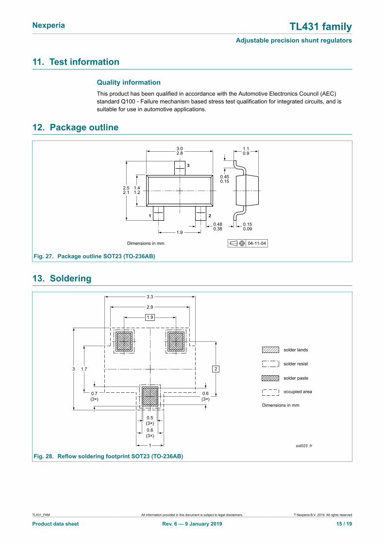
12. Package outline
04-11-04Dimensions in mm
0.45 0.15
1.9
1.1 0.9
3.0 2.8
2.5 2.1
1.4 1.2
0.48 0.38
0.15 0.09
1 2
3
Fig. 27. Package outline SOT23 (TO-236AB)
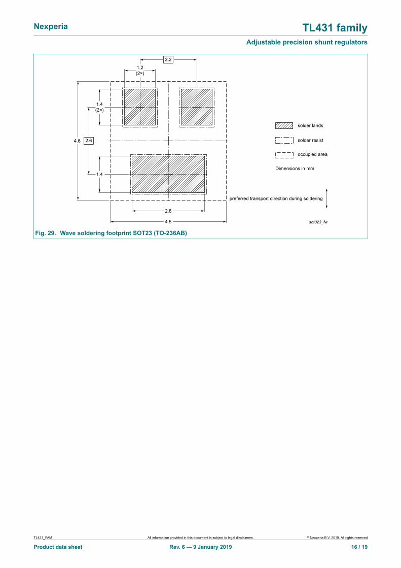
13. Soldering
solder lands
solder resist
occupied area
solder paste
sot023_fr
0.5 (3×)0.6 (3×)
0.6 (3×)
0.7 (3×)
3
1
3.3
2.9
1.7
1.9
2
Dimensions in mm
Fig. 28. Reflow soldering footprint SOT23 (TO-236AB)
TL431_FAM All information provided in this document is subject to legal disclaimers. © Nexperia B.V. 2019. All rights reserved
Product data sheet Rev. 6 — 9 January 2019 15 / 19
Nexperia TL431 familyAdjustable precision shunt regulators
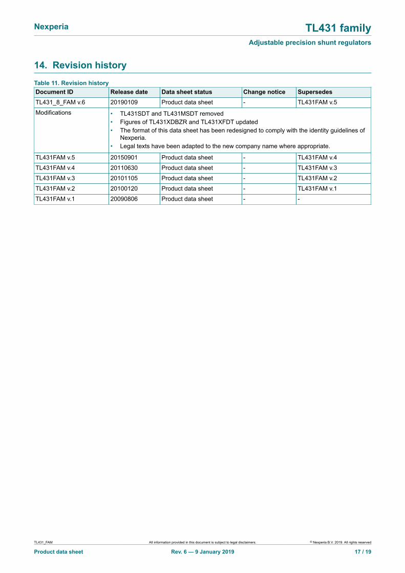
solder lands
solder resist
occupied area
preferred transport direction during soldering
sot023_fw
2.8
4.5
1.4
4.6
1.4 (2×)
1.2 (2×)
2.2
2.6
Dimensions in mm
Fig. 29. Wave soldering footprint SOT23 (TO-236AB)
TL431_FAM All information provided in this document is subject to legal disclaimers. © Nexperia B.V. 2019. All rights reserved
Product data sheet Rev. 6 — 9 January 2019 16 / 19
Nexperia TL431 familyAdjustable precision shunt regulators
14. Revision history
Table 11. Revision historyDocument ID Release date Data sheet status Change notice SupersedesTL431_8_FAM v.6 20190109 Product data sheet - TL431FAM v.5
Modifications • TL431SDT and TL431MSDT removed• Figures of TL431XDBZR and TL431XFDT updated• The format of this data sheet has been redesigned to comply with the identity guidelines of
Nexperia.• Legal texts have been adapted to the new company name where appropriate.
TL431FAM v.5 20150901 Product data sheet - TL431FAM v.4
TL431FAM v.4 20110630 Product data sheet - TL431FAM v.3
TL431FAM v.3 20101105 Product data sheet - TL431FAM v.2
TL431FAM v.2 20100120 Product data sheet - TL431FAM v.1
TL431FAM v.1 20090806 Product data sheet - -
TL431_FAM All information provided in this document is subject to legal disclaimers. © Nexperia B.V. 2019. All rights reserved
Product data sheet Rev. 6 — 9 January 2019 17 / 19
Nexperia TL431 familyAdjustable precision shunt regulators
15. Legal information
Data sheet status
Document status[1][2]
Productstatus [3]
Definition
Objective [short]data sheet
Development This document contains data fromthe objective specification forproduct development.
Preliminary [short]data sheet
Qualification This document contains data fromthe preliminary specification.
Product [short]data sheet
Production This document contains the productspecification.
[1] Please consult the most recently issued document before initiating orcompleting a design.
[2] The term 'short data sheet' is explained in section "Definitions".[3] The product status of device(s) described in this document may have
changed since this document was published and may differ in case ofmultiple devices. The latest product status information is available onthe internet at https://www.nexperia.com.
DefinitionsDraft — The document is a draft version only. The content is still underinternal review and subject to formal approval, which may result inmodifications or additions. Nexperia does not give any representations orwarranties as to the accuracy or completeness of information included hereinand shall have no liability for the consequences of use of such information.
Short data sheet — A short data sheet is an extract from a full data sheetwith the same product type number(s) and title. A short data sheet isintended for quick reference only and should not be relied upon to containdetailed and full information. For detailed and full information see the relevantfull data sheet, which is available on request via the local Nexperia salesoffice. In case of any inconsistency or conflict with the short data sheet, thefull data sheet shall prevail.
Product specification — The information and data provided in a Productdata sheet shall define the specification of the product as agreed betweenNexperia and its customer, unless Nexperia and customer have explicitlyagreed otherwise in writing. In no event however, shall an agreement bevalid in which the Nexperia product is deemed to offer functions and qualitiesbeyond those described in the Product data sheet.
DisclaimersLimited warranty and liability — Information in this document is believedto be accurate and reliable. However, Nexperia does not give anyrepresentations or warranties, expressed or implied, as to the accuracyor completeness of such information and shall have no liability for theconsequences of use of such information. Nexperia takes no responsibilityfor the content in this document if provided by an information source outsideof Nexperia.
In no event shall Nexperia be liable for any indirect, incidental, punitive,special or consequential damages (including - without limitation - lostprofits, lost savings, business interruption, costs related to the removalor replacement of any products or rework charges) whether or not suchdamages are based on tort (including negligence), warranty, breach ofcontract or any other legal theory.
Notwithstanding any damages that customer might incur for any reasonwhatsoever, Nexperia’s aggregate and cumulative liability towards customerfor the products described herein shall be limited in accordance with theTerms and conditions of commercial sale of Nexperia.
Right to make changes — Nexperia reserves the right to make changesto information published in this document, including without limitationspecifications and product descriptions, at any time and without notice. Thisdocument supersedes and replaces all information supplied prior to thepublication hereof.
Suitability for use in automotive applications — This Nexperia producthas been qualified for use in automotive applications. Unless otherwiseagreed in writing, the product is not designed, authorized or warranted tobe suitable for use in life support, life-critical or safety-critical systems or
equipment, nor in applications where failure or malfunction of an Nexperiaproduct can reasonably be expected to result in personal injury, death orsevere property or environmental damage. Nexperia and its suppliers acceptno liability for inclusion and/or use of Nexperia products in such equipment orapplications and therefore such inclusion and/or use is at the customer's ownrisk.
Quick reference data — The Quick reference data is an extract of theproduct data given in the Limiting values and Characteristics sections of thisdocument, and as such is not complete, exhaustive or legally binding.
Applications — Applications that are described herein for any of theseproducts are for illustrative purposes only. Nexperia makes no representationor warranty that such applications will be suitable for the specified usewithout further testing or modification.
Customers are responsible for the design and operation of their applicationsand products using Nexperia products, and Nexperia accepts no liability forany assistance with applications or customer product design. It is customer’ssole responsibility to determine whether the Nexperia product is suitableand fit for the customer’s applications and products planned, as well asfor the planned application and use of customer’s third party customer(s).Customers should provide appropriate design and operating safeguards tominimize the risks associated with their applications and products.
Nexperia does not accept any liability related to any default, damage, costsor problem which is based on any weakness or default in the customer’sapplications or products, or the application or use by customer’s third partycustomer(s). Customer is responsible for doing all necessary testing for thecustomer’s applications and products using Nexperia products in order toavoid a default of the applications and the products or of the application oruse by customer’s third party customer(s). Nexperia does not accept anyliability in this respect.
Limiting values — Stress above one or more limiting values (as defined inthe Absolute Maximum Ratings System of IEC 60134) will cause permanentdamage to the device. Limiting values are stress ratings only and (proper)operation of the device at these or any other conditions above thosegiven in the Recommended operating conditions section (if present) or theCharacteristics sections of this document is not warranted. Constant orrepeated exposure to limiting values will permanently and irreversibly affectthe quality and reliability of the device.
Terms and conditions of commercial sale — Nexperia products aresold subject to the general terms and conditions of commercial sale, aspublished at http://www.nexperia.com/profile/terms, unless otherwise agreedin a valid written individual agreement. In case an individual agreement isconcluded only the terms and conditions of the respective agreement shallapply. Nexperia hereby expressly objects to applying the customer’s generalterms and conditions with regard to the purchase of Nexperia products bycustomer.
No offer to sell or license — Nothing in this document may be interpretedor construed as an offer to sell products that is open for acceptance or thegrant, conveyance or implication of any license under any copyrights, patentsor other industrial or intellectual property rights.
Export control — This document as well as the item(s) described hereinmay be subject to export control regulations. Export might require a priorauthorization from competent authorities.
Translations — A non-English (translated) version of a document is forreference only. The English version shall prevail in case of any discrepancybetween the translated and English versions.
TrademarksNotice: All referenced brands, product names, service names andtrademarks are the property of their respective owners.
TL431_FAM All information provided in this document is subject to legal disclaimers. © Nexperia B.V. 2019. All rights reserved
Product data sheet Rev. 6 — 9 January 2019 18 / 19
Nexperia TL431 familyAdjustable precision shunt regulators
Contents
1. Product profile.............................................................. 11.1. General description......................................................11.2. Features and benefits..................................................11.3. Applications................................................................. 21.4. Quick reference data................................................... 22. Pinning information......................................................23. Ordering information....................................................34. Marking.......................................................................... 35. Functional diagram.......................................................46. Limiting values............................................................. 57. Recommended operating conditions..........................68. Thermal characteristics............................................... 69. Characteristics..............................................................710. Application information........................................... 1311. Test information........................................................1512. Package outline........................................................ 1513. Soldering................................................................... 1514. Revision history........................................................1715. Legal information......................................................18
© Nexperia B.V. 2019. All rights reservedFor more information, please visit: http://www.nexperia.comFor sales office addresses, please send an email to: [email protected] of release: 9 January 2019
TL431_FAM All information provided in this document is subject to legal disclaimers. © Nexperia B.V. 2019. All rights reserved
Product data sheet Rev. 6 — 9 January 2019 19 / 19