ads124x 24-bit, 2-ksps, analog-to-digital converters with ... · ads124x 24-bit, 2-ksps,...
TRANSCRIPT
AIN0/IEXC
AIN1/IEXC
BurnoutDetect
BurnoutDetect
3rd Orderû
Modulator
AVDD REFP1 REFN1 DVDD
ADS1247ADS1248
SCLK
DIN
DRDY
DOUT/DRDY
CS
START
RESET
DGNDCLKAVSS
InputMux
VBIAS
PGAAdjustable
DigitalFilter
SerialInterface
AndControl
Internal Oscillator
AIN2/IEXC/GPIO2
AIN3/IEXC/GPIO3
AIN4/IEXC/GPIO4
AIN5/IEXC/GPIO5
AIN6/IEXC/GPIO6
AIN7/IEXC/GPIO7
REFP0/GPIO0
REFN0/GPIO1
VREF Mux VoltageReference
GPIO
SystemMonitor
VREFOUT VREFCOM
IEXC1 IEXC2
ADS1248 Only
ADS1248 Only
DualIDACs
ADS1248 Only
AINP
AINN
BurnoutDetect
BurnoutDetect
3rd Orderû
Modulator
AVDD REFP REFN DVDD
ADS1246
SCLK
DIN
DRDY
DOUT/DRDY
CS
START
RESET
DGNDCLKAVSS
InputMux
VBIAS
PGAAdjustable
DigitalFilter
SerialInterface
AndControl
Internal Oscillator
Product
Folder
Sample &Buy
Technical
Documents
Tools &
Software
Support &Community
ReferenceDesign
An IMPORTANT NOTICE at the end of this data sheet addresses availability, warranty, changes, use in safety-critical applications,intellectual property matters and other important disclaimers. PRODUCTION DATA.
ADS1246, ADS1247, ADS1248SBAS426H –AUGUST 2008–REVISED MARCH 2016
ADS124x 24-Bit, 2-kSPS, Analog-To-Digital Converters WithProgrammable Gain Amplifier (PGA) For Sensor Measurement
1
1 Features1• Programmable Data Rates Up to 2 kSPS• Single-Cycle Settling for All Data Rates• Simultaneous 50-Hz and 60-Hz Rejection at 20
SPS• Analog Multiplexer With 8 (ADS1248) and 4
(ADS1247) Independently Selectable Inputs• Low-Noise PGA: 48 nVRMS at PGA = 128• Dual-Matched Programmable Excitation Current
Sources• Low-Drift Internal 2.048-V Reference:
10 ppm/°C (Maximum)• Sensor Burn-Out Detection• 4 or 8 General-Purpose I/Os (ADS1247,
ADS1248)• Internal Temperature Sensor• Power Supply and VREF Monitoring (ADS1247,
ADS1248)• Self and System Calibration• SPI™-Compatible Serial Interface• Analog Supply: Unipolar (2.7 V to 5.25 V) and
Bipolar (±2.5 V) Operation• Digital Supply: 2.7 V to 5.25 V
2 Applications• Temperature Sensor Measurements:
– RTDs, Thermocouples, and Thermistors• Pressure Measurements• Flow Meters• Factory Automation and Process Controls
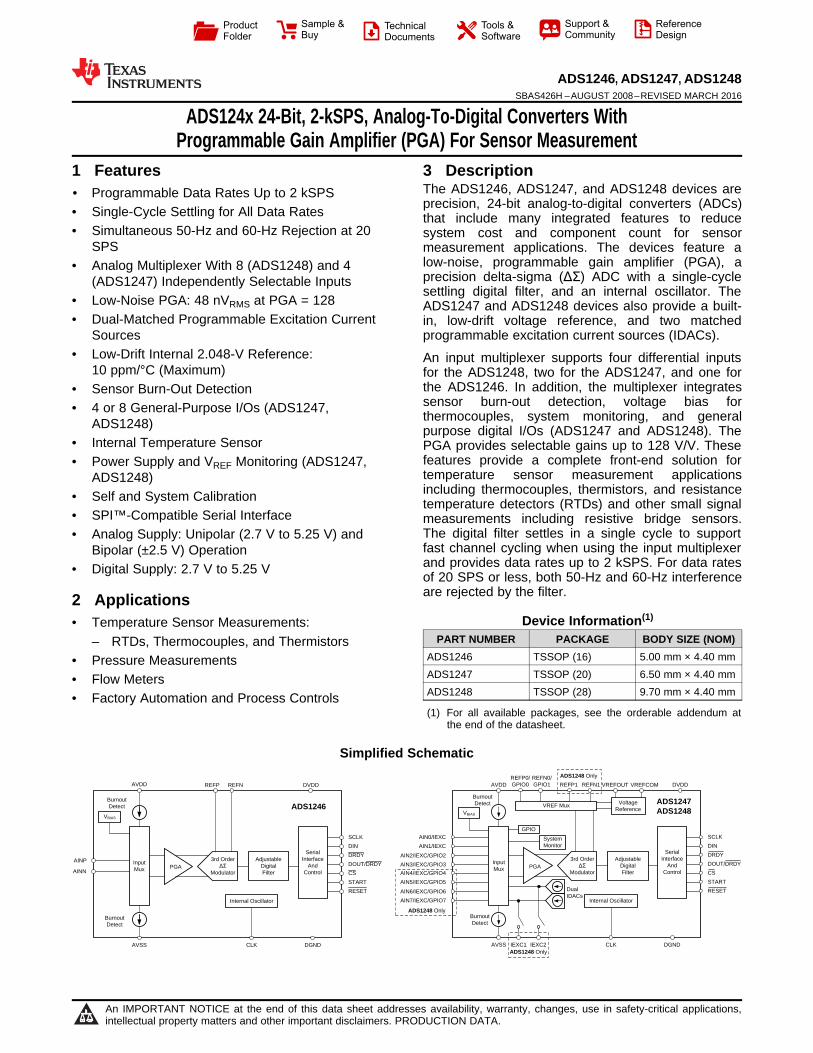
3 DescriptionThe ADS1246, ADS1247, and ADS1248 devices areprecision, 24-bit analog-to-digital converters (ADCs)that include many integrated features to reducesystem cost and component count for sensormeasurement applications. The devices feature alow-noise, programmable gain amplifier (PGA), aprecision delta-sigma (ΔΣ) ADC with a single-cyclesettling digital filter, and an internal oscillator. TheADS1247 and ADS1248 devices also provide a built-in, low-drift voltage reference, and two matchedprogrammable excitation current sources (IDACs).
An input multiplexer supports four differential inputsfor the ADS1248, two for the ADS1247, and one forthe ADS1246. In addition, the multiplexer integratessensor burn-out detection, voltage bias forthermocouples, system monitoring, and generalpurpose digital I/Os (ADS1247 and ADS1248). ThePGA provides selectable gains up to 128 V/V. Thesefeatures provide a complete front-end solution fortemperature sensor measurement applicationsincluding thermocouples, thermistors, and resistancetemperature detectors (RTDs) and other small signalmeasurements including resistive bridge sensors.The digital filter settles in a single cycle to supportfast channel cycling when using the input multiplexerand provides data rates up to 2 kSPS. For data ratesof 20 SPS or less, both 50-Hz and 60-Hz interferenceare rejected by the filter.
Device Information(1)
PART NUMBER PACKAGE BODY SIZE (NOM)ADS1246 TSSOP (16) 5.00 mm × 4.40 mmADS1247 TSSOP (20) 6.50 mm × 4.40 mmADS1248 TSSOP (28) 9.70 mm × 4.40 mm
(1) For all available packages, see the orderable addendum atthe end of the datasheet.
Simplified Schematic

2
ADS1246, ADS1247, ADS1248SBAS426H –AUGUST 2008–REVISED MARCH 2016 www.ti.com
Product Folder Links: ADS1246 ADS1247 ADS1248
Submit Documentation Feedback Copyright © 2008–2016, Texas Instruments Incorporated
Table of Contents1 Features .................................................................. 12 Applications ........................................................... 13 Description ............................................................. 14 Revision History..................................................... 25 Device Comparison Table ..................................... 46 Pin Configuration and Functions ......................... 57 Specifications......................................................... 7
7.1 Absolute Maximum Ratings ...................................... 77.2 ESD Ratings.............................................................. 77.3 Recommended Operating Conditions....................... 87.4 Thermal Information .................................................. 87.5 Electrical Characteristics........................................... 97.6 Timing Requirements .............................................. 117.7 Switching Characteristics ........................................ 117.8 Typical Characteristics ............................................ 13
8 Parameter Measurement Information ................ 218.1 Noise Performance ................................................. 21
9 Detailed Description ............................................ 249.1 Overview ................................................................. 249.2 Functional Block Diagram ....................................... 249.3 Feature Description................................................. 25
9.4 Device Functional Modes........................................ 369.5 Programming........................................................... 419.6 Register Maps ......................................................... 50
10 Application and Implementation........................ 7010.1 Application Information.......................................... 7010.2 Typical Applications .............................................. 7610.3 Do's and Don'ts..................................................... 86
11 Power-Supply Recommendations ..................... 8811.1 Power-Supply Sequencing.................................... 8811.2 Power-Supply Decoupling..................................... 88
12 Layout................................................................... 8912.1 Layout Guidelines ................................................. 8912.2 Layout Example .................................................... 90
13 Device and Documentation Support ................. 9113.1 Documentation Support ........................................ 9113.2 Related Links ........................................................ 9113.3 Community Resources.......................................... 9113.4 Trademarks ........................................................... 9113.5 Electrostatic Discharge Caution............................ 9113.6 Glossary ................................................................ 91
14 Mechanical, Packaging, and OrderableInformation ........................................................... 91
4 Revision HistoryNOTE: Page numbers for previous revisions may differ from page numbers in the current version.
Changes from Revision G (October 2011) to Revision H Page
• Added ESD Ratings table, Feature Description section, Device Functional Modes, Application and Implementationsection, Power Supply Recommendations section, Layout section, Device and Documentation Support section, andMechanical, Packaging, and Orderable Information section .................................................................................................. 1
• Updated Features and Description sections to include use in applications other than temperature measurement .............. 1• Edited Device Comparison Table to include ADS1146, ADS1147, and ADS1148; changed title, deleted footnote ............. 4• Merged all Pin Functions into one table, changed IOUT1 and IOUT2 to IEXC1 and IEXC2 to match figures...................... 6• Changed compliance voltage for excitation current sources in Electrical Characteristics, now refers to Figure 41 and
Figure 42; changed initial error and initial mismatch to absolute error and absolute mismatch ............................................ 9• Re-ordered elements in Timing Requirements tables, changed timing references to tCLK................................................... 11• Changed order of Typical Characteristics curves to match order in Electrical Characteristics table ................................... 13• Added cross-reference for Equation 1 in Noise Performance section ................................................................................. 21• Corrected values in Table 2.................................................................................................................................................. 22• Modified Low-Noise PGA section to add more detail; added Table 7; added PGA Common-Mode Voltage
Requirements and PGA Common-Mode Voltage Calculation Example sections ................................................................ 26• Added fCLK/fMOD column to Table 9 ....................................................................................................................................... 30• Added cross-reference for Equation 15 to Power-Supply Monitor section........................................................................... 35• Added cross-reference for Equation 16 to External Voltage Reference Monitor section..................................................... 35• Added Device Functional Modes section ............................................................................................................................. 36• Corrected values in Table 15 to remove extra 0 in 800000h ............................................................................................... 40• Added text to Chip Select section to say that SCLK will force DRDY high, even with CS high........................................... 41• Added text to Data Output and Data Ready section to say that stop read data continuous mode is not compatible
with DRDY MODE set to 1 ................................................................................................................................................... 42• Modified Figure 74 and Figure 75 to better show DIN transitions with respect to SCLK; replaced Figure 76 to better

3
ADS1246, ADS1247, ADS1248www.ti.com SBAS426H –AUGUST 2008–REVISED MARCH 2016
Product Folder Links: ADS1246 ADS1247 ADS1248
Submit Documentation FeedbackCopyright © 2008–2016, Texas Instruments Incorporated
Revision History (continued)show full command and DRDY/DOUT falling with NOP....................................................................................................... 43
• Added more infomation to Data Format section; added Figure 77 ...................................................................................... 44• Added cross-reference for Figure 78 to Commands section................................................................................................ 45• Modified Figure 78 to include CS status through SLEEP and WAKEUP command ............................................................ 46• Updated Figure 79 and Figure 80 to show start of command execution ............................................................................. 46• Added cross-reference for Figure 83 to Commands section................................................................................................ 47• Removed figure for SDATAC (Stop Read Data Continuous) command .............................................................................. 47• Updated Figure 85 to show MUX1 as the start of the data byte for the given command and register location................... 48• Updated Figure 86 to show start of calibration timing .......................................................................................................... 49• Updated Register Maps section to new format .................................................................................................................... 50• Updated Application Information section. Included new typical applications for Ratiometric 3-Wire RTD
Measurement System and K-Type Thermocouple Measurement (–200°C to +1250°C) with Cold-JunctionCompensation....................................................................................................................................................................... 70
• Updated Figure 112 and Figure 113 to better show timing information ............................................................................... 74• Removed Hardware-Compensated 3-Wire RTD Measurement application section ............................................................ 76
Changes from Revision F (June 2011) to Revision G Page
• Added Figure 35 .................................................................................................................................................................. 17• Added Figure 41 and Figure 42............................................................................................................................................ 18
Changes from Revision E (December, 2010) to Revision F Page
• Added footnote to Full-scale input voltage specification in Electrical Characteristics table ................................................... 8• Added test condition for INL parameter of Electrical Characteristics ..................................................................................... 9• Added tCSPW to minimum specification in Timing Characteristics for Figure 1...................................................................... 11• Updated Figure 1 to show tCSPW timing ................................................................................................................................ 12• Corrected grid and axis values for Figure 29 ....................................................................................................................... 16• Corrected grid and axis values for Figure 30 ....................................................................................................................... 16• Updated Figure 51................................................................................................................................................................ 25• Added details to Bias Voltage Generation section ............................................................................................................... 34• Corrected Table 14............................................................................................................................................................... 39• Added details to Calibration section ..................................................................................................................................... 39• Added Equation 18 to Calibration section ............................................................................................................................ 39• Added section to Calibration Commands ............................................................................................................................. 40• Added details to Digital Interface section ............................................................................................................................. 43• Added Restricted command space to Table 19 ................................................................................................................... 45

4
ADS1246, ADS1247, ADS1248SBAS426H –AUGUST 2008–REVISED MARCH 2016 www.ti.com
Product Folder Links: ADS1246 ADS1247 ADS1248
Submit Documentation Feedback Copyright © 2008–2016, Texas Instruments Incorporated
5 Device Comparison Table
PRODUCT RESOLUTION (Bits) NUMBER OFINPUTS
VOLTAGEREFERENCE
EXCITATIONCURRENTSOURCES
PACKAGE
ADS1146 16 1 Differential External No TSSOP-16ADS1147 16 4-Input Multiplexer Internal or External Yes TSSOP-20
ADS1148 16 8-Input Multiplexer Internal or External Yes TSSOP-28VQFN-32
ADS1246 24 1 Differential External No TSSOP-16ADS1247 24 4-Input Multiplexer Internal or External Yes TSSOP-20ADS1248 24 8-Input Multiplexer Internal or External Yes TSSOP-28

DVDD
DGND
CLK
RESET
REFP
REFN
AINP
AINN
SCLK
DIN
DOUT/DRDY
DRDY
CS
START
AVDD
AVSS
1
2
3
4
5
6
7
8
16
15
14
13
12
11
10
9
ADS1246
DVDD
DGND
CLK
RESET
REFP0/GPIO0
REFN0/GPIO1
REFP1
REFN1
VREFOUT
VREFCOM
AIN0/IEXC
AIN1/IEXC
AIN4/IEXC/GPIO4
AIN5/IEXC/GPIO5
SCLK
DIN
DOUT/DRDY
DRDY
CS
START
AVDD
AVSS
IEXC1
IEXC2
AIN3/IEXC/GPIO3
AIN2/IEXC/GPIO2
AIN7/IEXC/GPIO7
AIN6/IEXC/GPIO6
1
2
3
4
5
6
7
8
9
10
11
12
13
14
28
27
26
25
24
23
22
21
20
19
18
17
16
15
ADS1248
DVDD
DGND
CLK
RESET
REFP0/GPIO0
REFN0/GPIO1
VREFOUT
VREFCOM
AIN0/IEXC
AIN1/IEXC
SCLK
DIN
DOUT/DRDY
DRDY
CS
START
AVDD
AVSS
AIN3/IEXC/GPIO3
AIN2/IEXC/GPIO2
1
2
3
4
5
6
7
8
9
10
20
19
18
17
16
15
14
13
12
11
ADS1247
5
ADS1246, ADS1247, ADS1248www.ti.com SBAS426H –AUGUST 2008–REVISED MARCH 2016
Product Folder Links: ADS1246 ADS1247 ADS1248
Submit Documentation FeedbackCopyright © 2008–2016, Texas Instruments Incorporated
6 Pin Configuration and Functions
PW Package28-Pin TSSOP
Top ViewPW Package
20-Pin TSSOPTop View
PW Package16-Pin TSSOP
Top View

6
ADS1246, ADS1247, ADS1248SBAS426H –AUGUST 2008–REVISED MARCH 2016 www.ti.com
Product Folder Links: ADS1246 ADS1247 ADS1248
Submit Documentation Feedback Copyright © 2008–2016, Texas Instruments Incorporated
(1) G = Ground, I = Input, O = Output, P = Power(2) See Unused Inputs and Outputs for unused pin connections.
Pin FunctionsPIN
TYPE (1) DESCRIPTION (2)
NAME ADS1248(TSSOP-28)
ADS1247(TSSOP-20)
ADS1246(TSSOP-16)
AIN0/IEXC 11 9 — I Analog input 0, optional excitation current output
AIN1/IEXC 12 10 — I Analog input 1, optional excitation current output
AIN2/IEXC/GPIO2 17 11 — I/O Analog input 2, optional excitation current output,or general-purpose digital input/output pin 2
AIN3/IEXC/GPIO3 18 12 — I/O Analog input 3, optional excitation current output,or general-purpose digital input/output pin 3
AIN4/IEXC/GPIO4 13 — — I/O Analog input 4, optional excitation current output,or general-purpose digital input/output pin 4
AIN5/IEXC/GPIO5 14 — — I/O Analog input 5, optional excitation current output,or general-purpose digital input/output pin 5
AIN6/IEXC/GPIO6 15 — — I/O Analog input 6, optional excitation current output,or general-purpose digital input/output pin 6
AIN7/IEXC/GPIO7 16 — — I/O Analog input 7, optional excitation current output,or general-purpose digital input/output pin 7
AINN — — 8 I Negative analog input
AINP — — 7 I Positive analog input
AVDD 22 14 10 P Positive analog power supply, connect a 0.1-μF capacitor toAVSS
AVSS 21 13 9 P Negative analog power supply
CLK 3 3 3 I External clock input, tie to DGND to activate the internaloscillator
CS 24 16 12 I Chip select (active low)
DGND 2 2 2 G Digital ground
DIN 27 19 15 I Serial data input
DOUT/DRDY 26 18 14 O Serial data output or data output combined with data ready
DRDY 25 17 13 O Data ready (active low)
DVDD 1 1 1 P Digital power supply, connect a 0.1-μF capacitor to DGND
IEXC1 20 — — O Excitation current output 1
IEXC2 19 — — O Excitation current output 2
REFN — — 6 I Negative external reference input
REFN0/GPIO1 6 6 — I/O Negative external reference input 0, orgeneral-purpose digital input/output pin 1
REFN1 8 — — I Negative external reference input 1
REFP — — 5 I Positive external reference input
REFP0/GPIO0 5 5 — I/O Positive external reference input 0, orgeneral-purpose digital input/output pin 0
REFP1 7 — — I Positive external reference input 1
RESET 4 4 4 I Reset (active low)
SCLK 28 20 16 I Serial clock input
START 23 15 11 I Conversion start
VREFCOM 10 8 — ONegative internal reference voltage output, connect to AVSSwhen using a unipolar supply or to the mid-voltage of thepower supply when using a bipolar supply
VREFOUT 9 7 — O Positive internal reference voltage output, connect a capacitorin the range of 1-μF to 47-μF to VREFCOM

7
ADS1246, ADS1247, ADS1248www.ti.com SBAS426H –AUGUST 2008–REVISED MARCH 2016
Product Folder Links: ADS1246 ADS1247 ADS1248
Submit Documentation FeedbackCopyright © 2008–2016, Texas Instruments Incorporated
(1) Stresses beyond those listed under Absolute Maximum Ratings may cause permanent damage to the device. These are stress ratingsonly, which do not imply functional operation of the device at these or any other conditions beyond those indicated under RecommendedOperating Conditions. Exposure to absolute-maximum-rated conditions for extended periods may affect device reliability.
7 Specifications
7.1 Absolute Maximum Ratings (1)
MIN MAX UNIT
Power-supply voltageAVDD to AVSS –0.3 5.5
VAVSS to DGND –2.8 0.3DVDD to DGND –0.3 5.5
Analog input voltage AINx, REFPx, REFNx, VREFOUT, VREFCOM, IEXC1, IEXC2 AVSS – 0.3 AVDD + 0.3 VDigital input voltage SCLK, DIN, DOUT/DRDY, DRDY, CS, START, RESET, CLK DGND – 0.3 DVDD + 0.3 V
Input currentContinuous, any pin except power supply pins –10 10
mAMomentary, any pin except power supply pins –100 100
TemperatureJunction, TJ 150
°CStorage, Tstg –60 150
(1) JEDEC document JEP155 states that 500-V HBM allows safe manufacturing with a standard ESD control process.(2) JEDEC document JEP157 states that 250-V CDM allows safe manufacturing with a standard ESD control process.
7.2 ESD RatingsVALUE UNIT
V(ESD) Electrostatic dischargeHuman body model (HBM), per ANSI/ESDA/JEDEC JS-001, all pins (1) ±2000
VCharged device model (CDM), per JEDEC specification JESD22-C101,all pins (2) ±500

8
ADS1246, ADS1247, ADS1248SBAS426H –AUGUST 2008–REVISED MARCH 2016 www.ti.com
Product Folder Links: ADS1246 ADS1247 ADS1248
Submit Documentation Feedback Copyright © 2008–2016, Texas Instruments Incorporated
(1) AINP and AINN denote the positive and negative inputs of the PGA.(2) For VREF > 2.7 V, the differential input voltage must not exceed 2.7 V / Gain.(3) REFPx and REFNx denote the differential reference input pair (ADS1246, ADS1247), or one of the two available differential reference
input pairs (ADS1248).(4) External clock only required if the internal oscillator is not used.
7.3 Recommended Operating ConditionsOver operating ambient temperature range (unless otherwise noted)
MIN NOM MAX UNIT
POWER SUPPLY
Analog power supply
AVDD to AVSS 2.7 5.25
VAVSS to DGND –2.65 0.1
AVDD to DGND 2.25 5.25
Digital power supply DVDD to DGND 2.7 5.25 V
ANALOG INPUTS (1)
VIN Differential input voltage V(AINP) – V(AINN)(2) –VREF / Gain VREF / Gain V
VCM Common-mode input voltage (V(AINP) + V(AINN)) / 2 See Equation 3 V
VOLTAGE REFERENCE INPUTS (3)
VREF Differential reference input voltage V(REFPx) – V(REFNx) 0.5 (AVDD – AVSS) – 1 V
V(REFNx) Absolute negative reference voltage AVSS – 0.1 V(REFPx) – 0.5 V
V(REFPx) Absolute positive reference voltage V(REFNx) + 0.5 AVDD + 0.1 V
EXTERNAL CLOCK INPUT (4)
fCLK External clock frequency 1 4.5 MHz
External clock duty cycle 25% 75%
GENERAL-PURPOSE INPUTS/OUTPUTS (GPIO)
GPIO input voltage AVSS AVDD V
DIGITAL INPUTS
Digital input voltage DGND DVDD V
TEMPERATURE RANGE
TA Operating ambient temperature –40 125 °C
Specified ambient temperature –40 105 °C
(1) For more information about traditional and new thermal metrics, see the Semiconductor and IC Package Thermal Metrics applicationreport, SPRA953.
7.4 Thermal Information
THERMAL METRIC (1)ADS1246 ADS1247 ADS1248
UNITPW (TSSOP) PW (TSSOP) PW (TSSOP)16 PINS 20 PINS 28 PINS
RθJA Junction-to-ambient thermal resistance 95.2 87.6 54.6 °C/WRθJC(top) Junction-to-case (top) thermal resistance 28.8 21.2 11.3 °C/WRθJB Junction-to-board thermal resistance 41.1 39.9 13 °C/WψJT Junction-to-top characterization parameter 1.5 0.8 0.5 °C/WψJB Junction-to-board characterization parameter 40.4 39.2 12.7 °C/WRθJC(bot) Junction-to-case (bottom) thermal resistance n/a n/a n/a °C/W

9
ADS1246, ADS1247, ADS1248www.ti.com SBAS426H –AUGUST 2008–REVISED MARCH 2016
Product Folder Links: ADS1246 ADS1247 ADS1248
Submit Documentation FeedbackCopyright © 2008–2016, Texas Instruments Incorporated
(1) Offset calibration on the order of noise.(2) Specified by the combination of design and final production test.(3) Do not exceed this loading on the internal voltage reference.
7.5 Electrical CharacteristicsMinimum and maximum specifications apply from TA = –40°C to 105°C. Typical specifications are at TA = 25°C.All specifications are at AVDD = 5 V, DVDD = 3.3 V, AVSS = 0 V, external VREF = 2.048 V, and fCLK = 4.096 MHz (unlessotherwise noted).
PARAMETER TEST CONDITIONS MIN TYP MAX UNIT
ANALOG INPUTS
Differential input current 100 pA
Absolute input current See Table 8
PGA
PGA gain settings 1, 2, 4, 8, 16, 32, 64, 128 V/V
SYSTEM PERFORMANCE
Resolution 24 Bits
DR Data rate 5, 10, 20, 40, 80, 160, 320, 640, 1000, 2000 SPS
ADC conversion time Single-cycle settling
INL Integral nonlinearity Differential input, end point fit,Gain = 1, VCM = 2.5 V 6 15 ppm
VIO Offset voltage (input referred) After calibration (1) –15 15 μV
Offset drift See Figure 9 to Figure 12
Gain error TA = 25°C, all Gains,DR = 40 SPS, 80 SPS, or 160 SPS –0.02% ±0.005% 0.02%
Gain drift See Figure 17 to Figure 20
Noise See Table 1 to Table 4
NMRR Normal-mode rejection See Table 10
CMRR Common-mode rejectionAt DC, Gain = 1 80 90
dBAt DC, Gain = 32 90 125
PSRR Power-supply rejection AVDD / DVDD at DC,Gain = 32, DR = 80 SPS 100 135 dB
VOLTAGE REFERENCE INPUTS
Reference input current 30 nA
INTERNAL VOLTAGE REFERENCE
VREF Internal reference voltage 2.038 2.048 2.058 V
Reference drift (2) TA = 25°C to 105°C 2 10 ppm/°C
TA = –40°C to 105°C 6 15 ppm/°C
Output current (3) –10 10 mA
Load regulation 50 μV/mA
Start-up time See Table 11
INTERNAL OSCILLATOR
Internal oscillator frequency 3.89 4.096 4.3 MHz
EXCITATION CURRENT SOURCES (IDACs)
Output current settings 50, 100, 250, 500, 750, 1000, 1500 μA
Compliance voltage All currents See Figure 41 and Figure 42
Absolute error All currents, each IDAC –6% ±1% 6%
Absolute mismatch All currents, between IDACs ±0.15%
Temperature drift Each IDAC 100 ppm/°C
Temperature drift matching Between IDACs 10 ppm/°C
BURN-OUT CURRENT SOURCES
Burn-out current source settings 0.5, 2, 10 μA

10
ADS1246, ADS1247, ADS1248SBAS426H –AUGUST 2008–REVISED MARCH 2016 www.ti.com
Product Folder Links: ADS1246 ADS1247 ADS1248
Submit Documentation Feedback Copyright © 2008–2016, Texas Instruments Incorporated
Electrical Characteristics (continued)Minimum and maximum specifications apply from TA = –40°C to 105°C. Typical specifications are at TA = 25°C.All specifications are at AVDD = 5 V, DVDD = 3.3 V, AVSS = 0 V, external VREF = 2.048 V, and fCLK = 4.096 MHz (unlessotherwise noted).
PARAMETER TEST CONDITIONS MIN TYP MAX UNIT
BIAS VOLTAGE
Bias voltage (AVDD + AVSS) / 2 V
Bias voltage output impedance 400 Ω
TEMPERATURE SENSOR
Output voltage TA = 25°C 118 mV
Temperature coefficient 405 μV/°C
GENERAL-PURPOSE INPUTS/OUTPUTS (GPIO)
VIL Low-level input voltage AVSS 0.3 × AVDD V
VIH High-level input voltage 0.7 × AVDD AVDD V
VOL Low-level output voltage IOL = 1 mA 0.2 × AVDD V
VOH High-level output voltage IOH = 1 mA 0.8 × AVDD V
DIGITAL INPUTS/OUTPUTS (other than GPIO)
VIL Low-level input voltage DGND 0.3 × DVDD V
VIH High-level input voltage 0.7 × DVDD DVDD V
VOL Low-level output voltage IOL = 1 mA DGND 0.2 × DVDD V
VOH High-level output voltage IOH = 1 mA 0.8 × DVDD V
Input leakage DGND < VIN < DVDD –10 10 μA
POWER SUPPLY
IAVDD Analog supply current
Power-down mode 0.1
µA
Converting, AVDD = 3.3 V,DR = 20 SPS, external reference 200
Converting, AVDD = 5 V,DR = 20 SPS, external reference 225
Additional current with internal referenceenabled 180
IDVDD Digital supply current
Power-down mode 0.2
μANormal operation, DVDD = 3.3 V,DR = 20 SPS, internal oscillator 210
Normal operation, DVDD = 5 V,DR = 20 SPS, internal oscillator 230
PD Power dissipation
AVDD = DVDD = 5 V,DR = 20 SPS, internal oscillator, externalreference
2.3
mWAVDD = DVDD = 3.3 V,DR = 20 SPS, internal oscillator, externalreference
1.4

11
ADS1246, ADS1247, ADS1248www.ti.com SBAS426H –AUGUST 2008–REVISED MARCH 2016
Product Folder Links: ADS1246 ADS1247 ADS1248
Submit Documentation FeedbackCopyright © 2008–2016, Texas Instruments Incorporated
(1) tCLK = 1 / fCLK. The default clock frequency fCLK = 4.096 MHz.(2) Applicable only when fCLK = 4.096 MHz, scales proportionally with fCLK frequency.
7.6 Timing RequirementsAt TA = –40°C to 105°C and DVDD = 2.7 V to 5.5 V (unless otherwise noted)
PARAMETER MIN NOM MAX UNITSERIAL INTERFACE (SEE Figure 1 AND Figure 2)tCSSC Delay time, First SCLK rising edge after CS falling edge 10 nstSCCS Delay time, CS rising edge after final SCLK falling edge 7 tCLK
(1)
tCSPW Pulse duration, CS high 5 tCLK
tSCLK SCLK period488 ns
64 ConversionstSPWH Pulse duration, SCLK high 0.25 0.75 tSCLK
tSPWL Pulse duration, SCLK low 0.25 0.75 tSCLK
tDIST Setup time, DIN valid before SCLK falling edge 5 nstDIHD Hold time, DIN valid after SCLK falling edge 5 nstSTD Setup time, SCLK low before DRDY rising edge 5 tCLK
tDTS Delay time, SCLK rising edge after DRDY falling edge 1 tCLK
MINIMUM START TIME PULSE DURATION (SEE Figure 3)tSTART Pulse duration, START high 3 tCLK
RESET PULSE DURATION, SERIAL INTERFACE COMMUNICATION AFTER RESET (SEE Figure 4)tRESET Pulse duration, RESET low 4 tCLK
tRHSCDelay time, SCLK rising edge (start of serial interface communication)after RESET rising edge 0.6 (2) ms
7.7 Switching CharacteristicsAt TA = –40°C to 105°C and DVDD = 2.7 V to 5.5 V (unless otherwise noted; see Figure 1 and Figure 2)
PARAMETER TEST CONDITIONS MIN TYP MAX UNIT
tDOPDPropagation delay time,SCLK rising edge to valid new DOUT
DVDD ≤ 3.6 V 50ns
DVDD > 3.6 V 180tDOHD DOUT hold time 0 ns
tCSDOPropagation delay time,CS rising edge to DOUT high impedance 10 ns
tPWH Pulse duration, DRDY high 3 tCLK

SCLK
CS
RESET
tRESET
tRHSC
tSTARTSTART
1 42 3 5 6 7 8
SCLK(2)
DRDY
tDTS
tPWH
tSTD(1)
SCLK
DOUT/DRDY
DIN DIN[4]
CS
DIN[5]DIN[6]DIN[7]DIN[0]
DOUT[7] DOUT[6] DOUT[5] DOUT[4]
DIN[0]DIN[1]
DOUT[1] DOUT[0]
tCSSC
tDIST tDIHD
tSCLK tSPWH
tSPWL
tSCCS
tCSPW
tCSDO
tDOHDtDOPD
12
ADS1246, ADS1247, ADS1248SBAS426H –AUGUST 2008–REVISED MARCH 2016 www.ti.com
Product Folder Links: ADS1246 ADS1247 ADS1248
Submit Documentation Feedback Copyright © 2008–2016, Texas Instruments Incorporated
Figure 1. Serial Interface Timing, DRDY MODE Bit = 0
(1) This timing diagram is applicable only when the CS pin is low. SCLK does not need to be low during tSTD when CS ishigh.
(2) SCLK must only be sent in multiples of eight during partial retrieval of output data.
Figure 2. Serial Interface Timing to Allow Conversion Result Loading
Figure 3. Minimum Start Pulse Duration
Figure 4. Reset Pulse Duration and Serial Interface Communication After Reset

4
3
2
1
0
-1
-2
-3
Temperature ( C)°
Input-
Refe
rred O
ffset (
V)
m
-40 -20 0 20 40 60 80 100 120
PGA = 32
PGA = 1
PGA = 128
AVDD = 5V
Data Rate = 20SPS
8
6
4
2
0
-2
-4
-6
-8
Temperature ( C)°
Inp
ut-
Re
ferr
ed
Off
se
t (
V)
m
-40 -20 0 20 40 60 80 100 120
PGA = 32
PGA = 1
PGA = 128
AVDD = 5V
Data Rate = 160SPS
8
6
4
2
0
-2
-4
-6
-8
V (% of FSR)IN
INL (
ppm
of F
SR
)
-100 -50 0 50 100
PGA = 128
Data Rate = 20SPS
-40°C
+25 C°
+105 C°
-10°C
8
6
4
2
0
-2
-4
-6
-8
V (% of FSR)IN
INL (
ppm
of F
SR
)
-100 -50 0 50 100
PGA = 1
Data Rate = 2kSPS
- °40 C
+25 C°
+105 C°
- °10 C
8
6
4
2
0
-2
-4
-6
-8
V (% of FSR)IN
INL (
ppm
of F
SR
)
-100 -50 0 50 100
PGA = 1
Data Rate = 20SPS
- °40 C
- °10 C
+25 C°
+105 C°
8
6
4
2
0
-2
-4
-6
-8
-10
V (% of FSR)IN
INL (
ppm
of F
SR
)
-100 -50 0 50 100
PGA = 32
Data Rate = 20SPS
- °40 C
+25 C°
+105 C°
- °10 C
13
ADS1246, ADS1247, ADS1248www.ti.com SBAS426H –AUGUST 2008–REVISED MARCH 2016
Product Folder Links: ADS1246 ADS1247 ADS1248
Submit Documentation FeedbackCopyright © 2008–2016, Texas Instruments Incorporated
7.8 Typical CharacteristicsAt TA = 25°C, AVDD = 5 V, AVSS = 0 V, and external VREF = 2.5 V (unless otherwise noted)
Figure 5. Integral Nonlinearity vs Input Signal Figure 6. Integral Nonlinearity vs Input Signal
Figure 7. Integral Nonlinearity vs Input Signal Figure 8. Integral Nonlinearity vs Input Signal
Figure 9. Offset vs Temperature Figure 10. Offset vs Temperature

10
8
6
4
2
0
2
4
6
8
-
-
-
-
Temperature ( C)°
Inp
ut-
Re
ferr
ed
Off
se
t (
V)
m
-40 -20 0 20 40 60 80 100 120
AVDD = 3.3V
Data Rate = 640SPS
PGA = 1
PGA = 32
PGA = 128
8
6
4
2
0
2
4
6
-
-
-
Temperature ( C)°
Inp
ut-
Re
ferr
ed
Off
se
t (
V)
m
-40 -20 0 20 40 60 80 100 120
AVDD = 3.3V
Data Rate = 2kSPS
PGA = 1
PGA = 32
PGA = 128
4
3
2
1
0
1
2
3
-
-
-
Temperature ( C)°
Inp
ut-
Re
ferr
ed
Off
se
t (
V)
m
-40 -20 0 20 40 60 80 100 120
AVDD = 3.3V
Data Rate = 20SPS
PGA = 1
PGA = 32
PGA = 128
5
4
3
2
1
0
1
2
3
4
5
6
-
-
-
-
-
-
Temperature ( C)°
Inp
ut-
Re
ferr
ed
Off
se
t (
V)
m
-40 -20 0 20 40 60 80 100 120
AVDD = 3.3V
Data Rate = 160SPSPGA = 1
PGA = 32
PGA = 128
8
6
4
2
0
-2
-4
-6
-8
-10
-12
-14
Temperature ( C)°
Input-
Refe
rred O
ffset (
V)
m
-40 -20 0 20 40 60 80 100 120
PGA = 32
PGA = 1
PGA = 128
AVDD = 5V
Data Rate = 640SPS
15
10
5
0
-5
-10
-15
Temperature (°C)
Input-
Refe
rred O
ffset (m
V)
-40 -20 0 20 40 60 80 100 120
PGA = 32
AVDD = 5V
Data Rate = 2kSPS
PGA = 1
PGA = 128
14
ADS1246, ADS1247, ADS1248SBAS426H –AUGUST 2008–REVISED MARCH 2016 www.ti.com
Product Folder Links: ADS1246 ADS1247 ADS1248
Submit Documentation Feedback Copyright © 2008–2016, Texas Instruments Incorporated
Typical Characteristics (continued)At TA = 25°C, AVDD = 5 V, AVSS = 0 V, and external VREF = 2.5 V (unless otherwise noted)
Figure 11. Offset vs Temperature Figure 12. Offset vs Temperature
Figure 13. Offset vs Temperature Figure 14. Offset vs Temperature
Figure 15. Offset vs Temperature Figure 16. Offset vs Temperature

0.04
0.03
0.02
0.01
0
0.01
0.02
0.03
0.04
-
-
-
-
Temperature ( C)°
Gain
Err
or
(%)
-40 -20 0 20 40 60 80 100 120
AVDD = 3.3V
Data Rate = 20SPS
PGA = 1
PGA = 32
PGA = 128
0.04
0.03
0.02
0.01
0
0.01
0.02
0.03
0.04
-
-
-
-
Temperature ( C)°
Gain
Err
or
(%)
-40 -20 0 20 40 60 80 100 120
AVDD = 3.3V
Data Rate = 160SPS
PGA = 1
PGA = 32
PGA = 128
0.03
0.02
0.01
0
-0.01
-0.02
-0.03
-0.04
Temperature ( C)°
Gain
Err
or
(%)
-40 -20 0 20 40 60 80 100 120
PGA = 32
PGA = 1
PGA = 128
Data Rate = 640SPS
0.02
0.01
0
-0.01
-0.02
-0.03
-0.04
Temperature ( C)°
Ga
in E
rro
r (%
)
-40 -20 0 20 40 60 80 100 120
PGA = 32
PGA = 1
PGA = 128
AVDD = 5V
Data Rate = 2kSPS
0.05
0.04
0.03
0.02
0.01
0
-0.01
-0.02
-0.03
-0.04
-0.05
Temperature ( C)°
Gain
Err
or
(%)
-40 -20 0 20 40 60 80 100 120
PGA = 32
PGA = 1
PGA = 128
AVDD = 5V
Data Rate = 20SPS
0.03
0.02
0.01
0
-0.01
-0.02
-0.03
-0.04
Temperature ( C)°
Gain
Err
or
(%)
-40 -20 0 20 40 60 80 100 120
PGA = 32
PGA = 1
PGA = 128
AVDD = 5V
Data Rate = 160SPS
15
ADS1246, ADS1247, ADS1248www.ti.com SBAS426H –AUGUST 2008–REVISED MARCH 2016
Product Folder Links: ADS1246 ADS1247 ADS1248
Submit Documentation FeedbackCopyright © 2008–2016, Texas Instruments Incorporated
Typical Characteristics (continued)At TA = 25°C, AVDD = 5 V, AVSS = 0 V, and external VREF = 2.5 V (unless otherwise noted)
Figure 17. Gain Error vs Temperature Figure 18. Gain Error vs Temperature
Figure 19. Gain Error vs Temperature Figure 20. Gain Error vs Temperature
Figure 21. Gain Error vs Temperature Figure 22. Gain Error vs Temperature

Counts
-60
-50
-45
-40
-35
-30
-25
-20
-15
-10
-5 0 5
10
15
20
25
30
35
40
45
100
1600
1400
1200
1000
800
600
400
200
0
AVDD = 3.3V
PGA = 1
Data Rate = 20SPS
12k Samples
= 18.5s
(LSB)
60
70
80
90
50
110
Counts
-80
-60
-45
-35
-25
-15
-5 5
15
25
35
1400
1200
1000
800
600
400
200
0
AVDD = 3.3V
PGA = 32
Data Rate = 20SPS
12k Samples
= 22s
(LSB)
60
80
45
100
Counts
-53
-49
-45
-41
-37
-33
-29
-26
-22
-18
-14
-10
-6
-3 0 4 8
12
16
19
23
27
31
35
39
43
47
1800
1600
1400
1200
1000
800
600
400
200
0
AVDD = 5V
PGA = 1
Data Rate = 20SPS
12k Samples
= 13s
(LSB)
Counts
-69
-63
-58
-52
-47
-41
-36
-30
-25
-20
-14
-9
-3 1 7
12
18
23
28
34
39
45
50
56
61
67
73
1800
1600
1400
1200
1000
800
600
400
200
0
AVDD = 5V
PGA = 32
Data Rate = 20SPS
12k Samples
= 19s
(LSB)
0.05
0.04
0.03
0.02
0.01
0
0.01
0.02
0.03
0.04
0.05
-
-
-
-
-
Temperature ( C)°
Gain
Err
or
(%)
-40 -20 0 20 40 60 80 100 120
AVDD = 3.3V
Data Rate = 640SPS
PGA = 1
PGA = 32
PGA = 128
0.05
0.04
0.03
0.02
0.01
0
0.01
0.02
0.03
0.04
0.05
-
-
-
-
-
Temperature ( C)°
Gain
Err
or
(%)
-40 -20 0 20 40 60 80 100 120
AVDD = 3.3V
Data Rate = 2kSPS
PGA = 1
PGA = 32
PGA = 128
16
ADS1246, ADS1247, ADS1248SBAS426H –AUGUST 2008–REVISED MARCH 2016 www.ti.com
Product Folder Links: ADS1246 ADS1247 ADS1248
Submit Documentation Feedback Copyright © 2008–2016, Texas Instruments Incorporated
Typical Characteristics (continued)At TA = 25°C, AVDD = 5 V, AVSS = 0 V, and external VREF = 2.5 V (unless otherwise noted)
Figure 23. Gain Error vs Temperature Figure 24. Gain Error vs Temperature
Figure 25. Noise Histogram Plot Figure 26. Noise Histogram Plot
Figure 27. Noise Histogram Plot Figure 28. Noise Histogram Plot

Counts
2.0
475
2.0
476
2.0
477
2.0
478
2.0
479
2.0
480
2.0
481
2.0
482
2.0
483
2.0
484
2.0
485
700
600
500
400
300
200
100
0
2280 Units
Initial Accuracy (V)
2.050
2.049
2.048
2.047
2.046
Temperature ( C)°
Ou
tpu
t V
olta
ge
(V
)
-40 -20 0 20 40 60 80 100 120
14 Units
130
125
120
115
110
105
100
95
90
85
80
Temperature ( C)°
CM
RR
(d
B)
-40 -20 0 20 40 60 80 100 120
PGA = 1
PGA = 32
PGA = 128
8
7
6
5
4
3
2
1
0
Po
we
r-S
up
ply
Re
jectio
n (
V/V
)m
Gain
1 2 4 8 16 12832 64
5/10/20SPS
2000SPS
320/640/1000SPS
40/80/160SPS
0.30
0.25
0.20
0.15
0.10
0.05
0
RM
S N
ois
e (
V)
m
V (% of FSR)IN
-100 -80 -60 -40 -20 10020 40 60 80
AVDD = 5V
PGA = 32
Data Rate = 5SPS
0
0.30
0.25
0.20
0.15
0.10
0.05
0
RM
S N
ois
e (
V)
m
V (% of FSR)IN
-100 -80 -60 -40 -20 10020 40 60 80
AVDD = 3.3V
PGA = 32
Data Rate = 5SPS
0
17
ADS1246, ADS1247, ADS1248www.ti.com SBAS426H –AUGUST 2008–REVISED MARCH 2016
Product Folder Links: ADS1246 ADS1247 ADS1248
Submit Documentation FeedbackCopyright © 2008–2016, Texas Instruments Incorporated
Typical Characteristics (continued)At TA = 25°C, AVDD = 5 V, AVSS = 0 V, and external VREF = 2.5 V (unless otherwise noted)
Figure 29. RMS Noise vs Input Signal Figure 30. RMS Noise vs Input Signal
Figure 31. CMRR vs Temperature Figure 32. Power-Supply Rejection vs Gain
Figure 33. Internal VREF Initial Accuracy Histogram Figure 34. Internal VREF vs Temperature
1.002
1.001
1.000
0.999
0.998
0.997
0.996
0.995
0.994
0.993
0.992
0.991
AVDD (V)
Norm
aliz
ed O
utp
ut C
urr
ent
2.0 2.5 3.0 3.5 4.0 4.5 5.0 5.5 6.0
750 Am
250 Am
1.5mA
500 Am
100 Am
1mA
50 Am
IDAC Current Settings
0.004
0.003
0.002
0.001
0
-0.001
-0.002
-0.003
-0.004
Temperature ( C)°
IEX
C1
IEX
C2
(m
-A
)
-40 -20 0 20 40 60 80 100 120
1.5mA Setting, 10 Units
Co
un
ts
-1
.25
-1
.00
-0
.75
-0
.50
-0
.25 0
0.2
5
0.5
0
0.7
5
1.0
0
1.2
5
1.5
0
1.7
5
2.0
0
2.2
5
2.5
0
200
180
160
140
120
100
80
60
40
20
0
2280 Units
Initial Accuracy (%)
Counts
-0.6
-0.5
-0.4
-0.3
-0.1 0
0.1
0.2
0.3
0.4
0.5
0.6
350
300
250
200
150
100
50
0
2280 Units
Initial Accuracy (%)
-0.2
−120
−100
−80
−60
−40
−20
0
0 200 400 600 800 1000Time (hours)
Ref
eren
ce D
rift (
ppm
)
32 Units
G000
3.0
2.5
2.0
1.5
1.0
0.5
0
0.5
1.0
1.5
2.0
2.5
3.0
-
-
-
-
-
-
Temperature ( C)°
Data
Rate
Err
or
(%)
-40 -20 0 20 40 60 80 100 120
DVDD = 5V
DVDD = 3.3V
18
ADS1246, ADS1247, ADS1248SBAS426H –AUGUST 2008–REVISED MARCH 2016 www.ti.com
Product Folder Links: ADS1246 ADS1247 ADS1248
Submit Documentation Feedback Copyright © 2008–2016, Texas Instruments Incorporated
Typical Characteristics (continued)At TA = 25°C, AVDD = 5 V, AVSS = 0 V, and external VREF = 2.5 V (unless otherwise noted)
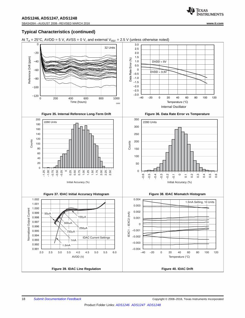
Figure 35. Internal Reference Long-Term Drift
Internal Oscillator
Figure 36. Data Rate Error vs Temperature
Figure 37. IDAC Initial Accuracy Histogram Figure 38. IDAC Mismatch Histogram
Figure 39. IDAC Line Regulation Figure 40. IDAC Drift

800
700
600
500
400
300
200
100
0
Temperature ( C)°
An
alo
g C
urr
en
t (
A)
m
-40 -20 0 20 40 60 80 100 120
5/10/20SPS
40/80/160SPS
320/640/1kSPS
2kSPSAVDD = 5V
330
310
290
270
250
230
210
190
Temperature ( C)°
Dig
ital C
urr
ent (
A)
m
-40 -20 0 20 40 60 80 100 120
5/10/20SPS
40/80/160SPS
320/640/1kSPS
2kSPS
DVDD = 5V
600
550
500
450
400
350
300
250
200
150
100
Data Rate (SPS)
Analo
g C
urr
ent (
A)
m
5 10 20 40 80 160 320 640 1000 2000
AVDD = 5V
AVDD = 3.3V
290
270
250
230
210
190
170
Data Rate (SPS)
Dig
ital C
urr
ent (
A)
m
5 10 20 40 80 160 320 640 1000 2000
DVDD = 3.3V
DVDD = 5V
0
0.1
0.2
0.3
0.4
0.5
0.6
0.7
0.8
0.9
1
1.1
0 1 2 3 4 5Voltage (V)
Nor
mal
ized
IDA
C C
urre
nt
50µA100µA250µA500µA750µA1mA1.5mA
0.98
0.985
0.99
0.995
1
1.005
1.01
0 1 2 3 4 5Voltage (V)
Nor
mal
ized
IDA
C C
urre
nt
19
ADS1246, ADS1247, ADS1248www.ti.com SBAS426H –AUGUST 2008–REVISED MARCH 2016
Product Folder Links: ADS1246 ADS1247 ADS1248
Submit Documentation FeedbackCopyright © 2008–2016, Texas Instruments Incorporated
Typical Characteristics (continued)At TA = 25°C, AVDD = 5 V, AVSS = 0 V, and external VREF = 2.5 V (unless otherwise noted)
Figure 41. IDAC Voltage Compliance Figure 42. IDAC Voltage Compliance
Figure 43. Analog Supply Current vs Data Rate Figure 44. Digital Supply Current vs Data Rate
Figure 45. Analog Supply Current vs Temperature Figure 46. Digital Supply Current vs Temperature

700
600
500
400
300
200
100
0
Temperature ( C)°
An
alo
g C
urr
en
t (
A)
m
-40 -20 0 20 40 60 80 100 120
5/10/20SPS
40/80/160SPS
320/640/1kSPS
2kSPS
AVDD = 3.3V310
290
270
250
230
210
190
Temperature ( C)°
Dig
ita
l C
urr
en
t (
A)
m
-40 -20 0 20 40 60 80 100 120
5/10/20SPS
40/80/160SPS
320/640/1kSPS
2kSPSDVDD = 3.3V
20
ADS1246, ADS1247, ADS1248SBAS426H –AUGUST 2008–REVISED MARCH 2016 www.ti.com
Product Folder Links: ADS1246 ADS1247 ADS1248
Submit Documentation Feedback Copyright © 2008–2016, Texas Instruments Incorporated
Typical Characteristics (continued)At TA = 25°C, AVDD = 5 V, AVSS = 0 V, and external VREF = 2.5 V (unless otherwise noted)
Figure 47. Analog Supply Current vs Temperature Figure 48. Digital Supply Current vs Temperature

21
ADS1246, ADS1247, ADS1248www.ti.com SBAS426H –AUGUST 2008–REVISED MARCH 2016
Product Folder Links: ADS1246 ADS1247 ADS1248
Submit Documentation FeedbackCopyright © 2008–2016, Texas Instruments Incorporated
8 Parameter Measurement Information
8.1 Noise PerformanceThe ADC noise performance is optimized by adjusting the data rate and PGA setting. Generally, the lowest input-referred noise is achieved using the highest gain possible, consistent with the input signal range. Do not set thegain too high or the result is ADC overrange. Noise also depends on the output data rate. As the data ratereduces, the ADC bandwidth correspondingly reduces. This reduction in total bandwidth results in lower overallnoise. Table 1 to Table 6 summarize the noise performance of the device. The data are representative of typicalnoise performance at TA = 25°C. The data shown are the result of averaging the readings from multiple devicesand were measured with the inputs shorted together. A minimum of 128 consecutive readings were used tocalculate the root mean square (RMS) and peak-to-peak (PP) noise for each reading.
Table 1, Table 3, and Table 5 list the input-referred noise in units of μVRMS and μVPP for the conditions shown.Table 2, Table 4, and Table 6 list the corresponding data in units of ENOB (effective number of bits) whereENOB for the RMS noise is defined as in Equation 1:
ENOB = ln((2 · VREF/Gain) / VNRMS) / ln(2)
where VNRMS = Input referred RMS noise voltage (1)
ENOB for the peak-to-peak noise is calculated with the same method.
Table 3 to Table 6 use the internal reference available on the ADS1247 and ADS1248. The data are alsorepresentative of the ADS1246 noise performance when using a low-noise external reference such as theREF5025 or the REF5020.
Table 1. Noise in μVRMS and (μVPP)at AVDD = 5 V, AVSS = 0 V, and External Reference = 2.5 V
DATARATE(SPS)
PGA SETTING
1 2 4 8 16 32 64 128
5 1.1 (4.99) 0.68 (3.8) 0.37 (1.9) 0.19 (0.98) 0.1 (0.44) 0.07 (0.31) 0.05 (0.27) 0.05 (0.21)10 1.53 (8.82) 0.82 (3.71) 0.5 (2.69) 0.27 (1.33) 0.15 (0.67) 0.08 (0.5) 0.06 (0.36) 0.07 (0.34)20 2.32 (13.37) 1.23 (6.69) 0.71 (3.83) 0.34 (1.9) 0.18 (1.01) 0.12 (0.71) 0.10 (0.51) 0.09 (0.54)40 2.72 (17.35) 1.33 (7.65) 0.68 (3.83) 0.38 (2.21) 0.22 (1.13) 0.14 (0.77) 0.15 (0.78) 0.14 (0.76)80 3.56 (22.67) 1.87 (12.3) 0.81 (5.27) 0.5 (3.49) 0.3 (1.99) 0.19 (1.24) 0.19 (1.16) 0.18 (1.04)
160 5.26 (42.03) 2.52 (17.57) 1.32 (9.22) 0.67 (5.25) 0.41 (2.89) 0.26 (1.91) 0.27 (1.74) 0.26 (1.74)320 9.39 (74.91) 4.68 (39.48) 2.69 (18.95) 1.24 (9.94) 0.68 (5.25) 0.45 (3.08) 0.38 (2.71) 0.36 (2.46)640 13.21 (119.66) 6.93 (59.31) 3.59 (28.55) 1.53 (10.68) 0.95 (8.7) 0.63 (4.94) 0.53 (3.74) 0.5 (3.55)1000 32.34 (443.91) 16.11 (185.67) 11.54 (92.23) 4.65 (37.55) 2.02 (23.14) 1.15 (12.29) 0.77 (7.42) 0.64 (4.98)2000 32.29 (372.54) 15.99 (182.27) 8.02 (91.73) 4.08 (45.89) 2.19 (24.14) 1.36 (12.32) 1.08 (8.03) 1.0 (6.93)

22
ADS1246, ADS1247, ADS1248SBAS426H –AUGUST 2008–REVISED MARCH 2016 www.ti.com
Product Folder Links: ADS1246 ADS1247 ADS1248
Submit Documentation Feedback Copyright © 2008–2016, Texas Instruments Incorporated
Table 2. Effective Number of Bits from RMS Noise and (Peak-to-Peak Noise)at AVDD = 5 V, AVSS = 0 V, and External Reference = 2.5 V
DATARATE(SPS)
PGA SETTING
1 2 4 8 16 32 64 128
5 22.1 (19.9) 21.8 (19.3) 21.7 (19.3) 21.6 (19.3) 21.6 (19.4) 21.1 (18.9) 20.6 (18.1) 19.6 (17.5)10 21.6 (19.1) 21.5 (19.4) 21.3 (18.8) 21.1 (18.8) 21 (18.8) 20.9 (18.3) 20.3 (17.7) 19.1 (16.8)20 21 (18.5) 21 (18.5) 20.7 (18.3) 20.8 (18.3) 20.7 (18.2) 20.3 (17.7) 19.6 (17.2) 18.7 (16.1)40 20.8 (18.1) 20.8 (18.3) 20.8 (18.3) 20.6 (18.1) 20.4 (18.1) 20.1 (17.6) 19 (16.6) 18.1 (15.6)80 20.4 (17.8) 20.4 (17.6) 20.6 (17.9) 20.3 (17.5) 20 (17.3) 19.6 (16.9) 18.6 (16) 17.7 (15.2)160 19.9 (16.9) 19.9 (17.1) 19.9 (17) 19.8 (16.9) 19.5 (16.7) 19.2 (16.3) 18.1 (15.5) 17.2 (14.5)320 19 (16) 19 (16) 18.8 (16) 18.9 (15.9) 18.8 (15.9) 18.4 (15.6) 17.6 (14.8) 16.7 (14)640 18.5 (15.4) 18.5 (15.4) 18.4 (15.4) 18.6 (15.8) 18.3 (15.1) 17.9 (14.9) 17.2 (14.4) 16.3 (13.4)
1000 17.2 (13.5) 17.2 (13.7) 16.7 (13.7) 17 (14) 17.2 (13.7) 17.1 (13.6) 16.6 (13.4) 15.9 (12.9)2000 17.2 (13.7) 17.3 (13.7) 17.2 (13.7) 17.2 (13.7) 17.1 (13.7) 16.8 (13.6) 16.1 (13.2) 15.3 (12.5)
Table 3. Noise in μVRMS and (μVPP)at AVDD = 5 V, AVSS = 0 V, and Internal Reference = 2.048 V
DATARATE(SPS)
PGA SETTING
1 2 4 8 16 32 64 128
5 1.35 (7.78) 0.7 (4.17) 0.35 (2.03) 0.17 (0.95) 0.1 (0.53) 0.06 (0.32) 0.05 (0.31) 0.05 (0.29)10 1.8 (10.82) 0.88 (5.26) 0.5 (2.75) 0.24 (1.47) 0.13 (0.8) 0.09 (0.49) 0.07 (0.39) 0.07 (0.4)20 2.62 (14.32) 1.22 (7.05) 0.66 (3.88) 0.35 (2.05) 0.19 (1.09) 0.12 (0.66) 0.1 (0.61) 0.1 (0.55)40 2.64 (16.29) 1.34 (7.75) 0.69 (4.06) 0.35 (2.07) 0.21 (1.15) 0.15 (0.85) 0.14 (0.81) 0.13 (0.75)80 3.69 (23.62) 1.82 (10.81) 0.89 (5.48) 0.51 (2.68) 0.3 (1.69) 0.21 (1.32) 0.2 (1.09) 0.18 (0.98)
160 5.7 (35.74) 2.63 (16.9) 1.34 (8.82) 0.68 (4.24) 0.4 (2.65) 0.3 (1.92) 0.28 (1.88) 0.26 (1.57)320 9.67 (67.44) 4.95 (35.3) 2.59 (17.52) 1.29 (8.86) 0.72 (4.35) 0.49 (3.03) 0.4 (2.44) 0.37 (2.34)640 13.66 (93.06) 7.04 (45.2) 3.63 (18.73) 1.84 (12.97) 1.02 (6.51) 0.68 (4.2) 0.58 (3.69) 0.53 (3.5)1000 31.18 (284.59) 16 (129.77) 7.58 (61.3) 3.98 (33.04) 2.08 (16.82) 1.16 (9.08) 0.83 (5.42) 0.68 (4.65)2000 31.42 (273.39) 15.45 (130.68) 8.07 (67.13) 4.06 (36.16) 2.29 (19.22) 1.38 (9.87) 1.06 (6.93) 1.0 (6.48)
Table 4. Effective Number of Bits from RMS Noise and (Peak-to-Peak Noise)at AVDD = 5 V, AVSS = 0 V, and Internal Reference = 2.048 V
DATARATE(SPS)
PGA SETTING
1 2 4 8 16 32 64 128
5 21.5 (19) 21.5 (18.9) 21.5 (18.9) 21.5 (19) 21.3 (18.9) 21 (18.6) 20.2 (17.7) 19.2 (16.8)10 21.1 (18.5) 21.1 (18.6) 21 (18.4) 21 (18.4) 20.9 (18.3) 20.5 (18) 19.8 (17.3) 18.7 (16.3)20 20.6 (18.1) 20.7 (18.1) 20.6 (18) 20.5 (17.9) 20.4 (17.8) 20.1 (17.6) 19.2 (16.7) 18.3 (15.8)40 20.6 (17.9) 20.5 (18) 20.5 (17.9) 20.5 (17.9) 20.2 (17.8) 19.7 (17.2) 18.8 (16.3) 17.9 (15.4)80 20.1 (17.4) 20.1 (17.5) 20.1 (17.5) 20 (17.5) 19.7 (17.2) 19.2 (16.6) 18.3 (15.8) 17.5 (15)160 19.5 (16.8) 19.6 (16.9) 19.5 (16.8) 19.5 (16.9) 19.3 (16.6) 18.7 (16) 17.8 (15.1) 16.9 (14.3)320 18.7 (15.9) 18.7 (15.8) 18.6 (15.8) 18.6 (15.8) 18.4 (15.8) 18 (15.4) 17.3 (14.7) 16.4 (13.7)640 18.2 (15.4) 18.1 (15.5) 18.1 (15.7) 18.1 (15.3) 17.9 (15.3) 17.5 (14.9) 16.8 (14.1) 15.9 (13.2)
1000 17 (13.8) 17 (13.9) 17 (14) 17 (13.9) 16.9 (13.9) 16.8 (13.8) 16.2 (13.5) 15.5 (12.7)2000 17 (13.9) 17 (13.9) 17 (13.9) 16.9 (13.8) 16.8 (13.7) 16.5 (13.7) 15.9 (13.2) 15 (12.3)

23
ADS1246, ADS1247, ADS1248www.ti.com SBAS426H –AUGUST 2008–REVISED MARCH 2016
Product Folder Links: ADS1246 ADS1247 ADS1248
Submit Documentation FeedbackCopyright © 2008–2016, Texas Instruments Incorporated
Table 5. Noise in μVRMS and (μVPP)at AVDD = 3 V, AVSS = 0 V, and Internal Reference = 2.048 V
DATARATE(SPS)
PGA SETTING
1 2 4 8 16 32 64 128
5 2.5 (14.24) 1.32 (6.92) 0.67 (3.48) 0.32 (1.68) 0.17 (0.9) 0.09 (0.51) 0.08 (0.42) 0.07 (0.39)10 3.09 (16.85) 1.69 (9.32) 0.82 (4.68) 0.42 (2.41) 0.23 (1.18) 0.11 (0.63) 0.11 (0.66) 0.1 (0.55)20 4.55 (24.74) 2.19 (12.82) 1.07 (5.94) 0.55 (3.38) 0.28 (1.66) 0.16 (1.0) 0.15 (0.92) 0.14 (0.87)40 5.06 (34.59) 2.39 (14.49) 1.27 (7.75) 0.66 (4.01) 0.36 (2.18) 0.21 (1.16) 0.21 (1.27) 0.15 (0.84)80 6.63 (43.46) 3.28 (20.22) 1.79 (10.64) 0.89 (5.48) 0.47 (2.95) 0.29 (1.63) 0.28 (1.64) 0.21 (1.24)
160 9.75 (68.28) 4.89 (32.19) 2.36 (17.74) 1.26 (9.87) 0.65 (4.77) 0.4 (2.6) 0.4 (2.7) 0.3 (2.12)320 19.22 (140.06) 9.8 (82.24) 4.81 (32.74) 2.47 (18.59) 1.27 (9.45) 0.71 (5.83) 0.5 (3.36) 0.43 (2.86)640 27.07 (192.96) 13.54 (100.26) 6.88 (49.07) 3.4 (25.93) 1.76 (12.49) 1.02 (7.49) 0.71 (4.81) 0.6 (4.06)1000 40.83 (388.28) 20.39 (185.96) 10.39 (89.38) 5.09 (43.28) 2.66 (22.78) 1.45 (11.01) 0.93 (6.74) 0.74 (4.86)2000 42.06 (322.85) 21.15 (166.75) 10.66 (92.68) 5.61 (44.08) 2.92 (23.06) 1.68 (11.71) 1.19 (8.23) 1.05 (6.97)
Table 6. Effective Number of Bits from RMS and (Peak-to-Peak Noise)at AVDD = 3 V, AVSS = 0 V, and Internal Reference = 2.048 V
DATARATE(SPS)
PGA SETTING
1 2 4 8 16 32 64 128
5 20.6 (18.1) 20.6 (18.2) 20.5 (18.2) 20.6 (18.2) 20.5 (18.1) 20.4 (17.9) 19.6 (17.2) 18.8 (16.3)10 20.3 (17.9) 20.2 (17.7) 20.3 (17.7) 20.2 (17.7) 20.1 (17.7) 20.1 (17.6) 19.1 (16.6) 18.3 (15.8)20 19.8 (17.3) 19.8 (17.3) 19.9 (17.4) 19.8 (17.2) 19.8 (17.2) 19.6 (17) 18.7 (16.1) 17.8 (15.2)40 19.6 (16.9) 19.7 (17.1) 19.6 (17.0) 19.6 (17) 19.5 (16.8) 19.2 (16.8) 18.2 (15.6) 17.7 (15.2)80 19.2 (16.5) 19.3 (16.6) 19.1 (16.6) 19.1 (16.5) 19 (16.4) 18.7 (16.3) 17.8 (15.3) 17.2 (14.7)160 18.7 (15.9) 18.7 (16) 18.7 (15.8) 18.6 (15.7) 18.6 (15.7) 18.3 (15.6) 17.3 (14.5) 16.7 (13.9)320 17.7 (14.8) 17.7 (14.6) 17.7 (14.9) 17.7 (14.7) 17.6 (14.7) 17.5 (14.4) 17 (14.2) 16.2 (13.4)640 17.2 (14.4) 17.2 (14.3) 17.2 (14.3) 17.2 (14.3) 17.1 (14.3) 16.9 (14.1) 16.5 (13.7) 15.7 (12.9)
1000 16.6 (13.4) 16.6 (13.4) 16.6 (13.5) 16.6 (13.5) 16.6 (13.5) 16.4 (13.5) 16.1 (13.2) 15.4 (12.7)2000 16.6 (13.6) 16.6 (13.6) 16.6 (13.4) 16.5 (13.5) 16.4 (13.4) 16.2 (13.4) 15.7 (12.9) 14.9 (12.2)

AIN0/IEXC
AIN1/IEXC
BurnoutDetect
BurnoutDetect
3rd Orderû
Modulator
AVDD REFP1 REFN1 DVDD
ADS1247ADS1248
SCLK
DIN
DRDY
DOUT/DRDY
CS
START
RESET
DGNDCLKAVSS
InputMux
VBIAS
PGAAdjustable
DigitalFilter
SerialInterface
AndControl
Internal Oscillator
AIN2/IEXC/GPIO2
AIN3/IEXC/GPIO3
AIN4/IEXC/GPIO4
AIN5/IEXC/GPIO5
AIN6/IEXC/GPIO6
AIN7/IEXC/GPIO7
REFP0/GPIO0
REFN0/GPIO1
VREF Mux VoltageReference
GPIO
SystemMonitor
VREFOUT VREFCOM
IEXC1 IEXC2
ADS1248 Only
ADS1248 Only
DualIDACs
ADS1248 Only
AINP
AINN
BurnoutDetect
BurnoutDetect
3rd Orderû
Modulator
AVDD REFP REFN DVDD
ADS1246
SCLK
DIN
DRDY
DOUT/DRDY
CS
START
RESET
DGNDCLKAVSS
InputMux
VBIAS
PGAAdjustable
DigitalFilter
SerialInterface
AndControl
Internal Oscillator
24
ADS1246, ADS1247, ADS1248SBAS426H –AUGUST 2008–REVISED MARCH 2016 www.ti.com
Product Folder Links: ADS1246 ADS1247 ADS1248
Submit Documentation Feedback Copyright © 2008–2016, Texas Instruments Incorporated
9 Detailed Description
9.1 OverviewThe ADS1246, ADS1247 and ADS1248 devices are highly integrated 24-bit data converters. The devices includea low-noise, high-input impedance programmable gain amplifier (PGA), a delta-sigma (ΔΣ) ADC with anadjustable single-cycle settling digital filter, internal oscillator, and an SPI-compatible serial interface.
The ADS1247 and ADS1248 also include a flexible input multiplexer with system monitoring capability andgeneral-purpose I/O settings, a very low-drift voltage reference, and two matched current sources for sensorexcitation. Figure 49 and Figure 50 show the various functions incorporated in each device.
9.2 Functional Block Diagram
Figure 49. ADS1246 Block Diagram
Figure 50. ADS1247, ADS1248 Block Diagram

System Monitors
Temperature
DiodeVREFP
VREFN
VREFP1/4
VREFN1/4
VREFP0/4
VREFN0/4
AVDD/4
AVSS/4
DVDD/4
DGND/4ADS1248 Only
ADS1247/48 Only
VBIAS
AIN0
AIN1
VBIAS
AIN2
VBIAS
AIN3
VBIAS
AIN4
VBIAS
AIN5
VBIAS
AIN6
VBIAS
AIN7
AVDD
IDAC1IDAC2
AVDD
VBIAS
PGA
AINP
AVSS
AVDD
Burnout Current Source
(0.5 A, 2 A, 10m m mA)
Burnout Current Source
(0.5 A, 2 A, 10m m mA)
AINN
To
ADC
AVSS
AVSS
AVSS
AVSS
AVSS
AVSS
AVSS
AVSS
AVDD
AVDD
AVDD
AVDD
AVDD
AVDD
AVDD
AVDD
AVDD AVDD
25
ADS1246, ADS1247, ADS1248www.ti.com SBAS426H –AUGUST 2008–REVISED MARCH 2016
Product Folder Links: ADS1246 ADS1247 ADS1248
Submit Documentation FeedbackCopyright © 2008–2016, Texas Instruments Incorporated
9.3 Feature Description
9.3.1 ADC Input and MultiplexerThe ADC measures the input signal through the onboard PGA. All analog inputs are connected to the internalAINP or AINN analog inputs through the analog multiplexer. Figure 51 shows a block diagram of the analog inputmultiplexer.
The input multiplexer connects to eight (ADS1248) or four (ADS1247) analog inputs. Any analog input pin can beselected as the positive input or negative input through the MUX0 register, while the ADS1246 has AINP andAINN connections for a single differential channel. The multiplexer also allows the on-chip excitation current andbias voltage to be selected to a specific channel.
Through the input multiplexer, the ambient temperature (internal temperature sensor), AVDD, DVDD, andexternal reference are all selectable for measurement. See System Monitor for details.
On the ADS1247 and ADS1248, the analog inputs can also be configured as general-purpose inputs and outputs(GPIOs). See General-Purpose Digital I/O for more details.
Figure 51. Analog Input Multiplexer Circuit

454 +
+454
7.5 pF
7.5 pF
7.5 pF
7.5 pF
C
A1
A2
R
RADC
AINP
AINN
RG
RF
RF
¸¹
ᬩ
§ dd¸
¹
ᬩ
§
2GainV
V 0.1 AVDDV2
GainV V 0.1 AVSS MAX IN
CMMAX IN
26
ADS1246, ADS1247, ADS1248SBAS426H –AUGUST 2008–REVISED MARCH 2016 www.ti.com
Product Folder Links: ADS1246 ADS1247 ADS1248
Submit Documentation Feedback Copyright © 2008–2016, Texas Instruments Incorporated
ESD diodes protect the ADC inputs. To prevent these diodes from turning on, make sure the voltages on theanalog input pins do not drop below AVSS by more than 100 mV, and do not exceed AVDD by more than 100mV, as shown in Equation 2. The same caution is true if the inputs are configured to be GPIOs.
AVSS – 100 mV < V(AINX) < AVDD + 100 mV (2)
9.3.2 Low-Noise PGAThe ADS1246, ADS1247, and ADS1248 feature a low-drift, low-noise, high input impedance programmable gainamplifier (PGA). The PGA can be set to gains of 1, 2, 4, 8, 16, 32, 64, or 128 by register SYS0. Figure 52 showsa simplified diagram of the PGA.
The PGA consists of two chopper-stabilized amplifiers (A1 and A2) and a resistor feedback network that sets thegain of the PGA. The PGA input is equipped with an electromagnetic interference (EMI) filter, as shown inFigure 52. Note that as with any PGA, ensure that the input voltage stays within the specified common-modeinput range. The common-mode input voltage (VCM) must be within the range shown in Equation 3.
(3)
Figure 52. Simplified Diagram of the PGA
Gain is changed inside the device using a variable resistor, RG. The differential full-scale input voltage range(FSR) of the PGA is defined by the gain setting and the reference voltage used, as shown in Equation 4.
FSR = ±VREF / Gain (4)
Table 7 shows the corresponding full-scale input ranges when using the internal 2.048-V reference.
Table 7. PGA Full-Scale RangePGA GAIN SETTING FSR
1 ±2.048 V2 ±1.024 V4 ±0.512 V8 ±0.256 V16 ±0.128 V32 ±0.064 V64 ±0.032 V128 ±0.016 V

AINP
RF
A1
AINN
RF
A2
RG
OUTP
OUTN
½ VIN
½ Gain·VIN
+
-
+
-
½ VIN
VCM = ½ (V(AINP) + V(AINN))
½ Gain·VIN
27
ADS1246, ADS1247, ADS1248www.ti.com SBAS426H –AUGUST 2008–REVISED MARCH 2016
Product Folder Links: ADS1246 ADS1247 ADS1248
Submit Documentation FeedbackCopyright © 2008–2016, Texas Instruments Incorporated
9.3.2.1 PGA Common-Mode Voltage RequirementsTo stay within the linear operating range of the PGA, the input signals must meet certain requirements that arediscussed in this section.
The outputs of both amplifiers (A1 and A2) in Figure 52 can not swing closer to the supplies (AVSS and AVDD)than 100 mV. If the outputs OUTP and OUTN are driven to within 100 mV of the supply rails, the amplifierssaturate and consequently become nonlinear. To prevent this nonlinear operating condition, the output voltagesmust meet Equation 5.
AVSS + 0.1 V ≤ V(OUTN), V(OUTP) ≤ AVDD – 0.1 V (5)
Translating the requirements of Equation 5 into requirements referred to the PGA inputs (AINP and AINN) isbeneficial because there is no direct access to the outputs of the PGA. The PGA employs a symmetrical design;therefore, the common-mode voltage at the output of the PGA can be assumed to be the same as the common-mode voltage of the input signal, as shown in Figure 53.
Figure 53. PGA Common-Mode Voltage
The common-mode voltage is calculated using Equation 6.VCM = ½ (V(AINP) + V(AINN)) = ½ (V(OUTP) + V(OUTN)) (6)
The voltages at the PGA inputs (AINP and AINN) can be expressed as Equation 7 and Equation 8.V(AINP) = VCM + ½ VIN (7)V(AINN) = VCM – ½ VIN (8)
The output voltages (V(OUTP) and V(OUTN)) can then be calculated as Equation 9 and Equation 10.V(OUTP) = VCM + ½ Gain · VIN (9)V(OUTN) = VCM – ½ Gain · VIN (10)
The requirements for the output voltages of amplifiers A1 and A2 (Equation 5) can now be translated intorequirements for the input common-mode voltage range using Equation 9 and Equation 10, which are given inEquation 11 and Equation 12.
VCM (MIN) ≥ AVSS + 0.1 V + ½ Gain · VIN (MAX) (11)VCM (MAX) ≤ AVDD – 0.1 V – ½ Gain · VIN (MAX) (12)
To calculate the minimum and maximum common-mode voltage limits, the maximum differential input voltage(VIN (MAX)) that occurs in the application must be used. VIN (MAX) can be less than the maximum possible full-scalevalue.

V(AINP) = 0.95 V
RF
A1
V(AINN) = 0.85 V
RF
A2
RF / 7.5
V(OUTP) = 1.7 V
V(OUTN) = 0.1 V
50 mV
800 mV
+
-
+
-
50 mV
VCM = 0.9 V
800 mV
28
ADS1246, ADS1247, ADS1248SBAS426H –AUGUST 2008–REVISED MARCH 2016 www.ti.com
Product Folder Links: ADS1246 ADS1247 ADS1248
Submit Documentation Feedback Copyright © 2008–2016, Texas Instruments Incorporated
9.3.2.2 PGA Common-Mode Voltage Calculation ExampleThe following paragraphs explain how to apply Equation 11 and Equation 12 to a hypothetical application. Thesetup for this example is AVDD = 3.3 V, AVSS = 0 V, and gain = 16, using an external reference, VREF = 2.5 V.The maximum possible differential input voltage VIN = (V(AINP) – V(AINN)) that can be applied is then limited to thefull-scale range of FSR = ±2.5 V / 16 = ±0.156 V. Consequently, Equation 11 and Equation 12 yield an allowedVCM range of 1.35 V ≤ VCM ≤ 1.95 V.
If the sensor signal connected to the inputs in this hypothetical application does not make use of the entire full-scale range but is limited to VIN (MAX) = ±0.1 V, for example, then this reduced input signal amplitude relaxes theVCM restriction to 0.9 V ≤ VCM ≤ 2.4 V.
In the case of a fully-differential sensor signal, each input (AINP, AINN) can swing up to ±50 mV around thecommon-mode voltage (V(AINP) + V(AINN)) / 2, which must remain between the limits of 0.9 V and 2.4 V. Theoutput of a symmetrical wheatstone bridge is an example of a fully-differential signal. Figure 54 shows a situationwhere the common-mode voltage of the input signal is at the lowest limit. V(OUTN) is exactly at 0.1 V in this case.Any further decrease in common-mode voltage (VCM) or increase in differential input voltage (VIN) drives V(OUTN)below 0.1 V and saturates amplifier A2.
Figure 54. Example where VCM is at Lowest Limit
In contrast, the signal of an RTD is of a pseudo-differential nature (if implemented as shown in one of theapplication example sections, 3-Wire RTD Measurement), where the negative input is held at a constant voltageother than 0 V and only the voltage on the positive input changes. When a pseudo-differential signal must bemeasured, the negative input in this example must be biased at a voltage from 0.85 V to 2.35 V. The positiveinput can then swing up to VIN (MAX) = 100 mV above the negative input. In this case, the common-mode voltagechanges at the same time the voltage on the positive input changes. That is, while the input signal swingsbetween 0 V ≤ VIN ≤ VIN (MAX), the common-mode voltage swings between V(AINN) ≤ VCM ≤ V(AINN) + ½ VIN (MAX).Satisfying the common-mode voltage requirements for the maximum input voltage VIN (MAX) ensures therequirements are met throughout the entire signal range.
Figure 55 and Figure 56 show examples of both fully-differential and pseudo-differential signals, respectively.

0 V
1.0 V
AINP
AINN
100 mVVCM
0 V
1.0 V
AINP
AINN
100 mVVCM
29
ADS1246, ADS1247, ADS1248www.ti.com SBAS426H –AUGUST 2008–REVISED MARCH 2016
Product Folder Links: ADS1246 ADS1247 ADS1248
Submit Documentation FeedbackCopyright © 2008–2016, Texas Instruments Incorporated
(1) Input current with VCM = 2.5 V. TA = 25°C, AVDD = 5 V, and AVSS = 0 V.
Figure 55. Fully-Differential Input Signal Figure 56. Pseudo-Differential Input Signal
NOTEWith a unipolar power supply, the input range does not extend to the ground. Equation 11and Equation 12 show the common-mode voltage requirements.• VCM (MIN) ≥ AVSS + 0.1 V + ½ Gain · VIN (MAX)• VCM (MAX) ≤ AVDD – 0.1 V – ½ Gain · VIN (MAX)
9.3.2.3 Analog Input ImpedanceThe device inputs are buffered through a high-input impedance PGA before they reach the ΔΣ modulator. For themajority of applications, the input current is minimal and can be neglected. However, because the PGA ischopper-stabilized for noise and offset performance, the input impedance is best described as a small absoluteinput current. The absolute input current for selected channels is approximately proportional to the selectedmodulator clock. Table 8 shows the typical values for these currents with a differential voltage coefficient and thecorresponding input impedances over data rate.
Table 8. Typical Values for Analog Input Current over Data Rate (1)
CONDITION ABSOLUTE INPUT CURRENT EFFECTIVE INPUT IMPEDANCEDR = 5 SPS, 10 SPS, 20 SPS ± (0.5 nA + 0.1 nA/V) 5000 MΩ
DR = 40 SPS, 80 SPS, 160 SPS ± (2 nA + 0.5 nA/V) 1200 MΩDR = 320 SPS, 640 SPS, 1 kSPS ± (4 nA + 1 nA/V) 600 MΩ
DR = 2 kSPS ± (8 nA + 2 nA/V) 300 MΩ
9.3.3 Clock SourceThe device can use either the internal oscillator or an external clock. Connect the CLK pin to DGND beforepower up or reset to activate the internal oscillator. Connecting an external clock to the CLK pin at any timedeactivates the internal oscillator, with the device then operating on the external clock. After the device switchesto the external clock, it cannot be switched back to the internal oscillator without cycling the power supplies orresetting the device.

30
ADS1246, ADS1247, ADS1248SBAS426H –AUGUST 2008–REVISED MARCH 2016 www.ti.com
Product Folder Links: ADS1246 ADS1247 ADS1248
Submit Documentation Feedback Copyright © 2008–2016, Texas Instruments Incorporated
9.3.4 ModulatorA third-order delta-sigma modulator is used in the ADS1246, ADS1247, and ADS1248 devices. The modulatorconverts the analog input voltage into a pulse code modulated (PCM) data stream. To save power, the modulatorclock runs from 32 kHz up to 512 kHz for different data rates, as shown in Table 9.
(1) Using the internal oscillator or an external 4.096-MHz clock.
Table 9. Modulator Clock Frequency for Different Data RatesDATA RATE
(SPS)MODULATOR RATE (fMOD) (1)
(kHz) fCLK/fMOD
5, 10, 20 32 12840, 80, 160 128 32
320, 640, 1000 256 162000 512 8
(1) Values shown for fCLK = 4.096 MHz.
9.3.5 Digital FilterThe ADC uses linear-phase finite impulse response (FIR) digital filters that can be adjusted for different outputdata rates. The digital filter always settles in a single cycle.
Table 10 shows the exact data rates when an external clock equal to 4.096 MHz is used. Also shown is thesignal –3-dB bandwidth, and the 50-Hz and 60-Hz attenuation. For good 50-Hz or 60-Hz rejection, use a datarate of 20 SPS or slower.
The frequency responses of the digital filter are shown in Figure 57 to Figure 67. Figure 60 illustrates a detailedview of the filter frequency response from 48 Hz to 62 Hz for a 20-SPS data rate. All filter plots are generatedwith a 4.096-MHz external clock.
Data rates and digital filter frequency responses scale proportionally with changes in the system clock frequency.The internal oscillator frequency has a variation, as specified in Electrical Characteristics that will also affect datarates and the digital filter frequency response.
Table 10. Digital Filter Specifications (1)
NOMINALDATA RATE
ACTUALDATA RATE
–3-dBBANDWIDTH
ATTENUATIONfIN = 50 Hz ±0.3 Hz fIN = 60 Hz ±0.3 Hz fIN = 50 Hz ±1 Hz fIN = 60 Hz ±1 Hz
5 SPS 5.018 SPS 2.26 Hz –106 dB –74 dB –81 dB –69 dB10 SPS 10.037 SPS 4.76 Hz –106 dB –74 dB –80 dB –69 dB20 SPS 20.075 SPS 14.8 Hz –71 dB –74 dB –66 dB –68 dB40 SPS 40.15 SPS 9.03 Hz — — — —80 SPS 80.301 SPS 19.8 Hz — — — —160 SPS 160.6 SPS 118 Hz — — — —320 SPS 321.608 SPS 154 Hz — — — —640 SPS 643.21 SPS 495 Hz — — — —1000 SPS 1000 SPS 732 Hz — — — —2000 SPS 2000 SPS 1465 Hz — — — —

200
0
-20
-40
-60
-80
-100
-120
0 400 600
Frequency (Hz)
Ma
gn
itu
de
(d
B)
800 1000 1200 1400 1600 1800 2000 200
0
-20
-40
-60
-80
-100
-120
0 400 600
Frequency (Hz)
Ga
in (
dB
)
800 1000 1200 1400 1600 1800 2000
20
0
-20
-40
-60
-80
-100
-120
0 40 60
Frequency (Hz)
Magnitude (
dB
)
80 100 120 140 160 180 200 50 52 54 56 58 60
-60
-70
-80
-90
-100
-110
-120
48
Frequency (Hz)
Magnitude (
dB
)
62
20
0
-20
-40
-60
-80
-100
-120
0 40 60
Frequency (Hz)
Magnitude (
dB
)
80 100 120 140 160 180 200 20
0
-20
-40
-60
-80
-100
-120
0 40 60
Frequency (Hz)
Magnitude (
dB
)
80 100 120 140 160 180 200
31
ADS1246, ADS1247, ADS1248www.ti.com SBAS426H –AUGUST 2008–REVISED MARCH 2016
Product Folder Links: ADS1246 ADS1247 ADS1248
Submit Documentation FeedbackCopyright © 2008–2016, Texas Instruments Incorporated
space
Figure 57. Filter Profile with Data Rate = 5 SPS Figure 58. Filter Profile with Data Rate = 10 SPS
Figure 59. Filter Profile with Data Rate = 20 SPS Figure 60. Detailed View of Filter Profile with Data Rate =20 SPS Between 48 Hz and 62 Hz
Figure 61. Filter Profile with Data Rate = 40 SPS Figure 62. Filter Profile with Data Rate = 80 SPS

2
0
-20
-40
-60
-80
-100
-120
0 4 6
Frequency (kHz)
Magnitude (
dB
)
8 10 12 14 16 18 20
500
0
-20
-40
-60
-80
-100
-120
0 1000 1500
Frequency (Hz)
Ma
gn
itu
de
(d
B)
2000 2500 3000 3500 4000 4500 5000 1
0
-20
-40
-60
-80
-100
-120
0 2 3
Frequency (kHz)
Magnitude (
dB
)
4 5 6 7 8 9 10
200
0
-20
-40
-60
-80
-100
-120
0 400 600
Frequency (Hz)
Ma
gn
itu
de
(d
B)
800 1000 1200 1400 1600 1800 2000 500
0
-20
-40
-60
-80
-100
-120
0 1000 1500
Frequency (Hz)
Ma
gn
itu
de
(d
B)
2000 2500 3000 3500 4000 4500 5000
32
ADS1246, ADS1247, ADS1248SBAS426H –AUGUST 2008–REVISED MARCH 2016 www.ti.com
Product Folder Links: ADS1246 ADS1247 ADS1248
Submit Documentation Feedback Copyright © 2008–2016, Texas Instruments Incorporated
Figure 63. Filter Profile with Data Rate = 160 SPS Figure 64. Filter Profile with Data Rate = 320 SPS
Figure 65. Filter Profile with Data Rate = 640 SPS Figure 66. Filter Profile with Data Rate = 1 kSPS
Figure 67. Filter Profile with Data Rate = 2 kSPS

REFN1REFP1
ADC
ADS1248 Only
REFN0REFP0
REFNREFP
VREFCOMVREFOUT
Reference Multiplexer
Internal
Voltage
Reference
33
ADS1246, ADS1247, ADS1248www.ti.com SBAS426H –AUGUST 2008–REVISED MARCH 2016
Product Folder Links: ADS1246 ADS1247 ADS1248
Submit Documentation FeedbackCopyright © 2008–2016, Texas Instruments Incorporated
9.3.6 Voltage Reference InputThe voltage reference for the device is the differential voltage between REFP and REFN, given by Equation 13:
VREF = V(REFP) – V(REFN) (13)
In the case of the ADS1246, these pins are dedicated inputs. For the ADS1247 and ADS1248, there is amultiplexer that selects the reference inputs, as shown in Figure 68. The reference input uses a buffer toincrease the input impedance.
As with the analog inputs, REFP0 and REFN0 can be configured as digital I/Os on the ADS1247 and ADS1248.
Figure 68. Reference Input Multiplexer
The reference input circuit has ESD diodes to protect the inputs. To prevent the diodes from turning on, makesure the voltage on the reference input pin is not less than AVSS – 100 mV, and does not exceed AVDD + 100mV, as shown in Equation 14.
AVSS – 100 mV < (V(REFP) or V(REFN)) < AVDD + 100 mV (14)
9.3.7 Internal Voltage ReferenceThe ADS1247 and ADS1248 have an internal voltage reference with a low temperature coefficient. The output ofthe voltage reference is 2.048 V (nominal) with the capability of both sourcing and sinking up to 10 mA of current.
The voltage reference must have a capacitor connected between VREFOUT and VREFCOM. The value of thecapacitance must be in the range of 1 μF to 47 μF. Large values provide more noise filtering of the reference;however, the turnon time increases with capacitance, as shown in Table 11. For stability reasons, VREFCOMmust have a path with an impedance less than 10 Ω to AC ground nodes, such as GND (for a 0-V to 5-V analogpower supply), or AVSS (for a ±2.5-V analog power supply). In case this impedance is higher than 10 Ω, connecta capacitor of at least 0.1 μF between VREFCOM and an AC ground node (for example, GND).
NOTEBecause time is required for the voltage reference to settle to the final voltage, take carewhen the device is turned off between conversions. Allow adequate time for the internalreference to fully settle before starting a new conversion.
Table 11. Internal Reference Settling TimeVREFOUT CAPACITOR SETTLING ERROR TIME TO REACH THE SETTLING ERROR
1 μF±0.5% 70 μs±0.1% 110 μs
4.7 μF±0.5% 290 μs±0.1% 375 μs
47 μF±0.5% 2.2 ms±0.1% 2.4 ms

34
ADS1246, ADS1247, ADS1248SBAS426H –AUGUST 2008–REVISED MARCH 2016 www.ti.com
Product Folder Links: ADS1246 ADS1247 ADS1248
Submit Documentation Feedback Copyright © 2008–2016, Texas Instruments Incorporated
The internal reference is controlled by the MUX1 register; by default, the internal reference is off after power up(see ADS1247 and ADS1248 Detailed Register Definitions for more details). Therefore, the internal referencemust first be turned on and then connected through the internal reference multiplexer. Because the internalreference is used to generate the current reference for the excitation current sources, it must be turned on beforethe excitation currents become available.
9.3.8 Excitation Current SourcesThe ADS1247 and ADS1248 provide two matched excitation current sources (IDACs) for RTD applications. Forthree-wire RTD applications, the matched current sources can be used to cancel the errors caused by sensorlead resistance. The output current of the IDACs can be programmed to 50 μA, 100 μA, 250 μA,500 μA, 750 μA, 1000 μA, or 1500 μA.
The two matched current sources can be connected to dedicated current output pins IEXC1 and IEXC2(ADS1248 only), or to any analog input pin (ADS1247 and ADS1248); see ADS1247 and ADS1248 DetailedRegister Definitions for more information. Both current sources can be connected to the same pin. The internalreference must be turned on and the proper amount of capacitance applied to VREFOUT when using theexcitation current sources.
9.3.9 Sensor DetectionTo help detect a possible sensor malfunction, the device provides selectable current sources (0.5 μA, 2 μA, or10 μA) to act as burn-out current sources. When enabled, one current source sources current to the selectedpositive analog input (AINP) while the other current source sinks current from the selected negative analog input(AINN).
In case of an open circuit in the sensor, these burn-out current sources pull the positive input towards AVDD andthe negative input towards AVSS, resulting in a full-scale reading. A full-scale reading may also indicate that thesensor is overloaded or that the reference voltage is absent. A near-zero reading may indicate a shorted sensor.The absolute value of the burn-out current sources typically varies by ±10% and the internal multiplexer adds asmall series resistance. Therefore, distinguishing a shorted sensor condition from a normal reading can bedifficult, especially if an RC filter is used at the inputs. In other words, even if the sensor is shorted, the voltagedrop across the external filter resistance and the residual resistance of the multiplexer causes the output to reada value higher than zero.
The ADC readings of a functional sensor may be corrupted when the burn-out current sources are enabled. TIrecommends disabling the burn-out current sources when performing the precision measurement, and onlyenabling them to test for sensor fault conditions.
9.3.10 Bias Voltage GenerationA selectable bias voltage is provided for use with unbiased thermocouples. The bias voltage is (AVDD + AVSS) /2 and can be applied to any analog input channel through the internal input multiplexer. The bias voltage turnontimes for different sensor capacitances are listed in Table 12.
The internal bias voltage generator, when selected on multiple channels, causes them to be internally shorted.Because of this, take care to limit the amount of current that may flow through the device. TI recommends thatunder no circumstances should more than 5 mA be allowed to flow through this path. This applies when thedevice is in operation and when it is powered down.
Table 12. Bias Voltage Settling TimeSENSOR CAPACITANCE SETTLING TIME
0.1 μF 220 μs1 μF 2.2 ms10 μF 22 ms
200 μF 450 ms

IOCFG
AINx/GPIOx
To Analog Mux
DIO WRITE
IODIR
DIO READ
REFx0/GPIOx
35
ADS1246, ADS1247, ADS1248www.ti.com SBAS426H –AUGUST 2008–REVISED MARCH 2016
Product Folder Links: ADS1246 ADS1247 ADS1248
Submit Documentation FeedbackCopyright © 2008–2016, Texas Instruments Incorporated
9.3.11 General-Purpose Digital I/OThe ADS1248 has eight pins and the ADS1247 has four pins that serve a dual purpose as either analog inputsor general-purpose digital inputs and outputs (GPIOs).
Three registers control the function of the GPIO pins. Use the GPIO configuration register (IOCFG) to enable apin as a GPIO pin. The GPIO direction register (IODIR) configures the GPIO pin as either an input or an output.Finally, the GPIO data register (IODAT) contains the GPIO data. If a GPIO pin is configured as an input, therespective IODAT[x] bit reads the status of the pin; if a GPIO pin is configured as an output, write the outputstatus to the respective IODAT[x] bit. For more information about the use of GPIO pins, please see the ADS1247and ADS1248 Detailed Register Definitions section.
Figure 69 shows a diagram of how these functions are combined onto a single pin. Note that when the pin isconfigured as a GPIO, the corresponding logic is powered from AVDD and AVSS. When the ADS1247 andADS1248 are operated with bipolar analog supplies, the GPIO outputs bipolar voltages. Care must be takenloading the GPIO pins when used as outputs because large currents can cause droop or noise on the analogsupplies.
Figure 69. Analog and Data Interface Pin
9.3.12 System MonitorThe ADS1247 and ADS1248 provide a system monitor function. This function can measure the analog powersupply, digital power supply, external voltage reference, or ambient temperature. Note that the system monitorfunction provides a coarse result. When the system monitor is enabled, the analog inputs are disconnected.
9.3.12.1 Power-Supply MonitorThe system monitor can measure the analog or digital power supply. When measuring the power supply (VSP),the resulting conversion is approximately 1/4 of the actual power supply voltage, as shown in Equation 15.
Conversion Result = (VSP / 4) / VREF (15)
9.3.12.2 External Voltage Reference MonitorThe ADC can measure the external voltage reference. In this configuration, the monitored external voltagereference (VREX) is connected to the analog input. The result (conversion code) is approximately 1/4 of the actualreference voltage, as shown in Equation 16.
Conversion Result = (VREX / 4) / VREF (16)
NOTEThe internal reference voltage must be enabled when measuring an external voltagereference using the system monitor.
9.3.12.3 Ambient Temperature MonitorOn-chip diodes provide temperature-sensing capability. When selecting the temperature monitor function, theanodes of two diodes are connected to the ADC. Typically, the difference in diode voltage is 118 mV atTA = 25°C with a temperature coefficient of 405 μV/°C.

START
SCLK
1 24
DRDY
ADS1246/47/48Status
Converting Power Down
DOUT/DRDY
2 3
tSTART
tCONV
36
ADS1246, ADS1247, ADS1248SBAS426H –AUGUST 2008–REVISED MARCH 2016 www.ti.com
Product Folder Links: ADS1246 ADS1247 ADS1248
Submit Documentation Feedback Copyright © 2008–2016, Texas Instruments Incorporated
9.4 Device Functional Modes
9.4.1 Power UpWhen DVDD is powered up, the internal power-on reset module generates a pulse that resets all digital circuitry.All the digital circuits are held in a reset state for 216 system clocks to allow the analog circuits and the internaldigital power supply to settle. SPI communication cannot occur until the internal reset is released.
9.4.2 ResetWhen the RESET pin goes low, the device is immediately reset. All registers are restored to default values. Thedevice stays in reset mode as long as the RESET pin stays low. When the RESET pin goes high, the ADCcomes out of reset mode and is able to convert data. After the RESET pin goes high, and when the system clockfrequency is 4.096 MHz, the digital filter and the registers are held in a reset state for 0.6 ms whenfCLK = 4.096 MHz. Therefore, valid SPI communication can only be resumed 0.6 ms after the RESET pin goeshigh; see Figure 4. When the RESET pin goes low, the clock selection is reset to the internal oscillator.
A reset can also be performed by the RESET command through the serial interface and is functionally the sameas using the RESET pin. For information about using the RESET command, see RESET (0000 011X).
9.4.3 Power-Down ModePower consumption is reduced to a minimum by placing the device into power-down mode. There are two waysto put the device into power-down mode: using the SLEEP command and taking the START pin low.
During power-down mode, the internal reference status depends on the setting of the VREFCON bits in theMUX1 register; see Register Maps for details.
9.4.4 Conversion ControlThe START pin provides precise control of conversions. Pulse the START pin high to begin a conversion, asshown in Figure 70 and Table 13. The conversion completion is indicated by the DRDY pin going low and withthe DOUT/DRDY pin when the DRDY MODE bit is 1 in the IDAC0 register. When the conversion completes, thedevice automatically powers down. During power down, the conversion result can be retrieved; however, STARTmust be taken high before communicating with the configuration registers. The device stays powered down untilthe START pin is returned high to begin a new conversion. When the START pin is returned high, the decimationfilter is held in a reset state for 32 modulator clock cycles internally to allow the analog circuits to settle.
Holding the START pin high will configure the device to continuously convert as shown in Figure 71.
Figure 70. Timing for Single Conversion Using the Start Pin

Converting Converting Converting Converting
START
DOUT/DRDY
ADS1246/47/48
Status
Data Ready Data Ready Data Ready
37
ADS1246, ADS1247, ADS1248www.ti.com SBAS426H –AUGUST 2008–REVISED MARCH 2016
Product Folder Links: ADS1246 ADS1247 ADS1248
Submit Documentation FeedbackCopyright © 2008–2016, Texas Instruments Incorporated
(1) For fCLK = 4.096MHz
Table 13. Start Pin Conversion Times for Figure 70 (1)
SYMBOL DESCRIPTION DATA RATE (SPS) VALUE UNIT
tCONVTime from the START rising edge to DRDY and
DOUT/DRDY going low
5 200.295 ms
10 100.644 ms
20 50.825 ms
40 25.169 ms
80 12.716 ms
160 6.489 ms
320 3.247 ms
640 1.692 ms
1000 1.138 ms
2000 0.575 ms
NOTE: SCLK held low in this example.
Figure 71. Timing for Conversion With Start Pin High
With the START pin held high, the ADC converts the selected input channels continuously. This configurationcontinues until the START pin is taken low. The START pin can also be used to perform synchronizedmeasurements for multi-channel applications by pulsing the START pin. With multiple devices, if each devicereceives the START pin pulse at the same time, all devices start a conversion on the rise of the start pin. If alldevices are operating with the same data rate, all of the devices complete the conversion at the same time.
Conversions can also be initiated through SPI commands as well. Similar to using the START pin, the device canbe put into a power-down mode using the SLEEP command. Functionally, this is similar to taking the START pinlow. To initiate a conversion, the WAKEUP command powers up the ADC and starts a conversion, similar toreturning the START pin high. Note that the START pin must be held high to use commands to controlconversions. Do not combine using the START pin and using commands to control conversions.
Also, sending a SYNC command immediately starts a new ADC conversion. For the SYNC command, the digitalfilter is reset, starting a new conversion without completing the previous conversion. This is useful insynchronizing conversions from multiple devices or maintaining periodic timing from multiple channels.
Similarly, writing to any of the first four registers (MUX0, VBIAS, MUX1, or SYS0; addresses 00h to 04h)automatically resets the digital filter. A change in any of these registers makes the appropriate setup change inthe device, but also restarts the conversion similar to a SYNC command.
9.4.4.1 Settling Time for Channel MultiplexingThe device is a true single-cycle settling ΔΣ converter. The first data available after the start of a conversion arefully settled and valid for use, provided that the input signal has settled to its final result. The time required tosettle is roughly equal to the inverse of the data rate. The exact time depends on the specific data rate and theoperation that resulted in the start of a conversion; see Table 14 for specific values.

38
ADS1246, ADS1247, ADS1248SBAS426H –AUGUST 2008–REVISED MARCH 2016 www.ti.com
Product Folder Links: ADS1246 ADS1247 ADS1248
Submit Documentation Feedback Copyright © 2008–2016, Texas Instruments Incorporated
9.4.4.2 Channel Cycling and Overload RecoveryWhen cycling through channels, take care when configuring the device to ensure that settling occurs within onecycle. For setups that cycle through MUX channels, but do not change PGA and data rate settings, changing theMUX0 register is sufficient. However, when changing PGA and data rate settings, ensure that an overloadedcondition cannot occur during the transmission. When configuration register data are transferred to the device,new settings become active at the end of each register byte sent. Therefore, a brief overload condition can occurduring the transmission of configuration data after the completion of the MUX0 byte and before completion of theSYS0 byte. This temporary overload can result in intermittent incorrect readings. To ensure that an overloaddoes not occur, it may be necessary to split the communication into two separate communications allowing thechange of the SYS0 register before the change of the MUX0 register.
In the event of an overloaded state, take care to ensure single-cycle settling into the next cycle. Because thedevice implements a chopper-stabilized PGA, changing data rates during an overload state can cause thechopper to become unstable. This instability results in slow settling time. To prevent this slow settling, alwayschange the PGA setting or MUX setting to a non-overloaded state before changing the data rate.
9.4.4.3 Single-Cycle SettlingThe ADS1246, ADS1247, and ADS1248 are capable of single-cycle settling across all gains and data rates.However, to achieve single-cycle settling at 2 kSPS, special care must be taken with respect to the interfaceusing WREG to change a configuration register. When operating at 2 kSPS, the SCLK period must not exceed520 ns, and the time between the beginning of writing a register byte data and the beginning of a subsequentregister byte data must not exceed 4.2 µs. Additionally, when performing multiple individual write commands tothe first four registers, wait at least 64 system clocks before initiating another write command.
9.4.4.4 Digital Filter Reset OperationApart from the RESET command and the RESET pin, the digital filter is reset automatically when either a writeoperation to the MUX0, VBIAS, MUX1, or SYS0 registers is performed, when a SYNC command is issued, or theSTART pin is taken high.
The filter is reset four system clocks (tCLK) after the falling edge of the seventh SCLK of the SYNC command.Similarly, if any write operation takes place in the MUX0 register, regardless of whether the register valuechanged or not, the filter is reset after the completion of the MUX0 write.
If any write activity takes place in the VBIAS, MUX1, or SYS0 registers, regardless of whether the register valuechanged or not, the filter is reset. The reset pulse lasts for 32 modulator clocks after the completion of the writeoperation. If there are multiple write operations, the resulting reset pulse may be viewed as the ANDed result ofthe different active low pulses created individually by each action.
Table 14 shows the conversion time after a filter reset. Note that this time depends on the operation initiating thereset. Also, the first conversion after a filter reset has a slightly different time than the second and subsequentconversions.

calingS OffsetV 1.251calingS Gain
V 2!
Final Output Data = (Input OFC[2:0])- ´
FSC[2:0]
400000h
ADC S
OFC
Register
Final
Output
Output Data
Clipped to 24 Bits´
+
-
FSC Register
400000h
39
ADS1246, ADS1247, ADS1248www.ti.com SBAS426H –AUGUST 2008–REVISED MARCH 2016
Product Folder Links: ADS1246 ADS1247 ADS1248
Submit Documentation FeedbackCopyright © 2008–2016, Texas Instruments Incorporated
(1) For fCLK = 4.096 MHz.
Table 14. Data Conversion Time
NOMINALDATA RATE
(SPS)
EXACT DATARATE(SPS)
FIRST DATA CONVERSION TIME AFTER FILTER RESET
SECOND AND SUBSEQUENTCONVERSION TIME AFTER
FILTER RESETSYNC COMMAND, MUX0
REGISTER WRITE
HARDWARE RESET, RESETCOMMAND, START PIN HIGH,WAKEUP COMMAND, VBIAS,
MUX1, or SYS0 REGISTERWRITE
(ms) (1)NO. OF
SYSTEMCLOCKCYCLES
(ms) (1)NO. OF
SYSTEMCLOCKCYCLES
(ms) (1)NO. OF
SYSTEMCLOCKCYCLES
5 5.019 199.258 816160 200.26 820265 199.250 81612810 10.038 99.633 408096 100.635 412201 99.625 40806420 20.075 49.820 204064 50.822 208169 49.812 20403240 40.151 24.92 102072 25.172 103106 24.906 10201680 80.301 12.467 51064 12.719 52098 12.453 51008160 160.602 6.240 25560 6.492 26594 6.226 25504320 321.608 3.124 12796 3.25 13314 3.109 12736640 643.216 1.569 6428 1.695 6946 1.554 63681000 1000 1.014 4156 1.141 4674 1 40962000 2000 0.514 2108 0.578 2370 0.5 2048
9.4.5 CalibrationThe conversion data are scaled by offset and gain registers before yielding the final output code. As shown inFigure 72, the output of the digital filter is first subtracted by the offset register (OFC) and then multiplied by thefull-scale register (FSC) to digitally scale the gain. A digital clipping circuit ensures that the output code does notexceed 24 bits. Equation 17 shows the scaling.
Figure 72. Calibration Block Diagram
(17)
The values of the offset and full-scale registers are set by writing to them directly, or they are set automaticallyby calibration commands.
The offset and gain calibration features are intended for correction of minor system level offset and gain errors.When entering manual values into the calibration registers, care must be taken to avoid scaling down the gainregister to values far below a scaling factor of 1.0. Under extreme situations it is possible to over-range the ADC.Avoid encountering situations where analog inputs are connected to voltages greater than VREF / gain.
Take care when increasing digital gain with the FSC. When implementing custom digital gains less than 20%higher than nominal and offsets less than 40% of full scale, no special care is required. When operating at digitalgains greater than 20% higher than nominal and offsets greater than 40% of full scale, make sure that the offsetand gain registers follow the conditions of Equation 18.
(18)
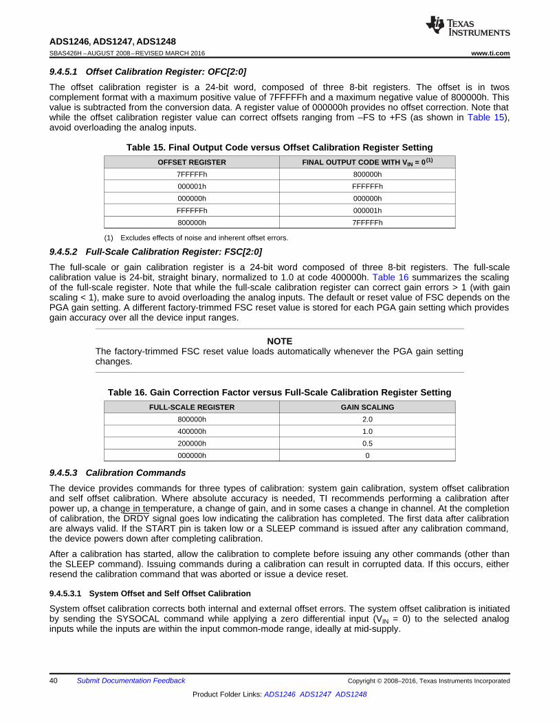
40
ADS1246, ADS1247, ADS1248SBAS426H –AUGUST 2008–REVISED MARCH 2016 www.ti.com
Product Folder Links: ADS1246 ADS1247 ADS1248
Submit Documentation Feedback Copyright © 2008–2016, Texas Instruments Incorporated
9.4.5.1 Offset Calibration Register: OFC[2:0]The offset calibration register is a 24-bit word, composed of three 8-bit registers. The offset is in twoscomplement format with a maximum positive value of 7FFFFFh and a maximum negative value of 800000h. Thisvalue is subtracted from the conversion data. A register value of 000000h provides no offset correction. Note thatwhile the offset calibration register value can correct offsets ranging from –FS to +FS (as shown in Table 15),avoid overloading the analog inputs.
(1) Excludes effects of noise and inherent offset errors.
Table 15. Final Output Code versus Offset Calibration Register SettingOFFSET REGISTER FINAL OUTPUT CODE WITH VIN = 0 (1)
7FFFFFh 800000h000001h FFFFFFh000000h 000000hFFFFFFh 000001h800000h 7FFFFFh
9.4.5.2 Full-Scale Calibration Register: FSC[2:0]The full-scale or gain calibration register is a 24-bit word composed of three 8-bit registers. The full-scalecalibration value is 24-bit, straight binary, normalized to 1.0 at code 400000h. Table 16 summarizes the scalingof the full-scale register. Note that while the full-scale calibration register can correct gain errors > 1 (with gainscaling < 1), make sure to avoid overloading the analog inputs. The default or reset value of FSC depends on thePGA gain setting. A different factory-trimmed FSC reset value is stored for each PGA gain setting which providesgain accuracy over all the device input ranges.
NOTEThe factory-trimmed FSC reset value loads automatically whenever the PGA gain settingchanges.
Table 16. Gain Correction Factor versus Full-Scale Calibration Register SettingFULL-SCALE REGISTER GAIN SCALING
800000h 2.0400000h 1.0200000h 0.5000000h 0
9.4.5.3 Calibration CommandsThe device provides commands for three types of calibration: system gain calibration, system offset calibrationand self offset calibration. Where absolute accuracy is needed, TI recommends performing a calibration afterpower up, a change in temperature, a change of gain, and in some cases a change in channel. At the completionof calibration, the DRDY signal goes low indicating the calibration has completed. The first data after calibrationare always valid. If the START pin is taken low or a SLEEP command is issued after any calibration command,the device powers down after completing calibration.
After a calibration has started, allow the calibration to complete before issuing any other commands (other thanthe SLEEP command). Issuing commands during a calibration can result in corrupted data. If this occurs, eitherresend the calibration command that was aborted or issue a device reset.
9.4.5.3.1 System Offset and Self Offset Calibration
System offset calibration corrects both internal and external offset errors. The system offset calibration is initiatedby sending the SYSOCAL command while applying a zero differential input (VIN = 0) to the selected analoginputs while the inputs are within the input common-mode range, ideally at mid-supply.

DATAMODCLKCAL f
16f32
f50
tTimenCalibratio
41
ADS1246, ADS1247, ADS1248www.ti.com SBAS426H –AUGUST 2008–REVISED MARCH 2016
Product Folder Links: ADS1246 ADS1247 ADS1248
Submit Documentation FeedbackCopyright © 2008–2016, Texas Instruments Incorporated
The self offset calibration is initiated by sending the SELFOCAL command. During self offset calibration, theselected inputs are disconnected from the internal circuitry and a zero differential signal is applied internally,connecting the inputs to mid-supply. With both offset calibrations the offset calibration register (OFC) is updatedafterwards. When either offset calibration command is issued, the device stops the current conversion and startsthe calibration procedure immediately. An offset calibration should be performed before a gain calibration.
9.4.5.3.2 System Gain Calibration
System gain calibration corrects for gain error in the signal path. The system gain calibration is initiated bysending the SYSGCAL command while applying a full-scale input to the selected analog inputs. Afterwards thefull-scale calibration register (FSC) is updated. When a system gain calibration command is issued, the devicestops the current conversion and starts the calibration procedure immediately.
9.4.5.4 Calibration TimingWhen calibration is initiated, the device performs 16 consecutive data conversions and averages the results tocalculate the calibration value. This provides a more accurate calibration value. The time required for calibrationis shown in Table 17 and can be calculated using Equation 19:
where fDATA is the data rate. (19)
(1) For fCLK = 4.096 MHz.
Table 17. Calibration Time Versus Data RateDATA RATE
(SPS)CALIBRATION TIME (tCAL)
(ms) (1)
5 3201.0110 1601.0120 801.01240 400.2680 200.26160 100.14320 50.14640 25.141000 16.142000 8.07
9.5 Programming
9.5.1 Serial InterfaceThe device provides an SPI-compatible serial communication interface plus a data ready signal (DRDY).Communication is full-duplex with the exception of a few limitations in regards to the RREG command and theRDATA command. These limitations are explained in detail in Commands. For the basic serial interface timingcharacteristics, see Figure 1 and Figure 2 of this document.
9.5.1.1 Chip Select (CS)The CS pin activates SPI communication. CS must be low before data transactions and must stay low for theentire SPI communication period. When CS is high, the DOUT/DRDY pin enters a high-impedance state.Therefore, reading and writing to the serial interface are ignored and the serial interface is reset. DRDY pinoperation is independent of CS. DRDY will still indicate that a new conversion has completed and is forced highas a response to SCLK, even if CS is high.
Taking CS high deactivates only the SPI communication with the device. Data conversion continues and theDRDY signal can be monitored to check if a new conversion result is ready. A master device monitoring theDRDY signal can select the appropriate slave device by pulling the CS pin low.

SCLK
D[23]
1 2 22 1 2 823 243
D[22] D[21] D[2] D[1] D[0]DOUT/ (1)DRDY
DRDY
42
ADS1246, ADS1247, ADS1248SBAS426H –AUGUST 2008–REVISED MARCH 2016 www.ti.com
Product Folder Links: ADS1246 ADS1247 ADS1248
Submit Documentation Feedback Copyright © 2008–2016, Texas Instruments Incorporated
Programming (continued)9.5.1.2 Serial Clock (SCLK)SCLK provides the clock for serial communication. SCLK is a Schmitt-trigger input, but TI recommends keepingSCLK as free from noise as possible to prevent glitches from inadvertently shifting the data. Data are shifted intoDIN on the falling edge of SCLK and shifted out of DOUT on the rising edge of SCLK.
9.5.1.3 Data Input (DIN)DIN is used along with SCLK to send data to the device. Data on DIN are shifted into the device on the fallingedge of SCLK.
The communication of this device is full-duplex in nature. The device monitors commands shifted in even whendata are being shifted out. Data that are present in the output shift register are shifted out when sending in acommand. Therefore, make sure that whatever is being sent on the DIN pin is valid when shifting out data. Whenno command is to be sent to the device when reading out data, send the NOP command on DIN.
9.5.1.4 Data Ready (DRDY)The DRDY pin goes low to indicate a new conversion is complete, and the conversion result is stored in theconversion result buffer. SCLK must be held low for tDTS after the DRDY low transition (see Figure 2) so that theconversion result is loaded into both the result buffer and the output shift register. Therefore, issue no commandsduring this time frame if the conversion result is to be read out later. This constraint applies only when CS isasserted and the device is in RDATAC mode. When CS is not asserted, SPI communication with other deviceson the SPI bus does not affect loading of the conversion result. After the DRDY pin goes low, it is forced high onthe first falling edge of SCLK (so that the DRDY pin can be polled for 0 instead of waiting for a falling edge). Ifthe DRDY pin is not taken high by clocking in SCLKs after it falls low, a short high pulse for a duration of tPWHindicates new data are ready.
9.5.1.5 Data Output and Data Ready (DOUT/DRDY)The DOUT/DRDY pin has two modes: data out (DOUT) only, or DOUT combined with data ready (DRDY). TheDRDY MODE bit determines the function of this pin and can be found in the ID register in the ADS1246 and theIDAC0 register in the ADS1247 and ADS1248. In either mode, the DOUT/DRDY pin goes to a high-impedancestate when CS is taken high.
When the DRDY MODE bit is set to 0, this pin functions as DOUT only. Data are clocked out on the rising edgeof SCLK, MSB first (as shown in Figure 73).
When the DRDY MODE bit is set to 1, this pin functions as both DOUT and DRDY. Data are shifted out as withDOUT, but the pin adds the DRDY function. Note that this mode will not be operational when the device is instop read data continuous mode when the SDATAC command is given.
The DRDY MODE bit modifies only the DOUT/DRDY pin functionality. The DRDY pin functionality remainsunaffected.
(1) CS tied low.
Figure 73. Data Retrieval with the DRDY MODE Bit = 0 (Disabled)
When the DRDY MODE bit is enabled and a new conversion is complete, DOUT/DRDY goes low if it is high. If itis already low, then DOUT/DRDY goes high and then goes low (as shown in Figure 74). Similar to the DRDY pin,a falling edge on the DOUT/DRDY pin signals that a new conversion result is ready. After DOUT/DRDY goeslow, the data can be clocked out by providing 24 SCLKs if the device is in read data continuous mode. In order toforce DOUT/DRDY high (so that DOUT/DRDY can be polled for a 0 instead of waiting for a falling edge), a no

SCLK
DOUT/DRDY(1)
DIN
1 2 8
RREG
1 2 8
00h
1 2 8
NOP
1 2 8
NOP
XXh
SCLK
DOUT/DRDY(1)
DIN
DRDY
1 2 242322
D[21]
3
D[23] D[22] D[2] D[0]D[1]
1 2 24
D[23] D[22] D[0]
1 2 8
NOPNOP NOP
SCLK
DOUT/DRDY(1)
DIN
DRDY
1 2 242322
D[21]
3
D[23] D[22] D[2] D[0]D[1]
1 2 24
D[23] D[22] D[0]
NOP NOPNOP
43
ADS1246, ADS1247, ADS1248www.ti.com SBAS426H –AUGUST 2008–REVISED MARCH 2016
Product Folder Links: ADS1246 ADS1247 ADS1248
Submit Documentation FeedbackCopyright © 2008–2016, Texas Instruments Incorporated
Programming (continued)operation command (NOP) or any other command that does not load the data output register can be sent afterreading out the data. Because SCLKs can only be sent in multiples of eight, a NOP can be sent to forceDOUT/DRDY high if no other command is pending. The DOUT/DRDY pin goes high after the first rising edge ofSCLK after reading the conversion result completely (as shown in Figure 75). The same condition also appliesafter an RREG command. After all the register bits have been read out, the first rising edge of SCLK forcesDOUT/DRDY high. Figure 76 shows an example where sending an extra NOP command after reading out aregister with an RREG command forces the DOUT/DRDY pin high.
(1) CS tied low.
Figure 74. Data Retrieval with the DRDY MODE Bit = 1 (Enabled)
(1) DRDY MODE bit enabled, CS tied low.
Figure 75. DOUT/DRDY Forced High after Retrieving the Conversion Result
(1) DRDY MODE bit enabled, CS tied low.
Figure 76. DOUT/DRDY Forced High after Reading Register Data
9.5.1.6 SPI ResetSPI communication is reset in several ways. To reset the serial interface (without resetting the registers or thedigital filter), the CS pin can be pulled high. Taking the RESET pin low resets the serial interface along with allthe other digital functions. It will also return all registers to their default values and start a new conversion.
In systems where CS is tied low permanently, register writes must always be fully completed in 8-bit increments.If a glitch on SCLK disrupts SPI communications, commands will not be recognized by the device. The deviceimplements a timeout function for all listed commands in the event that data are corrupted and the CS pin ispermanently tied low. The SPI timeout will reset the interface if idle for 64 conversion cycles.
7FFFFFh
Outp
ut C
ode
-FS ¼ 0 ¼ FS
Input Voltage VIN
7FFFFEh
000001h
¼
000000h
800000h
FFFFFFh
800001h
¼
-FS2 - 1
23
223
FS2 - 1
23
223
44
ADS1246, ADS1247, ADS1248SBAS426H –AUGUST 2008–REVISED MARCH 2016 www.ti.com
Product Folder Links: ADS1246 ADS1247 ADS1248
Submit Documentation Feedback Copyright © 2008–2016, Texas Instruments Incorporated
Programming (continued)9.5.1.7 SPI Communication During Power-Down ModeWhen the START pin is low or the device is in power-down mode, only the RDATA, RDATAC, SDATAC,WAKEUP, and NOP commands can be issued. The RDATA command can be used to repeatedly read the lastconversion result during power-down mode. Other commands do not function because the internal clock is shutdown to save power during power-down mode.
9.5.2 Data FormatThe device provides 24 bits of data in binary twos complement format. The size of one code (LSB) is calculatedusing Equation 20.
1 LSB = (2 × VREF / Gain) / 224 = +FS / 223 (20)
A positive full-scale (FS) input [VIN ≥ (+FS – 1 LSB) = (VREF / Gain – 1 LSB)] produces an output code of7FFFFFh and a negative full-scale input (VIN ≤ –FS = –VREF / Gain) produces an output code of 800000h. Theoutput clips at these codes for signals that exceed full-scale. Table 18 summarizes the ideal output codes fordifferent input signals.
(1) Excludes effects of noise, linearity, offset, and gain errors.
Table 18. Ideal Output Code vs Input SignalINPUT SIGNAL, VIN
(AINP – AINN) IDEAL OUTPUT CODE (1)
≥ FS (223 – 1) / 223 7FFFFFhFS / 223 000001h
0 000000h–FS / 223 FFFFFFh≤ –FS 800000h
Mapping of the analog input signal to the output codes is shown in Figure 77.
Figure 77. Code Transition Diagram
9.5.3 CommandsThe device offers 13 commands to control device operation as shown in Table 19. Some of the commands arestand-alone commands (WAKEUP, SLEEP, SYNC, RESET, SYSOCAL, SYSGCAL, and SELFOCAL). There arethree additional commands used to control the read of data from the device (RDATA, RDATAC, and SDATAC).The commands to read (RREG) and write (WREG) configuration register data from and to the device requireadditional information as part of the instruction. A no-operation command (NOP) can be used to clock out datafrom the device without clocking in a command.
Operands:

45
ADS1246, ADS1247, ADS1248www.ti.com SBAS426H –AUGUST 2008–REVISED MARCH 2016
Product Folder Links: ADS1246 ADS1247 ADS1248
Submit Documentation FeedbackCopyright © 2008–2016, Texas Instruments Incorporated
(1) When the START pin is low or the device is in power-down mode, only the RDATA, RDATAC, SDATAC, WAKEUP, and NOPcommands can be issued.
• n = number of registers to be read or written (number of bytes – 1)• r = register (0 to 15)• x = don't care
Table 19. SPI CommandsCOMMAND (1) DESCRIPTION 1st COMMAND BYTE 2nd COMMAND BYTE
WAKEUP Exit power-down mode 0000 000x (00h, 01h)SLEEP Enter power-down mode 0000 001x (02h, 03h)SYNC Synchronize ADC conversions 0000 010x (04h, 05h) 0000 010x (04,05h)RESET Reset to default values 0000 011x (06h, 07h)
NOP No operation 1111 1111 (FFh)RDATA Read data once 0001 001x (12h, 13h)
RDATAC Read data continuous mode 0001 010x (14h, 15h)SDATAC Stop read data continuous mode 0001 011x (16h, 17h)
RREG Read from register rrrr 0010 rrrr (2xh) 0000 nnnnWREG Write to register rrrr 0100 rrrr (4xh) 0000 nnnn
SYSOCAL System offset calibration 0110 0000 (60h)SYSGCAL System gain calibration 0110 0001 (61h)SELFOCAL Self offset calibration 0110 0010 (62h)
Restricted Restricted command.Never send to the device. 1111 0001 (F1h)
9.5.3.1 WAKEUP (0000 000x)Use the WAKEUP command to power up the device after a SLEEP command. After execution of the WAKEUPcommand, the device powers up on the falling edge of the eighth SCLK.
9.5.3.2 SLEEP (0000 001x)The SLEEP command places the device into power-down mode. When the SLEEP command is issued, thedevice completes the current conversion and then goes into power-down mode. Note that this command doesnot automatically power down the internal voltage reference; see the VREFCON bits in MUX1 for each device forfurther details.
To exit power-down mode, issue the WAKEUP command. Single conversions can be performed by issuing aWAKEUP command followed by a SLEEP command.
Both WAKEUP and SLEEP are the software command equivalents of using the START pin to control the device,as shown in Figure 78.
NOTEIf the START pin is held low, a WAKEUP command will not power up the device. Whenusing the SLEEP command, CS must be held low for the duration of the power-downmode.

DIN
SCLK
0.6 ms
RESET ANY SPI COMMAND
1 8 1 87
4 tCLK
DIN
SCLK
4 tCLK
0000 010X
1 8
0000 010X
SYNC
Synchronization Occurs Here
7
DIN
SCLK
SLEEP
1 8
0000 001X 0000 000X
WAKEUP
CS
DRDY
Status Normal Mode Power-down Mode Normal Mode
Start New ConversionFinish Current Conversion
46
ADS1246, ADS1247, ADS1248SBAS426H –AUGUST 2008–REVISED MARCH 2016 www.ti.com
Product Folder Links: ADS1246 ADS1247 ADS1248
Submit Documentation Feedback Copyright © 2008–2016, Texas Instruments Incorporated
Figure 78. SLEEP and WAKEUP Commands Operation
9.5.3.3 SYNC (0000 010x)The SYNC command resets the ADC digital filter and starts a new conversion. The DRDY pin from multipledevices connected to the same SPI bus can be synchronized by issuing a SYNC command to all of devicessimultaneously.
Figure 79. SYNC Command Operation
9.5.3.4 RESET (0000 011X)The RESET command restores the registers to the respective default values. This command also resets thedigital filter. RESET is the command equivalent of using the RESET pin to reset the device. However, theRESET command does not reset the serial interface. If the RESET command is issued when the serial interfaceis out of synchonization due to a glitch on SCLK, the device does not reset. The CS pin can be used to reset theserial interface first, and then a RESET command can be issued to reset the device. The RESET commandholds the registers and the decimation filter in a reset state for 0.6 ms when the system clock frequency is 4.096MHz, similar to the hardware reset. Therefore, SPI communication can be only be started 0.6 ms after theRESET command is issued, as shown in Figure 80.
Figure 80. SPI Communication after an SPI Reset
9.5.3.5 RDATA (0001 001x)The RDATA command loads the most recent conversion result into the output register. After issuing thiscommand, the conversion result is read out by sending 24 SCLKs, as shown in Figure 81. This command alsoworks in RDATAC mode.

DIN
DOUT
DRDY
RDATAC
SCLK
24 Bits
1 8 1 24
NOP0001 010X
SCLK
DOUT
DIN
DRDY
NOPNOP NOP RDATA NOP NOP
1
D[23] D[14] D[1] D[1] D[0]D[17] D[16] D[15]D[22] D[23] D[22]
2 1 29 107 8 23 24 23 24
D[0]
SCLK
DIN
DOUT
DRDY
MSB
0001 001X
Mid-Byte LSB
1 8 1 24
NOP NOP NOP
RDATA
47
ADS1246, ADS1247, ADS1248www.ti.com SBAS426H –AUGUST 2008–REVISED MARCH 2016
Product Folder Links: ADS1246 ADS1247 ADS1248
Submit Documentation FeedbackCopyright © 2008–2016, Texas Instruments Incorporated
Figure 81. Read Data Once
When performing multiple reads of the conversion result, the RDATA command can be sent when the last eightbits of the conversion result are being shifted out during the course of the first read operation by takingadvantage of the duplex communication nature of the serial interface, as shown in Figure 82.
Figure 82. Using RDATA in Full-Duplex Mode
9.5.3.6 RDATAC (0001 010x)The RDATAC command enables read data continuous mode. This is the default mode after a power up or reset.In read data continuous mode, new conversion results are automatically loaded onto DOUT. The conversionresult can be received from the device after the DRDY signal goes low by sending 24 SCLKs. It is not necessaryto read back all the bits, as long as the number of bits read out is a multiple of eight. The RDATAC commandmust be issued after DRDY goes low, and the command takes effect on the next DRDY.
Be sure to complete data retrieval (conversion result or register read-back) before DRDY returns low, or theresulting data will be corrupt. Successful register read operations in RDATAC mode require the knowledge ofwhen the next DRDY falling edge occurs.
Figure 83. Read Data Continuously
9.5.3.7 SDATAC (0001 011x)The SDATAC command terminates read data continuous mode. In stop read data continuous mode, theconversion result is not automatically loaded onto DOUT when DRDY goes low, and register read operations canbe performed without interruption from new conversion results being loaded into the output shift register. Use theRDATA command to retrieve conversion data. The SDATAC command takes effect after the next DRDY.

DIN 0100 0010 0000 0001 MUX1 SYS0
1st
Command2nd
CommandDataByte
DataByte
DIN
DOUT VBIAS
0010 0001 0000 0001
1st
Command
Byte
2nd
Command
Byte
MUX1
Data Byte Data Byte
48
ADS1246, ADS1247, ADS1248SBAS426H –AUGUST 2008–REVISED MARCH 2016 www.ti.com
Product Folder Links: ADS1246 ADS1247 ADS1248
Submit Documentation Feedback Copyright © 2008–2016, Texas Instruments Incorporated
If DRDY is not actively monitored for data conversions, the stop read data continuous mode is the preferredmethod of reading data. In this mode, a read of ADC data is not interrupted by the completion of a new ADCconversion.
9.5.3.8 RREG (0010 rrrr, 0000 nnnn)The RREG command outputs the data from up to 15 registers, starting with the register address specified as partof the instruction. The number of registers read is one plus the value of the second byte. If the count exceeds theremaining registers, the addresses wrap back to the beginning. The two byte command structure for RREG islisted below.• First Command Byte: 0010 rrrr, where rrrr is the address of the first register to read.• Second Command Byte: 0000 nnnn, where nnnn is the number of bytes to read –1.• Byte(s): data read from the registers are clocked out with NOPs.
It is not possible to use the full-duplex nature of the serial interface when reading out the register data. Forexample, a SYNC command cannot be issued when reading out the VBIAS and MUX1 data, as shown inFigure 84. Any command sent during the readout of the register data is ignored. Thus, TI recommends sendingNOPs through DIN when reading out the register data.
Figure 84. Read from Register
9.5.3.9 WREG (0100 rrrr, 0000 nnnn)The WREG command writes to the registers, starting with the register specified as part of the instruction. Thenumber of registers that are written is one plus the value of the second byte. The command structure for WREGis listed below.• First Command Byte: 0100 rrrr, where rrrr is the address of the first register to be written.• Second Command Byte: 0000 nnnn, where nnnn is the number of bytes to be written – 1.• Byte(s): data to be written to the registers.
Figure 85. Write to Register
9.5.3.10 SYSOCAL (0110 0000)The SYSOCAL command initiates a system offset calibration. For a system offset calibration, the inputs must beexternally shorted to a voltage within the input common mode range. The inputs should be near the mid-supplyvoltage of (AVDD + AVSS) / 2. The OFC register is updated when the command completes. Timing for thecalibration commands can be found in Figure 86.
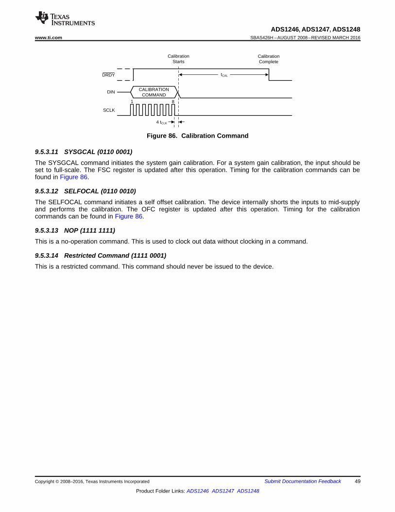
DIN
SCLK
CALIBRATION COMMAND
1 8
DRDY tCAL
Calibration Starts
Calibration Complete
4 tCLK
49
ADS1246, ADS1247, ADS1248www.ti.com SBAS426H –AUGUST 2008–REVISED MARCH 2016
Product Folder Links: ADS1246 ADS1247 ADS1248
Submit Documentation FeedbackCopyright © 2008–2016, Texas Instruments Incorporated
Figure 86. Calibration Command
9.5.3.11 SYSGCAL (0110 0001)The SYSGCAL command initiates the system gain calibration. For a system gain calibration, the input should beset to full-scale. The FSC register is updated after this operation. Timing for the calibration commands can befound in Figure 86.
9.5.3.12 SELFOCAL (0110 0010)The SELFOCAL command initiates a self offset calibration. The device internally shorts the inputs to mid-supplyand performs the calibration. The OFC register is updated after this operation. Timing for the calibrationcommands can be found in Figure 86.
9.5.3.13 NOP (1111 1111)This is a no-operation command. This is used to clock out data without clocking in a command.
9.5.3.14 Restricted Command (1111 0001)This is a restricted command. This command should never be issued to the device.

50
ADS1246, ADS1247, ADS1248SBAS426H –AUGUST 2008–REVISED MARCH 2016 www.ti.com
Product Folder Links: ADS1246 ADS1247 ADS1248
Submit Documentation Feedback Copyright © 2008–2016, Texas Instruments Incorporated
9.6 Register Maps
9.6.1 ADS1246 Register Map
Table 20. ADS1246 Register MapADDRESS REGISTER BIT 7 BIT 6 BIT 5 BIT 4 BIT 3 BIT 2 BIT 1 BIT 0
00h BCS BCS[1:0] 0 0 0 0 0 101h VBIAS 0 0 0 0 0 0 VBIAS[1:0]02h MUX1 CLKSTAT 0 0 0 0 MUXCAL[2:0]03h SYS0 0 PGA[2:0] DR[3:0]04h OFC0 OFC[7:0]05h OFC1 OFC[15:8]06h OFC2 OFC[23:16]07h FSC0 FSC[7:0]08h FSC1 FSC[15:8]09h FSC2 FSC[23:16]
0Ah ID ID[3:0] DRDYMODE 0 0 0
9.6.2 ADS1246 Detailed Register Definitions
9.6.2.1 BCS—Burn-out Current Source Register (offset = 00h) [reset = 01h]These bits control the sensor burn-out detect current source.
Figure 87. Burn-out Current Source Register
7 6 5 4 3 2 1 0BCS[1:0] 0 0 0 0 0 1R/W-0h R-0h R-0h R-0h R-0h R-0h R-1h
LEGEND: R/W = Read/Write; R = Read only; -n = value after reset; -x = variable
Table 21. Burn-out Current Source Register Field DescriptionsBit Field Type Reset Description7:6 BCS[1:0] R/W 0h Burn-out Detect Current Source
These bits control the setting of the sensor burn-out detectcurrent source00: Burn-out current source off (default)01: Burn-out current source on, 0.5 μA10: Burn-out current source on, 2 μA11: Burn-out current source on, 10 μA
5:0 RESERVED R 01h ReservedAlways write 000001

51
ADS1246, ADS1247, ADS1248www.ti.com SBAS426H –AUGUST 2008–REVISED MARCH 2016
Product Folder Links: ADS1246 ADS1247 ADS1248
Submit Documentation FeedbackCopyright © 2008–2016, Texas Instruments Incorporated
9.6.2.2 VBIAS—Bias Voltage Register (offset = 01h) [reset = 00h]This register enables a bias voltage on the analog inputs.
Figure 88. Bias Voltage Register
7 6 5 4 3 2 1 00 0 0 0 0 0 VBIAS[1:0]
R-0h R-0h R-0h R-0h R-0h R-0h R/W-0hLEGEND: R/W = Read/Write; R = Read only; -n = value after reset; -x = variable
Table 22. Bias Voltage Register Field DescriptionsBit Field Type Reset Description7:2 RESERVED R 00h Reserved
Always write 0000001 VBIAS[1] R/W 0h VBIAS[1] Voltage Enable
A bias voltage of mid-supply (AVDD + AVSS) / 2 is applied toAINN0: Bias voltage is not enabled (default)1: Bias voltage is applied to AINN
0 VBIAS[0] R/W 0h VBIAS[0] Voltage EnableA bias voltage of mid-supply (AVDD + AVSS) / 2 is applied toAINP0: Bias voltage is not enabled (default)1: Bias voltage is applied to AINP

52
ADS1246, ADS1247, ADS1248SBAS426H –AUGUST 2008–REVISED MARCH 2016 www.ti.com
Product Folder Links: ADS1246 ADS1247 ADS1248
Submit Documentation Feedback Copyright © 2008–2016, Texas Instruments Incorporated
9.6.2.3 MUX—Multiplexer Control Register (offset = 02h) [reset = x0h]
Figure 89. Multiplexer Control Register
7 6 5 4 3 2 1 0CLKSTAT 0 0 0 0 MUXCAL[2:0]
R-xh R-0h R-0h R-0h R-0h R/W-0hLEGEND: R/W = Read/Write; R = Read only; -n = value after reset; -x = variable
Table 23. Multiplexer Control Register Field DescriptionsBit Field Type Reset Description7 CLKSTAT R xh Clock status
This bit is read-only and indicates whether the internal oscillatoror external clock is being used.0: Internal oscillator in use1: External clock in use
6:3 RESERVED R 0h ReservedAlways write 0000
2:0 MUXCAL R/W 0h System Monitor ControlThese bits are used to select a system monitor. The MUXCALselection supercedes the selections from the VBIAS register.000: Normal operation (default)001: Offset calibration. The analog inputs are disconnected andAINP and AINN are internally connected to mid-supply (AVDD +AVSS) / 2.010: Gain calibration. The analog inputs are connected to thevoltage reference.011: Temperature measurement. The inputs are connected to adiode circuit that produces a voltage proportional to the ambienttemperature of the device.
Table 24 lists the ADC input connection and PGA settings for each MUXCAL setting. The PGA setting reverts tothe original SYS0 register setting when MUXCAL is taken back to normal operation or offset measurement.
Table 24. MUXCAL SettingsMUXCAL[2:0] PGA GAIN SETTING ADC INPUT
000 Set by SYS0 register Normal operation001 Set by SYS0 register Offset calibration: inputs shorted to mid-supply (AVDD + AVSS) / 2010 Forced to 1 Gain calibration: V(REFP) – V(REFN) (full-scale)011 Forced to 1 Temperature measurement diode

53
ADS1246, ADS1247, ADS1248www.ti.com SBAS426H –AUGUST 2008–REVISED MARCH 2016
Product Folder Links: ADS1246 ADS1247 ADS1248
Submit Documentation FeedbackCopyright © 2008–2016, Texas Instruments Incorporated
9.6.2.4 SYS0—System Control Register 0 (offset = 03h) [reset = 00h]
Figure 90. System Control Register 0
7 6 5 4 3 2 1 00 PGA[2:0] DR[3:0]
R-0h R/W-0h R/W-0hLEGEND: R/W = Read/Write; R = Read only; -n = value after reset; -x = variable
Table 25. System Control Register 0 Field DescriptionsBit Field Type Reset Description7 RESERVED R 0h Reserved
This bit must always be set to 06:4 PGA[2:0] R/W 0h Gain Setting for PGA
These bits determine the gain of the PGA000: PGA = 1 (default)001: PGA = 2010: PGA = 4011: PGA = 8100: PGA = 16101: PGA = 32110: PGA = 64111: PGA = 128
3:0 DR[3:0] R/W 0h Data Output Rate SettingThese bits determine the data output rate of the ADC0000: DR = 5 SPS (default)0001: DR = 10 SPS0010: DR = 20 SPS0011: DR = 40 SPS0100: DR = 80 SPS0101: DR = 160 SPS0110: DR = 320 SPS0111: DR = 640 SPS1000: DR = 1000 SPS1001 to 1111: DR = 2000 SPS

54
ADS1246, ADS1247, ADS1248SBAS426H –AUGUST 2008–REVISED MARCH 2016 www.ti.com
Product Folder Links: ADS1246 ADS1247 ADS1248
Submit Documentation Feedback Copyright © 2008–2016, Texas Instruments Incorporated
9.6.2.5 OFC—Offset Calibration Coefficient Registers (offset = 04h, 05h, 06h) [reset = 00h, 00h, 00h]These bits make up the offset calibration coefficient register of the ADS1246.
Figure 91. Offset Calibration Coefficient Registers
7 6 5 4 3 2 1 0OFC[7:0]R/W-00h
15 14 13 12 11 10 9 8OFC[15:8]R/W-00h
23 22 21 20 19 18 17 16OFC[23:16]
R/W-00h
LEGEND: R/W = Read/Write; R = Read only; -n = value after reset; -x = variable
Table 26. Offset Calibration Coefficient Register Field DescriptionsBit Field Type Reset Description
23:0 OFC[23:0] R/W 000000h Offset Calibration RegisterThree registers compose the ADC 24-bit offset calibration word.The 24-bit word is twos complement format and is internally left-shifted to align with the ADC 24-bit conversion result. The ADCsubtracts the register value from the conversion result before fullscale operation.
9.6.2.6 FSC—Full-Scale Calibration Coefficient Registers (offset = 07h, 08h, 09h) [reset = PGAdependent]
These bits make up the full-scale calibration coefficient register. The reset value for FSC is factory-trimmed foreach PGA setting. The factory-trimmed FSC reset value is automatically loaded whenever the PGA setting ischanged.
Figure 92. Full-Scale Calibration Coefficient Registers
7 6 5 4 3 2 4 0FSC[7:0]R/W-xxh
15 14 13 12 11 10 9 8FSC[15:8]R/W-xxh
23 22 21 20 19 18 17 16FSC[23:16]
R/W-xxh
LEGEND: R/W = Read/Write; R = Read only; -n = value after reset; -x = variable
Table 27. Full-Scale Calibration Coefficient Register Field DescriptionsBit Field Type Reset Description
23:0 FSC[23:0] R/W xxxxxxh Full-Scale Calibration RegisterThree registers compose the ADC 24-bit full-scale calibrationword. The 24-bit word is straight binary. The ADC divides theregister value by the FSC register by 400000h to derive thescale factor for calibration. After the offset calibration, the ADCmultiplies the scale factor by the conversion result. The factory-trimmed FSC reset value is automatically loaded whenever thePGA setting is changed.

55
ADS1246, ADS1247, ADS1248www.ti.com SBAS426H –AUGUST 2008–REVISED MARCH 2016
Product Folder Links: ADS1246 ADS1247 ADS1248
Submit Documentation FeedbackCopyright © 2008–2016, Texas Instruments Incorporated
9.6.2.7 ID—ID Register (offset = 0Ah) [reset = x0h]
Figure 93. ID Register
7 6 5 4 3 2 1 0ID[3:0] DRDY MODE 0 0 0R-xh R/W-0h R-0h R-0h R-0h
LEGEND: R/W = Read/Write; R = Read only; -n = value after reset; -x = variable
(1) Cannot be used in SDATAC mode
Table 28. ID Register Field DescriptionsBit Field Type Reset Description7:4 ID[3:0] R xh Revision Identification
Read-only, factory-programmed bits; used for revisionidentification.
3 DRDY MODE R/W 0h Data Ready Mode SettingThis bit sets the DOUT/DRDY pin functionality. In either settingof the DRDY MODE bit, the dedicated DRDY pin continues toindicate data ready, active low.0: DOUT/DRDY pin functions only as Data Out (default)1: DOUT/DRDY pin functions both as Data Out and Data Ready,active low (1)
2:0 RESERVED R 0h RESERVEDThese bits must always be set to 000
9.6.3 ADS1247 and ADS1248 Register Map
Table 29. ADS1247 and ADS1248 Register MapADDRESS REGISTER BIT 7 BIT 6 BIT 5 BIT 4 BIT 3 BIT 2 BIT 1 BIT 0
00h MUX0 BCS[1:0] MUX_SP[2:0] MUX_SN[2:0]01h VBIAS VBIAS[7:0]02h MUX1 CLKSTAT VREFCON[1:0] REFSELT[1:0] MUXCAL[2:0]03h SYS0 0 PGA[2:0] DR[3:0]04h OFC0 OFC[7:0]05h OFC1 OFC[15:8]06h OFC2 OFC[23:16]07h FSC0 FSC[7:0]08h FSC1 FSC[15:8]09h FSC2 FSC[23:16]
0Ah IDAC0 ID[3:0] DRDYMODE IMAG[2:0]
0Bh IDAC1 I1DIR[3:0] I2DIR[3:0]0Ch GPIOCFG IOCFG[7:0]0Dh GPIODIR IODIR[7:0]0Eh GPIODAT IODAT[7:0]

56
ADS1246, ADS1247, ADS1248SBAS426H –AUGUST 2008–REVISED MARCH 2016 www.ti.com
Product Folder Links: ADS1246 ADS1247 ADS1248
Submit Documentation Feedback Copyright © 2008–2016, Texas Instruments Incorporated
9.6.4 ADS1247 and ADS1248 Detailed Register Definitions
9.6.4.1 MUX0—Multiplexer Control Register 0 (offset = 00h) [reset = 01h]This register allows any combination of differential inputs to be selected on any of the input channels. Note thatthis setting can be superceded by the MUXCAL and VBIAS bits.
Figure 94. Multiplexer Control Register 0
7 6 5 4 3 2 1 0BCS[1:0] MUX_SP[2:0] MUX_SN[2:0]R/W-0h R/W-0h R/W-1h
LEGEND: R/W = Read/Write; R = Read only; -n = value after reset; -x = variable
Table 30. Multiplexer Control Register 0 Register Field DescriptionsBit Field Type Reset Description7:6 BCS[1:0] R/W 0h Burn-out Detect Current Source Register
These bits control the setting of the sensor burnout detectcurrent source00: Burn-out current source off (default)01: Burn-out current source on, 0.5 μA10: Burn-out current source on, 2 μA11: Burn-out current source on, 10 μA
5:3 MUX_SP[2:0] R/W 0h Multiplexer Selection - ADC Positive InputPositive input channel selection bits000: AIN0 (default)001: AIN1010: AIN2011: AIN3100: AIN4 (ADS1248 only)101: AIN5 (ADS1248 only)110: AIN6 (ADS1248 only)111: AIN7 (ADS1248 only)
2:0 MUX_SN[2:0] R/W 1h Multiplexer Selection - ADC Negative InputNegative input channel selection bits000: AIN0001: AIN1 (default)010: AIN2011: AIN3100: AIN4 (ADS1248 only)101: AIN5 (ADS1248 only)110: AIN6 (ADS1248 only)111: AIN7 (ADS1248 only)

57
ADS1246, ADS1247, ADS1248www.ti.com SBAS426H –AUGUST 2008–REVISED MARCH 2016
Product Folder Links: ADS1246 ADS1247 ADS1248
Submit Documentation FeedbackCopyright © 2008–2016, Texas Instruments Incorporated
9.6.4.2 VBIAS—Bias Voltage Register (offset = 01h) [reset = 00h]
Figure 95. Bias Voltage Register (ADS1247)
7 6 5 4 3 2 1 00 0 0 0 VBIAS[3:0]
R-0h R-0h R-0h R-0h R/W-0hLEGEND: R/W = Read/Write; R = Read only; -n = value after reset; -x = variable
Table 31. Bias Voltage Register Field Descriptions (ADS1247)Bit Field Type Reset Description7:4 RESERVED R 0h Reserved
Always write 00003 VBIAS[3] R/W 0h VBIAS[3] Voltage Enable
A bias voltage of mid-supply (AVDD + AVSS) / 2 is applied toAIN30: Bias voltage is not enabled (default)1: Bias voltage is applied to AIN3
2 VBIAS[2] R/W 0h VBIAS[2] Voltage EnableA bias voltage of mid-supply (AVDD + AVSS) / 2 is applied toAIN20: Bias voltage is not enabled (default)1: Bias voltage is applied to AIN2
1 VBIAS[1] R/W 0h VBIAS[1] Voltage EnableA bias voltage of mid-supply (AVDD + AVSS) / 2 is applied toAIN10: Bias voltage is not enabled (default)1: Bias voltage is applied to AIN1
0 VBIAS[0] R/W 0h VBIAS[0] Voltage EnableA bias voltage of mid-supply (AVDD + AVSS) / 2 is applied toAIN00: Bias voltage is not enabled (default)1: Bias voltage is applied to AIN0

58
ADS1246, ADS1247, ADS1248SBAS426H –AUGUST 2008–REVISED MARCH 2016 www.ti.com
Product Folder Links: ADS1246 ADS1247 ADS1248
Submit Documentation Feedback Copyright © 2008–2016, Texas Instruments Incorporated
Figure 96. Bias Voltage Register (ADS1248)
7 6 5 4 3 2 1 0VBIAS[7:0]R/W-00h
LEGEND: R/W = Read/Write; R = Read only; -n = value after reset; -x = variable
Table 32. Bias Voltage Register Field Descriptions (ADS1248)Bit Field Type Reset Description7 VBIAS[7] R/W 0h VBIAS[7] Voltage Enable
A bias voltage of mid-supply (AVDD + AVSS) / 2 is applied toAIN70: Bias voltage is not enabled (default)1: Bias voltage is applied to AIN7
6 VBIAS[6] R/W 0h VBIAS[6] Voltage EnableA bias voltage of mid-supply (AVDD + AVSS) / 2 is applied toAIN60: Bias voltage is not enabled (default)1: Bias voltage is applied to AIN6
5 VBIAS[5] R/W 0h VBIAS[5] Voltage EnableA bias voltage of mid-supply (AVDD + AVSS) / 2 is applied toAIN50: Bias voltage is not enabled (default)1: Bias voltage is applied to AIN5
4 VBIAS[4] R/W 0h VBIAS[4] Voltage EnableA bias voltage of mid-supply (AVDD + AVSS) / 2 is applied toAIN40: Bias voltage is not enabled (default)1: Bias voltage is applied to AIN4
3 VBIAS[3] R/W 0h VBIAS[3] Voltage EnableA bias voltage of mid-supply (AVDD + AVSS) / 2 is applied toAIN30: Bias voltage is not enabled (default)1: Bias voltage is applied to AIN3
2 VBIAS[2] R/W 0h VBIAS[2] Voltage EnableA bias voltage of mid-supply (AVDD + AVSS) / 2 is applied toAIN20: Bias voltage is not enabled (default)1: Bias voltage is applied to AIN2
1 VBIAS[1] R/W 0h VBIAS[1] Voltage EnableA bias voltage of mid-supply (AVDD + AVSS) / 2 is applied toAIN10: Bias voltage is not enabled (default)1: Bias voltage is applied to AIN1
0 VBIAS[0] R/W 0h VBIAS[0] Voltage EnableA bias voltage of mid-supply (AVDD + AVSS) / 2 is applied toAIN00: Bias voltage is not enabled (default)1: Bias voltage is applied to AIN0
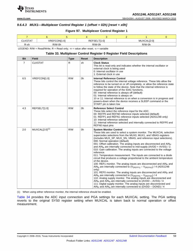
59
ADS1246, ADS1247, ADS1248www.ti.com SBAS426H –AUGUST 2008–REVISED MARCH 2016
Product Folder Links: ADS1246 ADS1247 ADS1248
Submit Documentation FeedbackCopyright © 2008–2016, Texas Instruments Incorporated
9.6.4.3 MUX1—Multiplexer Control Register 1 (offset = 02h) [reset = x0h]
Figure 97. Multiplexer Control Register 1
7 6 5 4 3 2 1 0CLKSTAT VREFCON[1:0] REFSELT[1:0] MUXCAL[2:0]
R-xh R/W-0h R/W-0h R/W-0hLEGEND: R/W = Read/Write; R = Read only; -n = value after reset; -x = variable
(1) When using either reference monitor, the internal reference should be enabled.
Table 33. Multiplexer Control Register 0 Register Field DescriptionsBit Field Type Reset Description7 CLKSTAT R xh Clock Status
This bit is read-only and indicates whether the internal oscillator orexternal clock is being used0: Internal oscillator in use1: External clock in use
6:5 VREFCON[1:0] R/W 0h Internal Reference ControlThese bits control the internal voltage reference. These bits allow thereference to be turned on or off completely, or allow the reference stateto follow the state of the device. Note that the internal reference isrequired for operation of the IDAC functions.00: Internal reference is always off (default)01: Internal reference is always on10 or 11: Internal reference is on when a conversion is in progress andpowers-down when the device receives a SLEEP command or theSTART pin is taken low
4:3 REFSELT[1:0] R/W 0h Reference Select ControlThese bits select the reference input for the ADC.00: REFP0 and REFN0 reference inputs selected (default)01: REFP1 and REFN1 reference inputs selected (ADS1248 only)10: Internal reference selected11: Internal reference selected and internally connected to REFP0 andREFN0 input pins
2:0 MUXCAL[2:0] (1) R/W 0h System Monitor ControlThese bits are used to select a system monitor. The MUXCAL selectionsupercedes selections from the MUX0, MUX1, and VBIAS registers(includes MUX_SP, MUX_SN, VBIAS, and reference input selections).000: Normal operation (default)001: Offset calibration. The analog inputs are disconnected and AINPand AINN are internally connected to mid-supply (AVDD + AVSS) / 2.010: Gain calibration. The analog inputs are connected to the voltagereference.011: Temperature measurement. The inputs are connected to a diodecircuit that produces a voltage proportional to the ambient temperatureof the device.100: REF1 monitor. The analog inputs are disconnected and AINP andAINN are internally connected to (V(REFP1) – V(REFN1)) / 4 (ADS1248only)101: REF0 monitor. The analog inputs are disconnected and AINP andAINN are internally connected to (V(REFP0) – V(REFN0)) / 4110: Analog supply monitor. The analog inputs are disconnected andAINP and AINN are internally connected to (AVDD – AVSS) / 4111: Digital supply monitor. The analog inputs are disconnected andAINP and AINN are internally connected to (DVDD – DGND) / 4
Table 34 provides the ADC input connection and PGA settings for each MUXCAL setting. The PGA settingreverts to the original SYS0 register setting when MUXCAL is taken back to normal operation or offsetmeasurement.

60
ADS1246, ADS1247, ADS1248SBAS426H –AUGUST 2008–REVISED MARCH 2016 www.ti.com
Product Folder Links: ADS1246 ADS1247 ADS1248
Submit Documentation Feedback Copyright © 2008–2016, Texas Instruments Incorporated
Table 34. MUXCAL SettingsMUXCAL[2:0] PGA GAIN SETTING ADC INPUT
000 Set by SYS0 register Normal operation001 Set by SYS0 register Inputs shorted to mid-supply (AVDD + AVSS) / 2010 Forced to 1 V(REFP) – V(REFN) (full-scale)011 Forced to 1 Temperature measurement diode100 Forced to 1 (V(REFP1) – V(REFN1)) / 4101 Forced to 1 (V(REFP0) – V(REFN0)) / 4110 Forced to 1 (AVDD – AVSS) / 4111 Forced to 1 (DVDD – DGND) / 4
9.6.4.4 SYS0—System Control Register 0 (offset = 03h) [reset = 00h]
Figure 98. System Control Register 0
7 6 5 4 3 2 1 00 PGA[2:0] DR[3:0]
R-0h R/W-0h R/W-0hLEGEND: R/W = Read/Write; R = Read only; -n = value after reset; -x = variable
Table 35. System Control Register 0 Field DescriptionsBit Field Type Reset Description7 RESERVED R 0h Reserved
This bit must always be set to 06:4 PGA[2:0] R/W 0h Gain Setting for PGA
These bits determine the gain of the PGA000: PGA = 1 (default)001: PGA = 2010: PGA = 4011: PGA = 8100: PGA = 16101: PGA = 32110: PGA = 64111: PGA = 128
3:0 DR[3:0] R/W 0h Data Output Rate SettingThese bits determine the data output rate of the ADC0000: DR = 5 SPS (default)0001: DR = 10 SPS0010: DR = 20 SPS0011: DR = 40 SPS0100: DR = 80 SPS0101: DR = 160 SPS0110: DR = 320 SPS0111: DR = 640 SPS1000: DR = 1000 SPS1001 to 1111: DR = 2000 SPS

61
ADS1246, ADS1247, ADS1248www.ti.com SBAS426H –AUGUST 2008–REVISED MARCH 2016
Product Folder Links: ADS1246 ADS1247 ADS1248
Submit Documentation FeedbackCopyright © 2008–2016, Texas Instruments Incorporated
9.6.4.5 OFC—Offset Calibration Coefficient Register (offset = 04h, 05h, 06h) [reset = 00h, 00h, 00h]These bits make up the offset calibration coefficient register of the ADS1247 and ADS1248.
Figure 99. Offset Calibration Coefficient Register
7 6 5 4 3 2 1 0OFC[7:0]R/W-00h
15 14 13 12 11 10 9 8OFC[15:8]R/W-00h
23 22 21 20 19 18 17 16OFC[23:16]
R/W-00h
LEGEND: R/W = Read/Write; R = Read only; -n = value after reset; -x = variable
Table 36. Offset Calibration Coefficient Register Field DescriptionsBit Field Type Reset Description
23:0 OFC[23:0] R/W 000000h Offset Calibration RegisterThree registers compose the ADC 24-bit offset calibration word.The 24-bit word is twos complement format and is internally left-shifted to align with the ADC 24-bit conversion result. The ADCsubtracts the register value from the conversion result before fullscale operation.
9.6.4.6 FSC—Full-Scale Calibration Coefficient Register (offset = 07h, 08h, 09h) [reset = PGA dependent]These bits make up the full-scale calibration coefficient register. The reset value for FSC is factory-trimmed foreach PGA setting. The factory-trimmed FSC reset value is automatically loaded whenever the PGA setting ischanged.
Figure 100. Full-Scale Calibration Coefficient Register
7 6 5 4 3 2 4 0FSC[7:0]R/W-xxh
15 14 13 12 11 10 9 8FSC[15:8]R/W-xxh
23 22 21 20 19 18 17 16FSC[23:16]
R/W-xxh
LEGEND: R/W = Read/Write; R = Read only; -n = value after reset; -x = variable
Table 37. Full-Scale Calibration Coefficient Register Field DescriptionsBit Field Type Reset Description
23:0 FSC[23:0] R/W xxxxxxh Full-Scale Calibration RegisterThree registers compose the ADC 24-bit full-scale calibrationword. The 24-bit word is straight binary. The ADC divides theregister value by the FSC register by 400000h to derive thescale factor for calibration. After the offset calibration, the ADCmultiplies the scale factor by the conversion result. The factory-trimmed FSC reset value is automatically loaded whenever thePGA setting is changed.

62
ADS1246, ADS1247, ADS1248SBAS426H –AUGUST 2008–REVISED MARCH 2016 www.ti.com
Product Folder Links: ADS1246 ADS1247 ADS1248
Submit Documentation Feedback Copyright © 2008–2016, Texas Instruments Incorporated
9.6.4.7 IDAC0—IDAC Control Register 0 (offset = 0Ah) [reset = x0h]
Figure 101. IDAC Control Register 0
7 6 5 4 3 2 1 0ID[3:0] DRDY MODE IMAG[2:0]R-xh R/W-0h R/W-0h
LEGEND: R/W = Read/Write; R = Read only; -n = value after reset; -x = variable
(1) Cannot be used in SDATAC mode
Table 38. IDAC Control Register 0 Field DescriptionsBit Field Type Reset Description7:4 ID[3:0] R xh Revision Identification
Read-only, factory-programmed bits; used for revisionidentification.
3 DRDY MODE R/W 0h Data Ready Mode SettingThis bit sets the DOUT/DRDY pin functionality. In either settingof the DRDY MODE bit, the dedicated DRDY pin continues toindicate data ready, active low.0: DOUT/DRDY pin functions only as Data Out (default)1: DOUT/DRDY pin functions both as Data Out and Data Ready,active low (1)
2:0 IMAG[2:0] R/W 0h IDAC Excitation Current MagnitudeThe ADS1247 and ADS1248 have two excitation currentsources (IDACs) that can be used for sensor excitation. TheIMAG bits control the magnitude of the excitation current. TheIDACs require the internal reference to be on.000: off (default)001: 50 μA010: 100 μA011: 250 μA100: 500 μA101: 750 μA110: 1000 μA111: 1500 μA

63
ADS1246, ADS1247, ADS1248www.ti.com SBAS426H –AUGUST 2008–REVISED MARCH 2016
Product Folder Links: ADS1246 ADS1247 ADS1248
Submit Documentation FeedbackCopyright © 2008–2016, Texas Instruments Incorporated
9.6.4.8 IDAC1—IDAC Control Register 1 (offset = 0Bh) [reset = FFh]
Figure 102. IDAC Control Register 1 (ADS1247)
7 6 5 4 3 2 1 01 1 I1DIR[1:0] 1 1 I2DIR[1:0]
R-1h R-1h R/W-3h R-1h R-1h R/W-3hLEGEND: R/W = Read/Write; R = Read only; -n = value after reset; -x = variable
Figure 103. IDAC Control Register 1 (ADS1248)
7 6 5 4 3 2 1 0I1DIR[3:0] I2DIR[3:0]R/W-Fh R/W-Fh
LEGEND: R/W = Read/Write; R = Read only; -n = value after reset; -x = variable
The two IDACs on the ADS1248 can be routed to either the IEXC1 and IEXC2 output pins or directly to theanalog inputs.
Table 39. IDAC Control Register Field DescriptionsBit Field Type Reset Description7:4 I1DIR[3:0] R/W Fh IDAC Excitation Current Output 1
These bits select the output pin for the first excitation currentsource0000: AIN00001: AIN10010: AIN20011: AIN30100: AIN4 (ADS1248 only)0101: AIN5 (ADS1248 only)0110: AIN6 (ADS1248 only)0111: AIN7 (ADS1248 only)10x0: IEXC1 (ADS1248 only)10x1: IEXC2 (ADS1248 only)11xx: Disconnected (default)
3:0 I2DIR[3:0] R/W Fh IDAC Excitation Current Output 2These bits select the output pin for the second excitation currentsource0000: AIN00001: AIN10010: AIN20011: AIN30100: AIN4 (ADS1248 only)0101: AIN5 (ADS1248 only)0110: AIN6 (ADS1248 only)0111: AIN7 (ADS1248 only)10x0: IEXC1 (ADS1248 only)10x1: IEXC2 (ADS1248 only)11xx: Disconnected (default)
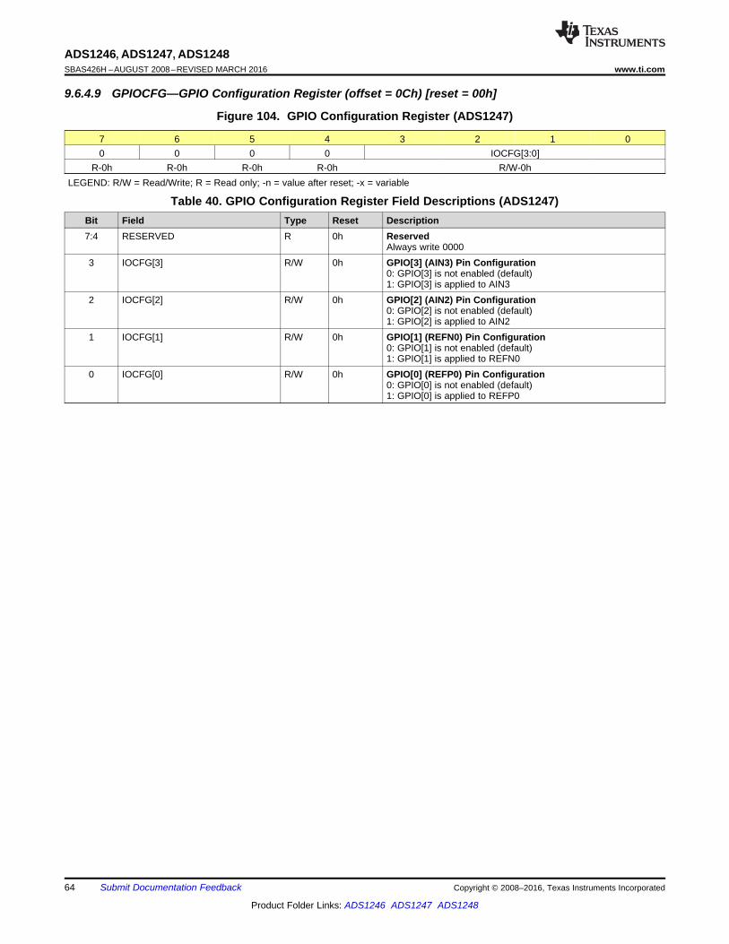
64
ADS1246, ADS1247, ADS1248SBAS426H –AUGUST 2008–REVISED MARCH 2016 www.ti.com
Product Folder Links: ADS1246 ADS1247 ADS1248
Submit Documentation Feedback Copyright © 2008–2016, Texas Instruments Incorporated
9.6.4.9 GPIOCFG—GPIO Configuration Register (offset = 0Ch) [reset = 00h]
Figure 104. GPIO Configuration Register (ADS1247)
7 6 5 4 3 2 1 00 0 0 0 IOCFG[3:0]
R-0h R-0h R-0h R-0h R/W-0hLEGEND: R/W = Read/Write; R = Read only; -n = value after reset; -x = variable
Table 40. GPIO Configuration Register Field Descriptions (ADS1247)Bit Field Type Reset Description7:4 RESERVED R 0h Reserved
Always write 00003 IOCFG[3] R/W 0h GPIO[3] (AIN3) Pin Configuration
0: GPIO[3] is not enabled (default)1: GPIO[3] is applied to AIN3
2 IOCFG[2] R/W 0h GPIO[2] (AIN2) Pin Configuration0: GPIO[2] is not enabled (default)1: GPIO[2] is applied to AIN2
1 IOCFG[1] R/W 0h GPIO[1] (REFN0) Pin Configuration0: GPIO[1] is not enabled (default)1: GPIO[1] is applied to REFN0
0 IOCFG[0] R/W 0h GPIO[0] (REFP0) Pin Configuration0: GPIO[0] is not enabled (default)1: GPIO[0] is applied to REFP0

65
ADS1246, ADS1247, ADS1248www.ti.com SBAS426H –AUGUST 2008–REVISED MARCH 2016
Product Folder Links: ADS1246 ADS1247 ADS1248
Submit Documentation FeedbackCopyright © 2008–2016, Texas Instruments Incorporated
Figure 105. GPIO Configuration Register (ADS1248)
7 6 5 4 3 2 1 0IOCFG[7:0]
R/W-00hLEGEND: R/W = Read/Write; R = Read only; -n = value after reset; -x = variable
Table 41. GPIO Configuration Register Field Descriptions (ADS1248)Bit Field Type Reset Description7 IOCFG[7] R/W 0h GPIO[7] (AIN7) Pin Configuration
0: GPIO[7] is not enabled (default)1: GPIO[7] is applied to AIN7
6 IOCFG[6] R/W 0h GPIO[6] (AIN6) Pin Configuration0: GPIO[6] is not enabled (default)1: GPIO[6] is applied to AIN6
5 IOCFG[5] R/W 0h GPIO[5] (AIN5) Pin Configuration0: GPIO[5] is not enabled (default)1: GPIO[5] is applied to AIN5
4 IOCFG[4] R/W 0h GPIO[4] (AIN4) Pin Configuration0: GPIO[4] is not enabled (default)1: GPIO[4] is applied to AIN4
3 IOCFG[3] R/W 0h GPIO[3] (AIN3) Pin Configuration0: GPIO[3] is not enabled (default)1: GPIO[3] is applied to AIN3
2 IOCFG[2] R/W 0h GPIO[2] (AIN2) Pin Configuration0: GPIO[2] is not enabled (default)1: GPIO[2] is applied to AIN2
1 IOCFG[1] R/W 0h GPIO[1] (REFN0) Pin Configuration0: GPIO[1] is not enabled (default)1: GPIO[1] is applied to REFN0
0 IOCFG[0] R/W 0h GPIO[0] (REFP0) Pin Configuration0: GPIO[0] is not enabled (default)1: GPIO[0] is applied to REFP0

66
ADS1246, ADS1247, ADS1248SBAS426H –AUGUST 2008–REVISED MARCH 2016 www.ti.com
Product Folder Links: ADS1246 ADS1247 ADS1248
Submit Documentation Feedback Copyright © 2008–2016, Texas Instruments Incorporated
9.6.4.10 GPIODIR—GPIO Direction Register (offset = 0Dh) [reset = 00h]
Figure 106. GPIO Direction Register (ADS1247)
7 6 5 4 3 2 1 00 0 0 0 IODIR[3:0]
R-0h R-0h R-0h R-0h R/W-0hLEGEND: R/W = Read/Write; R = Read only; -n = value after reset; -x = variable
Table 42. GPIO Direction Register Field Descriptions (ADS1247)Bit Field Type Reset Description7:4 RESERVED R 0h Reserved
Always write 00003 IODIR[3] R/W 0h GPIO[3] (AIN3) Pin Direction
Configures GPIO[3] as a GPIO input or GPIO output0: GPIO[3] is an output (default)1: GPIO[3] is an input
2 IODIR[2] R/W 0h GPIO[2] (AIN2) Pin DirectionConfigures GPIO[2] as a GPIO input or GPIO output0: GPIO[2] is an output (default)1: GPIO[2] is an input
1 IODIR[1] R/W 0h GPIO[1] (REFN0) Pin DirectionConfigures GPIO[1] as a GPIO input or GPIO output0: GPIO[1] is an output (default)1: GPIO[1] is an input
0 IODIR[0] R/W 0h GPIO[0] (REFP0) Pin DirectionConfigures GPIO[0] as a GPIO input or GPIO output0: GPIO[0] is an output (default)1: GPIO[0] is an input

67
ADS1246, ADS1247, ADS1248www.ti.com SBAS426H –AUGUST 2008–REVISED MARCH 2016
Product Folder Links: ADS1246 ADS1247 ADS1248
Submit Documentation FeedbackCopyright © 2008–2016, Texas Instruments Incorporated
Figure 107. GPIO Direction Register (ADS1248)
7 6 5 4 3 2 1 0IODIR[7:0]R/W-00h
LEGEND: R/W = Read/Write; R = Read only; -n = value after reset; -x = variable
Table 43. GPIO Direction Register Field Descriptions (ADS1248)Bit Field Type Reset Description7 IODIR[7] R/W 0h GPIO[7] (AIN7) Pin Direction
Configures GPIO[7] as a GPIO input or GPIO output0: GPIO[7] is an output (default)1: GPIO[7] is an input
6 IODIR[6] R/W 0h GPIO[6] (AIN6) Pin DirectionConfigures GPIO[6] as a GPIO input or GPIO output0: GPIO[6] is an output (default)1: GPIO[6] is an input
5 IODIR[5] R/W 0h GPIO[5] (AIN5) Pin DirectionConfigures GPIO[5] as a GPIO input or GPIO output0: GPIO[5] is an output (default)1: GPIO[5] is an input
4 IODIR[4] R/W 0h GPIO[4] (AIN4) Pin DirectionConfigures GPIO[4] as a GPIO input or GPIO output0: GPIO[4] is an output (default)1: GPIO[4] is an input
3 IODIR[3] R/W 0h GPIO[3] (AIN3) Pin DirectionConfigures GPIO[3] as a GPIO input or GPIO output0: GPIO[3] is an output (default)1: GPIO[3] is an input
2 IODIR[2] R/W 0h GPIO[2] (AIN2) Pin DirectionConfigures GPIO[2] as a GPIO input or GPIO output0: GPIO[2] is an output (default)1: GPIO[2] is an input
1 IODIR[1] R/W 0h GPIO[1] (REFN0) Pin DirectionConfigures GPIO[1] as a GPIO input or GPIO output0: GPIO[1] is an output (default)1: GPIO[1] is an input
0 IODIR[0] R/W 0h GPIO[0] (REFP0) Pin DirectionConfigures GPIO[0] as a GPIO input or GPIO output0: GPIO[0] is an output (default)1: GPIO[0] is an input

68
ADS1246, ADS1247, ADS1248SBAS426H –AUGUST 2008–REVISED MARCH 2016 www.ti.com
Product Folder Links: ADS1246 ADS1247 ADS1248
Submit Documentation Feedback Copyright © 2008–2016, Texas Instruments Incorporated
9.6.4.11 GPIODAT—GPIO Data Register (offset = 0Eh) [reset = 00h]
Figure 108. GPIO Data Register (ADS1247)
7 6 5 4 3 2 1 00 0 0 0 IODAT[3:0]
R-0h R-0h R-0h R-0h R/W-0hLEGEND: R/W = Read/Write; R = Read only; -n = value after reset; -x = variable
Table 44. GPIO Data Register Field Descriptions (ADS1247)Bit Field Type Reset Description7:4 RESERVED R 0h Reserved
Always write 00003 IODAT[3] R/W 0h GPIO[3] (AIN3) Pin Data
Configured as an output, read returns the register valueConfigured as an input, write sets the register value only0: GPIO[3] is low (default)1: GPIO[3] is high
2 IODAT[2] R/W 0h GPIO[2] (AIN2) Pin DataConfigured as an output, read returns the register valueConfigured as an input, write sets the register value only0: GPIO[2] is low (default)1: GPIO[2] is high
1 IODAT[1] R/W 0h GPIO[1] (REFN0) Pin DataConfigured as an output, read returns the register valueConfigured as an input, write sets the register value only0: GPIO[1] is low (default)1: GPIO[1] is high
0 IODAT[0] R/W 0h GPIO[0] (REFP0) Pin DataConfigured as an output, read returns the register valueConfigured as an input, write sets the register value only0: GPIO[0] is low (default)1: GPIO[0] is high

69
ADS1246, ADS1247, ADS1248www.ti.com SBAS426H –AUGUST 2008–REVISED MARCH 2016
Product Folder Links: ADS1246 ADS1247 ADS1248
Submit Documentation FeedbackCopyright © 2008–2016, Texas Instruments Incorporated
Figure 109. GPIO Data Register (ADS1248)
7 6 5 4 3 2 1 0IODAT[7:0]R/W-00h
LEGEND: R/W = Read/Write; R = Read only; -n = value after reset; -x = variable
Table 45. GPIO Data Register Field Descriptions (ADS1248)Bit Field Type Reset Description7 IODAT[7] R/W 0h GPIO[7] (AIN7) Pin Data
Configured as an output, read returns the register valueConfigured as an input, write sets the register value only0: GPIO[7] is low (default)1: GPIO[7] is high
6 IODAT[6] R/W 0h GPIO[6] (AIN6) Pin DataConfigured as an output, read returns the register valueConfigured as an input, write sets the register value only0: GPIO[6] is low (default)1: GPIO[6] is high
5 IODAT[5] R/W 0h GPIO[5] (AIN5) Pin DataConfigured as an output, read returns the register valueConfigured as an input, write sets the register value only0: GPIO[5] is low (default)1: GPIO[5] is high
4 IODAT[4] R/W 0h GPIO[4] (AIN4) Pin DataConfigured as an output, read returns the register valueConfigured as an input, write sets the register value only0: GPIO[4] is low (default)1: GPIO[4] is high
3 IODAT[3] R/W 0h GPIO[3] (AIN3) Pin DataConfigured as an output, read returns the register valueConfigured as an input, write sets the register value only0: GPIO[3] is low (default)1: GPIO[3] is high
2 IODAT[2] R/W 0h GPIO[2] (AIN2) Pin DataConfigured as an output, read returns the register valueConfigured as an input, write sets the register value only0: GPIO[2] is low (default)1: GPIO[2] is high
1 IODAT[1] R/W 0h GPIO[1] (REFN0) Pin DataConfigured as an output, read returns the register valueConfigured as an input, write sets the register value only0: GPIO[1] is low (default)1: GPIO[1] is high
0 IODAT[0] R/W 0h GPIO[0] (REFP0) Pin DataConfigured as an output, read returns the register valueConfigured as an input, write sets the register value only0: GPIO[0] is low (default)1: GPIO[0] is high

1
2
3
4
5
6
7
8
9
10
11
12
13
14
28
27
26
25
24
23
22
21
20
19
18
17
16
15
DVDD
DGND
CLK
RESET
REFP0
REFN0
REFP1
REFN1
VREFOUT
VREFCOM
AIN0
AIN1
AIN4
AIN5
SCLK
DIN
DOUT/DRDY
DRDY
CS
START
AVDD
AVSS
IEXC1
IEXC2
AIN0
AIN1
AIN7
AIN6
47
0.1 PF
0.1 PF
47
47
47
47
47
47
GPIO
SCLK
DIN
DOUT
GPIO/IRQ
GPIO
GPIO
Microcontrollerwith SPI
Device
1 PF
3.3 V
5 V
DVDD
DVSS0.1 PF
3.3 V
70
ADS1246, ADS1247, ADS1248SBAS426H –AUGUST 2008–REVISED MARCH 2016 www.ti.com
Product Folder Links: ADS1246 ADS1247 ADS1248
Submit Documentation Feedback Copyright © 2008–2016, Texas Instruments Incorporated
10 Application and Implementation
NOTEInformation in the following applications sections is not part of the TI componentspecification, and TI does not warrant its accuracy or completeness. TI’s customers areresponsible for determining suitability of components for their purposes. Customers shouldvalidate and test their design implementation to confirm system functionality.
10.1 Application InformationThe ADS1246, ADS1247, and ADS1248 make up a family of precision, 24-bit, ΔΣ ADCs that offers manyintegrated features to ease the measurement of the most common sensor types including various types oftemperature and bridge sensors. Primary considerations when designing an application with these devicesinclude connecting and configuring the serial interface, designing the analog input filtering, establishing anappropriate external reference for ratiometric measurements, and setting the common-mode input voltage for theinternal PGA. These considerations are discussed in the following sections.
10.1.1 Serial Interface ConnectionsThe principle serial interface connections for the ADS1248 are shown in Figure 110.
Figure 110. Serial Interface Connections
Most microcontroller SPI peripherals can operate with the ADS1248. The interface operates in SPI mode 1where CPOL = 0 and CPHA = 1. In SPI mode 1, SCLK idles low and data are launched or changed only onSCLK rising edges; data are latched or read by the master and slave on SCLK falling edges. Details of the SPIcommunication protocol employed by the device can be found in the Serial Interface Timing Requirementssection.
TI recommends placing 47-Ω resistors in series with all digital input and output pins (CS, SCLK, DIN,DOUT/DRDY, DRDY, RESET and START). This resistance smooths sharp transitions, suppresses overshoot,and offers some overvoltage protection. Care must be taken to meet all SPI timing requirements because theadditional resistors interact with the bus capacitances present on the digital signal lines.
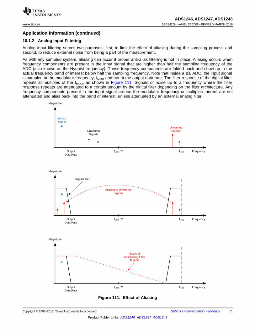
Magnitude
fMOD / 2 fMODOutputData Rate
Frequency
ExternalAntialiasing Filter
Roll-Off
Magnitude
fMOD / 2 fMODOutputData Rate
Frequency
Digital Filter
Magnitude
fMOD / 2 fMODOutputData Rate
Frequency
SensorSignal
Unwanted Signals
Unwanted Signals
Aliasing of Unwanted Signals
71
ADS1246, ADS1247, ADS1248www.ti.com SBAS426H –AUGUST 2008–REVISED MARCH 2016
Product Folder Links: ADS1246 ADS1247 ADS1248
Submit Documentation FeedbackCopyright © 2008–2016, Texas Instruments Incorporated
Application Information (continued)10.1.2 Analog Input FilteringAnalog input filtering serves two purposes: first, to limit the effect of aliasing during the sampling process andsecond, to reduce external noise from being a part of the measurement.
As with any sampled system, aliasing can occur if proper anti-alias filtering is not in place. Aliasing occurs whenfrequency components are present in the input signal that are higher than half the sampling frequency of theADC (also known as the Nyquist frequency). These frequency components are folded back and show up in theactual frequency band of interest below half the sampling frequency. Note that inside a ΔΣ ADC, the input signalis sampled at the modulator frequency, fMOD and not at the output data rate. The filter response of the digital filterrepeats at multiples of the fMOD, as shown in Figure 111. Signals or noise up to a frequency where the filterresponse repeats are attenuated to a certain amount by the digital filter depending on the filter architecture. Anyfrequency components present in the input signal around the modulator frequency or multiples thereof are notattenuated and alias back into the band of interest, unless attenuated by an external analog filter.
Figure 111. Effect of Aliasing

72
ADS1246, ADS1247, ADS1248SBAS426H –AUGUST 2008–REVISED MARCH 2016 www.ti.com
Product Folder Links: ADS1246 ADS1247 ADS1248
Submit Documentation Feedback Copyright © 2008–2016, Texas Instruments Incorporated
Application Information (continued)Many sensor signals are inherently bandlimited; for example, the output of a thermocouple has a limited rate ofchange. In this case, the sensor signal does not alias back into the pass-band when using a ΔΣ ADC. However,any noise pick-up along the sensor wiring or the application circuitry can potentially alias into the pass-band.Power line-cycle frequency and harmonics are one common noise source. External noise can also be generatedfrom electromagnetic interference (EMI) or radio frequency interference (RFI) sources, such as nearby motorsand cellular phones. Another noise source typically exists on the printed circuit board (PCB) itself in the form ofclocks and other digital signals. Analog input filtering helps remove unwanted signals from affecting themeasurement result.
A first-order resistor-capacitor (RC) filter is (in most cases) sufficient to either totally eliminate aliasing, or toreduce the effect of aliasing to a level within the noise floor of the sensor. Ideally, any signal beyond fMOD/2 isattenuated to a level below the noise floor of the ADC. The digital filter of the ADS1248 attenuates signals to acertain degree, as illustrated in the filter response plots in the Digital Filter section. In addition, noise componentsare usually smaller in magnitude than the actual sensor signal. Therefore, using a first-order RC filter with acutoff frequency set at the output data rate or 10x higher is generally a good starting point for a system design.
Internal to the device, prior to the PGA inputs, is an EMI filter; see Figure 52. The cutoff frequency of this filter isapproximately 47 MHz, which helps reject high-frequency interferences.
10.1.3 External Reference and Ratiometric MeasurementsThe full-scale range of the ADS1248 is defined by the reference voltage and the PGA gain (FSR = ±VREF / Gain).An external reference can be used instead of the integrated 2.048-V reference to adapt the FSR to the specificsystem needs. An external reference must be used if VIN > 2.048 V. For example, an external 2.5-V reference isrequired in order to measure signals as large as 2.5 V. Note that the input signal must be within the common-mode input range to be valid, and that the reference input voltage must be between 0.5 V and (AVDD – AVSS –1 V).
The buffered reference inputs of the device also allow the implementation of ratiometric measurements. In aratiometric measurement the same excitation source that is used to excite the sensor is also used to establishthe reference for the ADC. As an example, a simple form of a ratiometric measurement uses the same currentsource to excite both the resistive sensor element (such as an RTD) and another resistive reference element thatis in series with the element being measured. The voltage that develops across the reference element is used asthe reference source for the ADC. In this configuration, current noise and drift are common to both the sensormeasurement and the reference, therefore these components cancel out in the ADC transfer function. The outputcode is only a ratio of the sensor element value and the reference resistor value, and is not affected by theabsolute value of the excitation current.
10.1.4 Establishing a Proper Common-Mode Input VoltageThe ADS1248 is used to measure various types of signal configurations. However, configuring the input of thedevice properly for the respective signal type is important.
The ADS1248 features an 8-input multiplexer (while the ADS1247 has a 4-input multiplexer). Each input can beindependently selected as the positive input or the negative input to be measured by the ADC. With an 8-inputmultiplexer, the user can measure four independent differential-input channels. The user can also choose tomeasure 7 channels, using one input as a fixed common input. Regardless of the analog input configuration,make sure that all inputs, including the common input are within the common-mode input voltage range.
If the supply is unipolar (e.g. AVSS = 0 V and AVDD = 5 V), then V(AINN) = 0 V is not within the common-modeinput range as shown by Equation 3. Therefore, a single-ended measurement with the common input connectedto ground is not possible. TI recommends connecting the common-input to mid-supply or alternatively toVREFOUT. Note that the common-mode range becomes further restricted with increasing PGA gain.
If the supply is bipolar (AVSS = –2.5 V and AVDD = 2.5 V), then ground is within the common-mode input range.Single-ended measurements with the common input connected to 0 V are possible in this case.
For a detailed explanation of the common-mode input range as it relates to the PGA see the PGA Common-Mode Voltage Requirements section.

73
ADS1246, ADS1247, ADS1248www.ti.com SBAS426H –AUGUST 2008–REVISED MARCH 2016
Product Folder Links: ADS1246 ADS1247 ADS1248
Submit Documentation FeedbackCopyright © 2008–2016, Texas Instruments Incorporated
Application Information (continued)10.1.5 Isolated (or Floating) Sensor InputsIsolated sensors (sensors that are not referenced to the ADC ground) must have a common-mode voltageestablished within the specified ADC input range. Level shift the common-mode voltage by external resistorbiasing, by connecting the negative lead to ground (bipolar analog supply), or by connecting to a dc voltage(unipolar analog supply). The 2.048-V reference output voltage may also be used to provide level shifting tofloating sensor inputs.
10.1.6 Unused Inputs and OutputsTo minimize leakage currents on the analog inputs, leave unused analog inputs floating, connect them to mid-supply, or connect them to AVDD. Connecting unused analog inputs to AVSS is possible as well, but can yieldhigher leakage currents than the options mentioned before.
Do not float unused digital inputs or excessive power-supply leakage current may result. Tie all unused digitalinputs to the appropriate levels, DVDD or DGND, including when in power-down mode. If the DRDY output is notused, leave the pin unconnected or tie it to DVDD using a weak pull-up resistor.
10.1.7 Pseudo Code ExampleThe following list shows a pseudo code sequence with the required steps to set up the device and themicrocontroller that interfaces to the ADC in order to take subsequent readings from the ADS1248 in stop readdata continuous (SDATAC) mode. In SDATAC mode, it is sufficient to wait for a time period longer than the datarate to retrieve the conversion result. New conversion data will not interrupt the reading of registers or data onDOUT. However in this example, the dedicated DRDY pin is used to indicate availability of new conversion datainstead of waiting a set time period for a readout. The default configuration register settings are changed to PGAgain = 16, using the internal reference, and a data rate of 20 SPS.
Power up;Delay for a minimum of 16 ms to allow power supplies to settle and power-on reset to complete;Enable the device by setting the START pin high;Configure the serial interface of the microcontroller to SPI mode 1 (CPOL = 0, CPHA =1);If the CS pin is not tied low permanently, configure the microcontroller GPIO connected to CS as anoutput;Configure the microcontroller GPIO connected to the DRDY pin as a falling edge triggered interruptinput;Set CS to the device low;Delay for a minimum of tCSSC;Send the RESET command (06h) to make sure the device is properly reset after power up;Delay for a minimum of 0.6 ms;Send SDATAC command (16h) to prevent the new data from interrupting data or register transactions;Write the respective register configuration with the WREG command (40h, 03h, 01h, 00h, 03h and 42h);As an optional sanity check, read back all configuration registers with the RREG command (four bytesfrom 20h, 03h);Send the SYNC command (04h) to start the ADC conversion;Delay for a minimum of tSCCS;Clear CS to high (resets the serial interface);Loop
Wait for DRDY to transition low;Take CS low;Delay for a minimum of tCSSC;Send the RDATA command (12h);Send 24 SCLKs to read out conversion data on DOUT/DRDY;Delay for a minimum of tSCCS;Clear CS to high;
Take CS low;Delay for a minimum of tCSSC;Send the SLEEP command (02h) to stop conversions and put the device in power-down mode;

Conversion result for channel 1
WREG WREG
DVDD
START
RESET
CS
DIN
DOUT
DRDY
SCLK
Initial setting:AIN0 is the positive channel,AIN1 is the negative channel,Internal reference selected,PGA gain = 32, DR = 2 kSPS,VBIAS is connected to pins AIN1 and AIN3
tDRDY
ADC initial setupPower-up sequence
16 ms(1)
Conversion result for channel 2
NOP
Multiplexer change to channel 2 Data retrieval for channel 2 conversion
0.513 ms for MUX0 write
AIN2 is the positive channel,AIN3 is the negative channel.
74
ADS1246, ADS1247, ADS1248SBAS426H –AUGUST 2008–REVISED MARCH 2016 www.ti.com
Product Folder Links: ADS1246 ADS1247 ADS1248
Submit Documentation Feedback Copyright © 2008–2016, Texas Instruments Incorporated
Application Information (continued)10.1.8 Channel Multiplexing ExampleThis example applies only to the ADS1247 and ADS1248. It explains a method to use the device with twosensors connected to two different analog channels. Figure 112 shows the sequence of SPI operationsperformed on the device. After power up, 216 tCLK cycles are required before communication can be started.During the first 216 tCLK cycles, the device is internally held in a reset state. In this example, one of the sensors isconnected to channels AIN0 and AIN1 and the other sensor is connected to channels AIN2 and AIN3. The ADCis operated at a data rate of 2 kSPS. The PGA gain is set to 32 for both sensors. VBIAS is connected to thenegative terminal of both sensors (that is, channels AIN1 and AIN3). All these settings can be changed byperforming a block write operation on the first four registers of the device. After the DRDY pin goes low, theconversion result can be immediately retrieved by sending in 24 SCLK pulses because the device defaults toRDATAC mode. As the conversion result is being retrieved, the active input channels can be switched to AIN2and AIN3 by writing into the MUX0 register in a full-duplex manner, as shown in Figure 112. The write operationis completed with an additional eight SCLK pulses. The time from the write operation into the MUX0 register tothe next DRDY low transition is shown in Figure 112 and is 0.513 ms in this case. After DRDY goes low, theconversion result can be retrieved and the active channel can be switched as before.
(1) For fCLK = 4.096 MHz.
Figure 112. SPI Communication Sequence for Channel Multiplexing

Conversion result for channel 1
WREG NOP
DVDD
START
RESET
CS
DIN
DOUT
DRDY
SCLK
ADC enterspower-down
mode
Initial setting:AIN0 is the positive channel,AIN1 is the negative channel,Internal reference selected,PGA gain = 32, DR = 2 kSPS,VBIAS is connected to AIN1
tDRDY
(0.575 ms)
ADC is put in power-down mode after a single conversion.
Data are retrieved when the ADC is powered down
ADC initial setupPower-up sequence
16 ms(1)
75
ADS1246, ADS1247, ADS1248www.ti.com SBAS426H –AUGUST 2008–REVISED MARCH 2016
Product Folder Links: ADS1246 ADS1247 ADS1248
Submit Documentation FeedbackCopyright © 2008–2016, Texas Instruments Incorporated
Application Information (continued)10.1.9 Power-Down Mode ExampleThis second example deals with performing one conversion after power up and then entering power-down mode.In this example, a sensor is connected to input channels AIN0 and AIN1. Commands to set up the device mustoccur at least 216 system clock cycles after powering up the device. The ADC operates at a data rate of 2 kSPS.The PGA gain is set to 32. VBIAS is connected to the negative terminal of the sensor (that is, channel AIN1). Allthese settings can be changed by performing a block write operation on the first four registers of the device. Afterperforming the block write operation, the START pin can be taken low. The device enters the power-down modeas soon as DRDY goes low 0.575 ms after writing into the SYS0 register. The conversion result can be retrievedeven after the device enters power-down mode by sending 24 SCLK pulses.
(1) For fCLK = 4.096 MHz.
Figure 113. SPI Communication Sequence for Entering Power-Down Mode After a Conversion
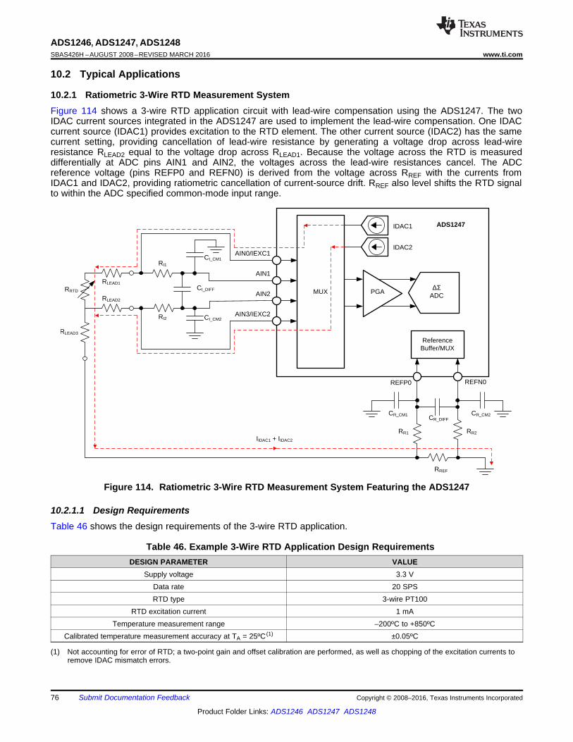
REFP0 REFN0
MUX
AIN0/IEXC1
AIN1
AIN2
AIN3/IEXC2
PGAû
ADC
ReferenceBuffer/MUX
RREF
RRTD
ADS1247
RI1
RI2
CI_CM1
CI_DIFF
CI_CM2
CR_CM1 CR_CM2CR_DIFF
RR1 RR2
IDAC1
IDAC2
RLEAD3
RLEAD1
RLEAD2
IIDAC1 + IIDAC2
76
ADS1246, ADS1247, ADS1248SBAS426H –AUGUST 2008–REVISED MARCH 2016 www.ti.com
Product Folder Links: ADS1246 ADS1247 ADS1248
Submit Documentation Feedback Copyright © 2008–2016, Texas Instruments Incorporated
(1) Not accounting for error of RTD; a two-point gain and offset calibration are performed, as well as chopping of the excitation currents toremove IDAC mismatch errors.
10.2 Typical Applications
10.2.1 Ratiometric 3-Wire RTD Measurement SystemFigure 114 shows a 3-wire RTD application circuit with lead-wire compensation using the ADS1247. The twoIDAC current sources integrated in the ADS1247 are used to implement the lead-wire compensation. One IDACcurrent source (IDAC1) provides excitation to the RTD element. The other current source (IDAC2) has the samecurrent setting, providing cancellation of lead-wire resistance by generating a voltage drop across lead-wireresistance RLEAD2 equal to the voltage drop across RLEAD1. Because the voltage across the RTD is measureddifferentially at ADC pins AIN1 and AIN2, the voltages across the lead-wire resistances cancel. The ADCreference voltage (pins REFP0 and REFN0) is derived from the voltage across RREF with the currents fromIDAC1 and IDAC2, providing ratiometric cancellation of current-source drift. RREF also level shifts the RTD signalto within the ADC specified common-mode input range.
Figure 114. Ratiometric 3-Wire RTD Measurement System Featuring the ADS1247
10.2.1.1 Design RequirementsTable 46 shows the design requirements of the 3-wire RTD application.
Table 46. Example 3-Wire RTD Application Design RequirementsDESIGN PARAMETER VALUE
Supply voltage 3.3 VData rate 20 SPSRTD type 3-wire PT100
RTD excitation current 1 mATemperature measurement range –200ºC to +850ºC
Calibrated temperature measurement accuracy at TA = 25ºC (1) ±0.05ºC

û
ADCRRTD
RREF
IDAC1
REFP REFN
RLEAD1
RLEAD2
RLEAD3IDAC2
û
ADCRRTD
RREF
IDAC1
REFP REFN
77
ADS1246, ADS1247, ADS1248www.ti.com SBAS426H –AUGUST 2008–REVISED MARCH 2016
Product Folder Links: ADS1246 ADS1247 ADS1248
Submit Documentation FeedbackCopyright © 2008–2016, Texas Instruments Incorporated
10.2.1.2 Detailed Design Procedure
10.2.1.2.1 Topology
Figure 115 shows the basic topology of a ratiometric measurement using an RTD. Shown are the ADC with theRTD and a reference resistor RREF. There is a single current source, labeled IDAC1 which is used to excite theRTD as well as to establish a reference voltage for the ADC across RREF.
Figure 115. Example of a Ratiometric RTD Measurement
With IDAC1, the ADC measures the RTD voltage using the voltage across RREF as the reference. This will give ameasurement such that the output code is proportional to the ratio of the RTD voltage and the reference voltageas shown in Equation 21 and Equation 22.
Code ∝ VRTD / VREF (21)Code ∝ (RRTD · IIDAC1) / (RREF · IIDAC1) (22)
The currents cancel so that the equation reduces to Equation 23:Code ∝ RRTD / RREF (23)
As shown in Equation 23, the measurement depends on the resistive value of the RTD and the reference resistorRREF, but not on the IDAC1 current value. Therefore, the absolute accuracy and temperature drift of theexcitation current does not matter. This is a ratiometric measurement. As long as there is no current leakagefrom IDAC1 outside of this circuit, the measurement depends only on RRTD and RREF.
In Figure 116, the lead resistances of a 3-wire RTD are shown and another excitation current source is added,labeled IDAC2.
Figure 116. Example of Lead Wire Compensation

78
ADS1246, ADS1247, ADS1248SBAS426H –AUGUST 2008–REVISED MARCH 2016 www.ti.com
Product Folder Links: ADS1246 ADS1247 ADS1248
Submit Documentation Feedback Copyright © 2008–2016, Texas Instruments Incorporated
(1) The internal reference is required to be enabled to use the IDAC current sources.(2) To implement chopping, swap IDAC1 direction for IDAC2 direction. Set I1DIR[3:0] = 0011 and I2DIR[3:0] = 0000
With a single excitation current source, RLEAD1 adds an error to the measurement. By adding IDAC2, the secondexcitation current source is used to cancel out the error in the lead wire resistance. When adding the leadresistances and the second current source, the equation becomes:
Code ∝ (VRTD + (RLEAD1 · IIDAC1) – (RLEAD2 · IIDAC2)) / (VREF · (IIDAC1 + IIDAC2)) (24)
If the lead resistances match and the excitation currents match, then RLEAD1 = RLEAD2 and IIDAC1 = IIDAC2. Thelead wire resistances cancel out so that Equation 24 reduces to the result in Equation 25 maintaining aratiometric measurement.
Code ∝ RRTD / (2 · RREF) (25)
RLEAD3 is not part of the measurement, since it is not in the input measurement path or in the reference inputpath.
As Equation 24 shows, the two current sources must be matched to cancel the lead resistances of the RTDwires. Any mismatch in the two current sources is minimized by using the multiplexer to swap or chop the twocurrent sources between the two inputs. Taking measurements in both configurations and averaging the readingsreduces the effects of mismatched current sources. The design uses the multiplexer in the ADS1247 toimplement this chopping technique to remove the mismatch error between IDAC1 and IDAC2.
10.2.1.2.2 RTD Selection
The RTD is first chosen to be a PT100 element. The RTD resistance is defined by the Callendar-Van Dusen(CVD) equations and the resistance of the RTD is known depending on the temperature. The PT100 RTD has animpedance of 100 Ω at 0˚C and roughly 0.385 Ω of resistance change per 1˚C in temperature change. With adesired temperature measurement accuracy of 0.05˚C, this translates to a resistive measurement accuracy ofapproximately 0.01925 Ω. The RTD resistance at the low end of the temperature range of –200˚C is 18.590 Ωand the resistance at the high end of the temperature range of 850˚C is 390.48 Ω.
10.2.1.2.3 Excitation Current
For the best possible resolution, the voltage across the RTD should be made as large as possible compared tothe noise floor in the measurement. In general, measurement resolution improves with increasing excitationcurrent. However, a larger excitation current will create self-heating in the RTD, which will cause drift and error inthe measurement. The selection of excitation currents trades off resolution against sensor self-heating.
The excitation current sources in this design are selected to be 1 mA. This will maximize the value of the RTDvoltage while keeping the self-heating low. The typical range of RTD self-heating coefficients is 2.5 mW/°C forsmall, thin-film elements and 65 mW/°C for larger, wire-wound elements. With 1-mA excitation at the maximumRTD resistance value, the power dissipation in the RTD is less than 0.4 mW and will keep the measurementerrors due to self-heating to less than 0.01˚C.
As mentioned in Topology, chopping of the excitation current sources cancels mismatches between the IDACs.This technique is necessary for getting the best possible accuracy from the system. Mismatch between theexcitation current sources is a large source of error if chopping is not implemented.
The internal reference voltage must be enabled while using the IDACs, even if an external ratiometricmeasurement is used for ADC conversions.
Table 47 shows the ADS1247 register settings for setting up the internal reference and the excitation currentsources.
Table 47. Register Bit Settings for Excitation Current SourcesREGISTER (Address) BIT NAME BIT VALUES COMMENT
MUX1 (02h) (1) VREFCON[1:0] 01 Internal reference enabledMUX1 (02h) REFSELT[1:0] 00 REFP0 and REFN0 reference inputs selectedIDAC0 (0Ah) IMAG[2:0] 110 IDAC magnitude = 1 mAIDAC1 (0Bh) I1DIR[3:0] (2) 0000 IDAC1 = AIN0IDAC1 (0Bh) I2DIR[3:0] (2) 0011 IDAC2 = AIN3
79
ADS1246, ADS1247, ADS1248www.ti.com SBAS426H –AUGUST 2008–REVISED MARCH 2016
Product Folder Links: ADS1246 ADS1247 ADS1248
Submit Documentation FeedbackCopyright © 2008–2016, Texas Instruments Incorporated
10.2.1.2.4 Reference Resistor RREF
TI recommends setting the common-mode voltage of the measurement near mid-supply, this helps keep theinput within the common-mode input range of the PGA.
The reference resistor is selected to be 820 Ω. The voltage across RREF is calculated from Equation 26.VREF = RREF · (IIDAC1 + IIDAC2) = 820 Ω · 2 mA = 1.64 V (26)
With AVDD = 3.3 V, Equation 26 shows that the input voltage is just below mid-supply.
The excitation current sources operate properly to a maximum IDAC compliance voltage. Above this compliancevoltage, the current sources lose current regulation. In this example, the output voltage of the excitation currentsource is calculated from the sum of the voltages across the RTD and RREF as shown in Equation 27.
VIDAC1 MAX = RRTD MAX · IIDAC1 + (RREF · (IIDAC1 + IIDAC2)) = 0.4 V + 1.64 V = 2.04 V (27)
A compliance voltage of 3.3 V – 2.04 V = 1.26 V is sufficient for proper IDAC operation. See Figure 41 andFigure 42 in Typical Characteristics for details.
Because the voltage across RREF sets the reference voltage for the ADC, the tolerance and temperature drift ofRREF directly affect the measurement gain. A resistor with 0.02% maximum tolerance is selected.
10.2.1.2.5 PGA Setting
Because the excitation current is small to reduce self-heating, the PGA in the ADS1247 is used to amplify thesignal across the RTD to utilize the full-scale range of the ADC. Starting with the reference voltage, the ADC willbe able to measure a differential input signal range of ±1.64 V. The maximum allowable PGA gain setting isbased on the reference voltage, the maximum RTD resistance, and the excitation current.
As mentioned previously the maximum resistance of the RTD will be seen at the top range of the temperaturemeasurement at 850˚C. This will give the largest voltage measurement of the ADC. RRTD@850˚C will be 390.48 Ω.
VRTD MAX = RRTD@850˚C · IIDAC1 = 390.48 Ω · 1 mA = 390.48 mV (28)
With a reference voltage of 1.64 V, the maximum gain for the PGA, without over-ranging the ADC, is shown inEquation 29.
GainMAX = VREF / VRTD MAX = 1.64 V / 390.48 mV = 4.2 V/V (29)
Selecting a PGA gain of 4 will give a maximum measurement of 95% of the positive full-scale range. Table 48shows the register settings to set the PGA gain as well as the inputs for the ADC.
Table 48. Register Bit Settings for the Input Multiplexer and PGAREGISTER (ADDRESS) BIT NAME BIT VALUES COMMENT
MUX0 (01h) MUX_SP[2:0] 001 AINP = AIN1MUX0 (01h) MUX_SN[2:0] 010 AINN = AIN2SYS0 (03h) PGA[2:0] 010 PGA Gain = 4
10.2.1.2.6 Common-Mode Input Range
Now that the component values are selected, the common-mode input range should be verified to ensure thatthe ADC and PGA are not limited in operation. Start with the maximum input voltage, which will give the mostrestriction in the common-mode input range. At the maximum input voltage, the common-mode input voltageseen by the ADC is shown in Equation 30.
VCM = VREF + (VRTD MAX / 2) = 1.64 V + (390.48 mV / 2) = 1.835 V (30)
As mentioned in Low-Noise PGA, the common-mode input range is shown in Equation 3 and is applied toEquation 31.
AVSS + 0.1 V + (VRTD MAX · Gain) / 2 ≤ VCM ≤ AVDD – 0.1 V – (VRTD MAX · Gain) / 2 (31)
After substituting in the appropriate values, the common-mode input range can be found in Equation 32 andEquation 33.
0 V + 0.1 V + (390.48 mV · 4) / 2 ≤ VCM ≤ 3.3 V – 0.1 V – (390.48 mV · 4) / 2 (32)881 mV ≤ VCM ≤ 2.42 V (33)

80
ADS1246, ADS1247, ADS1248SBAS426H –AUGUST 2008–REVISED MARCH 2016 www.ti.com
Product Folder Links: ADS1246 ADS1247 ADS1248
Submit Documentation Feedback Copyright © 2008–2016, Texas Instruments Incorporated
Because VCM = 1.835 V is within the limits of Equation 33, the RTD measurement is within the input common-mode range of the ADC and PGA. At the RTD voltage minimum (VRTD MIN = 18.59 mV), a similar calculation canbe made to show that the input common-mode voltage will be within the range as well.
10.2.1.2.7 Input and Reference Low-Pass Filters
The differential filters chosen for this application are designed to have a –3-dB corner frequency at least 10 timeslarger than the bandwidth of the ADC. The selected ADS1247 sampling rate of 20 SPS results in a –3-dBbandwidth of 14.8 Hz. The –3-dB filter corner frequency is set to be roughly 250 Hz at mid-scale measurementresistance. For proper operation, the differential cutoff frequencies of the reference and input low-pass filtersmust be well matched. This can be difficult because as the resistance of the RTD changes over the span of themeasurement, the filter cutoff frequency changes as well. To mitigate this effect, the two resistors used in theinput filter (RI1 and RI2) are chosen to be two orders of magnitude larger than the RTD. Input bias currents of theADC causes a voltage drop across the filter resistors that shows up as a differential offset error if the biascurrents and/or filter resistors are not equal. TI recommends limiting the resistors to at most 10 kΩ to reduce DCoffset errors due to input bias current. RI1 and RI2 are chosen to be 4.7 kΩ.
The input filter differential capacitor (CI_DIFF) is calculated starting from the cutoff frequency as shown inEquation 34.
f-3dB_DIFF = 1 / (2 π · CI_DIFF · (RI1 + RRTD + RI2)) (34)f-3dB_DIFF = 1 / (2 π · CI_DIFF · (4.7 kΩ + 150 Ω + 4.7 kΩ)) (35)
After solving for CI_DIFF, the capacitor is chosen to be a standard value of 68 nF.
To ensure that mismatch of the common-mode filter capacitors does not translate to a differential voltage, thecommon-mode capacitors (CI_CM1 and CI_CM2) are chosen to be 10 times smaller than the differential capacitor,making them 6.8 nF each. This results in a common-mode cutoff frequency that is roughly 20 times larger thanthe differential filter, making the matching of the common-mode cutoff frequencies less critical.
f-3dB_CM+ = 1 / (2 π CI_CM1 · (RI1 + RRTD + RREF)) (36)f-3dB_CM- = 1 / (2 π CI_CM1 · (RI2 + RREF)) (37)
After substituting values into Equation 36 and Equation 37, the common-mode cutoff frequencies are found to bef-3dB_CM+ = 4.13 kHz and f-3dB_CM- = 4.24 kHz.
Often, filtering the reference input is not necessary and adding bulk capacitance at the reference input issufficient. However, equations showing a design procedure calculating filter values for the reference inputs areshown below.
The differential reference filter is designed to have a –3-dB corner frequency of 250 Hz to match the differentialinput filter. The two reference filter resistors are selected to be 9.09 kΩ, several times larger than the value ofRREF. The reference filter resistors should not be sized larger than 10 kΩ or DC bias errors become significant.The differential capacitor for the reference filter is calculated as shown in Equation 38.
f-3dB_DIFF = 1 / (2 π CR_DIFF · (RR1 + RRTD + RR2)) (38)CR_DIFF ≈ 33 nF (39)
After solving for CR_DIFF, the capacitor is chosen to be a standard value of 33 nF.
To ensure that mismatch of the common-mode filter capacitors does not translate to a differential voltage, thereference common-mode capacitors (CR_CM1 and CR_CM2) are chosen to be 10 times smaller than the referencedifferential capacitor, making them 3.3 nF each. Again, the resulting cutoff frequency for the common-mode filtersis roughly 20 times larger than the differential filter, making the matching of the cutoff frequencies less critical.
f-3dB_CM+ = 1 / (2 π CR_CM1 · (RR1 + RREF)) (40)f-3dB_CM- = 1 / (2 π CR_CM2 · RR2) (41)
After substituting values into Equation 40 and Equation 41, common-mode cutoff frequencies for the referencefilter are found to be f-3dB_CM+ = 4.87 kHz and f-3dB_CM+ = 5.31 kHz.

C0.0106
C
0.39083
0.00415 ) ( ErrorC)( Error
C@0
qr
q
r
D q
q
81
ADS1246, ADS1247, ADS1248www.ti.com SBAS426H –AUGUST 2008–REVISED MARCH 2016
Product Folder Links: ADS1246 ADS1247 ADS1248
Submit Documentation FeedbackCopyright © 2008–2016, Texas Instruments Incorporated
(1) A two-point gain calibration and offset calibration remove errors from the RREF tolerance, offset voltage and gain error. The results areused for the OFC and FSC registers
(2) To chop the excitation current sources, swap output pins with IDAC1 register and set to 30h
10.2.1.2.8 Register Settings
The register settings for this design are shown in Table 49.
Table 49. Register SettingsREGISTER NAME SETTING DESCRIPTION
00h MUX0 0Ah Select AIN1 = AINP and AIN2 = AINN
01h VBIAS 00h
02h MUX1 20h Internal reference enabled,REFP0 and REFN0 reference inputs selected
03h SYS0 22h PGA Gain = 4, DR = 20 SPS04h OFC0 (1) xxh05h OFC1 xxh06h OFC2 xxh07h FSC0 (1) xxh08h FSC1 xxh09h FSC2 xxh
0Ah IDAC0 x6h ID bits may be version dependent,IDAC magnitude set to 1 mA
0Bh IDAC1 03h (2) IDAC1 set to AIN0; IDAC2 set to AIN30Ch GPIOCFG 00h0Dh GPIOCDIR 00h0Eh GPIODAT 00h
10.2.1.3 Application CurvesTo test the accuracy of the acquisition circuit, a series of calibrated high-precision discrete resistors are used asthe input to the system. Measurements are taken at TA = 25°C. Figure 117 displays the uncalibrated resistancemeasurement accuracy of the system over an input span from 20 Ω to 400 Ω. The offset error can be attributedto the offset of the ADC, while the gain error can be attributed to the accuracy of the RREF resistor and the ADC.A linear curve-fit is applied to the results yielding the system gain and offset errors displayed in Figure 117.
Precision temperature measurement applications are typically calibrated to remove the effects of gain and offseterrors, which generally dominate the total system error. The simplest calibration method is a linear, or two-point,calibration which applies an equal and opposite gain and offset term to cancel the measured system gain andoffset errors. Applying a gain and offset calibration yields the calibrated results shown in Figure 118.
The results in Figure 118 are converted to temperature accuracy by dividing the results by the RTD sensitivity (α)at the measured resistance. Over the full resistance input range, the maximum total measured error is±0.00415 Ω. Equation 42 uses the measured resistance error and the RTD sensitivity at 0°C to calculate themeasured temperature accuracy.
(42)
Figure 119 displays the calculated temperature accuracy of the circuit assuming a linear RTD resistance totemperature response. It does not include any linearity compensation of the RTD.

-0.015
-0.01
-0.005
0
0.005
0.01
0.015
0 50 100 150 200 250 300 350 400 450
7HPSHUDWXUH0HDVXUHPHQW(UURUÛ&
RTD ( ) C004
-0.02
0
0.02
0.04
0.06
0.08
0.1
0.12
0 50 100 150 200 250 300 350 400 450
Res
ista
nce
Mea
sure
men
t E
rror
(
)
RRTD ( )
Uncalibrated Results
Best Fit Line
C002
y = 0.0002719x - 0.0064178
-0.005
-0.004
-0.003
-0.002
-0.001
0
0.001
0.002
0.003
0.004
0.005
0 50 100 150 200 250 300 350 400 450
Res
ista
nce
Mea
sure
men
t E
rror
(
)
RRTD ( ) C003
82
ADS1246, ADS1247, ADS1248SBAS426H –AUGUST 2008–REVISED MARCH 2016 www.ti.com
Product Folder Links: ADS1246 ADS1247 ADS1248
Submit Documentation Feedback Copyright © 2008–2016, Texas Instruments Incorporated
Figure 117. Resistance Measurement Results withPrecision Resistors before Calibration
Figure 118. Resistance Measurement Results withPrecision Resistors after Calibration
Figure 119. Calculated Temperature Error from Resistance Measurement Error
Table 50 compares the measurement accuracy with the design goal from Table 46.
Table 50. Comparison of Design Goals and Measured PerformanceGOAL MEASURED
Calibrated Resistance Measurement Accuracy at TA = 25ºC ±0.01925 Ω ±0.00415 ΩCalibrated Temperature Measurement Accuracy at TA = 25ºC ±0.05°C ±0.0106°C
For more detailed information about the design, calculations, or error analysis, see the 3-Wire RTD MeasurementSystem Reference Design, –200°C to 850°C, SLAU520.

MUX
AIN0
AIN1
AIN2
AIN3
PGAû
ADC
InternalReference
ADS1248
RI1
RI2
CI_CM1
CI_DIFF
CI_CM2
RB1
RB2
IsothermalBlock
3.3 V
3.3 V
0.1 µF
3.3 V
0.1 µF
AVDD DVDD
AVSS DGND
Thermocouple
IDAC1
IDAC2
3-Wire RTD
REFP0 REFN0
RREF
CR_CM1 CR_CM2CR_DIFF
RR1 RR2
RRTD_I1
RRTD_I2
CRTD_I_CM1
CRTD_I_DIFF
CRTD_I_CM2
IEXC1
IEXC2
RRTD
Reference Mux
83
ADS1246, ADS1247, ADS1248www.ti.com SBAS426H –AUGUST 2008–REVISED MARCH 2016
Product Folder Links: ADS1246 ADS1247 ADS1248
Submit Documentation FeedbackCopyright © 2008–2016, Texas Instruments Incorporated
(1) Not accounting for error of thermocouple and the cold-junction measurement; offset calibration is performed at T(TC) = T(CJ) = 25°C; nogain calibration.
10.2.2 K-Type Thermocouple Measurement (–200°C to +1250°C) with Cold-Junction CompensationFigure 120 shows the basic connections of a thermocouple measurement system based on the ADS1248. Thiscircuit uses a cold-junction compensation measurement based on the Ratiometric 3-Wire RTD MeasurementSystem topology shown in the previous application example. Using the IEXC1 and IEXC2 pins allow for routingof the IDAC currents without using any other analog pins. Along with the thermocouple and cold-junctionmeasurements, four other analog inputs (AIN4 to AIN7 not shown in the schematic) are available for alternatemeasurements or use as GPIO pins.
Figure 120. Thermocouple Measurement System Using the ADS1248
10.2.2.1 Design RequirementsTable 51 shows the design requirements of the thermocouple application for the ADS1248.
Table 51. Example Thermocouple Application Design RequirementsDESIGN PARAMETER VALUE
Supply voltage 3.3 VReference voltage Internal 2.048-V reference
Update rate ≥ 10 readings per secondThermocouple type K
Temperature measurement range –200ºC to +1250ºCMeasurement accuracy at TA = 25ºC (1) ±0.2ºC

84
ADS1246, ADS1247, ADS1248SBAS426H –AUGUST 2008–REVISED MARCH 2016 www.ti.com
Product Folder Links: ADS1246 ADS1247 ADS1248
Submit Documentation Feedback Copyright © 2008–2016, Texas Instruments Incorporated
10.2.2.2 Detailed Design Procedure
10.2.2.2.1 Biasing Resistors
The biasing resistors RB1 and RB2 are used to set the common-mode voltage of the thermocouple to within thespecified common-mode voltage range of the PGA (in this example, to mid-supply AVDD / 2). If the applicationrequires the thermocouple to be biased to GND, a bipolar supply (for example, AVDD = 2.5 V and AVSS = –2.5V) must be used for the device to meet the common-mode voltage requirement of the PGA. When choosing thevalues of the biasing resistors, care must be taken so that the biasing current does not degrade measurementaccuracy. The biasing current flows through the thermocouple and can cause self-heating and additional voltagedrops across the thermocouple leads. Typical values for the biasing resistors range from 1 MΩ to 50 MΩ.
In addition to biasing the thermocouple, RB1 and RB2 are also useful for detecting an open thermocouple lead.When one of the thermocouple leads fails open, the biasing resistors pull the analog inputs (AIN0 and AIN1) toAVDD and AVSS, respectively. The ADC consequently reads a full-scale value, which is outside the normalmeasurement range of the thermocouple voltage, to indicate this failure condition.
10.2.2.2.2 Input Filtering
Although the digital filter attenuates high-frequency components of noise, TI recommends providing a first-order,passive RC filter at the inputs to further improve performance. The differential RC filter formed by RI1, RI2, andthe differential capacitor CI_DIFF offers a cutoff frequency that is calculated using Equation 43.
fC = 1 / (2 π · (RI1 + RI2) · CI_DIFF) (43)
Two common-mode filter capacitors (CI_CM1 and CI_CM2) are also added to offer attenuation of high-frequency,common-mode noise components. TI recommends that the differential capacitor CI_DIFF be at least an order ofmagnitude (10x) larger than the common-mode capacitors (CI_CM1 and CI_CM2) because mismatches in thecommon-mode capacitors can convert common-mode noise into differential noise.
The filter resistors RF1 and RF2 also serve as current-limiting resistors. These resistors limit the current into theanalog inputs (AIN0 and AIN1) of the device to safe levels if an overvoltage on the inputs occurs. Care must betaken when choosing the filter resistor values because the input currents flowing into and out of the device causea voltage drop across the resistors. This voltage drop shows up as an additional offset error at the ADC inputs.For thermocouple measurements, TI recommends limiting the filter resistor values to below 10 kΩ.
The filter component values used in this design are: RI1 = RI2 = 1 kΩ, CI_DIFF = 100 nF, and CI_CM1 = CI_CM2 = 10nF.
10.2.2.2.3 PGA Setting
The highest measurement resolution is achieved when matching the largest potential input signal to the FSR ofthe ADC by choosing the highest possible gain. From the design requirement, the maximum thermocouplevoltage occurs at TTC = 1250°C and is VTC = 50.644 mV as defined in the tables published by the NationalInstitute of Standards and Technology (NIST) using a cold-junction temperature of TCJ = 0°C. A thermocoupleproduces an output voltage that is proportional to the temperature difference between the thermocouple tip andthe cold junction. If the cold junction is at a temperature below 0°C, the thermocouple produces a voltage largerthan 50.644 mV. The isothermal block area is constrained by the operating temperature range of the device.Therefore, the isothermal block temperature is limited to –40°C. A K-type thermocouple at TTC = 1250°Cproduces an output voltage of VTC = 50.644 mV – (–1.527 mV) = 52.171 mV when referenced to a cold-junctiontemperature of TCJ = –40°C. The maximum gain that can be applied when using the internal 2.048-V reference isthen calculated as 39.3 from Equation 44. The next smaller PGA gain setting the device offers is 32.
GainMAX = VREF / VTC MAX = 2.048 V / 52.171 mV = 39.3 (44)
10.2.2.2.4 Cold-Junction Measurement
AIN2 and AIN3 are attached to a 3-wire RTD that is used to measure the cold-junction temperature. Similar toRatiometric 3-Wire RTD Measurement System, the 3-wire RTD design is the same except the inputs andexcitation current sources have been changed. Note that RREF and PGA Gain can be optimized for a reducedtemperature range.
The device does not perform an automatic cold-junction compensation of the thermocouple. This compensationmust be done in the microcontroller that interfaces to the device. The microcontroller requests one or multiplereadings of the thermocouple voltage from the device and then sets the device to measure the cold junction withthe RTD to compensate for the cold-junction temperature.

85
ADS1246, ADS1247, ADS1248www.ti.com SBAS426H –AUGUST 2008–REVISED MARCH 2016
Product Folder Links: ADS1246 ADS1247 ADS1248
Submit Documentation FeedbackCopyright © 2008–2016, Texas Instruments Incorporated
An algorithm similar to the following must be implemented on the microcontroller to compensate for the cold-junction temperature:1. Measure the thermocouple voltage, V(TC), between AIN0 and AIN1.2. Measure the temperature of the cold junction, T(CJ), using a ratiometric measurement with the 3-wire RTD
across AIN2 and AIN3.3. Convert the cold-junction temperature into an equivalent thermoelectric voltage, V(CJ), using the tables or
equations provided by NIST.4. Add V(TC) and V(CJ) and translate the summation back into a thermocouple temperature using the NIST tables
or equations again.
There are alternate methods of measuring the cold-junction temperature. The additional analog input channels ofthe device can be used in this case to measure the cold-junction temperature with a thermistor or an alternateanalog temperature sensor.
10.2.2.2.5 Calculated Resolution
To get an approximation of the achievable temperature resolution, the RMS noise of the ADS1248 at Gain = 32and DR = 20 SPS (0.16 μVRMS) is taken from Table 5. The noise is divided by the average sensitivity of a K-typethermocouple (41 μV/°C), as shown in Equation 45.
Temperature Resolution = 0.16 μV / 41 μV/°C = 0.004°C (45)
10.2.2.2.6 Register Settings
The register settings for this design are shown in Table 52. The inputs are selected to measure the thermocoupleand the internal reference is used and selected. The excitation current sources are selected and on. While thisdoes consume some power, it allows for a quick transition for the cold-junction measurement.
Table 52. Register Settings for the Thermocouple MeasurementREGISTER NAME SETTING DESCRIPTION
00h MUX0 01h Select AIN0 = AINP, AIN1 = AINN
01h VBIAS 00h02h MUX1 30h Internal reference enabled, internal reference selected03h SYS0 52h PGA Gain = 32, DR = 20 SPS04h OFC0 xxh05h OFC1 xxh06h OFC2 xxh07h FSC0 xxh08h FSC1 xxh09h FSC2 xxh0Ah IDAC0 x6h IDAC magnitude set to 1 mA0Bh IDAC1 89h IDAC1 set to IEXC1, IDAC2 set to IEXC20Ch GPIOCFG 00h0Dh GPIOCDIR 00h0Eh GPIODAT 00h
Changing to the cold-junction measurement, the registers are set to measure the RTD. This requires changingthe input, the reference input, the gain, and any calibration settings required for the measurement accuracy.Table 53 shows the register settings for the RTD measurement used for cold-junction compensation.

86
ADS1246, ADS1247, ADS1248SBAS426H –AUGUST 2008–REVISED MARCH 2016 www.ti.com
Product Folder Links: ADS1246 ADS1247 ADS1248
Submit Documentation Feedback Copyright © 2008–2016, Texas Instruments Incorporated
Table 53. Register Settings for the Cold-Junction MeasurementREGISTER NAME SETTING DESCRIPTION
00h MUX0 13h Select AIN2 = AINP, AIN3 = AINN
01h VBIAS 00h
02h MUX1 20h Internal reference enabled, REFP0 and REFN0selected
03h SYS0 22h PGA Gain = 4, DR = 20 SPS
04h OFC0 xxh Calibration values will be different betweenmeasurement settings
05h OFC1 xxh06h OFC2 xxh07h FSC0 xxh08h FSC1 xxh09h FSC2 xxh0Ah IDAC0 x6h IDAC magnitude set to 1 mA0Bh IDAC1 89h IDAC1 set to IEXC1, IDAC2 set to IEXC20Ch GPIOCFG 00h0Dh GPIOCDIR 00h0Eh GPIODAT 00h
10.3 Do's and Don'ts• Do partition the analog, digital, and power supply circuitry into separate sections on the PCB.• Do use a single ground plane for analog and digital grounds.• Do place the analog components close to the ADC pins using short, direct connections.• Do keep the SCLK pin free of glitches and noise.• Do verify that the analog input voltages are within the specified PGA input voltage range under all input
conditions.• Do float unused analog input pins to minimize input leakage current. Connecting unused pins to AVDD is the
next best option.• Do provide current limiting to the analog inputs in case overvoltage faults occur.• Do use a low-dropout linear regulator (LDO) to reduce ripple voltage generated by switch-mode power
supplies. This is especially true for AVDD where the supply noise may affect the performance.• Don't cross analog and digital signals.• Don't allow the analog and digital power supply voltages to exceed 5.5 V under all conditions, including during
power up and power down.
Figure 121 shows Do's and Don'ts of ADC circuit connections.

24-bitûADC
PGA
Device
CORRECT
Low impedance AGND/DGND connection
DVDD
5 V
AVDD
3.3 V
AVSS DGND
24-bitûADC
PGA
Device
CORRECT
Low impedance AGND/DGND connection
DVDD
2.5 V
AVDD
3.3 V
AVSS DGND
-2.5 V
INCORRECT
AINP
AINN
24-bitûADC
PGA
AVSS
Device
5 V
AVDD
0 V
0 V
Input grounded, unipolar supply
AINP
AINN
24-bitûADC
PGA
AVSS
Device
5 V
AVDD
0 V
2.5 V
CORRECT
Input referenced to mid-supply, unipolar supply
AINP
AINN
24-bitûADC
PGA
AVSS
Device
2.5 V
AVDD
-2.5 V
0 V
CORRECT
Input grounded, bipolar supply
24-bitûADC
PGA
Device
INCORRECT
Inductive supply or ground connections
DVDD
5 V
AVDD
3.3 V
AVSS DGND
24-bitûADC
PGA
Device
INCORRECT
AGND/DGND isolation
DVDD
5 V
AVDD
3.3 V
AVSS DGND
87
ADS1246, ADS1247, ADS1248www.ti.com SBAS426H –AUGUST 2008–REVISED MARCH 2016
Product Folder Links: ADS1246 ADS1247 ADS1248
Submit Documentation FeedbackCopyright © 2008–2016, Texas Instruments Incorporated
Do's and Don'ts (continued)
Figure 121. Dos and Don'ts Circuit Connections

1
2
3
4
5
6
7
8
9
10
11
12
13
14
28
27
26
25
24
23
22
21
20
19
18
17
16
15
DVDD
DGND
CLK
RESET
REFP0
REFN0
REFP1
REFN1
VREFOUT
VREFCOM
AIN0
AIN1
AIN4
AIN5
SCLK
DIN
DOUT/DRDY
DRDY
CS
START
AVDD
AVSS
IEXC1
IEXC2
AIN0
AIN1
AIN7
AIN6
0.1 µF
0.1 µFDevice
1 µF
3.3 V
5 V
1
2
3
4
5
6
7
8
9
10
11
12
13
14
28
27
26
25
24
23
22
21
20
19
18
17
16
15
DVDD
DGND
CLK
RESET
REFP0
REFN0
REFP1
REFN1
VREFOUT
VREFCOM
AIN0
AIN1
AIN4
AIN5
SCLK
DIN
DOUT/DRDY
DRDY
CS
START
AVDD
AVSS
IEXC1
IEXC2
AIN0
AIN1
AIN7
AIN6
0.1 µF
0.1 µF
Device
1 µF
3.3 V
+2.5 V
0.1 µF
-2.5 V
88
ADS1246, ADS1247, ADS1248SBAS426H –AUGUST 2008–REVISED MARCH 2016 www.ti.com
Product Folder Links: ADS1246 ADS1247 ADS1248
Submit Documentation Feedback Copyright © 2008–2016, Texas Instruments Incorporated
11 Power-Supply RecommendationsThe device requires two power supplies: analog (AVDD, AVSS) and digital (DVDD, DGND). The analog powersupply can be bipolar (for example, AVDD = 2.5 V, AVSS = –2.5 V) or unipolar (for example, AVDD = 3.3 V,AVSS = 0 V) and is independent of the digital power supply. The digital supply sets the digital I/O levels (with theexception of the GPIO levels which are set by the analog supply of AVDD to AVSS).
11.1 Power-Supply SequencingThe power supplies can be sequenced in any order but in no case must any analog or digital inputs exceed therespective analog or digital power-supply voltage limits. Wait at least 216 tCLK cycles after all power supplies arestabilized before communicating with the device to allow the power-on reset process to complete.
11.2 Power-Supply DecouplingGood power-supply decoupling is important to achieve optimum performance. AVDD, AVSS (when using abipolar supply) and DVDD must be decoupled with at least a 0.1-μF capacitor, as shown in Figure 122. Place thebypass capacitors as close to the power-supply pins of the device as possible using low-impedance connections.TI recommends using multi-layer ceramic chip capacitors (MLCCs) that offer low equivalent series resistance(ESR) and inductance (ESL) characteristics for power-supply decoupling purposes. For very sensitive systems,or for systems in harsh noise environments, avoiding the use of vias for connecting the capacitors to the devicepins may offer superior noise immunity. The use of multiple vias in parallel lowers the overall inductance and isbeneficial for connections to ground planes. TI recommends connecting analog and digital ground together asclose to the device as possible.
Figure 122. Power Supply Decoupling for Unipolar and Bipolar Supply Operation
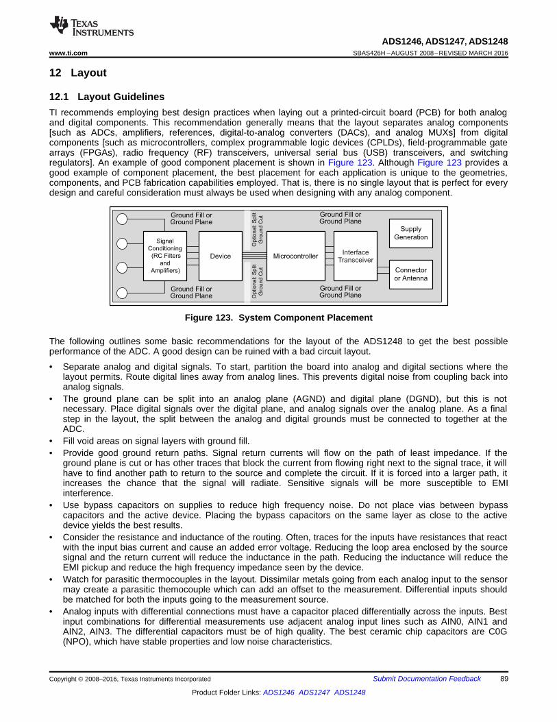
Device Microcontroller
Signal
Conditioning
(RC Filters
and
Amplifiers)
Supply
Generation
Connector
or Antenna
Ground Fill orGround Plane
Optional: S
plit
Gro
und
CutGround Fill or
Ground Plane
Optional: S
plit
Gro
und C
ut
InterfaceTransceiver
Ground Fill orGround Plane
Ground Fill orGround Plane
89
ADS1246, ADS1247, ADS1248www.ti.com SBAS426H –AUGUST 2008–REVISED MARCH 2016
Product Folder Links: ADS1246 ADS1247 ADS1248
Submit Documentation FeedbackCopyright © 2008–2016, Texas Instruments Incorporated
12 Layout
12.1 Layout GuidelinesTI recommends employing best design practices when laying out a printed-circuit board (PCB) for both analogand digital components. This recommendation generally means that the layout separates analog components[such as ADCs, amplifiers, references, digital-to-analog converters (DACs), and analog MUXs] from digitalcomponents [such as microcontrollers, complex programmable logic devices (CPLDs), field-programmable gatearrays (FPGAs), radio frequency (RF) transceivers, universal serial bus (USB) transceivers, and switchingregulators]. An example of good component placement is shown in Figure 123. Although Figure 123 provides agood example of component placement, the best placement for each application is unique to the geometries,components, and PCB fabrication capabilities employed. That is, there is no single layout that is perfect for everydesign and careful consideration must always be used when designing with any analog component.
Figure 123. System Component Placement
The following outlines some basic recommendations for the layout of the ADS1248 to get the best possibleperformance of the ADC. A good design can be ruined with a bad circuit layout.
• Separate analog and digital signals. To start, partition the board into analog and digital sections where thelayout permits. Route digital lines away from analog lines. This prevents digital noise from coupling back intoanalog signals.
• The ground plane can be split into an analog plane (AGND) and digital plane (DGND), but this is notnecessary. Place digital signals over the digital plane, and analog signals over the analog plane. As a finalstep in the layout, the split between the analog and digital grounds must be connected to together at theADC.
• Fill void areas on signal layers with ground fill.• Provide good ground return paths. Signal return currents will flow on the path of least impedance. If the
ground plane is cut or has other traces that block the current from flowing right next to the signal trace, it willhave to find another path to return to the source and complete the circuit. If it is forced into a larger path, itincreases the chance that the signal will radiate. Sensitive signals will be more susceptible to EMIinterference.
• Use bypass capacitors on supplies to reduce high frequency noise. Do not place vias between bypasscapacitors and the active device. Placing the bypass capacitors on the same layer as close to the activedevice yields the best results.
• Consider the resistance and inductance of the routing. Often, traces for the inputs have resistances that reactwith the input bias current and cause an added error voltage. Reducing the loop area enclosed by the sourcesignal and the return current will reduce the inductance in the path. Reducing the inductance will reduce theEMI pickup and reduce the high frequency impedance seen by the device.
• Watch for parasitic thermocouples in the layout. Dissimilar metals going from each analog input to the sensormay create a parasitic themocouple which can add an offset to the measurement. Differential inputs shouldbe matched for both the inputs going to the measurement source.
• Analog inputs with differential connections must have a capacitor placed differentially across the inputs. Bestinput combinations for differential measurements use adjacent analog input lines such as AIN0, AIN1 andAIN2, AIN3. The differential capacitors must be of high quality. The best ceramic chip capacitors are C0G(NPO), which have stable properties and low noise characteristics.
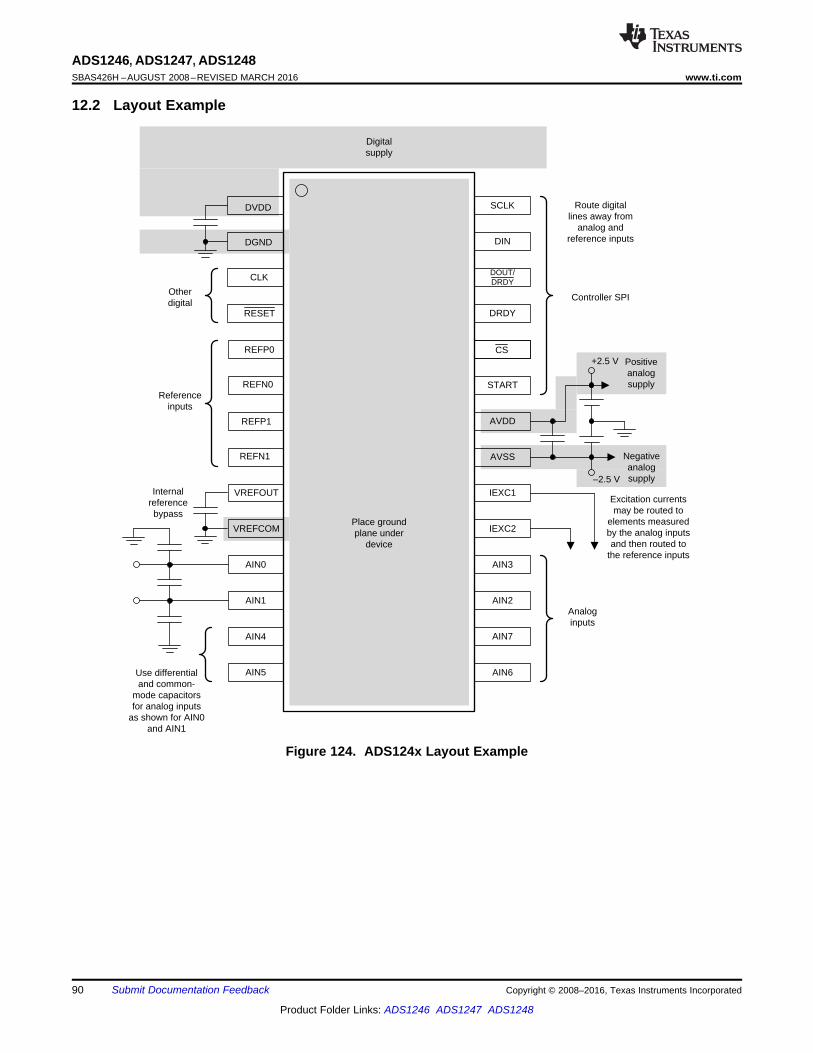
AVDD
IEXC1
DVDD
DGND
AIN6
AIN7
VREFOUT
AIN4
AIN5
+2.5 V
±2.5 V
AIN0
AIN1
START
AVSS
IEXC2
AIN3
AIN2
Positive analog supply
Negative analog supply
Digital supply
Place groundplane under
device
Route digital lines away from
analog and reference inputs
DRDY
SCLK
DIN
DOUT/DRDYCLK
RESET
REFP0
REFN0
REFP1
REFN1
VREFCOM
CS
Controller SPI
Use differential and common-
mode capacitors for analog inputs
as shown for AIN0 and AIN1
Other digital
Analog inputs
Excitation currents may be routed to
elements measured by the analog inputs and then routed to
the reference inputs
Reference inputs
Internal reference bypass
90
ADS1246, ADS1247, ADS1248SBAS426H –AUGUST 2008–REVISED MARCH 2016 www.ti.com
Product Folder Links: ADS1246 ADS1247 ADS1248
Submit Documentation Feedback Copyright © 2008–2016, Texas Instruments Incorporated
12.2 Layout Example
Figure 124. ADS124x Layout Example

91
ADS1246, ADS1247, ADS1248www.ti.com SBAS426H –AUGUST 2008–REVISED MARCH 2016
Product Folder Links: ADS1246 ADS1247 ADS1248
Submit Documentation FeedbackCopyright © 2008–2016, Texas Instruments Incorporated
13 Device and Documentation Support
13.1 Documentation Support
13.1.1 Related DocumentationFor related documentation see the following:• Example Temperature Measurement Applications Using the ADS1247 and ADS1248, SBAA180• RTD Ratiometric Measurements and Filtering Using the ADS1148 and ADS1248 Family of Devices,
SBAA201• 3-Wire RTD Measurement System Reference Design, –200°C to 850°C, SLAU520• A Glossary of Analog-to-Digital Specifications and Performance Characteristics, SBAA147
13.2 Related LinksThe table below lists quick access links. Categories include technical documents, support and communityresources, tools and software, and quick access to sample or buy.
Table 54. Related Links
PARTS PRODUCT FOLDER SAMPLE & BUY TECHNICALDOCUMENTS
TOOLS &SOFTWARE
SUPPORT &COMMUNITY
ADS1246 Click here Click here Click here Click here Click hereADS1247 Click here Click here Click here Click here Click hereADS1248 Click here Click here Click here Click here Click here
13.3 Community ResourcesThe following links connect to TI community resources. Linked contents are provided "AS IS" by the respectivecontributors. They do not constitute TI specifications and do not necessarily reflect TI's views; see TI's Terms ofUse.
TI E2E™ Online Community TI's Engineer-to-Engineer (E2E) Community. Created to foster collaborationamong engineers. At e2e.ti.com, you can ask questions, share knowledge, explore ideas and helpsolve problems with fellow engineers.
Design Support TI's Design Support Quickly find helpful E2E forums along with design support tools andcontact information for technical support.
13.4 TrademarksE2E is a trademark of Texas Instruments.SPI is a trademark of Motorola, Inc.All other trademarks are the property of their respective owners.
13.5 Electrostatic Discharge CautionThis integrated circuit can be damaged by ESD. Texas Instruments recommends that all integrated circuits be handled withappropriate precautions. Failure to observe proper handling and installation procedures can cause damage.
ESD damage can range from subtle performance degradation to complete device failure. Precision integrated circuits may be moresusceptible to damage because very small parametric changes could cause the device not to meet its published specifications.
13.6 GlossarySLYZ022 — TI Glossary.
This glossary lists and explains terms, acronyms, and definitions.
14 Mechanical, Packaging, and Orderable InformationThe following pages include mechanical, packaging, and orderable information. This information is the mostcurrent data available for the designated devices. This data is subject to change without notice and revision ofthis document. For browser-based versions of this data sheet, refer to the left-hand navigation.

PACKAGE OPTION ADDENDUM
www.ti.com 25-Oct-2014
Addendum-Page 1
PACKAGING INFORMATION
Orderable Device Status(1)
Package Type PackageDrawing
Pins PackageQty
Eco Plan(2)
Lead/Ball Finish(6)
MSL Peak Temp(3)
Op Temp (°C) Device Marking(4/5)
Samples
ADS1246IPW ACTIVE TSSOP PW 16 90 Green (RoHS& no Sb/Br)
CU NIPDAU Level-1-260C-UNLIM -40 to 105 ADS1246
ADS1246IPWR ACTIVE TSSOP PW 16 2000 Green (RoHS& no Sb/Br)
CU NIPDAU Level-1-260C-UNLIM -40 to 105 ADS1246
ADS1247IPW ACTIVE TSSOP PW 20 70 Green (RoHS& no Sb/Br)
CU NIPDAU Level-2-260C-1 YEAR -40 to 105 ADS1247
ADS1247IPWR ACTIVE TSSOP PW 20 2000 Green (RoHS& no Sb/Br)
CU NIPDAU Level-2-260C-1 YEAR -40 to 105 ADS1247
ADS1248IPW ACTIVE TSSOP PW 28 50 Green (RoHS& no Sb/Br)
CU NIPDAU Level-2-260C-1 YEAR -40 to 105 ADS1248
ADS1248IPWR ACTIVE TSSOP PW 28 2000 Green (RoHS& no Sb/Br)
CU NIPDAU Level-2-260C-1 YEAR -40 to 105 ADS1248
(1) The marketing status values are defined as follows:ACTIVE: Product device recommended for new designs.LIFEBUY: TI has announced that the device will be discontinued, and a lifetime-buy period is in effect.NRND: Not recommended for new designs. Device is in production to support existing customers, but TI does not recommend using this part in a new design.PREVIEW: Device has been announced but is not in production. Samples may or may not be available.OBSOLETE: TI has discontinued the production of the device.
(2) Eco Plan - The planned eco-friendly classification: Pb-Free (RoHS), Pb-Free (RoHS Exempt), or Green (RoHS & no Sb/Br) - please check http://www.ti.com/productcontent for the latest availabilityinformation and additional product content details.TBD: The Pb-Free/Green conversion plan has not been defined.Pb-Free (RoHS): TI's terms "Lead-Free" or "Pb-Free" mean semiconductor products that are compatible with the current RoHS requirements for all 6 substances, including the requirement thatlead not exceed 0.1% by weight in homogeneous materials. Where designed to be soldered at high temperatures, TI Pb-Free products are suitable for use in specified lead-free processes.Pb-Free (RoHS Exempt): This component has a RoHS exemption for either 1) lead-based flip-chip solder bumps used between the die and package, or 2) lead-based die adhesive used betweenthe die and leadframe. The component is otherwise considered Pb-Free (RoHS compatible) as defined above.Green (RoHS & no Sb/Br): TI defines "Green" to mean Pb-Free (RoHS compatible), and free of Bromine (Br) and Antimony (Sb) based flame retardants (Br or Sb do not exceed 0.1% by weightin homogeneous material)
(3) MSL, Peak Temp. - The Moisture Sensitivity Level rating according to the JEDEC industry standard classifications, and peak solder temperature.
(4) There may be additional marking, which relates to the logo, the lot trace code information, or the environmental category on the device.
(5) Multiple Device Markings will be inside parentheses. Only one Device Marking contained in parentheses and separated by a "~" will appear on a device. If a line is indented then it is a continuationof the previous line and the two combined represent the entire Device Marking for that device.

PACKAGE OPTION ADDENDUM
www.ti.com 25-Oct-2014
Addendum-Page 2
(6) Lead/Ball Finish - Orderable Devices may have multiple material finish options. Finish options are separated by a vertical ruled line. Lead/Ball Finish values may wrap to two lines if the finishvalue exceeds the maximum column width.
Important Information and Disclaimer:The information provided on this page represents TI's knowledge and belief as of the date that it is provided. TI bases its knowledge and belief on informationprovided by third parties, and makes no representation or warranty as to the accuracy of such information. Efforts are underway to better integrate information from third parties. TI has taken andcontinues to take reasonable steps to provide representative and accurate information but may not have conducted destructive testing or chemical analysis on incoming materials and chemicals.TI and TI suppliers consider certain information to be proprietary, and thus CAS numbers and other limited information may not be available for release.
In no event shall TI's liability arising out of such information exceed the total purchase price of the TI part(s) at issue in this document sold by TI to Customer on an annual basis.

TAPE AND REEL INFORMATION
*All dimensions are nominal
Device PackageType
PackageDrawing
Pins SPQ ReelDiameter
(mm)
ReelWidth
W1 (mm)
A0(mm)
B0(mm)
K0(mm)
P1(mm)
W(mm)
Pin1Quadrant
ADS1246IPWR TSSOP PW 16 2000 330.0 12.4 6.9 5.6 1.6 8.0 12.0 Q1
ADS1247IPWR TSSOP PW 20 2000 330.0 16.4 6.95 7.1 1.6 8.0 16.0 Q1
ADS1248IPWR TSSOP PW 28 2000 330.0 16.4 6.9 10.2 1.8 12.0 16.0 Q1
PACKAGE MATERIALS INFORMATION
www.ti.com 25-Oct-2014
Pack Materials-Page 1

*All dimensions are nominal
Device Package Type Package Drawing Pins SPQ Length (mm) Width (mm) Height (mm)
ADS1246IPWR TSSOP PW 16 2000 367.0 367.0 35.0
ADS1247IPWR TSSOP PW 20 2000 367.0 367.0 38.0
ADS1248IPWR TSSOP PW 28 2000 367.0 367.0 38.0
PACKAGE MATERIALS INFORMATION
www.ti.com 25-Oct-2014
Pack Materials-Page 2


IMPORTANT NOTICE
Texas Instruments Incorporated and its subsidiaries (TI) reserve the right to make corrections, enhancements, improvements and otherchanges to its semiconductor products and services per JESD46, latest issue, and to discontinue any product or service per JESD48, latestissue. Buyers should obtain the latest relevant information before placing orders and should verify that such information is current andcomplete. All semiconductor products (also referred to herein as “components”) are sold subject to TI’s terms and conditions of salesupplied at the time of order acknowledgment.TI warrants performance of its components to the specifications applicable at the time of sale, in accordance with the warranty in TI’s termsand conditions of sale of semiconductor products. Testing and other quality control techniques are used to the extent TI deems necessaryto support this warranty. Except where mandated by applicable law, testing of all parameters of each component is not necessarilyperformed.TI assumes no liability for applications assistance or the design of Buyers’ products. Buyers are responsible for their products andapplications using TI components. To minimize the risks associated with Buyers’ products and applications, Buyers should provideadequate design and operating safeguards.TI does not warrant or represent that any license, either express or implied, is granted under any patent right, copyright, mask work right, orother intellectual property right relating to any combination, machine, or process in which TI components or services are used. Informationpublished by TI regarding third-party products or services does not constitute a license to use such products or services or a warranty orendorsement thereof. Use of such information may require a license from a third party under the patents or other intellectual property of thethird party, or a license from TI under the patents or other intellectual property of TI.Reproduction of significant portions of TI information in TI data books or data sheets is permissible only if reproduction is without alterationand is accompanied by all associated warranties, conditions, limitations, and notices. TI is not responsible or liable for such altereddocumentation. Information of third parties may be subject to additional restrictions.Resale of TI components or services with statements different from or beyond the parameters stated by TI for that component or servicevoids all express and any implied warranties for the associated TI component or service and is an unfair and deceptive business practice.TI is not responsible or liable for any such statements.Buyer acknowledges and agrees that it is solely responsible for compliance with all legal, regulatory and safety-related requirementsconcerning its products, and any use of TI components in its applications, notwithstanding any applications-related information or supportthat may be provided by TI. Buyer represents and agrees that it has all the necessary expertise to create and implement safeguards whichanticipate dangerous consequences of failures, monitor failures and their consequences, lessen the likelihood of failures that might causeharm and take appropriate remedial actions. Buyer will fully indemnify TI and its representatives against any damages arising out of the useof any TI components in safety-critical applications.In some cases, TI components may be promoted specifically to facilitate safety-related applications. With such components, TI’s goal is tohelp enable customers to design and create their own end-product solutions that meet applicable functional safety standards andrequirements. Nonetheless, such components are subject to these terms.No TI components are authorized for use in FDA Class III (or similar life-critical medical equipment) unless authorized officers of the partieshave executed a special agreement specifically governing such use.Only those TI components which TI has specifically designated as military grade or “enhanced plastic” are designed and intended for use inmilitary/aerospace applications or environments. Buyer acknowledges and agrees that any military or aerospace use of TI componentswhich have not been so designated is solely at the Buyer's risk, and that Buyer is solely responsible for compliance with all legal andregulatory requirements in connection with such use.TI has specifically designated certain components as meeting ISO/TS16949 requirements, mainly for automotive use. In any case of use ofnon-designated products, TI will not be responsible for any failure to meet ISO/TS16949.
Products ApplicationsAudio www.ti.com/audio Automotive and Transportation www.ti.com/automotiveAmplifiers amplifier.ti.com Communications and Telecom www.ti.com/communicationsData Converters dataconverter.ti.com Computers and Peripherals www.ti.com/computersDLP® Products www.dlp.com Consumer Electronics www.ti.com/consumer-appsDSP dsp.ti.com Energy and Lighting www.ti.com/energyClocks and Timers www.ti.com/clocks Industrial www.ti.com/industrialInterface interface.ti.com Medical www.ti.com/medicalLogic logic.ti.com Security www.ti.com/securityPower Mgmt power.ti.com Space, Avionics and Defense www.ti.com/space-avionics-defenseMicrocontrollers microcontroller.ti.com Video and Imaging www.ti.com/videoRFID www.ti-rfid.comOMAP Applications Processors www.ti.com/omap TI E2E Community e2e.ti.comWireless Connectivity www.ti.com/wirelessconnectivity
Mailing Address: Texas Instruments, Post Office Box 655303, Dallas, Texas 75265Copyright © 2016, Texas Instruments Incorporated