advance 4gb d-die nand flashguimli.free.fr/download/k9f4g.pdf · the cle input controls the...
TRANSCRIPT

- 1 -
Rev.0.2, May. 2010
SAMSUNG ELECTRONICS RESERVES THE RIGHT TO CHANGE PRODUCTS, INFORMATION AND SPECIFICATIONS WITHOUT NOTICE.
Products and specifications discussed herein are for reference purposes only. All information discussed herein is provided on an "AS IS" basis, without warranties of any kind.
This document and all information discussed herein remain the sole and exclusive property of Samsung Electronics. No license of any patent, copyright, mask work, trademark or any other intellectual property right is granted by one party to the other party under this document, by implication, estoppel or other-wise.
Samsung products are not intended for use in life support, critical care, medical, safety equipment, or similar applications where product failure could result in loss of life or personal or physical harm, or any military or defense application, or any governmental procurement to which special terms or provisions may apply.
For updates or additional information about Samsung products, contact your nearest Samsung office.
All brand names, trademarks and registered trademarks belong to their respective owners.
ⓒ 2010 Samsung Electronics Co., Ltd. All rights reserved.
K9F4G08U0DK9K8G08U0DK9K8G08U1DK9WAG08U1D
Advance
4Gb D-die NAND FlashSingle-Level-Cell (1bit/cell)
datasheet

- 2 -
datasheetK9K8G08U0D FLASH MEMORYRev. 0.2Advance
K9F4G08U0D K9K8G08U1DK9WAG08U1D
Revision History
The attached data sheets are prepared and approved by SAMSUNG Electronics. SAMSUNG Electronics CO., LTD. reserve the right to change the specifications. SAMSUNG Electronics will evaluate and reply to your requests and questions about device. If you have any questions, please contact the SAMSUNG branch office near your office.
Revision No. History Draft Date Remark Editor
0.0 1. Initial issue Jan. 12, 2010 Advance -
0.1 1. Corrected errata.2. Chapter 1.2 Features revised.
May. 03, 2010 Advance H.K.Kim
0.2 1. DDP/QDP Part ID are added. May. 26, 2010 Advance H.K.Kim

- 3 -
Table Of Contents
datasheetK9K8G08U0D FLASH MEMORYRev. 0.2Advance
K9F4G08U0D K9K8G08U1DK9WAG08U1D
1.0 INTRODUCTION ........................................................................................................................................................ 41.1 General Description................................................................................................................................................. 41.2 Features .................................................................................................................................................................. 41.3 PRODUCT LIST ...................................................................................................................................................... 41.4 Pin Configuration (TSOP1)...................................................................................................................................... 5
1.4.1 PACKAGE DIMENSIONS ................................................................................................................................. 51.5 Pin Configuration (TSOP1)...................................................................................................................................... 6
1.5.1 PACKAGE DIMENSIONS ................................................................................................................................. 61.6 Pin Description ........................................................................................................................................................ 7
2.0 PRODUCT INTRODUCTION......................................................................................................................................92.1 Absolute Maximum Ratings..................................................................................................................................... 102.2 Recommended Operating Conditions ..................................................................................................................... 102.3 DC AND OPERATING CHARACTERISTICS(Recommended operating conditions otherwise noted.) ..................102.4 Valid Block............................................................................................................................................................... 112.5 Ac Test Condition .................................................................................................................................................... 112.6 Capacitance(TA=25°C, VCC=3.3V, f=1.0MHz) ....................................................................................................... 112.7 Mode Selection........................................................................................................................................................ 112.8 Program / Erase Characteristics ........................................................................................................................122.9 AC Timing Characteristics for Command / Address / Data Input ............................................................................ 122.10 AC Characteristics for Operation........................................................................................................................... 13
3.0 NAND Flash Technical Notes .................................................................................................................................... 143.1 Initial Invalid Block(s) ............................................................................................................................................... 143.2 Identifying Initial Invalid Block(s) ............................................................................................................................. 143.3 Error in write or read operation................................................................................................................................ 153.4 Addressing for program operation ........................................................................................................................... 173.5 System Interface Using CE don’t-care. ................................................................................................................... 18
4.0 TIMING DIAGRAMS .................................................................................................................................................. 194.1 Command Latch Cycle ........................................................................................................................................... 194.2 Address Latch Cycle............................................................................................................................................... 194.3 Input Data Latch Cycle ........................................................................................................................................... 204.4 * Serial Access Cycle after Read(CLE=L, WE=H, ALE=L)..................................................................................... 204.5 Serial Access Cycle after Read(EDO Type, CLE=L, WE=H, ALE=L) .................................................................... 214.6 Status Read Cycle.................................................................................................................................................. 214.7 Read Operation ...................................................................................................................................................... 224.8 Read Operation(Intercepted by CE) ....................................................................................................................... 224.9 Random Data Output In a Page ............................................................................................................................. 234.10 Page Program Operation...................................................................................................................................... 244.11 Page Program Operation with Random Data Input .............................................................................................. 254.12 Copy-Back Program Operation ............................................................................................................................ 264.13 Copy-Back Program Operation with Random Data Input ..................................................................................... 274.14 Two-Plane Page Program Operation ................................................................................................................... 284.15 Block Erase Operation.......................................................................................................................................... 294.16 Two-Plane Block Erase Operation ....................................................................................................................... 304.17 Read ID Operation................................................................................................................................................ 31
5.0 DEVICE OPERATION ................................................................................................................................................ 335.1 Page Read............................................................................................................................................................... 335.2 Page Program ......................................................................................................................................................... 345.3 Copy-back Program................................................................................................................................................. 355.4 Block Erase ............................................................................................................................................................. 365.5 Two-plane Page Program........................................................................................................................................ 365.6 Two-plane Block Erase............................................................................................................................................ 375.7 Two-plane Copy-back Program............................................................................................................................... 375.8 Read Status............................................................................................................................................................. 395.9 Read ID ................................................................................................................................................................... 405.10 Reset ..................................................................................................................................................................... 405.11 Ready/Busy ........................................................................................................................................................... 415.12 Data Protection & Power Up Sequence ................................................................................................................ 42

- 4 -
datasheetK9K8G08U0D FLASH MEMORYRev. 0.2Advance
K9F4G08U0D K9K8G08U1DK9WAG08U1D
1.0 INTRODUCTION
1.1 General Description
Offered in 512Mx8bit, the K9F4G08U0D is a 4G-bit NAND Flash Memory with spare 128M-bit. The device is offered in 3.3V Vcc. Its NAND cell provides the most cost-effective solution for the solid state application market. A program operation can be performed in typical 250μs on the (2K+64)Byte page and an erase operation can be performed in typical 2ms on a (128K+4K)Byte block. Data in the data register can be read out at 25ns cycle time per Byte. The I/O pins serve as the ports for address and data input/output as well as command input. The on-chip write controller automates all program and erase functions including pulse repetition, where required, and internal verification and margining of data. Even the write-intensive systems can take advantage of the K9F4G08U0D′s extended reliability of 100K program/erase cycles by providing ECC(Error Correcting Code) with real time mapping-out algorithm. The K9F4G08U0D is an optimum solution for large nonvolatile storage applications such as solid state file storage and other portable applications requir-ing non-volatility.
1.2 Features
1.3 PRODUCT LIST
• Voltage Supply - 3.3V Device(K9F4G08U0D) : 2.7V ~ 3.6V• Organization - Memory Cell Array : (512M + 16M) x 8bit - Data Register : (2K + 64) x 8bit • Automatic Program and Erase - Page Program : (2K + 64)Byte - Block Erase : (128K + 4K)Byte• Page Read Operation - Page Size : (2K + 64)Byte - Random Read : 25μs(Max.) - Serial Access : 25ns(Min.) • Fast Write Cycle Time - Page Program time : 250μs(Typ.) - Block Erase Time : 2ms(Typ.)
• Command/Address/Data Multiplexed I/O Port• Hardware Data Protection - Program/Erase Lockout During Power Transitions• Reliable CMOS Floating-Gate Technology - ECC Requirement : 1bit/528Byte - Endurance & Data Retention : Please refer to the qualification report• Command Register Operation• Unique ID for Copyright Protection• Package : - K9F4G08U0D-SCB0/SIB0 : Pb-FREE, Halogen-FREE PACKAGE 48 - Pin TSOP1 (12 x 20 / 0.5 mm pitch) - K9K8G08U0D-SCB0/SIB0 : Pb-FREE, Halogen-FREE PACKAGE 48 - Pin TSOP1 (12 x 20 / 0.5 mm pitch) - K9K8G08U1D-SCB0/SIB0 : Pb-FREE, Halogen-FREE PACKAGE 48 - Pin TSOP1 (12 x 20 / 0.5 mm pitch) - K9WAG08U1D-SCB0/SIB0 : Pb-FREE, Halogen-FREE PACKAGE 48 - Pin TSOP1 (12 x 20 / 0.5 mm pitch)
Part Number Vcc Range Organization PKG Type
K9F4G08U0D-S
2.70 ~ 3.60V X8 TSOP1K9K8G08U0D-S
K9K8G08U1D-S
K9WAG08U1D-S

- 5 -
datasheetK9K8G08U0D FLASH MEMORYRev. 0.2Advance
K9F4G08U0D K9K8G08U1DK9WAG08U1D
1.4 Pin Configuration (TSOP1)
1.4.1 PACKAGE DIMENSIONS
K9F4G08U0D-SCB0/SIB0K9K8G08U0D-SCB0/SIB0
48-pin TSOP1Standard Type12mm x 20mm
123456789101112131415161718192021222324
484746454443424140393837363534333231302928272625
N.CN.CN.CN.CN.C
R/B1 RE
CE1N.CN.CVccVssN.CN.CCLEALEWEWPN.CN.CN.CN.CN.C
N.CN.CN.CN.CI/O7I/O6I/O5I/O4N.CN.CN.CVccVssN.CN.CN.CI/O3I/O2I/O1I/O0N.CN.CN.CN.C
N.C
48-PIN LEAD FREE PLASTIC THIN SMALL OUT-LINE PACKAGE TYPE(I)48 - TSOP1 - 1220F Unit :mm/Inch
0.787±0.00820.00±0.20
#1
#24
0.20
+0.0
7-0
.03
0.00
8+0.0
03-0
.001
0.50
0.01
97
#48
#25
0.48
812
.40
MA
X
12.0
00.
472
0.10
0.
004
MA
X
0.25
0.01
0(
)
0.039±0.0021.00±0.05
0.0020.05 MIN
0.0471.20 MAX
0.45~0.750.018~0.030
0.724±0.00418.40±0.10
0~8°
0.01
00.
25TY
P
0.12
5+0
.075
0.03
5
0.00
5+0.0
03-0
.001
0.500.020( )

- 6 -
datasheetK9K8G08U0D FLASH MEMORYRev. 0.2Advance
K9F4G08U0D K9K8G08U1DK9WAG08U1D
1.5 Pin Configuration (TSOP1)
1.5.1 PACKAGE DIMENSIONS
48-pin TSOP1Standard Type12mm x 20mm
123456789101112131415161718192021222324
484746454443424140393837363534333231302928272625
N.CN.CN.CN.CN.C
R/B1 RE
CE1CE2N.CVccVssN.CN.CCLEALEWEWPN.CN.CN.CN.CN.C
N.CN.CN.CN.CI/O7I/O6I/O5I/O4N.CN.CN.CVccVssN.CN.CN.CI/O3I/O2I/O1I/O0N.CN.CN.CN.C
K9WAG08U1D-SCB0/SIB0
R/B2
K9K8G08U1D-SCB0/SIB0
48-PIN LEAD FREE PLASTIC THIN SMALL OUT-LINE PACKAGE TYPE(I)48 - TSOP1 - 1220F Unit :mm/Inch
0.787±0.00820.00±0.20
#1
#24
0.20
+0.0
7-0
.03
0.00
8+0.0
03-0
.001
0.50
0.01
97
#48
#25
0.48
812
.40
MA
X
12.0
00.
472
0.10
0.
004
MA
X
0.25
0.01
0(
)
0.039±0.0021.00±0.05
0.0020.05 MIN
0.0471.20 MAX
0.45~0.750.018~0.030
0.724±0.00418.40±0.10
0~8°
0.01
00.
25TY
P
0.12
5+0
.075
0.03
5
0.00
5+0.0
03-0
.001
0.500.020( )

- 7 -
datasheetK9K8G08U0D FLASH MEMORYRev. 0.2Advance
K9F4G08U0D K9K8G08U1DK9WAG08U1D
1.6 Pin Description
NOTE : Connect all VCC and VSS pins of each device to common power supply outputs.Do not leave VCC or VSS disconnected.
Pin Name Pin Function
I/O0 ~ I/O7DATA INPUTS/OUTPUTS The I/O pins are used to input command, address and data, and to output data during read operations. The I/O pins float to high-z when the chip is deselected or when the outputs are disabled.
CLECOMMAND LATCH ENABLEThe CLE input controls the activating path for commands sent to the command register. When active high, commands are latched into the command register through the I/O ports on the rising edge of the WE signal.
ALEADDRESS LATCH ENABLEThe ALE input controls the activating path for address to the internal address registers. Addresses are latched on the rising edge of WE with ALE high.
CECHIP ENABLEThe CE input is the device selection control. When the device is in the Busy state, CE high is ignored, and the device does not return to standby mode in program or erase operation.
REREAD ENABLEThe RE input is the serial data-out control, and when active drives the data onto the I/O bus. Data is valid tREA after the fall-ing edge of RE which also increments the internal column address counter by one.
WE WRITE ENABLEThe WE input controls writes to the I/O port. Commands, address and data are latched on the rising edge of the WE pulse.
WPWRITE PROTECTThe WP pin provides inadvertent program/erase protection during power transitions. The internal high voltage generator is reset when the WP pin is active low.
R/B
READY/BUSY OUTPUTThe R/B output indicates the status of the device operation. When low, it indicates that a program, erase or random read oper-ation is in process and returns to high state upon completion. It is an open drain output and does not float to high-z condition when the chip is deselected or when outputs are disabled.
Vcc POWERVCC is the power supply for device.
Vss GROUND
N.C NO CONNECTIONLead is not internally connected.

[Figure 2] K9F4G08U0D Array Organization
[Figure 1] K9F4G08U0D Functional Block Diagram
- 8 -
datasheetK9K8G08U0D FLASH MEMORYRev. 0.2Advance
K9F4G08U0D K9K8G08U1DK9WAG08U1D
NOTE : Column Address : Starting Address of the Register.* L must be set to "Low".* The device ignores any additional input of address cycles than required.
I/O 0 I/O 1 I/O 2 I/O 3 I/O 4 I/O 5 I/O 6 I/O 7
1st Cycle A0 A1 A2 A3 A4 A5 A6 A7
2nd Cycle A8 A9 A10 A11 *L *L *L *L
3rd Cycle A12 A13 A14 A15 A16 A17 A18 A19
4th Cycle A20 A21 A22 A23 A24 A25 A26 A27
5th Cycle A28 A29 *L *L *L *L *L *L
VCC
X-Buffers
Command
I/O Buffers & Latches
Latches& Decoders
Y-BuffersLatches& Decoders
Register
Control Logic& High Voltage
Generator Global Buffers OutputDriver
VSS
A12 - A29
A0 - A11
Command
CEREWE
CLE WP
I/0 0
I/0 7
VCCVSS
ALE
4,096M + 128M BitNAND Flash
ARRAY
(2,048 + 64)Byte x 262,144
Y-Gating
Data Register & S/A
2K Bytes 64 Bytes
256K Pages(=4,096 Blocks)
2K Bytes
8 bit
64 Bytes
1 Block = 64 Pages(128K + 4K) Byte
I/O 0 ~ I/O 7
1 Page = (2K + 64)Bytes1 Block = (2K + 64)B x 64 Pages = (128K + 4K) Bytes1 Device = (2K+64)B x 64Pages x 4,096 Blocks = 4,224 Mbits
Page Register
Column Address
Row Address : Page Address : A12 ~ A17 Plane Address : A18
Block Address : A19 ~ the last Address
- 9 -
datasheetK9K8G08U0D FLASH MEMORYRev. 0.2Advance
K9F4G08U0D K9K8G08U1DK9WAG08U1D
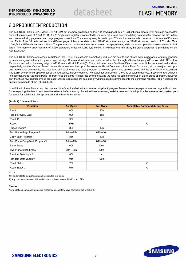
2.0 PRODUCT INTRODUCTIONThe K9F4G08U0D is a 4,224Mbit(4,429,185,024 bit) memory organized as 262,144 rows(pages) by 2,112x8 columns. Spare 64x8 columns are located from column address of 2,048~2,111. A 2,112-byte data register is connected to memory cell arrays accommodating data transfer between the I/O buffers and memory during page read and page program operations. The memory array is made up of 32 cells that are serially connected to form a NAND struc-ture. Each of the 32 cells resides in a different page. A block consists of two NAND structured strings. A NAND structure consists of 32 cells. Total 1,081,344 NAND cells reside in a block. The program and read operations are executed on a page basis, while the erase operation is executed on a block basis. The memory array consists of 4,096 separately erasable 128K-byte blocks. It indicates that the bit by bit erase operation is prohibited on the K9F4G08U0D.
The K9F4G08U0D has addresses multiplexed into 8 I/Os. This scheme dramatically reduces pin counts and allows system upgrades to future densities by maintaining consistency in system board design. Command, address and data are all written through I/O's by bringing WE to low while CE is low. Those are latched on the rising edge of WE. Command Latch Enable(CLE) and Address Latch Enable(ALE) are used to multiplex command and address respectively, via the I/O pins. Some commands require one bus cycle. For example, Reset Command, Status Read Command, etc require just one cycle bus. Some other commands, like page read and block erase and page program, require two cycles: one cycle for setup and the other cycle for execution. The 528M byte physical space requires 30 addresses, thereby requiring five cycles for addressing : 2 cycles of column address, 3 cycles of row address, in that order. Page Read and Page Program need the same five address cycles following the required command input. In Block Erase operation, however, only the three row address cycles are used. Device operations are selected by writing specific commands into the command register. Table 1 defines the specific commands of the K9F4G08U0D.
In addition to the enhanced architecture and interface, the device incorporates copy-back program feature from one page to another page without need for transporting the data to and from the external buffer memory. Since the time-consuming serial access and data-input cycles are removed, system per-formance for solid-state disk application is significantly increased.
[Table 1] Command Sets
NOTE :1) Random Data Input/Output can be executed in a page.2) Any command between 11h and 81h is prohibited except 70h/F1h and FFh.
Caution : Any undefined command inputs are prohibited except for above command set of Table 1.
Function 1st Cycle 2nd Cycle Acceptable Command during Busy
Read 00h 30h
Read for Copy Back 00h 35h
Read ID 90h -
Reset FFh - O
Page Program 80h 10h
Two-Plane Page Program(2) 80h---11h 81h---10h
Copy-Back Program 85h 10h
Two-Plane Copy-Back Program(2) 85h---11h 81h---10h
Block Erase 60h D0h
Two-Plane Block Erase 60h---60h D0h
Random Data Input(1) 85h -
Random Data Output(1) 05h E0h
Read Status 70h O
Read Status 2 F1h O

- 10 -
datasheetK9K8G08U0D FLASH MEMORYRev. 0.2Advance
K9F4G08U0D K9K8G08U1DK9WAG08U1D
2.1 Absolute Maximum Ratings
NOTE : 1) Minimum DC voltage is -0.6V on input/output pins. During transitions, this level may undershoot to -2.0V for periods <30ns. Maximum DC voltage on input/output pins is VCC+0.3V which, during transitions, may overshoot to VCC+2.0V for periods <20ns.2) Permanent device damage may occur if ABSOLUTE MAXIMUM RATINGS are exceeded. Functional operation should be restricted to the conditions as detailed in the operational sections of this data sheet. Exposure to absolute maximum rating conditions for extended periods may affect reliability.
2.2 Recommended Operating Conditions(Voltage reference to GND, K9XXG08XXD-XCB0 :TA=0 to 70°C, K9XXG08XXD-XIB0:TA=-40 to 85°C)
2.3 DC AND OPERATING CHARACTERISTICS(Recommended operating conditions otherwise noted.)
NOTE :1) VIL can undershoot to -0.4V and VIH can overshoot to VCC + 0.4V for durations of 20 ns or less.2) Typical value is measured at Vcc=/3.3V, TA=25°C. Not 100% tested.3) The typical value of the K9K8G08U1D's ISB2 is 20μA and the maximum value is 100μA. 4) The typical value of the K9K8G08U0D's ISB2 is 20μA and the maximum value is 100μA.5) The typical value of the K9WAG08U1D's ISB2 is 40μA and the maximum value is 200μA.
Parameter Symbol Rating Unit
Voltage on any pin relative to VSS
VCC -0.6 to +4.6
VVIN -0.6 to +4.6
VI/O -0.6 to Vcc + 0.3 (< 4.6V)
Temperature Under BiasK9XXG08XXD-XCB0
TBIAS-10 to +125
°CK9XXG08XXD-XIB0 -40 to +125
Storage TemperatureK9XXG08XXD-XCB0
TSTG -65 to +150 °CK9XXG08XXD-XIB0
Short Circuit Current IOS 5 mA
Parameter SymbolK9F4G08U0D(3.3V)
UnitMin Typ. Max
Supply Voltage VCC 2.7 3.3 3.6 V
Supply Voltage VSS 0 0 0 V
Parameter Symbol Test Conditions3.3V
Min Typ Max Unit
Operating Current
Page Read with Serial Access ICC1 tRC=50ns, CE=VIL
IOUT=0mA - 15 30
mAProgram ICC2 - - 15 30
Erase ICC3 - - 15 30
Stand-by Current(TTL) ISB1 CE=VIH, WP=PRE=0V/VCC - - 1
Stand-by Current(CMOS) ISB2CE=VCC-0.2, WP=PRE=0V/VCC
- 10 50
μAInput Leakage Current ILI VIN=0 to Vcc(max) - - ±10
Output Leakage Current ILO VOUT=0 to Vcc(max) - - ±10
Input High Voltage VIH* - 2.0 -VCC
+0.3
VInput Low Voltage, All inputs VIL* - -0.3 - 0.8
Output High Voltage Level VOH K9F4G08U0D :IOH=-400μA 2.4 - -
Output Low Voltage Level VOL K9F4G08U0D :IOL=2.1mA - - 0.4
Output Low Current(R/B) IOL(R/B) K9F4G08U0D :VOL=0.4V 8 10 - mA

- 11 -
datasheetK9K8G08U0D FLASH MEMORYRev. 0.2Advance
K9F4G08U0D K9K8G08U1DK9WAG08U1D
2.4 Valid Block
NOTE : 1) The device may include initial invalid blocks when first shipped. Additional invalid blocks may develop while being used. The number of valid blocks is presented with both
cases of invalid blocks considered. Invalid blocks are defined as blocks that contain one or more bad bits. Do not erase or program factory-marked bad blocks. Refer to the attached technical notes for appropriate management of invalid blocks.
2) The 1st block, which is placed on 00h block address, is guaranteed to be a valid block up to 1K program/erase cycles with 1bit/528Byte ECC.3) The number of valid block is on the basis of single plane operations, and this may be decreased with two plane operations.
2.5 Ac Test Condition(K9XXG08UXD-XCB0 :TA=0 to 70°C, K9F4G08UXD-XIB0:TA=-40 to 85°C, K9XXG08UXD: Vcc=2.7V~3.6V unless otherwise noted)
2.6 Capacitance(TA=25°C, VCC=3.3V, f=1.0MHz)
NOTE :1) Capacitance is periodically sampled and not 100% tested.2) CI/O(W)* and CIN(W)* are tested at wafer level.
2.7 Mode Selection
NOTE : 1) X can be VIL or VIH.
2) WP should be biased to CMOS high or CMOS low for standby.
Parameter Symbol Min Typ. Max Unit
K9F4G08U0D
NVB
4,016
-
4,096
BlocksK9K8G08U0D
8,032 8,192K9K8G08U1D
K9WAG08U1D 16,064 16,384
Parameter K9XXG08UXD
Input Pulse Levels 0V to Vcc
Input Rise and Fall Times 5ns
Input and Output Timing Levels Vcc/2
Output Load 1 TTL GATE and CL=50pF
Item Symbol Test Condition Min Max Unit
Input/Output CapacitanceCI/O VIL=0V - 8 pF
CI/O(W)* VIL=0V - 5 pF
Input CapacitanceCIN VIN=0V - 8 pF
CIN(W)* VIN=0V - 5 pF
CLE ALE CE WE RE WP Mode
H L L H XRead Mode
Command Input
L H L H X Address Input(5clock)
H L L H HWrite Mode
Command Input
L H L H H Address Input(5clock)
L L L H H Data Input
L L L H X Data Output
X X X X H X During Read(Busy)
X X X X X H During Program(Busy)
X X X X X H During Erase(Busy)
X X(1) X X X L Write Protect
X X H X X 0V/VCC(2) Stand-by

- 12 -
datasheetK9K8G08U0D FLASH MEMORYRev. 0.2Advance
K9F4G08U0D K9K8G08U1DK9WAG08U1D
2.8 Program / Erase Characteristics
NOTE : 1) Typical value is measured at Vcc=3.3V, TA=25°C. Not 100% tested.2) Typical program time is defined as the time within which more than 50% of the whole pages are programmed at 3.3V Vcc and 25°C temperature.
2.9 AC Timing Characteristics for Command / Address / Data Input
NOTE : 1) The transition of the corresponding control pins must occur only once while WE is held low2) tADL is the time from the WE rising edge of final address cycle to the WE rising edge of first data cycle
Parameter Symbol Min Typ Max Unit
Program Time tPROG - 250 750 μs
Dummy Busy Time for Two-Plane Page Program tDBSY - 0.5 1 μs
Number of Partial Program Cycles Nop - - 4 cycles
Block Erase Time tBERS - 2.0 10 ms
Parameter Symbol Min Max Unit
CLE Setup Time tCLS(1) 12 - ns
CLE Hold Time tCLH 5 - ns
CE Setup Time tCS(1) 20 - ns
CE Hold Time tCH 5 - ns
WE Pulse Width tWP 12 - ns
ALE Setup Time tALS(1) 12 - ns
ALE Hold Time tALH 5 - ns
Data Setup Time tDS(1) 12 - ns
Data Hold Time tDH 5 - ns
Write Cycle Time tWC 25 - ns
WE High Hold Time tWH 10 - ns
Address to Data Loading Time tADL(2) 70 - ns

- 13 -
datasheetK9K8G08U0D FLASH MEMORYRev. 0.2Advance
K9F4G08U0D K9K8G08U1DK9WAG08U1D
2.10 AC Characteristics for Operation
NOTE : 1) If reset command(FFh) is written at Ready state, the device goes into Busy for maximum 5μs.
Parameter Symbol Min Max Unit
Data Transfer from Cell to Register tR - 25 μs
ALE to RE Delay tAR 10 - ns
CLE to RE Delay tCLR 10 - ns
Ready to RE Low tRR 20 - ns
RE Pulse Width tRP 12 - ns
WE High to Busy tWB - 100 ns
Read Cycle Time tRC 25 - ns
RE Access Time tREA - 20 ns
CE Access Time tCEA - 25 ns
RE High to Output Hi-Z tRHZ - 100 ns
CE High to Output Hi-Z tCHZ - 30 ns
RE High to Output Hold tRHOH 15 - ns
RE Low to Output Hold tRLOH 5 - ns
CE High to Output Hold tCOH 15 - ns
RE High Hold Time tREH 10 - ns
Output Hi-Z to RE Low tIR 0 - ns
RE High to WE Low tRHW 100 - ns
WE High to RE Low tWHR 60 - ns
Device Resetting Time(Read/Program/Erase) tRST - 5/10/500(1) μs

- 14 -
datasheetK9K8G08U0D FLASH MEMORYRev. 0.2Advance
K9F4G08U0D K9K8G08U1DK9WAG08U1D
3.0 NAND Flash Technical Notes
3.1 Initial Invalid Block(s)
[Figure 3] Flow chart to create initial invalid block table
Initial invalid blocks are defined as blocks that contain one or more initial invalid bits whose reliability is not guaranteed by Samsung. The information regarding the initial invalid block(s) is called the initial invalid block information. Devices with initial invalid block(s) have the same quality level as devices with all valid blocks and have the same AC and DC characteristics. An initial invalid block(s) does not affect the performance of valid block(s) because it is isolated from the bit line and the common source line by a select transistor. The system design must be able to mask out the initial invalid block(s) via address mapping. The 1st block, which is placed on 00h block address, is guaranteed to be a valid block up to 1K program/erase cycles with 1bit/528ByteECC.
3.2 Identifying Initial Invalid Block(s)
All device locations are erased(FFh) except locations where the initial invalid block(s) information is written prior to shipping. The initial invalid block(s) status is defined by the 1st byte in the spare area. Samsung makes sure that either the 1st or 2nd page of every initial invalid block has non-FFh data at the column address of 2048. Since the initial invalid block information is also erasable in most cases, it is impossible to recover the information once it has been erased. Therefore, the system must be able to recognize the initial invalid block(s) based on the original initial invalid block information and cre-ate the initial invalid block table via the following suggested flow chart(Figure 3). Any intentional erasure of the original initial invalid block information is prohibited.
* Check "FFh" at the column address 2048
Start
Set Block Address = 0
Check "FFh"
Increment Block Address
Last Block ?
End
No
Yes
Yes
Create (or update) NoInitial
of the 1st and 2nd page in the block
Invalid Block(s) Table

- 15 -
datasheetK9K8G08U0D FLASH MEMORYRev. 0.2Advance
K9F4G08U0D K9K8G08U1DK9WAG08U1D
3.3 Error in write or read operation
Within its life time, additional invalid blocks may develop with NAND Flash memory. Refer to the qualification report for the actual data.The following possible failure modes should be considered to implement a highly reliable system. In the case of status read failure after erase or program, block replacement should be done. Because program status fail during a page program does not affect the data of the other pages in the same block, block replacement can be executed with a page-sized buffer by finding an erased empty block and reprogramming the current target data and copying the rest of the replaced block. In case of Read, ECC must be employed. To improve the efficiency of memory space, it is recommended that the read or verifica-tion failure due to single bit error be reclaimed by ECC without any block replacement. The said additional block failure rate does not include those reclaimed blocks.
ECC : Error Correcting Code --> Hamming Code etc. Example) 1bit correction & 2bit detection
Program Flow Chart
Failure Mode Detection and Countermeasure sequence
Write Erase Failure Status Read after Erase --> Block Replacement
Program Failure Status Read after Program --> Block Replacement
Read Single Bit Failure Verify ECC -> ECC Correction
Start
I/O 6 = 1 ?
I/O 0 = 0 ? No*
Write 80h
Write Address
Write Data
Write 10h
Read Status Register
Program Completed
or R/B = 1 ?
Program Error
Yes
No
Yes
: If program operation results in an error, map out the block including the page in error and copy the target data to another block.
*

- 16 -
datasheetK9K8G08U0D FLASH MEMORYRev. 0.2Advance
K9F4G08U0D K9K8G08U1DK9WAG08U1D
NAND Flash Technical Notes (Continued)
* Step1When an error happens in the nth page of the Block ’A’ during erase or program operation. * Step2Copy the data in the 1st ~ (n-1)th page to the same location of another free block. (Block ’B’)* Step3Then, copy the nth page data of the Block ’A’ in the buffer memory to the nth page of the Block ’B’.* Step4Do not erase or program to Block ’A’ by creating an ’invalid block’ table or other appropriate scheme.
Erase Flow Chart
Start
I/O 6 = 1 ?
I/O 0 = 0 ? No*
Write 60h
Write Block Address
Write D0h
Read Status Register
or R/B = 1 ?
Erase Error
Yes
No
: If erase operation results in an error, map outthe failing block and replace it with another block. *
Erase Completed
Yes
Read Flow Chart
Start
Verify ECC No
Write 00h
Write Address
Read Data
ECC Generation
Reclaim the Error
Page Read Completed
Yes
Write 30h
Block Replacement
Buffer memory of the controller.
1stBlock A
Block B
(n-1)thnth
(page)
{∼
1st
(n-1)thnth
(page)
{∼
an error occurs.1
2
- 17 -
datasheetK9K8G08U0D FLASH MEMORYRev. 0.2Advance
K9F4G08U0D K9K8G08U1DK9WAG08U1D
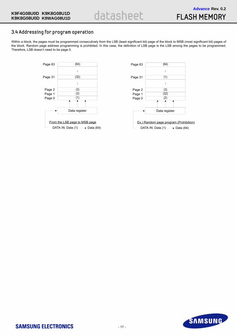
3.4 Addressing for program operation
Within a block, the pages must be programmed consecutively from the LSB (least significant bit) page of the block to MSB (most significant bit) pages of the block. Random page address programming is prohibited. In this case, the definition of LSB page is the LSB among the pages to be programmed. Therefore, LSB doesn’t need to be page 0.
From the LSB page to MSB page
DATA IN: Data (1) Data (64)
(1)(2)(3)
(32)
(64)
Data register
Page 0Page 1Page 2
Page 31
Page 63
Ex.) Random page program (Prohibition)
DATA IN: Data (1) Data (64)
(2)(32)(3)
(1)
(64)
Data register
Page 0Page 1Page 2
Page 31
Page 63
:
:
:
:

- 18 -
datasheetK9K8G08U0D FLASH MEMORYRev. 0.2Advance
K9F4G08U0D K9K8G08U1DK9WAG08U1D
3.5 System Interface Using CE don’t-care.
For an easier system interface, CE may be inactive during the data-loading or serial access as shown below. The internal 8,628byte data registers are utilized as separate buffers for this operation and the system design gets more flexible. In addition, for voice or audio applications which use slow cycle time in the order of μ-seconds, de-activating CE during the data-loading and serial access would provide significant savings in power consumption.
Program Operation with CE don’t-care
Read Operation with CE don’t-care
CE
WEtWP
tCHtCS
Address(5Cycles)80h Data Input
CE
CLE
ALE
WE
Data Input
CE don’t-care
10h
tCEA
out
tREA
CE
RE
I/O0~7
I/Ox
≈≈
≈≈
≈≈
≈≈
≈≈
≈ ≈
Address(5Cycle)00h
CE
CLE
ALE
WE
Data Output(serial access)
CE don’t-care
R/B tR
RE
30hI/Ox
≈
≈≈
≈≈
≈
≈≈
≈≈
≈
≈

- 19 -
datasheetK9K8G08U0D FLASH MEMORYRev. 0.2Advance
K9F4G08U0D K9K8G08U1DK9WAG08U1D
4.0 TIMING DIAGRAMS
4.1 Command Latch Cycle
4.2 Address Latch Cycle
CE
WE
CLE
ALE
Command
tCLS
tCS
tCLH
tCH
tWP
tALS tALH
tDS tDH
I/Ox
CE
WE
CLE
ALE
Col. Add1
tCStWC
tWP
tALS
tDStDH
tALH tALStWH
tWC
tWP
tDStDH
tALH tALStWH
tWC
tWP
tDStDH
tALH tALStWH
tDStDH
tWP
I/Ox Col. Add2 Row Add1 Row Add2
tWC
tWHtALH tALS
tDStDH
Row Add3
tALH
tCLS

- 20 -
datasheetK9K8G08U0D FLASH MEMORYRev. 0.2Advance
K9F4G08U0D K9K8G08U1DK9WAG08U1D
4.3 Input Data Latch Cycle
4.4 * Serial Access Cycle after Read(CLE=L, WE=H, ALE=L)
NOTE : 1) Transition is measured at ±200mV from steady state voltage with load. This parameter is sampled and not 100% tested.2) tRLOH is valid when frequency is higher than 20MHz. tRHOH starts to be valid when frequency is lower than 20MHz.
CE
CLE
WE
DIN 0 DIN 1 DIN final
ALE
tALS
tCLH
tWC
tCH
tDS tDH tDStDH
tDStDH
tWP
tWH
tWP tWP≈≈
≈I/Ox
≈≈
≈
RE
CE
R/B
Dout Dout Dout
tRC
tREA
tRR
tRHOH
tREAtREH
tREA
tRHZ
≈≈
≈≈
I/Ox
tCHZ
tRHZ

- 21 -
datasheetK9K8G08U0D FLASH MEMORYRev. 0.2Advance
K9F4G08U0D K9K8G08U1DK9WAG08U1D
4.5 Serial Access Cycle after Read(EDO Type, CLE=L, WE=H, ALE=L)
NOTE : 1) Transition is measured at ±200mV from steady state voltage with load. This parameter is sampled and not 100% tested.2) tRLOH is valid when frequency is higher than 20MHz. tRHOH starts to be valid when frequency is lower than 20MHz.
4.6 Status Read Cycle
RE
CE
R/B
I/Ox
≈
tRR
tCEA
tREA
tRP tREH
tRC
≈
tRHZ
tCHZ
tRHOHtRLOH
≈≈
Dout Dout
tREA
≈
CE
WE
CLE
RE
70h/F1h Status Output
tCLR
tCLH
tWPtCH
tDStDH tREAtIR
tRHOH
tWHR
tCEA
tCLS
I/Ox
tCHZ
tRHZ
tCS

- 22 -
datasheetK9K8G08U0D FLASH MEMORYRev. 0.2Advance
K9F4G08U0D K9K8G08U1DK9WAG08U1D
4.7 Read Operation
4.8 Read Operation(Intercepted by CE)
CE
CLE
R/B
WE
ALE
RE
Busy
00h Col. Add1 Col. Add2 Row Add1 Dout N Dout N+1
Column Address Row Address
tWBtAR
tR tRCtRHZ
tRR
Dout M
tWC
≈≈
≈
Row Add2 30h
tCLR
I/Ox Row Add3
CE
CLE
R/B
WE
ALE
RE
Busy
00h Dout N Dout N+1 Dout N+2
Row AddressColumn Address
tWB
tAR
tCHZ
tR
tRR
tRC
30hI/Ox Col. Add1 Col. Add2 Row Add1 Row Add2 Row Add3
tCLR
tCSD

- 23 -
datasheetK9K8G08U0D FLASH MEMORYRev. 0.2Advance
K9F4G08U0D K9K8G08U1DK9WAG08U1D
4.9 Random Data Output In a Page C
E
CLE R/BWE
ALE R
E
Busy
00h
Dout
NDo
ut N
+1
Row
Addr
ess
Colu
mn
Addr
ess
tWB
tAR
tR tRR
tRC
30h
05h
Colu
mn
Addr
ess
Dout
MDo
ut M
+1I/O
xC
ol. A
dd1
Col
. Add
2R
ow A
dd1
Row
Add2
Col
Add
1Co
l Add
2Ro
w Ad
d3E
0h
tRH
W
tCLR
tWH
R tRE
A
- 24 -
datasheetK9K8G08U0D FLASH MEMORYRev. 0.2Advance
K9F4G08U0D K9K8G08U1DK9WAG08U1D
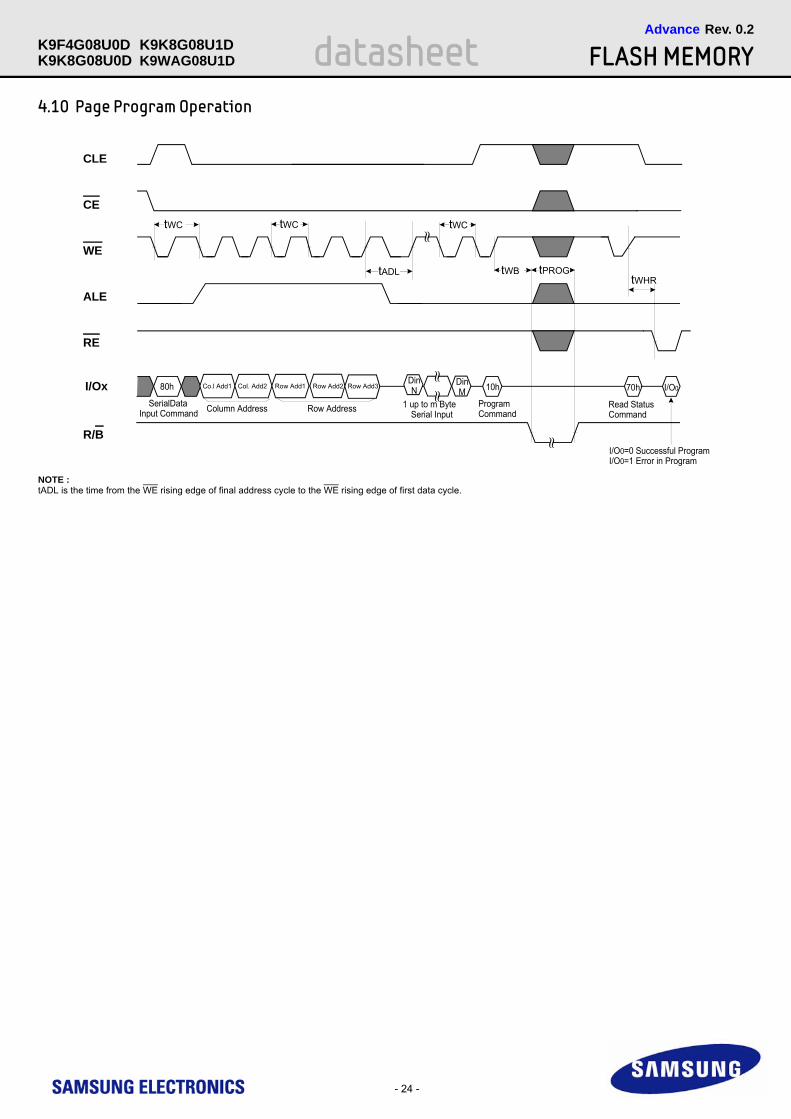
4.10 Page Program Operation
NOTE : tADL is the time from the WE rising edge of final address cycle to the WE rising edge of first data cycle.
CE
CLE
R/B
WE
ALE
RE
80h 70h I/O0DinN
Din 10hMSerialData
Input Command Column Address Row Address 1 up to m ByteSerial Input
ProgramCommand
Read StatusCommand
I/O0=0 Successful ProgramI/O0=1 Error in Program
tPROGtWB
tWC tWC tWC
≈≈
≈
≈
I/Ox Co.l Add1 Col. Add2 Row Add1 Row Add2 Row Add3
tADLtWHR
- 25 -
datasheetK9K8G08U0D FLASH MEMORYRev. 0.2Advance
K9F4G08U0D K9K8G08U1DK9WAG08U1D
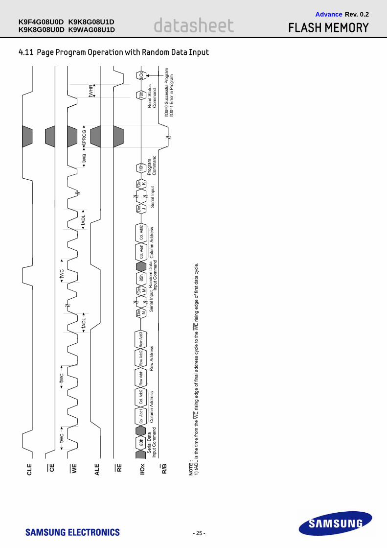
4.11 Page Program Operation with Random Data InputC
E
CLE R/BWE
ALE R
E
80h
70h
I/O0
Din N
Din
10h
MSe
rial D
ata
Inpu
t Com
man
dC
olum
n Ad
dres
sR
ow A
ddre
ssSe
rial I
nput
Prog
ram
Com
man
dR
ead
Stat
usC
omm
and
tPR
OG
tWB
tWC
tWC
≈ ≈
≈
≈
85h
Ran
dom
Dat
aIn
put C
omm
and
Col
umn
Addr
ess
tWC
Din J
Din K
Seria
l Inp
ut
≈ ≈
I/Ox
Col. A
dd1
Col. A
dd2
Row
Add1
Row
Add2
Col. A
dd1
Col. A
dd2
Row
Add3
≈
tAD
LtA
DL
tWH
R
I/O0=
0 Su
cces
sful
Pro
gram
I/O0=
1 Er
ror i
n Pr
ogra
m
NO
TE :
1) tA
DL
is th
e tim
e fro
m th
e W
E ri
sing
edg
e of
fina
l add
ress
cyc
le to
the
WE
risi
ng e
dge
of fi
rst d
ata
cycl
e.

- 26 -
datasheetK9K8G08U0D FLASH MEMORYRev. 0.2Advance
K9F4G08U0D K9K8G08U1DK9WAG08U1D
4.12 Copy-Back Program Operation
00h
I/Ox
85h
Colum
n Ad
dres
sRo
w Ad
dres
s R
ead
Stat
us C
omm
and
I/O0=
0 Su
cces
sful P
rogr
amI/O
0=1
Erro
r in
Prog
ram
tPR
OG
tWB
tWC
≈
Busy
tWB
tR
Busy
≈
10h
Copy
-Bac
k Da
taIn
put C
omm
and
35h
Colum
n Ad
dres
sRo
w Ad
dres
s
Data
1Da
ta N
≈≈
Col. A
dd1Co
l. Add2
Row A
dd1Ro
w Add2
Col. A
dd1Co
l. Add2
Row A
dd1Ro
w Add2
Row A
dd3Ro
w Add3
70h
tAD
L
tWH
R
Data
1Da
ta N
≈≈
tRC
CE
CLE
R/B
WE
ALE
RE
I/Ox
NO
TE :
1) t
ADL
is th
e tim
e fro
m th
e W
E ris
ing
edge
of f
inal
add
ress
cyc
le to
the
WE
risin
g ed
ge o
f firs
t dat
a cy
cle.

- 27 -
datasheetK9K8G08U0D FLASH MEMORYRev. 0.2Advance
K9F4G08U0D K9K8G08U1DK9WAG08U1D
4.13 Copy-Back Program Operation with Random Data Input
00h
I/Ox
85h
Colum
n Add
ress
Row
Addr
ess
Rea
d St
atus
Com
man
d
I/O0=
0 Su
cces
sful P
rogr
amI/O
0=1
Erro
r in
Prog
ram
tPR
OG
tWB
tWC
≈
Busy
tWB
tR
Busy
≈
10h
Copy
-Bac
k Da
taIn
put C
omm
and
35h
Colum
n Ad
dres
sRo
w Ad
dres
s
Data
1Da
ta N
≈≈
Col. A
dd1Co
l. Add2
Row A
dd1Ro
w Add2
Col. A
dd1Co
l. Add2
Row A
dd1Ro
w Add2
Row A
dd3Ro
w Add3
70h
tAD
L
tWH
R
Data
1Da
ta N
≈≈
tRC
CE
CLE R/BWE
ALE R
E
I/Ox
NO
TE :
1) t
ADL
is th
e tim
e fro
m th
e W
E ris
ing
edge
of f
inal
add
ress
cyc
le to
the
WE
risin
g ed
ge o
f firs
t dat
a cy
cle.

- 28 -
datasheetK9K8G08U0D FLASH MEMORYRev. 0.2Advance
K9F4G08U0D K9K8G08U1DK9WAG08U1D
4.14 Two-Plane Page Program Operation
80h
I/O0~
7
R/B
11h
Ex.)
Two-
Plan
e Pa
ge P
rogr
am
tDBS
Y
Add
ress
& D
ata
Inpu
t 8
1h10
h A
ddre
ss &
Dat
a In
put
70h/
F1h
tPR
OG
Col
Add
1,2
& R
ow A
dd 1
,2,3
8,62
8 B
yte
Dat
a
CE
CLE R/BWE
ALE R
E
80h
Din N
Din
11h
MSe
rial D
ata
Inp
ut C
omm
and
Colu
mn
Addr
ess
Prog
ram
tDB
SY
tWB
tWC
≈ ≈
≈
≈
Comm
and
(Dum
my)
Din N10
h
≈ ≈
≈
I/O
Prog
ram C
onfirm
Comm
and
(True
)
81h
70h/F
1h
Page
Row
Add
ress
I/Ox
≈
1 up
to 8
,628
Byt
e D
ata
Seria
l Inp
ut
Din MRe
ad S
tatus
Com
mand
tDB
SY :
t
yp. 5
00ns
m
ax. 1μs
Col A
dd1
Col A
dd2
Row A
dd1
Row A
dd2
Row A
dd3Co
l Add
1Co
l Add2
Row A
dd1
Row A
dd2Ro
w Add3
Col
Add
1,2
& R
ow A
dd 1
,2,3
8,62
8 B
yte
Dat
a
NO
TE :
Any
com
man
d be
twee
n 11
h an
d 81
h is
pro
hibi
ted
exce
pt 7
0h/F
1h a
nd F
Fh.
Not
e
tWH
R
I/O0=
1 Er
ror i
n Pr
ogra
mI/O
0=0
Succ
essf
ul P
rogr
am
tWB
tPR
OG

- 29 -
datasheetK9K8G08U0D FLASH MEMORYRev. 0.2Advance
K9F4G08U0D K9K8G08U1DK9WAG08U1D
4.15 Block Erase Operation
CE
CLE
R/B
WE
ALE
RE
60h
Erase CommandRead StatusCommand
I/O0=1 Error in Erase
D0h 70h I/O 0
Busy
tWB tBERS
I/O0=0 Successful Erase
Row Address
tWC
≈Auto Block EraseSetup Command
I/Ox Row Add1 Row Add2 Row Add3
tWHR

- 30 -
datasheetK9K8G08U0D FLASH MEMORYRev. 0.2Advance
K9F4G08U0D K9K8G08U1DK9WAG08U1D
4.16 Two-Plane Block Erase Operation
Blo
ck E
rase
Set
up C
omm
and1
Era
se C
onfir
m C
omm
and
Rea
d S
tatu
sC
omm
and
60h
Row
Add
1,2,
3
I/O0~
7
R/B
60h
A9
~ A
25D
0h
tBER
S
Ex.)
Add
ress
Res
tric
tion
for T
wo-
Plan
e B
lock
Era
se O
pera
tion
CE
CLE R/B
I/OX
WE
ALE R
E
60h
Row
Add
1D
0h70
h/F1
hI/O
0
Bus
y
tWB
tBE
RS
tWC
D0h
70h/
F1h
Addr
ess
Addr
ess
Row
Add
1,2,
3
I/O 0
= 0
Suc
cess
ful E
rase
I/O 0
= 1
Err
or in
Era
se
Row
Add
2R
ow A
dd3
60h
Row
Add
1D
0hR
ow A
dd2
Row
Add
3
Row
Add
ress
tWC
Blo
ck E
rase
Set
up C
omm
and2R
ow A
ddre
ss
tWH
R

- 31 -
datasheetK9K8G08U0D FLASH MEMORYRev. 0.2Advance
K9F4G08U0D K9K8G08U1DK9WAG08U1D
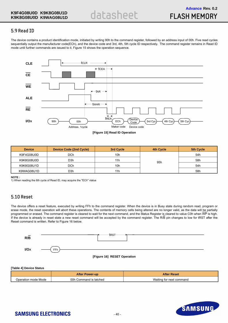
4.17 Read ID Operation
NOTE : 1) When reading the 6th cycle of Read ID, may acquire the "ECh" vlalue
Device Device Code (2nd Cycle) 3rd Cycle 4th Cycle 5th Cycle
K9F4G08U0D DCh 10h
95h
54h
K9K8G08U0D D3h 11h 58h
K9K8G08U1D DCh 10h 54h
K9WAG08U1D D3h 11h 58h
CE
CLE
WE
ALE
RE
90h
Read ID Command Maker Code Device Code
00h ECh
tREA
Address 1cycle
I/Ox
tAR
Device 4th cyc.Code 3rd cyc. 5th cyc. 6th cyc.

- 32 -
datasheetK9K8G08U0D FLASH MEMORYRev. 0.2Advance
K9F4G08U0D K9K8G08U1DK9WAG08U1D
3rd ID Data
4th ID Data
5th ID Data
Description
1st Byte2nd Byte3rd Byte4th Byte5th Byte
Maker CodeDevice CodeInternal Chip Number, Cell Type, Number of Simultaneously Programmed Pages, EtcPage Size, Block Size,Redundant Area Size, Organization, Serial Access MinimumPlane Number, Plane Size
Description I/O7 I/O6 I/O5 I/O4 I/O3 I/O2 I/O1 I/O0
Internal Chip Number
1 2 4 8
0 0 0 1 1 0 1 1
Cell Type
2 Level Cell 4 Level Cell 8 Level Cell 16 Level Cell
0 0 0 1 1 0 1 1
Number of Simultaneously Programmed Pages
1 2 4 8
0 0 0 1 1 0 1 1
Interleave ProgramBetween multiple chips
Not Support Support
0 1
Cache Program Not Support Support
0 1
Description I/O7 I/O6 I/O5 I/O4 I/O3 I/O2 I/O1 I/O0
Page Size (w/o redundant area )
1KB 2KB 4KB 8KB
0 00 11 01 1
Block Size (w/o redundant area )
64KB128KB256KB512KB
0 0 0 1 1 0 1 1
Redundant Area Size ( byte/512byte)
8 16
01
Organization x8 x16
01
Serial Access Minimum
50ns/30ns25nsReservedReserved
0101
0101
Description I/O7 I/O6 I/O5 I/O4 I/O3 I/O2 I/O1 I/O0
Plane Number
1 2 4 8
0 0 0 1 1 0 1 1
Plane Size (w/o redundant Area)
64Mb128Mb256Mb512Mb1Gb2Gb4Gb8Gb
0 0 0 0 0 1 0 1 0 0 1 1 1 0 0 1 0 1 1 1 0 1 1 1
Reserved 0 0 0

- 33 -
datasheetK9K8G08U0D FLASH MEMORYRev. 0.2Advance
K9F4G08U0D K9K8G08U1DK9WAG08U1D
5.0 DEVICE OPERATION
[Figure 4] Read Operation
5.1 Page Read
Page read is initiated by writing 00h-30h to the command register along with five address cycles. After initial power up, 00h command is latched. There-fore only five address cycles and 30h command initiates that operation after initial power up. The 2,112 bytes of data within the selected page are trans-ferred to the data registers in less than 25μs(tR). The system controller can detect the completion of this data transfer(tR) by analyzing the output of R/Bpin. Once the data in a page is loaded into the data registers, they may be read out in 25ns cycle time by sequentially pulsing RE. The repetitive high to low transitions of the RE clock make the device output the data starting from the selected column address up to the last column address. The device may output random data in a page instead of the consecutive sequential data by writing random data output command. The column address of next data, which is going to be out, may be changed to the address which follows random data output command. Random data output can be operated multiple times regardless of how many times it is done in a page.
Address(5Cycle)00h
Col. Add.1,2 & Row Add.1,2,3
Data Output(Serial Access)
Data Field Spare Field
CE
CLE
ALE
R/B
WE
RE
tR
30hI/Ox
≈≈
≈≈
≈≈

[Figure 5] Random Data Output In a Page
[Figure 6] Program & Read Status Operation
- 34 -
datasheetK9K8G08U0D FLASH MEMORYRev. 0.2Advance
K9F4G08U0D K9K8G08U1DK9WAG08U1D
5.2 Page Program
The device is programmed basically on a page basis, but it does allow multiple partial page programming of a word or consecutive bytes up to 2,112, in a single page program cycle. The number of consecutive partial page programming operation within the same page without an intervening erase operation must not exceed 4 times for a single page. The addressing should be done in sequential order in a block. A page program cycle consists of a serial data loading period in which up to 2,112bytes of data may be loaded into the data register, followed by a non-volatile programming period where the loaded data is programmed into the appropriate cell. The serial data loading period begins by inputting the Serial Data Input command(80h), followed by the five cycle address inputs and then serial data loading. The words other than those to be programmed do not need to be loaded. The device supports random data input in a page. The column address for the next data, which will be entered, may be changed to the address which follows random data input command(85h). Random data input may be operated multiple times regardless of how many times it is done in a page. The Page Program confirm command(10h) initiates the programming process. Writing 10h alone without previously entering the serial data will not initiate the programming process. The internal write state controller automatically exe-cutes the algorithms and timings necessary for program and verify, thereby freeing the system controller for other tasks. Once the program process starts, the Read Status Register command may be entered to read the status register. The system controller can detect the completion of a program cycle by monitoring the R/B output, or the Status bit(I/O 6) of the Status Register. Only the Read Status command and Reset command are valid while program-ming is in progress. When the Page Program is complete, the Write Status Bit(I/O 0) may be checked(Figure 6). The internal write verify detects only errors for "1"s that are not successfully programmed to "0"s. The command register remains in Read Status command mode until another valid command is written to the command register.
Address00h Data Output
R/B
RE
tR
30h Address05h E0h5Cycles 2Cycles Data Output
Data Field Spare Field Data Field Spare Field
I/Ox
Col. Add.1,2 & Row Add.1,2,3 Col. Add.1,2
80h
R/B
Address & Data Input I/O0 Pass
Data
10h 70h
Fail
tPROG
I/OxCol. Add.1,2 & Row Add.1,2,3
"0"
"1"

[Figure 7] Random Data Input In a Page
[Figure 9] Page Copy-Back Program Operation with Random Data Input
[Figure 8] Page Copy-Back Program Operation
- 35 -
datasheetK9K8G08U0D FLASH MEMORYRev. 0.2Advance
K9F4G08U0D K9K8G08U1DK9WAG08U1D
5.3 Copy-back Program
Copy-Back program with Read for Copy-Back is cond to quickly and efficiently rewrite data stored in one page without data re-loading when the bit error is not in data stored. Since the time-consuming re-loading cycles are removed, the system performance is improved. The benefit is especially obvious when a portion of a block is updated and the rest of the block also needs to be copied to the newly assigned free block. Copy-Back operation is a sequen-tial execution of Read for Copy-Back and of copy-back program with the destination page address. A read operation with "35h" command and the address of the source page moves the whole 2,112-byte data into the internal data buffer. A bit error is checked by sequential reading the data output. In the case where there is no bit error, the data do not need to be reloaded. Therefore Copy-Back program operation is initiated by issuing Page-Copy Data-Input command (85h) with destination page address. Actual programming operation begins after Program Confirm command (10h) is issued. Once the program process starts, the Read Status Register command (70h) may be entered to read the status register. The system controller can detect the com-pletion of a program cycle by monitoring the R/B output, or the Status bit(I/O 6) of the Status Register. When the Copy-Back Program is complete, the Write Status Bit(I/O 0) may be checked(Figure 8 & Figure 9). The command register remains in Read Status command mode until another valid com-mand is written to the command register.During copy-back program, data modification is possible using random data input command (85h) as shown in Figure 9.
80h
R/B
Address & Data Input I/O0 Pass10h 70h
Fail
tPROG
85h Address & Data InputI/OxCol. Add.1,2 & Row Add1,2,3 Col. Add.1,2
Data Data
"0"
"1"
"0"
"1"
00h
R/B
Add.(5Cycles) I/O0 Pass
Fail
tPROGtR
Source Address Destination Address
I/OxCol. Add.1,2 & Row Add.1,2,3Col. Add.1,2 & Row Add.1,2,3
35h Data Output 85h Add.(5Cycles) 10h 70h
≈≈
R/B
Source Address Destination Address There is no limitation for the number of repetition.
I/OxCol. Add.1,2 & Row Add.1,2,3 Col. Add.1,2 & Row Add.1,2,3 Col. Add.1,2
00h Add.(5Cycles) 35h
tR
Data Output 85h Add.(5Cycles) Data
≈≈
85h Add.(2Cycles) Data 10h
tPROG
70h

[Figure 10] Block Erase Operation
[Figure 11] Two-Plane Page Program
- 36 -
datasheetK9K8G08U0D FLASH MEMORYRev. 0.2Advance
K9F4G08U0D K9K8G08U1DK9WAG08U1D
5.4 Block Erase
The Erase operation is done on a block basis. Block address loading is accomplished in three cycles initiated by an Erase Setup command(60h). Only address A18 to A29 is valid while A12 to A17 is ignored. The Erase Confirm command(D0h) following the block address loading initiates the internal erasing process. This two-step sequence of setup followed by execution command ensures that memory contents are not accidentally erased due to external noise conditions.At the rising edge of WE after the erase confirm command input, the internal write controller handles erase and erase-verify. When the erase operation is completed, the Write Status Bit(I/O 0) may be checked. Figure 10 details the sequence.
5.5 Two-plane Page Program
Two-Plane Page Program is an extension of Page Program, for a single plane with 2112 byte page registers. Since the device is equipped with two mem-ory planes, activating the two sets of 2112 byte page registers enables a simultaneous programming of two pages. After writing the first set of data up to 2112 byte into the selected page register, Dummy Page Program command (11h) instead of actual Page Program command (10h) is inputted to finish data-loading of the first plane. Since no programming process is involved, R/B remains in Busy state for a short period of time(tDBSY). Read Status command (70h/F1h) may be issued to find out when the device returns to Ready state by polling the Ready/Busy status bit(I/O 6). Then the next set of data for the other plane is inputted after the 81h command and address sequences. After inputting data for the last plane, actual True Page Program(10h) instead of dummy Page Program command (11h) must be followed to start the programming process. The operation of R/B and Read Status is the same as that of Page Program. Althougth two planes are programmed simultaneously, pass/fail is not available for each page when the program operation completes. Status bit of I/O 0 is set to "1" when any of the pages fails. Restriction in addressing with Two-Plane Page Program is shown is Figure 11.
60h
Row Add 1,2,3
R/B
Address Input(3Cycle) I/O0 PassD0h 70h
Fail
tBERS
I/Ox"0"
"1"
80h 11hDataInput
Plane 0(2048 Block)
Block 0Block 2
Block 4094Block 4092
80hI/O0 ~ 7
R/B
Address & Data Input 11h 81h 10h
tDBSY tPROG
70h/F1h Address & Data Input
NOTE :1. It is noticeable that same row address except for A18 is applied to the two blocks
81h 10h
Plane 1(2048 Block)
Block 1Block 3
Block 4095Block 4093
A0 ~ A11 : ValidA12 ~ A17 : Fixed ’Low’A18 : Fixed ’Low’A19 ~ A29 : Fixed ’Low’
A0 ~ A11 : ValidA12 ~ A17 : ValidA18 : Fixed ’High’A19 ~ A29 : Valid
2. Any command between 11h and 81h is prohibited except 70h/F1h and FFh.
Note*2

[Figure 12] Two-Plane Block Erase Operation
[Figure 13] Two-Plane Copy-Back Program Operation
- 37 -
datasheetK9K8G08U0D FLASH MEMORYRev. 0.2Advance
K9F4G08U0D K9K8G08U1DK9WAG08U1D
5.6 Two-plane Block Erase
Basic concept of Two-Plane Block Erase operation is identical to that of Two-Plane Page Program. Up to two blocks, one from each plane can be simul-taneously erased. Standard Block Erase command sequences (Block Erase Setup command(60h) followed by three address cycles) may be repeated up to twice for erasing up to two blocks. Only one block should be selected from each plane. The Erase Confirm command(D0h) initiates the actual erasing process. The completion is detected by monitoring R/B pin or Ready/Busy status bit (I/O 6).
5.7 Two-plane Copy-back Program
Two-Plane Copy-Back Program is an extension of Copy-Back Program, for a single plane with 2112 byte page registers. Since the device is equipped with two memory planes, activating the two sets of 2112 byte page registers enables a simultaneous programming of two pages.
NOTE : 1) Copy-Back Program operation is allowed only within the same memory plane.2) Any command between 11h and 81h is prohibited except 70h/F1h and FFh.
60hI/OX
R/B
60h D0h I/O0 Pass
Fail
tBERS
Address (3 Cycle) Address (3 Cycle) 70h/F1h"0"
"1"A12 ~ A17 : Fixed ’Low’A18 :Fixed ’Low’A19 ~ A29 : Fixed ’Low’
A12 ~ A17 : Fixed ’Low’A18 : Fixed ’High’A19 ~ A29 : valid
00h
R/B
Add.(5Cycles)
tR
Source Address On Plane0
35hI/OxCol. Add.1,2 & Row Add.1,2,3
1
R/B
85h 70h/F1h
tPROG
Add.(5Cycles)
Destination Address
10hI/Ox
Col. Add.1,2 & Row Add.1,2,3
81h Add.(5Cycles)
Destination AddressCol. Add.1,2 & Row Add.1,2,3
11h
tDBSY
A0 ~ A11 : Fixed ’Low’A12 ~ A17 : ValidA18 : Fixed ’High’A19 ~ A29 : Valid
1Note2
A0 ~ A11 : Fixed ’Low’A12 ~ A17 : Fixed ’Low’A18 : Fixed ’Low’A19 ~ A29 : Fixed ’Low’
Data Field Spare Field Data Field Spare Field
(1) (2)(3) (3)
Plane0 Plane1
Source page
Target page
Source page
Target page (1) : Read for Copy Back On Plane0
(2) : Read for Copy Back On Plane1
(3) : Two-Plane Copy-Back Program
00h Add.(5Cycles)
Source Address On Plane1
35h
Col. Add.1,2 & Row Add.1,2,3
tR
Data OutputData Output
≈≈
≈≈

[Figure 14] Two-Plane Copy-Back Program Operation with Random Data Input
- 38 -
datasheetK9K8G08U0D FLASH MEMORYRev. 0.2Advance
K9F4G08U0D K9K8G08U1DK9WAG08U1D
NOTE: 1) Copy-Back Program operation is allowed only within the same memory plane.2) Any command between 11h and 81h is prohibited except 70h/F1h and FFh.
R/B
85h 11h
tDBSY
Add.(5Cycles) Data 85h DataI/OxCol. Add.1,2 & Row Add.1,2,3 Col. Add.1,2
Add.(2Cycles)
00h
R/B
Add.(5Cycles)
tR
Source Address On Plane0
35hI/OxCol. Add.1,2 & Row Add.1,2,3
1
R/B
81h 10h
tPROG
Add.(5Cycles) Data 85h DataI/OxCol. Add.1,2 & Row Add.1,2,3 Col. Add.1,2
Add.(2Cycles)
1 2
2
Destination AddressA0 ~ A11 : ValidA12 ~ A17 : Fixed ’Low’A18 : Fixed ’Low’A19 ~ A29 : Fixed ’Low’
Destination AddressA0 ~ A11 : ValidA12 ~ A17 : ValidA18 : Fixed ’High’A19 ~ A29 : Valid
Note2
00h Add.(5Cycles)
Source Address On Plane1
35h
Col. Add.1,2 & Row Add.1,2,3
tR
Data OutputData Output
≈≈
≈≈

- 39 -
datasheetK9K8G08U0D FLASH MEMORYRev. 0.2Advance
K9F4G08U0D K9K8G08U1DK9WAG08U1D
5.8 Read Status
The device contains a Status Register which may be read to find out whether program or erase operation is completed, and whether the program or erase operation is completed successfully. After writing 70h/F1h command to the command register, a read cycle outputs the content of the Status Register to the I/O pins on the falling edge of CE or RE, whichever occurs last. This two line control allows the system to poll the progress of each device in multiple memory connections even when R/B pins are common-wired. RE or CE does not need to be toggled for updated status. Refer to Table 2 for specific Sta-tus Register definitions and Table 3 for specific F1h Status Register definitions. The command register remains in Status Read mode until further com-mands are issued to it. Therefore, if the status register is read during a random read cycle, the read command(00h) should be given before starting read cycles.
[Table 2] Status Register Definition for 70h Command
NOTE : 1) I/Os defined ’Not use’ are recommended to be masked out when Read Status is being executed.
[Table 3] Status Register Definition for F1h Command
NOTE : 1) I/Os defined ’Not use’ are recommended to be masked out when Read Status is being executed.
I/O Page Program Block Erase Read Definition
I/O 0 Pass/Fail Pass/Fail Not use Pass : "0" Fail : "1"
I/O 1 Not use Not use Not use Don’t -cared
I/O 2 Not use Not use Not use Don’t -cared
I/O 3 Not Use Not Use Not Use Don’t -cared
I/O 4 Not Use Not Use Not Use Don’t -cared
I/O 5 Not Use Not Use Not Use Don’t -cared
I/O 6 Ready/Busy Ready/Busy Ready/Busy Busy : "0" Ready : "1"
I/O 7 Write Protect Write Protect Write Protect Protected : "0" Not Protected : "1"
I/O No. Page Program Block Erase Read Definition
I/O 0 Chip Pass/Fail Chip Pass/Fail Not use Pass : "0" Fail : "1"
I/O 1 Plane0 Pass/Fail Plane0 Pass/Fail Not use Pass : "0" Fail : "1"
I/O 2 Plane1 Pass/Fail Plane1 Pass/Fail Not use Pass : "0" Fail : "1"
I/O 3 Not Use Not Use Not Use Don’t -cared
I/O 4 Not Use Not Use Not Use Don’t -cared
I/O 5 Not Use Not Use Not Use Don’t -cared
I/O 6 Ready/Busy Ready/Busy Ready/Busy Busy : "0" Ready : "1"
I/O 7 Write Protect Write Protect Write Protect Protected : "0" Not Protected : "1" "1"otected
[Figure 15] Read ID Operation
[Figure 16] RESET Operation
- 40 -
datasheetK9K8G08U0D FLASH MEMORYRev. 0.2Advance
K9F4G08U0D K9K8G08U1DK9WAG08U1D
5.9 Read ID
The device contains a product identification mode, initiated by writing 90h to the command register, followed by an address input of 00h. Five read cycles sequentially output the manufacturer code(ECh), and the device code and 3rd, 4th, 5th cycle ID respectively. The command register remains in Read ID mode until further commands are issued to it. Figure 15 shows the operation sequence.
NOTE :1) When reading the 6th cycle of Read ID, may acquire the "ECh" vlalue
5.10 Reset
The device offers a reset feature, executed by writing FFh to the command register. When the device is in Busy state during random read, program or erase mode, the reset operation will abort these operations. The contents of memory cells being altered are no longer valid, as the data will be partially programmed or erased. The command register is cleared to wait for the next command, and the Status Register is cleared to value C0h when WP is high. If the device is already in reset state a new reset command will be accepted by the command register. The R/B pin changes to low for tRST after the Reset command is written. Refer to Figure 16 below.
[Table 4] Device Status
Device Device Code (2nd Cycle) 3rd Cycle 4th Cycle 5th Cycle
K9F4G08U0D DCh 10h
95h
54h
K9K8G08U0D D3h 11h 58h
K9K8G08U1D DCh 10h 54h
K9WAG08U1D D3h 11h 58h
After Power-up After Reset
Operation mode Mode 00h Command is latched Waiting for next command
CE
CLE
I/OX
ALE
RE
WE
90h 00h
Address. 1cycle Maker code Device code
tCEA
tAR
tREA
tWHR
tCLR
Device4th Cyc.CodeECh 3rd Cyc. 5th Cyc.
FFhI/OX
R/BtRST
[Figure 17] Rp vs tr ,tf & Rp vs ibusy
- 41 -
datasheetK9K8G08U0D FLASH MEMORYRev. 0.2Advance
K9F4G08U0D K9K8G08U1DK9WAG08U1D
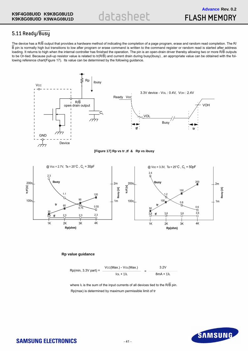
5.11 Ready/Busy
The device has a R/B output that provides a hardware method of indicating the completion of a page program, erase and random read completion. The R/B pin is normally high but transitions to low after program or erase command is written to the command register or random read is started after address loading. It returns to high when the internal controller has finished the operation. The pin is an open-drain driver thereby allowing two or more R/B outputs to be Or-tied. Because pull-up resistor value is related to tr(R/B) and current drain during busy(ibusy) , an appropriate value can be obtained with the fol-lowing reference chart(Figure 17). Its value can be determined by the following guidance.
VCC
R/Bopen drain output
Device
GND
Rp ibusy
Busy
Ready Vcc
VOH
tf tr
VOL
3.3V device - VOL : 0.4V, VOH : 2.4V
CL
tr,tf
[s]
Ibus
y [A
]
where IL is the sum of the input currents of all devices tied to the R/B pin.
Rp value guidance
Rp(max) is determined by maximum permissible limit of tr
Rp(min, 3.3V part) =VCC(Max.) - VOL(Max.)
IOL + ΣIL =
3.2V
8mA + ΣIL
Rp(ohm)
Ibusy
tr
@ Vcc = 3.3V, Ta = 25°C , CL = 50pF
1K 2K 3K 4K
100n
200n 2m
1m
50
tf
100
150
200
3.6 3.6 3.6 3.6
2.4
1.2
0.8
0.6
tr,tf
[s]
Ibus
y [A
]
Rp(ohm)
Ibusy
tr
@ Vcc = 2.7V, Ta = 25°C , CL = 30pF
1K 2K 3K 4K
100n
200n 2m
1m
30tf
60
90
120
2.3 2.3 2.3 2.3
2.3
1.1
0.75 0.55

[Figure 18] AC Waveforms for Power Transition
- 42 -
datasheetK9K8G08U0D FLASH MEMORYRev. 0.2Advance
K9F4G08U0D K9K8G08U1DK9WAG08U1D
5.12 Data Protection & Power Up Sequence
The device is designed to offer protection from any involuntary program/erase during power-transitions. An internal voltage detector disables all functions whenever Vcc is below about 2V(3.3V device). WP pin provides hardware protection and is recommended to be kept at VIL during power-up and power-down. A recovery time of minimum 100μs is required before internal circuit gets ready for any command sequences as shown in Figure 18. The two step command sequence for program/erase provides additional software protection.
NOTE :During the initialization, the device consumes a maximum current of 30mA (ICC1)
VCC
WP
High
≈≈
WE≈
≈≈Ready/Busy
5 ms max Operation
100μs
~ 2.3V ~ 2.3V
Invalid Don’t care
Don’t care