advanced electronic packaging - nasapackaging house ibm kyocera (us) bumping house spil then amkor...
TRANSCRIPT
Advanced Electronic PackagingThe Assurance Challenges
National Aeronautics and Space Administration
www.nasa.gov
October 15, 2013
Michael J. [email protected]
NASA Goddard Spaceflight Center (Greenbelt)Safety and Mission Assurance Directorate
301-614-6233Co- Manager NEPP Programhttp://nepp.nasa.gov
To be presented by Michael J. Sampson at the Trilateral NASA/Japan Aerospace Exploration Agency (JAXA)/European Space Agency (ESA) Safety and Mission Assurance Meeting, Washington, DC, October 15, 2013. 1
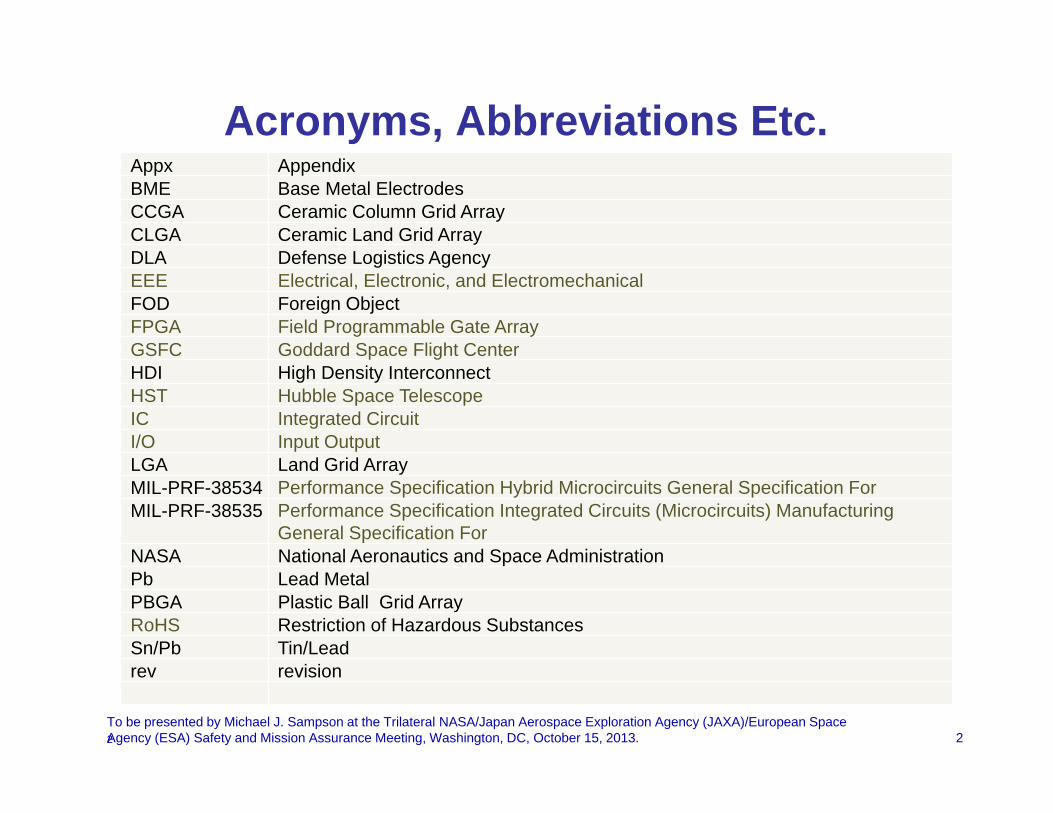
Acronyms, Abbreviations Etc.
2
Appx AppendixBME Base Metal ElectrodesCCGA Ceramic Column Grid ArrayCLGA Ceramic Land Grid ArrayDLA Defense Logistics AgencyEEE Electrical, Electronic, and ElectromechanicalFOD Foreign Object FPGA Field Programmable Gate ArrayGSFC Goddard Space Flight CenterHDI High Density InterconnectHST Hubble Space TelescopeIC Integrated CircuitI/O Input OutputLGA Land Grid ArrayMIL-PRF-38534 Performance Specification Hybrid Microcircuits General Specification ForMIL-PRF-38535 Performance Specification Integrated Circuits (Microcircuits) Manufacturing
General Specification ForNASA National Aeronautics and Space AdministrationPb Lead MetalPBGA Plastic Ball Grid ArrayRoHS Restriction of Hazardous SubstancesSn/Pb Tin/Leadrev revision
To be presented by Michael J. Sampson at the Trilateral NASA/Japan Aerospace Exploration Agency (JAXA)/European Space Agency (ESA) Safety and Mission Assurance Meeting, Washington, DC, October 15, 2013. 2
3
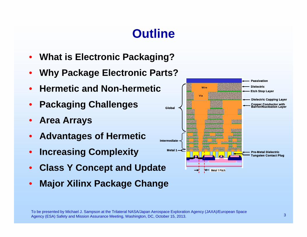
Outline
• What is Electronic Packaging?• Why Package Electronic Parts?• Hermetic and Non-hermetic• Packaging Challenges• Area Arrays• Advantages of Hermetic• Increasing Complexity• Class Y Concept and Update• Major Xilinx Package Change
Global
Intermediate
Metal 1
Passivation
DielectricEtch Stop Layer
Dielectric Capping LayerCopper Conductor with Barrier/Nucleation Layer
Pre-Metal Dielectric
Metal 1 Pitch
Tungsten Contact Plug
Via
Wire
Global
Intermediate
Metal 1
Passivation
DielectricEtch Stop Layer
Dielectric Capping LayerCopper Conductor with Barrier/Nucleation Layer
Pre-Metal Dielectric
Metal 1 Pitch
Tungsten Contact Plug
Via
Wire
To be presented by Michael J. Sampson at the Trilateral NASA/Japan Aerospace Exploration Agency (JAXA)/European Space Agency (ESA) Safety and Mission Assurance Meeting, Washington, DC, October 15, 2013.

What is Electronic Packaging?
• Within NASA, electronic “packaging” can have two basic meanings:– First (Part) Level: The “envelope” of protection
surrounding an active electronic element, and also the termination system to connect it to the outside world
– Second and Higher Levels: The assembly of parts to boards, boards to slices, slices to boxes, boxes to systems, instruments and spacecraft
• This discussion focuses on the first
4To be presented by Michael J. Sampson at the Trilateral NASA/Japan Aerospace Exploration Agency (JAXA)/European Space Agency (ESA) Safety and Mission Assurance Meeting, Washington, DC, October 15, 2013.

Why Package Electronic Parts?• To protect the active element against:
– Handling– Shock and vibration– Contamination– Light penetration or emission
• To provide a suitable system to make connection between the element and the printed wiring board
• To prevent conductive parts of the element from coming in contact with other conductive surfaces, unless intended
5
Active Element (Die)Envelope: Glass, Ceramic or Plastic
DIODETo be presented by Michael J. Sampson at the Trilateral NASA/Japan Aerospace Exploration Agency (JAXA)/European Space Agency (ESA) Safety and Mission Assurance Meeting, Washington, DC, October 15, 2013.
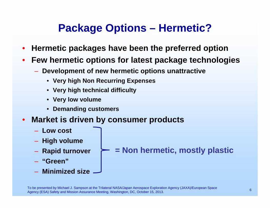
Package Options – Hermetic?
• Hermetic packages have been the preferred option• Few hermetic options for latest package technologies
– Development of new hermetic options unattractive• Very high Non Recurring Expenses• Very high technical difficulty• Very low volume• Demanding customers
• Market is driven by consumer products– Low cost– High volume– Rapid turnover– “Green”– Minimized size
6
= Non hermetic, mostly plastic
To be presented by Michael J. Sampson at the Trilateral NASA/Japan Aerospace Exploration Agency (JAXA)/European Space Agency (ESA) Safety and Mission Assurance Meeting, Washington, DC, October 15, 2013.

Continuous Packaging Challenges
• I/O s, increasing number, decreasing pitch• Heat Dissipation, (especially in space)• Manufacturability• Materials• Mechanical• Installation• Testability• Inspectability• RoHS (Pb-free)• (Space Environment)
Lunar Reconnaissance Orbiter (LRO), Built at GSFC, Launched with LCROSS, June 18,2009
7To be presented by Michael J. Sampson at the Trilateral NASA/Japan Aerospace Exploration Agency (JAXA)/European Space Agency (ESA) Safety and Mission Assurance Meeting, Washington, DC, October 15, 2013.
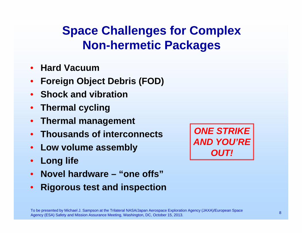
Space Challenges for Complex Non-hermetic Packages
• Hard Vacuum• Foreign Object Debris (FOD)• Shock and vibration• Thermal cycling• Thermal management• Thousands of interconnects• Low volume assembly• Long life• Novel hardware – “one offs”• Rigorous test and inspection
ONE STRIKE AND YOU’RE
OUT!
8To be presented by Michael J. Sampson at the Trilateral NASA/Japan Aerospace Exploration Agency (JAXA)/European Space Agency (ESA) Safety and Mission Assurance Meeting, Washington, DC, October 15, 2013.
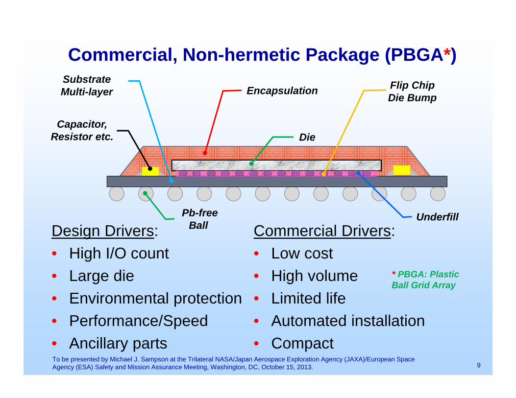
Commercial, Non-hermetic Package (PBGA*)
Design Drivers:• High I/O count• Large die• Environmental protection• Performance/Speed• Ancillary parts
Commercial Drivers:• Low cost• High volume• Limited life• Automated installation• Compact
Die
Underfill
Flip Chip Die Bump
Capacitor, Resistor etc.
SubstrateMulti-layer Encapsulation
Pb-free Ball
9
* PBGA: Plastic Ball Grid Array
To be presented by Michael J. Sampson at the Trilateral NASA/Japan Aerospace Exploration Agency (JAXA)/European Space Agency (ESA) Safety and Mission Assurance Meeting, Washington, DC, October 15, 2013.

Non-hermetic Package, With”Space” Features(CCGA*?)
Space Challenge Some DefensesVacuum Low out/off-gassing materials. Ceramics vs polymers.
Shock and vibration Compliant / robust interconnects - wire bonds, solder balls, columns, conductive polymer
Thermal cycling Compliant/robust interconnects, matched thermal expansion coefficients
Thermal management Heat spreader in the lid and/or substrate, thermally conductive materials
Thousands of interconnects
Process control, planarity, solderability, substrate design
Low volume assembly Remains a challenge
Long life Good design, materials, parts and process control
Novel hardware Test, test, test
Rigorous test and inspection
Testability and inspectability will always be challenges
CoverDie
Flip Chip Die Bump
Capacitor, Resistor etc.
“Enclosed” Package OptionUnderfill
Substrate and Sn/Pb Column
Grid Array
10
* Ceramic Column Grid Array
To be presented by Michael J. Sampson at the Trilateral NASA/Japan Aerospace Exploration Agency (JAXA)/European Space Agency (ESA) Safety and Mission Assurance Meeting, Washington, DC, October 15, 2013.

Hermeticity• NASA prefers hermetic packages for critical
applications• Hermeticity is measureable, assuring package
integrity – although testing is difficult• Just 3 tests provide assurance for hermetic
package integrity:– Hermeticity – nothing bad can get in– Residual or Internal gas analysis – nothing bad is inside– Particle Impact Noise Detection – no FOD inside
• NON-HERMETIC PACKAGE INTEGRITY IS HARD TO ASSESS - NO 3 BASIC TESTS
• Non-hermetic packages expose materials interfaces that are locked away in hermetic ones
11To be presented by Michael J. Sampson at the Trilateral NASA/Japan Aerospace Exploration Agency (JAXA)/European Space Agency (ESA) Safety and Mission Assurance Meeting, Washington, DC, October 15, 2013.

But What is Hermetic?• Per MIL-PRF-38534 Appx E and 38535 Appx A,
hermetic packages must consist of metals, ceramic and glass in combinations ONLY, no polymerics
• Meets aggressive leak rate test limits– Verifies low rate of gas escape/ atmospheric interchange– Even so, small volume packages meeting “tight limits”
theoretically exchange their atmosphere very quickly:• 0.001 cc, exchanges 93% in 1 month at 5X10⁻⁸ atmosphere/cc/sec!• 1.0cc, 96% in 10 years at 1 X 10⁻⁸
– Even large packages with quite small leaks can surprise• 10 cc, 96% in 1 year at 1 X 10⁻⁶ !
• For applications in space vacuum why care?– Risk for contamination on the ground– Risk for outgassing in vacuum
12To be presented by Michael J. Sampson at the Trilateral NASA/Japan Aerospace Exploration Agency (JAXA)/European Space Agency (ESA) Safety and Mission Assurance Meeting, Washington, DC, October 15, 2013.

Non-hermetic Package Variations• Current and future package options mix and match
elements in almost infinite combinations• Elements include:
– Wire bonds– Ball interconnects (flip chip)– Solder joints– Conductive epoxies– Vias– Multi-layer substrates– Multiple chips, active and passive (hybrid?)– Stacking of components– Embedded actives and passives– Polymers– Ceramics– Enclosures/encapsulants – Thermal control features– ETCETERA
13To be presented by Michael J. Sampson at the Trilateral NASA/Japan Aerospace Exploration Agency (JAXA)/European Space Agency (ESA) Safety and Mission Assurance Meeting, Washington, DC, October 15, 2013.
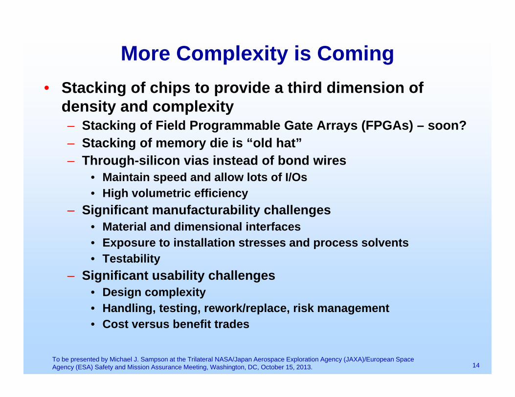
More Complexity is Coming• Stacking of chips to provide a third dimension of
density and complexity– Stacking of Field Programmable Gate Arrays (FPGAs) – soon?– Stacking of memory die is “old hat”– Through-silicon vias instead of bond wires
• Maintain speed and allow lots of I/Os• High volumetric efficiency
– Significant manufacturability challenges • Material and dimensional interfaces• Exposure to installation stresses and process solvents• Testability
– Significant usability challenges• Design complexity• Handling, testing, rework/replace, risk management• Cost versus benefit trades
14To be presented by Michael J. Sampson at the Trilateral NASA/Japan Aerospace Exploration Agency (JAXA)/European Space Agency (ESA) Safety and Mission Assurance Meeting, Washington, DC, October 15, 2013.

15
http://www.amkor.com/go/packaging
To be presented by Michael J. Sampson at the Trilateral NASA/Japan Aerospace Exploration Agency (JAXA)/European Space Agency (ESA) Safety and Mission Assurance Meeting, Washington, DC, October 15, 2013.

MIL-PRF-38535, Class Y• Space grade but non-hermetic – Class Y• New class for M38535, monolithic microcircuits• Class V will be defined as space-grade, hermetic only• Addition to Appendix B, “Space Application”• Package-specific “integrity” test requirements proposed by
manufacturer, approved by DLA* and government space• The Package Integrity Test Plan must address:
– Potential materials degradation– Interconnect reliability– Thermal management– Resistance to processing stresses– Thermo-mechanical stresses
• Allows great flexibility in package style• Final draft of M38535K in final review
16
* MIL spec qualifying activity Defense Logistics Agency, Land and Maritime
To be presented by Michael J. Sampson at the Trilateral NASA/Japan Aerospace Exploration Agency (JAXA)/European Space Agency (ESA) Safety and Mission Assurance Meeting, Washington, DC, October 15, 2013.

Current Sticky Points• Use of Base Metal Electrode (BME) capacitors
– Used for decoupling in Xilinx, Virtex 4 and 5 FPGAs– Increasingly used with high speed integrated circuits– Not yet accepted by US space users
• Electrical testing post column attach (for CCGAs)– Very difficult without causing destructive damage– Room temperature electricals perhaps– But tri temperature electricals and burn-in? NO
• Solder bump and column attachment testing– Shear, pull etc.
• And others• Trying to find compromise resolutions but could
further delay revision K• Until rev K is released, MIL certification audits cannot
occur and the “hidden” problems cannot be seen
To be presented by Michael J. Sampson at the Trilateral NASA/Japan Aerospace Exploration Agency (JAXA)/European Space Agency (ESA) Safety and Mission Assurance Meeting, Washington, DC, October 15, 2013. 17

Potential Class Y Suppliers
• The front runners– Aeroflex : – Xilinx: – BAE: – Honeywell: – E2v (Grenoble, France):
• Others– Texas Instruments– Microsemi Actel– Intersil– Cypress– 3D
To be presented by Michael J. Sampson at the Trilateral NASA/Japan Aerospace Exploration Agency (JAXA)/European Space Agency (ESA) Safety and Mission Assurance Meeting, Washington, DC, October 15, 2013. 18

Xilinx Package Change
Current Package (CF) – Now Obsolete
19
Future Package (CN)
To be presented by Michael J. Sampson at the Trilateral NASA/Japan Aerospace Exploration Agency (JAXA)/European Space Agency (ESA) Safety and Mission Assurance Meeting, Washington, DC, October 15, 2013.

So What Will Change?
• Everything except the die, substrate and BME capacitors
Feature CF Package CN PackagePackaging House IBM Kyocera (US)Bumping House SPIL then Amkor SPIL
Bumps Hi Temp Eutectic Sn/PbLid SiC AlN
Lid Shape Flat Corner posts - thinnerLid adhesive IBM Kyocera
Underfill IBM KyoceraPackage Style CCGA CLGA!
Country of Origin Canada United States of America
To be presented by Michael J. Sampson at the Trilateral NASA/Japan Aerospace Exploration Agency (JAXA)/European Space Agency (ESA) Safety and Mission Assurance Meeting, Washington, DC, October 15, 2013. 20

21
A 1752 I/O Column Grid Array
From: Reliability of CGA/LGA/HDI Package Board/Assemblyby
Reza Ghaffarian Ph.D, JPLAvailable at http://nepp.nasa.gov
To be presented by Michael J. Sampson at the Trilateral NASA/Japan Aerospace Exploration Agency (JAXA)/European Space Agency (ESA) Safety and Mission Assurance Meeting, Washington, DC, October 15, 2013.

22
And There is Always the Size Challenge!
To be presented by Michael J. Sampson at the Trilateral NASA/Japan Aerospace Exploration Agency (JAXA)/European Space Agency (ESA) Safety and Mission Assurance Meeting, Washington, DC, October 15, 2013.
23
http://nepp.nasa.govTo be presented by Michael J. Sampson at the Trilateral NASA/Japan Aerospace Exploration Agency (JAXA)/European Space Agency (ESA) Safety and Mission Assurance Meeting, Washington, DC, October 15, 2013.