advanced fpga topics · previously at altera (toronto), galois (portland) review of basics. asic vs...
TRANSCRIPT
Advanced FPGA Topics
Jem Berkes
Previously at Altera (Toronto), Galois (Portland)

Review of basics

ASIC vs FPGA
• Fixed, permanent logic• Distinct blocks/functions
• Array of generic blocks• Turn on/off the blocks
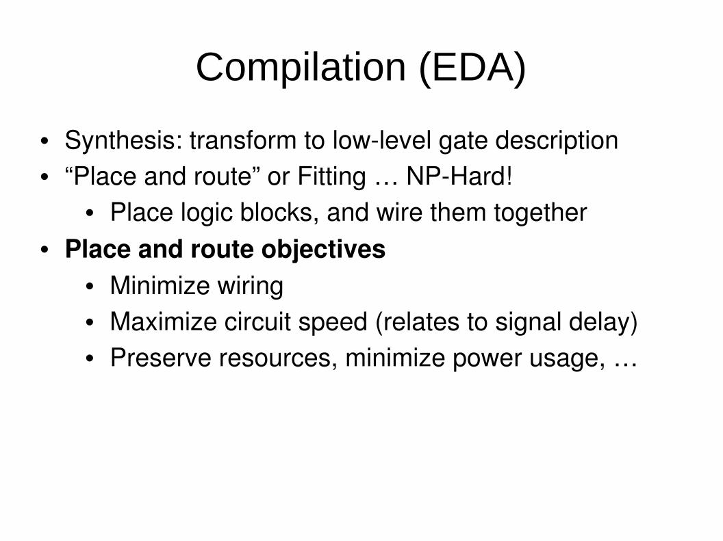
Compilation (EDA)
• Synthesis: transform to lowlevel gate description• “Place and route” or Fitting … NPHard!
• Place logic blocks, and wire them together• Place and route objectives
• Minimize wiring• Maximize circuit speed (relates to signal delay)• Preserve resources, minimize power usage, …

Place & Route – Altera

Place & Route – Xilinx

Timing
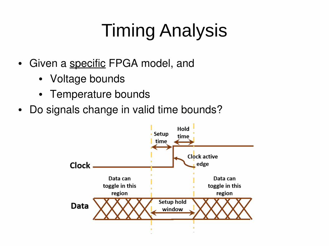
Timing Analysis
• Given a specific FPGA model, and• Voltage bounds• Temperature bounds
• Do signals change in valid time bounds?

Timing Analysis
• Pass/Fail• May fail if
• Signals are too far apart on chip (delays)• One subcircuit is too slow
• Often will give Fmax
• Maximum clock frequency where timing passes• Structure of design impacts Fmax
Timing Simulation
• Like functional simulation, but includes• Propagation delays• Timing effects
• Note: simulating a large design can be very slow• FPGA will actually run much faster atspeed• Sometimes better to just run it live!

Supplementing Simulations
• Can test a live design on the FPGA• SignalTap (Altera) or ChipScope (Xilinx)
– Interface to read/write values• Or selftest
– PRNG to autogenerate many inputs– Stress test– Automatically check result / error

Optimization Problem
• Many constraints and tradeoffs!• Design might not even fit on your chip• Speed / Area / Power tradeoffs
• Can compile a faster design, but area gets bigger• Bigger area uses more power• Low power designs are usually slower

Speed / Area / Power Trade-off
Pro
cess
ing
Tim
e
Area (logic blocks)low power high power

Low Power Design

Static Power
● Transistor leakage and bias● Constant / standby
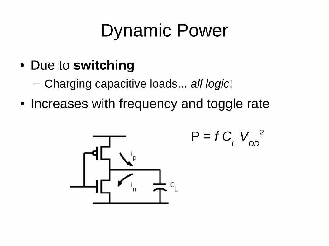
Dynamic Power
● Due to switching– Charging capacitive loads... all logic!
● Increases with frequency and toggle rate
P = f CL V
DD
2

Sources of Dynamic Power
● Anything that’s switching– Clock networks
– Logic blocks, flip-flops
– Routing wires, interconnects
– RAM, DSP blocks

Total Power
Dynamic Power Dynamic Power
● More toggling activity

Low Power Design
1.Reduce size of design
2.Try different algorithm or structure
3.Gate power-hungry circuits; clock enable (CE)
4.Use embedded (pre-built) blocks
Very good tips in:
“Quartus Power Analysis and Optimization”

1. Reduce size of design
● Less flip-flops, routing wires, etc.● Avoid redundant logic● Avoid large fan-outs and fan-ins
– Mess of wires

2. Try different algorithm/structure
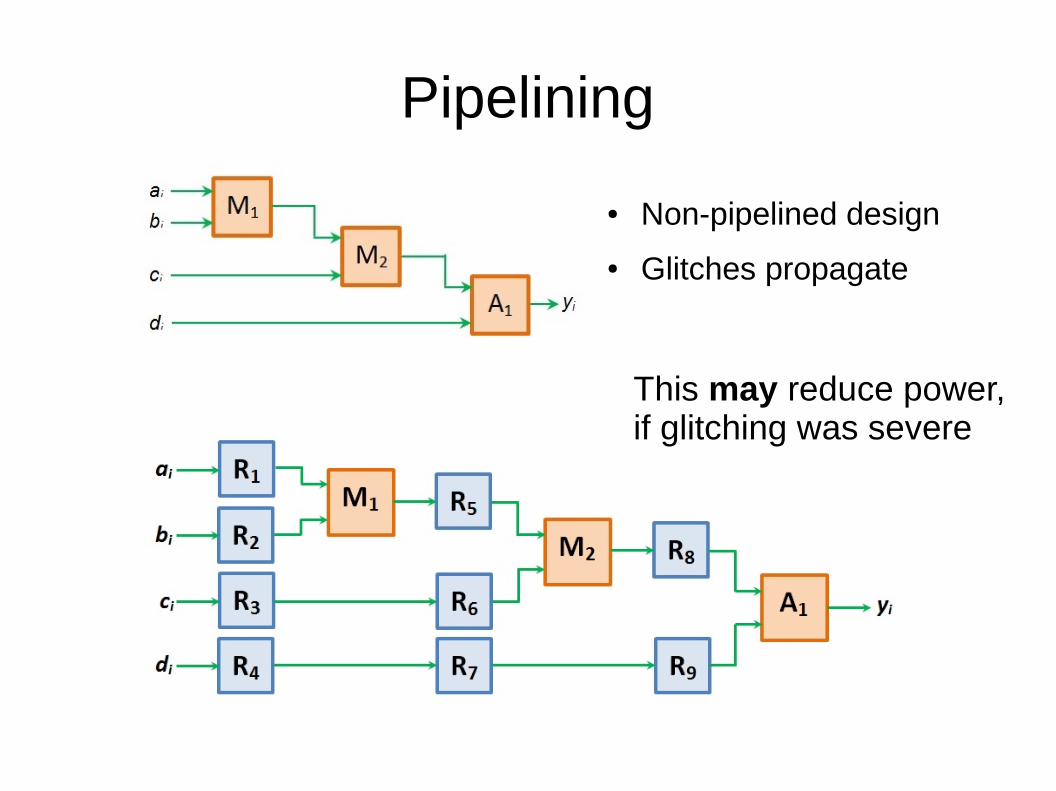
● Might restructure parts of your design● Pipelining often saves power
– Glitching problem, especially XOR

Pipelining
● Add registers
Pipelining
● Non-pipelined design
● Glitches propagate
This may reduce power, if glitching was severe

3. Gate power-hungry circuits
● Only enable parts when needed
● RAM: use clock enable, read/write enable
● Use the clock enable (CE) ports on registers
– Automatic if written a certain way
always @(posedge clk)begin if (enable) reg <= value; else reg <= reg; endend
Gate all actions on single enable signal

4. Use embedded blocks
● Many embedded blocks exist● Processors
– Try hard or soft processor, e.g. control logic
● DSP– dedicated multiplier instead of “regular logic”
altmult_accum

CAD System
● Capable of some power optimizations– If you enable in menus
● Try different pin assignments– Fitter might reduce routing interconnects
● Look at report on resource utilization

Clocks

Clock Distribution
● Clock pins bring external clock into FPGA● Clock signals are special
– Get routed onto “clock networks”
– Have buffers to support fan-out
– Symmetric wiring for low skew
– Special connectivity

Global Clock Network
● Can reach everywhere on the FPGA

Regional/Local Clock Network
● Used within a quadrant or region

Clock Network Considerations
● You must use dedicated clock pins/networks– For any resource that needs clocks
● Global clocks are the most useful– Reach everywhere
– But can use significant power● Long wires● Lots of buffers