advanced information on the nobel prize in physics 2000berger/press/phyadv.pdfadvanced information...
TRANSCRIPT

1(16)
Information Department, P.O. Box 50005, SE-104 05 Stockholm, Sweden
Phone: +46 8 673 95 00, Fax: +46 8 15 56 70, E-mail: [email protected], Web site: www.kva.se __________________________________________________________________________
Advanced information on the Nobel Prize in Physics 2000 The Royal Swedish Academy of Sciences has awarded the Nobel Prize in Physics “for basic work on information and communication technology” The prize is being awarded with one half jointly to Zhores I. Alferov, A.F. Ioffe Physico-Technical Institute, St. Petersburg, Russia, and Herbert Kroemer, University of California at Santa Barbara, California, USA, ”for developing semiconductor heterostructures used in high-speed- and opto-electronics” and one half to Jack S. Kilby, Texas Instruments, Dallas, Texas, USA ”for his part in the invention of the integrated circuit”
Information and Communication Technology Modern information and communication technology is one of the most important global technologies and has a profound influence on mankind. It is the driving force in changing the industrial society into an information and knowledge based society. Its importance can very well be compared to that of the printed book. However, its spread has been much more rapid - the full impact has occurred in tens of years rather than in hundreds of years. Only within the last decade personal computers have become common on all levels and in all environments such as homes, offices, schools, shops, factories, hospitals, etc. A striking example of the new way of information retrieval and communication is the use of Internet with the World Wide Web. Mobile telephones and high-speed fibre networks (broadband) have experienced a phenomenally rapid spread during the last few years and many more breakthroughs are expected.
2(16)
The electronic revolution has indeed transformed the world to the extent that it has lead to a new economy, the e-economy with e-business, e-auctions, e-mail, e-news, e-books, e-etc. An information system is based on hardware, software, means of communication, and system integration. It is interesting to note that the largest companies in the world, as measured by their value on the stock market, specialize in exactly these fields. It may seem difficult to identify the most important discoveries and inventions, as well as discoverers and inventors in a field which in such a short time has transformed the society and the world economy and in which enormous investments have been made. Technical progress is often made in small incremental steps and often concealed as business secrets. However, there is a general agreement that the evolution over the last few decades has been driven by the developments in the field of microelectronics. These developments in turn have been made possible through progress in many fields, most of them physics related, such as increased purity of semiconductor materials, new types of transistors with exceptional performance in high frequency and low noise level, integration of components on a single chip, semiconductor lasers, new information storage media with higher packing densities, just to mention a few of the many areas involved in microelectronics.
The role of physics With the increased performance requirements on the components, the demands on the semiconductor materials are extremely high. The purity, for example, must be of the order of a ppb (part per billion), i.e. no more deviation in identity between atoms than one individual of the population of the entire world. The number of structure defects must be extremely low. Individual layers, in a multilayer composite, must match well in crystal structure to minimize strain and the transition between layers must be abrupt on the atomic scale. The atoms in a conductor must withstand the wind of fast electrons and very thin insulating films must be without pinholes and be able to withstand high electric fields. The discovery of the transistor effect at the end of 1947 by J. Bardeen, W.H. Brattain, and W.B. Shockley (Nobel Prize 1956) is considered to be the beginning of the modern semiconductor era. It took several years to develop the transistor to a useful component. In the beginning the transistor was used as a replacement of the vacuum tube which had been developed into a highly sophisticated component during half a century. The transistor was smaller, more reliable, and dissipated less energy than the tube. Thus, the complexity of an electronic system could be increased from just a few thousands to tens of thousands of components that were soldered together on a circuit board.
3(16)
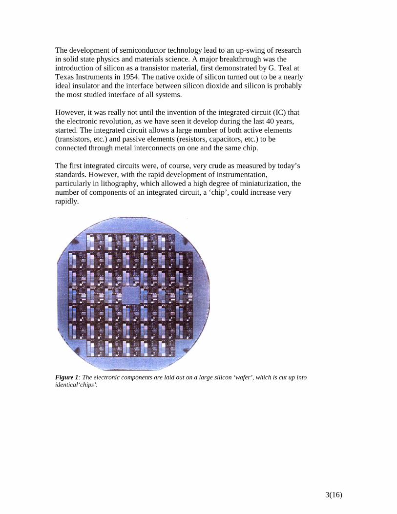
The development of semiconductor technology lead to an up-swing of research in solid state physics and materials science. A major breakthrough was the introduction of silicon as a transistor material, first demonstrated by G. Teal at Texas Instruments in 1954. The native oxide of silicon turned out to be a nearly ideal insulator and the interface between silicon dioxide and silicon is probably the most studied interface of all systems. However, it was really not until the invention of the integrated circuit (IC) that the electronic revolution, as we have seen it develop during the last 40 years, started. The integrated circuit allows a large number of both active elements (transistors, etc.) and passive elements (resistors, capacitors, etc.) to be connected through metal interconnects on one and the same chip. The first integrated circuits were, of course, very crude as measured by today’s standards. However, with the rapid development of instrumentation, particularly in lithography, which allowed a high degree of miniaturization, the number of components of an integrated circuit, a ‘chip’, could increase very rapidly.
Figure 1: The electronic components are laid out on a large silicon ‘wafer’, which is cut up into identical‘chips’.

4(16)
In the beginning of the 1960’s, shortly after the invention of the IC, Gordon Moore, one of the pioneers in Silicon Valley, formulated an empirical law stating that the performance of an IC, including the number of components on it, doubles every 18-24 months with the same chip price. This is the famous Moore’s law. Remarkably enough it is still holding up after nearly forty years, and the performance is still doubling! However, just as with the well known grains on the chessboard, the doubling will not be able to continue in this way. This has sparked the interest of physicists to suggest other types of microelectronic components.
Figure 2: Moore’s law states that the performance of microelectronics, e.g., the number of devices on a chip, doubles every 18-24 months. The evolution has so far followed this prediction very well. For the future, there are different extrapolations, depending upon assumptions on the development of process technology. Also shown in the figure is the rapid development of the size of the silicon wafers. About ten years after the invention of the IC, enough components could be connected in an integrated circuit to allow the assembly of an entire processor on a single chip. The microprocessor was invented in the early 1970’s. This new device turned out to be the working horse in a row of applications and made the development of the personal computer feasible. Just as the steam engine was the crucial machine in the industrial revolution, the personal computer became ‘the machine’ of the information and knowledge revolution. Figure 3: For further information, and photos of actual processors, see http://www.intel.com/pressroom/kits/processors/quickref.htm or http://www.ti.com

5(16)
Then computers were connected together into information networks, allowing the machines to communicate with each other. This represented the merger of two major technologies, computers and telecommunications. With increased demands on processing and transmission speeds, it was not only the number of components on a chip that was essential but also the speed of the components. This could partly be achieved by making the components smaller and smaller and less and less energy consuming. However, eventually one may have to resort to other materials and other semiconductor structures. As the ability of creating and processing information increased there was a corresponding increased need for storing information in memories and storage banks. The fast RAM (random access memory) of a computer uses transistors, where the ‘on’ and ‘off’ positions of the transistors are used to represent the binary figures 0 and 1. For mass storage of information, rotating disks are the predominant media for storage. Optical CD´s are used for read-only-memories (ROM). With the rapidly increasing needs to store gigantic amounts of data the mass storage technology has also undergone a dramatic development both in capacity and in prize reduction. The Nobel Prize in Physics of year 2000 recognizes information and communication technology as the major force in the transition from an industrial society to an information and knowledge based society. Two major physical inventions have been driving this development and have had a profound effect on the evolution of information and communication technologies as well as on the underpinning physical research: • the integrated circuit • heterostructures with implications for high frequency electronics and optoelectronics.
The integrated circuit The invention of the transistor marked the transition from the vacuum tube to a solid state component as the crucial active element in signal processing circuits. Though the transistor had many advantages compared to the vacuum tube, it was still a single component, which had to be connected to other components through cumbersome and error-causing soldering processes. The rapidly growing computer industry put increasingly harder demands on the electronics, requiring more and more circuit components. The number of transistors became the bottleneck and the limiting factor for the computer performance.

6(16)
The solution came with the integrated circuit. The concept of combining several transistors on the same piece of semiconductor crystal was prevalent in the early 1950’s and was, for example, formulated in the following way by G.W.A. Dummer at a conference in England dealing with the reliability of electronics: "With the advent of the transistor and the work in semiconductors generally, it seems now possible to envisage electronic equipment in a solid block with no connecting wires. The block may consist of layers of insulating, conducting, rectifying and amplifying materials, the electrical functions being connected directly by cutting out areas of the various layers". In retrospect it might seem as a fairly trivial task to reduce this idea to practice. However, it should be remembered that the concept was contrary to common industrial wisdom, in which the use of precious and expensive semiconductor crystal material was limited to the active components of transistors. Such material was certainly not used to fabricate elements that could be made in cheaper materials. Neither was it obvious how to handle the interconnect problem. This turned out to be a crucial question and is still a challenging task for chip designers. The progress of silicon technology during the last few decades has been astounding. One measure is the diameter of the single crystal silicon ‘boule’from which the silicon wafers are cut. The silicon industry started out with 2-inch boules. Today, there is a transfer towards 12-inch Si boules, which demands enormous investments in equipment - many billion dollars for a fabrication line.
Figure 4: A silicon ‘boule’ is a single crystal with no lattice defects.

7(16)
Jack S. Kilby – (co-)inventor of the integrated circuit Jack S. Kilby was employed by Texas Instruments in 1958. Not having earned a vacation he was left alone in the laboratory during the summer of that year. From his previous work he was interested in the question on how to handle the increased complexity following the increased number of components in a circuit. During the summer of 1958 he demonstrated that it was possible to fabricate all the different discrete components of an oscillator using only silicon as a base material and soldering them together. He continued his work along these lines and in September he showed that it was possible to fabricate a complete circuit in one piece of germanium, the prevailing semiconducting material of a fabrication line at that time. On February 6, 1959 he filed a patent application for his idea of “Miniaturized Electronic Circuits”. The mesa transistors and the passive components were connected via gold wires. In his patent application, Kilby also mentioned the possibility of using gold strip connectors “laid down on the insulating material” to electrically connect the different parts. Figure 5: For a picture of the first integrated circuit, see, e.g.: http://www.pbs.org/transistor/background1/events/icinv.html At about the same time similar developments occurred at other American laboratories. J.A. Hoerni, a Swiss scientist at Fairchild Electronics in California, showed that it was possible to use the planarization process to avoid that the mesa transistors stuck out of the surface of the semiconductor wafer, which they did in the prevalent technique and which made connections difficult. The planarization process enabled conductors to be more easily deposited on a chip of semiconducting material. Robert Noyce, at the same company, found that aluminum metal adhered very well to both silicon and silicon oxide. In his laboratory notes of January 23, 1959, he described in detail how an integrated circuit could be made in silicon using aluminum as conducting strips. His patent application dated July 30, 1959 ("Semiconductor Device-and-Lead Structure") was granted on April 25, 1961. This was considerably earlier than the grant of the Kilby patent (June 1964), despite the earlier application date of the latter. It was soon evident that the concept of the integrated circuit was going to become a commercially very important invention. Noyce and some of his colleagues formed a new company, Intel (for Integrated Electronics) with a focus on the development of the IC. The choice of interconnect material turned out to be the determining factor for the outcome of a patent conflict between Texas Instruments and Fairchild Electronics/Intel. Noyce´s choice of aluminum as "adherent to the insulating material" became the one of practical use rather than Kilby´s "gold laid down on the insulating material". In a court verdict of 1969, Fairchild was granted the
8(16)
patent right. However, the companies exchanged licenses and it may be mentioned that Fairchild never received any royalty for this patent. Kilby and Noyce are considered to be the co-inventors of the integrated circuit. Noyce became one of the founders of "Silicon Valley" and died in 1990. Kilby continued a career as an inventor. He is, for example, co-inventor of the pocket calculator, which in the beginning was considered to be of little commercial interest as the sliding rule already existed! Microelectronics has continued to evolve with the integrated circuit as the driving force. Other important inventions include the prevailing MOS-FET (Metal-Oxide-Semiconductor Field Effect Transistor) by D. Kahng and M.M. Atalla and the microprocessor by T. Hoff. Today, processors with millions of transistors are produced while random access memories with close to a billion bytes per chip are commercially available.
Heterostructures A semiconductor heterostructure may consist of two or more layers with different energy band gaps. The semiconductors of a heterostructure are either compounds, like GaAs from the III-V family (third and fifth rows of the periodic table) or semiconductor alloys like Si-Ge. Depending on the application, the value of the energy band gap of the different semiconductors is adjusted by either replacing the elements of the semiconductors (e.g. Ga by In or Al, or As by P, Sb or N) or by varying the composition of the alloy. Abrupt boundaries between different semiconductor layers are formed by several methods, such as Molecular Beam Epitaxy (MBE, developed by A.Y. Cho, J.R. Arthur and others) and Metallo-Organic Chemical Vapor Deposition (MOCVD, with H. Manasevit as an important inventor). In these methods, the layers are grown epitaxially (atomic layer by atomic layer) on a substrate with a suitable lattice constant. Heterostructures have a major impact on science and are key components in high frequency transistors and optoelectronics.

9(16)
Heterojunction transistors The current amplification in a regular bipolar junction transistor of, e.g., npn-type, is defined as the ratio between the electron and the hole currents. The electrons rapidly pass the base from the emitter to the collector without recombination. At the same time holes, that are injected into the emitter from the base, limit the current amplification. Doping the base less results in increased amplification, but at the same time in increased base resistance. Together with the emitter/base capacitance, this leads to a high RC-time constant and severely limits the operating speed of the transistor. The heterojunction bipolar transistor (HBT) differs from the regular one only with regard to the base, which consists of a semiconductor layer with a smaller energy band gap. This leads, e.g., to a lowering of the energy barrier for the electrons and thus a strong increase in the electron current. At the same time the hole current is unchanged, which can lead to a current amplification that is stronger than necessary. To reduce the amplification one may dope the base considerably higher and make it thinner, which then leads to a decrease in the base resistance and to a low RC-time constant, i.e. to a faster transistor.
Figure 6: An energy diagram of a semiconducting heterojunction showing that electrons pass the barrier while holes are reflected, or vice versa depending upon the doping and ratios of band gaps on either side of the junction. Combining two junctions, it is possible to confine charge carriers to the region of the lower bandgap as well as photons in a double heterostructure laser. The drawing is taken from a paper by H. Kroemer, Proc. IREE 51, 1782 (1963). The principle of increasing the emitter efficiency, by using a larger band gap than in the base, was mentioned by W.B. Shockley in his extensive transistor patent (filed 1948, granted 1951) and was discussed theoretically by I. Gubanov in 1951. However, the main analysis and suggestions were made by Herbert Kroemer, then at RCA, in 1957. For example, he suggested a graded energy gap in the base instead of an abrupt change at the junction and the existence of quasi-electric fields that affect electrons and holes differently.

10(16)
Figure 7: The different semiconducting layers comprising a High Electron Mobility Transistor (HEMT). The high mobility of the two-dimensional electron gas (2DEG) just below the heterojunction boundary and the short length of the gate have enabled very high frequency use of these low noise transistors. Electrons from one of the layers of a heterojunction can penetrate into the second layer to form a two dimensional sheet of electrons (2DEG, two-dimensional electron gas). As the doping impurities typically are separated from the 2DEG, its mobility can be very high. In a field effect transistor, the charge density in the 2DEG, and the current, is controlled by the potential applied to a gate that is close to the 2DEG layer. The frequency limit of such HEMT (High Electron Mobility Transistor, also called MODFET, MOdulation Doped Field Effect Transistor) structures has been pushed upwards to a present record of about 600 GHz (where gain disappears). The noise of these components is low. They were developed at the same time by groups at Bell Labs (R. Dingle et al.), in Japan (T. Mimura et al.) and in France (D. Delagebeaudeuf et al.) and are used in microwave applications such as wireless communication, space telecommunication, and radio astronomy.

11(16)
Figure 8: A High Electron Mobility Transistor (HEMT) - a scanning electron microscope picture of the 0.14 micron, mushroom shaped gate made by electron beam lithography (the shape is chosen to increase the cross section of the gate and decrease its resistance). The heterostructure and the two-dimensional electron gas layer is below the gate on the mesa part in the left part of the figure. The right part of the figure shows the completed device, which has 6 gate fingers, each 50 microns long. The actual transistor gave a record low noise temperature of 3 K when used in a 4-8 GHz amplifier. Compound semiconductors, as used in heterostructures, offer opportunities of combining microelectronic, optoelectronic, and microwave technologies. An example is a high-speed photo receiver integrating a heterojunction photon detector with high-speed electronics on the same chip.
Figure 9: The figure shows several types of heterojunction transistor applications within the microwave to millimeter wave spectrum. It was drawn in 1994 and illustrates that within the field of microelectronics, new devices often reach the market at half the time projected instead of the customary twice the time. Several of the applications are already on the market today, or will soon be. The largest (commercial) breakthrough has occurred in the mobile phone frequency range, which is of the order of 1 GHz.

12(16)
Lasers and heterostructures The 1964 Nobel Prize in Physics was awarded to Ch.H. Townes, N.G. Basov, and A.M. Prokhorov for fundamental work in the field of quantum electronics, which lead to the construction of oscillators and amplifiers based on the maser/laser principle. T.H. Maiman managed to fabricate the first (ruby) laser in 1960. R.N. Hall (1962) developed the first semiconductor laser, but the efficiency of the pn-type homojunction laser was not very large and it demanded a fairly large turn-on-current. Thus a continuous wave (CW) operation at room temperature was hampered. On the other hand heterostructure lasers can be operated in continuous mode at room temperature and are, by far, the dominant laser type. Heterojunction lasers are used in many applications such as laser printers, CD-players, and high speed fibre communication. Light emitting diodes use the same heterostructure design as laser diodes. They are produced in large volume and can be found in many products, such as car brake lights, traffic signals, and all kinds of displays. Photo detectors and solar cells, particularly for powering satellites, are other examples of optoelectronic devices that utilize heterojunctions. The principle of the double heterostructure laser was suggested in 1963 by H. Kroemer (then at Varian, Palo Alto) published in a scientific journal (Proc. IREE 51, 1782 (1963)) and, independently, in a patent application by Zh.I. Alferov and R.F. Kazarinov at the Ioffe Physico-Technical Institute, Leningrad (now St. Petersburg). The charge carriers, which are in an inverted population state, are concentrated into a thin layer with smaller band gap, sandwiched between layers of higher band gap. Practically no recombination occurs outside the active region, where the band gap variation causes "quasi-electric" forces that affect the electrons and holes. The densities of these excited charge carriers become much higher than in the doped regions. Furthermore, photons are confined to the active region with its lower bandgap and higher index of refraction. The heterostructure acts as an optical waveguide and the optical losses in the regions with the higher bandgap become negligible. Thus, both inverted carriers and photons, causing the laser effect, are concentrated to the active layer. It became possible to decrease the threshold current considerably and enable continuous operation without additional cooling. Several research groups contributed to the development of practical lasers, from the concept in 1963 to the first continuously operating lasers in 1970. A systematic development took place in Alferov´s group at the Ioffe institute. The first structures of GaAsP/GaAs were replaced by the better lattice matched AlGaAs/GaAs. A pulsed laser mode was obtained in a double heterostructure in late 1968 and the group could finally submit their report of a continuous laser at room temperature in May 1970. The exchange of information between the Soviet Union and the West was hampered during the Cold War era in the 1960´s, and there was a parallel, but independent development of heterostructures in the industrial laboratories of
13(16)
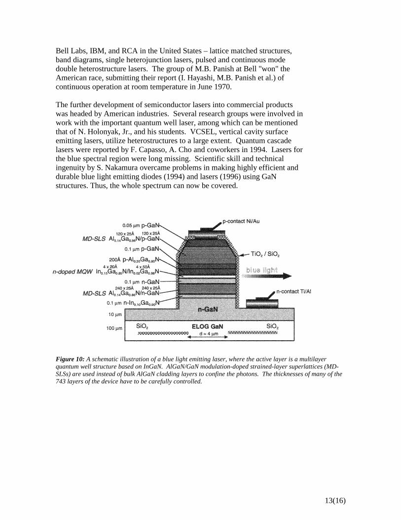
Bell Labs, IBM, and RCA in the United States – lattice matched structures, band diagrams, single heterojunction lasers, pulsed and continuous mode double heterostructure lasers. The group of M.B. Panish at Bell "won" the American race, submitting their report (I. Hayashi, M.B. Panish et al.) of continuous operation at room temperature in June 1970. The further development of semiconductor lasers into commercial products was headed by American industries. Several research groups were involved in work with the important quantum well laser, among which can be mentioned that of N. Holonyak, Jr., and his students. VCSEL, vertical cavity surface emitting lasers, utilize heterostructures to a large extent. Quantum cascade lasers were reported by F. Capasso, A. Cho and coworkers in 1994. Lasers for the blue spectral region were long missing. Scientific skill and technical ingenuity by S. Nakamura overcame problems in making highly efficient and durable blue light emitting diodes (1994) and lasers (1996) using GaN structures. Thus, the whole spectrum can now be covered.
Figure 10: A schematic illustration of a blue light emitting laser, where the active layer is a multilayer quantum well structure based on InGaN. AlGaN/GaN modulation-doped strained-layer superlattices (MD-SLSs) are used instead of bulk AlGaN cladding layers to confine the photons. The thicknesses of many of the 743 layers of the device have to be carefully controlled.

14(16)
Figure 11: A schematic representation of a Vertical Cavity Surface Emitting Laser (VCSEL) where the laser light is emitted from the surface perpendicular to the active layer (within which the photons are reflected back and forth) rather than from an edge of the layer. The thicknesses of many of the layers have to be controlled at the atomic layer level. By integrating a grating in the structure, it is possible to shape and direct the emitted beam. Hundreds of millions of edge emitting and vertical-cavity-surface emitting lasers are produced each year. Lasers for CD players dominate in number of units while lasers for communication represent the largest value.
Heterostructures in science The 2DEG formed at a selectively doped heterojunction has enabled a large amount of basic physics research. The electron transport in confined geometries is of high principal interest. Using a strong magnetic field applied perpendicular to a 2DEG, K. von Klitzing discovered the quantum Hall effect (Nobel Prize 1985) in samples supplied by M. Pepper and G. Dorda. Using even higher fields, D.C. Tsui and H.L. Stoermer (Nobel Prize 1998) discovered the fractional quantum Hall effect in ultrapure MBE material made by A.C. Gossard. Starting from a 2DEG, one can further confine the electrons to essentially one- and zero-dimensional structures. Quantized conductance in point contacts, localization, single electron tunneling, and electron structure in "artificial atoms and molecules" are fascinating phenomena.

15(16)
The band structure engineering approach (a name coined by Capasso) and using superlattices of semiconductors (heterojunctions), was pioneered by L. Esaki (Nobel Prize 1973) and his co-workers R. Tsu and L. Chang in the early 70s. It lead not only to "man made crystals" but influenced to a large extent the scientific and technical development.
The future The evolution in microelectronics has enabled the change in society caused by IT during the past decades. The present day silicon based technology has been counted out several times but it will continue to evolve for at least another decade. Physical limitations in materials will set in as atomic dimensions are approached. Maybe even more serious is that the cost of instrumentation increases very rapidly with further miniaturization. Thus, research is pursued along several lines of alternate technologies and components. But none is a clear choice presently. Speed of operation will increase. The frequency of advanced processors is presently of the order of 1 GHz (one billion of cycles per second). Research is aiming as high as one million times higher frequency (the petaflop project with 1015 operations per second). The carrier frequency of communication increases likewise; anti-collision radar, for example, is developed for the 70 GHz band. Radio astronomy needs to detect weaker signals at higher frequency. Likewise, the speed of particle detectors will increase. Wide band telecommunications will be connected to most homes in well-populated areas. Both mobile and fibre communication will increase in importance.

16(16)
Figure 12: Roadmaps have been published that try to predict the future development of microelectronics technology. Figure 13: For the latest versions of the road maps, see, for example, the one by the Semiconductor Industry Association in U.S.A. http://www.sematech.org/public/index.htm or the Nanoelectronics Roadmap by the European Union ESPRIT MEL-ARI http://www.cordis.lu/esprit/src/melna-rm.htm Microelectronics has increased its productivity (performance divided by price) about thousand-fold compared to classical technologies during the past fifteen years. One expects it to make a similar advance in the foreseeable future. The information and communication technology will continue to change society in many years to come.
Accounts of the discoveries by the inventors themselves Jack S. Kilby, Invention of the Integrated Circuit, IEEE Transactions on Electron Devices, Vol. 23, July 1976, p.648. Herbert Kroemer, Band Offsets and Chemical Bonding: The Basis for Heterostructure Applications, Physica Scripta T68, 10-16, 1996. Zh.I. Alferov, The History and Future of Semiconductor Hetrostructures from the Point of View of a Russian Scientist, Physica Scripta T68, 32-45, 1996.