advanced programming software - myscope.webs.com · solid state equipment has operational...
TRANSCRIPT

ALLEN-BRADLEY
Advanced Programming Software
(Catalog No. 1747–PA2E)
Reference Manual

Solid state equipment has operational characteristics differing from those ofelectromechanical equipment. “Safety Guidelines for the Application,Installation and Maintenance of Solid State Controls” (Publication SGI-1.1)describes some important differences between solid state equipment andhard–wired electromechanical devices. Because of this difference, and alsobecause of the wide variety of uses for solid state equipment, all personsresponsible for applying this equipment must satisfy themselves that eachintended application of this equipment is acceptable.
In no event will the Allen-Bradley Company be responsible or liable forindirect or consequential damages resulting from the use or application ofthis equipment.
The examples and diagrams in this manual are included solely for illustrativepurposes. Because of the many variables and requirements associated withany particular installation, the Allen-Bradley Company cannot assumeresponsibility or liability for actual use based on the examples and diagrams.
No patent liability is assumed by Allen-Bradley Company with respect to useof information, circuits, equipment, or software described in this manual.
Reproduction of the contents of this manual, in whole or in part, withoutwritten permission of the Allen-Bradley Company is prohibited.
Throughout this manual we use notes to make you aware of safetyconsiderations.
!ATTENTION: Identifies information about practices orcircumstances that can lead to personal injury or death, propertydamage, or economic loss.
Attentions help you:
• identify a hazard• avoid the hazard• recognize the consequences
Important: Identifies information that is especially important for successfulapplication and understanding of the product.
PLC, PLC 2, PLC 3, and PLC 5 are registered trademarks of Allen-Bradley Company, Inc.SLC and SLC 500 are trademarks of Allen-Bradley Company, Inc.IBM is a registered trademark of International Business Machines, Incorporated.
Important User Information

Important User Information 1. . . . . . . . . . . . . . . . . . . .
Preface P-1. . . . . . . . . . . . . . . . . . . . . . . . . . . . . . . . . . .
Who Should Use This Manual P-1. . . . . . . . . . . . . . . . . . . . . . .
Purpose of this Manual P-1. . . . . . . . . . . . . . . . . . . . . . . . . . . .
Contents of this Manual P-1. . . . . . . . . . . . . . . . . . . . . . . . .
Related Documentation P-3. . . . . . . . . . . . . . . . . . . . . . . . .
Common Techniques Used in this Manual P-3. . . . . . . . . . . . . .
Allen-Bradley Support P-4. . . . . . . . . . . . . . . . . . . . . . . . . . . .
Allen-Bradley Support P-4. . . . . . . . . . . . . . . . . . . . . . . . . . . .
Local Product Support P-4. . . . . . . . . . . . . . . . . . . . . . . . . .
Technical Product Assistance P-4. . . . . . . . . . . . . . . . . . . . .
Your Questions or Comments on this Manual P-4. . . . . . . . . .
The Status File 1-1. . . . . . . . . . . . . . . . . . . . . . . . . . . . . .
Status File Overview 1-1. . . . . . . . . . . . . . . . . . . . . . . . . . . . .
Conventions Used in the Displays 1-3. . . . . . . . . . . . . . . . . .
Status File Display 1-41. . . . . . . . . . . . . . . . . . . . . . . . . . . . . . .
Additional 5/03 Status File Displays 1-42. . . . . . . . . . . . . . . . .
Instruction Set Overview 2-1. . . . . . . . . . . . . . . . . . . . . .
Instruction Classifications 2-1. . . . . . . . . . . . . . . . . . . . . . . . . .
Bit Instructions - Chapter 3 2-1. . . . . . . . . . . . . . . . . . . . . .
Timer and Counter Instructions - Chapter 4 2-2. . . . . . . . . . .
Communication Instructions - Chapter 5 2-3. . . . . . . . . . . . .
I/O and Interrupt Instructions - Chapter 6 2-3. . . . . . . . . . . . .
Comparison Instructions - Chapter 7 2-4. . . . . . . . . . . . . . . .
Math Instructions - Chapter 8 2-5. . . . . . . . . . . . . . . . . . . . .
Move and Logical Instructions - Chapter 9 2-6. . . . . . . . . . . .
File Copy and File Fill Instructions - Chapter 10 2-6. . . . . . . .
Bit Shift, FIFO, and LIFO Instructions - Chapter 11 2-7. . . . . .
Sequencer Instructions - Chapter 12 2-7. . . . . . . . . . . . . . . .
Control Instructions - Chapter 13 2-8. . . . . . . . . . . . . . . . . . .
Proportional Integral Derivative Instruction - Chapter 14 2-8. .
Instruction Locator 2-9. . . . . . . . . . . . . . . . . . . . . . . . . . . . . . .
Bit Instructions 3-1. . . . . . . . . . . . . . . . . . . . . . . . . . . . .
Bit Instructions Overview 3-1. . . . . . . . . . . . . . . . . . . . . . . . . .
Examine if Closed (XIC) 3-1. . . . . . . . . . . . . . . . . . . . . . . . . . .
Examine if Open (XIO) 3-2. . . . . . . . . . . . . . . . . . . . . . . . . . . .
Output Energize (OTE) 3-2. . . . . . . . . . . . . . . . . . . . . . . . . . . .
Table of Contents
Table of Contentsii
Output Latch (OTL) 3-3. . . . . . . . . . . . . . . . . . . . . . . . . . . . . .
Output Unlatch (OTU) 3-3. . . . . . . . . . . . . . . . . . . . . . . . . . . . .
One-Shot Rising (OSR) 3-4. . . . . . . . . . . . . . . . . . . . . . . . . . .
Instruction Parameters 3-4. . . . . . . . . . . . . . . . . . . . . . . . . .
Examples 3-4. . . . . . . . . . . . . . . . . . . . . . . . . . . . . . . . .
Timer and Counter Instructions 4-1. . . . . . . . . . . . . . . . .
Using Timers and Counters 4-1. . . . . . . . . . . . . . . . . . . . . . . . .
Instruction Parameters 4-1. . . . . . . . . . . . . . . . . . . . . . . . . .
Accumulated Value (ACC) 4-1. . . . . . . . . . . . . . . . . . . . . .
Preset Value (PRE) 4-2. . . . . . . . . . . . . . . . . . . . . . . . . .
Timebase 4-2. . . . . . . . . . . . . . . . . . . . . . . . . . . . . . . . .
Timer Accuracy 4-2. . . . . . . . . . . . . . . . . . . . . . . . . . . . .
Using Timers 4-3. . . . . . . . . . . . . . . . . . . . . . . . . . . . . . . . . . .
Timer On-Delay (TON) 4-3. . . . . . . . . . . . . . . . . . . . . . . . . . . .
Status Bits 4-3. . . . . . . . . . . . . . . . . . . . . . . . . . . . . . . . . . .
Timer Off-Delay (TOF) 4-4. . . . . . . . . . . . . . . . . . . . . . . . . . . .
Status Bits 4-4. . . . . . . . . . . . . . . . . . . . . . . . . . . . . . . . . . .
Retentive Timer (RTO) 4-5. . . . . . . . . . . . . . . . . . . . . . . . . . . .
Status Bits 4-5. . . . . . . . . . . . . . . . . . . . . . . . . . . . . . . . . . .
Using Counters 4-6. . . . . . . . . . . . . . . . . . . . . . . . . . . . . . . . .
How Counters Work 4-6. . . . . . . . . . . . . . . . . . . . . . . . . . . .
Count Up (CTU) 4-7. . . . . . . . . . . . . . . . . . . . . . . . . . . . . . . . .
Status Bits 4-7. . . . . . . . . . . . . . . . . . . . . . . . . . . . . . . . . . .
Count Down (CTD) 4-8. . . . . . . . . . . . . . . . . . . . . . . . . . . . . . .
Status Bits 4-8. . . . . . . . . . . . . . . . . . . . . . . . . . . . . . . . . . .
High-Speed Counter (HSC) 4-9. . . . . . . . . . . . . . . . . . . . . . . .
Instruction Parameters 4-10. . . . . . . . . . . . . . . . . . . . . . . . . .
Application Example 4-10. . . . . . . . . . . . . . . . . . . . . . . . . .
Application Example - File 2 (Poll for DN Bit in Main Program) 4-11. . . . . . . . . . . . . .
Application Example - File 3 (Execute HSC Logic) 4-11. . . .
Reset (RES) 4-12. . . . . . . . . . . . . . . . . . . . . . . . . . . . . . . . . . .
Communication Instructions 5-1. . . . . . . . . . . . . . . . . . .
Communication Instructions Overview 5-1. . . . . . . . . . . . . . . . .
Using a 5/03 Processor 5-1. . . . . . . . . . . . . . . . . . . . . . . . .
Message Instruction (5/02 Only) 5-1. . . . . . . . . . . . . . . . . . .
Using a 5/02 Processor 5-2. . . . . . . . . . . . . . . . . . . . . . . . . . .
Related Status File Bits 5-2. . . . . . . . . . . . . . . . . . . . . . . . . .
Available Configuration Options 5-2. . . . . . . . . . . . . . . . . . . .
Entering Parameters 5-3. . . . . . . . . . . . . . . . . . . . . . . . . . .
Data Entry Screen 5-4. . . . . . . . . . . . . . . . . . . . . . . . . . . . .
Example 5-5. . . . . . . . . . . . . . . . . . . . . . . . . . . . . . . . . .
Using Status Bits 5-5. . . . . . . . . . . . . . . . . . . . . . . . . . . . . .
Table of Contents iii
Timing Diagram for a Successful 5/02 MSG Instruction 5-6. . . . .
Control Block Layout for a 5/02 Processor 5-8. . . . . . . . . . . .
Application Examples 5-9. . . . . . . . . . . . . . . . . . . . . . . . .
Example 1 5-9. . . . . . . . . . . . . . . . . . . . . . . . . . . . . . . . .
Example 2 - Program File 2 of 5/02 Processor 5-10. . . . . . .
Example 2 - Program File 2 of 5/01 Processor at Node 3 5-11
Example 3 5-12. . . . . . . . . . . . . . . . . . . . . . . . . . . . . . . . .
Using a 5/03 Processor 5-13. . . . . . . . . . . . . . . . . . . . . . . . . . .
Related Status File Bits 5-13. . . . . . . . . . . . . . . . . . . . . . . . . .
Available Configuration Options 5-14. . . . . . . . . . . . . . . . . . . .
Entering Parameters 5-14. . . . . . . . . . . . . . . . . . . . . . . . . . .
Using Status Bits 5-15. . . . . . . . . . . . . . . . . . . . . . . . . . . . . .
Local Read from a 500CPU 5-16. . . . . . . . . . . . . . . . . . . . . . . .
Monitor Display 5-17. . . . . . . . . . . . . . . . . . . . . . . . . . . . . . .
Local Read from a 485CIF 5-18. . . . . . . . . . . . . . . . . . . . . . . . .
Monitor Display 5-19. . . . . . . . . . . . . . . . . . . . . . . . . . . . . . .
Remote Read from a 500CPU 5-20. . . . . . . . . . . . . . . . . . . . . . .
Monitor Display 5-22. . . . . . . . . . . . . . . . . . . . . . . . . . . . . . .
Remote Read from a 485CIF 5-23. . . . . . . . . . . . . . . . . . . . . . . .
Monitor Display 5-24. . . . . . . . . . . . . . . . . . . . . . . . . . . . . . .
Remote Messaging 5-25. . . . . . . . . . . . . . . . . . . . . . . . . . . .
Timing Diagram for a Successful 5/03 MSG Instruction 5-26. . . . .
Control Block Layouts for a 5/03 Processor 5-29. . . . . . . . . . .
MSG Instruction Error Codes for 5/02 and 5/03 Processors 5-30
Service Communications (SVC) 5-31. . . . . . . . . . . . . . . . . . . . .
Using a 5/03 Processor 5-31. . . . . . . . . . . . . . . . . . . . . . . . .
Channel Servicing 5-32. . . . . . . . . . . . . . . . . . . . . . . . . . . . .
Application Example 5-32. . . . . . . . . . . . . . . . . . . . . . . . . .
I/O and Interrupt Instructions 6-1. . . . . . . . . . . . . . . . . . .
Additional Control Instructions 6-1. . . . . . . . . . . . . . . . . . . . . . .
Immediate Input with Mask (IIM) 6-1. . . . . . . . . . . . . . . . . . . . .
Entering Parameters 6-2. . . . . . . . . . . . . . . . . . . . . . . . . . .
Example 6-2. . . . . . . . . . . . . . . . . . . . . . . . . . . . . . . . . .
Immediate Output with Mask (IOM) 6-2. . . . . . . . . . . . . . . . . . .
Entering Parameters 6-2. . . . . . . . . . . . . . . . . . . . . . . . . . .
Example 6-2. . . . . . . . . . . . . . . . . . . . . . . . . . . . . . . . . .
I/O Event-Driven Interrupts 6-3. . . . . . . . . . . . . . . . . . . . . . . . .
I/O Interrupt Disable and Enable (IID, IIE) 6-3. . . . . . . . . . . . .
Reset Pending I/O Interrupt (RPI) 6-3. . . . . . . . . . . . . . . . . .
Entering Parameters 6-3. . . . . . . . . . . . . . . . . . . . . . . . . . .
I/O Refresh (REF) 6-4. . . . . . . . . . . . . . . . . . . . . . . . . . . . . . .
Using a 5/03 Processor 6-4. . . . . . . . . . . . . . . . . . . . . . . . .

Table of Contentsiv
Comparison Instructions 7-1. . . . . . . . . . . . . . . . . . . . . .
Comparison Instructions Overview 7-1. . . . . . . . . . . . . . . . . . . .
Indexed Word Addresses 7-1. . . . . . . . . . . . . . . . . . . . . . . .
Equal (EQU) 7-1. . . . . . . . . . . . . . . . . . . . . . . . . . . . . . . . . . .
Entering Parameters 7-1. . . . . . . . . . . . . . . . . . . . . . . . . . .
Not Equal (NEQ) 7-2. . . . . . . . . . . . . . . . . . . . . . . . . . . . . . . .
Entering Parameters 7-2. . . . . . . . . . . . . . . . . . . . . . . . . . .
Less Than (LES) 7-2. . . . . . . . . . . . . . . . . . . . . . . . . . . . . . . .
Entering Parameters 7-2. . . . . . . . . . . . . . . . . . . . . . . . . . .
Less Than or Equal (LEQ) 7-2. . . . . . . . . . . . . . . . . . . . . . . . .
Entering Parameters 7-2. . . . . . . . . . . . . . . . . . . . . . . . . . .
Greater Than (GRT) 7-2. . . . . . . . . . . . . . . . . . . . . . . . . . . . . .
Entering Parameters 7-2. . . . . . . . . . . . . . . . . . . . . . . . . . .
Greater Than or Equal (GEQ) 7-3. . . . . . . . . . . . . . . . . . . . . . .
Entering Parameters 7-3. . . . . . . . . . . . . . . . . . . . . . . . . . .
Masked Comparison for Equal (MEQ) 7-3. . . . . . . . . . . . . . . . .
Entering Parameters 7-3. . . . . . . . . . . . . . . . . . . . . . . . . . .
Limit Test (LIM) 7-3. . . . . . . . . . . . . . . . . . . . . . . . . . . . . . . . .
Entering Parameters 7-3. . . . . . . . . . . . . . . . . . . . . . . . . . .
True/False Status of the Instruction 7-4. . . . . . . . . . . . . . .
Math Instructions 8-1. . . . . . . . . . . . . . . . . . . . . . . . . . . .
Application Techniques with 5/02 Series C and later and 5/03 processors 8-1. . . . . . . . . . . . . . . . . . . . . . . . .
Math Instructions Overview 8-1. . . . . . . . . . . . . . . . . . . . . . . . .
Instruction Parameters 8-1. . . . . . . . . . . . . . . . . . . . . . . . . .
Indexed Word Addresses 8-2. . . . . . . . . . . . . . . . . . . . . . . .
Using Arithmetic Status Bits 8-2. . . . . . . . . . . . . . . . . . . . . .
Overflow Trap Bit, S:5/0 8-2. . . . . . . . . . . . . . . . . . . . . . . . .
Math Register, S:13 and S:14 8-2. . . . . . . . . . . . . . . . . . . . .
Add (ADD) 8-3. . . . . . . . . . . . . . . . . . . . . . . . . . . . . . . . . . . .
Arithmetic Status Bits 8-3. . . . . . . . . . . . . . . . . . . . . . . . . . .
Math Register 8-3. . . . . . . . . . . . . . . . . . . . . . . . . . . . . . . .
Subtract (SUB) 8-3. . . . . . . . . . . . . . . . . . . . . . . . . . . . . . . . .
Arithmetic Status Bits 8-3. . . . . . . . . . . . . . . . . . . . . . . . . . .
Math Register 8-3. . . . . . . . . . . . . . . . . . . . . . . . . . . . . . . .
32�Bit Addition and Subtraction-Series C and Later5/02 and 5/03 Processors 8-4. . . . . . . . . . . . . . . . . . . . . . .
Math Overflow Selection Bit S:2/14 8-4. . . . . . . . . . . . . . . . .
Example of 32�bit Addition 8-4. . . . . . . . . . . . . . . . . . . . . .
Multiply (MUL) 8-6. . . . . . . . . . . . . . . . . . . . . . . . . . . . . . . . . .
Arithmetic Status Bits 8-6. . . . . . . . . . . . . . . . . . . . . . . . . . .
Math Register 8-6. . . . . . . . . . . . . . . . . . . . . . . . . . . . . . . .
Table of Contents v
Divide (DIV) 8-6. . . . . . . . . . . . . . . . . . . . . . . . . . . . . . . . . . . .
Arithmetic Status Bits 8-6. . . . . . . . . . . . . . . . . . . . . . . . . . .
Math Register 8-6. . . . . . . . . . . . . . . . . . . . . . . . . . . . . . . .
Double Divide (DDV) 8-7. . . . . . . . . . . . . . . . . . . . . . . . . . . . .
Arithmetic Status Bits 8-7. . . . . . . . . . . . . . . . . . . . . . . . . . .
Math Register 8-7. . . . . . . . . . . . . . . . . . . . . . . . . . . . . . . .
Negate (NEG) 8-7. . . . . . . . . . . . . . . . . . . . . . . . . . . . . . . . . .
Arithmetic Status Bits 8-7. . . . . . . . . . . . . . . . . . . . . . . . . . .
Math Register 8-7. . . . . . . . . . . . . . . . . . . . . . . . . . . . . . . .
Clear (CLR) 8-8. . . . . . . . . . . . . . . . . . . . . . . . . . . . . . . . . . . .
Arithmetic Status Bits 8-8. . . . . . . . . . . . . . . . . . . . . . . . . . .
Math Register 8-8. . . . . . . . . . . . . . . . . . . . . . . . . . . . . . . .
Convert to BCD (TOD) 8-8. . . . . . . . . . . . . . . . . . . . . . . . . . . .
Arithmetic Status Bits 8-8. . . . . . . . . . . . . . . . . . . . . . . . . . .
Math Register (when used) 8-8. . . . . . . . . . . . . . . . . . . . . . .
Example 1 - 5/02 and 5/03 processors 8-9. . . . . . . . . . . . .
Example 2 - Fixed, 5/01, 5/02, and 5/03 processors 8-9. . .
Convert from BCD (FRD) 8-11. . . . . . . . . . . . . . . . . . . . . . . . . .
Arithmetic Status Bits 8-11. . . . . . . . . . . . . . . . . . . . . . . . . . .
Math Register (when used) 8-11. . . . . . . . . . . . . . . . . . . . . . .
Example 1 - 5/02 and 5/03 processors 8-12. . . . . . . . . . . . .
Example 2 - Fixed, 5/01, 5/02, and 5/03 Processors 8-12. . .
Decode 4 to 1 of 16 (DCD) 8-14. . . . . . . . . . . . . . . . . . . . . . . . .
Entering Parameters 8-14. . . . . . . . . . . . . . . . . . . . . . . . . . .
Arithmetic Status Bits 8-14. . . . . . . . . . . . . . . . . . . . . . . . . . .
Math Register 8-14. . . . . . . . . . . . . . . . . . . . . . . . . . . . . . . .
Square Root (SQR) 8-15. . . . . . . . . . . . . . . . . . . . . . . . . . . . . .
Arithmetic Status Bits 8-15. . . . . . . . . . . . . . . . . . . . . . . . . . .
Math Register 8-15. . . . . . . . . . . . . . . . . . . . . . . . . . . . . . . .
Scale Data (SCL) 8-15. . . . . . . . . . . . . . . . . . . . . . . . . . . . . . . .
Example 8-15. . . . . . . . . . . . . . . . . . . . . . . . . . . . . . . . . .
Entering Parameters 8-16. . . . . . . . . . . . . . . . . . . . . . . . . . .
Arithmetic Status Bits 8-16. . . . . . . . . . . . . . . . . . . . . . . . . . .
Math Register 8-16. . . . . . . . . . . . . . . . . . . . . . . . . . . . . . . .
Application Example 1 - Converting 4mA-20mA Analog Input Signal to PID Process Variable 8-17. . . . . .
Calculating the Linear Relationship 8-17. . . . . . . . . . . . . . .
Application Example 2 - Scaling an Analog Input to Control an Analog Output 8-18. . . . . . . . . . . . . . . . . . . .
Calculating the Linear Relationship 8-18. . . . . . . . . . . . . . .

Table of Contentsvi
Move and Logical Instructions 9-1. . . . . . . . . . . . . . . . . .
Move and Logical Instructions Overview 9-1. . . . . . . . . . . . . . . .
Instruction Parameters 9-1. . . . . . . . . . . . . . . . . . . . . . . . . .
Indexed Word Addresses 9-1. . . . . . . . . . . . . . . . . . . . . . . .
Arithmetic Status Bits 9-2. . . . . . . . . . . . . . . . . . . . . . . . . . .
Overflow Trap Bit, S:5/0 9-2. . . . . . . . . . . . . . . . . . . . . . . . .
Math Register, S:13 and S:14 9-2. . . . . . . . . . . . . . . . . . . . .
Move (MOV) 9-2. . . . . . . . . . . . . . . . . . . . . . . . . . . . . . . . . . .
Entering Parameters 9-2. . . . . . . . . . . . . . . . . . . . . . . . . . .
Arithmetic Status Bits 9-2. . . . . . . . . . . . . . . . . . . . . . . . . . .
Masked Move (MVM) 9-3. . . . . . . . . . . . . . . . . . . . . . . . . . . . .
Entering Parameters 9-3. . . . . . . . . . . . . . . . . . . . . . . . . . .
Arithmetic Status Bits 9-3. . . . . . . . . . . . . . . . . . . . . . . . . . .
Operation 9-3. . . . . . . . . . . . . . . . . . . . . . . . . . . . . . . . .
And (AND) 9-4. . . . . . . . . . . . . . . . . . . . . . . . . . . . . . . . . . . .
Arithmetic Status Bits 9-4. . . . . . . . . . . . . . . . . . . . . . . . . . .
Or (OR) 9-4. . . . . . . . . . . . . . . . . . . . . . . . . . . . . . . . . . . . . . .
Arithmetic Status Bits 9-4. . . . . . . . . . . . . . . . . . . . . . . . . . .
Exclusive Or (XOR) 9-5. . . . . . . . . . . . . . . . . . . . . . . . . . . . . .
Arithmetic Status Bits 9-5. . . . . . . . . . . . . . . . . . . . . . . . . . .
Not (NOT) 9-5. . . . . . . . . . . . . . . . . . . . . . . . . . . . . . . . . . . . .
Arithmetic Status Bits 9-5. . . . . . . . . . . . . . . . . . . . . . . . . . .
File Copy and File Fill Instructions 10-1. . . . . . . . . . . . . . .
File Copy and Fill Instructions Overview 10-1. . . . . . . . . . . . . . . .
Effect on the Index Register in 5/02 and 5/03 Processors 10-1. .
File Copy (COP) 10-1. . . . . . . . . . . . . . . . . . . . . . . . . . . . . . . .
Entering Parameters 10-1. . . . . . . . . . . . . . . . . . . . . . . . . . .
File Fill (FLL) 10-2. . . . . . . . . . . . . . . . . . . . . . . . . . . . . . . . . . .
Entering Parameters 10-2. . . . . . . . . . . . . . . . . . . . . . . . . . .
Bit Shift, FIFO, and LIFO Instructions 11-1. . . . . . . . . . . . .
Bit Shift, FIFO, and LIFO Instructions Overview 11-1. . . . . . . . . . .
Effect on the Index Register in 5/02 and 5/03 Processors 11-1. .
Bit Shift Left and Bit Shift Right 11-2. . . . . . . . . . . . . . . . . . . . . .
Entering Parameters 11-2. . . . . . . . . . . . . . . . . . . . . . . . . . .
Effects on Index Register S:24 11-2. . . . . . . . . . . . . . . . . . . . .
Operation - Bit Shift Left 11-3. . . . . . . . . . . . . . . . . . . . . . .
Operation - Bit Shift Right 11-3. . . . . . . . . . . . . . . . . . . . . .
FIFO Load (FFL) FIFO Unload (FFU) 11-4. . . . . . . . . . . . . . . . . .
Entering Parameters 11-4. . . . . . . . . . . . . . . . . . . . . . . . . . .
Operation 11-5. . . . . . . . . . . . . . . . . . . . . . . . . . . . . . . . .
Effects on Index Register S:24 11-6. . . . . . . . . . . . . . . . . . . . .

Table of Contents vii
LIFO Load (LFL) LIFO Unload (LFU) 11-6. . . . . . . . . . . . . . . . . .
Entering Parameters 11-6. . . . . . . . . . . . . . . . . . . . . . . . . . .
Operation 11-6. . . . . . . . . . . . . . . . . . . . . . . . . . . . . . . . .
Effects on Index Register S:24 11-7. . . . . . . . . . . . . . . . . . . . .
Sequencer Instructions 12-1. . . . . . . . . . . . . . . . . . . . . . .
Sequencer Instructions Overview 12-1. . . . . . . . . . . . . . . . . . . .
Applications Requiring More than 16-Bits 12-1. . . . . . . . . . . . .
Effect on the Index Register in 5/02 and 5/03 Processors 12-1. .
Sequencer Output (SQO) Sequencer Compare (SQC) 12-2. . . . .
Entering Parameters 12-2. . . . . . . . . . . . . . . . . . . . . . . . . . .
Operation - Sequencer Output 12-3. . . . . . . . . . . . . . . . . .
Effects on Index Register S:24 12-4. . . . . . . . . . . . . . . . . . . . .
Operation - Sequencer Compare 12-5. . . . . . . . . . . . . . . .
Effects on Index Register S:24 12-6. . . . . . . . . . . . . . . . . . . . .
Sequencer Load (SQL) 12-7. . . . . . . . . . . . . . . . . . . . . . . . . . . .
Entering Parameters 12-7. . . . . . . . . . . . . . . . . . . . . . . . . . .
Operation 12-8. . . . . . . . . . . . . . . . . . . . . . . . . . . . . . . . .
Effects on Index Register S:24 12-8. . . . . . . . . . . . . . . . . . . . .
Control Instructions 13-1. . . . . . . . . . . . . . . . . . . . . . . . . .
Jump to Label (JMP) 13-1. . . . . . . . . . . . . . . . . . . . . . . . . . . . .
Entering Parameters 13-1. . . . . . . . . . . . . . . . . . . . . . . . . . .
Label (LBL) 13-2. . . . . . . . . . . . . . . . . . . . . . . . . . . . . . . . . . . .
Entering Parameters 13-2. . . . . . . . . . . . . . . . . . . . . . . . . . .
Jump to Subroutine (JSR) 13-2. . . . . . . . . . . . . . . . . . . . . . . . . .
Nesting Subroutine Files 13-2. . . . . . . . . . . . . . . . . . . . . . . . .
Entering Parameters 13-3. . . . . . . . . . . . . . . . . . . . . . . . . . .
Subroutine (SBR) 13-3. . . . . . . . . . . . . . . . . . . . . . . . . . . . . . . .
Return from Subroutine (RET) 13-4. . . . . . . . . . . . . . . . . . . . . . .
Using 5/02 and 5/03 Processors 13-4. . . . . . . . . . . . . . . . . . .
Master Control Reset (MCR) 13-4. . . . . . . . . . . . . . . . . . . . . . . .
Temporary End (TND) 13-5. . . . . . . . . . . . . . . . . . . . . . . . . . . .
Suspend (SUS) 13-5. . . . . . . . . . . . . . . . . . . . . . . . . . . . . . . . .
Entering Parameters 13-5. . . . . . . . . . . . . . . . . . . . . . . . . . .
Selectable Timed Interrupts 13-6. . . . . . . . . . . . . . . . . . . . . . . . .
Selectable Timed Interrupt Disable and Enable (STD, STE) 13-6
Selectable Timed Interrupt Start (STS) 13-6. . . . . . . . . . . . . . .
Interrupt Subroutine (INT) 13-6. . . . . . . . . . . . . . . . . . . . . . . . . .

Table of Contentsviii
Proportional Integral Derivative Instruction 14-1. . . . . . . .
PID Overview 14-1. . . . . . . . . . . . . . . . . . . . . . . . . . . . . . . . . .
The PID Concept 14-1. . . . . . . . . . . . . . . . . . . . . . . . . . . . . . . .
The PID Equation 14-2. . . . . . . . . . . . . . . . . . . . . . . . . . . . . . . .
Entering Parameters 14-2. . . . . . . . . . . . . . . . . . . . . . . . . . .
Monitor Display Screen 14-7. . . . . . . . . . . . . . . . . . . . . . . . . .
PID Instruction Flags 14-7. . . . . . . . . . . . . . . . . . . . . . . . . . . . .
Control Block Layout 14-9. . . . . . . . . . . . . . . . . . . . . . . . . . . . .
Runtime Errors 14-10. . . . . . . . . . . . . . . . . . . . . . . . . . . . . . . . .
PID and Analog I/O Scaling 14-11. . . . . . . . . . . . . . . . . . . . . . . . .
Application Notes 14-14. . . . . . . . . . . . . . . . . . . . . . . . . . . . . . . .
Input/Output Ranges 14-14. . . . . . . . . . . . . . . . . . . . . . . . . . .
Scaling to Engineering Units 14-14. . . . . . . . . . . . . . . . . . . . . .
Zero-crossing Deadband DB 14-15. . . . . . . . . . . . . . . . . . . . .
Output Alarms 14-16. . . . . . . . . . . . . . . . . . . . . . . . . . . . . . . .
Output Limiting with Anti�reset Windup 14-16. . . . . . . . . . . . . . .
The Manual Mode 14-17. . . . . . . . . . . . . . . . . . . . . . . . . . . . .
PID Rungstate 14-17. . . . . . . . . . . . . . . . . . . . . . . . . . . . . . . .
Feed Forward or Bias 14-19. . . . . . . . . . . . . . . . . . . . . . . . . . .
Time Proportioning Outputs 14-19. . . . . . . . . . . . . . . . . . . . . . .
Example - Time proportioning outputs 14-20. . . . . . . . . . . . .
PID Tuning 14-21. . . . . . . . . . . . . . . . . . . . . . . . . . . . . . . . . .
Procedure 14-21. . . . . . . . . . . . . . . . . . . . . . . . . . . . . . . . .
Verifying the Scaling of Your Continuous System 14-23. . . . . .
Determining the Initial Loop Update Time 14-23. . . . . . . . . . .
Troubleshooting Faults 15-1. . . . . . . . . . . . . . . . . . . . . . .
Clearing Faults 15-1. . . . . . . . . . . . . . . . . . . . . . . . . . . . . . . . .
Automatically Clearing Faults 15-1. . . . . . . . . . . . . . . . . . . . .
Manually Clearing Faults 15-1. . . . . . . . . . . . . . . . . . . . . . . . .
User Fault Routine in Effect - 5/02 and 5/03 Processors Only 15-2. . . . . . . . . . . . . . . . . . . . . . . . . . . .
Status File Fault Display 15-3. . . . . . . . . . . . . . . . . . . . . . . . . . .
Troubleshooting the 5/03 Processor 15-4. . . . . . . . . . . . . . . . . . .
Powerup LED Display 15-4. . . . . . . . . . . . . . . . . . . . . . . . . . .
LED Display While Downloading an Operating System 15-4. . .
Error Code Description, Cause, and Recommended Action 15-5. .
Powerup Errors 15-5. . . . . . . . . . . . . . . . . . . . . . . . . . . . . . .
Going-to-Run Errors 15-6. . . . . . . . . . . . . . . . . . . . . . . . . . .
Runtime Errors 15-7. . . . . . . . . . . . . . . . . . . . . . . . . . . . . . .
User Program Instruction Errors 15-9. . . . . . . . . . . . . . . . . . .

Table of Contents ix
Understanding the Fault Routine - 5/02 and 5/03 Processors 16-1. . . . . . . . . . . . . . . . . .
Overview of the Fault Routine 16-1. . . . . . . . . . . . . . . . . . . . . . .
Status File Data Saved 16-1. . . . . . . . . . . . . . . . . . . . . . . . . .
Recoverable and Non- Recoverable User Faults 16-1. . . . . . . . .
Creating a Fault Routine 16-2. . . . . . . . . . . . . . . . . . . . . . . . . . .
Application Example 16-2. . . . . . . . . . . . . . . . . . . . . . . . . . . . . .
Fault Routine - Subroutine File 3 16-3. . . . . . . . . . . . . . . . .
Subroutine File 4 - Executed for Error 0020 16-4. . . . . . . . .
Subroutine File 5 - Executed for Error 0034 16-5. . . . . . . . .
Understanding the Discrete Input Interrupt -5/03 Processor Only 17-1. . . . . . . . . . . . . . . . . . . . . .
Overview of the Discrete Input Interrupt 17-1. . . . . . . . . . . . . . . .
Basic Programming Procedure for the DII Function 17-1. . . . . .
Example 17-2. . . . . . . . . . . . . . . . . . . . . . . . . . . . . . . . . .
Operation 17-2. . . . . . . . . . . . . . . . . . . . . . . . . . . . . . . . . . . . .
Counter Mode 17-2. . . . . . . . . . . . . . . . . . . . . . . . . . . . . . . .
Event Mode 17-2. . . . . . . . . . . . . . . . . . . . . . . . . . . . . . . . . .
DII Subroutine Content 17-3. . . . . . . . . . . . . . . . . . . . . . . . . .
Interrupt Latency and Interrupt Occurrences 17-3. . . . . . . . . . .
Interrupt Priorities 17-4. . . . . . . . . . . . . . . . . . . . . . . . . . . . . .
Status File Data Saved 17-4. . . . . . . . . . . . . . . . . . . . . . . . . .
Reconfigurability 17-4. . . . . . . . . . . . . . . . . . . . . . . . . . . . . .
DII Parameters 17-5. . . . . . . . . . . . . . . . . . . . . . . . . . . . . . . . .
Status File Display 17-7. . . . . . . . . . . . . . . . . . . . . . . . . . . . . . .
Additional 5/03 Status File Displays 17-8. . . . . . . . . . . . . . . . .
Application Example 17-9. . . . . . . . . . . . . . . . . . . . . . . . . . . . . .
Ladder Diagram for the Bottling Application 17-10. . . . . . . . .
Understanding Selectable Timed Interrupts - 5/02 and 5/03 Processors 18-1. . . . . . . . . . . . . . . . . .
STI Overview 18-1. . . . . . . . . . . . . . . . . . . . . . . . . . . . . . . . . . .
Basic Programming Procedure for the STI Function 18-1. . . . .
Operation 18-2. . . . . . . . . . . . . . . . . . . . . . . . . . . . . . . . . . . . .
STI Subroutine Content 18-2. . . . . . . . . . . . . . . . . . . . . . . . .
Interrupt Latency and Interrupt Occurrences 18-2. . . . . . . . . . .
Interrupt Priorities 18-3. . . . . . . . . . . . . . . . . . . . . . . . . . . . . .
Status File Data Saved 18-3. . . . . . . . . . . . . . . . . . . . . . . . . .
STI Parameters 18-4. . . . . . . . . . . . . . . . . . . . . . . . . . . . . . . . .
Word S:2 18-4. . . . . . . . . . . . . . . . . . . . . . . . . . . . . . . . . .
Word 5 18-5. . . . . . . . . . . . . . . . . . . . . . . . . . . . . . . . . . .
Word 36 18-5. . . . . . . . . . . . . . . . . . . . . . . . . . . . . . . . . .

Table of Contentsx
Status File Display 18-6. . . . . . . . . . . . . . . . . . . . . . . . . . . . . . .
STD and STE Instructions 18-7. . . . . . . . . . . . . . . . . . . . . . . . . .
Selectable Timed Disable - STD 18-7. . . . . . . . . . . . . . . . . . .
Selectable Timed Enable - STE 18-7. . . . . . . . . . . . . . . . . . .
STD/STE Zone Example 18-7. . . . . . . . . . . . . . . . . . . . . . . . .
Selectable Timed Start (STS) 18-8. . . . . . . . . . . . . . . . . . . . . . .
Understanding I/O Interrupts - 5/02 and 5/03 Processors 19-1. . . . . . . . . . . . . . . . . .
I/O Overview 19-1. . . . . . . . . . . . . . . . . . . . . . . . . . . . . . . . . . .
Basic Programming Procedure for the I/O Interrupt Function 19-1
Operation 19-2. . . . . . . . . . . . . . . . . . . . . . . . . . . . . . . . . . . . .
Interrupt Subroutine (ISR) Content 19-2. . . . . . . . . . . . . . . . . .
Interrupt Latency and Interrupt Occurrences 19-2. . . . . . . . . . .
Interrupt Priorities 19-3. . . . . . . . . . . . . . . . . . . . . . . . . . . . . .
Status File Data Saved 19-4. . . . . . . . . . . . . . . . . . . . . . . . . .
I/O Interrupt Parameters 19-5. . . . . . . . . . . . . . . . . . . . . . . . . . .
Status File Display 19-6. . . . . . . . . . . . . . . . . . . . . . . . . . . . . . .
Additional 5/03 Status File Displays 19-7. . . . . . . . . . . . . . . . .
I/O Interrupt Disable (IID) andI/O Interrupt Enable (IIE) 19-8. . . . . . . . . . . . . . . . . . . . . . . .
I/O Interrupt Disable - IID 19-8. . . . . . . . . . . . . . . . . . . . . . . .
I/O Interrupt Enable - IIE 19-8. . . . . . . . . . . . . . . . . . . . . . . . .
IID/IIE Zone Example 19-9. . . . . . . . . . . . . . . . . . . . . . . . .
Reset Pending Interrupt (RPI) 19-10. . . . . . . . . . . . . . . . . . . . . . .
Interrupt Subroutine (INT) 19-10. . . . . . . . . . . . . . . . . . . . . . . . . .
Number Systems A-1. . . . . . . . . . . . . . . . . . . . . . . . . . . .
Radices Used in APS A-1. . . . . . . . . . . . . . . . . . . . . . . . . . . . .
Example A-2. . . . . . . . . . . . . . . . . . . . . . . . . . . . . . . . . .
Binary Numbers A-2. . . . . . . . . . . . . . . . . . . . . . . . . . . . . . . . .
Positive Decimal Values A-2. . . . . . . . . . . . . . . . . . . . . . . . .
Negative Decimal Values A-3. . . . . . . . . . . . . . . . . . . . . . . .
Hexadecimal Numbers A-5. . . . . . . . . . . . . . . . . . . . . . . . . . . .
Hex Mask A-6. . . . . . . . . . . . . . . . . . . . . . . . . . . . . . . . . . . . .
APS Error Messages B-1. . . . . . . . . . . . . . . . . . . . . . . . .
General Information B-1. . . . . . . . . . . . . . . . . . . . . . . . . . . . . .
A–B
Preface
P–1
Preface
Read this preface to familiarize yourself with the rest of the manual. Itprovides information concerning:
• who should use this manual• purpose of this manual• conventions used in this manual• Allen–Bradley support
Use this manual if you are responsible for designing, installing,programming, or troubleshooting control systems that use Allen–Bradleysmall logic controllers.
You should have a basic understanding of SLC 500 products. If you do not,contact your local Allen–Bradley representative for the proper trainingbefore using this product.
We recommend reviewing The Getting Started Guide for APS, CatalogNumber 1747–NM001 before using the software.
This manual is a reference guide for the Advanced Programming Software(APS). This manual:
• provides the status file• provides the instructions used in your ladder logic programs• complements the online help available at the terminal
Contents of this Manual
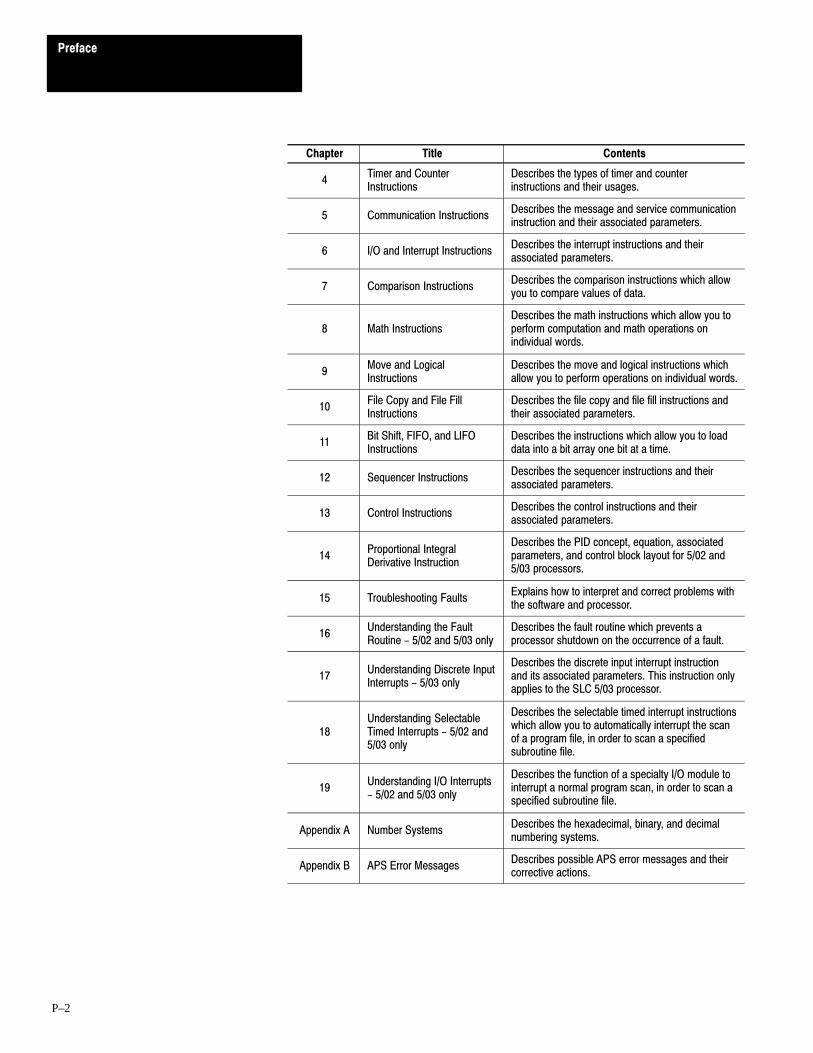
Chapter Title Contents
PrefaceDescribes the purpose, background, and scope ofthis manual. Also specifies the audience for whomthis manual is intended.
1 The Status FileDescribes major and minor faults, diagnosticinformation, processor modes, scan times, baudrates, and system node addresses.
2 Instruction Set OverviewProvides an overview of the instruction set, listingthe name, mnemonic, and function of eachinstruction.
3 Bit Instructions Describes the bit instructions and their usages.
Who Should Use This Manual
Purpose of this Manual
Preface
P–2
Chapter Title Contents
4Timer and CounterInstructions
Describes the types of timer and counterinstructions and their usages.
5 Communication InstructionsDescribes the message and service communicationinstruction and their associated parameters.
6 I/O and Interrupt InstructionsDescribes the interrupt instructions and theirassociated parameters.
7 Comparison InstructionsDescribes the comparison instructions which allowyou to compare values of data.
8 Math InstructionsDescribes the math instructions which allow you toperform computation and math operations onindividual words.
9Move and LogicalInstructions
Describes the move and logical instructions whichallow you to perform operations on individual words.
10File Copy and File FillInstructions
Describes the file copy and file fill instructions andtheir associated parameters.
11Bit Shift, FIFO, and LIFOInstructions
Describes the instructions which allow you to loaddata into a bit array one bit at a time.
12 Sequencer InstructionsDescribes the sequencer instructions and theirassociated parameters.
13 Control InstructionsDescribes the control instructions and theirassociated parameters.
14Proportional IntegralDerivative Instruction
Describes the PID concept, equation, associatedparameters, and control block layout for 5/02 and5/03 processors.
15 Troubleshooting FaultsExplains how to interpret and correct problems withthe software and processor.
16Understanding the FaultRoutine - 5/02 and 5/03 only
Describes the fault routine which prevents aprocessor shutdown on the occurrence of a fault.
17Understanding Discrete InputInterrupts - 5/03 only
Describes the discrete input interrupt instructionand its associated parameters. This instruction onlyapplies to the SLC 5/03 processor.
18Understanding SelectableTimed Interrupts - 5/02 and5/03 only
Describes the selectable timed interrupt instructionswhich allow you to automatically interrupt the scanof a program file, in order to scan a specifiedsubroutine file.
19Understanding I/O Interrupts- 5/02 and 5/03 only
Describes the function of a specialty I/O module tointerrupt a normal program scan, in order to scan aspecified subroutine file.
Appendix A Number SystemsDescribes the hexadecimal, binary, and decimalnumbering systems.
Appendix B APS Error MessagesDescribes possible APS error messages and theircorrective actions.

Preface
P–3
Related Documentation
The following documents contain additional information concerningAllen–Bradley SLC products. To obtain a copy, contact your localAllen–Bradley office or distributor.
For Read this DocumentDocumentNumber
An overview of the SLC 500 family of products SLC 500 System Overview 1747-2.30
An introduction to APS for first-time users, containing basic concepts butfocusing on simple tasks and exercises, and allowing the reader to beginprogramming in the shortest time possible
Getting Started Guide for APS 1747-NM001
A procedural manual for technical personnel who use APS to developcontrol applications
Allen-Bradley Advanced Programming Software (APS)User Manual
1747-NM002
A description on how to install and use your Fixed SLC 500programmable controller
Installation and Operation Manual for Fixed HardwareStyle Programmable Controllers
1747-NI001
A description on how to install and use your Modular SLC 500programmable controller
Installation and Operation Manual for Modular HardwareStyle Programmable Controllers
1747-NI002
A procedural and reference manual for technical personnel who use theAPS import/export utility to convert APS files to ASCII and converselyASCII to APS files
APS Import/Export User Manual 1747-NM006
A complete listing of current Automation Group documentation, includingordering instructions. Also indicates whether the documents areavailable on CD-ROM or in multi-languages.
Automation Group Publication Index SD499
A glossary of industrial automation terms and abbreviations Allen-Bradley Industrial Automation Glossary ICCG-7.1
The following conventions are used throughout this manual:
• Bulleted lists provide information, not procedural steps.• Numbered lists provide sequential steps or hierarchical information.• Text in this font indicates words or phrases you should type.• Italic type is used for emphasis.• Key names match the names shown and appear in bold, capital letters
within brackets (for example, [ ENTER] ). A function key icon matches
the name of the function key you should press, such as CONFIGOFFLINE
CONFIG
SAVE &EXIT
F8
.
Common Techniques Usedin this Manual

Preface
P–4
The following table summarizes the conventions used to distinguish thedifferences between the 5/03 keyswitch positions, the processor modes, andthe actual display on the APS status line.
When Referring to theKeyswitch Position
When Referring to theProcessor Mode
When Referring to theStatus Line
RUN position Run mode RUN
Run mode REM RUN
Program mode REM PROG
REMote position Test - Single Step mode REM SRG
Test - Single Scan mode REM SSN
Test - Continuous Scan mode REM CSN
PROGram position Program mode PROG
Allen–Bradley offers support services worldwide, with over 75 Sales/SupportOffices, 512 authorized Distributors and 260 authorized Systems Integratorslocated throughout the United States alone, plus Allen–Bradleyrepresentatives in every major country in the world.
Local Product Support
Contact your local Allen–Bradley representative for:
• sales and order support• product technical training• warranty support• support service agreements
Technical Product Assistance
If you need to contact Allen–Bradley for technical assistance, please reviewthe information in the Troubleshooting chapter first. Then call your localAllen–Bradley representative.
Your Questions or Comments on this Manual
If you have any suggestions for how this manual could be made more usefulto you, please send us your ideas on the enclosed reply card.
If you find a problem with this manual, please notify us of it on the enclosedPublication Problem Report.
Allen-Bradley SupportAllen-Bradley Support

1Chapter
1–1
The Status File
This chapter discusses the status file functions of the fixed, 5/01, 5/02, and5/03 processors. The 5/02 and 5/03 processors function like the fixed and5/01 processors. They also have additional functions as listed in the secondtable on the next page. The 5/03 processor has additional functions that arelisted in the third table on page 1–3.
The status file gives you information concerning the various instructions youuse in your program, and other information such as EEPROM functionality.The status file indicates minor faults, diagnostic information on major faults,processor modes, scan time, baud rate, system node addresses, and otherdata.
Important: Do not write to status file data unless the word or bit is listed asread/write in the descriptions that follow. If you intend writingto status file data, it is imperative that you first understand thefunction fully.
Status File Overview
Chapter 1
The Status File
1–2
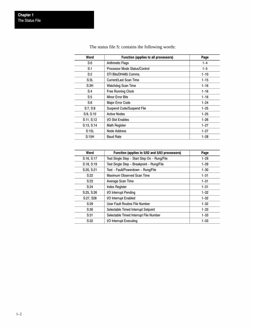
The status file S: contains the following words:
Word Function (applies to all processors) Page
S:0 Arithmetic Flags 1-4
S:1 Processor Mode Status/Control 1-5
S:2 STI Bits/DH485 Comms. 1-10
S:3L Current/Last Scan Time 1-15
S:3H Watchdog Scan Time 1-16
S:4 Free Running Clock 1-16
S:5 Minor Error Bits 1-16
S:6 Major Error Code 1-24
S:7, S:8 Suspend Code/Suspend File 1-25
S:9, S:10 Active Nodes 1-25
S:11, S;12 I/O Slot Enables 1-26
S:13, S:14 Math Register 1-27
S:15L Node Address 1-27
S:15H Baud Rate 1-28
Word Function (applies to 5/02 and 5/03 processors) Page
S:16, S:17 Test Single Step - Start Step On - Rung/File 1-29
S:18, S:19 Test Single Step - Breakpoint - Rung/File 1-29
S:20, S:21 Test - Fault/Powerdown - Rung/File 1-30
S:22 Maximum Observed Scan Time 1-31
S:23 Average Scan Time 1-31
S:24 Index Register 1-31
S:25, S:26 I/O Interrupt Pending 1-32
S:27, S28 I/O Interrupt Enabled 1-32
S:29 User Fault Routine File Number 1-32
S:30 Selectable Timed Interrupt Setpoint 1-33
S:31 Selectable Timed Interrupt File Number 1-33
S:32 I/O Interrupt Executing 1-33

Chapter 1
The Status File
1–3
Word Function (applies to a 5/03 processor only) Page
S:33 Extended Processor Status and Control Word 1-33
S:34 Reserved 1-36
S:35 Last 1 ms Scan Time 1-37
S:36 Extended Minor Error Bits 1-37
S:37 Clock/Calendar Year 1-37
S:38 Clock/Calendar Month 1-37
S:39 Clock/Calendar Day 1-37
S:40 Clock/Calendar Hours 1-38
S:41 Clock/Calendar Minutes 1-38
S:42 Clock/Calendar Seconds 1-38
S:43 to S:45 Reserved 1-38
S:46 Discrete Input Interrupt - FIle Number 1-38
S:47 Discrete Input Interrupt - Slot Number 1-38
S:48 Discrete Input Interrupt - Bit Mask 1-38
S:49 Discrete Input Interrupt - Compare Value 1-39
S:50 Discrete Input Interrupt - Preset 1-39
S:51 Discrete Input Interrupt - Return Mask 1-39
S:52 Discrete Input Interrupt - Accumulator 1-39
S:53 and S:54 Reserved 1-39
S:55 Last DII Scan Time 1-39
S:56 Maximum Observed DII Scan Time 1-40
S:57 Operating System Catalog Number 1-40
S:58 Operating System Series 1-40
S:59 Operating System FRN 1-40
S:60 Processor Catalog Number 1-40
S:61 Processor Series 1-40
S:62 Processor Revision 1-40
S:63 User Program Type 1-40
S:64 User Program Functionality Index 1-40
S:65 User RAM Size 1-40
S:66 Flash EEPROM Size 1-40
S:67 to S:83 Channel 0 Active Nodes 1-40
Conventions Used in the Displays
The following tables describe the status file functions, beginning at addressS:0 and ending at address S:83. A bullet (•) indicates that the functionapplies to the specified processor.

Chapter 1
The Status File
1–4
Address Description5/01,Fixed
5/02 5/03
S:0 Arithmetic Flags
Read/write. The arithmetic flags are assessed by the processorfollowing the execution of any math, logical, or move instruction. Thestate of these bits remains in effect until the next math, logical, ormove instruction in the program is executed.
• • •
S:0/0 Carry Bit
This bit is set by the processor if a mathematical carry or borrow isgenerated. Otherwise the bit remains cleared. This bit is assessed asif a function of unsigned math.
• • •
When a STI, I/O Slot, or Fault Routine interrupts normal execution ofyour program, the original value of S:0/0 is restored when executionresumes.
• •
When a DII interrupts normal execution of your program, the originalvalue of S:0/0 is restored when execution resumes.
•
S:0/1 Overflow Bit
This bit is set by the processor when the result of a mathematicaloperation does not fit in its destination. Otherwise the bit remainscleared. Whenever this bit is set, the overflow trap bit S:5/0 is alsoset. Refer to S:5/0.
• • •
When a STI, I/O Slot, or Fault Routine interrupts normal execution ofyour program, the original value of S:0/1 is restored when executionresumes.
• •
When a DII interrupts normal execution of your program, the originalvalue of S:0/1 is restored when execution resumes.
•
S:0/2 Zero Bit
This bit is set by the processor when the result of a math, logical, ormove instruction is zero. Otherwise the bit remains cleared.
• • •
When a STI, I/O Slot, or Fault Routine interrupts normal execution ofyour program, the original value of S:0/2 is restored when executionresumes.
• •
When a DII interrupts normal execution of your program, the originalvalue of S:0/2 is restored when execution resumes.
•
S:0/3Sign Bit
This bit is set by the processor when the result of a math, logical, ormove instruction is negative. Otherwise the bit remains cleared.
• • •
When a STI, I/O Slot, or Fault Routine interrupts normal execution ofyour program, the original value of S:0/3 is restored when executionresumes.
• •
When a DII interrupts normal execution of your program, the originalvalue of S:0/3 is restored when execution resumes.
•
S:0/4 toS:0/15
Reserved • • •

Chapter 1
The Status File
1–5
Address Description5/01,Fixed
5/02 5/03
S:1/0to
S:1/4
Processor Mode/Status/Control
Read only. Bits 0-4 function as follows:
0 0000 = (0) Remote Download in progress
0 0001 = (1) Remote Program mode (the fault mode existswhen bit S:1/13 is set along with mode 0 0001)
0 0011 = (3) Remote Suspend Idle (operation halted by SUSinstruction execution) fault mode exists when bitS:1/13 is set along with mode 0 0011
0 0110 = (6) Remote Run mode
0 0111 = (7) Remote Test continuous mode
0 1000 = (8) Remote Test single scan mode
• • •
0 1001 = (9) Remote Test single step (step until)
Note: All modes in the fixed, 5/01, and 5/02 processors areconsidered as remote because they do not have a keyswitch.
• • •
1 0000 = (16) Download in progress (keyswitch=PROGram)
1 0001 = (17) PROGram mode - the fault mode exists when bitS:1/13 is set along with mode 1 0001
1 1011 = (27) Suspend Idle - the fault mode exists when bitS:1/13 is set along with mode 1 1011(keyswitch=RUN)
1 1110 = (30) RUN - the fault mode exists when bit S:1/13 is setalong with mode 1 1110
All other values for bits 0-4 are reserved.
•
S:1/5 Forces Enabled Bit
Read only. This bit is set by the processor if you have enabled forcesin a ladder program. Otherwise, the bit remains cleared. Theprocessor Forced I/O LED is on continuously when forces areenabled.
• • •
S:1/6 Forces Installed Bit
Read only. This bit is set by the processor if you have installed forcesin a ladder program. The forces may or may not be enabled.Otherwise the bit remains cleared. The processor Forced I/O LEDflashes when forces are installed, but not enabled.
• • •
S:1/7 Communications Active Bit (Channel 1 for 5/03)
Read only. This bit is set by the processor when at least one othernode is present on the DH-485 link. Otherwise, the bit remainscleared. When you are active, you are a recognized participant in aDH-485 token�passing network.
• • •
S:1/8 Fault Override at Powerup Bit
Read/write. When set, this bit causes the processor to clear theMajor Error Halted bit S:1/13 and Minor error bits S:5/0 to S:5/7 onpower up; if the processor had previously been in the REM Run modeand had faulted. The processor then attempts to enter the REM Runmode. When this bit remains cleared (default value), the processorremains in a major fault state at power up. To program this feature,set this bit using the Data Monitor function.
• • •

Chapter 1
The Status File
1–6
Address Description5/01,Fixed
5/02 5/03
S:1/9 Startup Protection Fault Bit
Read/write. When this bit is set and power is cycled while theprocessor is in the REM Run mode, the processor executes your faultroutine prior to the execution of the first scan of your program. Youthen have the option of clearing the Major Error Halted bit S:1/13 toresume operation in the REM Run mode. If your fault routine does notreset bit S:1/13, the fault mode results.
To program this feature, use the Data Monitor function, then programyour fault routine logic accordingly. When executing the startupprotection fault routine, S:6 (major error fault code) will contain thevalue 0016H.
• •
S:1/10 Load Memory Module on Memory Error Bit
Read/ write. You can use this bit to transfer a memory moduleprogram to the processor in the event that a processor memory erroris detected at power up. A memory error means the processor cannotrun the program in the RAM because the program has beencorrupted, as detected by a parity or checksum error. This type oferror is caused by battery or capacitor drain, noise, or a powerproblem.
You must set S:1/10 in the status file of the program in the memorymodule. When a memory module is installed that has bit S:1/10 set, aprocessor memory error detected at power up causes the memorymodule program to be transferred to the processor, and the REM Runmode to be entered.
When S:1/10 is cleared in the memory module, the processorremains in a major fault condition if a memory error is detected onpower up, regardless if a memory module exists.
When S:1/10 is set in the status file of the user program in RAMmemory, the memory module must be installed at all times to enterthe REM Run or REM Test modes.
To program this feature, set this bit using the Data Monitor function.Then store the program in the memory module.
• • •

Chapter 1
The Status File
1–7
Address Description5/01,Fixed
5/02 5/03
S:1/11 Load Memory Module Always Bit
Not applicable to Series A fixed and 5/01 processors.
Read/write. When this bit is set, you can overwrite a processorprogram with a memory module program by cycling processorpower. A programming device is not required. The processormode after powerup is as follows for a 5/02 and a 5/03 processor:
REM Test/ProgramREM Run
Fault after REM Test/ProgramFault after REM Run
REM IdleREM Download
REM ProgramREM Run
REM ProgramREM Run
REM ProgramREM Program
Mode afterPowerup
Mode beforePowerdown
RunProgram
IdleFault after Run
Fault after Program
RUNPROGram
RUNRUN
PROGram
Mode after Powerup(same keyswitch position)
Mode beforePowerdown
• •
•
Note: All modes in the fixed, 5/01, and 5/02 processors areconsidered to be remote because they do not have a keyswitch.
The memory module you install in the processor must have status filebit S:1/11 set. Loading takes place if the master password and/orpassword in the processor and memory module match. Loading canalso take place if the processor has neither a password nor masterpassword.
When S:1/11 is also set in the status file of the user program in RAM,the memory module must be installed at all times to enter the REMRun or REM Test modes.
ATTENTION: The overwriting process, includingdata tables, is repeated each time you cycle power.!
To program this feature, set this bit using the Data Monitorfunction. Then store the program in the memory module.
• • •
You may choose not to overwrite data files on a per file basis. Seechapter 10 in the Advanced Programming Software User Manual,Catalog Number 1747-NM002.
•
Chapter 1
The Status File
1–8
Address Description5/01,Fixed
5/02 5/03
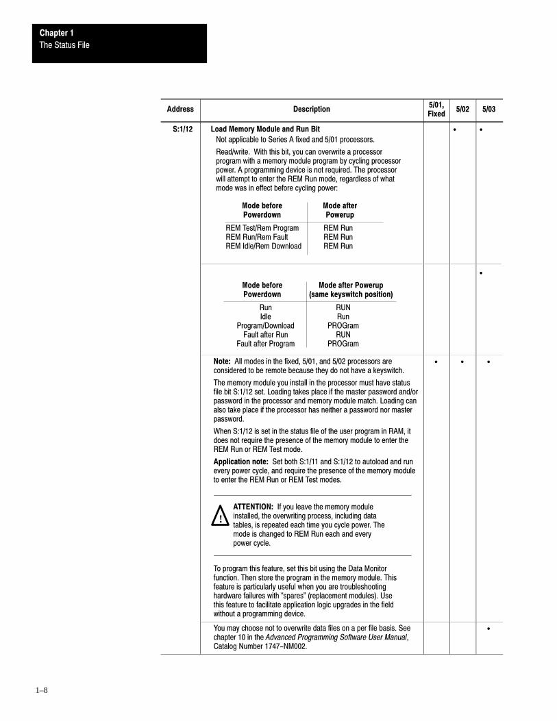
S:1/12 Load Memory Module and Run Bit
Not applicable to Series A fixed and 5/01 processors.
Read/write. With this bit, you can overwrite a processorprogram with a memory module program by cycling processorpower. A programming device is not required. The processorwill attempt to enter the REM Run mode, regardless of whatmode was in effect before cycling power:
REM Test/Rem ProgramREM Run/Rem FaultREM Idle/Rem Download
REM RunREM RunREM Run
Mode afterPowerup
Mode beforePowerdown
RunIdle
Program/DownloadFault after Run
Fault after Program
RUNRun
PROGramRUN
PROGram
Mode after Powerup(same keyswitch position)
Mode beforePowerdown
• •
•
Note: All modes in the fixed, 5/01, and 5/02 processors areconsidered to be remote because they do not have a keyswitch.
The memory module you install in the processor must have statusfile bit S:1/12 set. Loading takes place if the master password and/orpassword in the processor and memory module match. Loading canalso take place if the processor has neither a password nor masterpassword.
When S:1/12 is set in the status file of the user program in RAM, itdoes not require the presence of the memory module to enter theREM Run or REM Test mode.
Application note: Set both S:1/11 and S:1/12 to autoload and runevery power cycle, and require the presence of the memory moduleto enter the REM Run or REM Test modes.
ATTENTION: If you leave the memory moduleinstalled, the overwriting process, including datatables, is repeated each time you cycle power. Themode is changed to REM Run each and everypower cycle.
!
To program this feature, set this bit using the Data Monitorfunction. Then store the program in the memory module. Thisfeature is particularly useful when you are troubleshootinghardware failures with �spares" (replacement modules). Usethis feature to facilitate application logic upgrades in the fieldwithout a programming device.
• • •
You may choose not to overwrite data files on a per file basis. Seechapter 10 in the Advanced Programming Software User Manual,Catalog Number 1747-NM002.
•

Chapter 1
The Status File
1–9
Address Description5/01,Fixed
5/02 5/03
S:1/13 Major Error Halted Bit
Read/write. This bit is set by the processor any time a major error isencountered. The processor enters a fault condition. Word S:6, FaultCode will contain a code which can be used to diagnose the faultcondition. Any time bit S:1/13 is set, the processor:
• either places all outputs in a safe state and energizes the fault LED, or
• • •
• enters the user fault routine with outputs active, allowing the fault routine ladder logic to attempt recovery from the fault condition. If your fault routine determines that recovery is required, clear S:1/13 using ladder logic prior to exiting the fault routine. If the fault routine ladder logic does not understand the fault code, or if the routine determines that it is not desirable to continue operation, exit the fault routine with bit S:1/13 set. The outputs willbe placed in a safe state and the fault LED will be energized.
• •
When you clear bit S:1/13 using a programming device, the processormode changes from fault to either Remote Program, or Remote IdleSuspend depending on the previous mode of the processor. You canmove a value to S:6, then set S:1/13 in your ladder program togenerate an application specific Major Error.
Important: Once a major fault state exists, you must correct thecondition causing the fault, and you must also clear this bit in orderfor the processor to accept a mode change attempt (into REMProgram, REM Run, or REM Test). Also, clear S:6 to avoid theconfusion of having an error code but no fault condition.
Important: Do not re-use error codes that are defined in the SLCerror code list in chapter 15 as application specific error codes.Instead, create your own unique codes. This prevents you fromconfusing application errors with system errors. We recommend usingerror codes FFOO to FFOF to indicate application specific majorerrors.
• • •
When you clear bit S:1/13 using a programming device, the processormode changes from fault to either Program, Run, or Idle Suspenddepending on the previous mode of the processor. You can move avalue to S:6, then set S:1/13 in your ladder program to generate anapplication specific major error.
You can clear faults S:1/13 and S:6 by cycling the keyswitch toPROGram and then to RUN.
ATTENTION: If you clear this bit with the keyswitchin RUN, the processor immediately enters the RUNmode.
!
•

Chapter 1
The Status File
1–10
Address Description5/01,Fixed
5/02 5/03
S:1/14 Access Denied Bit
Read/write. You can allow or deny future access to a processor file.Set this bit to deny access. This indicates that a programming devicemust have a matching copy of the processor file in its memory inorder to monitor the ladder program. A programming device that doesnot have a matching copy of the processor file is denied access.
To program this feature, select �Future Access Disallow" when savingyour program. To provide protection from inadvertent data monitoralteration of your selection, program an unconditional OTL instructionat address S:1/14, to deny future access. Program an unconditionalOTU instruction at address S:1/14 to allow future access.
When this bit is cleared, it indicates that any compatible programmingdevice can access the ladder program (provided that passwordconditions are satisfied).
When access is denied, the programming device (APS or HHT) maynot display the ladder diagram or allow access to the Data Monitorfunction unless the device contains a matching copy of the processorfile. Functions such as change mode, clear memory, restore program,and transfer memory module are allowed regardless of this selection.A device such as the DTAM is not affected by this function.
• • •
S:1/15 First Pass Bit
Read/write. Use this bit to initialize your program as the applicationrequires. When this bit is set by the processor, it indicates that the firstscan of the user program is in progress (following power up in theRUN mode or entry into a REM Run or REM Test mode). Theprocessor clears this bit following the first scan.
When this bit is cleared, it indicates that the program is not in the firstscan of a REM Test or REM Run mode.
• • •
This bit is set during execution of the startup protection fault routine.Refer to S:1/9 for more information.
• •
S:2/0 STI (Selectable Timed Interrupt) Pending Bit
Read only. When set, this bit indicates that the STI timer has timedout and the STI routine is waiting to be executed. This bit is clearedupon starting of the STI routine, power up, exit of the REM Runmode, or execution of a true STS instruction.
• •
The STI pending bit will not be set if the STI timer expires whileexecuting the fault routine.
•
This bit is set if the STI timer expires while executing the DIIsubroutine or fault routine.
•
S:2/1 STI (Selectable Timed Interrupt) Enabled Bit
Read only. This bit is set in its default condition, or when set by theSTE or STS instruction. If set, it allows execution of the STI if the STIfile (word 31) and STI rate (word 30) are non-zero. If clear, when aninterrupt occurs, the STI subroutine does not execute and the STIPending bit is set. The STI Timer continues to run when disabled. TheSTD instruction clears this bit.
• •
Read/Write. To program this feature, use either the Data Monitorfunction to set, clear, or address this bit with your ladder logicprogram. This bit is set in its default condition, or when set by the STEor STS instruction. If set, it allows execution of the STI if the STI file(word 31) and STI rate (word 30) are non-zero. If clear, the STIsubroutine does not execute and the STI Pending bit is set. The STITimer continues to run. The STD instruction clears this bit.
•

Chapter 1
The Status File
1–11
Address Description5/01,Fixed
5/02 5/03
S:2/2 STI (Selectable Timed Interrupt) Executing Bit
Read only. When set, this bit indicates that the STI timer has timedout and the STI subroutine is currently being executed. This bit iscleared upon completion of the STI routine, powerup, or REM Runmode entry.
Application example: You can examine this bit in your fault routineto determine if your STI was executing when the fault occurred.
• •
S:2/3 Index Addressing File Range Bit
Read only. When clear, the index register can only index within thesame data file of the specified base address. When set, the indexregister can index anywhere from data file B3:0 to the end of the lastdeclared data file. This bit is selected at the time you save yourprogram.
• •
The 5/03 processor allows you to index from 0:0 to the last data file. •S:2/4 Saved with Single Step Test Enabled Bit
Read only. When clear, the Single Step Test mode function is notavailable. Clear also indicates that debug registers S:16 through S:21are inoperative. When set, the program can operate in the SingleStep Test mode. See descriptions of S:16 through S:21. When set,your program requires 0.375 instruction words (3 bytes) per rung ofadditional memory. This bit is selected at the time you save yourprogram.
• •
Note: This bit is not applicable to the 5/03 since its functionality isalways available and requires no special compile time selection.
•
S:2/5 DH-485 Incoming Command Pending Bit (Channel 1 for 5/03)
Read only. This bit is set when the processor determines that anothernode on the DH-485 network has requested information or supplied acommand to it. This bit can be set at any time. This bit is clearedwhen the processor services the request (or command).
Use this bit as a condition of an SVC instruction to enhance thecommunication capability of your processor.
• •
S:2/6 DH-485 Message Reply Pending Bit (Channel 1 for 5/03)
Read only. This bit is set when another node on the DH-485 networkhas supplied the information you requested in the MSG instruction ofyour processor. This bit is cleared when the processor stores theinformation and updates your MSG instruction.
Use this bit as a condition of an SVC instruction to enhance thecommunication capability of your processor.
• •

Chapter 1
The Status File
1–12
Address Description5/01,Fixed
5/02 5/03
S:2/7 DH-485 Outgoing Message Command Pending Bit(Channel 1 for 5/03)
Read only. This bit is set when one or more messages in yourprogram are enabled and waiting, but no message is beingtransmitted at the time. As soon as transmission of a messagebegins, the bit is cleared. After transmission, the bit is set again ifthere are further messages waiting. It remains cleared if there are nofurther messages waiting.
Use this bit as a condition of an SVC instruction to enhance thecommunication capability of your processor.
• •
S:2/8 CIF (Common Interface File) Addressing Mode
Applies to Series C and later 5/02, and 5/03 processors.
Read/write. This bit controls the mode used by the 5/02 and 5/03processor to address elements in the CIF file (data file 9) whenprocessing a communication request.
Word address mode - in effect when the bit is clear (0): This is thedefault setting, compatible with other SLC 500 devices on theDH-485 network.
Byte address mode - in effect when the bit is set (1): This mode isused when a 5/02 or 5/03 processor is receiving a message from adevice on the network, possibly through a bridge or gateway. Thissetting is compatible with Allen�Bradley PLC inter�processorcommunication.
• •
S:2/9 Memory Module Program Compare
Read only. When this bit is set inside a valid program that iscontained in a memory module, no modification of the NVRAM userprogram files is allowed. This includes online editing, programdownloading, and clear memory commands. Use this feature toprevent a programming device from altering the NVRAM programfrom the program contained in the Memory Module. If a memorymodule is installed with this bit set, and a different NVRAM userprogram is contained in NVRAM, the processor will not enter the Runmode. You must transfer the memory module program to NVRAM inorder to enter the Run mode.
•
S:2/10 STI Resolution Selection (1 ms or 10 ms) Bit
Read/write. This bit is cleared by default. When clear, this bit uses a10 ms timebase for the STI Setpoint (S:30) value. For example, thevalue 4 uses a 40 ms STI setpoint. When set, this bit uses a 1 mstimebase for the STI Setpoint (S:30). For example, the value 4 uses a4 ms STI setpoint. To program this feature, use the Data Monitorfunction to set, clear, or address this bit with your ladder program.
•
S:2/11 Discrete Input Interrupt Pending Bit
Read only. When set, this bit indicates that the DII accumulator(S:52) equals the DII preset (S:50) and the ladder file numberspecified by the DII file number (S:46) is waiting to be executed. It iscleared when the DII file number (S:46) begins executing, or on exitof the REM Run or REM Test mode.
•

Chapter 1
The Status File
1–13
Address Description5/01,Fixed
5/02 5/03
S:2/12 Discrete Input Interrupt Enabled Bit
Read/write. To program this feature, use the Data Monitor function toset, clear, or address this bit with your ladder program. This bit is setin its default condition. If set, it allows execution of the DII Subroutineif the DII file (S:46) is non-zero. If clear, when the interrupt occurs, theDII subroutine does not execute and the DII Pending bit is set. TheDII function continues to run anytime the DII file (S:46) is non-zero. Ifthe pending bit is set, the enable bit is examined at the next end ofscan.
•
S:2/13 Discrete Input Interrupt Executing Bit
Read only. When set, this bit indicates that the DII interrupt hasoccurred and the DII subroutine is currently being executed. This bitis cleared on completion of the DII routine, power up, or REM Runmode entry.
Application example: You can examine this bit in your fault routineto determine if your DII was executing when the fault occurred.
•
S:2/14 Math Overflow Selection Bit
Applies to Series C and later 5/02, and 5/03 processors.
Set this bit when you intend to use 32�bit addition and subtraction.When S:2/14 is set, and the result of an ADD, SUB, MUL, or DIVinstruction cannot be represented in the destination address(underflow or overflow),
• the overflow bit S:0/1 is set,• the overflow trap bit S:5/0 is set, and• the destination address contains the unsigned truncated
least significant 16 bits of the result.
The default condition of S:2/14 is reset (0). This provides the sameoperation as that of the Series B 5/02 processor. When S:2/14 isreset, and the result of an ADD, SUB, MUL, or DIV instruction cannotbe represented in the destination address (underflow or overflow),
• the overflow bit S:0/1 is set,• the overflow trap bit S:5/0 is set, and• the destination address contains 32767 if the result is
positive or - 32768 if the result is negative.
Note, the status of bit S:2/14 has no effect on the DDV instruction.Also, it has no effect on the math register content when using MULand DIV instructions.
To program this feature, use the Data Monitor function to set or clearthis bit. To provide protection from inadvertent data monitor alterationof your selection, program an unconditional OTL instruction ataddress S:2/14 to ensure the new math overflow operation. Programan unconditional OTU instruction at address S:2/14 to ensure theoriginal math overflow operation.
See chapter 8 in this manual for an application example of 32�bitsigned math.
• •
!ATTENTION: The 5/03 processor only asserts the stateof this bit at end of scan for the following instructions:ADD, SUB, and NEG.
•

Chapter 1
The Status File
1–14
Address Description5/01,Fixed
5/02 5/03
S:2/15 DH-485 Communications Servicing Selection Bit(Channel 1 for 5/03)
Read/write. When set, only one communication request/commandcan be serviced per END, TND, REF, or SVC. When clear, allserviceable incoming or outgoing communication requests/commands can be serviced per END, TND, REF, or SVC. Whenclear, your communication throughput will increase. However, yourscan time will increase if several communication requests/commandsare received in the same scan.
One communication request/command consists of either a DH-485incoming command, DH-485 message reply, or DH-485 outgoingmessage command. See S:2/5, S:2/6, and S:2/7 and S:33/7 (5/03only).
To program this feature, use the Data Monitor function to set or clearthis bit. To provide protection from inadvertent data monitor alterationof your selection, program an unconditional OTL instruction ataddress S:2/15 to ensure one request/command operation, orprogram an unconditional OTU instruction at address S:2/15 toensure multiple request/command operation. Alternately, yourprogram may change the state of this bit using ladder logic if yourapplication requires dynamic selection of this function.
Application example: Suppose you have a system consisting of a5/02 or 5/03 processor, an APS programmer, and a DTAM. Theprogram scan time for your user program is extremely long. Becauseof this, the programming device or DTAM takes an unusually longtime to update its screen. You can improve this update time byclearing S:2/15.
In a case such as this, the additional time spent by the processor toservice all communication at the end of the scan is insignificantcompared to the time it takes to complete one scan. You couldincrease communication throughput even further by using an SVCinstruction. See chapter 5 in this manual for more information.
• •
Chapter 1
The Status File
1–15
Address Description5/01,Fixed
5/02 5/03
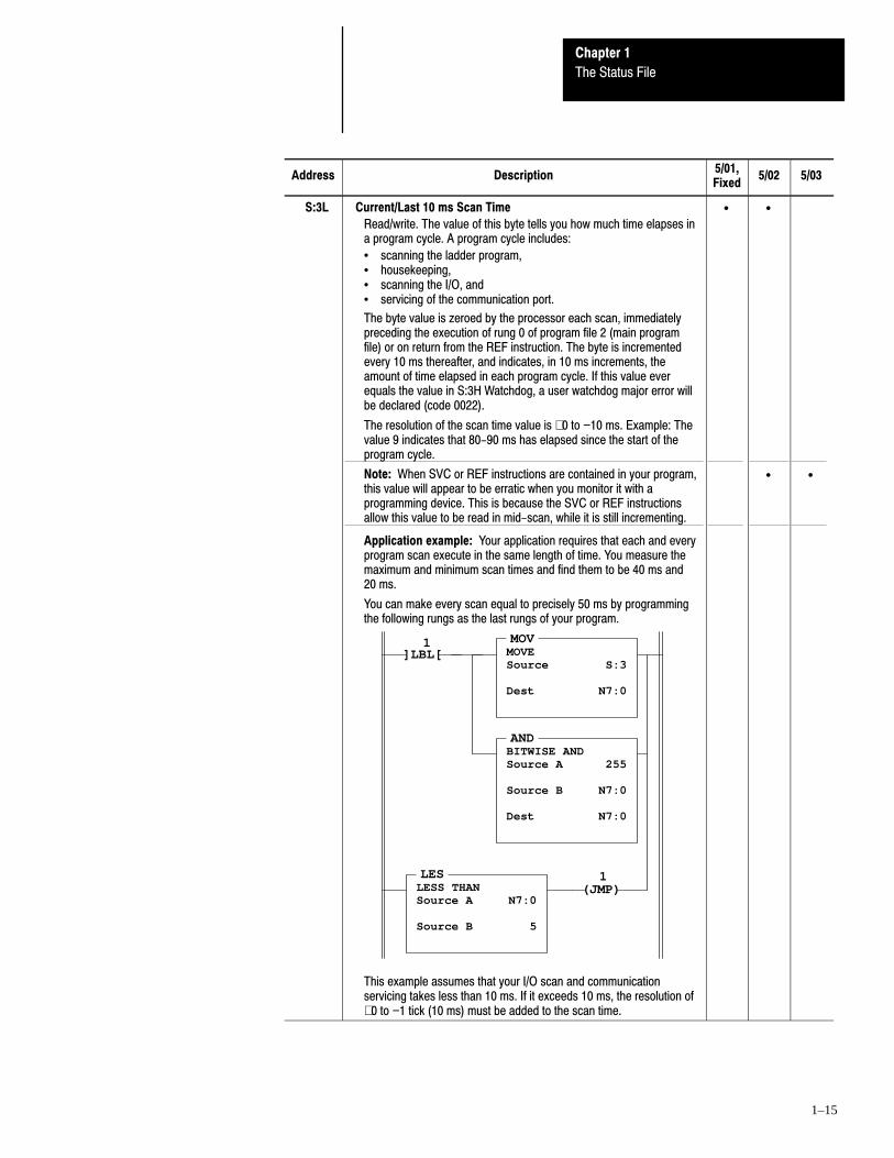
S:3L Current/Last 10 ms Scan Time
Read/write. The value of this byte tells you how much time elapses ina program cycle. A program cycle includes:
• scanning the ladder program,• housekeeping,• scanning the I/O, and• servicing of the communication port.
The byte value is zeroed by the processor each scan, immediatelypreceding the execution of rung 0 of program file 2 (main programfile) or on return from the REF instruction. The byte is incrementedevery 10 ms thereafter, and indicates, in 10 ms increments, theamount of time elapsed in each program cycle. If this value everequals the value in S:3H Watchdog, a user watchdog major error willbe declared (code 0022).
The resolution of the scan time value is +0 to −10 ms. Example: Thevalue 9 indicates that 80-90 ms has elapsed since the start of theprogram cycle.
Note: When SVC or REF instructions are contained in your program,this value will appear to be erratic when you monitor it with aprogramming device. This is because the SVC or REF instructionsallow this value to be read in mid-scan, while it is still incrementing.
Application example: Your application requires that each and everyprogram scan execute in the same length of time. You measure themaximum and minimum scan times and find them to be 40 ms and20 ms.
You can make every scan equal to precisely 50 ms by programmingthe following rungs as the last rungs of your program.
This example assumes that your I/O scan and communicationservicing takes less than 10 ms. If it exceeds 10 ms, the resolution of+0 to −1 tick (10 ms) must be added to the scan time.
]LBL[ 1
(JMP) 1LES
LESS THANSource A N7:0
Source B 5
MOVMOVESource S:3
Dest N7:0
ANDBITWISE ANDSource A 255
Source B N7:0
Dest N7:0
• •
• •
Chapter 1
The Status File
1–16
Address Description5/01,Fixed
5/02 5/03
S:3H Watchdog Scan Time Byte
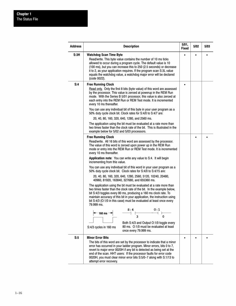
Read/write. This byte value contains the number of 10 ms ticksallowed to occur during a program cycle. The default value is 10(100 ms), but you can increase this to 250 (2.5 seconds) or decreaseit to 2, as your application requires. If the program scan S:3L valueequals the watchdog value, a watchdog major error will be declared(code 0022).
• • •
S:4 Free Running Clock
Read only. Only the first 8 bits (byte value) of this word are assessedby the processor. This value is zeroed at powerup in the REM Runmode. With the Series B 5/01 processor, this value is also zeroed ateach entry into the REM Run or REM Test mode. It is incrementedevery 10 ms thereafter.
You can use any individual bit of this byte in your user program as a50% duty cycle clock bit. Clock rates for S:4/0 to S:4/7 are:
20, 40, 80, 160, 320, 640, 1280, and 2560 ms.
The application using the bit must be evaluated at a rate more thantwo times faster than the clock rate of the bit. This is illustrated in theexample below for 5/02 and 5/03 processors.
•
Free Running Clock
Read/write. All 16 bits of this word are assessed by the processor.The value of this word is zeroed upon power up in the REM Runmode or entry into the REM Run or REM Test mode. It is incrementedevery 10 ms thereafter.
Application note: You can write any value to S:4. It will beginincrementing from this value.
You can use any individual bit of this word in your user program as a50% duty cycle clock bit. Clock rates for S:4/0 to S:4/15 are:
20, 40, 80, 160, 320, 640, 1280, 2560, 5120, 10240, 20480,40960, 81920, 163840, 327680, and 655360 ms.
The application using the bit must be evaluated at a rate more thantwo times faster than the clock rate of the bit. In the example below,bit S:4/3 toggles every 80 ms, producing a 160 ms clock rate. Tomaintain accuracy of this bit in your application, the instruction usingbit S:4/3 (O:1/0 in this case) must be evaluated at least once every79.999 ms.
160 ms
S:4/3 cycles in 160 ms
Both S:4/3 and Output O:1/0 toggle every80 ms. O:1/0 must be evaluated at leastonce every 79.999 ms.
] [S:4
3( )
O:1
0
• •
S:5 Minor Error Bits
The bits of this word are set by the processor to indicate that a minorerror has occurred in your ladder program. Minor errors, bits 0 to 7,revert to major error 0020H if any bit is detected as being set at theend of the scan. HHT users: If the processor faults for error code0020H, you must clear minor error bits S:5/0-7 along with S:1/13 toattempt error recovery.
• • •

Chapter 1
The Status File
1–17
Address Description5/01,Fixed
5/02 5/03
S:5/0 Overflow Trap Bit
Read/write. When this bit is set by the processor, it indicates that amathematical overflow has occurred in the ladder program. See S:0/1for more information.
If this bit is ever set upon execution of the END, TND, or REFinstruction, major error (0020) will be declared. To avoid this type ofmajor error from occurring, examine the state of this bit following amath instruction (ADD, SUB, MUL, DIV, DDV, NEG, SCL, TOD, orFRD), take appropriate action, and then clear bit S:5/0 using an OTUinstruction with S:5/0 or a CLR instruction with S:5.
• • •
S:5/1 Reserved • • •S:5/2 Control Register Error Bit
Read/write. The LFU, LFL, FFU, FFL, BSL, BSR, SQO, SQC, andSQL instructions are capable of generating this error. When bit S:5/2is set, it indicates that the error bit of the control instruction has beenset.
If this bit is ever set upon execution of the END, TND, or REFinstruction, major error (0020) will be declared. To avoid this type ofmajor error from occurring, examine the state of this bit following acontrol register instruction, take appropriate action, and then clear bitS:5/2 using an OTU instruction with S:5/2 or a CLR instruction withS:5.
• • •
S:5/3 Major Error Detected while Executing User Fault Routine Bit
Read/write. When set, the major error code (S:6) represents themajor error that occurred while processing the fault routine due toanother major error.
If this bit is ever set upon execution of the END, TND, or REFinstruction, major error (0020) will be declared. To avoid this type ofmajor error from occurring, examine the state of this bit inside yourfault routine, take appropriate action, and then clear bit S:5/3 using anOTU instruction with S:5/3 or a CLR instruction with S:5.
Application example: Suppose you are executing your fault routinefor fault code 0016H Startup Protection. At rung 3 inside this faultroutine, a TON containing a negative preset is executed. When rung4 is executed, fault code 0016H will be overwritten to indicate code0034H, and S:5/3 will be set.
If your fault routine did not determine that S:5/3 was set, major error0020H would be declared at the end of the first scan. To avoid thisproblem, examine S:5/3, followed by S:6, prior to returning from yourfault routine. If S:5/3 is set, take appropriate action to remedy thefault, then clear S:5/3.
• •

Chapter 1
The Status File
1–18
Address Description5/01,Fixed
5/02 5/03
S:5/4 M0-M1 Referenced on Disabled Slot Bit
Read/write. This bit is set whenever any instruction references an M0or M1 module file element for a slot that is disabled (via its I/O slotenable bit). When set, the bit indicates that an instruction could notexecute properly due to the unavailability of the addressed M0 or M1data.
If this bit is ever set upon execution of the END, TND, or REFinstruction, major error (0020) will be declared. To avoid this type ofmajor error from occurring, examine the state of this bit following aM0-M1 referenced instruction, take appropriate action, and then clearbit S:5/4 using an OTU instruction with S:5/4 or a CLR instruction withS:5.
• •
S:5/5to
S:5/7
Reserved
Read/write. Reserved for minor errors that revert to major errors atthe end of the scan.
• • •
S:5/8 Memory Module Boot Bit
Read/write. When this bit is set by the processor, it indicates that amemory module program has been transferred to the processor. Thisbit is not cleared by the processor.
Your program can examine the state of this bit on entry into the REMRun mode to determine if the memory module content has beentransferred. Word S:1/15 will be set to indicate REM Run mode entry.This information is useful when you have an application that containsretentive data and a memory module that has only bit S:1/10 set(Load Memory Module on Memory error). Use this bit to indicate thatretentive data has been lost. This bit is also helpful when using bitsS:1/11 (Load Memory Module Always) or S:1/12 (Load MemoryModule Always and Run) to distinguish a power up REM Run modeentry from a REM Program (or REM Test) mode to REM Run modeentry.
• • •
S:5/9 Memory Module Password Mismatch Bit
Read/write. This bit is set on REM Run mode entry, wheneverloading from the memory module is specified (word 1, bits 11 or 12)and the processor user program is password protected, and thememory module program does not match that password.
Use this bit to inform your application program that an autoloadingmemory module is installed but did not load due to a passwordmismatch.
• • •
S:5/10 STI (Selectable Timed Interrupt) Overflow Bit
Read/ write. This bit is set whenever the STI timer expires while theSTI routine is either executing or disabled and the pending bit isalready set.
• •
S:5/11 Battery Low Bit
Read only. This bit is set whenever the Battery Low LED is on. Thebit is cleared when the Battery Low LED is off. It is updated only inthe REM Run or REM Test modes.
• •

Chapter 1
The Status File
1–19
Address Description5/01,Fixed
5/02 5/03
S:5/12 Discrete Input Interrupt Overflow Bit
Read only. This bit is set whenever the DII interrupt occurs while stillexecuting the DII subroutine or whenever the DII interrupt occurswhile pending or disabled.
•
S:5/13 Reserved •S:5/14 Channel 0 Modem Lost
Read only. This bit is set when communication channel 0 is in theSystem mode, configured for Modem communication, and cannotcommunicate with the modem. Otherwise this bit is cleared. Themodem is considered to be lost when Carrier Detect (CD) is inactivefor more than 10 seconds or if Data Set Ready (DSR) becomesinactive. CD and DSR are pins of DF1 Channel 0. Refer to theInstallation and Operation Manual for Modular Hardware StyleProgrammable Controllers , Catalog Number 1747-NI002 for pinoutinformation.
•
S:5/15 Reserved •

Chapter 1
The Status File
1–20
Address Description5/01,Fixed
5/02 5/03
S:6 Major Error Fault Code
Read/write. A hexadecimal code is entered in this word by theprocessor when a major error is declared. Refer to S:1/13. The codedefines the type of fault, as indicated on the following pages. Thisword is not cleared by the processor.
Error codes are presented, stored, and displayed in a hexadecimalformat. Refer to appendix A for more information on the hexadecimalnumbering system.
• • •
If you enter a fault code as a parameter in an instruction in yourladder program, you must convert the code to decimal. For example,if you program an EQU instruction to go true when the error 0016occurs, enter S:6 as source A and 22, the decimal equivalent of0016H, as source B:
Application note: You can declare your own application specificmajor fault by writing a unique value to S:6 and then setting bitS:1/13.
5/02 processor users: Interrogate the value of S:6 in your faultroutine to determine the type of fault that occurred. If your programwas saved with the test single step enabled, you can also interrogateS:20 and S:21 to pinpoint the exact rung that was executing when thefault occurred.
Fault Classifications: Faults are classified as Non�User,Non�Recoverable, and Recoverable.
RecoverableUser Fault
The faultroutine mayclear the faultby clearing bitS:1/13.
Non�Recoverable User Fault
The fault routine executes for1 pass. (You may initiate aMSG instruction to anothernode to identify the faultcondition of the processor.)
Non�UserFault
The faultroutine doesnot execute.
EQUEQUALSource A S:6
Source B 22
• •
Error code descriptions and classifications are listed on pages 1-21through 1-24. Categories are:
• powerup errors• going-to-run errors• runtime errors• user program instruction errors• I/O errors
See chapter 15 of this manual for fault cause and recoveryinformation.
• • •

Chapter 1
The Status File
1–21
Fault Classification Processor
User
AddressErrorCode(Hex)
Powerup Errors Non�User Non�Recov Recov5/01,Fixed
5/02 5/03
S:6 0001 NVRAM error. X • • •
0002 Unexpected hardware watchdog timeout. X • • •
0003Memory module memory error. This error can also occur whilegoing into the REM Run mode.
X • •
0005 Reserved X •0006 Reserved X •0007 Failure during memory module transfer. X •0008 Internal software error. X •0009 Internal hardware error. X •
Fault Classification Processor
User
AddressErrorCode(Hex)
Going-to-Run Errors Non�User Non�Recov Recov5/01,Fixed
5/02 5/03
S:6 0010 The Processor does not meet the required revision level. X • • •
0011 The executable program file number 2 is absent. X • • •
0012 The ladder program has a memory error. X • • •
0013• The required memory module is absent or• S:1/10 or S:1/11 is not set as required by the program.
X • • •
0014 Internal file error. X • • •
0015 Configuration file error. X • • •
0016Startup protection after power loss. Error condition exists atpowerup when bit S:1/9 is set and powerdown occurred whilerunning.
X • •
0017 NVRAM/memory module user program mismatch. X •
0018Incompatible user program - Operating system type mismatch.This error can also occur during powerup.
X •
0019 Missing or duplicate label was detected. X •

Chapter 1
The Status File
1–22
Fault Classification Processor
User
AddressErrorCode(Hex)
Runtime Errors Non�User Non�Recov Recov5/01,Fixed
5/02 5/03
S:6 001FA program integrity problem occurred during an online editingsession.
X •
0004 Memory error occurred while in the Run mode. X •
0020A minor error bit is set at the end of the scan. Refer to S:5 minorerror bits.
X • • •
0021 Remote power failure of an expansion I/O rack occurred.
Note: A modular system that encounters an over-voltage orover-current condition in any of its power supplies can produceany of the I/O error codes listed on page 1-24 (instead of code0021). The over-voltage or over-current condition is indicatedby the power supply LED being off.
ATTENTION: Fixed and FRN 1 to 4 5/01processors - If the remote power failure occurredwhile the processor was in the REM Run mode,error 0021 will cause the major error halted bit(S:1/13) to be cleared at the next powerup of thelocal rack.
5/02 processors and FRN 5 5/01 processors -Power to the local rack does not need to be cycledto resume the REM Run mode. Once the remoterack is re-powered, the CPU will restart thesystem.
!X • • •
0022 The user watchdog scan time has been exceeded. X • • •
0023 Invalid or non�existent STI interrupt file. X • •
0024 Invalid STI interrupt interval (greater than 2550 ms or negative). X • •
0025 Excessive stack depth/JSR calls for STI routine. X • •
0026 Excessive stack depth/JSR calls for I/O interrupt routine. X • •
0027 Excessive stack depth/JSR calls for user fault routine. X • •
0028Invalid or non�existent �startup protection" fault routine filevalue.
X • •
0029
Indexed address reference outside of entire data file space(range of B3:0 through the last file).
ATTENTION: The 5/02 processor uses an index
X •
0029
!ATTENTION: The 5/02 processor uses an indexvalue of zero for the faulted instruction followingerror recovery.
X •
002AIndexed address reference is beyond specific referenced datafile.
X • •
002E Invalid DII Input slot. X •002F Invalid or non-existent DII interrupt file. X •

Chapter 1
The Status File
1–23
ERROR CODES: The characters xx in the following codesrepresent the slot number, in hex. If the exact slot cannot bedetermined, the characters xx become 1F.
RECOVERABLE I/O FAULTS (5/02 and 5/03 processorsonly): Many I/O faults are recoverable. To recover, you mustdisable the specified slot, xx, in the user fault routine. If youdo not disable slot xx, the processor will fault at the end ofthe scan.
Important: An I/O card that is severly damaged may causethe processor to indicate that an error exists in slot 1 eventhough the damaged card is installed in a slot other than 1.
Slot xx
0 001 012 02
** 3 034 045 056 067 07
Slot xx
8 089 0910 0A11 0B12 0C13 0D14 0E15 0F
Slot xx
16 1017 1118 1219 1320 1421 1522 1623 17
Slot xx
24 1825 1926 1A27 1B28 1C29 1D30 1E* 1F
SLOT NUMBERS (xx) IN HEXADECIMALI/O Errors
* This value indicates that the slot was not found (5/01, 5/02, 5/03).
** This value indicates that the slot was not found (500 fixed controller.
Fault Classification Processor
User
AddressErrorCode(Hex)
User Program Instruction Errors Non�User Non�Recov Recov5/01,Fixed
5/02 5/03
S:6 0030Attempt was made to jump to one too many nested subroutinefiles. This code can also mean that a program has potentiallyrecursive routines.
X • • •
0031 An unsupported instruction reference was detected. X • • •
0032A sequencer length/position parameter points past the end of adata file.
X • • •
0033The length of LFU, LFL, FFU, FFL, BSL, or BSR instructionpoints past the end of a data file.
X • • •
0034A negative value for a timer accumulator or preset value wasdetected.
X • • •
Fixed processors with 24 VDC inputs only: A negative or zeroHSC preset was detected in a HSC instruction.
X •
0035TND, SVC, or REF instruction is called within an interrupting oruser fault routine.
X • •
0036 An invalid value is being used for a PID instruction parameter. X • •
0038 A RET instruction was detected in a non�subroutine file. X • • •
xx50 A rack data error is detected. X • • •
xx51 A �stuck" runtime error is detected on an I/O module. X • • •
xx52A module required for the user program is detected as missingor removed.
X • • •

Chapter 1
The Status File
1–24
Fault Classification Processor
User
AddressErrorCode(Hex)
I/O Errors Non�User Non�Recov Recov5/01,Fixed
5/02 5/03
S:6 xx53When going�to�run, a user program declares a slot as unused,and that slot is detected as having an I/O module inserted. Thiscan also mean that an I/O module has reset itself.
X • • •
An attempt to enter the run or test mode was made with anempty rack.
X •
xx54A module required for the user program is detected as being thewrong type.
X • • •
xx55A discrete I/O module required for the user program is detectedas having the wrong I/O count. This code can also mean that aspecialty card driver is incorrect.
X • • •
xx56The rack configuration specified in the user program is detectedas being incorrect.
X • • •
xx57A specialty I/O module has not responded to a lock sharedmemory command within the required time limit.
X • • •
xx58A specialty I/O module has generated a generic fault. The cardfault bit is set (1) in the module's status byte.
X • • •
xx59A specialty I/O module has not responded to a command asbeing completed within the required time limit.
X • • •
xx5A Hardware interrupt problem. X • •
xx5BG file configuration error - user program G file size exceedscapacity of the module.
X • •
xx5CM0-M1 file configuration error - user program M0-M1 file sizeexceeds capacity of the module.
X • •
xx5D Interrupt service requested is not supported by the processor. X • •
xx5E Processor I/O driver (software) error. X • •xx60
toxx6F
Identifies an I/O module specific non�recoverable major error.Refer to the user manual supplied with the specialty module.
X • •
xx70to
xx7F
Identifies an I/O module specific non�recoverable major error.Refer to the user manual supplied with the specialty module.
X • •
xx90 Interrupt problem on disabled slot. X • •
xx91 A disabled slot has faulted. X • •
xx92 An invalid or non�existent module interrupt subroutine (ISR) file. X • •
xx93 Unsupported I/O module specific major error. X • •
xx94In the REM Run or REM Test mode, a module has beendetected as being inserted under power. This can also meanthat an I/O module has reset itself.
X • •
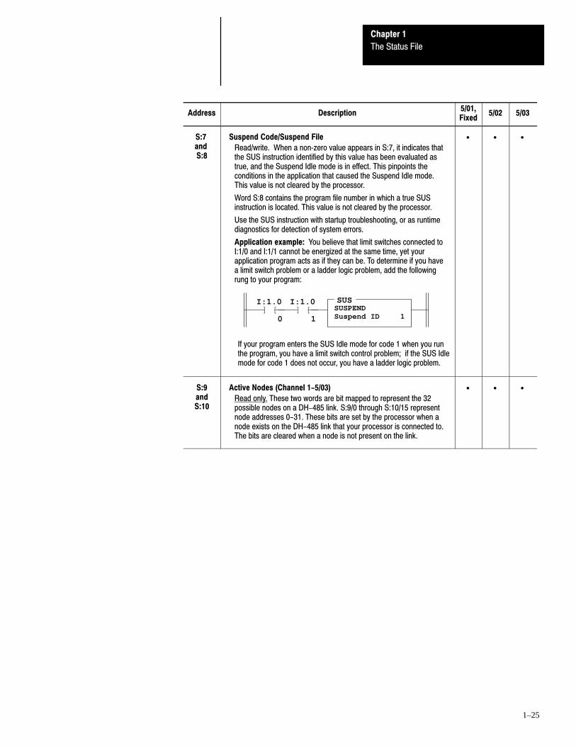
Chapter 1
The Status File
1–25
Address Description5/01,Fixed
5/02 5/03
S:7 and S:8
Suspend Code/Suspend File
Read/write. When a non�zero value appears in S:7, it indicates thatthe SUS instruction identified by this value has been evaluated astrue, and the Suspend Idle mode is in effect. This pinpoints theconditions in the application that caused the Suspend Idle mode.This value is not cleared by the processor.
Word S:8 contains the program file number in which a true SUSinstruction is located. This value is not cleared by the processor.
Use the SUS instruction with startup troubleshooting, or as runtimediagnostics for detection of system errors.
Application example: You believe that limit switches connected toI:1/0 and I:1/1 cannot be energized at the same time, yet yourapplication program acts as if they can be. To determine if you havea limit switch problem or a ladder logic problem, add the followingrung to your program:
If your program enters the SUS Idle mode for code 1 when you runthe program, you have a limit switch control problem; if the SUS Idlemode for code 1 does not occur, you have a ladder logic problem.
SUSSUSPENDSuspend ID 1
] [I:1.0
0] [
I:1.0
1
• • •
S:9 and S:10
Active Nodes (Channel 1-5/03)
Read only. These two words are bit mapped to represent the 32possible nodes on a DH-485 link. S:9/0 through S:10/15 representnode addresses 0-31. These bits are set by the processor when anode exists on the DH-485 link that your processor is connected to.The bits are cleared when a node is not present on the link.
• • •

Chapter 1
The Status File
1–26
Address Description5/01,Fixed
5/02 5/03
S:11andS:12
I/O Slot Enables
Read/write. These two words are bit mapped to represent the 30possible I/O slots in an SLC 500 system. S:11/0 represents I/O slot 0for fixed I/O systems. (Slot 0 is used for the CPU in modularsystems.) S:11/1 through S:12/14 represent I/O slots 1-30. S:12/15is unused.
When a bit is set (default condition), it allows the I/O modulecontained in the referenced slot to be updated in the I/O scan of theprocessor operating cycle.
When you clear a bit, it causes the I/O module in the referenced slotto be ignored. That is, an I/O slot enable value of 0 causes the inputimage data of an input module to freeze at its last value. Also, theoutputs of an output module will freeze at their last values, regardlessof values contained in the output image. Outputs remain frozen until:
• either power is removed,• the REM Run mode is exited, or• a major fault occurs.At that time the outputs are zeroed, until the slot is again enabled(set).
Disabled slots do not have to match the user program configuration.
ATTENTION: Make certain that you have thoroughlyexamined the effects of disabling (clearing) a slot enablebit before doing so in your application.
!
• • •
Note: The 5/02 and 5/03 processors inform each specialty I/Omodule that has been disabled/enabled. Some I/O modules mayperform other actions when disabled or re�enabled. Refer to the userinformation supplied with the specialty I/O module for possibledifferences from the above descriptions.
• •
ATTENTION: The DII instruction ignores the slotenable/disable status. Do not run the DII on a faulted slot. If youapply the DII on a disabled slot, the interrupt will occur.However, the input image will not reflect the present state of thecard.
!
This bit is applied upon detection of a DII Reconfigurebit, each DII ISR exit, and at each end of scan (END,TND, or REF).
•

Chapter 1
The Status File
1–27
Address Description5/01,Fixed
5/02 5/03
S:13andS:14
Math Register
Read/write. Use this double register to produce 32-bit signed divideand multiply operations, precision divide or double divide operations,and 5-digit BCD conversions.
These two words are used in conjunction with the MUL, DIV, DDV,FRD, and TOD math instructions. The math register value isassessed upon execution of the instruction and remains valid until thenext MUL, DIV, DDV, FRD, or TOD instruction is executed in the userprogram.
An explanation of how the math register operates is included with theinstruction definitions.
If you store 32�bit signed data values (example on page 8-4), youmust manage this data type without the aid of an assigned 32�bit datatype. For example, combine B10:0 and B10:1 to create a 32�bitsigned data value. We recommend that you keep all 32�bit signeddata in a unique data file and that you start all 32�bit values on aneven or odd word boundary for ease of application and viewing. Also,we recommend that you design, document, and view the contents of32�bit signed data in either the hexadecimal or binary radix.
• • •
When an STI, I/O Slot, or Fault Routine interrupts normal execution ofyour program, the original value of the math register is restored whenexecution resumes.
• •
When a DII interrupts normal execution of your program, the originalvalue of the math register is restored when execution resumes.
•
S:15L Node Address (Channel 1-5/03)
Read/write. This byte value contains the node address of yourprocessor on the DH-485 link. Each device on the DH-485 link musthave a unique address between the decimal values 0-31. To changea processor node address, write a value between 1-31 using eitherthe Data Monitor or node function of your programmer, then cyclepower to the processor.
The default node address of a processor is 1. The default nodeaddress of APS and the HHT programmer is 0. To provide runtimeprotection from inadvertent data monitor alteration of your selection,program this value using an unconditional MVM instruction. Use theMOV instruction in place of MVM if you also wish to protect the baudrate. The following example shows runtime protection of nodeaddress 3.
MVMMASKED MOVESource N7:100
Mask 00FF
Dest S:15
MOVMOVESource 3
Dest N7:100
• • •
When a configure channel command is received for channel 1, thenode address is overwritten with the value contained in your channelconfiguration.
•
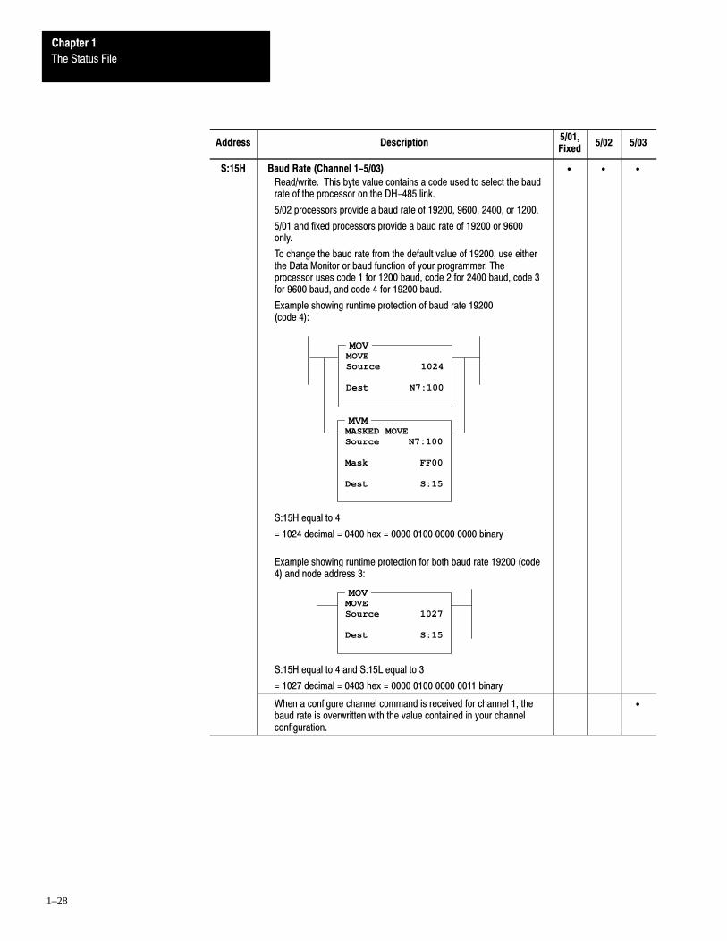
Chapter 1
The Status File
1–28
Address Description5/01,Fixed
5/02 5/03
S:15H Baud Rate (Channel 1-5/03)
Read/write. This byte value contains a code used to select the baudrate of the processor on the DH-485 link.
5/02 processors provide a baud rate of 19200, 9600, 2400, or 1200.
5/01 and fixed processors provide a baud rate of 19200 or 9600only.
To change the baud rate from the default value of 19200, use eitherthe Data Monitor or baud function of your programmer. Theprocessor uses code 1 for 1200 baud, code 2 for 2400 baud, code 3for 9600 baud, and code 4 for 19200 baud.
Example showing runtime protection of baud rate 19200(code 4):
S:15H equal to 4 and S:15L equal to 3
= 1027 decimal = 0403 hex = 0000 0100 0000 0011 binary
S:15H equal to 4
= 1024 decimal = 0400 hex = 0000 0100 0000 0000 binary
Example showing runtime protection for both baud rate 19200 (code4) and node address 3:
MOVMOVESource 1027
Dest S:15
MVMMASKED MOVESource N7:100
Mask FF00
Dest S:15
MOVMOVESource 1024
Dest N7:100
• • •
When a configure channel command is received for channel 1, thebaud rate is overwritten with the value contained in your channelconfiguration.
•

Chapter 1
The Status File
1–29
Address Description5/01,Fixed
5/02 5/03
S:16 and S:17
Test Single Step - Start Step On - Rung/File
Read only. These registers indicate the executable rung (word S:16)and file (word S:17) number that the processor will execute next whenoperating in the Test Single Step mode. To enable this feature, youmust select the Test Single Step option at the time you save yourprogram.
These values are updated upon completion of every rung. Refer toWord S:2/4 for more information. Your programming deviceinterrogates this value when providing �start step on file x, rung y"status line information. There is no known use for this feature whenaddressed by your ladder program.
The Test Single Step mode is discussed in chapter 17 in theAdvanced Programming Software User Manual, Catalog Number1747-NM002.
• •
This feature is built into the 5/03 processor. Selection is not required. •S:18 and S:19
Test Single Step - Breakpoint - Rung/File
Read only. These registers indicate the executable rung (word S:18)and file (word S:19) number that the processor should stop in front ofwhen executing in the Test Single Step mode. To enable this feature,you must select the Test Single Step option at the time you save yourprogram.
If both the rung and file number are 0, the processor will step to thenext rung only; otherwise the processor will continue until it finds arung/file equaling the S:18/S:19 value.
The processor stops, then clears S:18 and S:19 when it finds amatch, while remaining in the Test Single Step mode. The processorwill operate indefinitely if it cannot find the end rung/file that you haveentered. It operates until it finds a match, receives a mode change, orpowers down. See S:2/4.
Your programming device interrogates this value when providing �endstep before file x, rung y" status line information. Your programmingdevice also writes this value when prompting you for �set end rung."There is no known use for this feature when addressed by yourladder program.
The Test Single Step mode is discussed in chapter 17 in theAdvanced Programming Software User Manual, Catalog Number1747-NM002.
• •
This feature is built into the 5/03 processor. Selection is not required. •

Chapter 1
The Status File
1–30
Address Description5/01,Fixed
5/02 5/03
S:20 and S:21
Test - Fault/Powerdown - Rung/File
Read/write. These registers indicate the executable rung (word S:20)and file (word S:21) number that the processor last executed before amajor error or powerdown occurred. To enable this feature, you mustselect the Test Single Step option at the time you save your program.You can use these registers to pinpoint the execution point of theprocessor at the last powerdown or fault routine entry. This function isalso active in the REM Run mode. See S:2/4.
Application example: Suppose your program contains several TONinstructions. TON T4:6 in file 2, rung 25 occasionally obtains anegative preset. Recovery from the negative preset fault is possibleby placing the preset at 100 and resetting the timer.
Place the following rung in your fault routine to accomplish this. BitB3/0 is latched as evidence that an application recovery has beeninitiated.
• •
This feature is built into the 5/03 processor. Selection is not required. •
MOVMOVESource 100
Dest T4:6.PRE
EQUEQUALSource A S:6
Source B 52
(RET)
(RES)T4:6
(L)B3
0
(U)S:1
13
File NumberThe value 52 equals 0034 Hex.This is the error code for anegative timer preset.
EQUEQUALSource A S:20
Source B 25
EQUEQUALSource A S:21
Source B 2
Rung Number

Chapter 1
The Status File
1–31
Address Description5/01,Fixed
5/02 5/03
S:22 Maximum Observed Scan Time
Read/write. This word indicates the maximum observed intervalbetween consecutive scans.
Consecutive scans are defined as intervals between file 2/rung 0 andthe END, TND, or the REF instruction. This value indicates, in 10 msincrements, the time elapsed in the longest program cycle of theprocessor. The processor compares each last scan value to the valuecontained in S:22. If the processor determines that the last scan valueis larger than the value stored at S:22, the last scan value is written toS:22.
Resolution of the maximum observed scan time value is +0 to −10 ms. For example, the value 9 indicates that 80-90 ms wasobserved as the longest program cycle.
Interrogate this value using the Data Monitor function if you need todetermine or verify the longest scan time of your program.
Important: The I/O scan, processor overhead, and communicationservicing is not included in this measurement.
• •
The Scan Time Selection Bit (S:33/13) determines the timebase usedfor average and maximum Scan Times. When clear, operation is asdescribed above. When set, the timebase is expressed in 1 msincrements (instead of 10 ms increments). When S:33/13 is set,resolution of the maximum observed scan time value is +0 to −1 ms.For example, the value 9 indicates that 8 to 9 ms was observed asthe largest program cycle.
•
S:23 Average Scan Time
Read/write. This word indicates a weighted running average time.The value indicates, in 10 ms increments, the time elapsed in theaverage program cycle of the processor. For every Scan t:
Avg = (Avg * 7) + Scan t 8
Resolution of the average scan time value is +0 to −10 ms. Forexample, the value 2 indicates that 10 to 20 ms was calculated as theaverage program cycle.
Important: The I/O scan, processor overhead, and communicationservicing is not included in this measurement.
• •
The Scan Time Selection bit S:33/13 determines the timebase usedfor average Scan time. When clear, operation is as described above.When set, the timebase is expressed in 1 ms increments (instead of10 ms increments). When S:33/13 is set, resolution of the averagescan time value is +0 to -1 ms. For example: The value 2 indicatesthat 1 to 2 ms was calculated as the average program cycle.
•
S:24 Index Register
Read/write. This word indicates the element offset used in indexedaddressing. Refer to chapter 5 in the Advanced ProgrammingSoftware User Manual, Catalog Number 1747-NM002.
When an STI, I/O Slot, or Fault Routine interrupts normal execution ofyour program, the original value of this register is restored whenexecution resumes.
• •
When a DII interrupts normal execution of your program, the originalvalue of this register is restored when execution resumes.
•

Chapter 1
The Status File
1–32
Address Description5/01,Fixed
5/02 5/03
S:25andS:26
I/O Interrupt Pending
Read only. These two words are bit�mapped to the 30 I/O slots. BitsS:25/1 through S:26/14 refer to slots 1-30. Bits S:25/0 and S:26/15are reserved.
The pending bit associated with an interrupting slot is set when thecorresponding I/O Slot Interrupt Enable bit is clear at the time of aninterrupt request. It is cleared when the corresponding I/O EventInterrupt Enable bit is set, or when an associated RPI instruction isexecuted.
The pending bit for an executing I/O interrupt subroutine remainsclear when the ISR is interrupted by an STI or fault routine. Likewise,the pending bit remains clear if interrupt service is requested at thetime that a higher or equal priority interrupt is executing (fault routine,STI, or other ISR).
I/O interrupts are discussed in chapter 19 of this manual.
• •
The pending bit associated with an interrupting slot is set when thecorresponding I/O Slot Interrupt Enable bit is clear at the time of aninterrupt request. It is cleared when the corresponding I/O EventInterrupt Enable bit is set, or when an associated RPI instruction isexecuted. The pending bit will always be set when interrupt service isrequested and the processor is executing an interrupt of equal orhigher priority. Interrupt priority will not effect the setting of these bits.
For example, while executing an STI subroutine, slot 6 requests anI/O Event Interrupt. The STI will execute to completion; however, slot6 pending bit (S:25/6) will become set within execution of the STI.Examine the state of these bits within your interrupt subroutines ifyour application requires this information.
•
S:27andS:28
I/O Interrupt Enabled
Read/write. These two words are bit�mapped to the 30 I/O slots. BitsS:27/1 through S:28/14 refer to slots 1-30. Bits S:27/0 and S:28/15are reserved.
The default value of each bit is 1 (set). The enable bit associated withan interrupting slot must be set when the interrupt occurs to allow thecorresponding ISR to execute. Otherwise, the ISR will not executeand the associated I/O slot interrupt pending bit will become set.
Changes made to these bits using the Data Monitor function or ladderinstructions other than IID or IIE take affect at the next end of scan.
I/O interrupts are discussed in chapter 19 of this manual.
• •
These bits may be set/reset by the user program, comms., or with theIIE or IID instruction. Changes made to these bits using aprogramming terminal's Data Monitor function or any ladderinstruction take affect immediately.
•
S:29 User Fault Routine File Number
Read/write. You enter a program file number (3-255) to be used in allrecoverable and non�recoverable major errors. Program the ladderlogic of your fault routine in the file you have specified. Write a 0 valueto disable the fault routine.
To provide protection from inadvertent Data Monitor alteration of yourselection, program an unconditional MOV instruction containing theprogram file number of your fault routine to S:29, or program a CLRinstruction at S:29 to prevent fault routine operation.
The fault routine is discussed in chapter 16 of this manual.
• •

Chapter 1
The Status File
1–33
Address Description5/01,Fixed
5/02 5/03
S:30 Selectable Timed Interrupt - Setpoint
Read/Write. You enter the timebase, in tens of milliseconds, to beused in the selectable timed interrupt. Your STI routine executes perthe value you enter. Write a zero value to disable the STI.
To provide protection from inadvertent Data Monitor alteration of yourselection, program an unconditional MOV instruction containing thesetpoint value of your STI to S:30, or program a CLR instruction atS:30 to prevent STI operation.
If the STI is initiated while in the REM Run mode by loading the statusregisters, the interrupt starts timing from the end of the program scanin which the status registers were loaded.
Selectable timed interrupts are discussed in chapter 18 of thismanual.
• •
The STI Setpoint timebase can be either 10 ms or 1 ms depending onthe value of the STI Setpoint Selection bit S:2/10. When clear,operation is as described above. When set, the timebase isexpressed in 1 ms increments. The STE and STD disables the STIinstruction.
•
S:31 Selectable Timed Interrupt - File Number
Read/write. You enter a program file number (3-255) to be used asthe selectable timed interrupt subroutine. Write a 0 value to disablethe STI.
To provide protection from inadvertent Data Monitor alteration of yourselection, program an unconditional MOV instruction containing thefile number value of your STI to S:31, or program a CLR instruction atS:31 to prevent STI operation.
Selectable timed interrupts are discussed in chapter 18 of thismanual.
• •
S:32 I/O Interrupt Executing
Read only. This word indicates the slot number of the specialty I/Omodule that generated the currently executing ISR. This value iscleared upon completion of the ISR, REM Run mode entry, or uponpower up.
You can interrogate this word inside of your STI subroutine or faultroutine if you wish to know if these higher priority interrupts haveinterrupted an executing ISR. You may also use this value to discerninterrupt slot identity when multiplexing two or more specialty I/Omodule interrupts to the same ISR.
I/O interrupts are discussed in chapter 19 of this manual.
• •
You can integrate this word inside your DII subroutine if you wish toknow if these higher priority interrupts have interrupted an executingISR. You may also use this value to discern interrupt slot identitywhen multiplexing two or more specialty I/O module interrupts to thesame ISR.
•
S:33/0 Incoming Command Pending (Channel 0)
Read only. This bit becomes set when the processor determines thatanother node on the channel 0 network has requested information orsupplied a command to it. This bit can be set at any time. This bit iscleared when the processor services the request (or command).
Use this bit as a condition of an SVC instruction to enhance thecommunication capability of your processor.
•

Chapter 1
The Status File
1–34
Address Description5/01,Fixed
5/02 5/03
S:33/1 Message Reply Pending (Channel 0)
Read only. This bit becomes set when another node on the channel0 network has supplied the information that you requested in theMSG instruction of your processor. This bit is cleared when theprocessor stores the information and updates your MSG instruction.
Use this bit as a condition of an SVC instruction to enhance thecommunication capability of your processor.
•
S:33/2 Outgoing Message Command Pending (Channel 0)
Read only. This bit is set when one or more channel 0 messages inyour program are enabled and waiting, but no message is beingtransmitted at the time. As soon as transmission of a messagebegins, the bit is cleared. After transmission, the bit is set again ifthere are further messages waiting, or it remains cleared if there areno further messages waiting.
•
S:33/3 Selection Status (Channel 0)
Read only. When set, this bit indicates that the channel 0communication port is in the User mode (ASCII mode). When clear,this bit indicates that channel 0 is in the System mode (DF1 mode).Use your programming devices channel configuration utility to changethis selection.
•
S:33/4 Communications Active (Channel 0)
Read only. This bit is set by the processor when at least one othernode is active on channel 0. Otherwise the bit remains cleared.
•
S:33/5 Communications Servicing Selection (Channel 0)
Read/write. When set, only one channel 0 communication request/command will be serviced per END, TND, REF, or SVC instruction.When clear, all serviceable incoming or outgoing communicationrequests/commands will be serviced per END, TND, REF, or SVCinstruction.
One communication request/command consists of either a channel 0Incoming Command, channel 0 Message Reply, or channel 0Outgoing Message Command. Refer to Words S:33/0, S:33/1, S:33/2,and S:33/6 for more information.
Note: When clear, your communication throughput will increase.Your scan time will also increase if several communicationcommands/requests are received in the same scan.
To program this feature, use the Data Monitor function to set andclear this bit. To provide protection from inadvertent data monitoralteration of your selection, program an unconditional OTL instructionat address S:33/5 to ensure one request/command operation, or anunconditional OTU instruction at address S:33/5 to ensure multiplerequest/command operation. Alternately, your program may changethe state of this bit using ladder logic if your application requiresdynamic selection of this function.
•
S:33/6 Message Servicing Selection (Channel 0)
Read/write. This bit is only valid when the channel 0 CommsServicing Selection (S:33/5) is clear (which selects service allcommands). When S:33/6 is set and S:33/5 is clear, all outgoingchannel 0 MSG instructions will be serviced per END, TND, SVC, orREF instruction. Otherwise, only one outgoing channel 0 MSGcommand or reply will be serviced per END, TND, SVC, or REFinstruction.
•
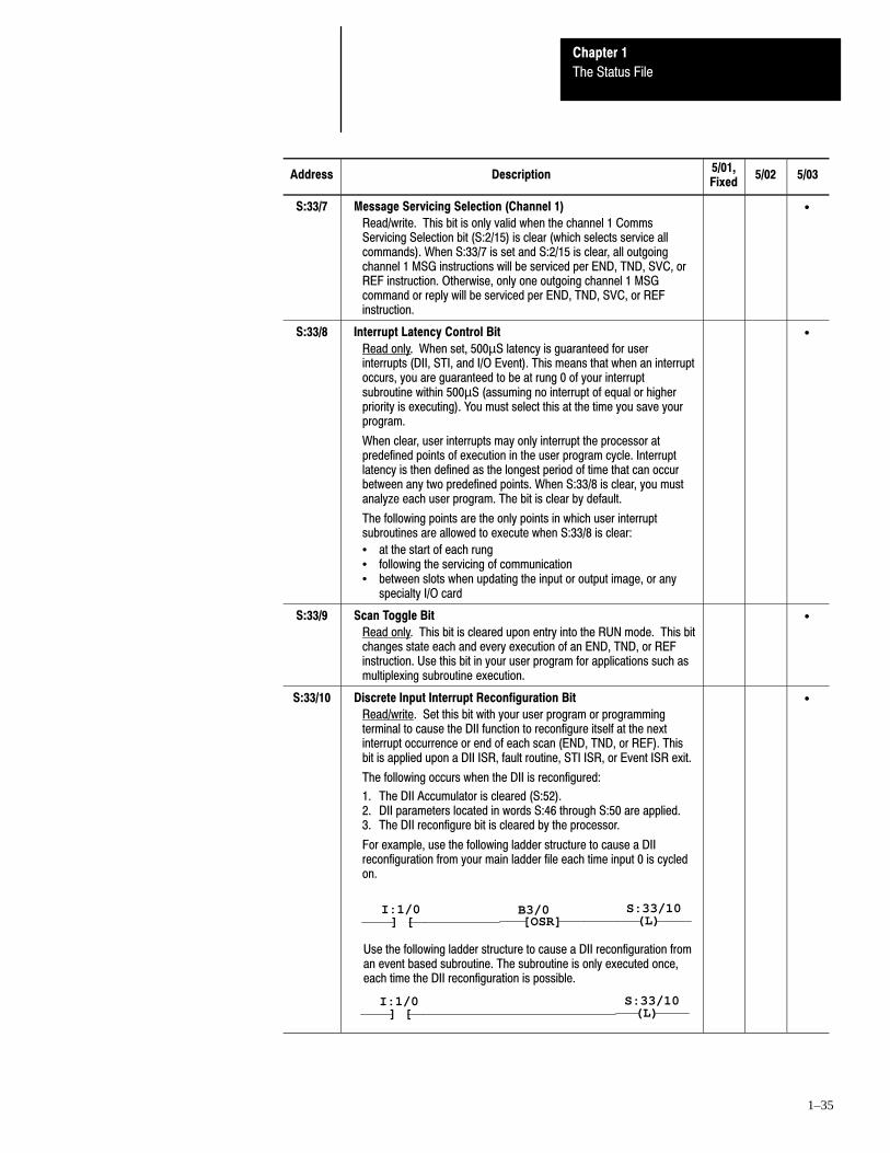
Chapter 1
The Status File
1–35
Address Description5/01,Fixed
5/02 5/03
S:33/7 Message Servicing Selection (Channel 1)
Read/write. This bit is only valid when the channel 1 CommsServicing Selection bit (S:2/15) is clear (which selects service allcommands). When S:33/7 is set and S:2/15 is clear, all outgoingchannel 1 MSG instructions will be serviced per END, TND, SVC, orREF instruction. Otherwise, only one outgoing channel 1 MSGcommand or reply will be serviced per END, TND, SVC, or REFinstruction.
•
S:33/8 Interrupt Latency Control Bit
Read only. When set, 500µS latency is guaranteed for userinterrupts (DII, STI, and I/O Event). This means that when an interruptoccurs, you are guaranteed to be at rung 0 of your interruptsubroutine within 500µS (assuming no interrupt of equal or higherpriority is executing). You must select this at the time you save yourprogram.
When clear, user interrupts may only interrupt the processor atpredefined points of execution in the user program cycle. Interruptlatency is then defined as the longest period of time that can occurbetween any two predefined points. When S:33/8 is clear, you mustanalyze each user program. The bit is clear by default.
The following points are the only points in which user interruptsubroutines are allowed to execute when S:33/8 is clear:
• at the start of each rung• following the servicing of communication• between slots when updating the input or output image, or any
specialty I/O card
•
S:33/9 Scan Toggle Bit
Read only. This bit is cleared upon entry into the RUN mode. This bitchanges state each and every execution of an END, TND, or REFinstruction. Use this bit in your user program for applications such asmultiplexing subroutine execution.
•
S:33/10 Discrete Input Interrupt Reconfiguration Bit
Read/write. Set this bit with your user program or programmingterminal to cause the DII function to reconfigure itself at the nextinterrupt occurrence or end of each scan (END, TND, or REF). Thisbit is applied upon a DII ISR, fault routine, STI ISR, or Event ISR exit.
The following occurs when the DII is reconfigured:
1. The DII Accumulator is cleared (S:52).2. DII parameters located in words S:46 through S:50 are applied.3. The DII reconfigure bit is cleared by the processor.
For example, use the following ladder structure to cause a DIIreconfiguration from your main ladder file each time input 0 is cycledon.
[OSR]B3/0
] [I:1/0
(L)S:33/10
Use the following ladder structure to cause a DII reconfiguration froman event based subroutine. The subroutine is only executed once,each time the DII reconfiguration is possible.
] [I:1/0
(L)S:33/10
•

Chapter 1
The Status File
1–36
Address Description5/01,Fixed
5/02 5/03
S:33/11and
S:33/12
Online Edit Status
Read only. These two bits represent the four possible Online Editstates:
Bit 12 Bit 11 Online Edit Status0 0 No online edits exist0 1 Online edits are disabled1 0 Reserved1 1 Testing online edits
Examine the state of these bits with your user program to count thenumber of online edit sessions, flag an alarm, or place yourapplication in a special state designed for online edit sessions.
•
S:33/13 Scan Time Timebase Selection
Read/write. This bit determines the timebase used to average theScan time (S:23) and the maximum Scan Time (S:22). When clear,the value contained in the average and maximum scan timesrepresent the number of 10 ms increments that have occurred. Whenset, the value contained in the average and maximum scan timesrepresent the number of 1 ms increments that have occurred. Thisvalue is clear by default (10 ms timebase).
•
S:33/14 DTR Control Bit (Channel 0)
Read/write. This bit is used to enable DTR dialing. When clear, thechannel 0 DTR signal (pin 4) is directly controlled by the standardcommunication driver. When set, you can perform DTR dialing bywriting to S:33/15, DTR Force Bit.
Bit S:33/14 is examined and applied at each end of scan (END, TND,or REF). When in Program, Suspend, or Fault mode, DTR is enabledand remains enabled until an auto-disconnect sequence is detectedby the communication driver.
An auto-disconnect occurs if the communication driver detects thatchannel 0 CD signal (pin 1) has been absent for more than 10seconds or if the channel 0 DSR signal (pin 6) has been disabled.Refer to S:5/14 Channel 0 Modem Lost bit for more information.During an auto-disconnect, the standard communication driver keepsthe DTR disabled until either the channel 0 DSR signal is enabled, or5 seconds elapse.
Important: When channel 0 is configured for DH485, S:33/14 mustbe clear for proper operation.
•
S:33/15 DTR Force Bit (Channel 0)
Read/write. This bit is used to force the DTR pin high or low. WhenS:33/14 is set, the channel 0 DTR signal (pin 4) is applied at eachend of scan (END, TND, or REF) using the state of S:33/15. WhenS:33/14 is clear, this bit has no effect on DTR.
When S:33/15 is set, DTR is forced high. When clear (default,) DTR isforced low. When in the REM Test or REM Run mode, this bit is onlyapplied at end of scan (END, TND, or REF). When in Program,Suspend, or Fault mode (or on power up), DTR is set unless thecommunication driver is performing an auto-disconnect.
•
S:34 Reserved •

Chapter 1
The Status File
1–37
Address Description5/01,Fixed
5/02 5/03
S:35 Last 1 ms Scan Time
Read only. The value of this word tells you how much time elapses ina program cycle. A program cycle includes the ladder program,housekeeping, I/O scan, and servicing of the communication port.This word value is only updated by the processor once each scan,immediately preceding the execution of rung 0, file 2 (or upon returnof a REF instruction).
•
S:36/0 toS:36/7
Reserved
Read/write.•
S:36/8 DII Lost
Read/write. This bit is set anytime a DII interrupt occurs while the DIIPending bit (S:2/11) is also set. When set, you are notified that a DIIinterrupt has been lost. For example, the interrupt is lost because aprevious interrupt was already pending and waiting execution.Examine this bit in your user program and take appropriate action ifyour application cannot tolerate this condition. Then clear this bit withyour user program to prepare for the next possible occurrence of thiserror.
•
S:36/9 STI Lost
Read/write. This bit is set anytime an STI interrupt occurs while theSTI Pending bit (S:2/0) is also set. When set, you are notified that aSTI interrupt has been lost. For example, the interrupt is lost becausea previous interrupt was already pending and waiting execution.Examine this bit in your user program and take appropriate action ifyour application cannot tolerate this condition. Then clear this bit withyour user program to prepare for the next possible occurrence of thiserror.
•
S:36/10 Memory Module Data File Overwrite Protection
Read/write. Use this bit to determine the validity of retentive datafollowing a memory module transfer. This bit is always set when amemory module to processor transfer occurs with Data File OverwriteProtection selected and protected files are overwritten. Protected filesare overwritten anytime a memory module program does not matchthe processor program at the time of the transfer. This bit is notcleared by the processor.
•
S:36/11to
S:36/15
Reserved for additional minor errors. •
S:37 Clock/Calendar Year
Read/write. This value contains the year value of the clock/calendar.Valid range is 0-65535. To disable the clock/calendar, write zeros toall clock/calendar words (S:37 to S:42).
•
S:38 Clock/Calendar Month
Read/write. This value contains the month value of the clock/calendar. Valid range is 1-12. To disable the clock/calendar, writezeros to all clock or calendar words (S:37 to S:41). January equalsthe value of 1.
•
S:39 Clock/Calendar Day
Read/write. This value contains the day value of the clock/calendar.Valid range is 1-31. To disable the clock/calendar, write zeros to allclock or calendar words (S:37 to S:41). The first day of the monthequals the value of 1.
•
Chapter 1
The Status File
1–38
Address Description5/01,Fixed
5/02 5/03
S:40 Clock/Calendar Hours
Read/write. This value contains the hour value of the clock/calendar.Valid range is 0-23. To disable the clock/calendar, write zeros to allclock or calendar words (S:37 to S:41). 0000 hundred hours equalsthe value of 0.
•
S:41 Clock/Calendar Minutes
Read/write. This value contains the minute value of theclock/calendar. Valid range is 0-59. To disable the clock/calendar,write zeros to all clock or calendar words (S:37 to S:41).
•
S:42 Clock/Calendar Seconds
Read/write. This value contains the seconds value of theclock/calendar. Valid range is 0-59. To disable the clock/calendar,write zeros to all clock or calendar words (S:37 to S:41).
•
S:43 toS:45
Reserved •
S:46 Discrete Input Interrupt - File Number
Read/write. You enter a program file number (3-255) to be used asthe discrete input interrupt subroutine. Write a 0 value to disable thefunction. This bit is applied upon detection of a DII Reconfigure bit,each DII ISR exit, and each end of scan (END, TND, or REF).
To provide protection from inadvertent data monitor alteration of yourselection, program an unconditional MOV instruction containing thefile number value of your DII to S:46 or program a CLR instruction atS:46 to prevent DII operation.
•
S:47 Discrete Input Interrupt - Slot Number
Read/write. You enter the slot number (1-30) that contains theDiscrete I/O module to be used as the discrete input interrupt slot.The processor will fault if the slot is empty or contains a non-discreteI/O module. For example, an analog module causes a processor faultto occur. This bit is applied upon detection of the DII Reconfigure bit.
This value is only applied upon execution of the DII reconfigurationfunction (setting bit S:33/10 or upon REM Run mode entry with theDII Enable bit S:2/12 set).
To provide protection from inadvertent data monitor alteration of yourselection, program an unconditional MOV instruction containing theslot number value of your DII to S:47.
•
S:48 Discrete Input Interrupt - Bit Mask
Read/write. You enter a bit mapped value that corresponds to the bitsthat you wish to monitor on the discrete I/O module. Only bits 0 to 7are used in the DII function. Setting a bit indicates that you wish toinclude the bit in the comparison of the discrete I/O module's bittransition to the DII Compare Value (S:49). Clearing a bit indicatesthat the transition state of that particular bit is a �don't care" bit. Thisbit is applied upon detection of a DII Reconfigure bit, each DII ISRexit, and at each end of scan (END, TND, or REF).
To provide protection from inadvertent data monitor alteration of yourselection, program an unconditional MOV instruction containing thebit mask value of your DII to S:48.
•
Chapter 1
The Status File
1–39
Address Description5/01,Fixed
5/02 5/03
S:49 Discrete Input Interrupt - Compare Value
Read/write. You enter a bit mapped value that corresponds to the bittransitions that must occur in the discrete I/O card for a count orinterrupt to occur. Only bits 0 to 7 are used in the DII function. Settinga bit indicates that the bit must transition from a 0 to a 1 to satisfy thecompare condition for that bit. Clearing a bit indicates that the bitmust transition from a 1 to a 0 in order to satisfy the comparecondition for that bit. An interrupt or count will be generated upon thelast bit transition of the compare value. This bit is applied upondetection of a DII Reconfigure bit, each DII ISR exit, and each end ofscan (END, TND, or REF).
To provide protection from inadvertent data monitor alteration of yourselection, program an unconditional MOV instruction containing thebit mask value of your DII to S:49.
•
S:50 Discrete Input Interrupt - Preset
Read/write. When this value is equal to 0 or 1, an interrupt isgenerated each time the bit transitions specific words in S:48 andS:49. When this value is between 2-32767, a count occurs each timethe bit transition comparison cycle is satisfied. An interrupt isgenerated when the preset value reaches 1. This bit is applied upondetection of a DII Reconfigure bit, each DII ISR exit, and at each endof scan (END, TND, or REF).
To provide protection from inadvertent data monitor alteration of yourselection, program an unconditional MOV instruction containing thepreset value of your DII to S:50.
•
S:51 Discrete Input Interrupt - Return Mask
Read only. The return mask is updated immediately preceding entryinto the DII subroutine. This value contains the bit map of the bittransitions that caused the interrupt. The bit is set if it was included inthe list of bit transitions that caused the interrupt, (specified totransition in the S:48 and S:49 comparisons). The bit is cleared if itwas masked. This value is cleared by the processor upon exit of theDII subroutine.
Use this value to validate the interrupt transitions. Or whendynamically reconfiguring (sequencing) the DII, you can use thisvalue inside your DII's subroutine to help determine or validate itsposition in the sequence.
•
S:52 Discrete Input Interrupt - Accumulator
Read only. The DII accumulator contains the number of down counttransitions that have occurred (see S:50.) When a down count occurs,and the accumulator is greater than or equal to the down count value,a DII interrupt is generated.
•
S:53 andS:54
Reserved •
S:55 Last Discrete Input Interrupt Scan Time
Read/write. This value indicates, in 1 ms increments, the amount oftime elapsed by the most recent DII subroutine. The resolution of thisvalue is +0 to −1 ms.
•

Chapter 1
The Status File
1–40
Address Description5/01,Fixed
5/02 5/03
S:56 Maximum Observed Discrete Input Scan Time
Read/write. This value indicates, in 1 ms increments, the maximumamount of time elapsed by any single DII subroutine execution. Theprocessor compares each last DII scan value (S:55) to the maximumDII scan value contained in S:56. If the processor determines that thelast DII scan value is larger than the value stored at S:56, the lastscan value (S:55) is written to S:56, thus becoming the new maximumDII scan time. The resolution of this value is +0 to −1 ms.
Interrogate this value using a programming device Data Monitorfunction if you need to determine or verify the longest scan time ofyour program.
•
S:57 Operating System Catalog Number
Read only. Indicates the operating system catalog number. Forexample, the value of 300 indicates operating system -OS300, thevalue of 301 indicates -OS301.
•
S:58 Operating System Series
Read only. Indicates the operating system series. For example, thevalue of 0 indicates series A and the value of 1 indicates series B.
•
S:59 Operating System FRN
Read only. Indicates the operating system firmware release number.For example, the value of 1 indicates FRN1 and the value of 2indicates FRN2.
•
S:60 Processor Catalog Number
Read only. Indicates the catalog number of the processor. Forexample, the value of 532 indicates -L532 and the value of 534indicates -L534.
•
S:61 Processor Series
Read only. Indicates the processor series. For example, the value of0 indicates series A and the value of 1 indicates series B.
•
S:62 Processor Revision
Read only. Indicates the processor revision. For example, the valueof 1 indicates REV1 and the value of 2 indicates REV2.
•
S:63 User Program Type
Read only. Indicates the programming device that created the userprogram. For example, at initial release the value of 1 indicates APS4.xx.
•
S:64 User Program Functionality Index
Read only. Indicates the level of functionality contained in a givenprogram type. For example, at initial release the value of 5 indicatesAPS 4.xx.
•
S:65 User RAM Size
Read only. Indicates the size of NVRAM in 16 bit K words. Forexample the value of 64 equals 64K words of NVRAM.
•
S:66 Flash EEPROM Size
Read only. Indicates the size of operating system memory in 16 bit Kwords. For example the value of 128 equals 128K words of memory.
•
S:67 toS:83
Channel 0 Active Nodes
Read only. •

Chapter 1
The Status File
1–41
The two status file displays apply to the 5/02 and 5/03 processors; however,only the first display applies to the 5/01 and fixed processors. The 5/03processor has two additional displays, which are shown on the followingpage.
The displays are accessible offline and online under the Data Monitor orGeneral Utility function. Move between displays by pressing the [ Pg Dn ]or [ Pg Up ] keys of the terminal.
ARITHMETIC FLAGS S:0 Z:0 V:0 C:0
PROCESSOR STATUS 00000000 00000000 SUSPEND CODE 0PROCESSOR STATUS 00000000 00000001 SUSPEND FILE 0PROCESSOR STATUS 00000000 00000000 WATCHDOG [x10 ms] 10MINOR FAULT 00000000 00000000 LAST SCAN [x10 ms] 0FAULT CODE 0000 FREE RUNNING CLOCK 00000000 00000000FAULT DESCRIPTION:
MATH REGISTER 0000 0000
ACTIVE NODE LIST (CHANNEL 1) I/O SLOT ENABLES0 10 20 30 0 10 20 3011000000 00000000 00000000 00000000 11111111 11111111 11111111 11111111
PROCESSOR BAUD RATE (CHANNEL 1) 19200 PROCESSOR ADDRESS (CHANNEL 1) 1
Press function key or enter value, press Alt–H for help.S:0/0 = offline no forces formatted decimal addr File 09TEST
Message:Prompt:Data/Cmd Entry:Status:
Main Functions:
F7F5
NEXTFILE
SPECIFYADDRESS
F9 F10F8
CLR MINFAULT
CLR MAJFAULT
PREVFILE
Display Area:
F1
PAGEUP
F2
PAGEDOWN
LAST SCAN (x01 ms) 0 I/O SLOT INTERRUPT ENABLESLAST SCAN [x10 ms]: 0 0 10 20 301 ms TIMEBASE (SCAN Times) 0 00000000 00000000 00000000 00000000AVERAGE SCAN [x10 ms]: 0 MAXIMUM SCAN [x10 ms]: 1
I/O SLOT INTERRUPT PENDINGINDEX REGISTER VALUE: 4 0 10 20 30INDEX ACROSS FILES: NO 00000000 00000000 00000000 00000000 FAULT ROUTINE SUBROUTINE FILE: 0 I/O INTERRUPT FILE EXEC: 0
SELECTABLE TIMED INTERRUPT SINGLE STEP TEST FILE RUNG SUBROUTINE FILE: 0 START STEP ON: 2 3 SETPOINT [x10 ms]: 0 END STEP BEFORE: 0 0 ENABLED: 1 FAULT/POWER DOWN: 2 3 EXECUTING: 0 COMPILED FOR SINGLE STEP: YES PENDING: 0 1 ms TIMEBASE 0
Display Area:
F7F5 F8
NEXTFILE
SPECIFYADDRESS
Press function key or enter value, press Alt–H for help.S:28/15 = offline no forces formatted decimal addr File 09TEST
Message:Prompt:Data/Cmd Entry:Status:
Main Functions:PREVFILE
F1 F2
PAGEUP
PAGEDOWN
Status File Display
Chapter 1
The Status File
1–42
Additional 5/03 Status File Displays
EXT PROCESSOR STATUS 0000000 00000000 REAL TIME CLOCK DATE: 10–18–1992EXT MINOR FAULT 0000000 00000000 TIME: 2:15.34
DISCRETE INPUT INTERRUPT SUBROUTINE FILE: 3 MASK: 00000001 INPUT SLOT: 1 COMPARE VALUE: 00000001 ENABLED 1 PRESET: 1 EXECUTING: 0 RETURN MASK: 00000000 PENDING: 0 ACCUMULATOR: 0 OVERFLOW: 0 LAST SCAN [ms]: 0
MAX. SCAN [ms]: 0
PROCESSOR OPERATING SYSTEM USER PROGRAM CATALOG #: 0 CATALOG #: 0 FUNCTIONAL TYPE: 0 SERIES: 0 SERIES: 0 FUNCTIONAL INDEX: 0 REVISION: 0 F.R.N.: 0 USER RAM SIZE: 0 FLASH EEPROM SIZE: 0
Display Area:
Press function key or enter value, press Alt–H for help.S:0/0 = offline no forces formatted decimal addr File 09TEST
Message:Prompt:Data/Cmd Entry:Status:
Main Functions:
F7F5 F8
NEXTFILE
SPECIFYADDRESS
PREVFILE
F1 F2
PAGEUP
PAGEDOWN
0–31 00000000 00000000 00000000 00000000 32–63 00000000 00000000 00000000 00000000 64–95 00000000 00000000 00000000 00000000 96–127 00000000 00000000 00000000 00000000128–159 00000000 00000000 00000000 00000000160–191 00000000 00000000 00000000 O0000000192–223 00000000 00000000 00000000 00000000224–255 00000000 00000000 00000000 00000000
Display Area:
0 10 20 30
Press function key or enter value, press Alt–H for help.S:0/0 = offline no forces formatted decimal addr File 09TEST
Message:Prompt:Data/Cmd Entry:Status:
Main Functions:
CHANNEL 0 ACTIVE NODE TABLE
F7F5 F8
NEXTFILE
SPECIFYADDRESS
PREVFILE
F1 F2
PAGEUP
PAGEDOWN

A–B 2Chapter
2–1
Instruction Set Overview
This chapter takes a brief look at the instruction set, listing the name,mnemonic, and function of each instruction. Instructions that are specific toa certain processor are also indicated.
Important: To avoid misapplication, do not apply any of the instructionsuntil you have read the detailed descriptions in chapters 3through 14.
An instruction locator is provided on page 2–9. This is a list of theinstruction mnemonics, in alphabetical order, with page references.
The instruction set is divided into the classifications named in chapters 3through 14. A brief description of the individual instructions in eachclassification follows.
Bit Instructions - Chapter 3
Instruction Mnemonicand Name
5/01,Fixed
5/02 5/03Function -
Conditional InstructionsInput or Output
XIC Examine if Closed • • • Conditional instruction. True when bit is on (1).
XIO Examine if Open • • • Conditional instruction. True when bit is off (0).
OSR One Shot Rising • • • Conditional instruction. Makes rung true for one scanupon each false�to�true transition of conditionspreceding it in the rung.
OTE Output Energize • • • Output instruction. True (1) when conditionspreceding it are true. False when conditionspreceding it go false.
OTL Output Latch • • • Output instruction. Addressed bit goes true (1) whenconditions preceding the OTL instruction are true.When conditions go false, OTL remains true until therung containing an OTU instruction with the sameaddress goes true.
OTU Output Unlatch • • • Output instruction. Addressed bit goes false (0)when conditions preceding the OTU instruction aretrue. Remains false until the rung containing an OTLinstruction with the same address goes true.
Instruction Classifications

Chapter 2
Instruction Set Overview
2–2
Timer and Counter Instructions - Chapter 4
Instruction Mnemonic
and Name
5/01,Fixed
5/02 5/03Function -
Output Instructions
TON Timer On�Delay • • • Counts time intervals when conditions preceding it inthe rung are true. Produces an output whenaccumulated value (count) reaches the preset value.
TOF Timer Off�Delay • • • Counts time intervals when conditions preceding it inthe rung are false. Produces an output whenaccumulated value (count) reaches the preset value.
RTO Retentive Timer • • • This is an On�Delay timer that retains its accumulatedvalue when:- rung conditions go false.- the mode changes to program from run or test.- the processor loses power.- a fault occurs.
CTU Count Up • • • Counts up for each false�true transition of conditionspreceding it in the rung. Produces an output whenaccumulated value (count) reaches the preset value.
CTD Count Down • • • Counts down for each false�true transition ofconditions preceding it in the rung. Produces anoutput when accumulated value (count) reaches thepreset value.
HSC High-Speed Counter • • • Applies to 24 VDC fixed I/O controllers only. Countshigh-speed pulses from a high-speed input.Maximum pulse rate of 8kHz.
RES Reset • • • Used with timers and counters. When conditionspreceding it in the rung are true, the RES instructionresets the accumulated value and control bits of thetimer or counter.

Chapter 2
Instruction Set Overview
2–3
Communication Instructions - Chapter 5
Instruction Mnemonic
and Name
5/01,
Fixed5/02 5/03
Function -
Output Instructions
MSG Message Read/Write • • This instruction transfers data from one node toanother on the communication network. When theinstruction is enabled, message transfer is pending.Actual data transfer takes place at the end of thescan.
SVC Service
Communications
• • When conditions preceding it in the rung are true, theSVC instruction interrupts the program scan toexecute the service communication portion of theoperating cycle.
I/O and Interrupt Instructions - Chapter 6
Instruction Mnemonic
and Name
5/01,
Fixed5/02 5/03
Function -
Output Instructions
IIM Immediate Input withMask
• • • When conditions preceding it in the rung are true, theIIM instruction is enabled and interrupts the programscan to write a word of masked external input data tothe input data file.
IOM Immediate Output withMask
• • • When conditions preceding it in the rung are true, theIOM instruction is enabled and interrupts the programscan to read a word of data from the output data fileand transfer the data through a mask to thecorresponding external outputs.
IIEIIDRPI
I/O Interrupt EnableI/O Interrupt DisableReset PendingI/O Interrupt
•••
•••
The IIE, IID, and RPI instructions are used withspecialty I/O modules capable of generating an I/Ointerrupt. See chapter 19 for functional details.
REF I/O Refresh • • When conditions preceding it in the rung are true, theREF instruction interrupts the program scan toexecute the I/O scan (write outputs�servicecomms�read inputs). The program scan thenresumes.
STD Selectable TimedDisable
• •Output instructions, associated with the Selectable
STE Selectable Timed
Enable
• •Output instructions, associated with the SelectableTimed Interrupt function. STD and STE are used toprevent an STI from occurring during a portion of theprogram; STS initiates an STI.
STS Selectable Timed Start • •program; STS initiates an STI.
INT Interrupt Subroutine • • Associated with STI interrupts and I/O event-driveninterrupts.

Chapter 2
Instruction Set Overview
2–4
Comparison Instructions - Chapter 7
Instruction Mnemonic andName
5/01,
Fixed5/02 5/03
Function -
Conditional (input) Instructions
EQU Equal • • • Instruction is true when source A = source B.
NEQ Not Equal • • • Instruction is true when source A � source B.
LES Less Than • • • Instruction is true when source A < source B.
LEQ Less Than or Equal • • • Instruction is true when source A < source B.
GRT Greater Than • • • Instruction is true when source A > source B.
GEQ Greater Than or Equal • • • Instruction is true when source A > source B.
MEQ Masked Comparison forEqual
• • • Compares 16�bit data of a source address to 16�bitdata at a reference address through a mask. If thevalues match, the instruction is true.
LIM Limit Test • • True/false status of the instruction depends on how atest value compares to specified low and high limits.

Chapter 2
Instruction Set Overview
2–5
Math Instructions - Chapter 8
Instruction Mnemonic and Name
5/01,
Fixed5/02 5/03
Function -
Output Instructions
ADD Add • • • When rung conditions are true, the ADD instructionadds source A to source B and stores the result inthe destination.
SUB Subtract • • • When rung conditions are true, the SUB instructionsubtracts source B from source A and stores theresult in the destination.
MUL Multiply • • • When rung conditions are true, the MUL instructionmultiplies source A by source B and stores the resultin the destination.
DIV Divide • • • When rung conditions are true, the DIV instructiondivides source A by source B and stores the result inthe destination and the math register.
DDV Double Divide • • • When rung conditions are true, the DDV instructiondivides the contents of the math register by thesource and stores the result in the destination andthe math register.
NEG Negate • • • When rung conditions are true, the NEG instructionchanges the sign of the source and places it in thedestination.
CLR Clear • • • When rung conditions are true, the CLR instructionclears the destination to zero.
TOD Convert to BCD • • • When rung conditions are true, the TOD instructionconverts the source value to BCD and stores it in themath register or the destination.
FRD Convert from BCD • • • When rung conditions are true, the FRD instructionconverts a BCD value in the math register or thesource to an integer and stores it in the destination.
DCD Decode • • • When rung conditions are true, the DCD instructiondecodes 4�bit value (0 to 16), turning on thecorresponding bit in 16�bit destination.
SQR Square Root • • When rung conditions are true, the SQR instructioncalculates the square root of the source and placesthe integer result in the destination.
SCL Scale • • When rung conditions are true, the SCL instructionmultiplies the source by a specified rate. The resultis added to an offset value and placed in thedestination.

Chapter 2
Instruction Set Overview
2–6
Move and Logical Instructions - Chapter 9
Instruction Mnemonicand Name
5/01,
Fixed5/02 5/03
Function -
Output Instructions
MOV Move • • • When rung conditions are true, the MOV instructionmoves a copy of the source to the destination.
MVM Masked Move • • • When rung conditions are true, the MVM instructionmoves a copy of the source through a mask to thedestination.
AND And • • • When rung conditions are true, sources A and B ofthe AND instruction are ANDed bit by bit and storedin the destination.
OR Inclusive Or • • • When rung conditions are true, sources A and B ofthe OR instruction are ORed bit by bit and stored inthe destination.
XOR Exclusive Or • • • When rung conditions are true, sources A and B ofthe XOR instruction are Exclusive ORed bit by bit andstored in the destination.
NOT Not • • • When rung conditions are true, the source of theNOT instruction is NOTed bit by bit and stored in thedestination.
File Copy and File Fill Instructions - Chapter 10
Instruction Mnemonicand Name
5/01,
Fixed5/02 5/03
Function -
Output Instructions
COP File Copy • • • When rung conditions are true, the COP instructioncopies a user�defined source file to the destinationfile.
FLL File Fill • • • When rung conditions are true, the FLL instructionloads a source value into a specified number ofelements in a user�defined file.
Chapter 2
Instruction Set Overview
2–7
Bit Shift, FIFO, and LIFO Instructions - Chapter 11
Instruction Mnemonicand Name
5/01,
Fixed5/02 5/03
Function -
Output Instructions
BSL
BSR
Bit Shift Left
Bit Shift Right••
••
••
On each false-to-true transition, these instructionsload a bit of data into a bit array, shift the pattern ofdata through the array, and unload the end bit ofdata. The BSL shifts data to the left and the BSRshifts data to the right.
FFL
FFU
First In First Out (FIFO)Load (FFL)
Unload (FFU)••
••
The FFL instruction loads a word into an FIFO stackon successive false-to-true transitions. The FFUunloads a word from the stack on successivefalse�true transitions. The first word loaded is the firstto be unloaded.
LFL
LFU
Last In First Out (LIFO)Load (LFL)
Unload (LFU)••
••
The LFL instruction loads a word into an LIFO stackon successive false-to-true transitions. The LFUunloads a word from the stack on successivefalse�to-true transitions. The last word loaded is thefirst to be unloaded.
Sequencer Instructions - Chapter 12
Instruction Mnemonicand Name
5/01,
Fixed5/02 5/03
Function -
Output Instructions
SQO Sequencer Output • • • On successive false-to-true transitions, the SQOmoves a step through the programmed sequencerfile, transferring step data through a mask to adestination word.
SQC Sequencer Compare • • • On successive false-to-true transitions, the SQCmoves a step through the programmed sequencerfile, comparing the data through a mask to a sourceword or file for equality.
SQL Sequencer Load • • On successive false-to-true transitions, the SQLmoves a step through the sequencer file, loading aword of source data into the current element of thesequencer file.

Chapter 2
Instruction Set Overview
2–8
Control Instructions - Chapter 13
Instruction Mnemonicand Name
5/01,
Fixed5/02 5/03
Function -
Conditional or Output Instructions
JMP Jump to Label • • • Output instruction. When rung conditions are true,the JMP instruction causes the program scan to jumpforward or backward to the corresponding LBLinstruction.
LBL Label • • • This is the target of the correspondingly numberedJMP instruction.
JSR Jump to Subroutine • • • Output instruction. When rung conditions are true,the JSR instruction causes the processor to jump tothe targeted subroutine file.
SBR Subroutine • • • Placed as first instruction in a subroutine file.Identifies the subroutine file.
RET Return from Subroutine • • • Output instruction, placed in subroutine. When rungconditions are true, the RET instruction causes theprocessor to resume program execution in the mainprogram file or the previous subroutine file.
MCR Master Control Reset • • • Output instruction. Used in pairs to inhibit or enablea zone within a ladder program.
TND Temporary End • • • Output instruction. When rung conditions are true,the TND instruction stops the program scan, updatesI/O, and resumes scanning at rung 0 of the mainprogram file.
SUS Suspend • • • Output instruction, used for troubleshooting. Whenrung conditions are true, the SUS instruction placesthe controller in the Suspend Idle mode. Thesuspend ID number is placed in word S:7 and theprogram file number is placed in S:8.
Proportional Integral Derivative Instruction - Chapter 14
Instruction Mnemonicand Name
5/01,Fixed
5/02 5/03Function
Output Instruction
PID Proportional IntegralDerivative
• • This instruction is used to control physical propertiessuch as temperature, pressure, liquid level, or flow rateof process loops.
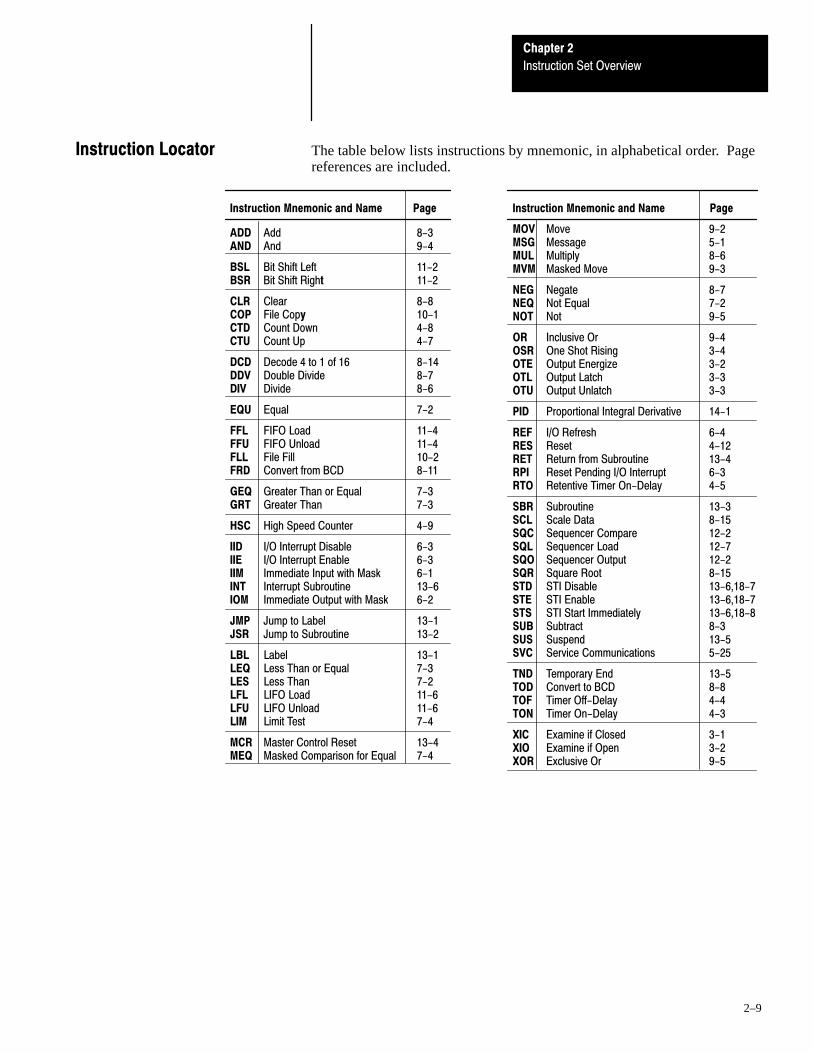
Chapter 2
Instruction Set Overview
2–9
The table below lists instructions by mnemonic, in alphabetical order. Pagereferences are included.
PagePage Instruction Mnemonic and Name
MOV Move 9-2MSG Message 5-1MUL Multiply 8-6MVM Masked Move 9-3
NEG Negate 8-7NEQ Not Equal 7-2NOT Not 9-5
OR Inclusive Or 9-4OSR One Shot Rising 3-4OTE Output Energize 3-2OTL Output Latch 3-3OTU Output Unlatch 3-3
PID Proportional Integral Derivative 14-1
REF I/O Refresh 6-4RES Reset 4-12RET Return from Subroutine 13-4RPI Reset Pending I/O Interrupt 6-3RTO Retentive Timer On-Delay 4-5
SBR Subroutine 13-3SCL Scale Data 8-15SQC Sequencer Compare 12-2SQL Sequencer Load 12-7SQO Sequencer Output 12-2SQR Square Root 8-15STD STI Disable 13-6,18-7STE STI Enable 13-6,18-7STS STI Start Immediately 13-6,18-8SUB Subtract 8-3SUS Suspend 13-5SVC Service Communications 5-25
TND Temporary End 13-5TOD Convert to BCD 8-8TOF Timer Off-Delay 4-4TON Timer On-Delay 4-3
XIC Examine if Closed 3-1XIO Examine if Open 3-2XOR Exclusive Or 9-5
Instruction Mnemonic and Name
ADD Add 8-3AND And 9-4
BSL Bit Shift Left 11-2BSR Bit Shift Right 11-2
CLR Clear 8-8COP File Copy 10-1CTD Count Down 4-8CTU Count Up 4-7
DCD Decode 4 to 1 of 16 8-14DDV Double Divide 8-7DIV Divide 8-6
EQU Equal 7-2
FFL FIFO Load 11-4FFU FIFO Unload 11-4FLL File Fill 10-2FRD Convert from BCD 8-11
GEQ Greater Than or Equal 7-3GRT Greater Than 7-3
HSC High Speed Counter 4-9
IID I/O Interrupt Disable 6-3IIE I/O Interrupt Enable 6-3IIM Immediate Input with Mask 6-1INT Interrupt Subroutine 13-6IOM Immediate Output with Mask 6-2
JMP Jump to Label 13-1JSR Jump to Subroutine 13-2
LBL Label 13-1LEQ Less Than or Equal 7-3LES Less Than 7-2LFL LIFO Load 11-6LFU LIFO Unload 11-6LIM Limit Test 7-4
MCR Master Control Reset 13-4MEQ Masked Comparison for Equal 7-4
Instruction Locator
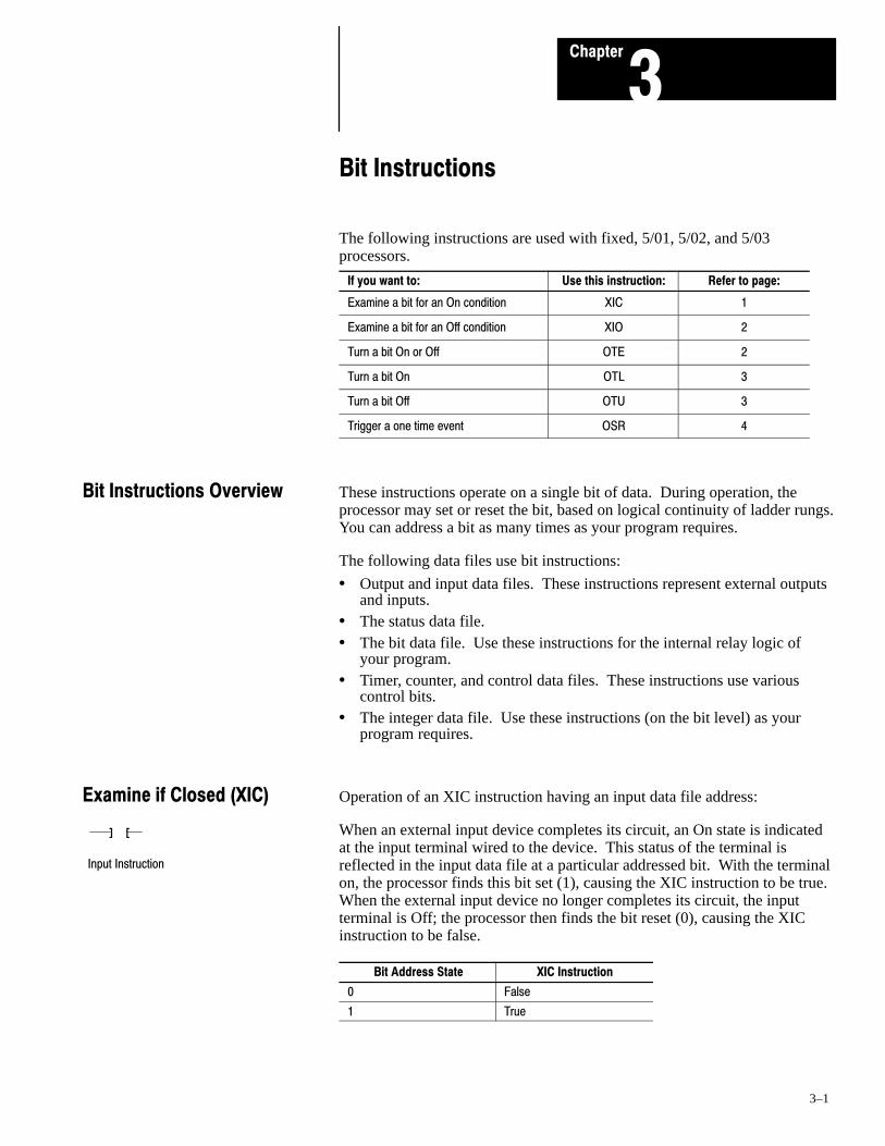
A–B 3Chapter
3–1
Bit Instructions
The following instructions are used with fixed, 5/01, 5/02, and 5/03processors.
If you want to: Use this instruction: Refer to page:
Examine a bit for an On condition XIC 1
Examine a bit for an Off condition XIO 2
Turn a bit On or Off OTE 2
Turn a bit On OTL 3
Turn a bit Off OTU 3
Trigger a one time event OSR 4
These instructions operate on a single bit of data. During operation, theprocessor may set or reset the bit, based on logical continuity of ladder rungs.You can address a bit as many times as your program requires.
The following data files use bit instructions:
• Output and input data files. These instructions represent external outputsand inputs.
• The status data file.• The bit data file. Use these instructions for the internal relay logic of
your program.• Timer, counter, and control data files. These instructions use various
control bits.• The integer data file. Use these instructions (on the bit level) as your
program requires.
Operation of an XIC instruction having an input data file address:
When an external input device completes its circuit, an On state is indicatedat the input terminal wired to the device. This status of the terminal isreflected in the input data file at a particular addressed bit. With the terminalon, the processor finds this bit set (1), causing the XIC instruction to be true.When the external input device no longer completes its circuit, the inputterminal is Off; the processor then finds the bit reset (0), causing the XICinstruction to be false.
Bit Address State XIC Instruction
0 False
1 True
Bit Instructions Overview
] [
Input Instruction
Examine if Closed (XIC)

XIC, XIO, OTE, OTL, OTU, OSR
Chapter 3
Bit Instructions
3–2
Operation of an XIO instruction having an input data file address:
When an external input device does not complete its circuit, an Off state isindicated at the input terminal wired to the device. This status of theterminal is reflected in the input data file at a particular addressed bit. Withthe terminal off, the processor finds this bit in the reset condition (0),meaning the XIO instruction is true. When the external input devicecompletes its circuit, the input terminal will be On; the processor then findsthe bit set (1), meaning the XIO instruction is false.
Bit Address State XIO Instruction
0 True
1 False
Operation of an OTE instruction having an output data file address:
The OTE instruction is a non-retentive output instruction. The status of anoutput terminal is reflected in the output data file at a particular bit address.When the processor finds a true logic path in the rung containing the OTEinstruction, it sets this bit (1); this turns the output terminal On and energizesthe output device wired to the terminal. When a true logic path no longerexists, the processor resets the bit (0), turning the terminal Off andde-energizing the output device.
OTE instructions are reset when:
• You enter or return to the REM Run or REM Test mode or power isrestored.
• The OTE is programmed within an inactive or false Master Control Reset(MCR) zone.
Important: A bit that is set within a subroutine using an OTE instructionremains set until the subroutine is scanned again.
]/[
Input Instruction
Examine if Open (XIO)
( )
Output Instruction
Output Energize (OTE)
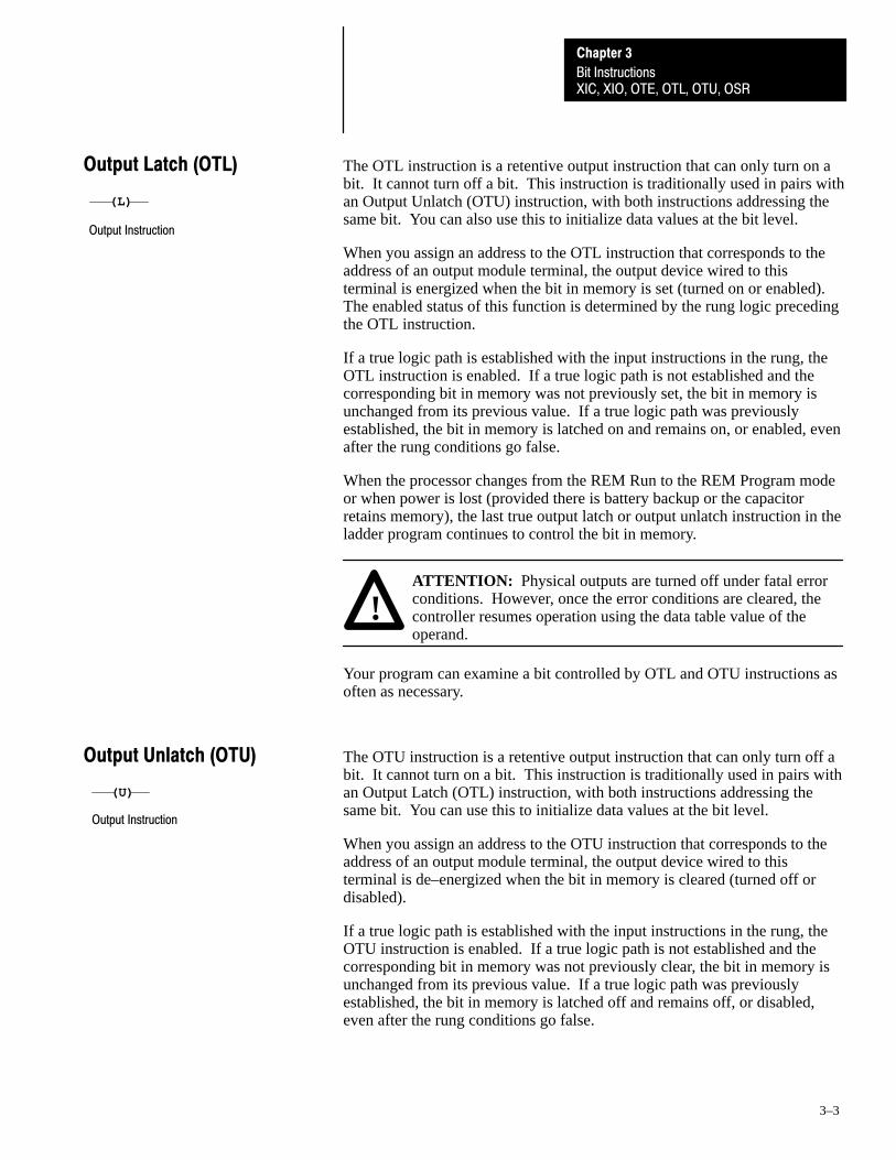
XIC, XIO, OTE, OTL, OTU, OSR
Chapter 3
Bit Instructions
3–3
The OTL instruction is a retentive output instruction that can only turn on abit. It cannot turn off a bit. This instruction is traditionally used in pairs withan Output Unlatch (OTU) instruction, with both instructions addressing thesame bit. You can also use this to initialize data values at the bit level.
When you assign an address to the OTL instruction that corresponds to theaddress of an output module terminal, the output device wired to thisterminal is energized when the bit in memory is set (turned on or enabled).The enabled status of this function is determined by the rung logic precedingthe OTL instruction.
If a true logic path is established with the input instructions in the rung, theOTL instruction is enabled. If a true logic path is not established and thecorresponding bit in memory was not previously set, the bit in memory isunchanged from its previous value. If a true logic path was previouslyestablished, the bit in memory is latched on and remains on, or enabled, evenafter the rung conditions go false.
When the processor changes from the REM Run to the REM Program modeor when power is lost (provided there is battery backup or the capacitorretains memory), the last true output latch or output unlatch instruction in theladder program continues to control the bit in memory.
!ATTENTION: Physical outputs are turned off under fatal errorconditions. However, once the error conditions are cleared, thecontroller resumes operation using the data table value of theoperand.
Your program can examine a bit controlled by OTL and OTU instructions asoften as necessary.
The OTU instruction is a retentive output instruction that can only turn off abit. It cannot turn on a bit. This instruction is traditionally used in pairs withan Output Latch (OTL) instruction, with both instructions addressing thesame bit. You can use this to initialize data values at the bit level.
When you assign an address to the OTU instruction that corresponds to theaddress of an output module terminal, the output device wired to thisterminal is de–energized when the bit in memory is cleared (turned off ordisabled).
If a true logic path is established with the input instructions in the rung, theOTU instruction is enabled. If a true logic path is not established and thecorresponding bit in memory was not previously clear, the bit in memory isunchanged from its previous value. If a true logic path was previouslyestablished, the bit in memory is latched off and remains off, or disabled,even after the rung conditions go false.
(L)
Output Instruction
Output Latch (OTL)
(U)
Output Instruction
Output Unlatch (OTU)

XIC, XIO, OTE, OTL, OTU, OSR
Chapter 3
Bit Instructions
3–4
When the processor changes from the REM Run to the REM Program modeor when power is lost (provided there is battery backup or the capacitorretains memory), the last true output latch or output unlatch instruction in theladder program continues to control the bit in memory.
!ATTENTION: Physical outputs are turned off under fatal errorconditions. However, once the error conditions are cleared, thecontroller resumes operation using the data table value of theoperand.
Your program can examine a bit controlled by OTL and OTU instructions asoften as necessary.
The OSR instruction is a retentive input instruction that triggers an event tooccur one time. Use the OSR instruction when an event must start based onthe change of state of the rung from false to true, not on the resulting status.Applications include starting events triggered by a pushbutton switch. Anexample is freezing rapidly displayed LED values.
Instruction Parameters
The address assigned to the OSR instruction is not the one shot addressreferenced by your program. This address allows the OSR instruction toremember its previous rung state. The output instruction(s) that follow theOSR instruction can be referenced by your program as the “1 shot.”
Use a bit address from either the bit or integer data file. The addressed bit isset (1) as long as rung conditions preceding the OSR instruction are true; thebit is reset (0) when rung conditions preceding the OSR instruction are false.
The bit address you use for this instruction must be unique. Do not use itelsewhere in the program.
We recommend that you do not use an input or output address to program theaddress parameter of the OSR instruction.
Examples
The following rungs illustrate the use of the OSR instruction. The first tworungs apply to 5/01, 5/02, and 5/03 processors. The third rung involvesoutput branching and applies to the 5/02 and 5/03 processors only.
[OSR]
Input Instruction
One-Shot Rising (OSR)
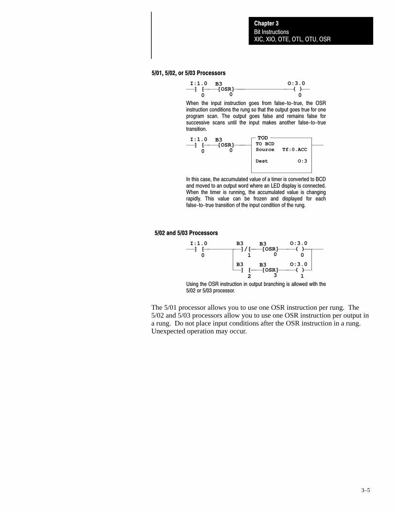
XIC, XIO, OTE, OTL, OTU, OSR
Chapter 3
Bit Instructions
3–5
( )O:3.0
0]/[
B3
1
TODTO BCDSource Tf:0.ACC
Dest O:3
When the input instruction goes from false-to-true, the OSRinstruction conditions the rung so that the output goes true for oneprogram scan. The output goes false and remains false forsuccessive scans until the input makes another false-to-truetransition.
5/01, 5/02, or 5/03 Processors
] [I:1.0
0[OSR]
B3
0( )
O:3.0
0
[OSR]B3
3( )
O:3.0
1] [
B3
2
] [I:1.0
0[OSR]
B3
0
] [I:1.0
0[OSR]
B3
0
5/02 and 5/03 Processors
In this case, the accumulated value of a timer is converted to BCDand moved to an output word where an LED display is connected.When the timer is running, the accumulated value is changingrapidly. This value can be frozen and displayed for eachfalse-to-true transition of the input condition of the rung.
Using the OSR instruction in output branching is allowed with the5/02 or 5/03 processor.
The 5/01 processor allows you to use one OSR instruction per rung. The5/02 and 5/03 processors allow you to use one OSR instruction per output ina rung. Do not place input conditions after the OSR instruction in a rung.Unexpected operation may occur.
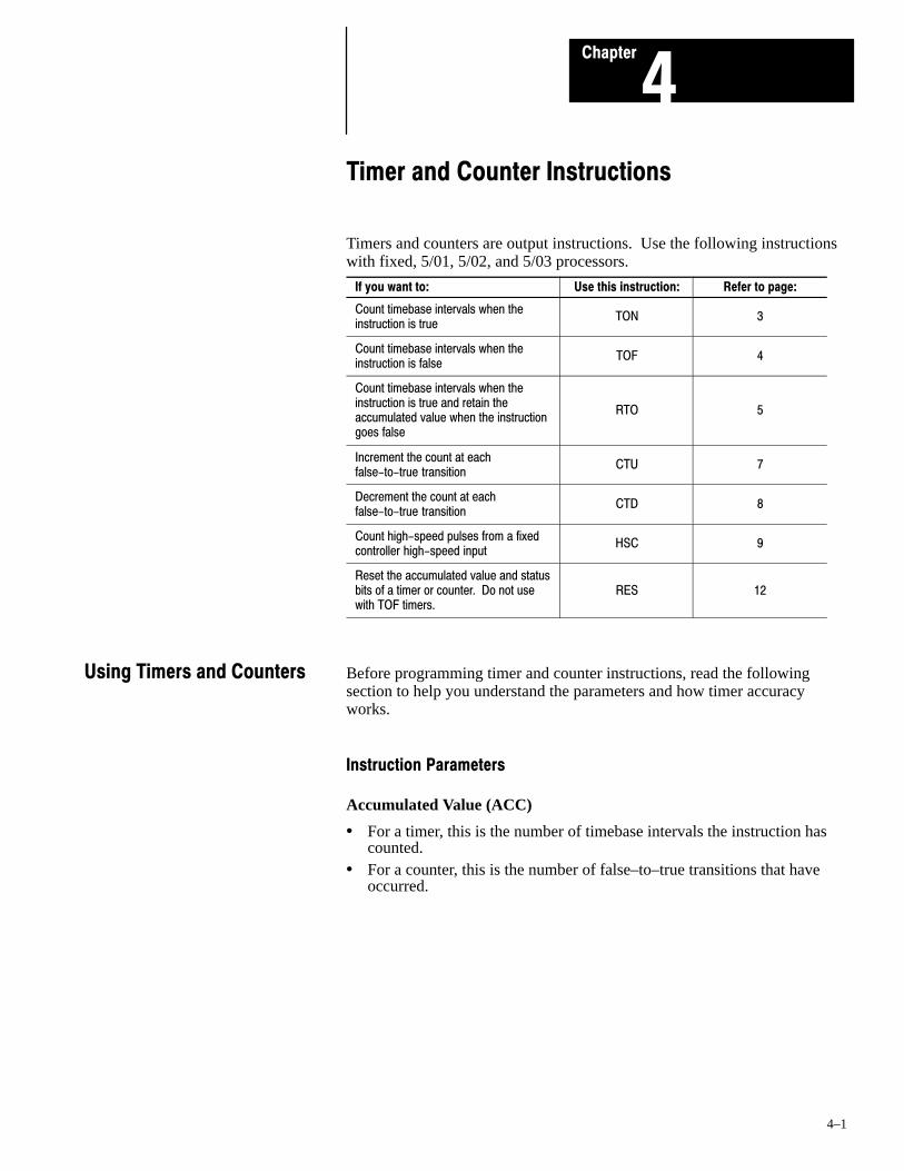
A–B 4Chapter
4–1
Timer and Counter Instructions
Timers and counters are output instructions. Use the following instructionswith fixed, 5/01, 5/02, and 5/03 processors.
If you want to: Use this instruction: Refer to page:
Count timebase intervals when theinstruction is true
TON 3
Count timebase intervals when theinstruction is false
TOF 4
Count timebase intervals when theinstruction is true and retain theaccumulated value when the instructiongoes false
RTO 5
Increment the count at eachfalse-to-true transition
CTU 7
Decrement the count at eachfalse-to-true transition
CTD 8
Count high-speed pulses from a fixedcontroller high-speed input
HSC 9
Reset the accumulated value and statusbits of a timer or counter. Do not usewith TOF timers.
RES 12
Before programming timer and counter instructions, read the followingsection to help you understand the parameters and how timer accuracyworks.
Instruction Parameters
Accumulated Value (ACC)
• For a timer, this is the number of timebase intervals the instruction hascounted.
• For a counter, this is the number of false–to–true transitions that haveoccurred.
Using Timers and Counters

CTU, CTD, HSC, RES
Chapter 4
Timer and Counter Instructions TON, TOF, RTO,
4–2
Preset Value (PRE)
The preset value is the set point that you enter in the timer or counterinstruction. When the accumulated value becomes equal to or greater thanthe preset value, the done status bit is set. You can use this bit to control anoutput device.
• Preset and accumulated values for timers range from 0 to +32,767. If atimer preset or accumulated value is a negative number, a runtime erroroccurs and places the processor in a fault condition.
• Preset and accumulated values for counters range from –32,768 to+32,767.
Timebase
The timebase determines the duration of each timebase interval. For fixedand 5/01 processors, the timebase is set at 0.01 second. For 5/02 and 5/03processors the timebase is selectable as 0.01 second or 1.0 second.
Timer Accuracy
Timer accuracy refers to the length of time between the moment a timerinstruction is enabled and the moment the timed interval is complete.Inaccuracy caused by the program scan can be greater than the timertimebase. You must also consider the time required to energize the outputdevice.
Timing accuracy is −0.01 to +0 seconds, with a program scan of up to 2.5seconds.
Timing could be inaccurate if Jump (JMP), Label (LBL), Jump to Subroutine(JSR), or Subroutine (SBR) instructions skip over the rung containing a timerinstruction while the timer is timing. If the skip duration is within 2.5seconds, no time will be lost; if the skip duration exceeds 2.5 seconds, anundetectable timing error occurs. When using subroutines, a timer must beexecuted at least every 2.5 seconds to prevent a timing error.
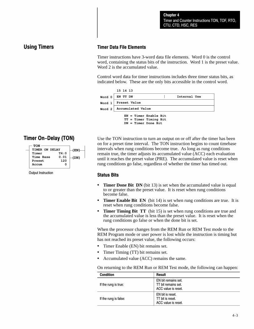
CTU, CTD, HSC, RES
Chapter 4
Timer and Counter Instructions TON, TOF, RTO,
4–3
Timer Data File Elements
Timer instructions have 3-word data file elements. Word 0 is the controlword, containing the status bits of the instruction. Word 1 is the preset value.Word 2 is the accumulated value.
Control word data for timer instructions includes three timer status bits, asindicated below. These are the only bits accessible in the control word.
EN TT DN Internal Use
15 14 13
Preset Value
Accumulated Value
EN = Timer Enable BitTT = Timer Timing BitDN = Timer Done Bit
Word 0
Word 1
Word 2
Use the TON instruction to turn an output on or off after the timer has beenon for a preset time interval. The TON instruction begins to count timebaseintervals when rung conditions become true. As long as rung conditionsremain true, the timer adjusts its accumulated value (ACC) each evaluationuntil it reaches the preset value (PRE). The accumulated value is reset whenrung conditions go false, regardless of whether the timer has timed out.
Status Bits
• Timer Done Bit DN (bit 13) is set when the accumulated value is equalto or greater than the preset value. It is reset when rung conditionsbecome false.
• Timer Enable Bit EN (bit 14) is set when rung conditions are true. It isreset when rung conditions become false.
• Timer Timing Bit TT (bit 15) is set when rung conditions are true andthe accumulated value is less than the preset value. It is reset when therung conditions go false or when the done bit is set.
When the processor changes from the REM Run or REM Test mode to theREM Program mode or user power is lost while the instruction is timing buthas not reached its preset value, the following occurs:
• Timer Enable (EN) bit remains set.• Timer Timing (TT) bit remains set.• Accumulated value (ACC) remains the same.
On returning to the REM Run or REM Test mode, the following can happen:
Condition Result
If the rung is true:EN bit remains set.TT bit remains set.ACC value is reset.
If the rung is false:EN bit is reset.TT bit is reset.ACC value is reset.
Using Timers
(EN)
(DN)
TONTIMER ON DELAYTimer T4:0Time Base 0.01Preset 120Accum 0
Output Instruction
Timer On-Delay (TON)

CTU, CTD, HSC, RES
Chapter 4
Timer and Counter Instructions TON, TOF, RTO,
4–4
Use the TOF instruction to turn an output on or off after its rung has been offfor a preset time interval. The TOF instruction begins to count timebaseintervals when the rung makes a true–to–false transition. As long as rungconditions remain false, the timer increments its accumulated value (ACC)each scan until it reaches the preset value (PRE). The accumulated value isreset when rung conditions go true regardless of whether the timer has timedout.
Status Bits
• Timer Done Bit DN (bit 13) is reset when the accumulated value isgreater than or equal to the preset value. It is set when rung conditionsare true.
• Timer Timing Bit TT (bit 14) is set when rung conditions are false andthe accumulated value is less than the preset value. It is reset when therung conditions go true or when the done bit is reset.
• Timer Enable Bit EN (bit 15) is set when rung conditions are true. It isreset when rung conditions become false.
When processor operation changes from the REM Run or REM Test mode tothe REM Program mode or user power is lost while a timer off-delayinstruction is timing but has not reached its preset value, the followingoccurs:
• Timer Enable (EN) bit remains set.• Timer Timing (TT) bit remains set.• Timer Done (DN) bit remains set.• Accumulated value (ACC) remains the same.
On returning to the REM Run or REM Test mode, the following can happen:
Condition Result
If the rung is true:
TT bit is reset.DN bit remains set.EN bit is set.ACC value is reset.
If the rung is false:
TT bit is reset.DN bit is reset.EN bit is reset.ACC value is set equal to the preset value.
Important: The counter or timer Reset (RES) instruction cannot be usedwith the TOF instruction because RES always clears the statusbits as well as the accumulated value.The TOF times inside an inactive MCR Pair.
(EN)
(DN)
TOFTIMER OFF DELAYTimer T4:1Time Base 0.01Preset 120Accum 0
Output Instruction
Timer Off-Delay (TOF)

CTU, CTD, HSC, RES
Chapter 4
Timer and Counter Instructions TON, TOF, RTO,
4–5
Use the RTO instruction to turn an output on or off after its timer has been onfor a preset time interval. The RTO instruction is a retentive instruction thatbegins to count timebase intervals when rung conditions become true. Aslong as rung conditions remain true, the timer increments its accumulatedvalue (ACC) until it reaches the preset value (PRE).
The RTO instruction retains its accumulated value when any of the followingoccurs:
• Rung conditions become false.• You change processor operation from the REM Run or REM Test mode to
the REM Program mode.• The processor loses power (provided that battery backup is maintained).• A fault occurs.
When you return the processor to the REM Run or REM Test mode and/orrung conditions go true, timing continues from the retained accumulatedvalue. By retaining its accumulated value, retentive timers measure thecumulative period during which rung conditions are true.
Status Bits
• Done Bit DN (bit 13) is set when the accumulated value is greater thanor equal to the preset value. However, it is not reset when rung conditionsbecome false; it is reset only when the appropriate RES instruction isenabled.
• Timer Timing TT (bit 14) is set when rung conditions are true and theaccumulated value is less than the preset value. It is reset when rungconditions go false or when the done bit is set.
• Timer Enable EN (bit 15) is set when rung conditions are true; it isreset when rung conditions are false.
The accumulated value can be reset by the RES instruction. When the RESinstruction having the same address as the RTO is enabled, the accumulatedvalue and the control bits are reset.
When the processor changes from the REM Run or REM Test mode to theREM Program or REM Fault mode, or user power is lost while the timer istiming but not yet at the preset value, the following occurs:
• Timer Enable (EN) bit remains set.• Timer Timing (TT) bit remains set.• Accumulated value (ACC) remains the same.
On returning to the REM Run or REM Test mode or when power is restored,the following can happen:
Condition Result
If the rung is true:TT bit remains set.EN bit remains set.ACC value remains the same and resumes incrementing.
If the rung is false:
TT bit is reset.DN bit remains in its last state.EN bit is reset.ACC value remains in its last state.
(EN)
(DN)
RTORETENTIVE TIMER ONTimer T4:2Time Base 0.01Preset 120Accum 0
Output Instruction
Retentive Timer (RTO)

CTU, CTD, HSC, RES
Chapter 4
Timer and Counter Instructions TON, TOF, RTO,
4–6
Counter Data File Elements
Counter instructions have 3-word data file elements. Word 0 is the controlword, containing the status bits of the instruction. Word 1 is the preset value.Word 2 is the accumulated value.
The control word for counter instructions includes six status bits, as indicatedbelow.
CU CD DN OV UN UA Not Used
15 14 13 12 11 10 09 08 07 06 05 04 03 02 01 00
Preset Value
Accumulated Value
CU = Counter up enable bitCD = Counter down enable bitDN = Done bitOV = Overflow bitUN = Underflow bitUA = Update accumulator (HSC only)
Word 0
Word 1
Word 2
Counter preset and accumulated values are stored as signed integers.Negative values are stored in two’s complementary form.
How Counters Work
The figure below demonstrates how a counter works. The count value mustremain in the range of −32768 to +32767. If the count value goes above+32767 or below −32768, a counter status overflow (OV) or underflow (UN)bit is set.
A counter can be reset to zero using the reset (RES) instruction.
Underflow Overflow
-32,768 +32,767
Count Up
0
Count Down
Counter Accumulator Value
(CTU)
(CTD)
Using Counters

CTU, CTD, HSC, RES
Chapter 4
Timer and Counter Instructions TON, TOF, RTO,
4–7
The CTU is a retentive output instruction that counts false-to-true rungtransitions. Rung transitions can be caused by events occurring in theprogram such as parts traveling past a detector or actuating a limit switch.
Each count is retained when the rung conditions again become false. Thecount is retained until a Reset (RES) instruction having the same address asthe counter instruction is enabled, or until another instruction in yourprogram overwrites the value.
When rung conditions for a CTU instruction have made a false-to-truetransition, the accumulated value is incremented by one count, provided thatthe CTU instruction is evaluated between these transitions.
Status Bits
• Count Up Overflow Bit OV (bit 12) is set when the accumulated valuewraps around to −32,768 (from +32,767) and continues counting up fromthere.
• Done Bit DN (bit 13) is set when the accumulated value equals orexceeds the preset value.
• Count Up Enable Bit CU (bit 15) is set when rung conditions of theCTU instruction are true. The bit is reset when either rung conditions gofalse or an RES instruction having the same address as the CTUinstruction is enabled.
CTU instructions can count beyond their preset value. When countingcontinues past the preset value and reaches (32,767 + 1), an overflowcondition results. This is indicated when the overflow (OV) bit is set. Youcan reset the overflow bit by enabling an RES instruction having the sameaddress as the CTU instruction. You can also reset the overflow bit bydecrementing the count less than or equal to 32,767 with a CTD instruction.
The accumulated value is retained after the CTU or CTD instruction goesfalse, and when power is removed from and then restored to the processor.Also, the on or off status of counter done, overflow, and underflow bits isretentive. The accumulated value and control bits are reset when theappropriate RES instruction is enabled. The CU and CD bits are always setprior to entering the REM Run or REM Test modes.
(CU)
(DN)
CTUCOUNT UPCounter C5:0Preset 120Accum 0
Output Instruction
Count Up (CTU)

CTU, CTD, HSC, RES
Chapter 4
Timer and Counter Instructions TON, TOF, RTO,
4–8
The CTD is a retentive output instruction that counts false-to-true rungtransitions. Rung transitions can be caused by events occurring in theprogram such as parts traveling past a detector or actuating a limit switch.
Each count is retained when the rung conditions again become false. Thecount is retained until a Reset (RES) instruction having the same address asthe counter instruction is enabled, or until another instruction in yourprogram overwrites the value.
When rung conditions for a CTD instruction have made a false-to-truetransition, the accumulated value is decremented by one count.
Status Bits
• Count Down Underflow Bit UN (bit 11) is set when the accumulatedvalue exceeds the lower limit of −32,768 and has wrapped around to+32,767. The CTD instruction continues counting down from there.
• Done Bit DN (bit 13) is reset when the ACC value becomes less thanthe preset. Otherwise the bit is set.
• Count Down Enable CD (bit 14) is set when rung conditions of theCTD instruction are true. It is reset when either rung conditions go false(count down instruction disabled) or the appropriate reset instruction isenabled.
When a CTD instruction counts beyond its preset value and reaches–32,768 − 1, the underflow bit (bit 11) is set. The counter will indicate32,767 and continue decrementing from there. You can reset it by energizingthe appropriate RES instruction. You can also reset the underflow bit byincrementing the count greater than or equal to −32,768 with a CTUinstruction having the same address as the CTD instruction.
The accumulated value is retained after the CTU or CTD instruction goesfalse, and when power is removed from and then restored to the processor.Also, the on or off status of counter done, overflow, and underflow bits isretentive. The accumulated value and control bits are reset when theappropriate RES instruction is enabled.
(CD)
(DN)
CTDCOUNT DOWNCounter C5:1Preset 120Accum 0
Output Instruction
Count Down (CTD)

CTU, CTD, HSC, RES
Chapter 4
Timer and Counter Instructions TON, TOF, RTO,
4–9
The High–Speed Counter is a variation of the CTU counter. The HSCinstruction is enabled when the rung logic is true and disabled when the runglogic is false.
Important: The HSC instruction counts transitions that occur at inputterminal I:0/0. The HSC instruction does not count rungtransitions. You enable or disable the HSC rung to allow ordisallow the counting of transitions occurring at input terminalI:0/0. We recommend placing the HSC instruction in anunconditional rung. Do not place the XIC instruction withaddress I:0/0 in series with the HSC instruction because countsmay be lossed.
The HSC is a special CTU counter for use with 24 VDC 5/01 fixed I/Ocontrollers. The HSC’s status bits and accumulator values are non-retentive.
Important: This instruction provides high speed counting for fixed I/Ocontrollers with 24 VDC Inputs. One HSC instruction isallowed per controller. To use the instruction, you must clip ajumper as described in the Installation and Operation Manualfor Modular Hardware Style Programmable Controllers,Catalog Number 1747–NI002. Input I:0/0 then operates in thehigh speed mode. The address of the high–speed counter enablebit is C5:0/CU. When rung conditions are true, C5:0/CU is setand transitions occurring at input I:0/0 are counted.
To begin high–speed counting, load a preset value into C5:0.PRE and enablethe counter rung. To load a preset value do one of the following:
• change to the REM Run or REM Test mode from another mode• power up the processor in the REM Run mode• reset the HSC using the RES instruction
Automatic reloading occurs when the HSC itself sets the DN bit on interrupt.
Each input transition that occurs at input I:0/0 causes the HSC accumulatorto increment. When the accumulator value equals the preset value, the Donebit (C5:0/DN) is set, the accumulator is cleared, and the preset value(C5:0.PRE) is loaded into the HSC in preparation for the next high–speedtransition at input I:0/0.
Your ladder program should poll the Done bit (C5:0/DN) to determine thestate of the HSC. Once the Done bit has been detected as set, the ladderprogram should clear bit C5:0/DN (using the unlatch OTU instruction)before the HSC accumulator again reaches the preset value, or the overflowbit (C5:0/OV) will be set.The HSC differs from the CTU and CTD counters. The CTU and CTD aresoftware counters. The HSC is a hardware counter and operatesasynchronously to the ladder program scan. The HSC accumulator value(C5:0.ACC) is normally updated each time the HSC rung is evaluated in theladder program. This means that the HSC hardware accumulator value istransferred to the HSC software accumulator. Only use the OTE instructionto transfer this value. The HSC instruction immediately clears bit C5:0/UAfollowing the accumulator update.
(CU)
(DN)
HSCHIGH SPEED COUNTERCounter C5:0Preset 120Accum 0
Output Instruction
High-Speed Counter (HSC)
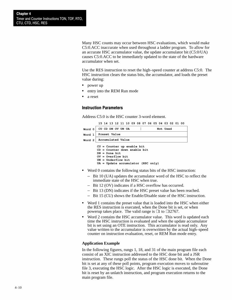
CTU, CTD, HSC, RES
Chapter 4
Timer and Counter Instructions TON, TOF, RTO,
4–10
Many HSC counts may occur between HSC evaluations, which would makeC5:0.ACC inaccurate when used throughout a ladder program. To allow foran accurate HSC accumulator value, the update accumulator bit (C5:0/UA)causes C5:0.ACC to be immediately updated to the state of the hardwareaccumulator when set.
Use the RES instruction to reset the high–speed counter at address C5:0. TheHSC instruction clears the status bits, the accumulator, and loads the presetvalue during:
• power up• entry into the REM Run mode• a reset
Instruction Parameters
Address C5:0 is the HSC counter 3-word element.
CU CD DN OV UN UA Not Used
15 14 13 12 11 10 09 08 07 06 05 04 03 02 01 00
Preset Value
Accumulated Value
CU = Counter up enable bitCD = Counter down enable bitDN = Done bitOV = Overflow bitUN = Underflow bitUA = Update accumulator (HSC only)
Word 0
Word 1
Word 2
• Word 0 contains the following status bits of the HSC instruction:– Bit 10 (UA) updates the accumulator word of the HSC to reflect the
immediate state of the HSC when true.– Bit 12 (OV) indicates if a HSC overflow has occurred.– Bit 13 (DN) indicates if the HSC preset value has been reached.– Bit 15 (CU) shows the Enable/Disable state of the HSC instruction.
• Word 1 contains the preset value that is loaded into the HSC when eitherthe RES instruction is executed, when the Done bit is set, or whenpowerup takes place. The valid range is +1 to +32767.
• Word 2 contains the HSC accumulator value. This word is updated eachtime the HSC instruction is evaluated and when the update accumulatorbit is set using an OTE instruction. This accumulator is read only. Anyvalue written to the accumulator is overwritten by the actual high–speedcounter on instruction evaluation, reset, or REM Run mode entry.
Application Example
In the following figures, rungs 1, 18, and 31 of the main program file eachconsist of an XIC instruction addressed to the HSC done bit and a JSRinstruction. These rungs poll the status of the HSC done bit. When the Donebit is set at any of these poll points, program execution moves to subroutinefile 3, executing the HSC logic. After the HSC logic is executed, the Donebit is reset by an unlatch instruction, and program execution returns to themain program file.
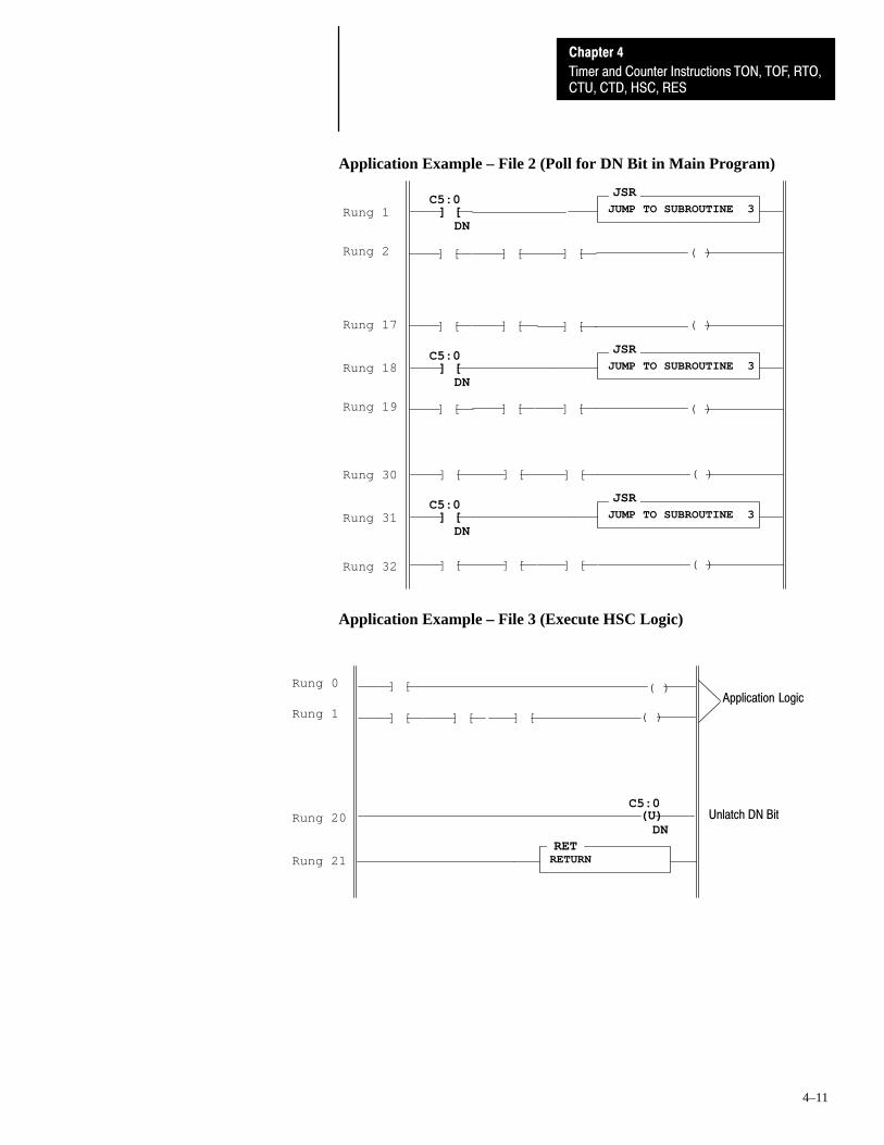
CTU, CTD, HSC, RES
Chapter 4
Timer and Counter Instructions TON, TOF, RTO,
4–11
Application Example – File 2 (Poll for DN Bit in Main Program)
] [C5:0
DN
JUMP TO SUBROUTINE 3Rung 1
Rung 2
Rung 18 ] [C5:0
DN
Rung 17
Rung 19
Rung 30
Rung 31
Rung 32
] [C5:0
DN
JSR
JUMP TO SUBROUTINE 3
JSR
JUMP TO SUBROUTINE 3
JSR
] [ ] [ ] [ ( )
] [ ] [ ] [ ( )
] [ ] [ ] [ ( )
] [ ] [ ] [ ( )
] [ ] [ ] [ ( )
Application Example – File 3 (Execute HSC Logic)
RETRETURN
(U)C5:0
DN
] [
Rung 1
Rung 20
Rung 21
Rung 0 ( )
] [ ] [ ] [ ( )
Application Logic
Unlatch DN Bit
CTU, CTD, HSC, RES
Chapter 4
Timer and Counter Instructions TON, TOF, RTO,
4–12
Use a RES instruction to reset a timer or counter. When the RES instructionis enabled, it resets the retentive on-delay timer, count up, or count downinstruction having the same address as the RES instruction.
Using a RES instruction for a: The processor resets the:
Timer(Do not use a RES instruction with a TOF.)
ACC value to 0DN bitTT bitEN bit
Counter
ACC value to 0OV bitUN bitDN bitCU bitCD bit
Control
POS value to 0EN bitEU bitDN bitEM bitER bitUL bitIN and FD go to last state
If the counter rung is enabled, the CU or CD bit is reset as long as the RESinstruction is enabled.
If the counter preset value is negative, the RES instruction sets theaccumulated value to zero. This in turn causes the done bit to be set by acount down or count up instruction.
!ATTENTION: Because the RES instruction resets theaccumulated value, and the done, timing, and enabled bits, do notuse the RES instruction to reset a TOF instruction. Unpredictablemachine operation or injury to personnel may occur.
(RES)
Output Instruction
Reset (RES)

A–B 5Chapter
5–1
Communication Instructions
This chapter describes the Message (MSG) and Service Communication(SVC) instructions.
Using a 5/02 Processor
The data associated with a message write instruction is not sent when youenable the instruction. Rather, it is sent at the end of the scan or at the time aService Communication (SVC) or Refresh (REF) instruction in your ladderprogram is enabled. In some instances, this means that you must buffer datain your application.
Using a 5/03 Processor
The data associated with a message write instruction is buffered when youenable the instruction (providing that there is space in one of the fourtransmit buffers).
Message Instruction (5/02 Only)
This is an output instruction that allows you to transfer data from one node toanother via the DH–485 network.
The instruction can be programmed as a write or read message. The targetdevice can be another SLC 500 processor on the network, or a non-SLC 500device, using the common interface file (485CIF file 9 in SLC 500processors). The 485CIF protocol is also used for PLC2 type messages.
When you select the SLC500 as your target device, communication can takeplace between:
• a 5/02 processor and any other SLC 500 family processor• a 5/03 processor and any other SLC 500 family processor
The message instruction cannot be programmed in the fixed or 5/01processor.
Communication InstructionsOverview

Chapter 5
Communication Instructions
5–2
The 5/02 processor can service one message instruction at any given time,although the processor may hold several messages “enabled and waiting.”Waiting messages are serviced one at a time in sequential order (first in firstout).
Related Status File Bits
Three status file bits are related to the MSG instruction:
• Bit S:2/5 DH–485 Incoming Command Pending – Read only. This bit isset when the processor determines that another node on the DH–485network has requested information or supplied a command to it. This bitcan become set at any time. This bit is cleared when the processorservices the request (or command).Use this bit as a condition of an SVC instruction to enhance thecommunication capability of your processor.
• Bit S:2/6 DH–485 Message Reply Pending – Read only. This bit is setwhen another node on the DH–485 network has supplied the informationthat you requested in the MSG instruction of your processor. This bit iscleared when the processor stores the information and updates your MSGinstruction.Use this bit as a condition of an SVC instruction to enhance thecommunication capability of your processor.
• Bit S:2/7 DH–485 Outgoing Message Command Pending – Read only.This bit is set when one or more messages in your program are enabledand waiting, but no message is being transmitted at the time. As soon astransmission of a message begins, the bit is cleared. After transmission,the bit is set again if there are further messages waiting, or it remainscleared if there are no further messages waiting.Use this bit as a condition of an SVC instruction to enhance thecommunication capability of your processor.
You may also want to use bit S:2/15 DH–485 Communications ServicingSelection. Refer to chapter 1 in this manual for more information.
Available Configuration Options
The following configuration options are available with a 5/02 processor:
• Peer–to–Peer Write on a Local network to another SLC 500 processor• Peer–to–Peer Read on a Local network to another SLC 500 processor
• Peer–to–Peer Write on a Local network to a 485CIF (PLC2 emulation)• Peer–to–Peer Read on a Local network to a 485CIF (PLC2 emulation)
(EN)(DN)(ER)
MSGREAD/WRITE MESSAGERead/writeTarget DeviceControl BlockControl Block Length 7
Output Instruction
Using a 5/02 Processor
Chapter 5
Communication Instructions
5–3
Entering Parameters
After you place the MSG instruction on a rung, specify whether the messageis to be a read or write. Then specify the target device and the control blockfor the MSG instruction.
• Read/Write – Read indicates that the local processor (processor in whichthe instruction is located) is receiving data; write indicates that it issending data.
• Target Device identifies the type of device which will receive data. Validoptions are:– 500CPU, if the target device is another SLC processor– 485CIF, if the target device is a non–SLC device (PLC2 emulator)
• Control Block is an integer file address that you select. It is a 7-elementfile, containing the status bits, target file address, and other dataassociated with the message instruction.
• Control Block Length is fixed at seven elements. This field cannot bealtered.

Chapter 5
Communication Instructions
5–4
Data Entry Screen
After you enter the control block address, the APS software displays thefollowing data entry screen:
Read/Write: READ ignore if timed out: 0 TO Target Device: 500CPU to be retried: 0 NR Control Block: N7:0 awaiting execution: 0 EWF1 Local Destination File Address: ***F2 Target Node: 0 error: 0 ERF3 Target File Address: *** message done: 0 DNF4 Message Length in elements *** message transmitting: 0 ST
message enabled: 0 EN
control bit address: N7:0/8
ERROR CODE: 0 Error Code Desc:
Press a function key, <ENTER> to save and exit, or <ESC> to abort offline no forces INSTR INSERT File 009
Message:Prompt:Data/Cmd Entry:Status:
Main Functions:
F9
TOGGLEBIT
Display Area:
F1 F3 F4F2
DESTADDRESS
TARGETADDRESS
MESSAGELENGTH
TARGETNODE
The left column in this display indicates the entries you’ve made for theRead/Write, Target Device, and Control Block parameters. It also listsfurther parameters (function keys [F1]– [F4]) you must enter.
Function Key Description
[F1] Destination Address
If a Read message instruction, this parameter is the localdestination file address, the address in the local processorwhich is to receive data. If a Write message instruction,this parameter is the local source file address, the addressin the local processor which is to send data. Valid file typesare S, B, T, C, R, N.
[F2] Target NodeThe node number of the processor that is to communicatewith the local processor.
[F3] Target Address
If the target device is a 500CPU, this is the source ordestination file address in the target processor. Valid filetypes are S, B, T, C, R, N. If the target device is 485CIF,this is the offset value in the common interface file.
[F4] Message Length
The length of the message in elements. One wordelements are limited to a maximum length of 1-41. Threeword elements (T, C, R) are limited to a maximum length of1-13.

Chapter 5
Communication Instructions
5–5
Example
The destination file type determines the number of words that are transferred.
• A MSG read instruction specifying a target file type C (counter), adestination file type N (integer), and a length value of 1 transfers 1 wordof information.
• A MSG read instruction specifying a target file type N, a destination filetype C, and a length value of 1 transfers 3 words.
Using Status Bits
The right column of the APS display shown on page 5–4 lists the variousstatus bits associated with the MSG instruction using a 5/02 processor.
Function key [F9], Toggle Bit allows you to change the status of the bits.
• Time Out Bit TO (bit 08) You can set this bit in your application toremove an active message instruction from processor control. Yourapplication must supply its own timeout value. An example appears onpages 5–8 and 5–10.
• No Response Bit NR (bit 09) is set if the target processor does notrespond to the first message request. The NR bit is reset when the ER,DN, or ST bit is set.
• Enabled and Waiting Bit EW (bit 10) is set after the enable bit is setand the message is waiting to be sent.
• Error Bit ER (bit 12) is set when message transmission has failed. TheER bit is reset the next time the associated rung goes from false to true.
• Done Bit DN (bit 13) is set when the message is transmittedsuccessfully. The DN bit is reset the next time the associated rung goesfrom false to true.
• Start Bit ST (bit 14) is set when the processor receivesacknowledgement from the target device. The ST bit is reset when theDN, ER, or TO bit is set.
• Enable Bit EN (bit 15) is set when rung conditions go true and theinstruction is being executed. It remains set until the messagetransmission is complete and the rung goes false.

Chapter 5
Communication Instructions
5–6
The following section describes the timing diagram for a 5/02 MSGinstruction.
Rung goes True. Target nodereceives packet.
Target node processes packetsuccessfully and returns data(read) or writes data (success).
EN
EW
ST
10
10
10
DN
ER
1010
NR10
TO10
➄➀ ➁ ➂
1. When the MSG rung becomes true and the MSG is scanned, the EN bit isset and remains set until either the DN, ER, or TO bit is set. The EW bitis set, indicating that the MSG instruction has been placed in the MSGQueue. (The 5/02 processor always has room in the MSG Queue.) Thequeue works on a first–in–first–out basis that allows the 5/02 processor toremember the order the MSG instructions were enabled. Note that theprogram does not have access to the 5/02 MSG Queue.
2. At the next end of scan or Service Communication instruction (SVC), the5/02 processor determines if it should examine the MSG Queue for“something to do.” The processor bases its decision on the state of bitS:2/15, DH–485 communication requests from other nodes, and if aprevious MSG instruction is already in progress. If the 5/02 processordetermines that it should not access the queue, the EN and EW bitsremain set until the next end of scan or SVC.
If the 5/02 processor determines that it has “something to do” it uses thefirst message queue entry to build a DH–485 packet. If a packet can besuccessfully built, it is placed in the transmit buffer. If a packet cannot besuccessfully built, the ER bit is set and a code is placed in the MSG blockto inform you of the error.
If this were a MSG Write instruction, the source data would be transferredto the transmit buffer at this time.
The 5/02 processor then exits the end of scan or SVC portion of the scan.The processor’s background communication function sends thetransmitted buffer packet to the Target Node that you specified in yourMSG instruction.
Timing Diagram for aSuccessful 5/02 MSGInstruction
Chapter 5
Communication Instructions
5–7
3. If the Target Node successfully receives the DH–485 packet, it sends backan ACK (an acknowledge). The ACK causes the processor to clear theEW bit and set the ST bit. Note that the Target Node has not yetexamined the DH–485 packet to see if it understands your request.
Once the ST bit is set, the processor will wait indefinitely for a reply fromthe Target Node. The Target Node is not required to respond within anygive time frame. At this time, no other MSG instruction will be serviced.
Important: If the Target Node faults or power cycles during this timeframe of a MSG transaction, you will never receive a reply.This why it is recommended you use a timer instruction inconjunction with the TO bit. Refer to the example on page5–12.
Step 4 is not shown in the timing diagram.
4. If you do not receive an ACK, step 3 does not occur. Instead a NAK (noacknowledge) is received. When this happens, the ST bit remains clear.A NAK indicates:
• either the Target Node is not there,• it does not respond• it is too busy, or• it receives a corrupt DH–485 packet.
When a NAK occurs, the EW bit is cleared and the NR bit is set for onescan. The next time the MSG instruction is scanned, the ER bit is set andthe NR bit is cleared. This indicates that the MSG instruction failed.Note that if the Target Node is too busy, the ER bit is not set. Instead, theMSG instruction re–queues itself for re–transmission.
5. Following the successful receipt of the packet, the Target Node sends areply packet. The reply packet will contain one of the followingresponses:
• I have successfully performed your write request.• I have successfully performed your read request, and here is your data.• I have not performed your request, you are in error.
At the next end of scan or SVC, following the Target Node’s reply, the5/02 processor examines the DH–485 packet from the target device. Ifthe reply contains “I have successfully performed your write request,” theDN bit is set and the ST bit is cleared. The MSG instruction function iscomplete. If the MSG rung is false, the EN bit is cleared the next timethe MSG instruction is scanned.
If the reply contains “I have successfully performed your read request,and here is your data,” the data is written to the data table, the DN bit isset and the ST bit is cleared. The MSG instruction function is complete.If the MSG rung is false, the EN bit is cleared the next time the MSGinstruction is scanned.
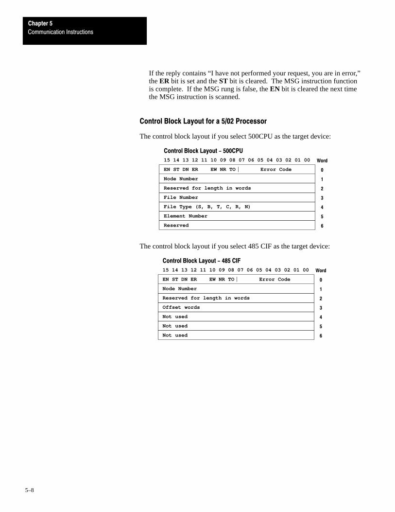
Chapter 5
Communication Instructions
5–8
If the reply contains “I have not performed your request, you are in error,”the ER bit is set and the ST bit is cleared. The MSG instruction functionis complete. If the MSG rung is false, the EN bit is cleared the next timethe MSG instruction is scanned.
Control Block Layout for a 5/02 Processor
The control block layout if you select 500CPU as the target device:
EN ST DN ER EW NR TO Error Code
15 14 13 12 11 10 09 08 07 06 05 04 03 02 01 00
Node Number
Reserved for length in words
Control Block Layout - 500CPU
Word
0
1
2
File Number
File Type (S, B, T, C, R, N)
Element Number
Reserved
3
4
5
6
The control block layout if you select 485 CIF as the target device:
EN ST DN ER EW NR TO Error Code
15 14 13 12 11 10 09 08 07 06 05 04 03 02 01 00
Node Number
Reserved for length in words
Control Block Layout - 485 CIF
Word
0
1
2
Offset words
Not used
Not used
Not used
3
4
5
6

Chapter 5
Communication Instructions
5–9
Application Examples
1. Application example 1 is shown below. It indicates how you canimplement continuous operation of a message instruction.
2. Application example 2 appears on pages 5–10 and 5–11. It involves a5/02 processor and a 5/01 processor communicating on a DH–485network. Interlocking is provided to verify data transfer and to shut downboth processors if communication fails.
Operation: A temperature-sensing device, connected as an input to the5/02 processor, controls the on-off operation of a cooling fan, connectedas an output to the 5/01 processor. The 5/02 and 5/01 ladder programs areexplained in the figure on page 5–11.
3. Application example 3 appears on page 5–12. It shows you how to usethe timeout bit to disable an active message instruction. In this example,an output is energized after five unsuccessful attempts (two secondsduration) to transmit a message.
Example 1
Bit B3/1 enables the MSG instruction. When the MSG instruction done bitis set, it unlatches the MSG enable bit so that the MSG instruction will beenabled in the next scan. This provides continuous operation.
The MSG error bit will also unlatch the enable bit. This provides continuousoperation regardless of errors.
] [B3
1
(U)N7:0
15*
(EN)
(DN)
(ER)
MSGREAD/WRITE MESSAGERead/write WRITETarget Device 500CPUControl Block N7:0Control Block Length 7
END
] [N7:0
13*
] [N7:0
12*
0
1
2
* MSG instruction status bits: 12 = ER 13 = DN 15 = EN
Operation Notes
Chapter 5
Communication Instructions
5–10
Example 2 – Program File 2 of 5/02 Processor
(U) B3
0
(EN)
(DN)
(ER)
MSGREAD/WRITE MESSAGERead/write WRITETarget Device 500CPUControl Block N10:0Control Block Length 7
END
0
2
* MSG instruction status bits: 13 = DN 15 = EN
]/[N7:0
0
(L) B3
0
( )N7:0
1
(RES)T4:0
(EN)
(DN)
TONTIMER ON DELAYTimer T4:0Time Base 0.01Preset 400Accum 0
Temperature-sensingInput Device
] [S:1
15
] [S:4
6
3
] [B3
0
(L)N7:0
0
] [S:1
15
] [I:1.0
5
(EN)
(DN)
(ER)
MSGREAD/WRITE MESSAGERead/write READTarget Device 500CPUControl Block N11:0Control Block Length 7
] [N10:0
13*
] [T4:0
DN
] [N11:0
13*
(U) B3
0
(RES)T4:0
(L)N7:0
0
(U)N11:0
15*
(U)N10:0
15*
Operation notes appear on the following page.
4
5
6
7
Bit 1 of the messageword. Used for fancontrol.
Bit 0 of the messageword. This is theinterlock bit.
4-second Timer
Write message instruction.The source and target fileaddresses are N7:0Target node: 3Message length: 1 word.
Read message instruction.The destination and targetfile addresses are N7:0Target node: 3Message length: 1 word.
Latch - This alarminstruction notifies theapplication if the interlockbit N7:0/0 remains set formore than 4 seconds.
First Pass Bit
First Pass Bit
1280 ms Clock Bit
Message Write DoneBit
Message Read DoneBit
1
(L)B
10

Chapter 5
Communication Instructions
5–11
Example 2 – Program File 2 of 5/01 Processor at Node 3
Operation Notes, 5/02 and 5/01 programs
5/02 processor: N7:0/0 is latched; timer T4:0 is reset; B3/0 isunlatched (rung 1), then latched (rung 3). 5/01 processor: N7:0/0 isunlatched; timer T4:0 is reset.
Message instruction operation: The message write instruction in the5/02 processor is initiated every 1280 ms by clock bit S:4/6. The donebit of the message write instruction initiates the message readinstruction.
B3/0 latches the message write instruction. B3/0 is unlatched when themessage read instruction done bit is set, provided that the interlock bitN7:0/0 is reset.
Communication failure: In the 5/02 processor, bit B3/10 becomes set ifinterlock bit N7:0/0 remains set (1) for more than 4 seconds. In the5/01 processor, bit B3/10 becomes set if interlock bit N7:0/0 remainsset (1) for more than 4 seconds. Your application can detect this event,take appropriate action, then unlatch bit B3/10.
(U) N7:0
0
END
0
2
( )B3
1
(RES)T4:0
(EN)
(DN)
TONTIMER ON DELAYTimer T4:0Time Base 0.01Preset 400Accum 0
] [N7:0
0
] [S:1
15First Pass Bit
[OSR]B3
0
] [T4:0
DN
] [B3
1(U)
N7:0
0
(RES)T4:0
( )O:1.0
0] [
N7:0
1
1
3
4
5
6
Bit 0 of the messageword. This is the interlockbit.
4-second Timer
Latch Instruction - This alarmnotifies the application if theinterlock bit N7:0/0 is not setafter 4 seconds.
O:1/0 energizes coolingfan.
Bit 1 of the messageword. Used for fancontrol.
Message instruction parameters: N7:0 is the message word. It is thetarget file address (5/01 processor) and the local source anddestination addresses (5/02 processor) in the message instructions.
N7:0/0 of the message word is the interlock bit; it is written to the 5/01processor as a 1 (set) and read from the 5/01 processor as a 0 (reset).
N7:0/1 of the message word controls cooling fan operation; it is writtento the 5/01 processor as a 1 (set) if cooling is required or as a 0 (reset)if cooling is not required. It is read from the 5/01 processor as either 1or 0.
Word N7:0 should have a value of 1 or 3 during the message writeexecution. N7:0 should have a value of 0 or 2 during the messageread execution.
Program initialization: The first pass bit S:1/15 initializes the ladderprograms on run mode entry.
(L)B3
10
Chapter 5
Communication Instructions
5–12
Example 3
The timeout bit is latched (rung 4) after a period of 2 seconds. Thisclears the message instruction from processor control on the nextscan. The message instruction is then re�enabled for a second attemptat transmission. After 5 attempts, O:1/0 is latched.
A successful attempt at transmission resets the counter, unlatches O:1/0,and unlatches B3/1.
END
0 [LBL] 1
(EN)(DN)(ER)
MSGREAD/WRITE MESSAGERead/write WRITETarget Device 500CPUControl Block N7:0Control Block Length 7
]/[T4:0
DN(EN)(DN)
TONTIMER ON DELAYTimer T4:0Time Base 0.01Preset 200Accum 0
] [B3
1
(CU)
(DN)
CTUCOUNT UPCounter C5:0Preset 5Accum 0
(JMP) 1
N7:0
8
(RES)C5:0
(L)N7:0
(U) B3
1
(L)O:1.0
0
] [B3
1
] [T4:0
DN
] [C5:0
DN
] [N7:0
13*
1
2
3
5
6
7
* MSG instruction status bits: 8 = TO 13 = DN 15 = EN
2-second timer. Eachattempt at transmission has a2-second duration.
Counter allows 5 attempts.
N7:0/8 is the messageinstruction timeout bit (/TO).
Clear the control word andjump back to rung 0 foranother attempt.
The fifth attempt latchesO0:1/0.
B3/1 is latched to initiatethe message instruction.
] [T4:0
DN
4
] [
Operation Notes
8
CLRCLEARDest N7:0
0
(U)O:1.0
0

Chapter 5
Communication Instructions
5–13
The 5/03 processor services up to four message instructions at one time.This means that four message instructions can be in progress simultaneously.If a MSG instruction has entered one of the four “channel independent”transmission buffers and is waiting to be transmitted, its control block willhave status bits EN and EW set. If more than four MSG instructions areenabled at one time, a “channel dependent” overflow queue is used to storethe MSG instruction header blocks (not the data for a MSG write) from thefifth instruction to the fourteenth.
This instruction, queued in a FIFO order will have control block status bitEN set. If more than 14 MSG instructions are enabled at one time for anyone channel, control block status bit WQ is set, as there may be no roomavailable to currently queue the instruction. This instruction must bere–scanned until space exists in the overflow queue.
When using a 5/03 processor the message instruction:
• either, initiates reads and writes through RS–232 Channel 0 whenconfigured for the following protocols:– DF1 Point to Point– DF1 Slave– DH–485, or
• initiates reads and writes through DH485 Channel 1 link using SLC 500or 485CIF (PLC2 emulation) protocol.
Related Status File Bits
Channel 1 Channel 0
S:2/5 Incoming Command Pending S:33/0 Incoming Command Pending
S:2/6 DH-485 Message Reply Pending S:33/1 Message Reply Pending
S:2/7 DH-485 Outgoing Message Command Pending
S:33/2 Outgoing Message Command Pending
S:2/15 DH-485 Communications Servicing Selection
S:33/5 Communication Servicing Selection
S:33/7 Message Servicing Selection S:33/6 Message Servicing Selection
Refer to chapter 1 in this manual for more information on the above statusfile bits.
(EN)
(DN)
(ER)
MSGREAD/WRITE MESSAGETypeRead/writeTarget DeviceLocal/RemoteControl BlockControl Block Length 12
Output Instruction
Using a 5/03 Processor
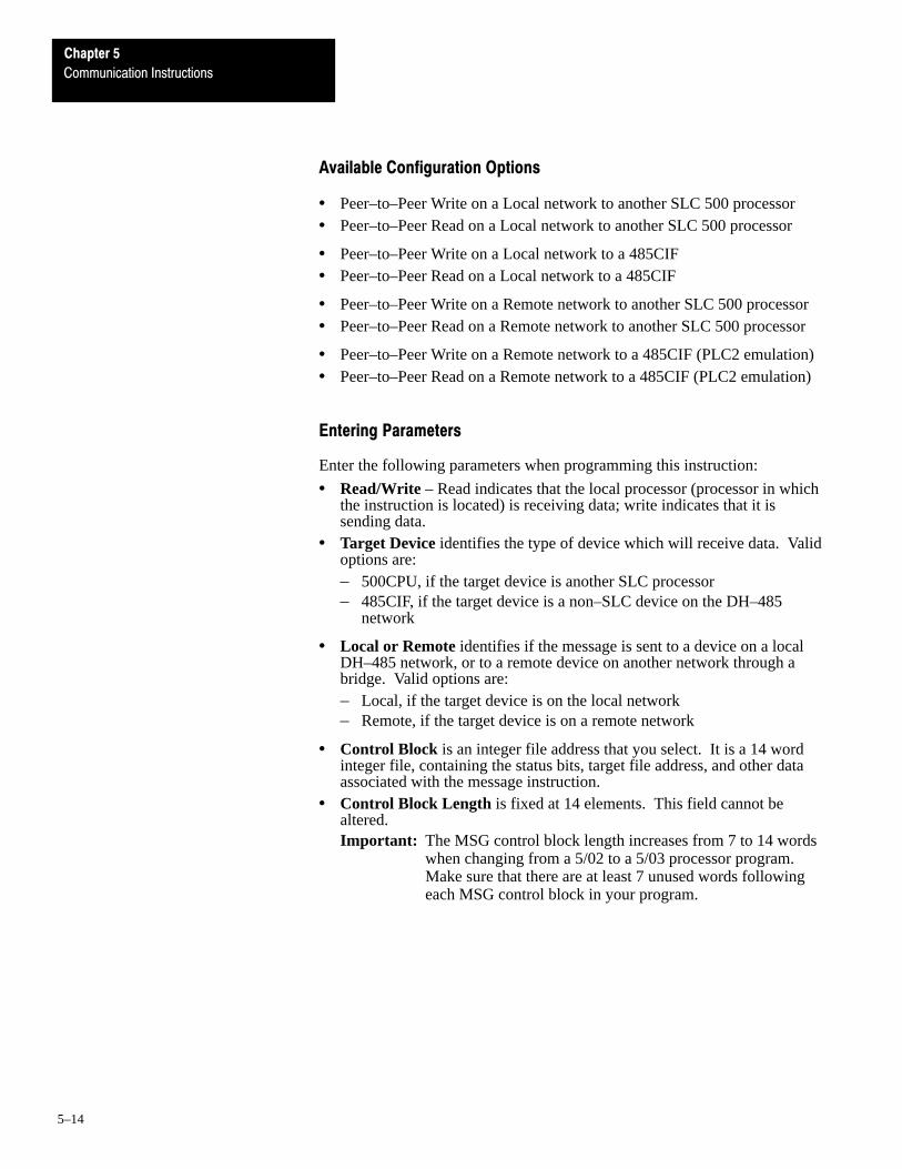
Chapter 5
Communication Instructions
5–14
Available Configuration Options
• Peer–to–Peer Write on a Local network to another SLC 500 processor• Peer–to–Peer Read on a Local network to another SLC 500 processor
• Peer–to–Peer Write on a Local network to a 485CIF• Peer–to–Peer Read on a Local network to a 485CIF
• Peer–to–Peer Write on a Remote network to another SLC 500 processor• Peer–to–Peer Read on a Remote network to another SLC 500 processor
• Peer–to–Peer Write on a Remote network to a 485CIF (PLC2 emulation)• Peer–to–Peer Read on a Remote network to a 485CIF (PLC2 emulation)
Entering Parameters
Enter the following parameters when programming this instruction:
• Read/Write – Read indicates that the local processor (processor in whichthe instruction is located) is receiving data; write indicates that it issending data.
• Target Device identifies the type of device which will receive data. Validoptions are:– 500CPU, if the target device is another SLC processor– 485CIF, if the target device is a non–SLC device on the DH–485
network
• Local or Remote identifies if the message is sent to a device on a localDH–485 network, or to a remote device on another network through abridge. Valid options are:– Local, if the target device is on the local network– Remote, if the target device is on a remote network
• Control Block is an integer file address that you select. It is a 14 wordinteger file, containing the status bits, target file address, and other dataassociated with the message instruction.
• Control Block Length is fixed at 14 elements. This field cannot bealtered.Important: The MSG control block length increases from 7 to 14 words
when changing from a 5/02 to a 5/03 processor program.Make sure that there are at least 7 unused words followingeach MSG control block in your program.

Chapter 5
Communication Instructions
5–15
Using Status Bits
The right column of the APS display shown on the next page lists the variousstatus bits associated with the MSG instruction using a 5/03 processor.
Function key [F9], Toggle Bit allows you to change the status of the bits.
• Time Out Bit TO (bit 08) You can set this bit in your application toremove an active message instruction from processor control. Yourapplication must supply its own timeout logic value if the MSG Timeout(word 7) contains a zero.
• No Response Bit NR (bit 09) is set if the target processor does notrespond to the first message request. The NR bit is reset when the ER,DN, or ST bit is set.
• Enabled and Waiting Bit EW (bit 10) is set after the enable bit is setand the message is buffered and waiting to be sent in the buffer.
• Continuous Operation CO (bit 11) Set this bit if you wish tocontinually send the MSG instruction. If the instruction errors, it willautomatically retry until it is successful. If the instruction is NAKed, itmust be rescanned.
• Error Bit ER (bit 12) is set when message transmission has failed. TheER bit is reset the next time the associated rung goes from false to true.
• Done Bit DN (bit 13) is set when the message is transmittedsuccessfully. The DN bit is reset the next time the associated rung goesfrom false to true.
• Start Bit ST (bit 14) is set when the processor receivesacknowledgement from the target device. The ST bit is reset when theDN, ER, or TO bit is set.
• Enable Bit EN (bit 15) is set when rung conditions go true and theinstruction is being executed. It remains set until message transmission iscompleted and the rung goes false.
• Waiting for Queue Space Bit WQ (Word 7, bit 0) is set when there isno room in the active queue to store write or read data. This bit is clearedwhen space is available in the active queue.
Important: When the WQ bit is set, and you are using a MSG Writeinstruction, your source data is unbuffered. If yourapplication requires buffered (or “snapshot”) data, wait untilthe EW bit is set before overwriting your source data.
• EN = 1 and EW = 1 when MSG gets in the buffer• EN = 1 when MSG gets into queue• WQ = 1 when queue (which holds 10 MSG) is full:
buffer – holds 4 messages with dataqueue – stores pointer (waiting list)
Important: If your program contains four message instructions with theContinuous Operation (CO) bit set, the fault routine’s messageinstruction will not be executed.

Chapter 5
Communication Instructions
5–16
Data Entry Screen
If you select a local read from another 500CPU data table file, the followingscreen appears:
Type: Peer–to–Peer Read/Write: READ ignore if timed out: 0 TO Target Device: 500CPU to be retried: 0 NR Local/Remote: Local awaiting execution: 0 EW Control Block: N10:0 continuous run: 0 COF10 Channel: 1 error: 0 ER F1 Target Node: 2 message done: 0 DN
message transmitting: 0 STmessage enabled: 0 EN
F4 Destination File Addr: N7:0 waiting for queue space: 0 WQ F5 Target Source File Address: N7:50 F6 Message Length In Elements: 10 F7 Message Timeout (seconds): 5 ERROR CODE: 0 control bit address: N10:0/8 Error Code Desc:
Press a function key, <ENTER> to save and exit, or <ESC> to abort offline no forces INSTR INSERT File 009
Message:Prompt:Data/Cmd Entry:Status:
Main Functions:
F9
TOGGLEBIT
Display Area:
F1 F7F5 F6
TARGETNODE
MESSAGELENGTH
FILEADDRESS
TARGETADDRESS
F8
MESSAGETIMEOUT
F10CHANNEL
Function Key Description
[F1] Target NodeSpecifies the node number of the processor that isreceiving the message. Valid range is 0-31. (SpecifiesDH-485 address.)
For a Read (Destination) this is the address in the initiatingprocessor which is to receive data.
[F5] File Address For a Write (Source) this is the address in the initiatingprocessor which is to send data.
Valid file types are S, B, T, C, R, N, I, O, M0, M1.
For a Read (Destination) this is the address in the targetprocessor which is to receive data.
[F6] Target Address For a Write (Source) this is the address in the targetprocessor which is to send data.
Valid file types are S, B, T, C, R, N, I, O, M0, M1.
[F7] Message LengthDefines the length of the message in elements. One wordelements are limited to a maximum length of 1-112. Threeword elements are limited to a maximum length of 1-37.
[F8] Message Timeout
Defines the length of the message timer in seconds. Atimeout of 0 seconds means that there is no timer and themessage will wait indefinitely for a reply. Valid range is0-255 seconds.
[F10] ChannelIdentifies the physical channel used for the messagecommunication. Available channels are (0, RS232) or(1, DH485).
Local Read from a 500CPU

Chapter 5
Communication Instructions
5–17
Monitor Display
The following screen allows you to monitor the status of the messageinstruction while the processor is running:
Type: Peer–to–Peer Read/Write: READ ignore if timed out: 0 TO Target Device: 500CPU to be retried: 0 NR Local/Remote: Local awaiting execution: 0 EW Control Block: N10:0 continuous run: 0 CO Channel: 1 error: 0 ER F1 Target Node: 2 message done: 0 DN
message transmitting: 0 STmessage enabled: 0 EN
Destination File Addr: N7:0 waiting for queue space: 0 WQ F6 Target Source File Address: N7:50 Message Length In Elements: 10 F8 Message Timeout (seconds): 5 ERROR CODE: 0 control bit address: N10:0/8 Error Code Desc:
Press a function key or press <ESC> to exit monitor offline no forces INSTR INSERT File 009
Message:Prompt:Data/Cmd Entry:Status:
Main Functions:
F9
TOGGLEBIT
Display Area:
F1 F6
TARGETNODE
TARGETADDRESS
F8
MESSAGETIMEOUT
In the display above the 5/03 processor reads 10 elements from Target Node2’s N7 file, starting at word N7:50. The 10 words are placed in your integerfile starting at word N7:0. If five seconds elapse without a reply, error bitN10:0/12 will be set, indicating that the instruction timed out. The device atnode 2 understands the SLC500 processor family (500, 5/01, 5/02, and 5/03)protocol.
Chapter 5
Communication Instructions
5–18
Data Entry Screen
If you selected a local read from another 485CIF, the following screenappears:
Type: Peer–to–Peer Read/Write: READ Target Device: 485CIF ignore if timed out: 0 TO Local/Remote: Local to be retried: 0 NR Control Block: N10:0 awaiting execution: 0 EWF10 Channel: 1 continuous run: 0 CO F1 Target Node: 2 error: 0 ER
message done: 0 DNmessage transmitting: 0 ST
message enabled: 0 EN F5 Destination/Source File Addr: N7:0 waiting for queue space: 0 WQ F6 Target Offset: 20 F7 Message Length In Elements: 5 F8 Message Timeout (seconds): 15 ERROR CODE: 0 control bit address: N10:0/8 Error Code Desc:
Press a function key, <ENTER> to save and exit, or <ESC> to abort offline no forces INSTR INSERT File 009
Message:Prompt:Data/Cmd Entry:Status:
Main Functions:
F9
TOGGLEBIT
Display Area:
F1 F7F5 F6
TARGETNODE
MESSAGELENGTH
FILEADDRESS
TARGETOFFSET
F8
MESSAGETIMEOUT
F10CHANNEL
Function Key Description
[F1] Target NodeSpecifies the node number of the processor that isreceiving the message. Valid range is 0-31.
For a Read (Destination) this is the address in the initiatingprocessor which is to receive data.
[F5] File Address For a Write (Source) this is the address in the initiatingprocessor which is to send data.
Valid file types are S, B, T, C, R, N, I, O, M0, M1.
[F6] Target OffsetFor a Read or Write this is the word offset value in thecommon interface file (byte offset for non-SLC device).
[F7] Message LengthDefines the length of the message in elements. One wordelements are limited to a maximum length of 1-112. Threeword elements are limited to a maximum length of 1-37.
[F8] Message Timeout
Defines the length of the message timer in seconds. Atimeout of 0 seconds means that there is no timer and themessage will wait forever for a reply. Valid range is 0-255seconds.
[F10] ChannelIdentifies the physical channel used for the messagecommunication. Available channels are (0, RS232) or(1, DH485).
Local Read from a 485CIF

Chapter 5
Communication Instructions
5–19
Monitor Display
The following screen allows you to monitor the status of the messageinstruction while the processor is running:
Type: Peer–to–Peer Read/Write: READ Target Device: 485CIF ignore if timed out: 0 TO Local/Remote: Local to be retried: 0 NR Control Block: N10:0 awaiting execution: 0 EW Channel: 1 continuous run: 0 CO F1 Node: 2 error: 0 ER
message done: 0 DNmessage transmitting: 0 ST
message enabled: 0 EN Destination/Source File Addr: N7:0 waiting for queue space: 0 WQ F6 Target Offset: 20 Message Length In Elements: 5 F8 Message Timeout (seconds): 15 ERROR CODE: 0 control bit address: N10:0/8 Error Code Desc:
Press a function key or press <ESC> to exit monitor offline no forces INSTR INSERT File 009
Message:Prompt:Data/Cmd Entry:Status:
Main Functions:
F9
TOGGLEBIT
Display Area:
F1 F6
TARGETNODE
TARGETOFFSET
F8
MESSAGETIMEOUT
In the display above the 5/03 processor will read five elements (words) fromTarget Node 2’s CIF file, starting at word 20 (or byte 20 for non–SLC 500devices). The five elements will be placed in your integer file starting atword N7:0. If 15 seconds elapse without a reply, error bit N10:0/12 will beset, indicating that the instruction timed out. The device at node 2understands the 485CIF (PLC2 emulation) protocol.

Chapter 5
Communication Instructions
5–20
Data Entry Screen
The only protocol that supports Remote messaging is DH485. Refer to page5–25 for an illustration of connectivity for remote messaging.
Type: Peer–to–Peer Read/Write: READ Target Device: 500CPU ignore if timed out: 0 TO Local/Remote: Remote to be retried: 0 NR Control Block: N10:0 awaiting execution: 0 EWF10 Channel: 1 continuous run: 0 CO F1 Target Node: 3 error: 0 ER F2 Remote Bridge Link ID: 2 message done: 0 DN F3 Remote Bridge Node Address 0 message transmitting: 0 ST F4 Local Bridge Node Address: 4 message enabled: 0 EN F5 Destination/Source File Addr: N7:0 waiting for queue space: 0 WQ F6 Target Src/Dst File Address: N7:50 F7 Message Length In Elements: 5 F8 Message Timeout (seconds): 20 ERROR CODE: 0 control bit address: N10:0/8 Error Code Desc:
Press a function key; <ENTER> to save and exit, or <ESC> to abort offline no forces INSTR INSERT File 009
Message:Prompt:Data/Cmd Entry:Status:
Main Functions:
F9
TOGGLEBIT
Display Area:
F1 F7F5 F6
TARGETNODE
MESSAGELENGTH
FILEADDRESS
TARGETADDRESS
F8
MESSAGETIMEOUT
F10CHANNEL
F2 F4
REMOTELINK ID
LOCALADDRESS
F3
REMOTEADDRESS
Remote Read from a 500CPU

Chapter 5
Communication Instructions
5–21
Function Key Description
[F1] Target NodeSpecifies the node number of the processor that isreceiving the message. Valid range is 0-31.
[F2] Remote Link ID➁ Specifies the link ID of the remote network where theremote target processor resides.
[F3] Remote Bridge Node Address➀
Use whenever the remote target device is a SLC fixed,5/01, 5/02, or any other non-internet device. The valuemust be 0 anytime your remote target device is a SLC 5/03,PLC-5, or other internet device. Valid range is 0-15decimal.
[F4] Local AddressSpecifies the node address of the bridge residing on thelocal network that provides the link to the remote targetprocessor. Specifies DH-485 address.
For a Read (Destination) this is the address in the initiatingprocessor which is to receive data.
[F5] File Address For a Write (Source) this is the address in the initiatingprocessor that is to send data.
Valid file types are S, B, T, C, R, N, I, O, M0, M1.
For a Read (Destination) this is the address in the remotetarget processor that is to send data.
[F6] Target Address For a Write (Source) this is the address in the remote targetprocessor that is to receive data.
Valid file types are S, B, T, C, R, N, I, O, M0, M1.
[F7] Message LengthDefines the length of the message in elements. One wordelements are limited to a maximum length of 1-112. Threeword elements are limited to a maximum length of 1-37.
[F8] Message Timeout
Defines the length of the message timer in seconds. Atimeout of 0 seconds means that there is no timer and themessage will wait forever for a reply. Valid range is 0-255seconds.
[F10] ChannelIdentifies the physical channel used for the messagecommunication. Available channels are (0, RS232) or(1, DH485).
➀ The Remote Bridge Node Address refers to the side of the remote bridge that is connected to the local bridge'sremote side. This address must be within the range of 1-15 decimal. When this value is between 1 and 15,the MSG instruction sends �gateway" packets. Gateway packets need to contain the Remote Bridge NodeAddress in order to function. The 1785-KA5 module (DH+ to DH-485 router) only accepts gateway packetsaddressed between 1-15. The 5/03 MSG instruction creates a gateway packet anytime the Remote BridgeNode Address field is non-zero.
➁ In the case of MSG instructions to non-internet devices and end devices residing directly on the DH+ link, theRemote Link ID is the DH+ link ID. In all other cases, the Remote Link ID is the DH-485 link ID.

Chapter 5
Communication Instructions
5–22
Monitor Display
The following screen allows you to monitor the status of the messageinstruction while the processor is running:
Type: Peer–to–Peer Read/Write: READ Target Device: 500CPU ignore if timed out: 0 TO Local/Remote: Remote to be retried: 0 NR Control Block: N10:0 awaiting execution: 0 EW Channel: 1 continuous run: 0 CO F1 Target Node: 3 error: 0 ER Remote Bridge Link ID: 2 message done: 0 DN Remote Bridge Node Address 0 message transmitting: 0 ST Local Bridge Node Address: 4 message enabled: 0 EN Destination/Source File Addr: N7:0 waiting for queue space: 0 WQ F6 Target Src/Dst File Address: N7:50 Message Length In Elements: 5 F8 Message Timeout (seconds): 20 ERROR CODE: 0 control bit address: N10:0/8 Error Code Desc:
Press a function key or press <ESC> to exit monitor offline no forces INSTR INSERT File 009
Message:Prompt:Data/Cmd Entry:Status:
Main Functions:
F9
TOGGLEBIT
Display Area:
F1 F6
TARGETNODE
TARGETADDRESS
F8
MESSAGETIMEOUT
In the display above the 5/03 processor will read 5 elements (words) fromTarget node 3 of Remote Bridge Link ID 2, starting at word N7:50. The fiveelements will be placed in your integer file starting at word N7:0. If 20seconds elapse without a reply, error bit N10:0/12 will be set, indicating thatthe instruction timed out. The device at node 3 of Remote Bridge Link ID 2understands the SLC500 family protocol.
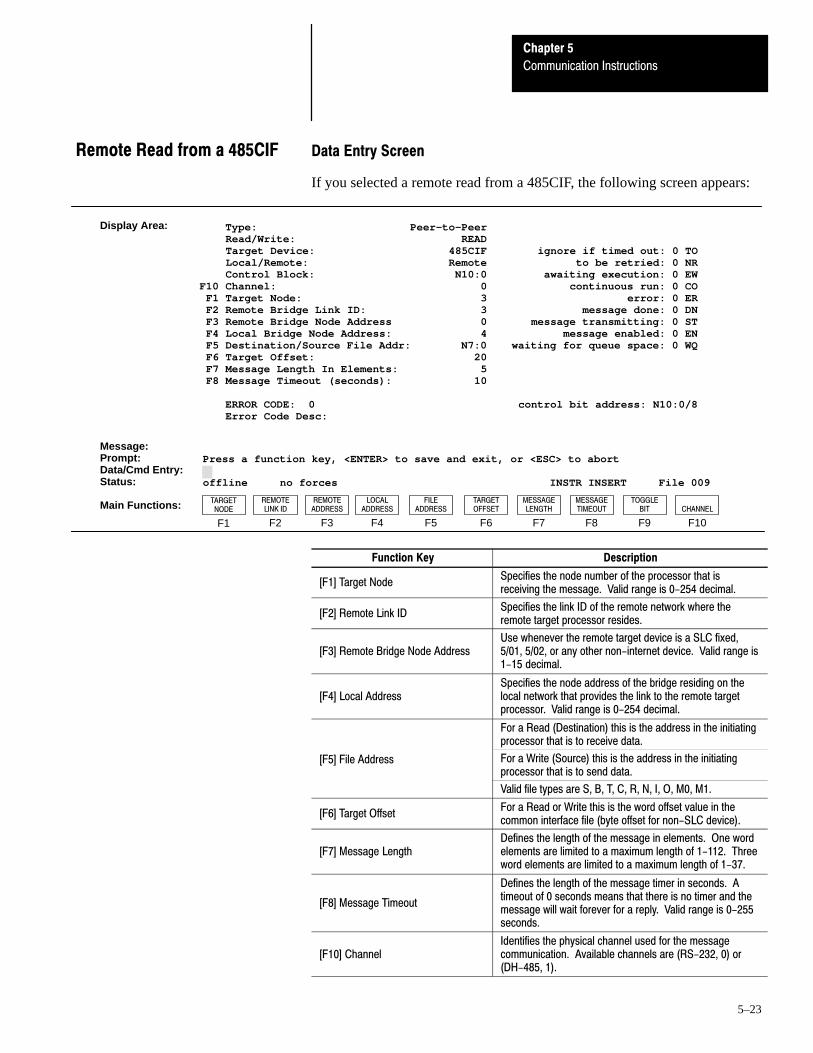
Chapter 5
Communication Instructions
5–23
Data Entry Screen
If you selected a remote read from a 485CIF, the following screen appears:
Type: Peer–to–Peer Read/Write: READ Target Device: 485CIF ignore if timed out: 0 TO Local/Remote: Remote to be retried: 0 NR Control Block: N10:0 awaiting execution: 0 EWF10 Channel: 0 continuous run: 0 CO F1 Target Node: 3 error: 0 ER F2 Remote Bridge Link ID: 3 message done: 0 DN F3 Remote Bridge Node Address 0 message transmitting: 0 ST F4 Local Bridge Node Address: 4 message enabled: 0 EN F5 Destination/Source File Addr: N7:0 waiting for queue space: 0 WQ F6 Target Offset: 20 F7 Message Length In Elements: 5 F8 Message Timeout (seconds): 10 ERROR CODE: 0 control bit address: N10:0/8 Error Code Desc:
Press a function key, <ENTER> to save and exit, or <ESC> to abort offline no forces INSTR INSERT File 009
Message:Prompt:Data/Cmd Entry:Status:
Main Functions:
F9
TOGGLEBIT
Display Area:
F1 F7F5 F6
TARGETNODE
MESSAGELENGTH
FILEADDRESS
TARGETOFFSET
F8
MESSAGETIMEOUT
F10CHANNEL
F2 F4
REMOTELINK ID
LOCALADDRESS
F3
REMOTEADDRESS
Function Key Description
[F1] Target NodeSpecifies the node number of the processor that isreceiving the message. Valid range is 0-254 decimal.
[F2] Remote Link IDSpecifies the link ID of the remote network where theremote target processor resides.
[F3] Remote Bridge Node AddressUse whenever the remote target device is a SLC fixed,5/01, 5/02, or any other non-internet device. Valid range is1-15 decimal.
[F4] Local AddressSpecifies the node address of the bridge residing on thelocal network that provides the link to the remote targetprocessor. Valid range is 0-254 decimal.
For a Read (Destination) this is the address in the initiatingprocessor that is to receive data.
[F5] File Address For a Write (Source) this is the address in the initiatingprocessor that is to send data.
Valid file types are S, B, T, C, R, N, I, O, M0, M1.
[F6] Target OffsetFor a Read or Write this is the word offset value in thecommon interface file (byte offset for non-SLC device).
[F7] Message LengthDefines the length of the message in elements. One wordelements are limited to a maximum length of 1-112. Threeword elements are limited to a maximum length of 1-37.
[F8] Message Timeout
Defines the length of the message timer in seconds. Atimeout of 0 seconds means that there is no timer and themessage will wait forever for a reply. Valid range is 0-255seconds.
[F10] ChannelIdentifies the physical channel used for the messagecommunication. Available channels are (RS-232, 0) or(DH-485, 1).
Remote Read from a 485CIF

Chapter 5
Communication Instructions
5–24
Monitor Display
The following screen allows you to monitor the status of the messageinstruction while the processor is running:
Type: Peer–to–Peer Read/Write: READ Target Device: 485CIF ignore if timed out: 0 TO Local/Remote: Remote to be retried: 0 NR Control Block: N10:0 awaiting execution: 0 EW Channel: 1 continuous run: 0 CO F1 Target Node: 3 error: 0 ER Remote Bridge Link ID: 3 message done: 0 DN Remote Bridge Node Address 0 message transmitting: 0 ST Local Bridge Node Address: 4 message enabled: 0 EN Destination/Source File Addr: N7:0 waiting for queue space: 0 WQ F6 Target Offset: 20 Message Length In Elements: 5 F8 Message Timeout (seconds): 10 ERROR CODE: 0 control bit address: N10:0/8 Error Code Desc:
Press a function key or press <ESC> to exit monitor offline no forces INSTR INSERT File 009
Message:Prompt:Data/Cmd Entry:Status:
Main Functions:
F9
TOGGLEBIT
Display Area:
F1 F6NODE
TARGETOFFSET
F8
MESSAGETIMEOUT
In the display above the 5/03 processor will read five elements (words) fromTarget node 3 of Remote Bridge Link ID 3, starting at byte offset 20 of itsPLC compatibility file. This is a byte offset because the device at node 3 is aPLC 5/40. The five elements will be placed in your integer file starting atword N7:0. If 10 seconds elapse without a reply, error bit N10:0/12 will beset, indicating that the instruction timed out. The device at node 3 of RemoteBridge Link ID 2 understands the 485CIF (PLC 2 emulation) protocol.
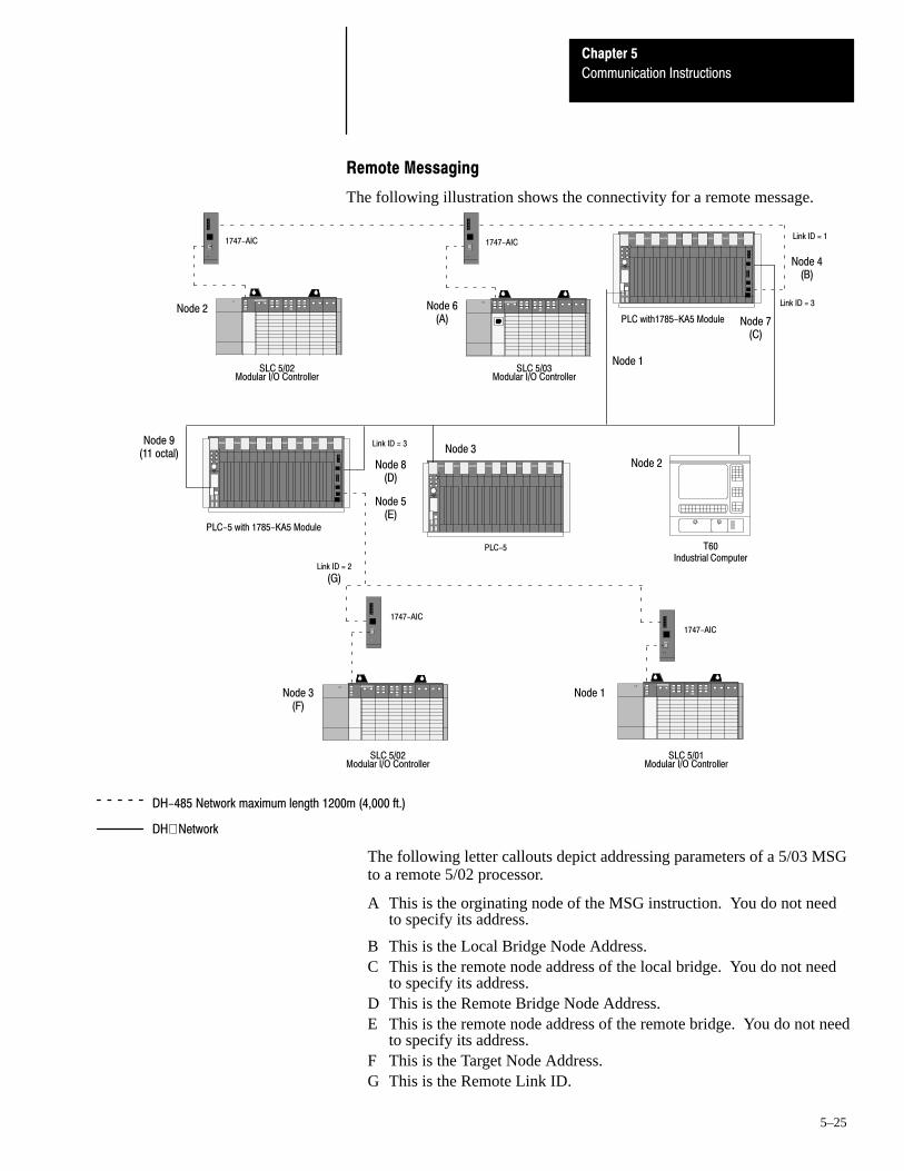
Chapter 5
Communication Instructions
5–25
Remote Messaging
The following illustration shows the connectivity for a remote message.
SLC 5/02Modular I/O Controller
1747-AIC
PLC-5
SLC 5/01Modular I/O Controller
SLC 5/03Modular I/O Controller
T60Industrial Computer
1747-AIC
1747-AIC
1747-AIC
SLC 5/02Modular I/O Controller
Link ID = 1
Link ID = 3
Link ID = 2
(G)
Node 2 Node 6(A)
Node 4(B)
Node 7(C)
PLC-5 with 1785-KA5 Module
Node 3Node 2
Link ID = 3
PLC with1785-KA5 Module
Node 8(D)
Node 5(E)
Node 3(F)
Node 1
DH-485 Network maximum length 1200m (4,000 ft.)
DH+ Network
Node 1
Node 9(11 octal)
The following letter callouts depict addressing parameters of a 5/03 MSGto a remote 5/02 processor.
A This is the orginating node of the MSG instruction. You do not needto specify its address.
B This is the Local Bridge Node Address.C This is the remote node address of the local bridge. You do not need
to specify its address.D This is the Remote Bridge Node Address.E This is the remote node address of the remote bridge. You do not need
to specify its address.F This is the Target Node Address.G This is the Remote Link ID.

Chapter 5
Communication Instructions
5–26
The following section describes the timing diagram for a 5/03 MSGinstruction.
Rung goes True Target nodereceives packet
Target node processes packetsuccessfully and returns data(read) or writes data (success)
EN
EW
ST
10
10
10
DN
ER
1010
WQ10
NR10
TO10
➄➀ ➁ ➂
1. When the MSG rung becomes true and the MSG is scanned, if there isroom in any of the four active MSG buffers, the EN and EW bits are set.Note that if this were a MSG Write instruction, the source data would betransferred to the MSG buffer at this time. If there is no room in the fourMSG buffers, but a position is available in the ten position MSG Queue,only the EN bit is set. The 10 position MSG Queue works on afirst–in–first–out basis that allows the 5/03 processor to remember theorder the MSG instructions were enabled. Note that the program does nothave access to the 5/03 MSG Queue.
If there is no room in any of the four MSG buffers and no room in the 10position MSG Queue, only the WQ bit is set. Note that when the WQ bitis set, the MSG instruction must be re–scanned at a later time when thereis room in either the four MSG buffers or the ten position MSG Queue.
Once the EN bit is set, it remains set until the entire MSG process iscomplete and either the DN, ER, or TO bit is set. The MSG Timeoutvalue begins timing when the EN bit is set. If the timeout period expiresbefore the MSG instruction completes it function, the ER bit is set and acode is placed in the MSG block to inform you of the timeout error.
If you choose to set the CO bit, your MSG instruction will “take up”permanent residence in one of the four active MSG buffers. The MSGinstruction will continue to re–transmit its data each time the DN or ERbit is set. If this were a MSG Write instruction, your source data wouldbe updated each MSG cycle.
Timing Diagram for aSuccessful 5/03 MSGInstruction
Chapter 5
Communication Instructions
5–27
2. At the next end of scan or SVC, the 5/03 processor determines if it shouldexamine the MSG Queue for “something to do.” The processor bases itsdecision on the state of bits S:2/15, S:33/7, S:33/5, S:33/6, networkcommunication requests from other nodes, and if previous MSGinstructions are already in progress. If the 5/03 processor determines thatit should not access the queue, the MSG instruction remains as it was.(Either the EN and EW bits remain set, or only the EN bit is set, or onlythe WQ bit is set until the next end of scan or SVC. If only the WQ bit isset, the MSG instruction must be re–scanned.)
If the 5/03 processor determines that it has “something to do,” it willunload the MSG Queue entries into the MSG buffers until all four MSGbuffers are full. Each MSG buffer will contain a valid network packet. Ifa packet cannot be successfully built from the MSG Queue, the ER bit isset and a code is placed in the MSG block to inform you of an error.When a MSG instruction is loaded into a MSG buffer, the EN and EWbits are set.
The 5/03 processor then exits the end of scan or SVC portion of the scan.The processor’s background communication function sends the packets tothe Target Nodes that you specified in your MSG instruction. Dependingon the state of bits S:2/15, S:33/7, S:33/5, and S:33/6 you can have up tofour MSG instructions active at any given time.
3. If the Target Node successfully receives the packet, it sends back an ACK(an acknowledge). The ACK causes the processor to clear the EW bitand set the ST bit. The Target Node has not yet examined the packet, tosee if it understands your request. Note that the Target Node is notrequired to respond within any give time frame.
Important: If the Target Node faults or power cycles during this timeframe of a MSG transaction, you will never receive a reply.This why it is recommended to use a MSG Timeout value inyour MSG instruction.
Step 4 not shown in the timing diagram.
4. If you do not receive an ACK, step 3 does not occur. Instead a NAK (noacknowledge) is received. When this happens, the ST bit remains clear.A NAK indicates:
• either the Target Node is not there,• it does not respond,• it is too busy, or• it receives a corrupt packet.
When a NAK occurs, the EW bit is cleared and the NR bit is set for onescan. The next time the MSG instruction is scanned, the ER bit is set andthe NR bit is cleared. This indicates that the MSG instruction failed.Note that if the Target Node is too busy, the ER bit is not set. Instead, theMSG instruction re–queues itself for re–transmission.
Chapter 5
Communication Instructions
5–28
5. Following the successful receipt of the packet, the Target Node sends areply packet. The reply packet will contain one of the followingresponses:
• I have successfully performed your write request.• I have successfully performed your read request, and here is your data.• I have not performed your request, you are in error.
At the next end of scan or SVC, following the Target Node’s reply, the5/03 processor examines the packet from the target device. If the replycontains “I have successfully performed your write request,” the DN bit isset and the ST bit is cleared. The MSG instruction function is complete.If the MSG rung is false, the EN bit is cleared the next time the MSGinstruction is scanned.
If the reply contains “I have successfully performed your read request,and here is your data,” the data is written to the data table, the DN bit isset and the ST bit is cleared. The MSG instruction function is complete.If the MSG rung is false, the EN bit is cleared the next time the MSGinstruction is scanned.
If the reply contains “I have not performed your request, you are in error,”the ER bit is set and the ST bit is cleared. The MSG instruction functionis complete. If the MSG rung is false, the EN bit is cleared the next timethe MSG instruction is scanned.
The four MSG buffers are shared between channel 0 and channel 1. Eachchannel has its own ten position MSG Queue. The 5/03 processor unloadsthe two MSG queues into the MSG buffers evenly at end of scan or SVC.This allows both channels equal access to communications. If you program aSVC instruction that is configured to service only one channel, then only thatchannel will have its MSG Queue unloaded into the MSG buffers (until thenext end of scan or SVC when both channels will again be unloaded evenly).

Chapter 5
Communication Instructions
5–29
Control Block Layouts for a 5/03 Processor
The control block layout if you select 500CPU as the target device:
EN ST DN ER CO EW NR TO Error Code
15 14 13 12 11 10 09 08 07 06 05 04 03 02 01 00
Node Number
Reserved for length in words
Word
0
1
2
File Number
File Type (S, B, T, C, R, N, O, I, M0, M1)
Element Number
Subelement Number
3
4
5
6
Reserved (Internal Messaging Bits)
Message Timer Preset
WQ
Reserved (Internal use only)
Message Timer Accumulator
7
8
9
10
11Reserved (Internal use only)
Read or Write, Local or Remote to a 500CPU
Reserved (Internal use only) 12
Reserved (Internal use only) 13
The control block layout if you select 485 CIF as the target device:
EN ST DN ER CO EW NR TO Error Code
15 14 13 12 11 10 09 08 07 06 05 04 03 02 01 00
Node Number
Reserved for length in words
Word
0
1
2
Offset in Words
Not Used
Not Used
Not Used
3
4
5
6
Reserved (Internal Messaging Bits)
Message Timer Preset
WQ
Reserved (Internal use only)
Message Timer Accumulator
7
8
9
10
11Reserved (Internal use only)
Read or Write, Local or Remote to a 485CIF
Reserved (Internal use only) 12
13Reserved (Internal use only)
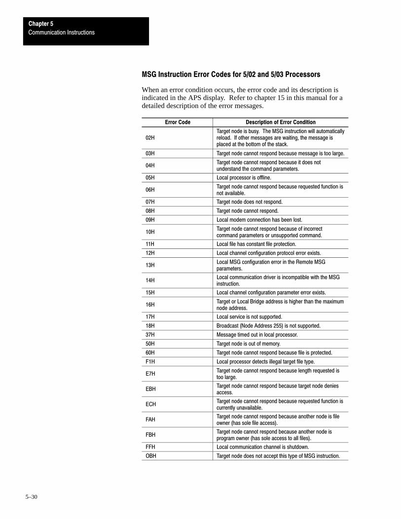
Chapter 5
Communication Instructions
5–30
MSG Instruction Error Codes for 5/02 and 5/03 Processors
When an error condition occurs, the error code and its description isindicated in the APS display. Refer to chapter 15 in this manual for adetailed description of the error messages.
Error Code Description of Error Condition
02HTarget node is busy. The MSG instruction will automaticallyreload. If other messages are waiting, the message isplaced at the bottom of the stack.
03H Target node cannot respond because message is too large.
04HTarget node cannot respond because it does notunderstand the command parameters.
05H Local processor is offline.
06HTarget node cannot respond because requested function isnot available.
07H Target node does not respond.
08H Target node cannot respond.
09H Local modem connection has been lost.
10HTarget node cannot respond because of incorrectcommand parameters or unsupported command.
11H Local file has constant file protection.
12H Local channel configuration protocol error exists.
13HLocal MSG configuration error in the Remote MSGparameters.
14HLocal communication driver is incompatible with the MSGinstruction.
15H Local channel configuration parameter error exists.
16HTarget or Local Bridge address is higher than the maximumnode address.
17H Local service is not supported.
18H Broadcast (Node Address 255) is not supported.
37H Message timed out in local processor.
50H Target node is out of memory.
60H Target node cannot respond because file is protected.
F1H Local processor detects illegal target file type.
E7HTarget node cannot respond because length requested istoo large.
EBHTarget node cannot respond because target node deniesaccess.
ECHTarget node cannot respond because requested function iscurrently unavailable.
FAHTarget node cannot respond because another node is fileowner (has sole file access).
FBHTarget node cannot respond because another node isprogram owner (has sole access to all files).
FFH Local communication channel is shutdown.
OBH Target node does not accept this type of MSG instruction.
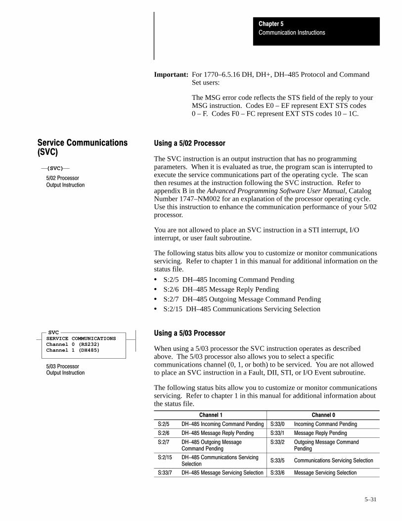
Chapter 5
Communication Instructions
5–31
Important: For 1770–6.5.16 DH, DH+, DH–485 Protocol and CommandSet users:
The MSG error code reflects the STS field of the reply to yourMSG instruction. Codes E0 – EF represent EXT STS codes0 – F. Codes F0 – FC represent EXT STS codes 10 – 1C.
Using a 5/02 Processor
The SVC instruction is an output instruction that has no programmingparameters. When it is evaluated as true, the program scan is interrupted toexecute the service communications part of the operating cycle. The scanthen resumes at the instruction following the SVC instruction. Refer toappendix B in the Advanced Programming Software User Manual, CatalogNumber 1747–NM002 for an explanation of the processor operating cycle.Use this instruction to enhance the communication performance of your 5/02processor.
You are not allowed to place an SVC instruction in a STI interrupt, I/Ointerrupt, or user fault subroutine.
The following status bits allow you to customize or monitor communicationsservicing. Refer to chapter 1 in this manual for additional information on thestatus file.
• S:2/5 DH–485 Incoming Command Pending• S:2/6 DH–485 Message Reply Pending• S:2/7 DH–485 Outgoing Message Command Pending• S:2/15 DH–485 Communications Servicing Selection
Using a 5/03 Processor
When using a 5/03 processor the SVC instruction operates as describedabove. The 5/03 processor also allows you to select a specificcommunications channel (0, 1, or both) to be serviced. You are not allowedto place an SVC instruction in a Fault, DII, STI, or I/O Event subroutine.
The following status bits allow you to customize or monitor communicationsservicing. Refer to chapter 1 in this manual for additional information aboutthe status file.
Channel 1 Channel 0
S:2/5 DH-485 Incoming Command Pending S:33/0 Incoming Command Pending
S:2/6 DH-485 Message Reply Pending S:33/1 Message Reply Pending
S:2/7 DH-485 Outgoing Message Command Pending
S:33/2 Outgoing Message Command Pending
S:2/15 DH-485 Communications Servicing Selection
S:33/5 Communications Servicing Selection
S:33/7 DH-485 Message Servicing Selection S:33/6 Message Servicing Selection
(SVC)
5/02 ProcessorOutput Instruction
Service Communications(SVC)
SVCSERVICE COMMUNICATIONSChannel 0 (RS232)Channel 1 (DH485)
Output Instruction5/03 Processor

Chapter 5
Communication Instructions
5–32
Channel Servicing
When a channel is not selected to be serviced by the SVC instruction, thatchannel is serviced normally at the end of the scan.
Application Example
The SVC instruction is used when you want to execute a communicationfunction, such as transmitting a message, prior to the normal servicecommunication portion of the operating scan. The following example showshow to selectively use the SVC instruction.
] [S:2
7(SVC)
Outgoing MessageCommand Pending Bit
You can place this rung after a message write instruction. S:2/7 is set whenthe message instruction is enabled and waiting (provided no message iscurrently being transmitted). When S:2/7 is set, the SVC instruction isevaluated as true and the program scan is interrupted to execute the servicecommunications portion of the operating scan. The scan then resumes at theinstruction following the SVC instruction.
This simple example assumes that the Comms Servicing Selection bit S:2/15is clear and that this is the only active MSG instruction.
Important: You may program the SVC instruction unconditionally acrossthe rails. This is the normal programming technique for theSVC instruction.
The 5/03 processor can pass a MSG instruction through one remote networkto its target destination. (You can make one hop across a network.) Or, the5/03 processor can pass a MSG instruction to the network that exists on theother side of the local bridge. Refer to the remote messaging diagram on5–25.
In the SLC 500 Read example (page 5–20), a MSG read instruction isinitiated from a 5/03 processor to a 5/02 target node that is located on aremote DH–485 network. In the 485CIF Read example (page 5–23), a MSGread instruction is initiated from a 5/03 processor to a 5/40 target node that islocated on the DH+ network that is located on the other side of the localbridge.
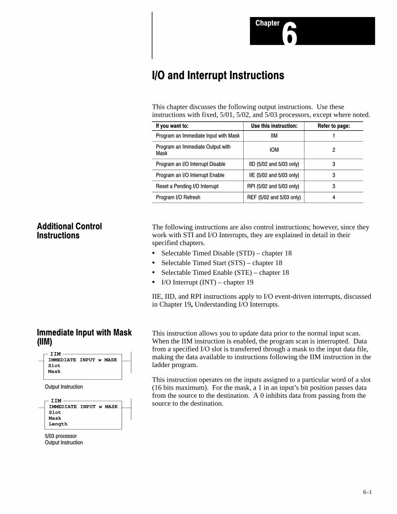
A–B 6Chapter
6–1
I/O and Interrupt Instructions
This chapter discusses the following output instructions. Use theseinstructions with fixed, 5/01, 5/02, and 5/03 processors, except where noted.
If you want to: Use this instruction: Refer to page:
Program an Immediate Input with Mask IIM 1
Program an Immediate Output withMask
IOM 2
Program an I/O Interrupt Disable IID (5/02 and 5/03 only) 3
Program an I/O Interrupt Enable IIE (5/02 and 5/03 only) 3
Reset a Pending I/O Interrupt RPI (5/02 and 5/03 only) 3
Program I/O Refresh REF (5/02 and 5/03 only) 4
The following instructions are also control instructions; however, since theywork with STI and I/O Interrupts, they are explained in detail in theirspecified chapters.
• Selectable Timed Disable (STD) – chapter 18• Selectable Timed Start (STS) – chapter 18• Selectable Timed Enable (STE) – chapter 18• I/O Interrupt (INT) – chapter 19
IIE, IID, and RPI instructions apply to I/O event-driven interrupts, discussedin Chapter 19, Understanding I/O Interrupts.
This instruction allows you to update data prior to the normal input scan.When the IIM instruction is enabled, the program scan is interrupted. Datafrom a specified I/O slot is transferred through a mask to the input data file,making the data available to instructions following the IIM instruction in theladder program.
This instruction operates on the inputs assigned to a particular word of a slot(16 bits maximum). For the mask, a 1 in an input’s bit position passes datafrom the source to the destination. A 0 inhibits data from passing from thesource to the destination.
Additional ControlInstructions
IIMIMMEDIATE INPUT w MASKSlotMask
Output Instruction
IIMIMMEDIATE INPUT w MASKSlotMaskLength
5/03 processorOutput Instruction
Immediate Input with Mask(IIM)

Chapter 6
I/O and Interrupt Instructions
6–2
Entering Parameters
Slot – Specify the input slot number and the word number pertaining to theslot. Word 0 of a slot need not be specified. Fixed and 5/01 processors canhave up to 8 words associated with the slot. The 5/02 and 5/03 processor canhave up to 32 words associated with the slot (0–31).
Example
I:2 Inputs of slot 2, word 0
I:2.1 Inputs of slot 2, word 1
I:1 Inputs of slot 1, word 0
Mask – Specify a Hex constant or register address.
Length – 5/03 specific, used to transfer more than one word per slot.
This instruction allows you to update the outputs prior to the normal outputscan. When the IOM instruction is enabled, the program scan is interruptedto transfer data to a specified I/O slot through a mask. The program scanthen resumes.
This instruction operates on the physical outputs assigned to a particularword of a slot (16 bits maximum). For the mask, a 1 in the output bitposition passes data from the source to the destination. A 0 inhibits the datafrom passing from the source to the destination.
Entering Parameters
Slot – Specify the slot number and the word number pertaining to the slot.Word 0 of a slot need not be specified. Fixed and 5/01 processors can haveup to 8 words associated with the slot. The 5/02 and 5/03 processor can haveup to 32 words associated with the slot (0–31).
Example
O:2 Outputs of slot 2, word 0
O:1 Outputs of slot 1, word 0
O:2.1 Outputs of slot 2, word 1
Mask – Specify a Hex constant or register address.
Length – 5/03 specific, used to transfer more than one word per slot.
IOMIMMEDIATE OUTPUT w MASKSlotMask
Output Instruction
IOMIMMEDIATE OUTPUT w MASKSlotMaskLength
5/03 processorOutput Instruction
Immediate Output with Mask(IOM)

Chapter 6
I/O and Interrupt Instructions
6–3
The I/O Event-Driven Interrupt function is used with specialty I/O modulescapable of generating an interrupt. You must specify a subroutine to beexecuted upon receipt of such an interrupt. Use these instructions with 5/02and 5/03 processors.
Important: Refer to chapter 19 before you use these instructions in yourprogram.
I/O Interrupt Disable and Enable (IID, IIE)
These instructions are generally used in pairs to prevent I/O interrupts fromoccurring during time-critical or sequence-critical portions of your mainprogram or subroutine.
Reset Pending I/O Interrupt (RPI)
This instruction resets the pending status of the specified slots and informsthe corresponding I/O modules that you have aborted their interrupt requests.
Entering Parameters
Enter the I/O slot numbers (1 to 30) involved. Examples:
6 indicates slot 6
6,8 indicates slots 6 and 8
6–8 indicates slots 6, 7, and 8
1–30 indicates all slots
I/O Event-Driven Interrupts
IIDI/O INTERRUPT DISABLESlots:
IIEI/O INTERRUPT ENABLESlots:
Output Instructions
RPIRESET PENDING INTERRUPTSlots:
Output Instruction
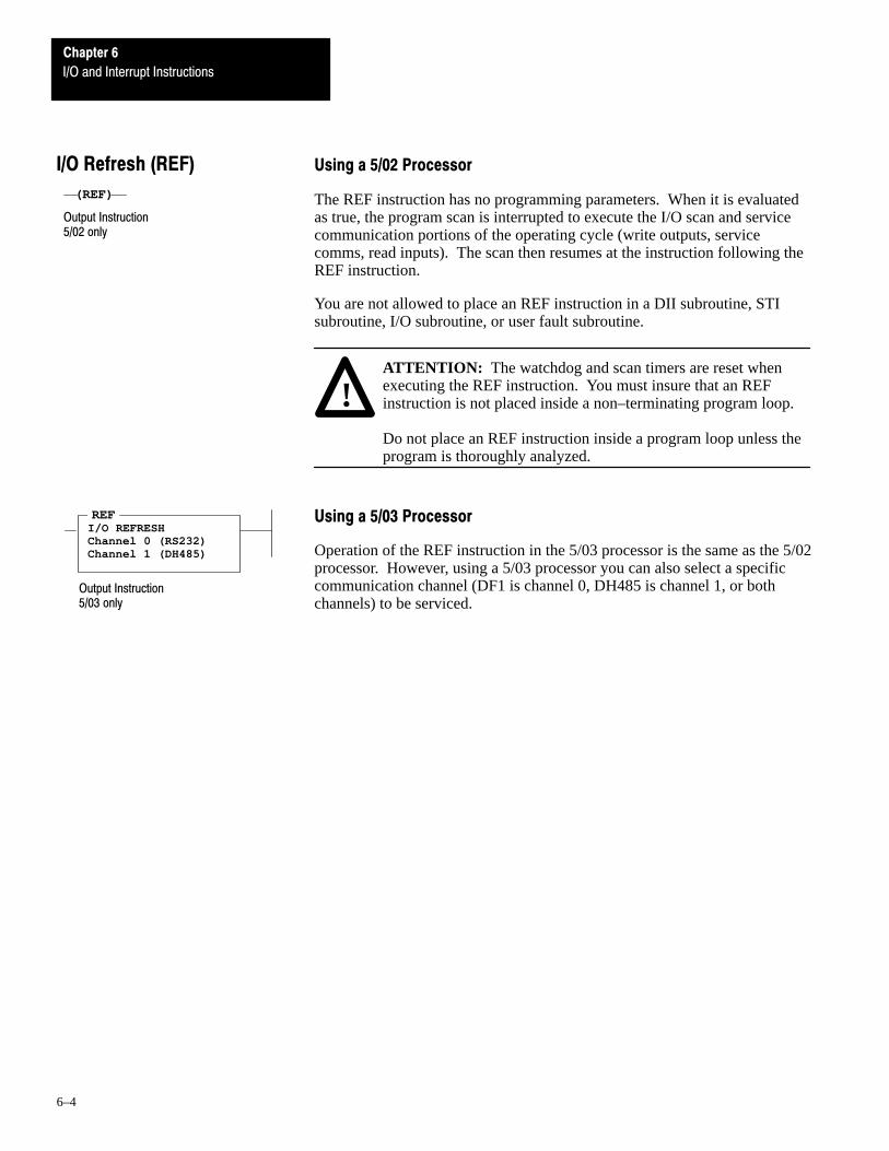
Chapter 6
I/O and Interrupt Instructions
6–4
Using a 5/02 Processor
The REF instruction has no programming parameters. When it is evaluatedas true, the program scan is interrupted to execute the I/O scan and servicecommunication portions of the operating cycle (write outputs, servicecomms, read inputs). The scan then resumes at the instruction following theREF instruction.
You are not allowed to place an REF instruction in a DII subroutine, STIsubroutine, I/O subroutine, or user fault subroutine.
!ATTENTION: The watchdog and scan timers are reset whenexecuting the REF instruction. You must insure that an REFinstruction is not placed inside a non–terminating program loop.
Do not place an REF instruction inside a program loop unless theprogram is thoroughly analyzed.
Using a 5/03 Processor
Operation of the REF instruction in the 5/03 processor is the same as the 5/02processor. However, using a 5/03 processor you can also select a specificcommunication channel (DF1 is channel 0, DH485 is channel 1, or bothchannels) to be serviced.
(REF)
Output Instruction5/02 only
I/O Refresh (REF)
REFI/O REFRESHChannel 0 (RS232)Channel 1 (DH485)
Output Instruction5/03 only

A–B 7Chapter
7–1
Comparison Instructions
The following input instructions allow you to compare values of data. Usethese instructions with fixed, 5/01, 5/02, and 5/03 processors, except wherenoted.
If you want to: Use this instruction: Refer to page:
Test whether two values areequal
EQU 1
Test whether one value is notequal to a second value
NEQ 2
Test whether one value is lessthan a second value
LES 2
Test whether one value is lessthan or equal to a second value
LEQ 2
Test whether one value isgreater than another
GRT 2
Test whether one value isgreater than or equal to asecond value
GEQ 3
Test portions of two values tosee whether they are equal
MEQ 3
Test whether one value is withinthe limit range of two othervalues
LIM (5/02 and 5/03 only) 3
The following general information applies to comparison instructions.
Indexed Word Addresses
With 5/02 and 5/03 processors, you have the option of using indexed wordaddresses for instruction parameters specifying word addresses. Indexedaddressing is discussed chapter 5 of the Advanced Programming SoftwareUser Manual, Catalog Number 1747–NM002.
Use the EQU instruction to test whether two values are equal. If source Aand source B are equal, the instruction is logically true. If these values arenot equal, the instruction is logically false.
Entering Parameters
You must enter a word address for source A. You can enter a programconstant or a word address for source B. Signed integers are stored in two’scomplementary form.
Comparison InstructionsOverview
EQUEQUALSource A
Source B
Input Instruction
Equal (EQU)

GRT, GEQ, MEQ, LIM
Chapter 7
Comparison Instructions EQU, NEQ, LES, LEQ
7–2
Use the NEQ instruction to test whether two values are not equal. If sourceA and source B are not equal, the instruction is logically true. If the twovalues are equal, the instruction is logically false.
Entering Parameters
You must enter a word address for source A. You can enter a programconstant or a word address for source B. Signed integers are stored in two’scomplementary form.
Use the LES instruction to test whether one value (source A) is less thananother (source B). If source A is less than the value at source B theinstruction is logically true. If the value at source A is greater than or equalto the value at source B, the instruction is logically false.
Entering Parameters
You must enter a word address for source A. You can enter a programconstant or a word address for source B. Signed integers are stored in two’scomplementary form.
Use the LEQ instruction to test whether one value (source A) is less than orequal to another (source B). If the value at source A is less than or equal tothe value at source B, the instruction is logically true. If the value at sourceA is greater than the value at source B, the instruction is logically false.
Entering Parameters
You must enter a word address for source A. You can enter a programconstant or a word address for source B. Signed integers are stored in two’scomplementary form.
Use the GRT instruction to test whether one value (source A) is greater thananother (source B). If the value at source A is greater than the value atsource B, the instruction is logically true. If the value at source A is less thanor equal to the value at source B, the instruction is logically false.
Entering Parameters
You must enter a word address for source A. You can enter a programconstant or a word address for source B. Signed integers are stored in two’scomplementary form.
NEQNOT EQUALSource A
Source B
Input Instruction
Not Equal (NEQ)
LESLESS THANSource A
Source B
Input Instruction
Less Than (LES)
LEQLESS THAN OR EQUALSource A
Source B
Input Instruction
Less Than or Equal (LEQ)
GRTGREATER THANSource A
Source B
Input Instruction
Greater Than (GRT)

GRT, GEQ, MEQ, LIM
Chapter 7
Comparison Instructions EQU, NEQ, LES, LEQ,
7–3
Use the GEQ instruction to test whether one value (source A) is greater thanor equal to another (source B). If the value at source A is greater than orequal to the value at source B, the instruction is logically true. If the value atsource A is less than the value at source B, the instruction is logically false.
Entering Parameters
You must enter a word address for source A. You can enter a programconstant or a word address for source B. Signed integers are stored in two’scomplementary form.
Use the MEQ instruction to compare data at a source address with data at areference address. Use of this instruction allows portions of the data to bemasked by a separate word.
Entering Parameters
• Source is the address of the value you want to compare.• Mask is the address of the mask through which the instruction moves
data. The mask can be a hexadecimal value.• Compare is an integer value or the address of the reference.
If the 16 bits of data at the source address are equal to the 16 bits of data atthe compare address (less masked bits), the instruction is true. Theinstruction becomes false as soon as it detects a mismatch. Bits in the maskword mask data when reset; they pass data when set.
Use the LIM instruction to test for values within or outside a specified range,depending on how you set the limits. Use this instruction with 5/02 and 5/03processors.
Entering Parameters
To program the LIM instruction you must provide the Low Limit, Test, andHigh Limit values. These values can be word addresses or programconstants, restricted to the following combinations:
• If the Test parameter is a program constant, both the Low Limit and HighLimit parameters must be word addresses.
• If the Test parameter is a word address, the Low Limit and High Limitparameters can be either a program constant or a word address.
GEQGRTR THAN OR EQUALSource A
Source B
Input Instruction
Greater Than or Equal (GEQ)
MEQMASKED EQUALSource
Mask
Compare
Input Instruction
Masked Comparison for Equal(MEQ)
LIMLIMIT TESTLow Lim
Test
High Lim
Input Instruction
Limit Test (LIM)

GRT, GEQ, MEQ, LIM
Chapter 7
Comparison Instructions EQU, NEQ, LES, LEQ
7–4
True/False Status of the Instruction
If the Low Limit has a value equal to or less than the High Limit, theinstruction is true when the Test value is between the limits or is equal toeither limit. If the Test value is outside the limits, the instruction is false.This is illustrated in the figure below.
Example, low limit less than high limit:
LowLimit
HighLimit
Instruction is Truewhen Test value is
Instruction is Falsewhen Test value is
5 8 5 thru 8 -32,768 thru 4 and 9 thru 32,767
False True False
–32,768Low Limit High Limit
+ 32,767
If the Low Limit has a value greater than the High Limit, the instruction isfalse when the Test value is between the limits. If the Test value is equal toeither limit or outside the limits, the instruction is true. This is illustrated inthe figure below.
8 5 -32,768 thru 5 and 8 thru 32,767 6 and 7
Example, low limit greater than high limit:
LowLimit
HighLimit
Instruction is Truewhen Test value is
Instruction is Falsewhen Test value is
True False True
–32,768High Limit Low Limit
+ 32,767
A–B 8Chapter
8–1
Math Instructions
The following output instructions allow you to perform computation andmath operations on individual words. Use these instructions with fixed, 5/01,5/02, and 5/03 processors, except where noted.
If you want to: Use this instruction: Refer to page:
Add two values ADD 3
Subtract two values SUB 3
Multiply one value from another MUL 6
Divide one value by another DIV 6
Perform a double divide DDV 7
Change the sign of the sourcevalue and place it in thedestination
NEG 7
Set all bits of a word to zero CLR 8
Convert an integer to BCD TOD 8
Convert a BCD value to aninteger value
FRD 11
Multiplex data DCD 14
Find the square root of a value SQR (5/02 and 5/03 only) 15
Scale a value SCL (5/02 and 5/03 only) 15
Application Techniques with 5/02 Series C and later and 5/03 processors
• 32-bit addition and subtractionRefer to chapter 1 in this manual for details concerning bit S:2/14.
The following general information applies to math instructions.
Instruction Parameters
• Source is the address(es) of the value(s) on which the mathematical,logical, or move operation is to be performed. This can be wordaddresses or program constants. An instruction that has two sourceoperands does not accept program constants in both operands.
• Destination is the address of the result of the operation. Signed integersare stored in two’s complementary form and apply to both source anddestination parameters.
Math Instructions Overview
NEG, CLR, TOD, FRD, DCD, SQR, SCL
Chapter 8
Math Instructions ADD, SUB, MUL, DIV, DDV,
8–2
Indexed Word Addresses
With 5/02 and 5/03 processors, you have the option of using indexed wordaddresses for instruction parameters specifying word addresses. Indexedaddressing is discussed in chapter 5 of the Advanced Programming SoftwareUser Manual, Catalog Number 1747–NM002.
Using Arithmetic Status Bits
After an instruction is executed, the arithmetic status bits in the status file areupdated:
• Carry (C), S:0/0 – Set if a carry is generated; otherwise cleared.• Overflow (V), S:0/1 – Indicates that the actual result of a math instruction
does not fit in the designated destination.• Zero (Z), S:0/2 – Indicates a 0 value after a math, move or logic
instruction.• Sign (S), S:0/3 – Indicates a negative (less than 0) value after a math,
move, or logic instruction.
Overflow Trap Bit, S:5/0
Minor error bit (S:5/0) is set upon detection of a mathematical overflow ordivision by zero. If this bit is set upon execution of an END statement, aTND instruction, or a REF instruction, the recoverable major error code 0020is declared.
Math Register, S:13 and S:14
Status word S:13 contains the least significant word of the 32-bit values ofthe MUL and DDV instructions. It contains the remainder for DIV and DDVinstructions. It also contains the first four BCD digits for the FRD and TODinstructions.
In applications where a math overflow or divide by zero occurs, you canavoid a CPU fault by using an unlatch (OTU) instruction with address S:5/0in your program. The rung must be between the overflow point and theEND, TND, or REF statement.
Status word S:14 contains the most significant word of the 32-bit values ofthe MUL and DDV instructions. It contains the unrounded quotient for DIVand DDV instructions. It also contains the most significant digit (digit 5) forTOD and FRD instructions.
NEG, CLR, TOD, FRD, DCD, SQR, SCL
Chapter 8
Math Instructions ADD, SUB, MUL, DIV, DDV,
8–3
Use the ADD instruction to add one value (source A) to another value(source B) and place the result in the destination.
Arithmetic Status Bits
With this Bit: The Processor:
Carry (C) sets if carry is generated; otherwise resets.
Overflow (V)
sets if overflow is detected at destination; otherwise resets.On overflow, the minor error flag is also set. The value-32,768 or 32,767 is placed in the destination. Exception:If you are using a Series C or later 5/02 or 5/03 processorand have S:2/14 (math overflow selection bit) set, then theunsigned, truncated overflow remains in the destination.
Zero (Z) sets if result is zero; otherwise resets.
Sign (S) sets if result is negative; otherwise resets.
Math Register
Contents unchanged.
Use the SUB instruction to subtract one value (Source B) from another(source A) and place the result in the destination.
Arithmetic Status Bits
With this Bit: The Processor:
Carry (C) sets if borrow is generated; otherwise resets.
Overflow (V)
sets if underflow; otherwise reset. On underflow, the minorerror flag is also set. The value -32,768 or 32,767 isplaced in the destination. Exception: If you are using aSeries C or later 5/02 or 5/03 processor and have S:2/14(math overflow selection bit) set, then the unsigned,truncated overflow remains in the destination.
Zero (Z) sets if result is zero; otherwise resets.
Sign (S) sets if result is negative; otherwise resets.
Math Register
Contents unchanged.
ADDADDSource A
Source B
Dest
Output Instruction
Add (ADD)
SUBSUBTRACTSource A
Source B
Dest
Output Instruction
Subtract (SUB)

NEG, CLR, TOD, FRD, DCD, SQR, SCL
Chapter 8
Math Instructions ADD, SUB, MUL, DIV, DDV,
8–4
With the Series C 5/02 processor and the 5/03 processor, you have the optionof performing 16-bit signed integer addition and subtraction (same asSeries B 5/02 processors) or 32-bit signed integer addition and subtraction.This is facilitated by status file bit S:2/14 (math overflow selection bit).
Math Overflow Selection Bit S:2/14
Set this bit when you intend to use 32-bit addition and subtraction. WhenS:2/14 is set, and the result of an ADD, SUB, MUL, DIV, or NEG instructioncannot be represented in the destination address (due to math underflow oroverflow):
• The overflow bit S:0/1 is set.• The overflow trap bit S:5/0 is set.• The destination address contains the unsigned truncated least significant
16 bits of the result.
The default condition of S:2/14 is reset (0). This provides the same operationas that of the Series B 5/02 processor. When S:2/14 is reset, and the result ofan ADD, SUB, MUL, DIV, or NEG instruction cannot be represented in thedestination address (underflow or overflow):
• The overflow bit S:0/1 is set.• The overflow trap bit S:5/0 is set.• The destination address contains 32767 if the result is positive or –32768
if the result is negative.
Note that the status of bit S:2/14 has no effect on the DDV instruction. Also,it has no effect on the math register content when using MUL and DIVinstructions.
Important: The 5/03 processor only interrogates this bit upon going to theRun mode. Any changes made to this bit while in the Runmode has no effect on system operation. Use the Data Monitorfunction to make this selection prior to entering the Run mode.
Example of 32-bit Addition
The following example shows how a 16-bit signed integer is added to a32-bit signed integer. Remember that S:2/14 must be set for 32-bit addition.
Note that the value of the most significant 16 bits (B3:3) of the 32-bitnumber is increased by 1 if the carry bit S:0/0 is set and it is decreased by 1 ifthe number being added (B3:1) is negative.
To avoid a major error from occurring at the end of the scan, you mustunlatch overflow trap bit S:5/0 as shown.
32�Bit Addition andSubtraction-Series C and Later5/02 and 5/03 Processors
NEG, CLR, TOD, FRD, DCD, SQR, SCL
Chapter 8
Math Instructions ADD, SUB, MUL, DIV, DDV,
8–5
(U) S:5
0END
] [B3
0[OSR]
B3
1
When rung goes true for asingle scan, B3:1 is addedto B3:2. The result isplaced in B3:2.
SUBSUBTRACTSource A B3:3
0000000000000011Source B 1
Dest B3:30000000000000011
ADDADDSource A B3:1
0101010110101000Source B B3:2
0001100101000000Dest B3:2
0001100101000000
ADDADDSource A 1
Source B B3:30000000000000011
Dest B3:30000000000000011
] [S:0
0
] [B3
31
Add 16-bit value B3:1 to 32-bit value B3:3 B3:2
Add Operation Binary Hex Decimal
B3:3 B3:2B3:1
B3:3 B3:2
0000 0000 0000 0011 0001 1001 0100 00000101 0101 1010 1000
0000 0000 0000 0011 0110 1110 1110 1000
0003 194055A8
0003 6EE8
203,07221,928
225,000
AddendAddend
Sum
➀
If a carry is generated (S:0/0set), 1 is added to B3:3.
If B3:1 is negative (B3/31set), 1 is subtracted fromB3:3.
Overflow trap bit S:5/0 isunlatched to prevent a majorerror from occurring at theend of the scan.
➀
The programming device displays 16-bit decimal values only. The decimal value of a 32-bit integer is derived fromthe displayed binary or hex value. For example, 0003 1940 Hex is 164x3 + 163x1 + 162x9 + 161x4 + 160x0 = 203,072.
Application Note: You can use the rung above with a DDV instruction anda counter to find the average value of B3:1.

NEG, CLR, TOD, FRD, DCD, SQR, SCL
Chapter 8
Math Instructions ADD, SUB, MUL, DIV, DDV,
8–6
Use the MUL instruction to multiply one value (source A) by another(source B) and place the result in the destination.
Arithmetic Status Bits
With this Bit: The Processor:
Carry (C) always resets.
Overflow (V)
sets if overflow is detected at destination; otherwise resets.On overflow, the minor error flag is also set. The value-32,768 or 32,767 is placed in the destination. Exception:If you are using a Series C or later 5/02 or 5/03 processorand have S:2/14 (math overflow selection bit) set, then theunsigned, truncated overflow remains in the destination.
Zero (Z) sets if result is zero; otherwise resets.
Sign (S) sets if result is negative; otherwise resets.
Math Register
Contains the 32–bit signed integer result of the multiply operation. Thisresult is valid at overflow.
Use the DIV instruction to divide one value (source A) by another(source B). The rounded quotient is then placed in the destination. If theremainder is 0.5 or greater, round up occurs in the destination. Theunrounded quotient is stored in the most significant word of the mathregister. The remainder is placed in the least significant word of the mathregister.
Arithmetic Status Bits
With this Bit: The Processor:
Carry (C) always resets.
Overflow (V)
sets if division by zero or overflow is detected; otherwiseresets. On overflow, the minor error flag is also set. Thevalue 32,767 is placed in the destination. Exception: If youare using a Series C or later 5/02 or 5/03 processor andhave S:2/14 (math overflow selection bit) set, then theunsigned, truncated overflow remains in the destination.
Zero (Z)sets if result is zero; otherwise resets; undefined if overflowis set.
Sign (S)sets if result is negative; otherwise resets; undefined ifoverflow is set.
Math Register
The unrounded quotient is placed in the most significant word, the remainderis placed in the least significant word.
MULMULTIPLYSource A
Source B
Dest
Output Instruction
Multiply (MUL)
DIVDIVIDESource A
Source B
Dest
Output Instruction
Divide (DIV)
NEG, CLR, TOD, FRD, DCD, SQR, SCL
Chapter 8
Math Instructions ADD, SUB, MUL, DIV, DDV,
8–7
The content of the math register is divided by the source value. The roundedquotient is placed in the destination. If the remainder is 0.5 or greater, roundup occurs in the destination. The unrounded quotient is placed in the mostsignificant word of the math register. The remainder is placed in the leastsignificant word of the math register.
Arithmetic Status Bits
With this Bit: The Processor:
Carry (C) always resets.
Overflow (V)
sets if division by zero or if result is greater than 32,767 orless than -32,768; otherwise resets. On overflow, theminor error flag is also set. The value 32,767 is placed inthe destination.
Zero (Z) sets if result is zero; otherwise resets.
Sign (S)sets if result is negative; otherwise resets; undefined ifoverflow is set.
Math Register
Initially contains the dividend of the DDV operation. Upon instructionexecution the unrounded quotient is placed in the most significant word ofthe math register. The remainder is placed in the least significant word of themath register.
Use the NEG instruction to change the sign of the source and then place it inthe destination. The destination contains the two’s complement of thesource. For example, if the source is 5, the destination would be –5.
Arithmetic Status Bits
With this Bit: The Processor:
Carry (C) clears if 0 or overflow, otherwise sets.
Overflow (V)
sets if overflow, otherwise reset. On overflow, the minorerror flag is also set. The value 32,767 is placed in thedestination. Exception: If you are using a Series C or later5/02 or 5/03 processor and have S:2/14 set, then theunsigned, truncated overflow remains in the destination.
Zero (Z) sets if result is zero; otherwise resets.
Sign (S) sets if result is negative; otherwise resets.
Math Register
Contents unchanged.
DDVDOUBLE DIVIDESource
Dest
Output Instruction
Double Divide (DDV)
NEGNEGATESource
Dest
Output Instruction
Negate (NEG)

NEG, CLR, TOD, FRD, DCD, SQR, SCL
Chapter 8
Math Instructions ADD, SUB, MUL, DIV, DDV,
8–8
Use the CLR instruction to set the destination value of a word to zero.
Arithmetic Status Bits
With this Bit: The Processor:
Carry (C) always resets.
Overflow (V) always resets.
Zero (Z) always sets.
Sign (S) always resets.
Math Register
Contents unchanged.
Use this instruction to convert 16–bit integers into BCD values.
With fixed and 5/01 processors, the destination can only be the math register.With 5/02 and 5/03 processors, the destination parameter can be a wordaddress in any data file, or it can be the math register, S:13 and S:14.
If the integer value you enter is negative, the sign is ignored and theconversion occurs as if the number were positive. For example, the absolutevalue of the number is used for conversion.
Arithmetic Status Bits
With this Bit: The Processor:
Carry (C) always resets.
Overflow (V)sets if the BCD result is larger than 9999. Overflow resultsin a minor error.
Zero (Z) sets if destination value is zero.
Sign (S) sets if the source word is negative; otherwise resets.
Math Register (when used)
Contains the 5–digit BCD result of the conversion. This result is valid atoverflow.
CLRCLEARDest
Output Instruction
Clear (CLR)
TODTO BCDSource
Dest
TODTO BCDSource
Dest S:1300000000
5/02 and 5/03 ProcessorsOutput Instruction
Fixed, 5/01 ProcessorsOutput Instruction
Convert to BCD (TOD)

NEG, CLR, TOD, FRD, DCD, SQR, SCL
Chapter 8
Math Instructions ADD, SUB, MUL, DIV, DDV,
8–9
Example 1 – 5/02 and 5/03 processors
The integer value 9760 stored at N7:3 is converted to BCD and the BCDequivalent is stored in N10:0. The maximum BCD value possible is 9999.
TODTO BCDSource N7:3
9760Dest N10:0
9760
APS displays the destination value inBCD (in the data monitor, N10:0 isdisplayed as -26784, decimal).
9 7 6 0
9 7 6 0
N7:3 Decimal 0010 0110 0010 0000
N10:0 4-digit BCD 1001 0111 0110 0000
Example 2 – Fixed, 5/01, 5/02, and 5/03 processors
The integer value 32760 stored at N7:3 is converted to BCD. The 5-digitBCD value is stored in the math register. The lower 4 digits of the BCDvalue is moved to output word O:2 and the remaining digit is moved througha mask to output word O:3.
When using the math register as the destination parameter in the TODinstruction, the maximum BCD value possible is 32767. However, for BCDvalues above 9999, the overflow bit is set, resulting in minor error bit S:5/0also being set. Your ladder program can unlatch S:5/0 before the end of thescan to avoid major error 0020, as done in this example.

NEG, CLR, TOD, FRD, DCD, SQR, SCL
Chapter 8
Math Instructions ADD, SUB, MUL, DIV, DDV,
8–10
TODTO BCDSource N7:3
32760Dest S:13
00032760
(U) S:5
0] [
S:0
1
APS displays S:13 andS:14 in BCD.
MOVMOVESource S:13
10080Dest O:2.0
10080
MVMMASKED MOVESource S:14
3Mask 000F
Dest O:3.03
] [
0 0 0 3 2 7 6 0
3 2 7 6 0
0 01515
N7:3 Decimal
S:13 & S:14 5-digit BCD
S:14 S:13
This example will output the absolute value (0-32767)contained in N7:3 as 5 BCD digits in output slots 2 and 3.
Minor Error Bit
0010 0111 0110 0000
0000 0000 0000 0011
Overflow Bit

NEG, CLR, TOD, FRD, DCD, SQR, SCL
Chapter 8
Math Instructions ADD, SUB, MUL, DIV, DDV,
8–11
Use this instruction to convert BCD values to integer values. With fixed and5/01 processors, the source can only be the math register. With 5/02 and5/03 processors, the source parameter can be a word address in any data file,or it can be the math register, S:13.
Arithmetic Status Bits
With this Bit: The Processor:
Carry (C) always resets.
Overflow (V)sets if non-BCD value is contained at the source or thevalue to be converted is greater than 32,767; otherwisereset. Overflow results in a minor error.
Zero (Z) sets if destination value is zero.
Sign (S) always resets.
Important: We recommend that you always provide ladder logic filtering ofall BCD input devices prior to performing the FRD instruction.The slightest difference in point–to–point input filter delay cancause the FRD instruction to overflow due to the conversion ofa non–BCD digit.
]/[S:1
15
EQUEQUALSource A N7:1
Source B I:2
MOVMOVESource I:2
Dest N7:1
FRDFROM BCDSource I:2
Dest N7:2
In the above example, the two rungs cause the processor to verify that thevalue at slot 2 (I:2) remains the same for two consecutive scans before it willexecute the FRD. This prevents the FRD from converting a non–BCD valueduring an input value change.
Math Register (when used)
Used as the source for converting the entire number range of a register.
FRDFROM BCDSource
Dest
FRDFROM BCDSource S:13
00000000Dest
5/02 and 5/03 ProcessorsOutput Instruction
Fixed and 5/01 ProcessorsOutput Instruction
Convert from BCD (FRD)

NEG, CLR, TOD, FRD, DCD, SQR, SCL
Chapter 8
Math Instructions ADD, SUB, MUL, DIV, DDV,
8–12
Example 1 – 5/02 and 5/03 processors
The BCD value 9760 at source N7:3 is converted and stored in N10:0. Themaximum source value is 9999, BCD.
APS displays source in BCD.
9 7 6 0
9 7 6 0 N7:3 4-digit BCD 1001 0111 0110 0000
N10:0 Decimal 0010 0110 0010 0000
FRDFROM BCDSource N7:3
9760Dest N10:0
9760
Example 2 – Fixed, 5/01, 5/02, and 5/03 Processors
The BCD value 32760 in the math register is converted and stored in N10:0.The maximum source value is 32767, BCD.
0 0 0 3 2 7 6 0
3 2 7 6 0
0 01515 5-digit BCDS:14 S:13
0000 0000 0000 0011 0010 0111 0110 0000
N10:0 Decimal 0111 1111 1111 1000
FRDFROM BCDSource S:13
00032760Dest N10:0
32760
APS displays S:13and S:14 in BCD.
You should convert BCD values to integer before you manipulate them inyour ladder program. If you do not convert the values, the processormanipulates them as integer and their value is lost.
Important: If the math register (S:13 and S:14) is used as the source for theFRD instruction and the BCD value does not exceed 4 digits, besure to clear word S:14 before executing the FRD instruction.If S:14 is not cleared and a value is contained in this word fromanother math instruction located elsewhere in the program, anincorrect decimal value will be placed in the destination word.

NEG, CLR, TOD, FRD, DCD, SQR, SCL
Chapter 8
Math Instructions ADD, SUB, MUL, DIV, DDV,
8–13
Clearing S:14 before executing the FRD instruction is shown below:
CLRCLEARDest S:14
0
FRDFROM BCDSource S:13
00001234Dest N7:0
1234
APS displays S:13 andS:14 in BCD.
MOVMOVESource N7:2
4660Dest S:13
4660
] [I:1
0 0001 0010 0011 0100
0000 0100 1101 0010
When the input condition is set (1), a BCD value (transferred from a 4–digitthumbwheel switch for example) is moved from word N7:2 into the mathregister. Status word S:14 is then cleared to make certain that unwanted datais not present when the FRD instruction is executed.

NEG, CLR, TOD, FRD, DCD, SQR, SCL
Chapter 8
Math Instructions ADD, SUB, MUL, DIV, DDV,
8–14
When the rung is true, this output instruction turns On one bit of thedestination word. The particular bit that is turned On depends on the valueof the first four bits of the source word. See the table below.
Use this instruction to multiplex data and for applications such as rotaryswitches, keypads, bank switching, etc.
Source Destination
Bit 15–04 03 02 01 00 15 14 13 12 11 10 09 08 07 06 05 04 03 02 01 00
x 0 0 0 0 0 0 0 0 0 0 0 0 0 0 0 0 0 0 0 1 x 0 0 0 1 0 0 0 0 0 0 0 0 0 0 0 0 0 0 1 0 x 0 0 1 0 0 0 0 0 0 0 0 0 0 0 0 0 0 1 0 0 x 0 0 1 1 0 0 0 0 0 0 0 0 0 0 0 0 1 0 0 0 x 0 1 0 0 0 0 0 0 0 0 0 0 0 0 0 1 0 0 0 0 x 0 1 0 1 0 0 0 0 0 0 0 0 0 0 1 0 0 0 0 0 x 0 1 1 0 0 0 0 0 0 0 0 0 0 1 0 0 0 0 0 0 x 0 1 1 1 0 0 0 0 0 0 0 0 1 0 0 0 0 0 0 0 x 1 0 0 0 0 0 0 0 0 0 0 1 0 0 0 0 0 0 0 0 x 1 0 0 1 0 0 0 0 0 0 1 0 0 0 0 0 0 0 0 0 x 1 0 1 0 0 0 0 0 0 1 0 0 0 0 0 0 0 0 0 0 x 1 0 1 1 0 0 0 0 1 0 0 0 0 0 0 0 0 0 0 0 x 1 1 0 0 0 0 0 1 0 0 0 0 0 0 0 0 0 0 0 0 x 1 1 0 1 0 0 1 0 0 0 0 0 0 0 0 0 0 0 0 0 x 1 1 1 0 0 1 0 0 0 0 0 0 0 0 0 0 0 0 0 0 x 1 1 1 1 1 0 0 0 0 0 0 0 0 0 0 0 0 0 0 0
Entering Parameters
• Source is the address that contains the bit decode information. Only thefirst four bits (0–3) are used by the DCD instruction. The remaining bitsmay be used for other application specific needs. Change the value of thefirst four bits of this word to select one bit of the destination word.
• Destination is the address of the word to be decoded. Only one bit of thisword is turned on at any one time, depending on the value of the sourceword.
Arithmetic Status Bits
Unaffected.
Math Register
Contents unchanged.
DCDDECODE 4 to 1 of 16Source
Dest
Output Instruction
Decode 4 to 1 of 16 (DCD)
NEG, CLR, TOD, FRD, DCD, SQR, SCL
Chapter 8
Math Instructions ADD, SUB, MUL, DIV, DDV,
8–15
When this instruction is evaluated as true, the square root of the absolutevalue of the source is calculated and the rounded result is placed in thedestination. Use this instruction with 5/02 and 5/03 processors.
The instruction calculates the square root of a negative number withoutoverflow or faults. In applications where the source value may be negative,use a comparison instruction to evaluate the source value to determine if thedestination may be invalid.
Arithmetic Status Bits
With this Bit: The Processor:
Carry (C) is reserved.
Overflow (V) always resets.
Zero (Z) sets when destination value is zero.
Sign (S) always resets.
Math Register
Contents unchanged.
When this instruction is true, the value at the source address is multiplied bythe rate value. The rounded result is added to the offset value and placed inthe destination. Use this instruction with 5/02 and 5/03 processors.
ExampleSCL
SCALESource N7:0
100Rate [/10000] 25000
Offset 127
Dest N7:1377
The source 100 is multiplied by25000 and divided by 10000 andadded to 127. The result 377 isplaced in the destination.
Important: Anytime an underflow or overflow occurs in the destinationfile, minor error bit S:5/0 must be reset by the program. Thismust occur before the end of the current scan to prevent majorerror code 0020 from being declared. This instruction canoverflow before the offset is added.
Note that the term rate is sometimes referred to as slope. The rate function islimited to the range −3.2768 to 3.2767. For example, −32768/10000 to+32767/10000.
SQRSQUARE ROOTSource
Dest
Output Instruction
Square Root (SQR)
SCLSCALESource
Rate [/10000]
Offset
Dest
Output Instruction
Scale Data (SCL)
NEG, CLR, TOD, FRD, DCD, SQR, SCL
Chapter 8
Math Instructions ADD, SUB, MUL, DIV, DDV,
8–16
Entering Parameters
The value for the following parameters is between –32,768 to 32,767.
• Source can be a program constant or a word address.• Rate (or slope) is the positive or negative value you enter divided by
10,000. It can be a program constant or a word address.• Offset can be a program constant or a word address.
Arithmetic Status Bits
With this Bit: The Processor:
Carry (C) is reserved.
Overflow (V)
sets if an overflow is detected; otherwise resets. Onoverflow, minor error bit S:5/0 is also set and the value-32,768 or 32,767 is placed in the destination. Thepresence of an overflow is checked before and after theoffset value is applied.➀
Zero (Z) sets when destination value is zero.
Sign (S) sets if the destination value is negative; otherwise resets.
➀ If the result of the Source times the Rate, divided by 10000 is greater than 32767, the SCL instructionoverflows, causing error 0020 (Minor Error Bit), and places 32767 in the Destination. This occurs regardless ofthe current offset.
Math Register
Contents unchanged.
NEG, CLR, TOD, FRD, DCD, SQR, SCL
Chapter 8
Math Instructions ADD, SUB, MUL, DIV, DDV,
8–17
Application Example 1 – Converting 4mA–20mA Analog Input Signal toPID Process Variable
Scaled Value
Input Value
3,277(Input Min.)
16,384(Input Max.)
16,383
0
(Scaled Max.)
(Scaled Min.)
Calculating the Linear Relationship
Use the following equations to express the linear relationship between theinput value and the resulting scaled value:
Scaled value = (input value x rate) + offset
Rate = (scaled max. - scaled min.) / (input max. - input min.)
(16,383 − 0) / (16,384 − 3277) = 1.249 (or 12490/10000)
Offset = scaled min. - (input min. x rate)
0 − (3277 × 1.249) = −4093

NEG, CLR, TOD, FRD, DCD, SQR, SCL
Chapter 8
Math Instructions ADD, SUB, MUL, DIV, DDV,
8–18
Application Example 2 – Scaling an Analog Input to Control an AnalogOutput
Scaled Value
Input Value
3,277 4mA 16,384 20mA
32,764 10V
0 0V
(Scaled Max.)
(Scaled Min.)
(Input Min.) (Input Max.)
Calculating the Linear Relationship
Use the following equations to calculate the scaled units:
Scaled value = (input value x rate) + offset
Rate = (scaled max. - scaled min.) / (input max. - input min.)
(32,764 − 0) / (16,384 − 3277) = 2.4997 (or 24,997/10000)
Offset = scaled min. - (input min. x rate)
0 − (3277 × 2.4997) = −8192
The above offset and rate values are correct for the SCL instruction.However, if the input exceeds 13,107 the instruction overflows. Forexample:
17mA = 13926 × 2.4997 = 34810 (actual overflow)
34810 - 8192 = 26618
Notice that an overflow occurred even though the final value was correct.This happens because the overflow condition occurred during the ratecalculation.
To avoid an overflow, we recommend shifting the linear relationship alongthe input value axis and reduce the values.
NEG, CLR, TOD, FRD, DCD, SQR, SCL
Chapter 8
Math Instructions ADD, SUB, MUL, DIV, DDV,
8–19
The following graph shows the shifted linear relationship. The inputminimum value of 3,277 is subtracted from the input maximum value of16,384 resulting in the value of 13,107.
Scaled Value
Input Value
0 4mA 13,107 20mA
32,764 10V
0 0V
(Scaled Max.)
(Scaled Min.)
(Shifted Input Min.) (Shifted Input Max.)
Calculating the Linear Relationship
Use the following equations to calculate the scaled units:
Scaled value = (input value x rate) + offset
Rate = (scaled max. - scaled min.) / (input max. - input min.)
(32,764 − 0) / (13,107 − 0) = .40 (or 40,000/10000)
Offset = scaled min. - (input min. x rate)
0 − (0 × .40) = 0
In this example, the SLC instruction is entered in the ladder logic program asfollows:
SCLSCALESource N7:0Rate [/10000] 40000Offset 0Dest O:2.0
SUBSUBTRACTSource A I:1.0Source B 3277Dest N7:0
Analog Input
Analog Output
Apply the Shift
Scale Shifted Analog Value
A–B 9Chapter
9–1
Move and Logical Instructions
The following output instructions allow you to perform move and logicaloperations on individual words. Use these instructions with fixed, 5/01,5/02, and 5/03 processors.
If you want to: Use this instruction: Refer to page:
Move the source value to thedestination
MOV 2
Move data from a sourcelocation to a selected portion ofthe destination
MVM 3
Perform an AND operation AND 4
Perform an inclusive ORoperation
OR 4
Perform an Exclusive Oroperation
XOR 5
Perform a NOT operation NOT 5
The following general information applies to move and logical instructions.
Instruction Parameters
• Source is the address of the value on which the logical or move operationis to be performed. It can be a word address or a program constant. If theinstruction has two source operands, it does not accept program constantsin both operands.
• Destination is the result address of a move or logical operation. It mustbe a word address.
Indexed Word Addresses
With 5/02 and 5/03 processors, you have the option of using indexed wordaddresses for instruction parameters specifying word addresses. Indexedaddressing is discussed in chapter 5 of the Advanced Programming SoftwareUser Manual, Catalog Number 1747–NM002.
Move and Logical InstructionsOverview

OR, XOR, NOT
Chapter 9
Move and Logical Instructions MOV, MVM, AND,
9–2
Arithmetic Status Bits
After an instruction is executed, the arithmetic status bits in the status file areupdated:
• Carry (C), S:0/0 – Set if a carry is generated; otherwise cleared.• Overflow (V), S:0/1 – Indicates that the actual result of a math instruction
does not fit in the designated destination.• Zero (Z), S:0/2 – Indicates a 0 value after a math, move, or logic
instruction.• Sign (S), S:0/3 – Indicates a negative (less than 0) value after a math,
move, or logic instruction.
Overflow Trap Bit, S:5/0
Minor error bit (S:5/0) is set upon detection of a mathematical overflow ordivision by zero. If this bit is set upon execution of an END statement, or aTND instruction, a major error is declared.
Math Register, S:13 and S:14
Move and logical instructions do not affect the math register.
This output instruction moves the source value to the destination location.
Entering Parameters
Enter the following parameters when programming this instruction:
• Source is the address or constant of the data you want to move.• Destination is the address where the instruction moves the data.
Application Note: If you wish to move one word of data without affectingthe math flags, use a copy (COP) instruction with a length of 1 word insteadof the MOV instruction. Refer to chapter 10 in this manual for moreinformation.
Arithmetic Status Bits
With this Bit: The Processor:
Carry (C) always resets.
Overflow (V) always resets.
Zero (Z) sets if result is zero; otherwise resets.
Sign (S)sets if result is negative (most significant bit is set);otherwise resets.
MOVMOVESource
Dest
Output Instruction
Move (MOV)

OR, XOR, NOT
Chapter 9
Move and Logical Instructions MOV, MVM, AND,
9–3
The masked move instruction is a word instruction that moves data from asource location to a destination, and allows portions of the destination data tobe masked by a separate word.
Entering Parameters
Enter the following parameters when programming this instruction:
• Source is the address of the data you want to move.• Mask is the address of the mask through which the instruction moves
data; the mask can be a hex value (constant).• Destination is the address where the instruction moves the data.
Arithmetic Status Bits
With this Bit: The Processor:
Carry (C) always resets.
Overflow (V) always resets.
Zero (Z) sets if result is zero; otherwise resets.
Sign (S) sets if result is negative; otherwise resets.
Operation
When the rung containing this instruction is true, data at the source addresspasses through the mask to the destination address. See the figure below. Aslong as the rung remains true, the instruction moves the same data each scan.
1 1 1 1 1 1 1 1 1 1 1 1 1 1 1 1
B3:2 before move
0 1 0 1 0 1 0 1 0 1 0 1 0 1 0 1
source B3:0
1 1 1 1 0 0 0 0 1 1 1 1 0 0 0 0
Mask F0F0
0 1 0 1 1 1 1 1 0 1 0 1 1 1 1 1
B3:2 after move
MVMMASKED MOVESource B3:0
Mask F0F0
Dest B3:2
Mask data by resetting bits in the mask; pass data by setting bits in the mask.The instruction does not operate unless you set mask bits to pass data youwant to use. The bits of the mask can be fixed by a constant value, or youcan vary them by assigning the mask a direct address. Bits in the destinationthat correspond to zeros in the mask are not altered.
MVMMASKED MOVESource
Mask
Dest
Output Instruction
Masked Move (MVM)

OR, XOR, NOT
Chapter 9
Move and Logical Instructions MOV, MVM, AND,
9–4
The value at source A is ANDed bit by bit with the value at source B andthen stored in the destination.
Truth Table
R= A AND B
A B R
0 0 0
1 0 0
0 1 0
1 1 1
Application Note: When entering constants you can use the ampersand (&)operator to change the radix of your entry. For example, instead of entering–1 as a constant, you could enter &B1111111111111111 or &HFFFF.
Arithmetic Status Bits
With this Bit: The Processor:
Carry (C) always resets.
Overflow (V) always resets.
Zero (Z) sets if result is zero; otherwise resets.
Sign (S) sets if most significant bit is set; otherwise resets.
The value at source A is ORed bit by bit with the value at source B and thenstored in the destination.
Truth Table
R= A OR B
A B R
0 0 0
1 0 1
0 1 1
1 1 1
Application Note: When entering constants you can use the ampersand (&)operator to change the radix of your entry. For example, instead of entering–1 as a constant, you could enter &B1111111111111111 or &HFFFF.
Arithmetic Status Bits
With this Bit: The Processor:
Carry (C) always resets.
Overflow (V) always resets.
Zero (Z) sets if result is zero; otherwise resets.
Sign (S)sets if result is negative (most significant bit is set)otherwise resets.
ANDBITWISE ANDSource A
Source B
Dest
Output Instruction
And (AND)
ORBITWISE INCLUS ORSource A
Source B
Dest
Output Instruction
Or (OR)
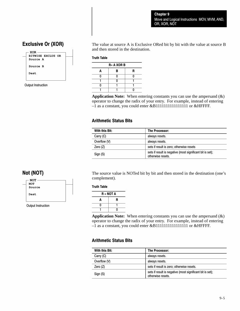
OR, XOR, NOT
Chapter 9
Move and Logical Instructions MOV, MVM, AND,
9–5
The value at source A is Exclusive ORed bit by bit with the value at source Band then stored in the destination.
Truth Table
R= A XOR B
A B R
0 0 0
1 0 1
0 1 1
1 1 0
Application Note: When entering constants you can use the ampersand (&)operator to change the radix of your entry. For example, instead of entering–1 as a constant, you could enter &B1111111111111111 or &HFFFF.
Arithmetic Status Bits
With this Bit: The Processor:
Carry (C) always resets.
Overflow (V) always resets.
Zero (Z) sets if result is zero; otherwise resets
Sign (S)sets if result is negative (most significant bit is set);otherwise resets.
The source value is NOTed bit by bit and then stored in the destination (one’scomplement).
Truth Table
R = NOT A
A R
0 1
1 0
Application Note: When entering constants you can use the ampersand (&)operator to change the radix of your entry. For example, instead of entering–1 as a constant, you could enter &B1111111111111111 or &HFFFF.
Arithmetic Status Bits
With this Bit: The Processor:
Carry (C) always resets.
Overflow (V) always resets.
Zero (Z) sets if result is zero; otherwise resets.
Sign (S)sets if result is negative (most significant bit is set);otherwise resets.
XORBITWISE EXCLUS ORSource A
Source B
Dest
Output Instruction
Exclusive Or (XOR)
NOTNOTSource
Dest
Output Instruction
Not (NOT)

10Chapter
10–1
File Copy and File Fill Instructions
This chapter covers the following instructions:
• File Copy (COP)• File Fill (FLL)
The destination file type determines the number of words that an instructiontransfers. For example, if the destination file type is counter and the sourcefile type is integer, three integer words are transferred for each element in thecounter-type file.
Effect on the Index Register in 5/02 and 5/03 Processors
After a COP or FLL instruction is executed, index register S:24 is cleared tozero.
This instruction copies data from one location into another. It uses no statusbits. If you need an enable bit, program a parallel output using a storageaddress. The following example shows how file instruction data ismanipulated.
Source Destination
File to File
Entering Parameters
Enter the following parameters when programming this instruction:
• Source is the address of the file you want to copy. You must use the fileindicator (#) in the address.
• Destination is the starting address where the instruction stores the copy.You must use the file indicator (#) in the address.
• Length is the number of elements in the file you want to copy. If thedestination file type is 3 words per element, you can specify a maximumlength of 42. If the destination file type is 1 word per element, you canspecify a maximum length of 128 words.
All elements are copied from the specified source file into the specifieddestination file each scan the rung is true. Elements are copied in ascendingorder with no transformation of data. They are copied up to the specified
File Copy and Fill InstructionsOverview
COPCOPY FILESourceDestLength
Output Instruction
File Copy (COP)

Instructions
Chapter 10
File Copy and File Fill
10–2
number (length) or until the last element of the destination file is reached,whichever occurs first.
If your destination is a timer, counter, or control file, be sure that the sourcewords corresponding to the status words of your destination file containszeros.
Be sure that you accurately specify the starting address and length of the datablock you are copying. The instruction will not write over a file boundary(such as between files N16 and N17) at the destination. An error occurs if awrite is attempted over a file boundary.
You can perform file shifts by specifying a source element address one ormore elements greater than the destination element address within the samefile. This shifts data to lower element addresses.
This instruction loads elements of a file with either a program constant or avalue from an element address. The following example shows how fileinstruction data is manipulated.
Source
Destination
Word to File
Entering Parameters
Enter the following parameters when programming this instruction:
• Source is the program constant or element address. The file indicator (#)is not required for an element address.
• Destination is the destination starting address of the file you want to fill.You must use the file indicator (#) in the address.
• Length is the number of elements in the file you want filled. If thedestination file type is 3 words per element, you can specify a maximumlength of 42. If the destination file type is 1 word per element, you canspecify a maximum length of 128 words.
All elements are filled from the source value (typically a program constant)into the specified destination file each scan the rung is true. Elements arefilled in ascending order until the number of elements (length that youentered) is reached.
The instruction will not write over a file boundary (such as between filesN16 and N17) at the destination. An error is declared if a write is attemptedover a file boundary.
FLLFILL FILESourceDestLength
Output Instruction
File Fill (FLL)

A–B 11Chapter
11–1
Bit Shift, FIFO, and LIFO Instructions
Use the following instructions with fixed, 5/01, 5/02, and 5/03 processors,except where noted.
If you want to: Use this instruction: Refer to page:
Load and unload data into a bitarray one bit at a time
BSL, BSR 2
Load and unload values in thesame order (first in first out)
FIFO (FFL, FFU)(5/02 and 5/03 only)
4
Load and unload values inreverse order (last in first out)
LIFO (LFL, LFU)(5/02 and 5/03 only)
6
FIFO instructions provide a method of loading words into a file andunloading them in the same order as they were loaded. The first word in isthe first word out.
LIFO instructions provide a method of loading words into a file andunloading them in the opposite order as they were loaded. The last word inis the first word out.
FIFO and LIFO instruction applications include assembly/transfer lines,inventory control, and system diagnostics.
The following general information applies to bit shift, FIFO, and LIFOinstructions.
Effect on the Index Register in 5/02 and 5/03 Processors
All of the instructions in this chapter alter the contents of the index register,S:24. Details appear with the instruction.
Bit Shift, FIFO, and LIFOInstructions Overview

Chapter 11
Bit Shift, FIFO, and LIFO Instructions
11–2
BSL and BSR are output instructions that load data into a bit array one bit ata time. The data is shifted through the array, then unloaded one bit at a time.
Entering Parameters
Enter the following parameters when programming these instructions:
• File is the address of the bit array you want to manipulate. You must usethe file indicator (#) in the bit array address.
• Control is the instruction’s address and control element that stores thestatus byte of the instruction, the size of the array (in number of bits), andthe bit pointer (currently not used). Note that the control address cannotbe used for any other instruction.
The control element is shown below.
EN DN ER UL Not used
15 13 11 10 00
Size of bit array (number of bits)
Bit Pointer (currently not used)
Word 0
Word 1
Word 2
Status bits of the control element include:
– Unload Bit UL (bit 10) stores the status of the bit exited from thearray each time the instruction is enabled.
– Error Bit ER (bit 11), when set, indicates the instruction detected anerror such as entering a negative number for the length or position.Avoid using the output bit when this bit is set.
– Done Bit DN (bit 13), when set, indicates the bit array has shiftedone position.
– Enable Bit EN (bit 15) is set on a false-to-true transition of the rungand indicates the instruction is enabled.
When the register shifts and input conditions go false, the enable, done,and error bits are reset.
• Bit Address is the address of the source bit that the instruction inserts inthe first bit location of the BSL array, or the last bit location of the BSRarray.
• Length (size of bit array) is the number of bits in the bit array, up to 2048bits. A length value of 0 causes the input bit to be transferred to the ULbit.A length value that points past the end of the programmed file causes aruntime major error to occur. If you alter a length value with your ladderprogram, make certain that the altered value is valid.
The instruction invalidates all bits beyond the last bit in the array (asdefined by the length) up to the next word boundary.
Effects on Index Register S:24
The shift operation clears the index register S:24 to zero.
(EN)(DN)
BSRBIT SHIFT RIGHTFile #B3:2Control R6:54Bit Address I:23/06Length 38
(EN)(DN)
BSLBIT SHIFT LEFTFile #B3:1Control R6:53Bit Address I:22/12Length 58
Output Instructions
Bit Shift Left and Bit Shift Right

Chapter 11
Bit Shift, FIFO, and LIFO Instructions
11–3
Operation – Bit Shift Left
When the rung goes from false–to–true, the enable bit (EN bit 15) is set andthe data block is shifted to the left (to a higher bit number) one bit position.The specified bit at the bit address is shifted into the first bit position. Thelast bit is shifted out of the array and stored in the unload bit (UL bit 10) inthe status byte of the control element. The shift is completed in one scan.
For wraparound operation, set the position of the bit address to the last bit ofthe array or to the UL bit, whichever applies.
The figure below illustrates how the Bit Shift Left instruction works.
(EN)(DN)
BSLBIT SHIFT LEFTFile #B3:1Control R6:53Bit Address I:22/12Length 58
19 18 17 16
35 34 33
51 50 49 48
67 66 65 64
32
23 22 21 20
39 38 37
55 54 53 52
71 70 69 68
36
27 26 25 24
43 42 41
59 58 57 56
73 72
40
31 30 29 28
47 46 45
63 62 61 60
44
INVALIDATED
58 Bit Array #B3:1
Source BitI:22/12
Unload Bit(R6:53/10)
Data block is shifted one bit at atime from bit 16 to bit 73.
Operation – Bit Shift Right
When the rung goes from false–to–true, the enable bit (EN bit 15) is set andthe data block is shifted to the right (to a lower bit number) one bit position.The specified bit at the bit address is shifted into the last bit position. Thefirst bit is shifted out of the array and stored in the unload bit (UL bit 10) inthe status byte of the control element. The shift is completed in one scan.
For wraparound operation, set the position of the bit address to the first bit ofthe array or to the UL bit, whichever applies.

Chapter 11
Bit Shift, FIFO, and LIFO Instructions
11–4
The figure below illustrates how the Bit Shift Right instruction works.
(EN)
(DN)
BSRBIT SHIFT RIGHTFile #B3:2Control R6:54Bit Address I:23/06Length 38
35 34 33
51 50 49 48
67 66 65 64
3239 38 37
55 54 53 52
69 68
3643 42 41
59 58 57 56
4047 46 45
63 62 61 60
44
INVALIDATED
38 Bit Array #B3:2
Source BitI:23/06
Unload Bit(R6:54/10)
Data block is shifted one bit at atime from bit 69 to bit 32.
If you wish to shift more than one bit per scan, you must create a loopconstruct using ladder logic.
FFL and FFU instructions are used in pairs. The FFL instruction loads wordsinto a user-created file called a FIFO stack. The FFU instruction unloadswords from the FIFO stack, in the same order as they were entered.
Entering Parameters
Enter the following parameters when programming these instructions:
• Source is a word address or program constant (–32768 to 32767) thatstores the value to be entered next into the FIFO stack. The FFLinstruction places this value into the next available element in the FIFOstack.
• Destination (Dest) is a word address that stores the value which exitsfrom the FIFO stack. The FFU instruction unloads this value from thestack and places it in this word address.
• FIFO is the address of the stack. It must be an indexed word address inthe input, output, status, bit, or integer file. The same address isprogrammed for the FFL and FFU instructions.
• Length is the maximum number of elements in the stack, up to amaximum of 128 words. The same number is programmed for the FFLand FFU instructions.
• Position is the next available location where the instruction loads datainto the stack. This value changes after each load or unload operation.The same number is used for the FFL and FFU instructions.
(EN)(DN)(EM)
FFLFIFO LOADSourceFIFOControlLengthPosition
(EU)(DN)(EM)
FFUFIFO UNLOADFIFODestControlLengthPosition
Output Instructions
FIFO Load (FFL)FIFO Unload (FFU)

Chapter 11
Bit Shift, FIFO, and LIFO Instructions
11–5
• Control is a control file address. The status bits, the stack length, and theposition value are stored in this element. The same address isprogrammed for the FFL and FFU instructions. Do not use the controlfile address for any other instruction.The 3-word control element is shown below:
EN EU DN EM
15 14 13 12 11 10 09 08 07 06 05 04 03 02 01 00
Length
Position
Word 0
Word 1
Word 2
Status bits of the control element include:
– Empty Bit EM (bit 12) is set by the FFU instruction to indicate thestack is empty.
– Done Bit DN (bit 13) is set by the FFL instruction to indicate thestack is full. This inhibits loading the stack.
– FFU Enable Bit EU (bit 14) is set on a false-to-true transition of theFFU rung and is reset on a true-to-false transition.
– FFL Enable Bit EN (bit 15) is set on a false-to-true transition of theFFL rung and is reset on a true-to-false transition.
Operation
Instruction parameters have been programmed in the FFL – FFU instructionpair shown below.
(EN)(DN)(EM)
FFLFIFO LOADSource N7:10FIFO #N7:12Control R6:0Length 34Position 9
(EU)(DN)(EM)
FFUFIFO UNLOADFIFO #N7:12Dest N7:11Control R6:0Length 34Position 9
FFU instruction unloadsdata from stack #N7:12 atposition 0, N7:12.
N7:12 0
N7:13 1
N7:14 2
3
4
5
6
7
8
9
33
34 words areallocated for FIFOstack starting atN7:12, ending atN7:45.
FFL-FFU Instruction Pair
Loading and Unloading of Stack #N7:12
N7:10
N7:11
PositionDestination
Source
FFL instruction loads datainto stack #N7:12 at thenext available position, 9 inthis case.
N7:45
FFL Instruction Operation: When rung conditions change fromfalse–to–true, the FFL enable bit (EN) is set. This loads the contents of theSource, N7:10, into the stack element indicated by the Position number, 9.The position value then increments.The FFL instruction loads an element at each false–to–true transition of therung, until the stack is filled (34 elements). The done bit (DN) is then set,which inhibits further loading.
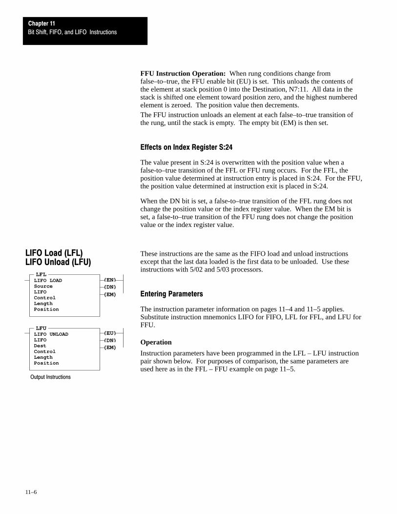
Chapter 11
Bit Shift, FIFO, and LIFO Instructions
11–6
FFU Instruction Operation: When rung conditions change fromfalse–to–true, the FFU enable bit (EU) is set. This unloads the contents ofthe element at stack position 0 into the Destination, N7:11. All data in thestack is shifted one element toward position zero, and the highest numberedelement is zeroed. The position value then decrements.The FFU instruction unloads an element at each false–to–true transition ofthe rung, until the stack is empty. The empty bit (EM) is then set.
Effects on Index Register S:24
The value present in S:24 is overwritten with the position value when afalse-to–true transition of the FFL or FFU rung occurs. For the FFL, theposition value determined at instruction entry is placed in S:24. For the FFU,the position value determined at instruction exit is placed in S:24.
When the DN bit is set, a false-to–true transition of the FFL rung does notchange the position value or the index register value. When the EM bit isset, a false-to–true transition of the FFU rung does not change the positionvalue or the index register value.
These instructions are the same as the FIFO load and unload instructionsexcept that the last data loaded is the first data to be unloaded. Use theseinstructions with 5/02 and 5/03 processors.
Entering Parameters
The instruction parameter information on pages 11–4 and 11–5 applies.Substitute instruction mnemonics LIFO for FIFO, LFL for FFL, and LFU forFFU.
Operation
Instruction parameters have been programmed in the LFL – LFU instructionpair shown below. For purposes of comparison, the same parameters areused here as in the FFL – FFU example on page 11–5.
(EN)(DN)(EM)
LFLLIFO LOADSourceLIFOControlLengthPosition
(EU)(DN)(EM)
LFULIFO UNLOADLIFODestControlLengthPosition
Output Instructions
LIFO Load (LFL)LIFO Unload (LFU)

Chapter 11
Bit Shift, FIFO, and LIFO Instructions
11–7
(EN)(DN)(EM)
LFLLIFO LOADSource N7:10LIFO #N7:12Control R6:0Length 34Position 9
(EU)(DN)(EM)
LFULIFO UNLOADLIFO #N7:12Dest N7:11Control R6:0Length 34Position 9
LFU instruction unloadsdata from stack #N7:12 atposition 8.
N7:12 0
N7:13 1
N7:14 2
3
4
5
6
7
8
9
33
34 words areallocated for LIFOstack starting atN7:12, ending atN7:45.
Loading and Unloading of Stack #N7:12
N7:10
N7:11
Position
Destination
Source
LFL instruction loads datainto stack #N7:12 at thenext available position, 9 inthis case.
LFL-LFU Instruction PairN7:45
LFL Instruction Operation: When rung conditions change fromfalse–to–true, the LFL enable bit (EN) is set. This loads the contents of theSource, N7:10, into the stack element indicated by the Position number, 9.The position value then increments.The LFL instruction loads an element at each false–to–true transition of therung, until the stack is filled (34 elements). The done bit (DN) is then set,which inhibits further loading.
LFU Instruction Operation: When rung conditions change fromfalse–to–true, the LFU enable bit (EU) is set. This unloads data from the lastelement loaded into the stack (at the position value minus 1), placing it in theDestination, N7:11. The position value then decrements.The LFU instruction unloads one element at each false–to–true transition ofthe rung, until the stack is empty. The empty bit (EM) is then set.
Effects on Index Register S:24
The value present in S:24 is overwritten with the position value when afalse–to–true transition of the LFL or LFU rung occurs. For the LFL, theposition value determined at instruction entry is placed in S:24. For theLFU, the position value determined at instruction exit is placed in S:24.
When the DN bit is set, a false-to–true transition of the LFL rung does notchange the position value or the index register value. When the EM bit isset, a false–to–true transition of the LFU rung does not change the positionvalue or the index register value.

A–B 12Chapter
12–1
Sequencer Instructions
The following instructions are generally used in machine control. Use theseinstructions with fixed, 5/01, 5/02, and 5/03 processors, except where noted.
If you want to: Use this instruction: Refer to page:
Transfer 16-bit data to wordaddresses
SQO 2
Compare 16-bit data withstored data
SQC 2
Load 16-bit data into a file SQL (5/02 and 5/03 only) 7
The following general information applies to sequencer instructions.
Applications Requiring More than 16-Bits
When your application requires more than 16–bits, use parallel multiplesequencer instructions.
Effect on the Index Register in 5/02 and 5/03 Processors
Sequencer instructions alter the contents of the index register (S:24). Detailsappear with the specific instructions.
Sequencer InstructionsOverview
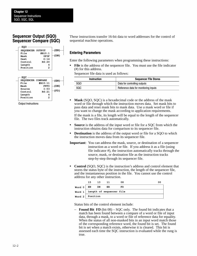
SQO, SQC, SQL
Chapter 12
Sequencer Instructions
12–2
These instructions transfer 16-bit data to word addresses for the control ofsequential machine operations.
Entering Parameters
Enter the following parameters when programming these instructions:
• File is the address of the sequencer file. You must use the file indicator(#) for this address.Sequencer file data is used as follows:
Instruction Sequencer File Stores
SQO Data for controlling outputs
SQC Reference data for monitoring inputs
• Mask (SQO, SQC) is a hexadecimal code or the address of the maskword or file through which the instruction moves data. Set mask bits topass data and reset mask bits to mask data. Use a mask word or file ifyou want to change the mask according to application requirements.If the mask is a file, its length will be equal to the length of the sequencerfile. The two files track automatically.
• Source is the address of the input word or file for a SQC from which theinstruction obtains data for comparison to its sequencer file.
• Destination is the address of the output word or file for a SQO to whichthe instruction moves data from its sequencer file.
Important : You can address the mask, source, or destination of a sequencerinstruction as a word or file. If you address it as a file (usingfile indicator #), the instruction automatically tracks through thesource, mask, or destination file as the instruction tracksstep-by-step through its sequencer file.
• Control (SQO, SQC) is the instruction’s address and control element thatstores the status byte of the instruction, the length of the sequencer file,and the instantaneous position in the file. You cannot use the controladdress for any other instruction.
EN DN ER FD
15 13 11 08 00
Length of sequencer file
Position
Word 0
Word 1
Word 2
Status bits of the control element include:
– Found Bit FD (bit 08) – SQC only. The found bit indicates that amatch has been found between a compare of a word or file of inputdata, through a mask, to a word or file of reference data for equality.When the status of all non-masked bits in an input word match thoseof the corresponding reference word, the found bit is set. The foundbit is set when a match exists, otherwise it is cleared. This bit isassessed each time the SQC instruction is evaluated while the rung istrue.
SQOSEQUENCER OUTPUTFile #B10:1Mask 0F0FDest O:14Control R6:20Length 4Position 2
(EN)
(DN)
SQCSEQUENCER COMPAREFile #B10:11Mask FFF0Source I:03Control R6:21Length 4Position 2
(FD)
(EN)
(DN)
Output Instructions
Sequencer Output (SQO)Sequencer Compare (SQC)

SQO, SQC, SQL
Chapter 12
Sequencer Instructions
12–3
– Error Bit ER (bit 11) is set when the processor detects a negativeposition value, or a negative or zero length value. This results in amajor error if not cleared before the END or TND instruction isexecuted.
– Done Bit DN (bit 13) is set by the SQO or SQC instruction after ithas operated on the last word in the sequencer file. It is reset on thenext false-to-true rung transition after the rung goes false.
– Enable EN (bit 15) is set by a false-to-true rung transition andindicates the SQO or SQC instruction is enabled. It follows the rungcondition.
• Length is the number of steps of the sequencer file starting at position 1.The maximum number you can enter is 255 words. Position 0 is thestartup position. The instruction resets (wraps) to position 1 at each cyclecompletion.The address assigned for a sequencer file is step zero. Sequencerinstructions use length + 1 word of data table files for each file referencedin the instruction. This applies to the source, mask, and/or destination ifaddressed as files.A length value that points past the end of the programmed file causes aruntime major error to occur. If you alter a length value with your ladderprogram, make certain that the altered value is valid.
• Position is the word location or step in the sequencer file from/to whichthe instruction moves data.A position value that points past the end of the programmed file causes aruntime major error to occur. If you alter a position value with yourladder program, make certain that the altered value is valid.
Application Note: You may use the reset (RES) instruction to reset asequencer. All control bits (except FD) will be reset to zero. The Positionwill also be set to zero. Program the address of your control register in theRES (R6:0).
Operation – Sequencer Output
This output instruction steps through the sequencer file whose bits have beenset to control various output devices.
When the rung goes from false–to–true, the instruction increments to the nextstep (word) in the sequencer file. Data stored there is transferred through amask to the destination address specified in the instruction. Current data iswritten to the corresponding destination word every scan that the rungremains true.
The done bit is set when the last word of the sequencer file is transferred. Onthe next false-to-true rung transition, the instruction resets the position to stepone.

SQO, SQC, SQL
Chapter 12
Sequencer Instructions
12–4
If the position is equal to zero at startup, when you switch the processor fromthe program mode to the run mode instruction operation depends on whetherthe rung is true or false on the first scan.
• If true, the instruction transfers the value in step zero.• If false, the instruction waits for the first rung transition from
false–to–true and transfers the value in step one.
Mask data by resetting bits in the mask word. The bits mask data when reset,pass data when set. Unless you set mask bits, the instruction will not changethe value in the destination word. The mask can be fixed by entering ahexadecimal code. The mask can be a variable by entering an elementaddress or a file address for changing the mask with each step.
The following figure indicates how the SQO instruction works.
SQOSEQUENCER OUTPUTFile #B10:1Mask 0F0FDest O:14.0Control R6:20Length 4Position 2
(EN)
(DN)
0000 0101 0000 1010
07 815
0000 1111 0000 1111
07 815
0000 0000 0000 0000
1010 0010 1111 0101
1111 0101 0100 1010
0101 0101 0101 0101
0000 1111 0000 1111
0
1
2
3
4
Step
B10:1
2
3
4
5
Word
00010203040506070809101112131415
ON
ON
ON
ON
External OutputsAssociated with O:14
Destination O:14.0
Mask Value 0F0F
Sequencer Output File #B10:1
Current Step
Effects on Index Register S:24
The value present in the index register S:24 is overwritten when thesequencer output instruction is true. The index register value will equal theposition value of the instruction.

SQO, SQC, SQL
Chapter 12
Sequencer Instructions
12–5
Operation – Sequencer Compare
The SQC instruction compares a word or file of input data, through a mask,to a word or file of reference data for equality. When the status of allnon-masked bits in an input word match those of the corresponding referenceword, the instruction becomes true and sets the found bit (FD) in therespective control word. Otherwise, the instruction is false, which clears thefound bit (FD).
Mask data by resetting bits in the mask word. The bits mask data when resetand pass data when set. Unless you set mask bits, the instruction does notcompare bits in the reference file against the input value. The mask can befixed by entering a hex code. The mask can be a variable by entering anelement address or a file address for changing the mask at each step.
When the rung goes from false–to–true, the instruction increments to the nextstep (word) in the sequencer file. Data stored there is transferred through amask and compared against the source data for equality. If the source dataequals the reference data, the FD bit is set in the SQC’s control counter.Current data is compared against the source every scan that the rungevaluates as true.
Applications of the SQC instruction include machine diagnostics. Thefollowing figure explains how the SQC instruction works.
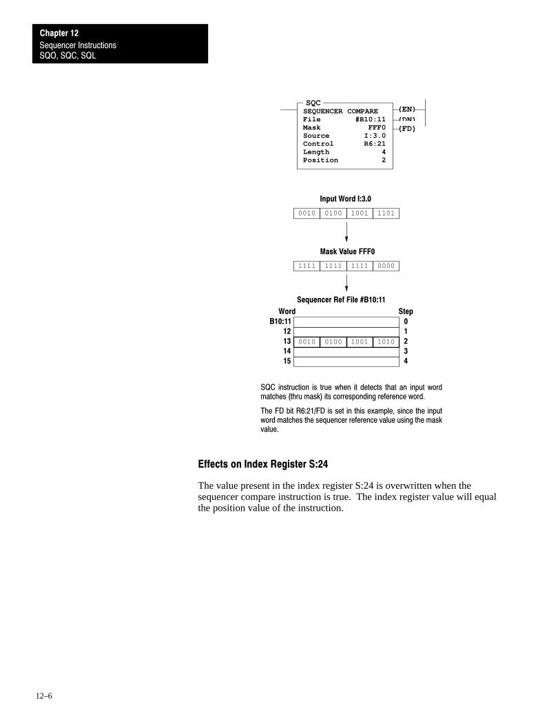
SQO, SQC, SQL
Chapter 12
Sequencer Instructions
12–6
0010 0100 1001 1101
1111 1111 1111 0000
0010 0100 1001 1010
0
1
2
3
4
Step
B10:11
12
13
14
15
Word
Input Word I:3.0
Mask Value FFF0
Sequencer Ref File #B10:11
(EN)(DN)
SQCSEQUENCER COMPAREFile #B10:11Mask FFF0Source I:3.0Control R6:21Length 4Position 2
(FD)
SQC instruction is true when it detects that an input wordmatches (thru mask) its corresponding reference word.
The FD bit R6:21/FD is set in this example, since the inputword matches the sequencer reference value using the maskvalue.
Effects on Index Register S:24
The value present in the index register S:24 is overwritten when thesequencer compare instruction is true. The index register value will equalthe position value of the instruction.
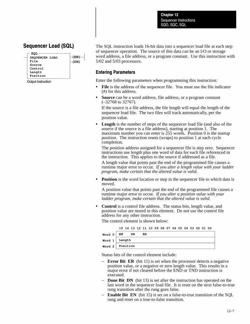
SQO, SQC, SQL
Chapter 12
Sequencer Instructions
12–7
The SQL instruction loads 16-bit data into a sequencer load file at each stepof sequencer operation. The source of this data can be an I/O or storageword address, a file address, or a program constant. Use this instruction with5/02 and 5/03 processors.
Entering Parameters
Enter the following parameters when programming this instruction:
• File is the address of the sequencer file. You must use the file indicator(#) for this address.
• Source can be a word address, file address, or a program constant(–32768 to 32767).If the source is a file address, the file length will equal the length of thesequencer load file. The two files will track automatically, per theposition value.
• Length is the number of steps of the sequencer load file (and also of thesource if the source is a file address), starting at position 1. Themaximum number you can enter is 255 words. Position 0 is the startupposition. The instruction resets (wraps) to position 1 at each cyclecompletion.The position address assigned for a sequencer file is step zero. Sequencerinstructions use length plus one word of data for each file referenced inthe instruction. This applies to the source if addressed as a file.A length value that points past the end of the programmed file causes aruntime major error to occur. If you alter a length value with your ladderprogram, make certain that the altered value is valid.
• Position is the word location or step in the sequencer file to which data ismoved.A position value that points past the end of the programmed file causes aruntime major error to occur. If you alter a position value with yourladder program, make certain that the altered value is valid.
• Control is a control file address. The status bits, length value, andposition value are stored in this element. Do not use the control fileaddress for any other instruction.The control element is shown below:
EN DN ER
15 14 13 12 11 10 09 08 07 06 05 04 03 02 01 00
Length
Position
Word 0
Word 1
Word 2
Status bits of the control element include:
– Error Bit ER (bit 11) is set when the processor detects a negativeposition value, or a negative or zero length value. This results in amajor error if not cleared before the END or TND instruction isexecuted.
– Done Bit DN (bit 13) is set after the instruction has operated on thelast word in the sequencer load file. It is reset on the next false-to-truerung transition after the rung goes false.
– Enable Bit EN (bit 15) is set on a false-to-true transition of the SQLrung and reset on a true-to-false transition.
(EN)(DN)
SQLSEQUENCER LOADFileSourceControlLengthPosition
Output Instruction
Sequencer Load (SQL)

SQO, SQC, SQL
Chapter 12
Sequencer Instructions
12–8
Operation
Instruction parameters have been programmed in the SQL instruction shownbelow. Input word I:1.0 is the source. Data in this word is loaded intointeger file #N7:30 by the sequencer load instruction.
(EN)
(DN)
SQLSEQUENCER LOADFile #N7:30Source I:1.0Control R6:4Length 4Position 2
0000 0101 0000 1010
07 815
0000 0000 0000 0000
1010 0010 1111 0101
0000 0101 0000 1010
0000 0000 0000 0000
0000 0000 0000 0000
0
1
2
3
4
Step
N7:30
31
32
33
34
Word
00010203040506070809101112131415
ON
ON
ON
ON
External InputsAssociated with I:1.0
Source I:1.0
Sequencer Load File #N7:30
Current Step
When rung conditions change from false–to–true, the SQL enable bit (EN) isset. The control element R6:4 increments to the next position in thesequencer file, and loads the contents of source I:1.0 into this location. TheSQL instruction continues to load the current data into this location each scanthat the rung remains true. When the rung goes false, the enable bit (EN) isreset.
The instruction loads data into a new file element at each false–to–truetransition of the rung. When step 4 is completed, the done bit (DN) is set.Operation cycles to position 1 at the next false–to–true transition of the rungafter position 4.
If the source were a file address such as #N7:40, files #N7:40 and #N7:30would both have a length of 5 (0–4) and would track through the stepstogether per the position value.
Effects on Index Register S:24
The value present in the index register S:24 is overwritten when thesequencer load instruction is true. The index register value will equal theposition value of the instruction.

A–B 13Chapter
13–1
Control Instructions
Control instructions allow you to change the order in which the processorscans a ladder program. Typically, these instructions are used to minimizescan time, create a more efficient program, and to troubleshoot a ladderprogram. Use the following control instructions with fixed, 5/01, 5/02, and5/03 processors, except where noted.
If you want to: Use this instruction Refer to page:
Jump forward or backward to acorresponding label instruction
JMP, LBL 1
Jump to a designatedsubroutine and return
JSR, SBR, RET 2, 3, 4
Enable or inhibit a mastercontrol zone in your ladderprogram
MCR 4
Truncate program scan TND 5
Debug or diagnose your userprogram
SUS 5
Program an interrupt label INT (5/02 and 5/03 only) 6
When the rung condition for this output instruction is true, the processorjumps forward or backward to the corresponding label instruction (LBL) andresumes program execution at the label. More than one JMP instruction canjump to the same label.
Important: Be careful when using the JMP instruction to move backwardsor loop through your program. If you loop too many times, youmay cause the watchdog timer to time out and fault theprocessor. Use a counter, timer, or the “program scan” register(system status register, word S:3, bits 0–7) to limit the amountof time you spend looping inside of JMP/LBL instructions.
Entering Parameters
Enter a decimal label number from 0 to 999. Up to 1,000 labels are allowedper program or subroutine file.
(JMP)
Output Instruction
Jump to Label (JMP)

RET, MCR, TND, SUS, INT, STI
Chapter 13
Control Instructions JMP, LBL, JSR, SBR
13–2
This input instruction is the target of the JMP instruction having the samelabel number. You must program this instruction as the first instruction of arung. This instruction has no control bits. It is always evaluated as true orlogic 1.
You can program multiple jumps to the same label by assigning the samelabel number to multiple JMP instructions, but assigning the same labelnumber to two or more labels causes a compile time error.
Important: Do not jump (JMP) into an MCR zone. Instructions that areprogrammed within the MCR zone starting at the LBLinstruction and ending at the ‘END MCR’ instruction willalways be evaluated as though the MCR zone is true,irregardless of the true state of the “Start MCR” instruction.
Entering Parameters
Enter a decimal label number from 0 to 999. You can place up to 1,000labels in your program or subroutine file.
When the rung condition for a JSR instruction is true, the processor jumps tothe subroutine instruction (SBR) at the beginning of the target subroutine fileand resumes execution at that point. You cannot jump into any part of asubroutine except the first instruction in that file.
You must program each subroutine in its own program file by assigning aunique file number (3–255).
Fixed and 5/01 specific – The JSR instruction should not be programmed innested output branches.
Nesting Subroutine Files
Nesting subroutines allow you to direct program flow from the main programto a subroutine and then on to another subroutine. The following rules applywhen nesting subroutines:
• With fixed and 5/01 processors, you can nest subroutines up to fourlevels.
• With 5/02 and 5/03 processors, you can nest subroutines up to eightlevels. If you are using an STI subroutine, I/O event–driven interruptsubroutine, or user fault routine, you can nest subroutines up to threelevels from each subroutine.
A compiler error will occur if a rung containing multiple outputs withconditional logic and a JSR instruction is encountered.
]LBL[
Input Instruction
Label (LBL)
JSRJUMP TO SUBROUTINESBR file number
Output Instruction
Jump to Subroutine (JSR)

RET, MCR, TND, SUS, INT, STI
Chapter 13
Control Instructions JMP, LBL, JSR, SBR,
13–3
The following example illustrates jumping to successive subroutines, thenreturning in reverse order.
JSR
90
JSR
91
SBR
RET
SBR SBR
JSR
92
RET RET
Example of Nesting Subroutines to Level 3
Program
Main
Subroutine File 90
Level 1
Subroutine File 91
Level 2
Subroutine File 92
Level 3
Runtime errors occur if more than the allowable levels of subroutines arecalled (subroutine stack overflow) or if more returns are executed than thereare call levels (subroutine stack underflow). Also, do not execute a JSR to asubroutine that is already active in the subroutine stack.
Update critical I/O in subroutines using immediate input and/or outputinstructions, especially if your application calls for nested or relatively longsubroutines. Otherwise, the processor does not update I/O until it reaches theend of the main program after executing subroutines.
Entering Parameters
Enter a decimal subroutine number from 3 to 255.
The target subroutine is identified by the file number that you entered in theJSR instruction. The instruction serves as a label or identifier for a programfile as a regular subroutine file.
This instruction has no control bits. It is always evaluated as true. Theinstruction must be programmed as the first instruction of the first rung of asubroutine. Use of this instruction is optional; however, we recommendusing it.
SBRSUBROUTINE
Input Instruction
Subroutine (SBR)
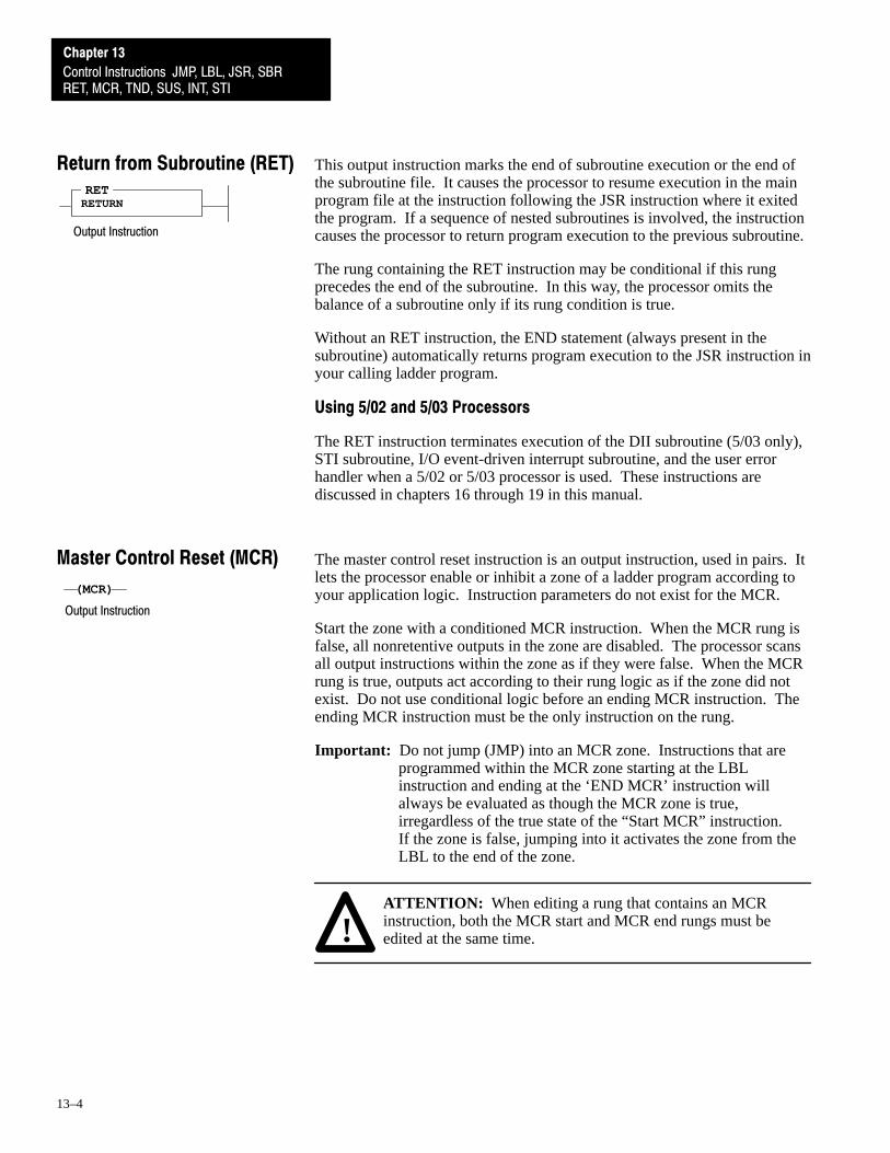
RET, MCR, TND, SUS, INT, STI
Chapter 13
Control Instructions JMP, LBL, JSR, SBR
13–4
This output instruction marks the end of subroutine execution or the end ofthe subroutine file. It causes the processor to resume execution in the mainprogram file at the instruction following the JSR instruction where it exitedthe program. If a sequence of nested subroutines is involved, the instructioncauses the processor to return program execution to the previous subroutine.
The rung containing the RET instruction may be conditional if this rungprecedes the end of the subroutine. In this way, the processor omits thebalance of a subroutine only if its rung condition is true.
Without an RET instruction, the END statement (always present in thesubroutine) automatically returns program execution to the JSR instruction inyour calling ladder program.
Using 5/02 and 5/03 Processors
The RET instruction terminates execution of the DII subroutine (5/03 only),STI subroutine, I/O event-driven interrupt subroutine, and the user errorhandler when a 5/02 or 5/03 processor is used. These instructions arediscussed in chapters 16 through 19 in this manual.
The master control reset instruction is an output instruction, used in pairs. Itlets the processor enable or inhibit a zone of a ladder program according toyour application logic. Instruction parameters do not exist for the MCR.
Start the zone with a conditioned MCR instruction. When the MCR rung isfalse, all nonretentive outputs in the zone are disabled. The processor scansall output instructions within the zone as if they were false. When the MCRrung is true, outputs act according to their rung logic as if the zone did notexist. Do not use conditional logic before an ending MCR instruction. Theending MCR instruction must be the only instruction on the rung.
Important: Do not jump (JMP) into an MCR zone. Instructions that areprogrammed within the MCR zone starting at the LBLinstruction and ending at the ‘END MCR’ instruction willalways be evaluated as though the MCR zone is true,irregardless of the true state of the “Start MCR” instruction. If the zone is false, jumping into it activates the zone from theLBL to the end of the zone.
!ATTENTION: When editing a rung that contains an MCRinstruction, both the MCR start and MCR end rungs must beedited at the same time.
RETRETURN
Output Instruction
Return from Subroutine (RET)
(MCR)
Output Instruction
Master Control Reset (MCR)
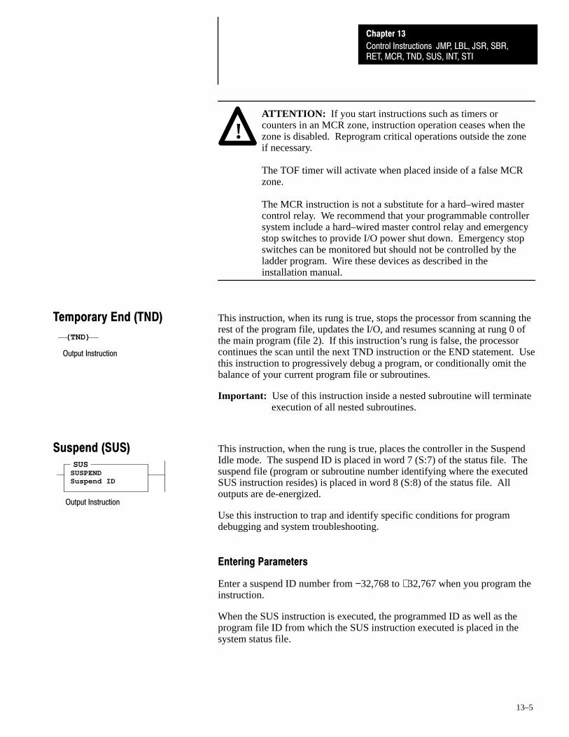
RET, MCR, TND, SUS, INT, STI
Chapter 13
Control Instructions JMP, LBL, JSR, SBR,
13–5
!ATTENTION: If you start instructions such as timers orcounters in an MCR zone, instruction operation ceases when thezone is disabled. Reprogram critical operations outside the zoneif necessary.
The TOF timer will activate when placed inside of a false MCRzone.
The MCR instruction is not a substitute for a hard–wired mastercontrol relay. We recommend that your programmable controllersystem include a hard–wired master control relay and emergencystop switches to provide I/O power shut down. Emergency stopswitches can be monitored but should not be controlled by theladder program. Wire these devices as described in theinstallation manual.
This instruction, when its rung is true, stops the processor from scanning therest of the program file, updates the I/O, and resumes scanning at rung 0 ofthe main program (file 2). If this instruction’s rung is false, the processorcontinues the scan until the next TND instruction or the END statement. Usethis instruction to progressively debug a program, or conditionally omit thebalance of your current program file or subroutines.
Important: Use of this instruction inside a nested subroutine will terminateexecution of all nested subroutines.
This instruction, when the rung is true, places the controller in the SuspendIdle mode. The suspend ID is placed in word 7 (S:7) of the status file. Thesuspend file (program or subroutine number identifying where the executedSUS instruction resides) is placed in word 8 (S:8) of the status file. Alloutputs are de-energized.
Use this instruction to trap and identify specific conditions for programdebugging and system troubleshooting.
Entering Parameters
Enter a suspend ID number from −32,768 to +32,767 when you program theinstruction.
When the SUS instruction is executed, the programmed ID as well as theprogram file ID from which the SUS instruction executed is placed in thesystem status file.
(TND)
Output Instruction
Temporary End (TND)
SUSSUSPENDSuspend ID
Output Instruction
Suspend (SUS)

RET, MCR, TND, SUS, INT, STI
Chapter 13
Control Instructions JMP, LBL, JSR, SBR
13–6
The Selectable Timed Interrupt function allows you to interrupt the scan ofthe main program file automatically, on a periodic basis, in order to scan aspecified subroutine file. Use these instructions with 5/02 and 5/03processors.
Important: The information here is for reference only. Program theseinstructions using the information appearing in chapter 18 ofthis manual.
Selectable Timed Interrupt Disable and Enable (STD, STE)
These instructions are generally used in pairs. The purpose is to prevent theSTI from occurring during a portion of the ladder program.
Selectable Timed Interrupt Start (STS)
The Selectable Timed Start (STS) function is used to initiate or restart theSTI function. Instruction parameters are the STI file number and the STIsetpoint.
This instruction serves as a label or identifier of a program file as an interruptsubroutine (INT label) versus a regular subroutine (SBR label). It can beused to identify Selectable Timed interrupts or I/O event–driven interrupts.Use this instruction with 5/02 and 5/03 processors.
This instruction has no control bits and is always evaluated as true. Theinstruction must be programmed as the first instruction of the first rung of thesubroutine. Use of this instruction is optional; however, we recommendusing it.
Selectable Timed Interrupts
STDSELECTABLE TIMED DISABLE
STESELECTABLE TIMED ENABLE
Output Instructions
STSSELECTABLE TIMED STARTFileTime (x10 ms)
Output Instruction
INTERRUPT SUBROUTINE
Input Instruction
INT
Interrupt Subroutine (INT)

A–B 14Chapter
14–1
Proportional Integral Derivative Instruction
This chapter describes the Proportional Integral Derivative (PID) instruction.This instruction applies to 5/02 and 5/03 processors.
This is an output instruction that controls physical properties such astemperature, pressure, liquid level, or flow rate using process loops.
The PID instruction normally controls a closed loop using inputs from ananalog input module and providing an output to an analog output module.For temperature control, you can convert the analog output to a timeproportioning on/off output for driving a heater or cooling unit. An exampleappears on pages 14–11 through 14–13.
The PID instruction can be operated in the timed mode or the STI mode. Inthe timed mode, the instruction updates its output periodically at auser-selectable rate. In the STI mode, the instruction should be placed in anSTI interrupt subroutine. It then updates its output every time the STIsubroutine is scanned. The STI time interval and the PID loop update ratemust be the same in order for the equation to execute properly.
PID closed loop control holds a process variable at a desired set point. Aflow rate/fluid level example is shown below.
∑ ∑PID
Equation
Feed Forward
or Bias
Control
Output
Level
Detector
Process
Variable
ErrorSet Point
Flow Rate
Control Valve
The PID equation controls the process by sending an output signal to thecontrol valve. The greater the error between the setpoint and processvariable input, the greater the output signal, and vice versa. An additionalvalue (feedforward or bias) can be added to the control output as an offset.The result of PID calculation (control variable) will drive the processvariable you are controlling toward the set point.
PIDPIDControl BlockProcess VariableControl VariableControl Block Length 23
Output Instruction
PID Overview
The PID Concept
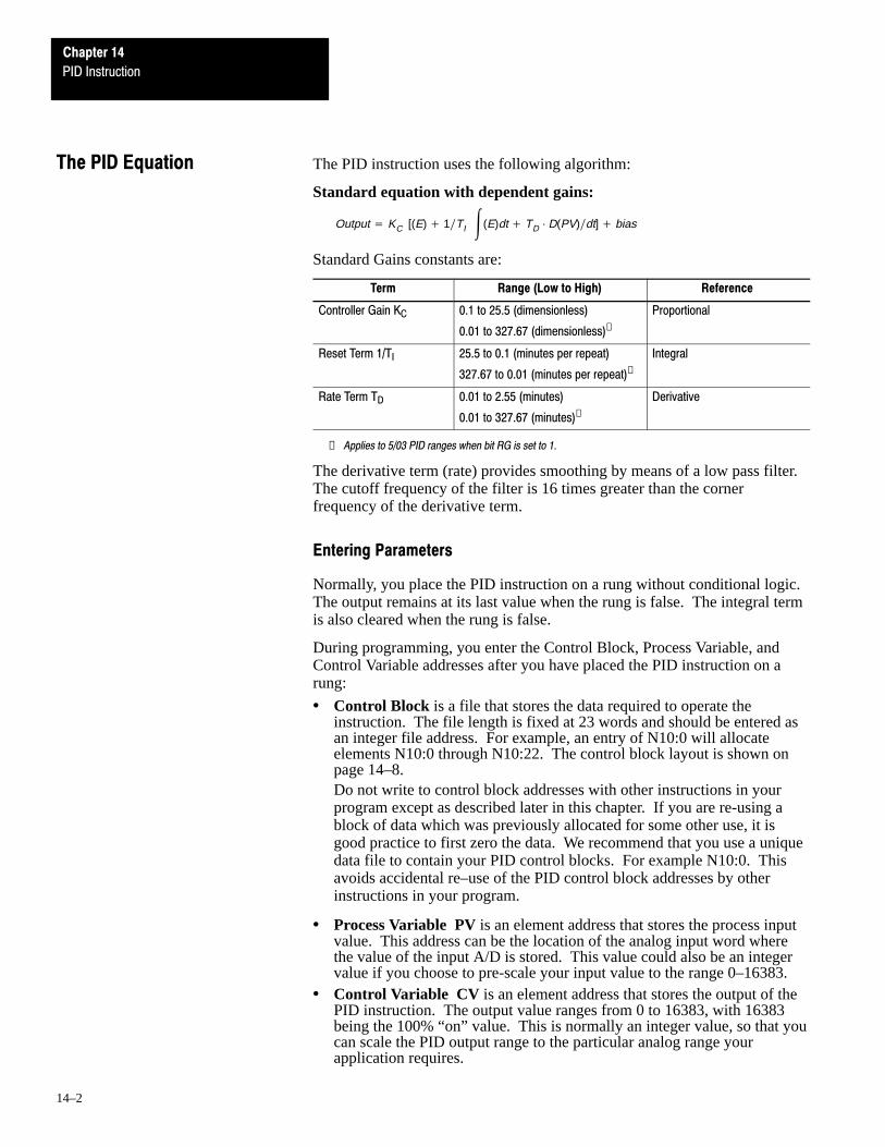
Chapter 14
PID Instruction
14–2
The PID instruction uses the following algorithm:
Standard equation with dependent gains:
Output � KC [(E) � 1�TI �(E)dt � TD · D(PV)�dt] � bias
Standard Gains constants are:
Term Range (Low to High) Reference
Controller Gain KC 0.1 to 25.5 (dimensionless)
0.01 to 327.67 (dimensionless)➀
Proportional
Reset Term 1/TI 25.5 to 0.1 (minutes per repeat)
327.67 to 0.01 (minutes per repeat)➀
Integral
Rate Term TD 0.01 to 2.55 (minutes)
0.01 to 327.67 (minutes)➀
Derivative
➀ Applies to 5/03 PID ranges when bit RG is set to 1.
The derivative term (rate) provides smoothing by means of a low pass filter.The cutoff frequency of the filter is 16 times greater than the cornerfrequency of the derivative term.
Entering Parameters
Normally, you place the PID instruction on a rung without conditional logic.The output remains at its last value when the rung is false. The integral termis also cleared when the rung is false.
During programming, you enter the Control Block, Process Variable, andControl Variable addresses after you have placed the PID instruction on arung:
• Control Block is a file that stores the data required to operate theinstruction. The file length is fixed at 23 words and should be entered asan integer file address. For example, an entry of N10:0 will allocateelements N10:0 through N10:22. The control block layout is shown onpage 14–8.Do not write to control block addresses with other instructions in yourprogram except as described later in this chapter. If you are re-using ablock of data which was previously allocated for some other use, it isgood practice to first zero the data. We recommend that you use a uniquedata file to contain your PID control blocks. For example N10:0. Thisavoids accidental re–use of the PID control block addresses by otherinstructions in your program.
• Process Variable PV is an element address that stores the process inputvalue. This address can be the location of the analog input word wherethe value of the input A/D is stored. This value could also be an integervalue if you choose to pre-scale your input value to the range 0–16383.
• Control Variable CV is an element address that stores the output of thePID instruction. The output value ranges from 0 to 16383, with 16383being the 100% “on” value. This is normally an integer value, so that youcan scale the PID output range to the particular analog range yourapplication requires.
The PID Equation

Chapter 14
PID Instruction
14–3
The figure below shows a PID instruction with typical addresses for theseparameters entered:
PIDPIDControl Block N10:0Process Variable N10:28Control Variable N10:29Control Block Length 23
After you enter the Control Block, Process Variable, and Control Variableaddresses, the APS software displays the following data entry screen. Anasterisk (∗) denotes that you can not cursor to the field.
F1 auto/manual: MANUAL ∗ time mode Bit: 1 TMF2 mode: TIMED ∗ auto/manual bit: 1 AMF3 control: E=SP–PV ∗ control mode bit: 0 CM
setpoint (SP): 0 output limiting enabled bit: 0 OLprocess (PV): 0 ∗ reset and gain range: 0 RGscaled error: 0 ∗ scale setpoint flag: 0 SC
deadband: 0 loop update time too fast: 0 TFoutput (CV): 0 % ∗ derivitive (rate) action: 0 DA
DB, set when error is in DB: 0 DBloop update: 0 [.01 secs] output alarm, upper limit: 0 UL
gain: 0 [/10] output alarm, lower limit: 0 LLreset: 0 [/10 m/r] setpoint out of range: 0 SP
rate: 0 [/100 min] process var out of range: 0 PVmin scaled: 0 PID done: 0 DNmax scaled: 0
F4 output (CV) limit: NO ∗ PID enabled: 0 ENoutput (CV) min: 0 %output (CV) max: 0 %
Enter value or press <ESC> to exitN10:4 =offline no forces INSTR INSERT File PIDS
Message:Prompt:Data/Cmd Entry:Status:
Main Functions:
Display Area:
F1 F3 F4F2
TOGGLEAUTO/MN
TOGGLECONTROL
TOGGLEOUT LIM
TOGGLEMODE
The left column in the display above lists further PID instruction parametersyou must enter.
• [F1] Auto/Manual AM (word 0, bit 1) toggles between Auto andManual. Auto indicates that the PID is controlling the output. (The bit isclear.) Manual indicates that the user is setting the output value. (The bitis set.) When tuning, we recommend that changes be made in the Manualmode, followed by a return to Auto. Output limiting is also applied in theManual mode.
• [F2] Mode TM (word 0, bit 0) toggles values Timed and STI. Timedindicates that the PID updates its output at the rate specified in the loopupdate parameter.Important: When using the timed mode, your processor scan time
should be at least ten times faster than the loop update timeto prevent timing inaccuracies or disturbances.
Chapter 14
PID Instruction
14–4
STI indicates that the PID updates its output every time it is scanned.When you select STI, the PID instruction should be programmed in anSTI interrupt subroutine, and the STI routine should have a time intervalequal to the setting of the PID “loop update” parameter. Set the STIperiod in word S:30. For example, if the loop update time contains thevalue 10 (for 100 ms), then the STI time interval must also equal 10(for 10 ms).
• [F3] Control CM (word 0, bit 2) toggles values E=SP–PV andE=PV–SP. Direct acting (E=PV–SP) causes the output CV to increasewhen the input PV is larger than the setpoint SP (for example, a coolingapplication). Reverse acting (E=SP–PV) causes the output CV to increasewhen the input PV is smaller than the setpoint SP (for example, a heatingapplication).
– Setpoint SP (word 2) is the desired control point of the processvariable. Type in the desired value and press [ ENTER] . You canchange this value with instructions in your ladder program. Write thevalue to the third word in the control block (for example write thevalue to N10:2 if your control block is N10:0). Without scaling, therange of this value is 0–16383. Otherwise, the range is min scaled(word 8) to max scaled (word 7).
– Gain Kc (word 3) is the Proportional gain, ranging from 0.1 to 25.5.A rule of thumb is to set this gain to one half the value needed to causethe output to oscillate when the reset and rate terms (below) are set tozero.5/03 specific – The valid range is 0.01 to 327.67 (RG=1).
– Reset Ti (word 4) is the Integral gain, ranging from 0.1 to 25.5minutes per repeat. A rule of thumb is to set the reset time equal to thenatural period measured in the above gain calibration.5/03 specific – The valid range is 0.01 to 327.67 minutes/repeat(RG=1). Note that the value 1 will add the minimum integral termpossible into the PID equation.
– Rate Td (word 5) is the Derivative term. The adjustment range is 0.01to 2.55 minutes. A rule of thumb is to set this value to 1/8 of theintegral time above.5/03 specific – The valid range is 0.01 to 327.67 minutes.
– Maximum Scaled Smax (word 7) – If the setpoint is to read inengineering units, then this parameter corresponds to the value of thesetpoint in engineering units when the control input is 16383. Validrange is −16383 to +16383.5/03 specific – The valid range is −32768 to +32767.
– Minimum Scaled Smin (word 8) – If the setpoint is to read inengineering units, then this parameter corresponds to the value of thesetpoint in engineering units when the control input is zero. Validrange is −16383 to +16383.5/03 specific – The valid range is −32768 to +32767.

Chapter 14
PID Instruction
14–5
Important: Smin – Smax scaling allows you to enter the setpoint inengineering units. The deadband, error, and PV will bedisplayed in engineering units. The process variable PVwill still be expected to be within the range of 0 to 16383.Use of Smin – Smax does not minimize PID PV resolution.
5/03 specific: Scaled errors larger than +32767 orsmaller than −32768 cannot be represented. If the scalederror is larger than +32767, it is represented as +32767.If the scaled error is smaller than −32768, it isrepresented as −32768.
– Deadband DB (word 9) is a non-negative value. The deadbandextends above and below the setpoint by the value you enter. Thedeadband is entered at the zero crossing of the process variable PV andthe setpoint SP. This means that the deadband is in effect only afterthe process variable PV enters the deadband and passes through thesetpoint SP.The valid range is 0 to scaled max, or 0 to 16383 when no scalingexists.
– Loop Update (word 13) is the time interval between PID calculations.The entry is in 0.01 second intervals. A rule of thumb is to enter aloop update time five to ten times faster than the natural period of theload (determined by setting the reset and rate parameters to zero andthen increasing the gain until the output begins to oscillate). When inthe STI mode, this value must equal the STI time interval value S:30.Valid range is 1 to 2.55 seconds.5/03 specific – The valid range is 1 to 10.02 seconds.
– Scaled Process PV (word 14) is for display only. This is the scaledvalue of the Process Variable (the analog input). Without scaling, therange of this value is 0–16383. Otherwise, the range is minimumscaled (word 8) to maximum scaled (word 7).
– Scaled Error (word 15) is for display only. This is the scaled error asselected by the control mode parameter. Range: scaled maximum to–scaled maximum, or 16383 to –16383 when no scaling exists.
Important: 5/03 specific: Scaled errors larger than +32767 orsmaller than −32768 cannot be represented. If the scalederror is larger than +32767, it is represented as +32767.If the scaled error is smaller than −32768, it isrepresented as −32768.
– Output CV% (word 16) Displays the actual 0 to 16383 CV output interms of percentage. (Range is 0 to 100%.) If you selected the AUTOmode with function key F1, this is for display only. If you selectedmanual mode and you are using APS data monitor, you can changeoutput CV% and the change will be applied to CV. Writing to outputCV% with your user program or a non–intelligent programmingdevice will not affect the CV. When using a non–APS device, youmust write directly to CV, which ranges from 0 to 16383.
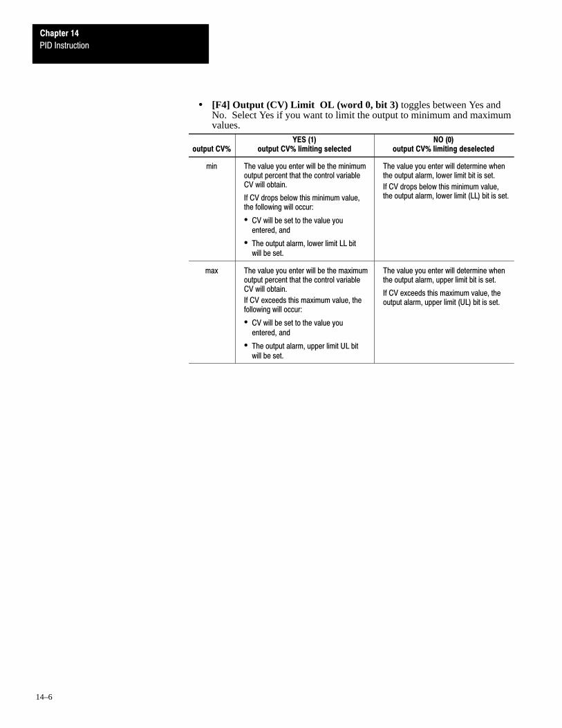
Chapter 14
PID Instruction
14–6
• [F4] Output (CV) Limit OL (word 0, bit 3) toggles between Yes andNo. Select Yes if you want to limit the output to minimum and maximumvalues.
output CV%YES (1)
output CV% limiting selectedNO (0)
output CV% limiting deselected
min The value you enter will be the minimumoutput percent that the control variableCV will obtain.
If CV drops below this minimum value,the following will occur:
• CV will be set to the value youentered, and
• The output alarm, lower limit LL bitwill be set.
The value you enter will determine whenthe output alarm, lower limit bit is set.
If CV drops below this minimum value,the output alarm, lower limit (LL) bit is set.
max The value you enter will be the maximumoutput percent that the control variableCV will obtain.
If CV exceeds this maximum value, thefollowing will occur:
• CV will be set to the value youentered, and
• The output alarm, upper limit UL bitwill be set.
The value you enter will determine whenthe output alarm, upper limit bit is set.
If CV exceeds this maximum value, theoutput alarm, upper limit (UL) bit is set.

Chapter 14
PID Instruction
14–7
Monitor Display Screen
The APS display below shows typical values entered for the variousparameters in the left column. The right column of the display shows thestatus of the PID instruction flags. This is discussed in the following section.An asterisk (∗) denotes that you can not cursor to the field.
F1 auto/manual: AUTO ∗ time mode Bit: 1 TMmode: STI ∗ auto/manual bit: 0 AM
control: E=SP–PV ∗ control mode bit: 0 CMsetpoint (SP): 500 output limiting enabled bit: 1 OL
process (PV): 0 ∗ reset and gain range: 0 RGscaled error: 0 scale setpoint flag: 0 SC
deadband: 5 loop update time too fast: 0 TFoutput (CV): 0 % ∗ derivitive (rate) action: 0 DA
DB, set when error is in DB: 0 DBloop update: 50 [.01 secs] output alarm, upper limit: 0 UL
gain: 25 [/10] output alarm, lower limit: 0 LLreset: 10 [/10 m/r] setpoint out of range: 0 SP
rate: 1 [/100 min] process var out of range: 0 PVmin scaled: 0 ∗ PID done: 0 DNmax scaled: 1000 ∗
F4 output (CV) limit: NO PID enabled: 0 ENoutput (CV) min: 0 %output (CV) max: 0 %
Enter value or press <ESC> to exitN10:4 =offline no forces INSTR INSERT File PIDS
Message:Prompt:Data/Cmd Entry:Status:
Main Functions:
Display Area:
F1 F4
TOGGLEAUTO/MN
TOGGLEOUT LIM
F8
SAVE& EXIT
The right column of the APS display shows various flags associated with thePID instruction. The following section describes those flags:
• Time Mode Bit TM (word 0, bit 0) specifies the PID mode. It is setwhen the TIMED mode is in effect. It is cleared when the STI mode is ineffect. This bit can be set or cleared by instructions in your ladderprogram.
• Auto/Manual Bit AM (word 0, bit 01) specifies automatic operationwhen it is cleared and manual operation when it is set. This bit can be setor cleared by instructions in your ladder program.
• Control Mode Bit CM (word 0, bit 02) is cleared if the control isE=SP–PV. It is set if the control is E=PV–SP. This bit can be set orcleared by instructions in your ladder program.
• Output Limiting Enabled Bit OL (word 0, bit 03) is set when you haveselected to limit the control variable using function key [F4]. This bit canbe set or cleared by instructions in your ladder program.
PID Instruction Flags
Chapter 14
PID Instruction
14–8
• 5/03 specific – Reset and Gain Range Enhancement Bit RG (word 0,bit 4) When set, this bit causes the Reset Minute/Repeat value and thegain multiplier to be enhanced by a factor of 10, (reset multiplier of .01and gain multiplier of .01).For example: The Reset value of 1 indicates that the Integral value of0.01 minutes/repeat (0.6 seconds/repeat) will be applied to the PIDIntegral algorithm. The gain value of 1 indicates that the error will bemultiplied by 0.01 and applied to the PID Proportional algorithm.
When clear, this bit allows the Reset Minutes/Repeat value and the Gainmultiplier value to be evaluated in the same units as the 5/02 PIDinstruction, (reset multiplier of 0.1 and gain multiplier of 0.1).For example: The Reset value of 1 indicates that the Integral value of 0.1minutes/repeat (0.6 seconds/repeat) will be applied to the PID Integralalgorithm. The gain value of 1 indicates that the error will be multipliedby 0.1 and applied to the PID Proportional algorithm.
Note that the Rate multiplier is not affected by this selection. (The initialrelease software, version 4.0, may not allow you to enter this bit.However, you may alter the state of this bit directly in the control block.)
• Scale Setpoint Flag SC (word 0, bit 05) is cleared when setpoint scalingvalues are specified.
• Loop Update Time Too Fast TF (word 0, bit 06) is set by the PIDalgorithm if the loop update time you have specified cannot be achievedby the given program (because of scan time limitations).If this bit is set, try to correct the problem by updating your PID loop at aslower rate or move the PID instruction to an STI interrupt routine. Resetand rate gains will be in error if the instruction operates with this bit set.
• 5/03 specific – Derivitive (Rate) Action Bit DA (word 0, bit 07) Whenset, this bit causes the Derivitive (Rate) calculation to be evaluated on theError instead of the PV. When clear, this bit allows the Derivitive (Rate)calculation to be evaluated the same as the 5/02 PID instruction, (wherederivitive is performed on the PV). (The initial release software, version4.0, may not allow you to enter this bit. However, you may alter the stateof this bit directly in the control block.)
• DB, Set When Error is in DB (word 0, bit 08) is set when the processvariable is within the 0 crossing deadband range.
• Output Alarm, Upper Limit UL (word 0, bit 09) is set when the calculated control output CV exceeds the upper CV limit.
• Output Alarm, Lower Limit LL (word 0, bit 10) is set when thecalculated control output CV is less than the lower CV limit.
• Setpoint Out of Range SP (word 0, bit 11) is set when the setpointexceeds the maximum scaled value or is less than the minimum scaledvalue.
• Process Var Out of Range PV (word 0, bit 12) is set when the unscaled(or raw) process variable exceeds 16383 or is less than zero.
• PID Done DN (word 0, bit 13) is set on scans where the PID algorithm iscomputed. It is computed at the loop update rate.
• PID Enabled EN (word 0, bit 15) is set while the rung of the PIDinstruction is enabled.

Chapter 14
PID Instruction
14–9
The control block length is fixed at 23 words and should be programmed asan integer file. PID instruction flags (word 0) and other parameters arelocated as follows:
EN DN PV SP LL UL DB DA TF SC RG OL CM AM TM
15 14 13 12 11 10 09 08 07 06 05 04 03 02 01 00
PID Sub Error Code (MSbyte)
Setpoint SP
Control Block Layout
Word
0
1
2
Gain K C
Reset T i
Rate T d
3
4
5
6
*
*
*
*
*
7
8
9
10
11
12
Setpoint Max (Smax)
Setpoint Min (Smin)
Deadband
INTERNAL USE DO NOT CHANGE
Output Max
Output Min
*
*
*
*
*
13
14
15
16
Loop Update
Scaled Process Variable
Scaled Error SE
Output CV% (0–100%)
*
17
18
19
20
21
22
INTERNAL USEDO NOT CHANGE
➀ You may alter the state of these values with your ladder program.
OL, CM,AM, TM ➀
Feed Forward Bias*
LSW Integral Sum 5/03 MSW Integral Sum
MSW Integral Sum 5/03 LSW Integral Sum
➁➁
➁ Applies to the 5/03 processor only.
!ATTENTION: Do not alter the state of any PID control blockvalue unless you fully understand its function and related effecton your process.
Control Block Layout

Chapter 14
PID Instruction
14–10
Error code 0036 appears in the status file when a PID instruction runtimeerror occurs. Code 0036 covers the following PID error conditions, each ofwhich has been assigned a unique single byte code value that appears in theMSbyte of the second word of the control block.
Error Code Description of Error Condition or Conditions Corrective Action
11H 5/02 specific 5/03 specific
1) Loop update time Dt > 255, or 1) Loop update time Dt > 1024
2) Loop update time Dt = 0 2) Loop update time Dt = 0
Change loop update time Dt to
0 < Dt < 255
12H 5/02 specific 5/03 specific1) Proportional gain Kc > 255, or 1) Proportional gain Kc < 0
2) Proportional gain Kc = 0
Change proportional gain Kc to
0 < Kc < 255
13H 5/02 specific - Integral gain (reset) Ti > 255
5/03 specific - Integral gain (reset) Ti < 0
Change integral gain (rate) Ti to
0 < Ti < 255
14H 5/02 specific - Derivative gain (rate) Td > 255
5/03 specific - Derivative gain (rate) Td < 0
Change derivative gain (rate) Td to
0 < Td < 255
21H(5/02 only)
1) Scaled setpoint max Smax > 16383, or
2) Scaled setpoint max Smax < -16383
Change scaled setpoint max Smax to
-16383 < Smax < 16383
22H(5/02 only)
1) Scaled setpoint min Smin > 16383, or
2) Scaled setpoint min Smin < -16383
Change scaled setpoint min Smin to
-16383 < Smin < Smax < 16383
23H Scaled setpoint min Smin > Scaled setpoint max Smax Change scaled setpoint min Smin to
-16383 < Smin < Smax < 16383
(5/03 specific: -32768 to +32767)
31H If you are using setpoint scaling and Smin >
setpoint SP > Smax, or
If you are not using setpoint scaling and 0 >
setpoint SP > 16383,
then during the initial execution of the PID loop, this error occurs and
bit 11 of word 0 of the control block is set. However, during subsequent
execution of the PID loop if an invalid loop setpoint is entered, the PID
loop continues to execute using the old setpoint, and bit 11 of word 0
of the control block is set.
If you are using setpoint scaling, then change the
setpoint SP to Smin < SP < Smax, or
If you are not using setpoint scaling, then change
the setpoint SP to 0 < SP < 16383.
41H Scaling Selected Scaling Deselected
1) Deadband < 0, or 1) Deadband < 0, or2) Deadband > 2) Deadband > 16383 (Smax � Smin), or3) Deadband > 16383
(5/02 specific)
Scaling Selected Scaling Deselected
Change deadband to Change deadband to0 < deadband < 0 < deadband <(Smax - Smin) < 1638316383
51H 1) Output high limit < 0, or
2) Output high limit > 100
Change output high limit to
0 < output high limit < 100
52H 1) Output low limit < 0, or
2) Output low limit > 100
Change output low limit to
0 < output low limit < output high limit < 100
53H Output low limit > output high limit Change output low limit to
0 < output low limit < output high limit < 100
60H 5/02 specific - PID is being entered for the second time. (PID loop was
interrupted by an I/O interrupt, which is then interrupted by the PID
STI interrupt.)
You have at least three PID loops in your program: One in the main
program or subroutine file, one in an I/O interrupt file, and one in the STI
subroutine file. You must alter your ladder program and eliminate the
potential nesting of PID loops.
Runtime Errors

Chapter 14
PID Instruction
14–11
For the SLC 500 PID instruction, the numerical scale for both the processvariable (PV) and the control variable (CV) is 0 to 16383. To useengineering units, such as PSI or degrees, you must first scale your analogI/O ranges within the above numerical scale. To do this, use the Scale (SCL)instruction and follow the steps described below. Refer to the Analog I/OModules User Manual, Catalog Number 1746–NM003 for more information.
Scale your analog input by calculating the slope (or rate) of the analog inputrange to the PV range (0 to 16383.) For example, an analog input with arange of 4 to 20mA has a decimal range of 3277 to 16384. The decimalrange must be scaled across the range of 0 to 16383 for use as PV.
Scale the CV to span evenly across your analog output range. For example,an analog output which is scaled at 4 to 20mA has a decimal range of 6242 to31208. In this case, 0 to 16383 must be scaled across the range of 6242 to31208.
Once you have scaled your analog I/O ranges to/from the PID instruction,you can enter the minimum and maximum engineering units that apply toyour application. For example, if the 4 to 20mA analog input rangerepresents 0 to 300 PSI, you can enter 0 and 300 as the minimum (Smin) andmaximum (Smax) parameters respectively. The Process Variable, Error,Setpoint, and Deadband will be displayed in engineering units in the PIDData Monitor screen. Setpoint and Deadband can be entered into the PIDinstruction using engineering units.
The following equations show the linear relationship between the input valueand the resulting scaled value.
Scaled value = (input value x slope) + offset
Slope = (scaled max. − scaled min.) / (input max. − input min)
Offset = scaled min. − (input min. x slope)
Use the following values in an SCL instruction to scale common analog inputranges to PID process variables.
Parameter 4 to 20mA 0 to 5V 0 to 10V
Rate/10,000 12,499 10,000 5,000
Offset -4096 0 0
Use the following values in an SCL instruction to scale control variables tocommon analog outputs.
Parameter 4 to 20mA 0 to 5V 0 to 10V
Rate/10,000 15,239 10,000 19,999
Offset 6242 0 0
PID and Analog I/O Scaling

Chapter 14
PID Instruction
14–12
The following ladder diagram shows a typical PID loop that is programmedin the STI mode. This example is provided primarily to show the properscaling techniques. It shows a 4 to 20mA analog input and a 4 to 20mAanalog output.
SCLSCALESource I:1.0
0Rate [/10000] 12499
Offset –4096
Dest N10:280
LESLESS THANSource A I:1.0
0Source B 3277
GRTGREATER THANSource A I:1.0
0Source B 16384
MOVMOVESource 3277
Dest I:1.00
IIMIMMEDIATE IN w MASKSlot I:1.0Mask FFFF
(L)B3
0
This rung immediately updates the analog input used for PV.
Rung 3:0
Rung 3:1
Rung 3:2
Rung 3:3
Rung 3:4
These two rungs ensure the analog input value to be scaled remains within the limits of 3277 to 16384. This is necessary toprevent �out of range" conversion errors in both the SCL and PID instructions. The latch bits can be used elsewhere in yourprogram to identify the particular out of range condition that occurred.
Under range
MOVMOVESource 16384
Dest I:1.00
(L)B3
1
Over range
The source to be scaled is the input I:1 and its destination is the process variable of the PID instruction. These values arecalculated knowing that the input range is 3277 to 16384, while the scaled range (PV) is 0 to 16383.
PIDPIDControl Block N10:0Process Variable N10:28Control Variable N10:29Control Block Length 23

Chapter 14
PID Instruction
14–13
IOMIMMEDIATE OUT w MASKSlot O:1.0Mask FFFF
END
Rung 3:6
Rung 3:5
SCLSCALESource N10:29
0Rate [/10000] 15239
Offset 6242
Dest O:1.00
The PID control variable is the input for the scale instruction. The PID instruction guarantees that the CV remains withinthe range of 0 to 16383. This value is to be scaled to the range of 6242 to 31208, which represents the numeric rangethat is needed to produce 4 to 20mA analog output signal.
This rung immediately updates the analog output card that is driven by the PID control variable value.

Chapter 14
PID Instruction
14–14
The following paragraphs discuss:
• Input/Output Ranges• Scaling to Engineering Units• Zero-crossing Deadband• Output Alarms• Output Limiting with Anti-reset Windup• The Manual Mode• Feed Forward• Time Proportioning Outputs
Input/Output Ranges
The input module measuring the process variable (PV) must have a full scalebinary range of 0 to 16383. If this value is less than 0 (bit 15 set), then avalue of zero will be used for PV and the “Process var out of range” bit willbe set (bit 12 of word 0 in the control block). If the process variable is >16383 (bit 14 set), then a value of 16383 will be used for PV and the“Process var out of range” bit will be set.
The Control Variable, calculated by the PID instruction, has the same rangeof 0 to 16383. The Control Output (word 16 of the control block) has therange of 0 to 100%. You can set lower and upper limits for the instruction’scalculated output values (where an upper limit of 100% corresponds to aControl Variable limit of 16383).
Scaling to Engineering Units
Scaling lets you enter the setpoint and zero-crossing deadband values inengineering units, and to display the process variable and error values in thesame engineering units. Remember, the process variable PV must still bewithin the range 0–16383. The PV will be displayed in engineering units,however.
Select scaling as follows:
1. Enter the maximum and minimum scaling values Smax and Smin in thePID control block. Refer to the control block of the PID instruction onpage 14–9. The Smin value corresponds to an analog value of zero forthe lowest reading of the process variable, and Smax corresponds to ananalog value of 16383 for the highest reading. These values reflect theprocess limits. Setpoint scaling is selected by entering a non-zero valuefor one or both parameters. If you enter the same value for bothparameters, setpoint scaling is disabled.
Application Notes

Chapter 14
PID Instruction
14–15
For example, if measuring a full scale temperature range of – 73 (PV=0) to+1156° C (PV=16383), enter a value of –73 for Smin and 1156 for Smax.Remember that inputs to the PID instruction must be 0 to 16383. Signalconversions could be as follows:
Process limits −73 to +1156° C
Transmitter output (if used) +4 to +20 mA
Output of analog input module 0 to 16383mA
PID instruction, Smin to Smax −73 to +1156° C
2. Enter the setpoint (word 2) and deadband (word 9) in the same scaledengineering units. Read the scaled process variable and scaled error inthese units as well. The control output percentage (word 16) is displayedas a percentage of the 0 to 16383 CV range. The actual value transferredto the CV output is always between 0 and 16383.
When you select scaling, the instruction scales the setpoint, deadband,process variable, and error. You must consider the effect on all thesevariables when you change scaling.
Zero-crossing Deadband DB
The adjustable deadband lets you select an error range above and below thesetpoint where the output does not change as long as the error remains withinthis range. This lets you control how closely the process variable matchesthe setpoint without changing the output.
+DB
SP
-DB
Error range
Time
Zero-crossing is deadband control that lets the instruction use the error forcomputational purposes as the process variable crosses into the deadbanduntil it crosses the setpoint. Once it crosses the setpoint (error crosses zeroand changes sign) and as long as it remains in the deadband, the instructionconsiders the error value zero for computational purposes.
Select deadband by entering a value in the deadband storage word (word 9)in the control block. The deadband extends above and below the setpoint bythe value you enter. A value of zero inhibits this feature. The deadband hasthe same scaled units as the setpoint if you choose scaling.

Chapter 14
PID Instruction
14–16
Output Alarms
You may set an output alarm on the control output (CO) at a selected valueabove and/or below a selected output percent. When the instruction detectsthat the output (CO) has exceeded either value, it sets an alarm bit (bit 10 forlower limit, bit 9 for upper limit) in word 0 of the PID control block. Alarmbits are reset by the instruction when the output (CO) comes back inside thelimits. The instruction does not prevent the output (CO) from exceeding thealarm values unless you select output limiting.
Select upper and lower output alarms by entering a value for the upper alarm(word 11) and lower alarm (word 12). Alarm values are specified as apercentage of the output. If you do not want alarms, enter zero and 100%respectively for lower and upper alarm values and ignore the alarm bits.
Output Limiting with Anti�reset Windup
You may set an output limit (percent of output) on the control output. Whenthe instruction detects that the output (CO) has exceeded a limit, it sets analarm bit (bit 10 for lower limit, bit 9 for upper limit) in word 0 of the PIDcontrol block, and prevents the output (CO) from exceeding either limitvalue. The instruction limits the output (CO) to 0 and 100% if you choosenot to limit.
Select upper and lower output limits by setting the limit enable bit (bit 3 ofcontrol word 0), and entering an upper limit (word 11) and lower limit (word12). Limit values are a percentage (0 to 100%) of the control output (CO).
The difference between selecting output alarms and output limits is that youmust select output limiting to enable limiting. Limit and alarm values arestored in the same words. Entering these values enables the alarms, but notlimiting. Entering these values and setting the limit enable bit enableslimiting and alarms.
Anti-reset windup is a feature that prevents the integral term from becomingexcessive when the output (CO) reaches a limit. When the sum of the PIDand bias terms in the output (CO) reaches the limit, the instruction stopscalculating the integral sum until the output (CO) comes back in range. Theintegral sum is contained in Words 17 and 18 of the control block.
Chapter 14
PID Instruction
14–17
The Manual Mode
In the manual mode, the PID algorithm does not compute the value of thecontrol variable. Rather, it uses the value as an input to adjust the integralsum (words 17 and 18) so that a bumpless transfer takes place uponre-entering the AUTO mode.
In the manual mode, the programmer allows you to enter a new CV valuefrom 0 to 100%. This value is converted into a number from 0 to 16383 andwritten to the Control Variable address. If you are using an analog outputmodule for this address, you must save (compile) the program with the FileProtection option set to None. This allows writing to the output data table.If you do not perform this save operation, you will not be able to set theoutput level in the manual mode. If your ladder program sets the manualoutput level, design your ladder program to write to the CV address when inthe manual mode. Note that this number is in the range of 0 to 16383, not 0to 100. Writing to the CV percent (word 16) with your ladder program hasno effect in the manual mode.
The example on the next page shows how you can manually control thecontrol variable (CV) output with your ladder program.
PID Rungstate
If the PID rung is false, the integral sum (words 17 and 18) is cleared and CVremains in its last state.

Chapter 14
PID Instruction
14–18
Notes on Operation
A 3�digit BCD thumbwheel is wired to an inputmodule at I1:1.0 (range 0-100).
A pushbutton wired to I1:2.0/0 accepts thethumbwheel value.
A selector switch for auto/manual mode is wiredto I1:2.0/1 (auto) and I1:2.0/2 (manual).
N7:0 stores the value entered on thethumbwheel switch.
N7:2 stores an intermediate calculation.
N7:8 is the PID control variable address.
N7:10 is the control block address of the PIDinstruction.
N7:26 Percent output is updated automaticallyby the PID instruction.
] [N7:10
1[OSR]
B3
0
( )B3
3
MULMULTIPLYSource A N7:0
Source B 16384
Dest N7:2
LIMLIMIT TESTLow Lim 0
Test N7:0
High Lim 100
FRDFROM BCDSource I1:1.0
Dest N7:0
DDVDOUBLE DIVIDESource 100
Dest N7:8
] [I:2.0
0
(U)S:5
0
] [I:2.0
1
Accept CV
Error - Out of Range
Auto
] [I:2.0
2
Manual
(L)N7:10
1
(U)N7:10
1
A/M Bit
A/M Bit
A/M Bit
LIMLIMIT TESTLow Lim 101
Test N7:0
High Lim –1
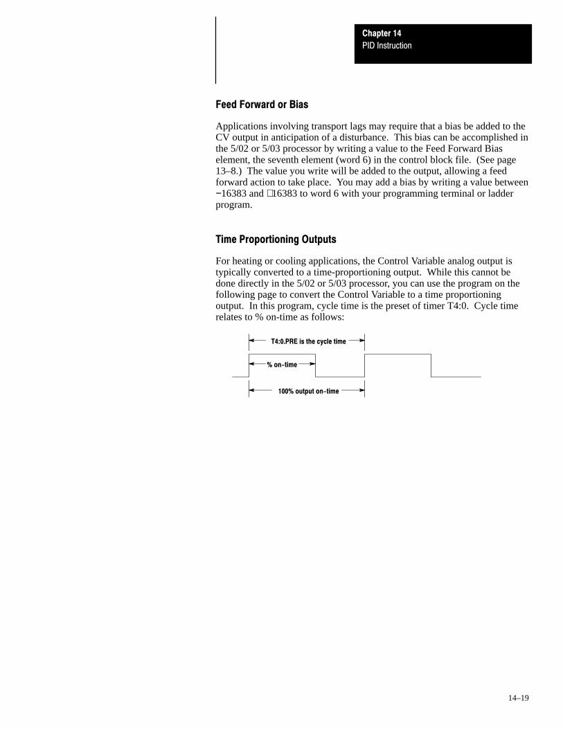
Chapter 14
PID Instruction
14–19
Feed Forward or Bias
Applications involving transport lags may require that a bias be added to theCV output in anticipation of a disturbance. This bias can be accomplished inthe 5/02 or 5/03 processor by writing a value to the Feed Forward Biaselement, the seventh element (word 6) in the control block file. (See page13–8.) The value you write will be added to the output, allowing a feedforward action to take place. You may add a bias by writing a value between−16383 and +16383 to word 6 with your programming terminal or ladderprogram.
Time Proportioning Outputs
For heating or cooling applications, the Control Variable analog output istypically converted to a time-proportioning output. While this cannot bedone directly in the 5/02 or 5/03 processor, you can use the program on thefollowing page to convert the Control Variable to a time proportioningoutput. In this program, cycle time is the preset of timer T4:0. Cycle timerelates to % on-time as follows:
T4:0.PRE is the cycle time
100% output on-time
% on-time
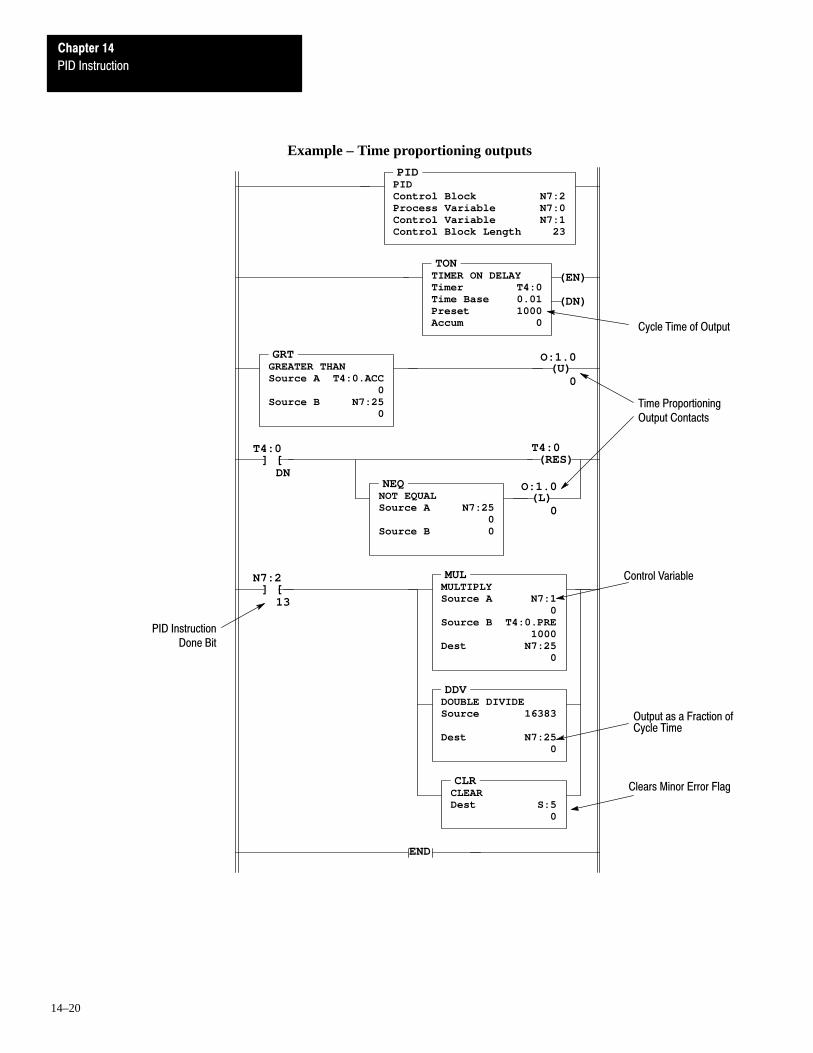
Chapter 14
PID Instruction
14–20
Example – Time proportioning outputs
(L)O:1.0
0
(U)O:1.0
0
(RES)T4:0
(EN)
(DN)
TONTIMER ON DELAYTimer T4:0Time Base 0.01Preset 1000Accum 0
NEQNOT EQUALSource A N7:25
0Source B 0
GRTGREATER THANSource A T4:0.ACC
0Source B N7:25
0
MULMULTIPLYSource A N7:1
0Source B T4:0.PRE
1000Dest N7:25
0
DDVDOUBLE DIVIDESource 16383
Dest N7:250
CLRCLEARDest S:5
0
PIDPIDControl Block N7:2Process Variable N7:0Control Variable N7:1Control Block Length 23
END
] [T4:0
DN
] [N7:2
13
Cycle Time of Output
Time Proportioning
Control Variable
Clears Minor Error Flag
PID Instruction
Output Contacts
Done Bit
Output as a Fraction ofCycle Time
Chapter 14
PID Instruction
14–21
PID Tuning
PID tuning requires a knowledge of process control. If you areinexperienced, it will be helpful if you obtain training on the process controltheory and methods used by your company.
There are a number of techniques that can be used to tune a PID loop. Thefollowing PID tuning method is general, and is limited in terms of handlingload disturbances. When tuning, we recommend that changes be made in theMANUAL mode, followed by a return to AUTO. Output limiting is appliedin the MANUAL mode.
Important: This method requires that the PID instruction controls anon-critical application in terms of personal safety andequipment damage.
Procedure
1. Create your ladder program. Make certain that you have properly scaledyour analog input to the range of the process variable PV and that youhave properly scaled your control variable CV to your analog output.
2. Connect your process control equipment to your analog modules.Download your program to the processor. Leave the processor in theprogram mode.
!ATTENTION: Ensure that all possibilities of machine motionhave been considered with respect to personal safety andequipment damage. It is possible that your output CV may swingbetween 0 and 100% while tuning.
If you want to verify the scaling of your continuous system and/ordetermine the initial loop update time of your system, go to theprocedure on page 14–23.
3. Enter the following values: The initial setpoint SP value, a reset Ti of 0, arate Td of 0, a gain Kc of 1, and a loop update of 5.Set the PID mode to STI or Timed, per your ladder diagram. If STI isselected, ensure that the loop update time equals the STI time interval.
Enter the optional settings that apply (output limiting, output alarm,Smax – Smin scaling, feedforward).
4. Get prepared to chart the CV, PV, analog input, or analog output as itvaries with time with respect to the setpoint SP value.
5. Place the PID instruction in the MANUAL mode, then place theprocessor in the Run mode.
6. While monitoring the PID display, adjust the process manually by writingto the CO percent value.
7. When you feel that you have the process under control manually, placethe PID instruction in the AUTO mode.

Chapter 14
PID Instruction
14–22
8. Adjust the gain while observing the relationship of the output to thesetpoint over time.
When using the 5/02 processor, gain adjustments disrupt the process whenyou change values. To avoid this disruption, switch to the MANUALmode prior to making your gain change, then switch back to the AUTOmode. When using the 5/03 processor, gain changes do not disrupt theprocess, therefore you do not need to switch to the MANUAL mode.
9. When you notice that the process is oscillating above and below thesetpoint in an even manner, record the time of 1 cycle. That is, obtain thenatural period of the process.Natural Period ≅ 4x deadtime
Record the gain value. Return to the MANUAL mode (stop the process ifnecessary).
10. Set the loop update time (and STI time interval if applicable) to a value of5 to 10 times faster than the natural period.If the cycle time is 20 seconds for example, and you choose to set theloop update time to 10 times faster than the natural rate, set the loopupdate time to 200, which would result in a 2-second rate.
11. Set the gain Kc value to 1/2 the gain needed to obtain the natural period ofthe process. For example, if the gain value recorded in step 9 was 80, setthe gain to 40.
12. Set the reset term Ti to approximate the natural period. If the naturalperiod is 20 seconds, as in our example, you would set the reset term to 3(0.3 minutes per repeat approximates 20 seconds).
13. Now set the rate Td equal to a value 1/8 that of the reset term. For ourexample, the value 4 will be used to provide a rate term of 0.04 minutesper repeat.
14. Place the process in the AUTO mode. If you have an ideal process, thePID tuning will be complete.
15. To make adjustments from this point, place the PID instruction in theMANUAL mode, enter the adjustment, then place the PID instructionback in the AUTO mode.This technique of going to MANUAL, then back to AUTO ensures thatmost of the “gain error” is removed at the time each adjustment is made.This allows you to see the effects of each adjustment immediately.Toggling the PID rung allows the PID instruction to restart itself,eliminating all of the “integral buildup.” You may want to toggle the PIDrung false while tuning to eliminate the effects of previous tuningadjustments.

Chapter 14
PID Instruction
14–23
Verifying the Scaling of Your Continuous System
To ensure that your process is linear, and that your equipment is properlyconnected and scaled, do the following:
1. Place the PID instruction in manual and enter the following parameters:
• type: 0 for Smin• type: 100 for Smax• type: 0 for CO%
2. Enter the REM Run mode and verify that PV=0.
3. Type: 20 in CO%
4. Record the PV = _______
5. Type: 40 in CO%.
6. Record the PV = _______
7. Type: 60 in CO%.
8. Record the PV = _______
9. Type: 80 in CO%.
10. Record the PV = _______
11. The values you recorded should be offset from CO% by the same amount.This proves the linearity of your process. The following example showsan offset progression of fifteen.
CO 20% = PV 35%CO 40% = PV 55%CO 60% = PV 75%CO 80% = PV 95%
If the values you recorded are not offset by the same amount:
• Either your scaling is incorrect, or• the process is not linear, or• your equipment is not properly connected and/or configured.
Make the necessary corrections and repeat steps 2–10.
Determining the Initial Loop Update Time
To determine the approximate loop update time that should be used for yourprocess, perform the following:
1. Place the normal application values in Smin and Smax.
2. Type: 50 in CO%.
3. Type: 60 in CO% and immediately start your stopwatch.
4. Watch the PV. When the PV starts to change, stop your stopwatch.Record this value. It is the deadtime.
Chapter 14
PID Instruction
14–24
5. Multiply the deadtime by 4. This value approximates the natural period.For example, if:deadtime = 3 seconds, then 4 � 3 = 12 seconds (≅ natural period)
6. Divide the value obtained in step 5 by 10. Use this value as the loopupdated time. For example, if:natural period = 12 seconds, then 12 � 10 = 1.2 seconds.Therefore, the value 120 would be entered as the loop update time.(120 ��10 ms = 1.2 seconds)
7. Enter the following values: The initial setpoint SP value, a reset Ti of 0, arate Td of 0, a gain Kc of 1, and the loop update time determined in step17.
Set the PID mode to STI or Timed, per your ladder diagram. If STI isselected, ensure that the loop update time equals the STI time interval.
Enter the optional settings that apply (output limiting, output alarm,Smax – Smin scaling, feedforward).
8. Return to page 14–21 and complete the tuning procedure starting withstep 4.
15Chapter
15–1
Troubleshooting Faults
This chapter lists the major error fault codes, indicates the probable causes offaults, and recommends corrective action. This chapter also explains theoperating system download faults for the 5/03 processor.
Chapter 1 of this manual also lists the error codes, Word S:6.
Use one of the following methods to clear a processor fault when the faultroutine is not in effect.
Automatically Clearing Faults
The following section describes the different ways to automatically clear afault using APS.
• Set the Fault Override at Powerup Bit S:1/8 in the status file to clear thefault when power is cycled, assuming the user program is not corrupt.
• Set one of the autoload bits S:1/10, S:1/11, or S:1/12 in the status file ofthe program in an EEPROM to automatically transfer a new non-faultedprogram from the memory module to RAM when power is cycled.
Refer to chapter 1 in this manual for more information on status bits S:1/13,S:1/8, S:1/10, S:1/11, S:1/12, S:5/0–7, and S:36/0–7.
Important: You can declare your own application-specific major fault bywriting your own unique value to S:6 and then setting bitS:1/13.
Manually Clearing Faults
The following section describes the different ways to manually clear a fault.
• Manually clear the major fault bit S:1/13, and the minor and major errorbits S:5/0–7 in the status file, using a programming device or a Data TableAccess Module. Place the processor in the REM Program mode. Correctthe condition causing the fault, then return the processor to either REMRun or any of the REM Test modes.
• 5/03 specific – Toggle the keyswitch from RUN to PROGram and thenback to RUN.
!ATTENTION: 5/03 specific – Clearing these bits with thekeyswitch in the RUN position causes the processor toimmediately enter the Run mode.
Clearing Faults

Chapter 15
Troubleshooting Faults
15–2
To remove a fault condition and return to the RUN or REM Run mode usingAPS, do the following:
1. Press CONFIGOFFLINE
CONFIGONLINE
F1
, then CONFIGOFFLINE
CONFIGDATA
MONITOR
F9
. Press the letter S and then press
[ ENTER] . The first screen of the status file contains the fault code andfault description.
2. Remove the fault by pressing CONFIGOFFLINE
CONFIGCLR MAJ
FAULT
F10
. This clears words S:1/13, S:5,
and S:6.
3. Once the fault code is cleared, the code 0000 is displayed.
4. Re-enter the RUN or REM Run mode. When you return to the Run modeall forces and latches are in effect.
!ATTENTION: If you are online with a 5/03 processor and thekeyswitch position is in RUN and you press the clear major faultfunction key, you are warned that the processor will enter the Runmode once you clear the fault.
User Fault Routine in Effect - 5/02 and 5/03 Processors Only
When designating a subroutine file, the occurrence of recoverable ornon-recoverable user faults causes the designated subroutine to be executedfor one scan. If the fault is recoverable, the subroutine can be used to correctthe problem and clear the fault bit S:1/13. The processor then continues inthe run mode. If the fault is non-recoverable, the subroutine can send amessage via the Message instruction to another DH–485 node with errorcode information and/or does an orderly shutdown of the process.
The subroutine does not execute for non-user faults. The user fault routine isdiscussed in chapter 16.

Chapter 15
Troubleshooting Faults
15–3
The status file display is accessible offline and online from the Data Monitoror General Utility function. It shows:A– Word S:1. Bit S:1/13 in this word is the major fault bit. Cleared bypressing [F10].
B –Word S:5. Minor fault bits. Cleared by pressing [F9].
C– Word S:6. Fault code. Cleared by pressing [F10].
D –Fault description. A textual description of the fault code. Cleared bypressing [F10].
D
C
B
Press function key or enter value, press Alt–H for help.S:0/0 = offline no forces formatted decimal addr File 09TEST
Message:Prompt:Data/Cmd Entry:Status:
Main Functions:
F7F5
NEXTFILE
SPECIFYADDRESS
ARITHMETIC FLAGS S:0 Z:0 V:0 C:0
PROCESSOR STATUS 00000000 00000000 SUSPEND CODE 0PROCESSOR STATUS 00000000 00000001 SUSPEND FILE 0PROCESSOR STATUS 00000000 00000000 WATCHDOG [x10 ms] 10MINOR FAULT 00000000 00000000 LAST SCAN [x10 ms] 0FAULT CODE 0000 FREE RUNNING CLOCK 00000000 00000000FAULT DESCRIPTION:
MATH REGISTER 0000 0000
ACTIVE NODE LIST I/O SLOT ENABLES0 10 20 30 0 10 20 3011000000 00000000 00000000 00000000 11111111 11111111 11111111 11111111
PROCESSOR BAUD RATE (Channel 1) 19200 PROCESSOR ADDRESS: 1
F9 F10F8
CLR MINFAULT
CLR MAJFAULT
PREVFILE
A
F1
PAGEUP
F2
PAGEDOWN
Status File Fault Display

Chapter 15
Troubleshooting Faults
15–4
Between the time you apply power to the 5/03 processor and it has a chanceto establish communication with a connected programming device, the onlyform of communication between you and the 5/03 processor is through theLED display.
Powerup LED Display
When power is applied, all of the LEDs flash on momentarily and then off.This is part of the normal powerup sequence. Following the selftest by theprocessor, all of the LEDs will flash on again momentarily. If a userprogram is in a running state the RUN LED will be illuminated. If a faultexists within the processor, the FLT LED will be illuminated.
LED Display While Downloading an Operating System
The download process takes approximately 45 seconds. During this time,watch the LED display for status information. While the download is inprogress, the RUN and FLT LEDs remain off. The RS232, DH485, FORCE,and BATT LEDs illuminate in a pre–defined sequence. If the download issuccessful, the above LEDs will be illuminated.
If during the download process of an operating system type memory moduleor during the normal powerup selftest process an error occurs, the FLT LEDwill be illuminated and the four LEDs will flash on and off at a rate of 2seconds.
The following table describes the possible LED combinations that will bedisplayed every other time the LEDs flash on.
ON LED Display Description
FAULT, FORCE, DH485 Fatal hardware error exists.
FAULT, FORCE, RS232, DH485 A hardware watchdog timeout exists.
FAULT, BATT NVRAM error exists.
FAULT, BATT, RS232The contents of the operating system memorymodule are corrupt.
FAULT, BATT, DH485The downloadable operating system is notcompatible with the hardware.
FAULT, BATT, RS232, DH485An attempt was made to download the operatingsystem onto write-protected memory.
FAULT, BATT, FORCE Flash EEPROM failure.
FAULT, BATT, FORCE, RS232Failure during transmission of downloadableoperating system.
FAULT, BATT, FORCE, DH485The operating system is missing or has beencorrupted.
Troubleshooting the 5/03Processor

Chapter 15
Troubleshooting Faults
15–5
The following error types are explained:
• Powerup• Going-to-Run• Runtime• User Program Instruction• I/O
Each table lists the error code description, the probable cause, and therecommended corrective action.
Powerup Errors
Error Code (Hex)
Description Probable Cause Recommended Action
0001 NVRAM error. • Either noise,• lightning,• improper grounding,• lack of surge suppression on outputs
with inductive loads, or• poor power source.• Loss of battery or capacitor backup.
Correct the problem, reload the program,and run. You can use the autoload featurewith a memory module to automaticallyreload the program and enter the Runmode.
0002 Unexpected hardware watchdog timeout. • Either noise,• lightning,• improper grounding,• lack of surge suppression on outputs
with inductive loads, or• poor power source.
Correct the problem, reload the program,and run. You can use the autoload featurewith a memory module to automaticallyreload the program and enter the Runmode.
0003 Memory module memory error. This errorcan also occur when going to the REMRun mode.
Memory module is corrupted. Re�program the memory module. If theerror persists, replace the memory module.
0007 Failure during memory module transfer. Memory module is corrupted. Re-program the memory module. If theerror persists, replace the memory module.
0008 Internal software error. An unexpected software error occurreddue to:• Either noise,• lightning,• improper grounding,• lack of surge suppression on output with inductive loads, or• poor power source.
Correct the problem, reload the program,and run. You can use the autoload featurewith a memory module to automaticallyreload the program and enter the Runmode.If the problem re-occurs, contact your A-Brepresentative.
0009 Internal hardware error. An unexpected hardware error occurreddue to:• Either noise,• lightning• improper grounding,• lack of surge suppression on output with inductive loads, or• poor power source.
Correct the problem, reload the program,and run. You can use the autoload featurewith a memory module to automaticallyreload the program and enter the Runmode.If the problem re-occurs, contact your A-Brepresentative.
Error Code Description,Cause, and RecommendedAction

Chapter 15
Troubleshooting Faults
15–6
Going-to-Run Errors
Error Code (Hex)
Description Probable Cause Recommended Action
0010 The processor does not meet the requiredrevision level.
The revision level of the processor is notcompatible with the revision level for whichthe program was developed.
Consult your local A�B representative topurchase an upgrade kit for yourprocessor.
0011 The executable program file number 2 isabsent.
Incompatible or corrupt program is present. Reload the program or reprogram with A�Bapproved APS programming software.
0012 The ladder program has a memory error. • Either noise,• lightning,• improper grounding,• lack of surge suppression on outputs
with inductive loads, or• poor power source.
Correct the problem, reload the program,and run. If the error persists, be sure touse A�B approved APS programmingsoftware to develop and load the program.
0013 • The required memory module isabsent, or
• S:1/10 or S:1/11 is not set as requiredby the program.
• Either one of the status bits is set in theprogram but the required memorymodule is absent, or
• status bit S:1/10 or S:1/11 is not set inthe program stored in the memorymodule, but it is set in the program inthe processor memory.
• Either install a memory module in theprocessor, or
• upload the program from the processorto the memory module.
0014 Internal file error. • Either noise,• lightning,• improper grounding,• lack of surge suppression on outputs
with inductive loads, or• poor power source.
Correct the problem, reload the program,and run. If the error persists, be sure touse A�B approved APS programmingsoftware to develop and load the program.
0015 Configuration file error. • Either noise,• lightning,• improper grounding,• lack of surge suppression on
outputs with inductive loads, or• poor power source.
Correct the problem, reload the program,and run. If the error persists, be sure touse A�B approved APS programmingsoftware to develop and load the program.
0016 Startup protection after power loss. Errorcondition exists at powerup when bit S:1/9is set and powerdown occurred whilerunning.
Status bit S:1/9 has been set by the userprogram. Refer to chapter 1 for details onthe operation of status bit S:1/9.
• Either reset bit S:1/9 if this is consistentwith the application requirements, andchange the mode back to run, or
• clear S:1/13, the major fault bit, beforethe end of the first program scan isreached.
0017 NVRAM/memory module user programmismatch.
Bit S:2/9 is set and the memory moduleuser program does not match the NVRAMuser program.
Transfer the memory module program toNVRAM then change to Run mode.
0018 Incompatible user program. Operatingsystem type mismatch. This error can alsooccur during powerup.
The user program is too advanced to beexecuted in the current operating system.
Contact your A-B representative forinformation about available operatingsystems for the 5/03 processor.
0019 A duplicate label number was detected. A duplicate or missing label instruction wasfound in a subroutine.
• Either remove the duplicate label, or• add a label.

Chapter 15
Troubleshooting Faults
15–7
Runtime Errors
Error Code (Hex)
Description Probable Cause Recommended Action
001F A program integrity problem occurredduring an online editing session.
Either noise, communication loss, or apower cycle occurred during an online editsession.
Reload the program and re-enter yourchanges.
0004 Memory error occurred while in the Runmode.
• Either noise,• lightning,• improper grounding,• lack of surge suppression on outputs
with inductive loads, or• poor power source.
Correct the problem, reload the program,and run. You can use the autoload featurewith a memory module to automaticallyreload the program and enter the Runmode.
0020 A minor error bit is set at the end of thescan. Refer to S:5 minor error bits.
• Either a math or FRD instructionoverflow has occurred,
• sequencer or shift register instructionerror was detected,
• a major error was detected whileexecuting a user fault routine, or
• M0-M1 file addresses were referencedin the user program for a disabled slot.
Correct the programming problem, reloadthe program and enter the run mode. Seealso minor error bits S:5 in chapter 1.
0021 A remote power failure of an expansion I/Orack has occurred.
Note: A modular system that encountersan over-voltage or over-current conditionin any of its power supplies can produceany of the I/O error codes listed on pages15-10 through 15-12 (instead of code0021). The over-voltage or over-currentcondition is indicated by the power supplyLED being off.
ATTENTION: Fixed and FRN 1through 4 5/01 processors - if theremote power failure occurred whilethe processor was in the REM Runmode, error 0021 will cause themajor error halted bit (S:1/13) to becleared at the next powerup of thelocal rack.
5/02 processor and FRN 5 5/01processors - power to the local rackdoes not need to be cycled toresume the REM Run mode. Oncethe remote rack is re-powered, theCPU will restart the system.
!
Fixed and FRN 1 to 4 5/01 processors:Power was removed or the power dippedbelow specification for an expansion rack.
5/02 processors and FRN 5 5/01processors: This error code is presentonly while power is not applied to anexpansion rack. This is the onlyself�clearing error code. When power isre�applied to the expansion rack, the faultwill be cleared.
Fixed and FRN 1 to 4 5/01 processors:Cycle power on the local rack.
5/02 processors and FRN 5 5/01processors: Re�apply power to theexpansion rack.
0022 The user watchdog scan time has beenexceeded.
• Either Watchdog time is set too low forthe user program, or
• user program caught in a loop.
• Either increase the watchdog timeout inthe status file (S:3H), or
• correct the user program problem.
0023 Invalid or non�existent STI interrupt file. • Either an STI interrupt file number wasassigned in the status file, but thesubroutine file was not created, or
• the STI interrupt file number assignedwas 0, 1, or 2.
• Either disable the STI interrupt setpoint(S:30) and file number (S:31) in thestatus file, or
• create an STI interrupt subroutine filefor the file number assigned in thestatus file (S:31). The file number mustnot be 0, 1, or 2.

Chapter 15
Troubleshooting Faults
15–8
Error Code (Hex)
Description Probable Cause Recommended Action
0024 Invalid STI interrupt interval (greater than2550 ms or negative).
The STI setpoint is out of range (greaterthan 2550 ms or negative).
• Either disable the STI interrupt setpoint(S:30) and file number (S:31) in thestatus file, or
• create an STI interrupt routine for thefile number referenced in the status file(S:31). The file number must not be 0,1, or 2.
0025 Excessive stack depth/JSR calls for theSTI routine.
A JSR instruction is calling for a filenumber assigned to an STI routine.
Correct the user program to meet therequirements and restrictions for the JSRinstruction, then reload the program andrun.
0026 Excessive stack depth/JSR calls for an I/Ointerrupt routine.
A JSR instruction is calling for a filenumber assigned to an I/O interruptroutine.
Correct the user program to meet therequirements and restrictions for the JSRinstruction, then reload the program andrun.
0027 Excessive stack depth/JSR calls for theuser fault routine.
A JSR instruction is calling for a filenumber assigned to the user fault routine.
Correct the user program to meet therequirements and restrictions for the JSRinstruction, then reload the program andrun.
0028 Invalid or non�existent �startup protection"fault routine file value.
• Either a fault routine file number wascreated in the status file, but the faultroutine file was not physically created,or
• the file number created was 0, 1, or 2.
• Either disable the fault routine filenumber (S:29) in the status file, or
• create a fault routine for the file numberreferenced in the status file (S:29). Thefile number must not be 0, 1, or 2.
0029 Indexed address reference is outside ofthe entire data file space (range of B3:0through the last file).
ATTENTION: The 5/02 processoruses an index value of zero for thefaulted instruction following errorrecovery.
!
The program is referencing throughindexed addressing an element beyondthe allowed range. The range is from B3:0to the last element of the last data filecreated by the user.
Correct and reload the user program. Thisproblem cannot be corrected by writing tothe index register word (S:24).
002A Indexed address reference is beyond thespecific referenced data file.
The program is referencing throughindexed addressing an element beyond afile boundary.
Correct the user program, allocate moredata space using the memory map, orre�save the program allowing crossing offile boundaries. Reload the user program.This problem cannot be corrected bywriting to the index register word (S:24).
002E Invalid DII Input slot. The referenced slot is empty or anon-discrete I/O card is present.
Change the input slot to a discrete I/Ocard.
002F Invalid or non�existent DII interrupt file. • Either an DII interrupt file number wasassigned in the status file, but thesubroutine file was not created, or
• the DII interrupt file number assignedwas 0, 1, or 2.
Either disable the DII function by writing azero to this location, or change the value toa valid ladder file (3-255).

Chapter 15
Troubleshooting Faults
15–9
User Program Instruction Errors
Error Code (Hex)
Description Probable Cause Recommended Action
0030 An attempt was made to jump to one toomany nested subroutine files. This codecan also mean that a program haspotential recursive routines.
• Either more than the maximum of 4 (8 ifyou are using a 5/02 or 5/03 processor)levels of nested subroutines are calledfor in the user program, or
• nested subroutine(s) are calling forsubroutine(s) of a previous level.
Correct the user program to meet therequirements and restrictions for the JSRinstruction, then reload the program andrun.
0031 An unsupported instruction reference wasdetected.
The type or series level of the processordoes not support an instruction residing inthe user program, or you haveprogrammed a constant as the firstoperand of a compare instruction.
• Either replace the processor with onethat supports the user program, or
• modify the user program so that allinstructions are supported by theprocessor, then reload the program andrun.
0032 A sequencer instruction length/positionparameter points past the end of a datafile.
The program is referencing an elementbeyond a file boundary set up by thesequencer instruction.
Correct the user program or allocate moredata file space using the memory map,then reload and run.
0033 The length parameter of an LFU, LFL,FFU, FFL, BSL, or BSR instruction pointspast the end of a data file.
The program is referencing an elementbeyond a file boundary set up by theinstruction.
Correct the user program or allocate moredata file space using the memory map,then reload and run.
0034 A negative value for a timer accumulator orpreset value was detected.Fixed processors with 24 VDC input only:A negative or zero HSC preset wasdetected in a HSC instruction.
The accumulated or preset value of a timerin the user program was detected as beingnegative.
If the user program is moving values to theaccumulated or preset word of a timer,make certain these values cannot benegative. Correct the user program,reload, and run.
0034(related to
fixed 5/01 HSC
instruction)
A negative or zero HSC preset wasdetected in an HSC instruction.
The preset value for the HSC instruction isout of the valid range. Valid range is1-32767.
If the user program is moving values to thepreset word of the HSC instruction, makecertain the values are within the validrange. Correct the user program, reload,and run.
0035 TND, SVC, or REF instruction is calledwithin an interrupting or user fault routine.
A TND, SVC, or REF instruction is beingused in an interrupt or user-fault routine.This is illegal.
Correct the user program, reload, and run.
0036 An invalid value is being used for a PIDinstruction parameter.
An invalid value was loaded into a PIDinstruction by the user program or by theuser via the data monitor function for thisinstruction.
Code 0036 is discussed in chapter 14 inthis manual.
0038 A RET instruction was detected in anon�subroutine file.
A RET instruction resides in the mainprogram.
Correct the user program, reload, and run.
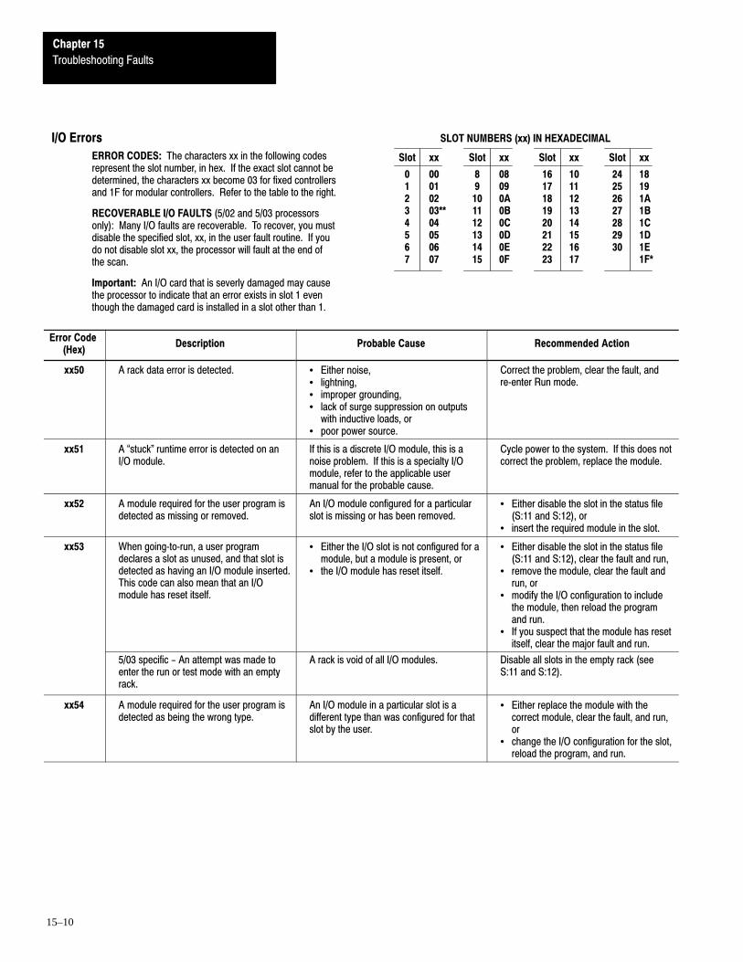
Chapter 15
Troubleshooting Faults
15–10
ERROR CODES: The characters xx in the following codesrepresent the slot number, in hex. If the exact slot cannot bedetermined, the characters xx become 03 for fixed controllersand 1F for modular controllers. Refer to the table to the right.
RECOVERABLE I/O FAULTS (5/02 and 5/03 processorsonly): Many I/O faults are recoverable. To recover, you mustdisable the specified slot, xx, in the user fault routine. If youdo not disable slot xx, the processor will fault at the end ofthe scan.
Important: An I/O card that is severly damaged may causethe processor to indicate that an error exists in slot 1 eventhough the damaged card is installed in a slot other than 1.
Slot xx
0 001 012 023 03**4 045 056 067 07
Slot xx
8 089 0910 0A11 0B12 0C13 0D14 0E15 0F
Slot xx
16 1017 1118 1219 1320 1421 1522 1623 17
Slot xx
24 1825 1926 1A27 1B28 1C29 1D30 1E
1F*
SLOT NUMBERS (xx) IN HEXADECIMALI/O Errors
Error Code (Hex)
Description Probable Cause Recommended Action
xx50 A rack data error is detected. • Either noise,• lightning,• improper grounding,• lack of surge suppression on outputs
with inductive loads, or• poor power source.
Correct the problem, clear the fault, andre�enter Run mode.
xx51 A �stuck" runtime error is detected on anI/O module.
If this is a discrete I/O module, this is anoise problem. If this is a specialty I/Omodule, refer to the applicable usermanual for the probable cause.
Cycle power to the system. If this does notcorrect the problem, replace the module.
xx52 A module required for the user program isdetected as missing or removed.
An I/O module configured for a particularslot is missing or has been removed.
• Either disable the slot in the status file(S:11 and S:12), or
• insert the required module in the slot.
xx53 When going�to�run, a user programdeclares a slot as unused, and that slot isdetected as having an I/O module inserted.This code can also mean that an I/Omodule has reset itself.
• Either the I/O slot is not configured for amodule, but a module is present, or
• the I/O module has reset itself.
• Either disable the slot in the status file(S:11 and S:12), clear the fault and run,
• remove the module, clear the fault andrun, or
• modify the I/O configuration to includethe module, then reload the programand run.
• If you suspect that the module has resetitself, clear the major fault and run.
5/03 specific - An attempt was made toenter the run or test mode with an emptyrack.
A rack is void of all I/O modules. Disable all slots in the empty rack (seeS:11 and S:12).
xx54 A module required for the user program isdetected as being the wrong type.
An I/O module in a particular slot is adifferent type than was configured for thatslot by the user.
• Either replace the module with thecorrect module, clear the fault, and run,or
• change the I/O configuration for the slot,reload the program, and run.
Chapter 15
Troubleshooting Faults
15–11
Error Code (Hex)
Description Probable Cause Recommended Action
xx55 A discrete I/O module required for the userprogram is detected as having the wrongI/O count.
This code can also mean that a specialtycard driver is incorrect.
• If this is a discrete I/O module, the I/Ocount is different from that selected inthe I/O configuration.
• If this is a specialty I/O module, the carddriver is incorrect.
• If this is a discrete I/O module, replace itwith a module having the I/O countselected in the I/O configuration. Then,clear the fault and run, or
• change the I/O configuration to matchthe existing module, then reload theprogram and run.
• If this is a specialty I/O module, refer tothe user manual for that module.
xx56 The rack configuration specified in the userprogram is detected as being incorrect.
The rack configuration specified by theuser does not match the hardware.
Correct the rack configuration, reload theprogram and run.
xx57 A specialty I/O module has not respondedto a Lock Shared Memory command withinthe required time limit.
The specialty I/O module is not respondingto the processor in the time allowed.
Cycle rack power. If this does not correctthe problem, refer to the user manual forthe specialty I/O module. You may have toreplace the module.
xx58 A specialty I/O module has generated ageneric fault. The card fault bit is set (1) inthe module's status byte.
Refer to the user manual of the specialtyI/O module.
Cycle rack power. If this does not correctthe problem, refer to the user manual forthe specialty I/O module. You may have toreplace the module.
xx59 A specialty I/O module has not respondedto a command as being completed withinthe required time limit.
A specialty I/O module did not complete acommand from the processor in the timeallowed.
Refer to the user manual for the specialtyI/O module. You may have to replace themodule.
xx5A Hardware interrupt problem. If this is a discrete I/O module, this is anoise problem. If this is a specialty I/Omodule, refer to the user manual for themodule.
Cycle rack power. Check for a noiseproblem and be sure proper groundingpractices are used. If this is a specialty I/Omodule, refer to the user manual for themodule. You may have to replace themodule.
xx5B G file configuration error - user program Gfile size exceeds the capacity of themodule.
G file is incorrect for the module in this slot. Refer to the user manual for the specialtyI/O module. Reconfigure the G file asdirected in the manual, then reload andrun.
xx5C M0-M1 file configuration error - userprogram M0-M1 file size exceeds capacityof the module.
M0-M1 files are incorrect for the module inthis slot.
Refer to the user manual for the specialtyI/O module. Reconfigure the M0-M1 filesas directed in the manual, then reload andrun.

Chapter 15
Troubleshooting Faults
15–12
Error Code (Hex)
Description Probable Cause Recommended Action
xx5D Interrupt service requested is notsupported by the processor.
The specialty I/O module has requestedservice and the processor does notsupport it.
Refer to the user manual for thespecialty I/O module to determine whichprocessors support use of the module.Change processor to one that supportsthe module.
xx5E Processor I/O driver (software) error. Corrupt processor I/O driver software. Reload program using A�B approvedAPS software.
xx60through
xx6F
Identifies an I/O module specificrecoverable major error.
- -
xx70through
xx7F
Identifies an I/O module specificnon�recoverable major error.
- -
xx90 Interrupt problem on a disabled slot. A specialty I/O module requested servicewhile a slot was disabled.
Refer to the user manual for thespecialty I/O module. You may have toreplace the module.
xx91 A disabled slot has faulted. A specialty I/O module in a disabled slothas faulted.
Cycle rack power. If this does notcorrect the problem, refer to the usermanual for the specialty I/O module.You may have to replace the module.
xx92 Invalid or non�existent module interruptsubroutine (ISR) file.
The I/O configuration/ISR file informationfor a specialty I/O module is incorrect.
Correct the I/O configuration/ISR fileinformation for the specialty I/O module.Refer to the user manual for the modulefor the correct ISR file information. Thenreload the program and run.
xx93 Unsupported I/O module specific majorerror.
The processor does not recognize theerror code from a specialty I/O module.
Refer to the user manual for thespecialty I/O module.
xx94 A module has been detected as beinginserted under power in the run or testmode.This can also mean that an I/O modulehas reset itself.
The module was inserted in the rackunder power, or the module has resetitself.
No module should ever be inserted in arack under power. If this occurs and themodule is not damaged,• Either remove the module, clear the
fault and run, or• add the module to the I/O
configuration, reference the module inthe user program where required,reload the program, and run.

A–B 16Chapter
16–1
Understanding the Fault Routine - 5/02 and 5/03 Processors
This chapter applies to the 5/02 and 5/03 processors only. It covers thefollowing topics:
• recoverable and non–recoverable faults• application examples of the fault subroutines
The 5/02 and 5/03 processors allow you to designate a subroutine file as afault routine. This file is executed when any recoverable or non-recoverableuser fault occurs. The file is not executed for non-user faults.
The fault routine gives you the option of preventing a processor shutdownwhen a specific user fault occurs. You do this by programming a laddersubroutine, then specifying that subroutine as the fault routine in Word S:29in the status file. You can handle a number of user faults in this way, as theexample on page 16–2 shows.
Status File Data Saved
Data in the following words is saved on entry to the fault routine subroutineand re-written upon exiting the subroutine.
• S:0 Arithmetic flags• S:13 and S:14 Math register• S:24 Index register
Faults are classified as recoverable and non-recoverable user faults, andnon-user faults. A complete list of faults appears in chapter 1 of this manual.
Non-User Fault Non-Recoverable User Fault Recoverable User Fault
The Fault Routine does notexecute.
The Fault Routine executes for1 pass. Note: You may initiatea MSG instruction to anothernode to identify the faultcondition of the processor.
The Fault Routine may clearthe fault by clearing bit S:1/13.
Overview of the Fault Routine
Recoverable and Non-Recoverable User Faults
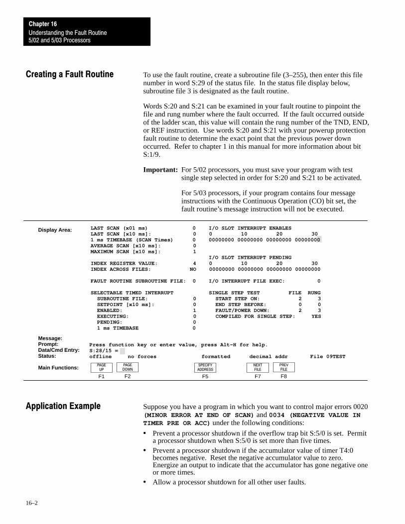
5/02 and 5/03 Processors
Chapter 16
Understanding the Fault Routine
16–2
To use the fault routine, create a subroutine file (3–255), then enter this filenumber in word S:29 of the status file. In the status file display below,subroutine file 3 is designated as the fault routine.
Words S:20 and S:21 can be examined in your fault routine to pinpoint thefile and rung number where the fault occurred. If the fault occurred outsideof the ladder scan, this value will contain the rung number of the TND, END,or REF instruction. Use words S:20 and S:21 with your powerup protectionfault routine to determine the exact point that the previous power downoccurred. Refer to chapter 1 in this manual for more information about bitS:1/9.
Important: For 5/02 processors, you must save your program with testsingle step selected in order for S:20 and S:21 to be activated.
For 5/03 processors, if your program contains four messageinstructions with the Continuous Operation (CO) bit set, thefault routine’s message instruction will not be executed.
LAST SCAN (x01 ms) 0 I/O SLOT INTERRUPT ENABLESLAST SCAN [x10 ms]: 0 0 10 20 301 ms TIMEBASE (SCAN Times) 0 00000000 00000000 00000000 00000000AVERAGE SCAN [x10 ms]: 0 MAXIMUM SCAN [x10 ms]: 1
I/O SLOT INTERRUPT PENDINGINDEX REGISTER VALUE: 4 0 10 20 30INDEX ACROSS FILES: NO 00000000 00000000 00000000 00000000 FAULT ROUTINE SUBROUTINE FILE: 0 I/O INTERRUPT FILE EXEC: 0
SELECTABLE TIMED INTERRUPT SINGLE STEP TEST FILE RUNG SUBROUTINE FILE: 0 START STEP ON: 2 3 SETPOINT [x10 ms]: 0 END STEP BEFORE: 0 0 ENABLED: 1 FAULT/POWER DOWN: 2 3 EXECUTING: 0 COMPILED FOR SINGLE STEP: YES PENDING: 0 1 ms TIMEBASE 0
Display Area:
F7F5 F8
NEXTFILE
SPECIFYADDRESS
Press function key or enter value, press Alt–H for help.S:28/15 = offline no forces formatted decimal addr File 09TEST
Message:Prompt:Data/Cmd Entry:Status:
Main Functions:PREVFILE
F1 F2
PAGEUP
PAGEDOWN
Suppose you have a program in which you want to control major errors 0020(MINOR ERROR AT END OF SCAN) and 0034 (NEGATIVE VALUE INTIMER PRE OR ACC) under the following conditions:
• Prevent a processor shutdown if the overflow trap bit S:5/0 is set. Permita processor shutdown when S:5/0 is set more than five times.
• Prevent a processor shutdown if the accumulator value of timer T4:0becomes negative. Reset the negative accumulator value to zero.Energize an output to indicate that the accumulator has gone negative oneor more times.
• Allow a processor shutdown for all other user faults.
Creating a Fault Routine
Application Example
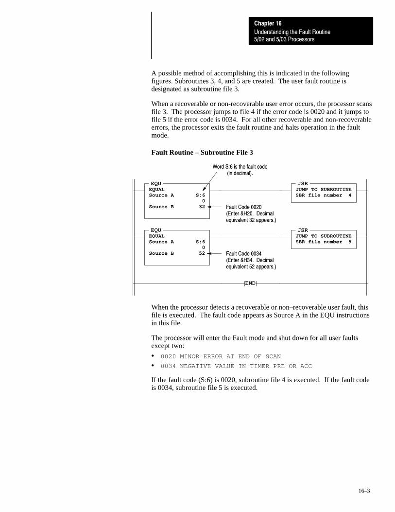
5/02 and 5/03 Processors
Chapter 16
Understanding the Fault Routine
16–3
A possible method of accomplishing this is indicated in the followingfigures. Subroutines 3, 4, and 5 are created. The user fault routine isdesignated as subroutine file 3.
When a recoverable or non-recoverable user error occurs, the processor scansfile 3. The processor jumps to file 4 if the error code is 0020 and it jumps tofile 5 if the error code is 0034. For all other recoverable and non-recoverableerrors, the processor exits the fault routine and halts operation in the faultmode.
Fault Routine – Subroutine File 3
END
EQUEQUALSource A S:6
0Source B 32 Fault Code 0020
(Enter &H20. Decimalequivalent 32 appears.)
JSRJUMP TO SUBROUTINESBR file number 4
JSRJUMP TO SUBROUTINESBR file number 5
EQUEQUALSource A S:6
0Source B 52 Fault Code 0034
(Enter &H34. Decimalequivalent 52 appears.)
Word S:6 is the fault code(in decimal).
When the processor detects a recoverable or non–recoverable user fault, thisfile is executed. The fault code appears as Source A in the EQU instructionsin this file.
The processor will enter the Fault mode and shut down for all user faultsexcept two:
• 0020 MINOR ERROR AT END OF SCAN
• 0034 NEGATIVE VALUE IN TIMER PRE OR ACC
If the fault code (S:6) is 0020, subroutine file 4 is executed. If the fault codeis 0034, subroutine file 5 is executed.

5/02 and 5/03 Processors
Chapter 16
Understanding the Fault Routine
16–4
Subroutine File 4 – Executed for Error 0020
END
SBRSUBROUTINE
RETRETURN
GRTGREATER THANSource A C5:0.ACC
0Source B 5
(CU)
(DN)
CTUCOUNT UPCounter C5:0Preset 120Accum 0
(U)S:5
0
] [S:5
0(U)
C5:0
CU
(U)S:1
13
RETRETURN
] [S:5
0
If the overflow trap bit S:5/0 is set, counter C5:0 will increment.
If the count of C5:0 is 5 or less, the overflow trap S:5/0 will be cleared, themajor error halted bit S:1/13 will be cleared, and the processor will remain inthe REM Run mode. Fault code 0020 will be indicated in the status display.If the count is greater than 5, the processor will set S:5/0 and S:1/13 andenter the Fault mode.
This subroutine file is also executed if the control register error bit S:5/2 isset. In this case, the processor is placed in the Fault mode.

5/02 and 5/03 Processors
Chapter 16
Understanding the Fault Routine
16–5
ARITHMETIC FLAGS S:0 Z:0 V:0 C:0
PROCESSOR STATUS 00000000 00000000 SUSPEND CODE 0PROCESSOR STATUS 00000000 11100110 SUSPEND FILE 0PROCESSOR STATUS 00000000 00100010 WATCHDOG [x 10 ms] 10MINOR FAULT 00000000 00000000 LAST SCAN [x 10 ms] 1FAULT CODE 0020 FREE RUNNING CLOCK 00000000 00000000FAULT DESCRIPTION: MINOR ERROR AT END OF SCAN
MATH REGISTER 0000 0000
ACTIVE NODE LIST (CHANEL 1) I/O SLOT ENABLES0 10 20 30 0 10 20 3011000000 00000000 00000000 00000000 11111111 11111111 11111111 11111111
PROCESSOR BAUD RATE (CHANNEL 1) 19200 PROCESSOR ADDRESS (CHANNEL 1): 1
Fault code anddescription areindicated.
S:1/13 Cleared
S:5/0 Cleared
F8
KEYSWITCH IS IN RUN, CLEARING FAULT CAUSES PROCESSOR TO GO TO RUN MODEClear Major Fault?S:28/15 = offline no forces formatted decimal addr File 09TEST
Message:Prompt:Data/Cmd Entry:Status:
Main Functions:YES
F8
NO
Status File Display - At 1st through 5th overflow (S:5/0) occurrences
Subroutine File 5 – Executed for Error 0034
END
(U)S:1
13
RETRETURN
SBRSUBROUTINE
LESLESS THANSource A T4:0.ACC
0Source B 0
CLRCLEARDest T4:0.ACC
0
( )O:3.0
3
If the accumulator value of timer T4:0 is negative, the major error halted bit,S:1/13 is unlatched, preventing the processor from entering the Fault mode.At the same time, the accumulator value T4:0 ACC is cleared to zero andoutput O:3.0/3 is energized. Fault code 0034 will be indicated in the statusfile display.
If the preset of timer T4:0 is negative, S:1/13 will remain set and theprocessor will enter the Fault mode (O:3.0/3 will be reset if previously set).Also, if either the preset or accumulator value of any other timer in theprogram is negative, S:1/13 will be set and the processor will enter the Faultmode. If previously set, O:3.0/3 will be reset.

A–B 17Chapter
17–1
Understanding the Discrete Input Interrupt -5/03 Processor Only
This chapter applies to the 5/03 processor only. It covers the followingtopics:
• programming for the Discrete Input Interrupt (DII) function• DII operation• DII parameters
Use the Discrete Input Interrupt (DII) for high–speed processing applicationsor any application that needs to respond to an event quickly. This instructionallows the 5/03 processor to execute a ladder subroutine when the input bitpattern of a discrete I/O card matches a compare value that you programmed.
The status file contains six bit values and six word values used to programand monitor the DII function. The DII does not require ladder logicinstructions for configuration. You program the DII to examine the input bitpattern of any single I/O slot which contains any discrete input card (IG16,IV16, IB8, IB32, etc.). When the input bit pattern matches the comparevalue, the accumulator is incremented. The DII accumulator counts to thepreset value, and once the interrupt is generated, it immediately wrapsaround and begins counting again at zero.
While scanning the DII subroutine, you can reconfigure the DII to look foran entirely different event. This facilitates DII sequencing. The DII can beprogrammed to compare each input point to either a high (1) or low (0) state.The accumulator is incremented on the input transition that causes the inputpoints to match the compare value.
We recommend programming Immediate I/O instructions (IOM and IIM) inthe DII subroutine. This allows the subroutine to have access to physicalmachine states.
Basic Programming Procedure for the DII Function
To use the DII function with your main program file, do the following:
1. Create a subroutine file (range is from 3 to 255) and enter the desiredladder rungs. This is your DII subroutine file.Creating a subroutine file is discussed in the Advanced ProgrammingSoftware User Manual, Catalog Number 1747–NM002.
2. Enter the Input Slot number (Word S:47).
3. Enter the Bit Mask (Word S:48).
4. Enter the Compare Value (Word S:49).
5. Enter the Preset Value (Word S:50).
Overview of the Discrete InputInterrupt

5/03 Processors
Chapter 17
Understanding the Discrete Input Interrupt
17–2
6. Enter the DII subroutine file number in word S:46 of the status file. (Seepage 1–38.) A file number of zero disables the DII function.
Important: PLC users – The main difference between the DII and the PLC5/40 PII is that the DII requires all stated transitions to occurprior to generating a down count; while the PII requires thatonly one of the stated transitions occur. Also, the PLC term“down count” is referred to as “preset” in the DII.
Example
The DII can be programmed to count items on a high–speed conveyer. Eachtime 100 items pass a photo–switch, the DII subroutine is executed. The DIIsubroutine then uses Immediate I/O instructions to package the products.
After you restore your program and enter the REM Run mode, the DII beginsoperation as follows:
Counter Mode
This mode is active when the preset value (S:50) contains a value greaterthan 1.
1. The DII reads the first byte of input data of a selected discrete input cardat least once every 100µs.➀
2. When the input data matches the programmed masked value, theaccumulator is incremented by one. The next count occurs when inputdata transitions to non–matched and then back to matched.
3. When the accumulator reaches or exceeds the preset value, between 1 and65,535, the interrupt is generated.
4. The DII subroutine is executed.
5. The cycle repeats.
Event Mode
This mode is active when the preset value (S:50) contains a 0 or 1.
1. The DII reads the first byte of input data of a selected discrete input cardat least once every 100µs.➀
2. When the input data matches the programmed masked value, the interruptis generated.
3. The DII subroutine is executed.➁
4. The cycle repeats.➀
➀ You must add interrupt latency time to the final transition or count that causes the interruptsubroutine to execute.
➁ The DII continues to compare the input data to the programmed masked value while executingthe DII subroutine.
Operation

5/03 Processors
Chapter 17
Understanding the Discrete Input Interrupt
17–3
DII Subroutine Content
For identification of your DII subroutine, use the INT instruction as the firstinstruction in your first rung.
The DII subroutine contains the rungs of your application logic. You canprogram any instruction inside the DII subroutine except a TND, REF, orSVC instruction. IIM or IOM instructions are needed in a DII subroutine ifyour application requires immediate update of input or output points. Endthe DII subroutine with an RET instruction.
JSR stack depth is limited to 3. You may call other subroutines to a level 3deep from an DII subroutine.
Interrupt Latency and Interrupt Occurrences
Interrupt latency is the interval between DII detection and the start of theinterrupt subroutine. DII interrupts can occur at any point in your program,but not necessarily at the same point on successive interrupts. Interrupts canoccur between instructions in your program, inside the I/O scan (betweenslots), or between the servicing of communications packets. The table belowshows the interaction between an interrupt and the processor operating cycle.
5/02 I/O Interrupts5/03 I/O Interrupts with
Bit S:33/8 set5/03 I/O Interrupts with
Bit S:33/8 cleared
Between slot updates Between word updates Between slot updates
Between instruction updates Between word updates Between rung updates
Between slot updates Between word updates Between slot updates
Between communicationpackets
Between word packet updatesBetween communicationpackets
At start and end Between word updates Between word updates
If an interrupt occurs while the 5/03 processor is performing a multi–wordslot update and your interrupt subroutine accesses that same slot, themulti–word transfer finishes to completion prior to performing the interruptsubroutine slot access.
Note that DII execution time adds directly to the overall scan time. Duringthe latency period, the processor is performing operations that cannot bedisturbed by the DII interrupt function. The Discrete Input Interrupt LatencyBit (S:33/8) functions as follows:
• When the bit is set (1) interrupts are serviced within 500µs.• When the bit is clear (0), 500µs servicing is not expected. When S:33/8 is
clear (0), user interrupts occur between rungs and I/O slot updates.
Processor Overhead
Communications
Output Scan
Program Scan
Input Scan
Events in the Processor Operating Cycle
5/03 Processors
Chapter 17
Understanding the Discrete Input Interrupt
17–4
The default state is cleared (0). To determine the interrupt latency withS:33/8 clear, you must calculate the execution time of each and every rung inyour program. Refer to appendix B in the Advanced Programming SoftwareUser Manual, Catalog Number 1747–NM002 for more information on howto calculate the interrupt latency.
Interrupt Priorities
Interrupt priorities for 5/03 processors are:
1. fault routine
2. Discrete Input Interrupt (DII)
3. STI Subroutine
4. I/O Interrupt Subroutine
An executing interrupt subroutine can only be interrupted by the faultroutine.
Status File Data Saved
Data in the following words is saved on entry to the DII subroutine andre-written upon exiting the DII subroutine.
• S:0 Arithmetic flags• S:13 and S:14 Math register• S:24 Index register
Reconfigurability
You can reconfigure the DII entirely or in part, depending on the particularparameter(s) you choose. You can reconfigure some of the parameterssimply by writing the new value over the old value. Other values require youto set the reconfiguration bit in addition to writing the new value. The DII isnon–retentive and always reconfigures itself upon entry into the REM Runmode. Refer to the next section “DII Parameters” for details onreconfiguring each parameter.

5/03 Processors
Chapter 17
Understanding the Discrete Input Interrupt
17–5
The following parameters are associated with the DII function. Theseparameters have status file addresses that are described here and also inchapter 1 of this manual.
• Bit S:2/11 DII Pending Bit– Read only. When set, this bit indicates thatthe DII accumulator (S:52) equals the DII preset (S:50) and the ladder filenumber specified by the DII file number (S:46) is waiting to be executed.It is cleared when the DII file number (S:46) begins executing, or on exitfrom the REM Run or REM Test mode.
• Bit S:2/12 DII Enable Bit – Read/write. To program this feature, use thedata monitor function to set/clear this bit, or address this bit with yourladder program. This bit is set in its default condition. If set, it allowsexecution of the DII subroutine if the DII file (S:46) is non–zero. If clear,when the interrupt occurs, the DII subroutine will not execute and the DIIPending bit is be set. The DII function continues to run anytime the DIIfile (S:46) is non–zero. If the pending bit is set, the enable bit isexamined at the next end of scan.
• Bit S:2/13 DII Executing Bit – Read only. When set, this bit indicatesthat the DII interrupt has occurred and the DII subroutine is currentlybeing executed. This bit is cleared on completion of the DII routine,powerup, or REM Run mode entry.
• Bit S:5/12 DII Overflow Bit – Read/write. This bit is set whenever theDII interrupt occurs while still executing the DII subroutine or wheneverthe DII interrupt occurs while pending or disabled.
• Bit S:33/10 Reconfigure – Read/write. When this bit is set (1), itindicates that at the next end of scan (END, TND, or REF), fault routineexit, STI ISR exit, Event ISR exit, or next DII ISR exit the:– DII accumulator is cleared,– values at status words S:47 to S:50 are applied,– the pending bit is cleared, and– the DII Reconfigure bit is cleared.
• Bit S:36/8 DII Lost – Read/write. This bit is set if a DII interrupt occurswhile the DII Pending bit is set.
• Word S:46 File Number – Read/write. You enter a program file number(3 to 255) to be used as the discrete input interrupt subroutine. Write a 0value to disable the function. This bit is applied upon detection of DIIReconfigure bit, each DII ISR exit, and each end of scan (END, TND, orREF). A zero disables operation.
• Word S:47 Slot Number – Read/write. You enter the slot number (1 to30) to be used as the discrete input interrupt subroutine. A zero valuedisables the function. This is applied on detection of the DII Reconfigurebit, or on entry into the REM Run mode.
DII Parameters

5/03 Processors
Chapter 17
Understanding the Discrete Input Interrupt
17–6
• Word S:48 Bit Mask – Read/write. You enter the bit mapped value thatcorresponds to the bits you wish to monitor on the discrete I/O module.Only bits 0 to 7 are used in the DII function. Setting a bit indicates thatyou wish to include the bit in the comparison of the discrete I/O card’s bitpattern to the DII compare value (S:49). This is applied on detection ofthe DII Reconfigure bit, each DII ISR exit, and at each end of scan (END,TND, or REF).
• Word S:49 Compare Value – Read/write. You enter a bit mapped valuethat corresponds to the bit pattern that must occur on the discrete I/O cardfor a count or interrupt to occur. Only bit 0 to 7 are used in the DIIfunction. The bit must be set (1) or cleared (0) in order to satisfy thecompare condition for that bit. An interrupt or count will be generatedupon the last bit transition of the compare value. This is applied ondetection of DII Reconfigure bit, each DII ISR exit, and at each end ofscan (END, TND, or REF).To provide protection from inadvertent data monitor alteration of yourselection, program an unconditional MOV instruction containing thepreset value of the DII to S:50.
• Word S:50 Preset – Read/write. When this value is equal to 0 or 1, aninterrupt is generated each time the comparison specified in words S:48and S:49 is satisfied. When this value is between 2 and 32767, a countwill occur each time the bit comparison is satisfied. An interrupt will begenerated when the accumulator value reaches 1 or exceeds the presetvalue. This is applied on detection of DII Reconfigure bit, each DII ISRexit, and at each end of scan (END, TND, or REF).To provide protection from inadvertent data monitor alteration of yourselection, program an unconditional MOV instruction containing thedown count value of the DII to S:50.
• Word S:51 Return Mask – Read only. The Return Mask is updatedimmediately preceding entry into the DII subroutine. This value containsthe bit map of the last bit transition that caused the interrupt. If more thanone bit transitions in the same 100µs DII sample period, it will beincluded in the return mask. This bit is cleared by the processor on exitfrom the DII subroutine. Use this value to validate the last interrupttransition that caused the input pattern to match the compare value. Orwhen dynamically reconfiguring (sequencing) the DII, use this valueinside of your DII’s subroutine to help determine/validate its position ofthe sequence.

5/03 Processors
Chapter 17
Understanding the Discrete Input Interrupt
17–7
You can enter and monitor DII parameters at the status file display of APSsoftware. There are four displays associated with the DII function. Refer topages 17–5 and 17–6 for descriptions of the DII parameters.
ARITHMETIC FLAGS S:0 Z:0 V:0 C:0
PROCESSOR STATUS 00000000 00000000 SUSPEND CODE 0PROCESSOR STATUS 00000000 00000001 SUSPEND FILE 0PROCESSOR STATUS 00000000 00000000 WATCHDOG [x10 ms] 10MINOR FAULT 00000000 00000000 LAST SCAN [x10 ms] 0FAULT CODE 0000 FREE RUNNING CLOCK 00000000 00000000FAULT DESCRIPTION:
MATH REGISTER 0000 0000
ACTIVE NODE LIST (CHANNEL 1) I/O SLOT ENABLES0 10 20 30 0 10 20 3011000000 00000000 00000000 00000000 11111111 11111111 11111111 11111111
PROCESSOR BAUD RATE (CHANNEL 1) 19200 PROCESSOR ADDRESS (CHANNEL 1) 1
Press function key or enter value, press Alt–H for help.S:0/0 = offline no forces formatted decimal addr File 09TEST
Message:Prompt:Data/Cmd Entry:Status:
Main Functions:
F7F5
NEXTFILE
SPECIFYADDRESS
F9 F10F8
CLR MINFAULT
CLR MAJFAULT
PREVFILE
Display Area:
F1
PAGEUP
F2
PAGEDOWN
LAST SCAN (x01 ms) 0 I/O SLOT INTERRUPT ENABLESLAST SCAN [x10 ms]: 0 0 10 20 301 ms TIMEBASE (SCAN Times) 0 00000000 00000000 00000000 00000000AVERAGE SCAN [x10 ms]: 0 MAXIMUM SCAN [x10 ms]: 1
I/O SLOT INTERRUPT PENDINGINDEX REGISTER VALUE: 4 0 10 20 30INDEX ACROSS FILES: NO 00000000 00000000 00000000 00000000 FAULT ROUTINE SUBROUTINE FILE: 0 I/O INTERRUPT FILE EXEC: 0
SELECTABLE TIMED INTERRUPT SINGLE STEP TEST FILE RUNG SUBROUTINE FILE: 0 START STEP ON: 2 3 SETPOINT [x10 ms]: 0 END STEP BEFORE: 0 0 ENABLED: 1 FAULT/POWER DOWN: 2 3 EXECUTING: 0 COMPILED FOR SINGLE STEP: YES PENDING: 0 1 ms TIMEBASE 0
Display Area:
F7F5 F8
NEXTFILE
SPECIFYADDRESS
Press function key or enter value, press Alt–H for help.S:28/15 = offline no forces formatted decimal addr File 09TEST
Message:Prompt:Data/Cmd Entry:Status:
Main Functions:PREVFILE
F1 F2
PAGEUP
PAGEDOWN
Status File Display

5/03 Processors
Chapter 17
Understanding the Discrete Input Interrupt
17–8
Additional 5/03 Status File Displays
Refer to pages 17–5 and 17–6 for descriptions of the DII parameters.
EXT PROCESSOR STATUS 0000000 00000000 REAL TIME CLOCK DATE: 10–18–1992EXT MINOR FAULT 0000000 00000000 TIME: 2:15.34
DISCRETE INPUT INTERRUPT SUBROUTINE FILE: 3 MASK: 00000001 INPUT SLOT: 1 COMPARE VALUE: 00000001 ENABLED 1 PRESET: 1 EXECUTING: 0 RETURN MASK: 00000000 PENDING: 0 ACCUMULATOR: 0 OVERFLOW: 0 LAST SCAN [ms]: 0
MAX. SCAN [ms]: 0
PROCESSOR OPERATING SYSTEM USER PROGRAM CATALOG #: 0 CATALOG #: 0 FUNCTIONAL TYPE: 0 SERIES: 0 SERIES: 0 FUNCTIONAL INDEX: 0 REVISION: 0 F.R.N.: 0 USER RAM SIZE: 0 FLASH EEPROM SIZE: 0
Display Area:
Press function key or enter value, press Alt–H for help.S:0/0 = offline no forces formatted decimal addr File 09TEST
Message:Prompt:Data/Cmd Entry:Status:
Main Functions:
F7F5 F8
NEXTFILE
SPECIFYADDRESS
PREVFILE
F1 F2
PAGEUP
PAGEDOWN
CHANNEL 0 ACTIVE NODE TABLE
0–31 00000000 00000000 00000000 00000000 32–63 00000000 00000000 00000000 00000000 64–95 00000000 00000000 00000000 00000000 96–127 00000000 00000000 00000000 00000000128–159 00000000 00000000 00000000 00000000160–191 00000000 00000000 00000000 O0000000192–223 00000000 00000000 00000000 00000000224–255 00000000 00000000 00000000 00000000
Display Area:
0 10 20 30
Press function key or enter value, press Alt–H for help.S:0/0 = offline no forces formatted decimal addr File 09TEST
Message:Prompt:Data/Cmd Entry:Status:
Main Functions:
F7F5 F8
NEXTFILE
SPECIFYADDRESS
PREVFILE
F1 F2
PAGEUP
PAGEDOWN
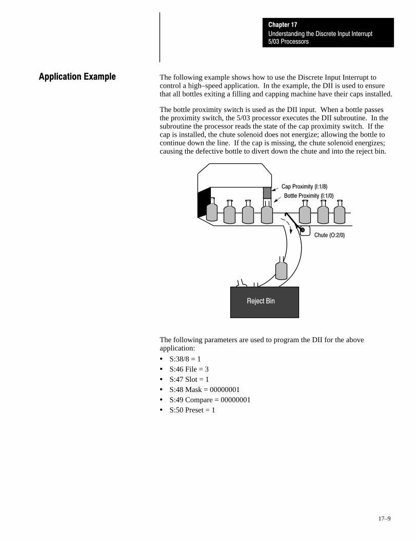
5/03 Processors
Chapter 17
Understanding the Discrete Input Interrupt
17–9
The following example shows how to use the Discrete Input Interrupt tocontrol a high–speed application. In the example, the DII is used to ensurethat all bottles exiting a filling and capping machine have their caps installed.
The bottle proximity switch is used as the DII input. When a bottle passesthe proximity switch, the 5/03 processor executes the DII subroutine. In thesubroutine the processor reads the state of the cap proximity switch. If thecap is installed, the chute solenoid does not energize; allowing the bottle tocontinue down the line. If the cap is missing, the chute solenoid energizes;causing the defective bottle to divert down the chute and into the reject bin.
Cap Proximity (I:1/8)
Bottle Proximity (I:1/0)
Chute (O:2/0)
Reject Bin
The following parameters are used to program the DII for the aboveapplication:
• S:38/8 = 1• S:46 File = 3• S:47 Slot = 1• S:48 Mask = 00000001• S:49 Compare = 00000001• S:50 Preset = 1
Application Example

5/03 Processors
Chapter 17
Understanding the Discrete Input Interrupt
17–10
Ladder Diagram for the Bottling Application
Update chute position.
Update chuteposition.
INTI/O INTERRUPT
]/[I:1.0
8
RETRETURN
END
IIMIMMEDIATE IN w MASKSlot I:1.0Mask 0100
Rung 3:0
This rung gets the state of the proximity switch to sense the present or absent of a bottle cap.
Rung 3:1
If a bottle cap is present, and the chute is in the reject position, set the chute position to normal.
] [I:1.0
8] [
O:2.0
0(U)
O:2.0
0
IOMIMMEDIATE OUT w MASKSlot O:2.0Mask 0001
Rung 3:2
If no bottle cap is present, set the chute position to reject.
(L)O:2.0
0
IOMIMMEDIATE OUT w MASKSlot O:2.0Mask 0001
Rung 3:3
Rung 3:4
Bit 8 is the cap proximity switch.
Move chute tonormal position.
If prox. switch detectsbottle cap installed
And if the chute is inthe reject position
Move chute toreject position.
If prox switch detectsa missing bottle cap

A–B 18Chapter
18–1
Understanding Selectable Timed Interrupts -5/02 and 5/03 Processors
This chapter applies to the 5/02 and 5/03 processors only. It covers thefollowing topics:
• Selectable Timed Interrupts (STI) operation• STI parameters• STD and STE instructions• STS instruction
Use the Selectable Timed Interrupt (STI) function with 5/02 and 5/03processors. This function allows you to interrupt the scan of the mainprogram file automatically, on a periodic basis, in order to scan a specifiedsubroutine file.
Basic Programming Procedure for the STI Function
To use the STI function with your main program file:
1. Create a subroutine file (range is from 3 to 255) and enter the desiredladder rungs. This is your STI subroutine file.Creating a subroutine file is discussed in the Advanced ProgrammingSoftware User Manual, Catalog Number 1747–NM002.
2. Enter the STI subroutine file number in word S:31 of the status file.Refer to page 1–33 in this manual for more information. A file number ofzero disables the STI function.
3. Enter the setpoint (the time between successive interrupts) in word S:30of the status file. Refer to page 1–33 in this manual for more information.
• For 5/02 and 5/03 processors, the range is 10–2550 ms (entered in10 ms increments). A setpoint of zero disables the STI function.
• The 5/03 processor has an additional range from 1–32,767 ms (enteredin 1 ms increments). A setpoint of zero disables the STI function.Refer to chapter 1 in this manual for more information about the STIResolution bit S:2/10.
Important: The setpoint value must be a longer time than the executiontime of the STI subroutine file, or a minor error will occur. Forthe 5/02 processor the S:5/10 Overrun bit is set. Additionally,for the 5/03 processor the S:36/9 STI Lost bit may be set.
STI Overview
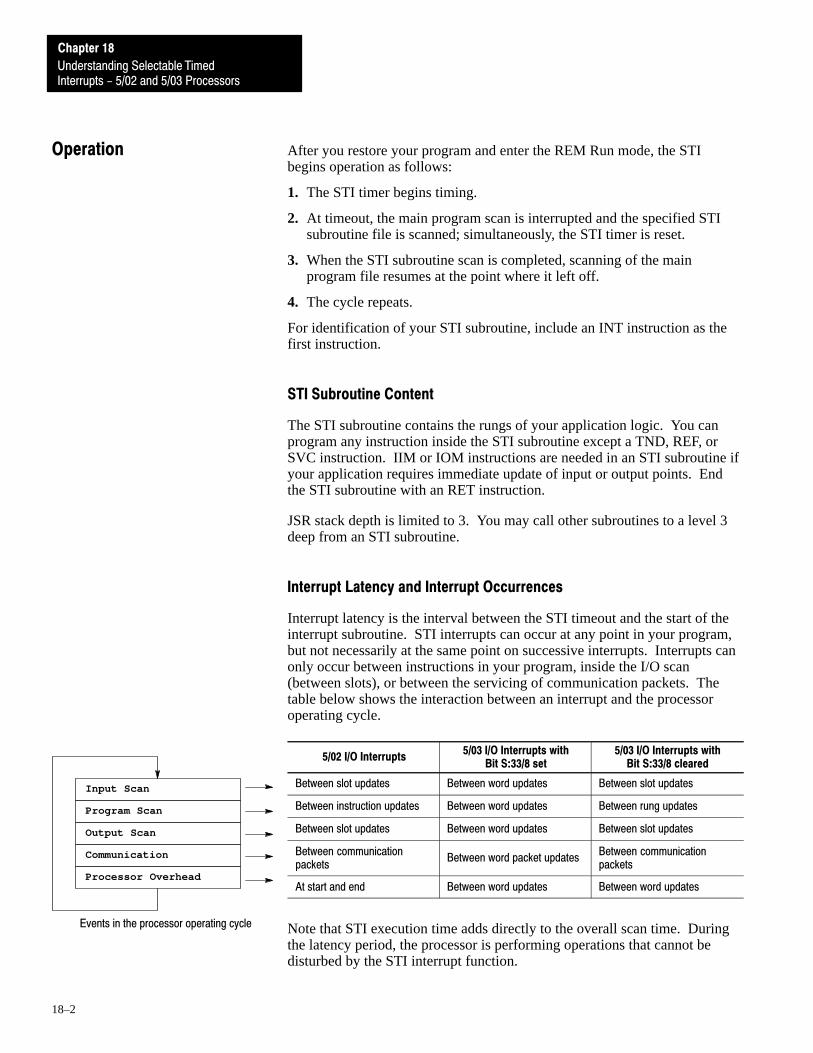
Interrupts - 5/02 and 5/03 Processors
Chapter 18
Understanding Selectable Timed
18–2
After you restore your program and enter the REM Run mode, the STIbegins operation as follows:
1. The STI timer begins timing.
2. At timeout, the main program scan is interrupted and the specified STIsubroutine file is scanned; simultaneously, the STI timer is reset.
3. When the STI subroutine scan is completed, scanning of the mainprogram file resumes at the point where it left off.
4. The cycle repeats.
For identification of your STI subroutine, include an INT instruction as thefirst instruction.
STI Subroutine Content
The STI subroutine contains the rungs of your application logic. You canprogram any instruction inside the STI subroutine except a TND, REF, orSVC instruction. IIM or IOM instructions are needed in an STI subroutine ifyour application requires immediate update of input or output points. Endthe STI subroutine with an RET instruction.
JSR stack depth is limited to 3. You may call other subroutines to a level 3deep from an STI subroutine.
Interrupt Latency and Interrupt Occurrences
Interrupt latency is the interval between the STI timeout and the start of theinterrupt subroutine. STI interrupts can occur at any point in your program,but not necessarily at the same point on successive interrupts. Interrupts canonly occur between instructions in your program, inside the I/O scan(between slots), or between the servicing of communication packets. Thetable below shows the interaction between an interrupt and the processoroperating cycle.
5/02 I/O Interrupts5/03 I/O Interrupts with
Bit S:33/8 set5/03 I/O Interrupts with
Bit S:33/8 cleared
Between slot updates Between word updates Between slot updates
Between instruction updates Between word updates Between rung updates
Between slot updates Between word updates Between slot updates
Between communicationpackets
Between word packet updatesBetween communicationpackets
At start and end Between word updates Between word updates
Note that STI execution time adds directly to the overall scan time. Duringthe latency period, the processor is performing operations that cannot bedisturbed by the STI interrupt function.
Operation
Processor Overhead
Communication
Output Scan
Program Scan
Input Scan
Events in the processor operating cycle

Interrupts - 5/02 and 5/03 Processors
Chapter 18
Understanding Selectable Timed
18–3
Latency periods are:
• 5/02 series B processor interrupts are serviced within 3.7 ms maximum.• 5/02 series C processor and later interrupts are serviced within 2.4 ms
maximum.• 5/03 processor – If an interrupt occurs while the 5/03 processor is
performing a multi–word slot update and your interrupt subroutineaccesses that same slot, the multi–word transfer finishes to completionprior to performing the interrupt subroutine slot access. The 5/03processor Interrupt Latency Bit (S:33/8) functions as follows:– When the bit is set (1) interrupts are serviced within 500µs.– When the bit is clear (0), INTs are serviced per rung, slot, and packet
execution time.
The default state is cleared (0). To determine the interrupt latency withS:33/8 clear, you must calculate the execution time of each and everyrung in your program. Use the longest calculated execution time plus500µs as your maximum interrupt latency. Refer to appendix B in theAdvanced Programming Software User Manual, Catalog Number1747–NM002 for more information on how to calculate the interruptlatency.
Interrupt Priorities
Interrupt priorities for 5/02 and 5/03 processors are:
5/02 Processor 5/03 Processor
1. Fault Routine 1. Fault Routine
2. STI Subroutine 2. Discrete Input Interrupt (DII)
3. Interrupt Subroutine (ISR) 3. STI Subroutine
4. Interrupt Subroutine (ISR)
An executing interrupt can only be interrupted by an interrupt having higherpriority.
Status File Data Saved
Data in the following words is saved on entry to the STI subroutine andre-written upon exiting the STI subroutine.
• S:0 Arithmetic flags• S:13 and S:14 Math register• S:24 Index register

Interrupts - 5/02 and 5/03 Processors
Chapter 18
Understanding Selectable Timed
18–4
The following parameters are associated with the STI function. Theseparameters have status file addresses that are described here and also inchapter 1 of this manual.
• Word S:31 STI file number – This can be any number from 3–255. Avalue of zero disables the STI function. An invalid number generatesfault 0023.
• Word S:30 Setpoint – This is the time between the starting point ofsuccessive scans of the STI file. It can be any value from 10 to 2550milliseconds. You enter a value of 1 to 255, which results in a10–2550 ms setpoint. A value of zero disables the STI function. Aninvalid time generates fault 0024.If the STI is initiated while in the REM Run mode by loading the statusregisters, the interrupt will start timing from the end of the program scanin which the status registers were loaded.
5/03 specific – If S2:2/10 is set, time is in 1 ms increments. If this bit isclear, time is in 10 ms increments.
Word S:2
• Bit S:2/0 STI Pending Bit – Read only. This bit is set when the STItimer has timed out while the STI file is either being scanned or disabled.This bit is reset upon the start of the STI routine, execution of an STS orSTE instruction, powerup, and exit from the REM Run mode.
5/02 specific – The STI pending bit will not be set if the STI timer expireswhile executing the fault routine.5/03 specific – This bit is also set if the STI timer expires while executingthe DII subroutine or fault routine.
• Bit S:2/1 STI Enable Bit – The default value is 1 (set). When a filenumber between 3 and 255 is present in word S:31 and a setpoint valuebetween 1 and 255 is present in word S:30, a set enable bit allowsscanning of the STI file. If the bit is reset by an STD instruction,scanning of the STI file no longer occurs. If the bit is set by an STE orSTS instruction, scanning is again allowed. The enable bit onlyenables/disables the scanning of the STI subroutine. It does not affect theSTI timer. The STS instruction affects both the enable bit and the STItimer. The default state is enabled. If this bit is set or reset using theSTE, STD, or STS instruction, enable/disable takes effect immediately. Ifthis bit is set in the user program using an instruction other than STE,STD, or STS, it takes effect at the next end of scan.
5/02 specific – If this bit is set or reset by the user program or comms., itwill not take effect until the next end of scan.5/03 specific – If this bit is set or reset by the user program or comms., itwill take effect upon the STI timer expiration or next end of scan (whichever occurs first).
• Bit S:2/2 STI Executing Bit – Read only. This bit is set when the STIfile is being scanned and cleared when the scan is completed. The bit isalso cleared on powerup and entry into the REM Run mode.
STI Parameters

Interrupts - 5/02 and 5/03 Processors
Chapter 18
Understanding Selectable Timed
18–5
• Bit S:2/10 STI Resolution Selection Bit (5/03 only) – Read/write. Thisbit is clear by default. When clear, this bit selects a 10 ms increment forthe STI Setpoint (S:30) value. When set, this bit selects a 1 ms incrementfor the STI Setpoint (S:30) value. To program this feature, use the datamonitor function to set/clear this bit, or address this bit with your ladderprogram.This bit is user configurable and takes effect on a REM PROG to REMRUN mode transition. This bit takes effect immediately if the STSinstruction is executed.
Word 5
• Bit S:5/10 Overrun Bit – Read/write. This minor error bit is setwhenever the STI timer expires while the STI routine is executing ordisabled while the pending bit is set. When this occurs, the STI timercontinues to operate at the rate present in word S:30. If the overrun bitbecomes set, take the corrective action your application dictates, thenclear the bit.
Word 36
• Word S:36/9 STI Lost Bit (5/03 only) – Read/write. This bit is setanytime an STI interrupt occurs while the STI Pending bit is also set.When set, you are notified that a STI interrupt has been lost. Forexample, the interrupt is lost because a previous interrupt was alreadypending and waiting execution. Examine this bit in your user programand take appropriate action if your application cannot tolerate thiscondition. Then clear this bit with your user program in order to preparefor the next possible occurrence of this error.
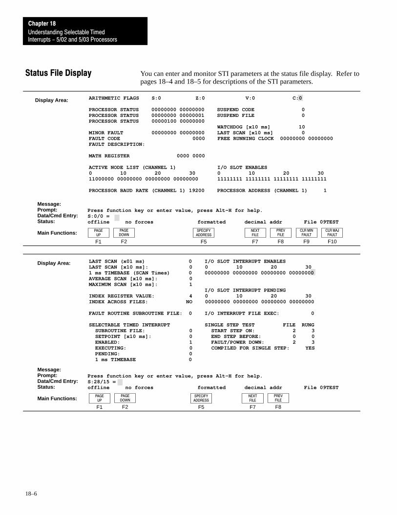
Interrupts - 5/02 and 5/03 Processors
Chapter 18
Understanding Selectable Timed
18–6
You can enter and monitor STI parameters at the status file display. Refer topages 18–4 and 18–5 for descriptions of the STI parameters.
ARITHMETIC FLAGS S:0 Z:0 V:0 C:0
PROCESSOR STATUS 00000000 00000000 SUSPEND CODE 0PROCESSOR STATUS 00000000 00000001 SUSPEND FILE 0PROCESSOR STATUS 00000100 00000000 WATCHDOG [x10 ms] 10MINOR FAULT 00000000 00000000 LAST SCAN [x10 ms] 0FAULT CODE 0000 FREE RUNNING CLOCK 00000000 00000000FAULT DESCRIPTION:
MATH REGISTER 0000 0000
ACTIVE NODE LIST (CHANNEL 1) I/O SLOT ENABLES0 10 20 30 0 10 20 3011000000 00000000 00000000 00000000 11111111 11111111 11111111 11111111
PROCESSOR BAUD RATE (CHANNEL 1) 19200 PROCESSOR ADDRESS (CHANNEL 1) 1
Press function key or enter value, press Alt–H for help.S:0/0 = offline no forces formatted decimal addr File 09TEST
Message:Prompt:Data/Cmd Entry:Status:
Main Functions:
F7F5
NEXTFILE
SPECIFYADDRESS
F9 F10F8
CLR MINFAULT
CLR MAJFAULT
PREVFILE
Display Area:
F1
PAGEUP
F2
PAGEDOWN
LAST SCAN (x01 ms) 0 I/O SLOT INTERRUPT ENABLESLAST SCAN [x10 ms]: 0 0 10 20 301 ms TIMEBASE (SCAN Times) 0 00000000 00000000 00000000 00000000AVERAGE SCAN [x10 ms]: 0 MAXIMUM SCAN [x10 ms]: 1
I/O SLOT INTERRUPT PENDINGINDEX REGISTER VALUE: 4 0 10 20 30INDEX ACROSS FILES: NO 00000000 00000000 00000000 00000000 FAULT ROUTINE SUBROUTINE FILE: 0 I/O INTERRUPT FILE EXEC: 0
SELECTABLE TIMED INTERRUPT SINGLE STEP TEST FILE RUNG SUBROUTINE FILE: 0 START STEP ON: 2 3 SETPOINT [x10 ms]: 0 END STEP BEFORE: 0 0 ENABLED: 1 FAULT/POWER DOWN: 2 3 EXECUTING: 0 COMPILED FOR SINGLE STEP: YES PENDING: 0 1 ms TIMEBASE 0
Display Area:
F7F5 F8
NEXTFILE
SPECIFYADDRESS
Press function key or enter value, press Alt–H for help.S:28/15 = offline no forces formatted decimal addr File 09TEST
Message:Prompt:Data/Cmd Entry:Status:
Main Functions:PREVFILE
F1 F2
PAGEUP
PAGEDOWN
Status File Display

Interrupts - 5/02 and 5/03 Processors
Chapter 18
Understanding Selectable Timed
18–7
The STD and STE instructions are used to create zones in which STIinterrupts cannot occur.
Selectable Timed Disable - STD
When true, this instruction resets the STI enable bit and prevents the STIsubroutine from executing. When the rung goes false, the STI enable bitremains reset until a true STS or STE instruction is executed. The STI timercontinues to operate while the enable bit is reset.
Selectable Timed Enable - STE
This instruction, upon a false-true transition of the rung, sets the STI enablebit and allows execution of the STI subroutine. When the rung goes false,the STI enable bit remains set until a true STD instruction is executed. Thisinstruction has no effect on the operation of the STI timer or setpoint. Whenthe enable bit is set, the first execution of the STI subroutine can occur at anyfraction of the timing cycle up to a full timing cycle later.
STD/STE Zone Example
In the program that follows, the STI function is in effect. The STD and STEinstructions in rungs 6 and 12 are included in the ladder program to avoidhaving STI subroutine execution at any point in rungs 7 through 11.
The STD instruction (rung 6) resets the STI enable bit and the STEinstruction (rung 12) sets the enable bit again. The STI timer increments andmay time out in the STD zone, setting the pending bit S:2/0 and overrun bitS:5/10.
The first pass bit S:1/15 and the STE instruction in rung 0 are included toinsure that the STI function is initialized following a power cycle. Youshould include this rung any time your program contains an STD/STE zoneor an STD instruction.
STDSELECTABLE TIMED DISABLE
STD and STE Instructions
STESELECTABLE TIMED ENABLE
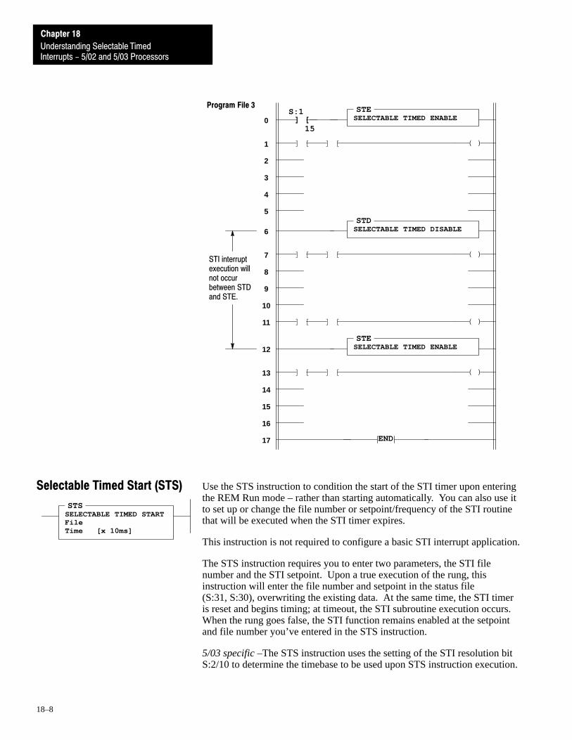
Interrupts - 5/02 and 5/03 Processors
Chapter 18
Understanding Selectable Timed
18–8
] [S:1
15
( )
STI interruptexecution willnot occurbetween STDand STE.
END
0
STDSELECTABLE TIMED DISABLE
STESELECTABLE TIMED ENABLE
] [ ] [
( )] [ ] [
( )] [ ] [
STESELECTABLE TIMED ENABLE
( )] [ ] [
1
2
3
4
5
6
7
8
9
10
11
12
13
14
15
16
17
Program File 3
Use the STS instruction to condition the start of the STI timer upon enteringthe REM Run mode – rather than starting automatically. You can also use itto set up or change the file number or setpoint/frequency of the STI routinethat will be executed when the STI timer expires.
This instruction is not required to configure a basic STI interrupt application.
The STS instruction requires you to enter two parameters, the STI filenumber and the STI setpoint. Upon a true execution of the rung, thisinstruction will enter the file number and setpoint in the status file(S:31, S:30), overwriting the existing data. At the same time, the STI timeris reset and begins timing; at timeout, the STI subroutine execution occurs.When the rung goes false, the STI function remains enabled at the setpointand file number you’ve entered in the STS instruction.
5/03 specific –The STS instruction uses the setting of the STI resolution bitS:2/10 to determine the timebase to be used upon STS instruction execution.
STSSELECTABLE TIMED STARTFileTime [x 10ms]
Selectable Timed Start (STS)
A–B 19Chapter
19–1
Understanding I/O Interrupts - 5/02 and 5/03 Processors
This chapter applies to the 5/02 and 5/03 processors only. It covers thefollowing topics:
• I/O operation• I/O interrupt parameters• IID and IIE instructions• RPI instruction• INT instruction
The I/O event-driven interrupt function is used with 5/02 and 5/03processors. This function allows a specialty I/O module to interrupt thenormal processor operating cycle in order to scan a specified subroutine file.Interrupt operation for a specific module is described in the user’s manual forthe module.
You cannot use a standard discrete I/O module to accomplish an I/Oevent–driven interrupt. Refer to chapter 17 in this manual for moreinformation about the discrete I/O interrupt.
Basic Programming Procedure for the I/O Interrupt Function
• Specialty I/O modules that create interrupts should be configured in thelowest numbered I/O slots. When you are configuring the specialty I/Omodule slot with the programming device, select the “SPIO CONFIG”function key and program the “ISR” (interrupt subroutine) program filenumber (range 3 to 255) that you want the I/O module to execute.Configuring I/O is discussed in chapter 7 in the Advanced ProgrammingSoftware User Manual, Catalog Number 1747–NM002.
• Create the subroutine file that you have specified in the I/O module slotconfiguration.Creating a subroutine file is discussed in chapter 8 in the AdvancedProgramming Software User Manual, Catalog Number 1747–NM002.
I/O Overview

5/02 and 5/03 Processors
Chapter 19
Understanding I/O Interrupts -
19–2
When you restore your program and enter the run mode, the I/O interruptbegins operation as follows:
1. The specialty I/O module determines that it needs servicing and generatesan interrupt request to the SLC processor.
2. The processor is interrupted from what it is doing, and the specifiedinterrupt subroutine file (ISR) is scanned.
3. When the ISR scan is completed, the specialty I/O module is notified.This informs the specialty I/O module that it is allowed to generate a newinterrupt.
4. The processor resumes normal operation from where it left off.
Interrupt Subroutine (ISR) Content
The Interrupt Subroutine (INT) instruction should be the first instruction inyour ISR. This identifies the subroutine file as an I/O interrupt subroutine.
The ISR contains the rungs of your application logic. You can program anyinstruction inside an ISR except a TND, REF, or SVC instruction. IIM orIOM instructions are needed in an ISR if your application requires immediateupdate of input or output points. Terminate the ISR with an RET (return)instruction.
JSR stack depth is limited to 3. That is, you may call other subroutines to alevel 3 deep from an ISR.
Interrupt Latency and Interrupt Occurrences
Interrupt latency is the interval between the I/O module’s request for serviceand the start of the interrupt subroutine. I/O interrupts can occur at any pointin your program, but not necessarily at the same point on successiveinterrupts. Interrupts can only occur between instructions in your program,inside the I/O scan (between slots), or between the servicing ofcommunication packets. The table below shows the interaction between aninterrupt and the processor operating cycle.
5/02 I/O Interrupts5/03 I/O Interrupts with
Bit S:33/8 set5/03 I/O Interrupts with
Bit S:33/8 cleared
Between slot updates Between word updates Between slot updates
Between instruction updates Between word updates Between rung updates
Between slot updates Between word updates Between slot updates
Between communicationpackets
Between word packet updatesBetween communicationpackets
At start and end Between word updates Between word upates
Operation
Processor Overhead
Communication
Output Scan
Program Scan
Input Scan
Events in the processor operating cycle

5/02 and 5/03 Processors
Chapter 19
Understanding I/O Interrupts -
19–3
Note that ISR execution time adds directly to the overall scan time. Duringthe latency period, the processor is performing operations that cannot bedisturbed by the STI interrupt function. Latency periods are:
• 5/02 series B processor interrupts are serviced within 3.7ms maximum.• 5/02 series C processor and later interrupts are serviced within 2.4ms
maximum.• 5/03 processor – If an interrupt occurs while the 5/03 processor is
performing a multi–word slot update and your interrupt subroutineaccesses that same slot, the multi–word transfer finishes to completionprior to performing the interrupt subroutine slot access. The 5/03Interrupt Latency Bit (S:33/8) functions as follows:– When the bit is set (1) interrupts are serviced within 500µs.– When the bit is clear (0), 500µs servicing is not expected. When
S:33/8 is clear (0), user interrupts occur between rungs and I/O slotupdates.
The default state is cleared (0). To determine the interrupt latency withS:33/8 clear, you must calculate the execution time of each and everyrung in your program. Refer to appendix B in the AdvancedProgramming Software User Manual, Catalog Number 1747–NM002 formore information on how to calculate the interrupt latency.
Interrupt Priorities
Interrupt priorities are as follows for 5/02 and 5/03 processors:
5/02 Processor 5/03 Processor
1. Fault Routine 1. Fault routine
2. STI Subroutine 2. Discrete Input Interrupt (DII)
3. I/O Interrupt Subroutine (ISR) 3. STI Subroutine
4. I/O Interrupt Subroutine (ISR)
An executing interrupt can only be interrupted by an interrupt having higherpriority.
The I/O interrupt cannot interrupt an executing fault routine, an executingDII subroutine, an executing STI subroutine, or another executing I/Ointerrupt subroutine. If an I/O interrupt occurs while the fault routine, DII, orSTI subroutine is executing, the processor waits until the higher priorityinterrupts are scanned to completion. The I/O interrupt subroutine is thenscanned.Important: 5/02 specific – It is important to understand that the I/O Pending
bit associated with the interrupting slot remains clear during thetime that the processor is waiting for the fault routine or STIsubroutine to finish.
Important: 5/03 specific – The I/O pending bit is always set when theinterrupt occurs. You can examine the state of these bits withinyour higher priority interrupt routines.

5/02 and 5/03 Processors
Chapter 19
Understanding I/O Interrupts -
19–4
If a major fault occurs while executing the I/O interrupt subroutine,execution immediately switches to the fault routine. If the fault wasrecovered by the fault routine, execution resumes at the point that it left offin the I/O interrupt subroutine. Otherwise, the fault mode is entered.
If a DII interrupt occurs while executing the I/O interrupt subroutine,execution immediately switches to the DII subroutine. When the DIIsubroutine is scanned to completion, execution resumes at the point that itleft off in the I/O interrupt subroutine.
If the STI timer expires while executing the I/O interrupt subroutine,execution will immediately switch to the STI subroutine. When the STIsubroutine is scanned to completion, execution resumes at the point that itleft off in the I/O interrupt subroutine.
If two or more I/O interrupt requests are detected by the processor at thesame instant, or while waiting for a higher or equal priority interruptsubroutine to finish, the interrupt subroutine associated with the specialty I/Omodule in the lowest slot number is scanned first. For example, if slot 2(ISR 20) and slot 3 (ISR 11) request interrupt service at the same instant, theprocessor first scans ISR 20 to completion, then ISR 11 to completion.
Status File Data Saved
Data in the following words is saved on entry to the I/O interrupt subroutineand re-written upon exiting the I/O interrupt subroutine.
• S:0 Arithmetic flags• S:13 and S:14 Math register• S:24 Index register

5/02 and 5/03 Processors
Chapter 19
Understanding I/O Interrupts -
19–5
The I/O interrupt parameters below have status file addresses. They aredescribed here and also in chapter 1 of this manual.
• S:11 and S:12 I/O Slot Enables – Read/Write. These words are bitmapped to the 30 I/O slots. Bits S:11/1 through S:12/14 refer to slots 1through 30. Bits S:11/0 and S:12/15 are reserved.The enable bit associated with an interrupting slot must be set when aninterrupt occurs. Otherwise a major fault will occur. Changes made tothese bits using the Data Monitor function take effect at the next end ofscan.
• S:25 and S:26 I/O Interrupt Pending Bits – Read only. These wordsare bit mapped to the 30 I/O slots. Bits S:25/1 through S:26/14 refer toslots 1 through 30. Bits S:25/0 and S:26/15 are reserved. The pending bitassociated with an interrupting slot is set when the corresponding I/O slotinterrupt enable bit is clear at the time of an interrupt request. It is clearedwhen the corresponding I/O event interrupt enable bit is set, or when anassociated RPI instruction is executed. The pending bit for an executingI/O interrupt subroutine remains clear when the ISR is interrupted by aDII, STI, or fault routine.5/02 specific – Likewise, the pending bit remains clear if interrupt serviceis requested at the time that a higher or equal priority interrupt isexecuting (fault routine, STI, or other ISR).5/03 specific – This bit is set if interrupt service is requested at the time ahigher or equal priority interrupt is executing (fault routine, DII, STI, orother ISR).
• S:27 and S:28 I/O Interrupt Enables – Read/Write. These words are bitmapped to the 30 I/O slots. Bits S:27/1 through S:28/14 refer to slots 1through 30. Bits S:27/0 and S:28/15 are reserved. The enable bitassociated with an interrupting slot must be set when the interrupt occursto allow the corresponding ISR to execute. Otherwise the ISR will notexecute and the associated I/O slot interrupt pending bit will be set.5/02 specific – Changes made to these bits using the data monitorfunction or ladder instruction take effect at the next end of scan.5/03 specific – Changes made to these bits using the data monitorfunction or ladder instruction take effect immediately.
• S:32 I/O Interrupt Executing Word – Read only. This word containsthe slot number of the specialty I/O module that generated the currentlyexecuting ISR. This value is cleared upon completion of the ISR, runmode entry, or upon power up. You can interrogate this word inside ofyour DII or STI subroutine or fault routine if you wish to know if thesehigher priority interrupts have interrupted an executing ISR. You mayalso use this value to discern interrupt slot identity when multiplexing twoor more specialty I/O module interrupts to the same ISR.
I/O Interrupt Parameters

5/02 and 5/03 Processors
Chapter 19
Understanding I/O Interrupts -
19–6
You can enter and monitor parameters at the status file displays of APSsoftware. Refer to page 19–5 for descriptions of the parameters.
ARITHMETIC FLAGS S:0 Z:0 V:0 C:0
PROCESSOR STATUS 00000000 00000000 SUSPEND CODE 0PROCESSOR STATUS 00000000 00000001 SUSPEND FILE 0PROCESSOR STATUS 00000000 00000000 WATCHDOG [x 10 ms] 10MINOR FAULT 00000000 00000000 LAST SCAN [x 10 ms] 0FAULT CODE 0000 FREE RUNNING CLOCK 00000000 00000000FAULT DESCRIPTION:
MATH REGISTER 0000 0000
ACTIVE NODE LIST (CHANNEL 1) I/O SLOT ENABLES0 10 20 30 0 10 20 3011000000 00000000 00000000 00000000 11111111 11111111 11111111 11111111
PROCESSOR BAUD RATE (CHANNEL 1) 19200 PROCESSOR ADDRESS (CHANNEL 1) 1
Press function key or enter value, press Alt–H for help.S:0/0 = offline no forces formatted decimal addr File 09TEST
Message:Prompt:Data/Cmd Entry:Status:
Main Functions:
F7F5
NEXTFILE
SPECIFYADDRESS
F9 F10F8
CLR MINFAULT
CLR MAJFAULT
PREVFILE
Display Area:
F1
PAGEUP
F2
PAGEDOWN
LAST SCAN (x01 ms) 0 I/O SLOT INTERRUPT ENABLESLAST SCAN [x10 ms]: 0 0 10 20 301 ms TIMEBASE (SCAN Times) 0 00000000 00000000 00000000 00000000AVERAGE SCAN [x10 ms]: 0 MAXIMUM SCAN [x10 ms]: 1
I/O SLOT INTERRUPT PENDINGINDEX REGISTER VALUE: 4 0 10 20 30INDEX ACROSS FILES: NO 00000000 00000000 00000000 00000000 FAULT ROUTINE SUBROUTINE FILE: 0 I/O INTERRUPT FILE EXEC: 0
SELECTABLE TIMED INTERRUPT SINGLE STEP TEST FILE RUNG SUBROUTINE FILE: 0 START STEP ON: 2 3 SETPOINT [x10 ms]: 0 END STEP BEFORE: 0 0 ENABLED: 1 FAULT/POWER DOWN: 2 3 EXECUTING: 0 COMPILED FOR SINGLE STEP: YES PENDING: 0 1 ms TIMEBASE 0
Display Area:
F7F5 F8
NEXTFILE
SPECIFYADDRESS
Press function key or enter value, press Alt–H for help.S:28/15 = offline no forces formatted decimal addr File 09TEST
Message:Prompt:Data/Cmd Entry:Status:
Main Functions:PREVFILE
F1 F2
PAGEUP
PAGEDOWN
Status File Display
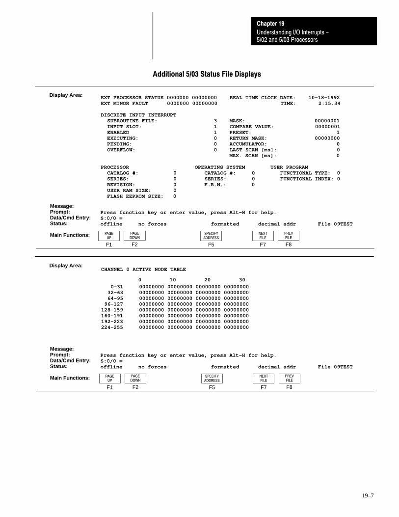
5/02 and 5/03 Processors
Chapter 19
Understanding I/O Interrupts -
19–7
Additional 5/03 Status File Displays
EXT PROCESSOR STATUS 0000000 00000000 REAL TIME CLOCK DATE: 10–18–1992EXT MINOR FAULT 0000000 00000000 TIME: 2:15.34
DISCRETE INPUT INTERRUPT SUBROUTINE FILE: 3 MASK: 00000001 INPUT SLOT: 1 COMPARE VALUE: 00000001 ENABLED 1 PRESET: 1 EXECUTING: 0 RETURN MASK: 00000000 PENDING: 0 ACCUMULATOR: 0 OVERFLOW: 0 LAST SCAN [ms]: 0
MAX. SCAN [ms]: 0
PROCESSOR OPERATING SYSTEM USER PROGRAM CATALOG #: 0 CATALOG #: 0 FUNCTIONAL TYPE: 0 SERIES: 0 SERIES: 0 FUNCTIONAL INDEX: 0 REVISION: 0 F.R.N.: 0 USER RAM SIZE: 0 FLASH EEPROM SIZE: 0
Display Area:
Press function key or enter value, press Alt–H for help.S:0/0 = offline no forces formatted decimal addr File 09TEST
Message:Prompt:Data/Cmd Entry:Status:
Main Functions:
F7F5 F8
NEXTFILE
SPECIFYADDRESS
PREVFILE
F1 F2
PAGEUP
PAGEDOWN
CHANNEL 0 ACTIVE NODE TABLE
0–31 00000000 00000000 00000000 00000000 32–63 00000000 00000000 00000000 00000000 64–95 00000000 00000000 00000000 00000000 96–127 00000000 00000000 00000000 00000000128–159 00000000 00000000 00000000 00000000160–191 00000000 00000000 00000000 O0000000192–223 00000000 00000000 00000000 00000000224–255 00000000 00000000 00000000 00000000
Display Area:
0 10 20 30
Press function key or enter value, press Alt–H for help.S:0/0 = offline no forces formatted decimal addr File 09TEST
Message:Prompt:Data/Cmd Entry:Status:
Main Functions:
F7F5 F8
NEXTFILE
SPECIFYADDRESS
PREVFILE
F1 F2
PAGEUP
PAGEDOWN

5/02 and 5/03 Processors
Chapter 19
Understanding I/O Interrupts -
19–8
Use the I/O Interrupt Disable (IID) and I/O Interrupt Enable (IIE)instructions to create zones in which I/O interrupts cannot occur.
I/O Interrupt Disable - IID
Use this instruction together with an IIE instruction to create a zone in yourmain ladder program file or subroutine file in which I/O interrupts cannotoccur. The IID instruction takes effect immediately upon execution.5/02 specific – Setting/clearing the I/O interrupt enable bits (S:27 and S:28)with a programming device or standard instruction such as MVM takes effectat the END of the scan only.5/03 specific – Setting/clearing the I/O interrupt enable bits (S:27 and S:28)with a programming device or standard instruction such as MVM takes effectimmediately.
When true, this instruction clears the I/O interrupt enable bits (S:27/1through S:28/14) corresponding to the slots parameter of the instruction(slots 1, 2, 7 in the example above). Interrupt subroutines of the affectedslots will not be able to execute when an interrupt request is made. Instead,the corresponding I/O pending bits (S:25/1 through S:26/14) will be set. TheISR will not be executed until an IIE instruction with the same slot parameteris executed, or until the end of the scan during which you use a programmingdevice to set the corresponding status file bit.
I/O Interrupt Enable - IIE
Use this instruction together with the IID instruction to create a zone in yourmain ladder program file or subroutine file in which I/O interrupts cannotoccur. The IIE instruction takes effect immediately upon execution.5/03 specific – Setting/clearing the I/O interrupt enable bits (S:27 and S:28)with a programming device or standard instruction such as MVM takes effectimmediately.
When true, this instruction sets the I/O interrupt enable bits (S:27/1 throughS:28/14) corresponding to the slots parameter of the instruction (slots 1, 2, 7in the example above). Interrupt subroutines of the affected slots will regainthe ability to execute when an interrupt request is made. If an interrupt waspending (S:25/1 through S:26/14) and the pending slot corresponds to the IIEslots parameter, the ISR associated with that slot will execute immediately.
I/O Interrupt Disable (IID) andI/O Interrupt Enable (IIE)
IIDI/O INTERRUPT DISABLESlots: 1,2,7
IIEI/O INTERRUPT ENABLESlots: 1,2,7

5/02 and 5/03 Processors
Chapter 19
Understanding I/O Interrupts -
19–9
IID/IIE Zone Example
In the program below, slots 1, 2, and 7 are capable of generating I/Ointerrupts. The IID and IIE instructions in rungs 6 and 12 are included toavoid having I/O interrupt ISRs execute as a result of interrupt requests fromslots 1, 2, or 7. This allows rungs 7 through 11 to execute withoutinterruption.
] [S:1
15
( )
ISR executionwill not occurbetween IID
and IIEinstructions.
END
0
] [ ] [
( )] [ ] [
( )] [ ] [
( )] [ ] [
1
2
3
4
5
6
7
8
9
10
11
12
13
14
15
16
17
Program File 2
IIDI/O INTERRUPT DISABLESlots: 1,2,7
IIEI/O INTERRUPT ENABLESlots: 1,2,7
IIEI/O INTERRUPT ENABLESlots: 1,2,7
The first pass bit S:1/15 and the IIE instruction in rung 0are included to insure that the I/O interrupt function isinitialized following a power cycle. You should include arung such as this any time your program contains anIID/IIE zone or an IID instruction.
The IID instruction in rung 6 clears the I/O interruptenable bits associated with slots 1, 2, and 7 (S:27/1,S:27/2, and S:27/7). The IIE instruction in rung 12 setsthese same bits. If an I/O interrupt is detected by theprocessor while the processor is executing rungs 7-11,the interrupt will be marked as pending. (S:25/1,S:25/2, and/or S:25/7 will be set.) All interrupts markedas pending will be serviced upon execution of rung 12.The lowest numbered slot is serviced first when multiplepending bits are set.

5/02 and 5/03 Processors
Chapter 19
Understanding I/O Interrupts -
19–10
Use the RPI instruction to purge unwanted I/O interrupt requests. Thisinstruction is not required to configure a basic I/O interrupt application.
When true, this instruction clears the I/O pending bits (S:25/1 throughS:26/14) corresponding to the slots parameter of the instruction. In addition,the processor notifies the specialty I/O modules in those slots that theirinterrupt request was aborted. Following this notice, the slot may once againrequest interrupt service. This instruction does not affect the I/O slotinterrupt enable bits (S:27/1 through S:28/14).
Use the INT instruction in I/O event-driven interrupt subroutines (ISRs) andSTIs for identification purposes. Use of this instruction is optional.
This instruction has no control bits and is always evaluated as true. Whenused, the INT should be programmed as the first instruction of the first rungof the ISR.
Reset Pending Interrupt (RPI)
RPIRESET PENDING INTERRUPTSlots: 1–30
Interrupt Subroutine (INT)INT
INTERRUPT SUBROUTINE
A–B AAppendix
A–1
Number Systems
This appendix:
• describes the different number system you need to understand for use ofAPS and the SLC 500 family controllers
• covers binary and hexadecimal numbers• explains the use of a hex mask to filter data in certain programming
instructions
The SLC 500 processor performs almost all calculations on signed integervalues. Most operands used to perform these calculations are sized at 16bits. A signed 16 bit integer spans the range of –32,768 to 32,767. These 16bit values can be displayed or entered in several radicies. The radicies thatrlogin can be displayed using the APS programming software are:
• Integer• Binary• ASCII• Hexadecimal
When entering values into an APS instruction or data table element, you canspecify the radix of your entry using the “&” special operator. The radiciesthat can be used to enter data into an APS instruction or data table elementare:
• Integer (&N)• Binary (&B)• ASCII (&A)• Hexadecimal (&H)• BCD (&D)• Octal (&O)
The data type you select when programming an APS instruction determinesthe display radix. For example, if a 16–bit value contains the value 48decimal:
• an N: type element is displayed as 48• a B: type element is displayed as 0000000000110000• a Hexadecimal radix is displayed as 0030• an ASCII radix is displayed as 100 0
You may enter or display a value in several radicies, however, the processorwill always operate on the data in the format described for the particularinstruction. Using the above example, an ADD instruction would always add48 decimal, regardless of the radix used to enter or display this value.Likewise, the Mask parameter of a MVM instruction would use the value0030.
Radices Used in APS
Appendix A
Number Systems
A–2
Example
You are prompted to enter the second parameter of an EQU instruction andyou wish to enter a constant. Constants are displayed in the Integer radix.Using the value 48, this value can be entered using any one of the followingmethods:
• &H0030 (&H specifies the hexadecimal radix)• &B0000000000110000 (&B specifies the binary radix)• &O60 (&O specifies the octal radix)• &A0 (&A specifies the ASCII radix)• &D0048 (&D specifies the BCD radix)• &N48 (&N specifies the Integer radix)
In this case, &N is not required because the Integer is the default radix forconstants. You would enter 48.
The processor memory stores 16-bit binary numbers. As indicated in thefigure below, each position in the number has a decimal value, beginning atthe right with 20 and ending at the left with 215.
Each position can be 0 or 1 in the processor memory. A 0 indicates a valueof 0; a 1 indicates the decimal value of the position. The equivalent decimalvalue of the binary number is the sum of the position values.
Positive Decimal Values
The far left position will always be 0 for positive values. As indicated in thefigure, this limits the maximum positive decimal value to 32767. Allpositions are 1 except the far left position.
Other examples:
0000 1001 0000 1110 = 211+28+23+22+21
= 2048+256+8+4+2 = 2318
0010 0011 0010 1000 = 213+29+28+25+23
= 8192+512+256+32+8
= 9000
Binary Numbers
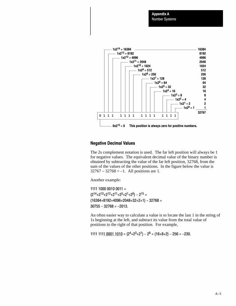
Appendix A
Number Systems
A–3
1x214 = 16384
1x213 = 8192
1x212 = 4096
1x211 = 2048
1x210 = 1024
1x29 = 512
1x28 = 256
1x27 = 128
1x26 = 64
1x25 = 32
1x24 = 16
1x23 = 8
1x22 = 4
1x21 = 2
1x20 = 1
10 1 1 11 1 1 11 1 1 11 1 1
16384
8192
4096
2048
1024
512
256
128
64
32
16
8
4
2
1
32767
0x215 = 0 This position is always zero for positive numbers.
Negative Decimal Values
The 2s complement notation is used. The far left position will always be 1for negative values. The equivalent decimal value of the binary number isobtained by subtracting the value of the far left position, 32768, from thesum of the values of the other positions. In the figure below the value is32767 – 32768 = –1. All positions are 1.
Another example:
1111 1000 0010 0011 =
(214+213+212+211+25+21+20) - 215 =
(16384+8192+4096+2048+32+2+1) - 32768 =
30755 - 32768 = -2013.
An often easier way to calculate a value is to locate the last 1 in the string of1s beginning at the left, and subtract its value from the total value ofpositions to the right of that position. For example,
1111 1111 0001 1010 = (24+23+21) - 28 = (16+8+2) - 256 = -230.

Appendix A
Number Systems
A–4
1x214 = 16384
1x213 = 8192
1x212 = 4096
1x211 = 2048
1x210 = 1024
1x29 = 512
1x28 = 256
1x27 = 128
1x26 = 64
1x25 = 32
1x24 = 16
1x23 = 8
1x22 = 4
1x21 = 2
1x20 = 1
11 1 1 11 1 1 11 1 1 11 1 1
16384
8192
4096
2048
1024
512
256
128
64
32
16
8
4
2
1
32767
1x215 = 32768 This position is always 1 for negative numbers.
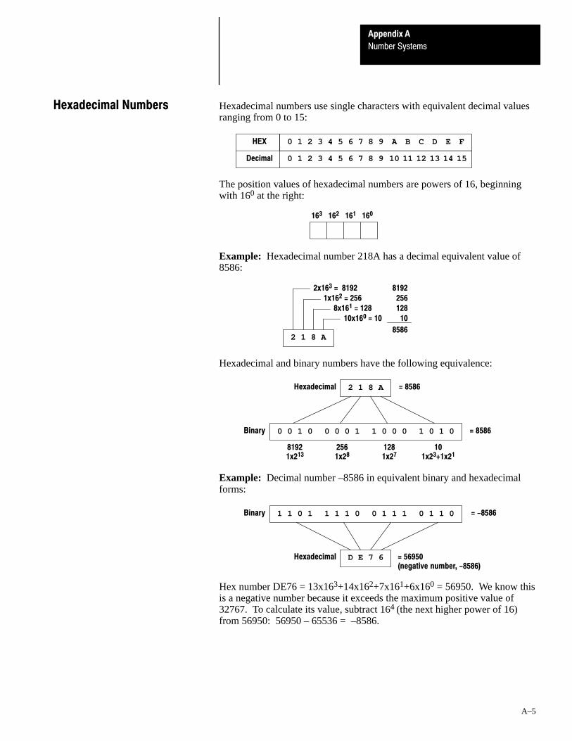
Appendix A
Number Systems
A–5
Hexadecimal numbers use single characters with equivalent decimal valuesranging from 0 to 15:
10 2 3 54 6 7 98 A B DC E F
10 2 3 54 6 7 98 10 11 1312 14 15
HEX
Decimal
The position values of hexadecimal numbers are powers of 16, beginningwith 160 at the right:
163 162 161 160
Example: Hexadecimal number 218A has a decimal equivalent value of8586:
12 8 A
10x160 = 10
8x161 = 128
1x162 = 256
2x163 = 8192
10
128
256
8192
8586
Hexadecimal and binary numbers have the following equivalence:
12 8 A
00 1 0 00 0 1 01 0 0 01 1 0
81921x213
2561x28
1281x27
101x23+1x21
Binary = 8586
Hexadecimal = 8586
Example: Decimal number –8586 in equivalent binary and hexadecimalforms:
11 0 1 11 1 0 10 1 1 10 1 0Binary = -8586
ED 7 6Hexadecimal = 56950(negative number, -8586)
Hex number DE76 = 13x163+14x162+7x161+6x160 = 56950. We know thisis a negative number because it exceeds the maximum positive value of32767. To calculate its value, subtract 164 (the next higher power of 16)from 56950: 56950 – 65536 = –8586.
Hexadecimal Numbers

Appendix A
Number Systems
A–6
This is a 4-character code, entered as a parameter in SQO, SQC, and otherinstructions to exclude selected bits of a word from being operated on by theinstruction. The hex values are used in their binary equivalent form, asindicated in the figure below. The figure also shows an example of a hexcode and the corresponding mask word.
00 F F
00 0 0 00 0 0 11 1 1 11 1 1
Hex Code
Mask Word
HexValue
0123456789ABCDEF
BinaryValue
0000000100100011010001010110011110001001101010111100110111101111
Bits of the mask word that are set (1) will pass data from a source to adestination. Reset bits (0) will not. In the example below, data in bits 0–7 ofthe source word is passed to the destination word. Data in bits 8–15 of thesource word is not passed to the destination word.
11 1 0 01 0 1 11 0 0 01 1 0Source Word
00 0 0 00 0 0 11 1 1 11 1 1Mask Word
00 0 0 00 0 0 11 0 0 01 1 0Destination Word(all bits 0 initially)
Hex Mask
A–B BAppendix
B–1
APS Error Messages
This appendix contains APS error messages, which can occur duringoperation.
Often, APS errors are caused due to incorrect configuration of your personalcomputer. Verify that your system is configured as follows:
• CONFIG.SYS file should be set as: FILES=30; BUFFERS=30.
• Extended/expanded memory manager must be LIM 3.2 or higher.
APS runs with most Terminate and Stay Resident (TSR) programs.However, some TSR programs causes APS to operate erratically. Therefore,we recommend that no TSR programs execute while APS is running. If youchoose to forego this recommendation and you experience difficulties, editand mark out your TSR’s one by one until you find the offensive TSR. Thisalso applies to device drivers (other than extended/expanded memorymanagers).
Display Message Description Recommended Action
ADDRESS OUT OF RANGEThe specified device you aretrying to communicate with isout of memory.
Check the device and yourcommand; retry the function
ALL REQUIRED OPERANDS HAVE NOTBEEN ENTERED
While programming aninstruction an operand(s) wasleft out.
Enter all operands and retrythe function.
ATTEMPTING TO RESTORE FILE TOPROCESSOR, PROCESSOR MUST BE INPROGRAM MODE
During a restore, or whenattempting switching fromoffline editing to onlinemonitoring, the offline programwas not downloaded becausethe processor was not inprogram mode.
Place the processor in programmode and retry the function.
BAD REPLACE STRINGThe text entered for a replacestring does not have thecorrect syntax.
Check the syntax and correct ifnecessary. Retry the function.
BAD SEARCH STRINGThe text entered for a searchstring does not have thecorrect syntax.
Check the syntax and correct ifnecessary. Retry the function.
BOTH SOURCE OPERANDS CANNOT BECONSTANTS
Source A and Source Boperands are both constants.
Change one of the operands toan address. Retry the function.
BRIDGE DEVICE NO LONGERRESPONDING
While online with DF1 FullDuplex through a KF3 (with orwithout a modem) adisconnection or hangupoccurred.
Retry the function.
General Information

APS Error Messages
Appendix B
B–2
Display Message Description Recommended Action
BRIDGE DEVICE NOT ACTIVEInability to attach to a KF3while going online with DF1Full Duplex.
Retry the function.
CANNOT INSERT A RUNG BETWEEN ANIR PAIR
An attempt was made to insert,append, or undelete a rungbetween an inserted markedrung followed by a replacedmarked rung.
Move the cursor before or afterthe IR pair and try to insert,append, or undelete the nextrung.
CANNOT MODIFY DATA TABLE SIZEDURING ONLINE EDITING
Modification of data table sizesor creation of new data tablescannot occur while in an onlineediting session.
Go offline to change the datatable sizes and retry thefunction.
CANNOT MODIFY PARAMETER VIA 5/03PROCESSOR'S CHANNEL 0
An attempt to change a node'sowner, the max. address, nodeaddress, or baud rate of a 5/03while it was communicatingwith APS over channel 0 wasmade.
Not allowed.
CANNOT MODIFY PROTECTED DATA FILEDURING ONLINE EDITING
During an online editingsession, an attempt was madeto modify data tables that wereconstantly protected.
Not allowed. Go offline to eitherchange the data file protectionand retry the function, or editthe program offline.
CAUTION: REMOVING OUTPUTREFERENCES LEAVES THE OUTPUTS INTHEIR LAST STATE
Either 1) the Test Edits functionkey was pressed and edits doexist in the ladder program; or2) an attempt to delete aninstruction was made.
Be aware that changes mayresult to the output states whenthe new assembled editsbecome active or when arestore is performed via quickedits.
CAUTION: VERIFY STATE OF OUTPUTSWITH DATA MONITOR
You directed APS to assembleall existing online edits or aquick edit program.
Be aware that changes mayresult to the output states whenthe new assembled editsbecome active or when arestore is performed via quickedits.
CHANNEL CONFIGURATION MAY CAUSELOSS OF COMMUNICATIONS
Applies only if you are online.An incompatibility existsbetween the 5/03 and thecurrent online configuration(APS).
Check your onlineconfiguration and retry thefunction.
CHANNEL CONFIGURATION NOTAVAILABLE FOR SELECTED PROCESSOR
A processor other than a 5/03is selected.
Verify that a 5/03 processor isselected. Retry the function.
CHANNEL CONFIGURATION MODIFIED,ACCEPT OR UNDO CHANGES
The [ESC] or [ALT-U] keywas pressed after a changewas selected.
Informational message. Noaction necessary.
CHANNEL CONFIGURATION MAY CAUSELOSS OF COMMUNICATIONS
Online only - An incompatibilitybetween the 5/03 and thecurrent online (APS)configuration exists.
Verify that the selected onlineconfiguration is compatible witha 5/03. Retry the function.
COMMAND CANNOT BE EXECUTED
This message could mean 1)you are not the program owner;or 2) the file is in use byanother device.
Determine why another nodehas explicit access.
APS Error MessagesAppendix B
B–3
Display Message Description Recommended Action
COMMENT DATA LOSTThe text storage capacity of arung, address, or instructioncomment has been exceeded.
Install a memory module,change mode, or install forces.
CONDITION CANNOT BE GENERATED
This message indicates either1) no memory module exists;2) the processor is in faultmode; or 3) no forces areinstalled.
Informational message. Noaction necessary.
CONVERSION SUCCESSFUL-BYTESCONVERTED
An archive file wassuccessfully converted into ahex file.
Send the hex file to a promprogrammer.
CREATION OF XREF DB ENTRY FAILED
While attempting to create thecross reference databaseduring create reports, adatabase call generated anerror.
Contact your A-Brepresentative.
DATA FILES CAN ONLY BE PROTECTEDFOR 5/03 PROCESSOR TYPES
An attempt to modify programprotection for a non 5/03processor occurred.
Change the processor to a5/03 and retry the function.
DATABASE READ ERRORA DOS file read error occurredor a program documentationfile was altered.
Check your CONFIG.SYS filefor proper set up. (FILES=30and BUFFERS=30.) Verify thatno TSR programs areinterferring with APS. Ifchanges are made, you mustreboot the computer.
DATABASE WRITE ERROR A DOS file write error occurred.
Check your CONFIG.SYS filefor proper set up. (FILES=30and BUFFERS=30). Verify thatno TSR programs areinterferring with APS. Ifchanges are made, you mustreboot the computer.
DECOMPILER BAD MATRIXDECOMPILER CRC ERROR
A decompiler error occurred.The message always beginswith �DECOMPILER."
Contact your A-Brepresentative.
DESTINATION DIRECTORY CANNOT BETHE SAME AS A SOURCE DIRECTORY
The copy to/from directoriesare the same.
Change one of the directoriesand retry the function.
DESTINATION DIRECTORY MUST BESPECIFIED
During copy to, the destinationdirectory was not specified.
Specify the destinationdirectory and retry the function.
DOWNLOAD ABORTED
During quick edits, when tryingto switch from offline editing toonline monitoring, Ctrl-C waspressed during the downloadphase.
The offline ladder editor isdisplayed.
DUPLICATE NODE ADDRESSTwo or more devices on thenetwork have the sameaddress.
Change the Terminal Addressin On-line Configuration. Retrythis function.

APS Error Messages
Appendix B
B–4
Display Message Description Recommended Action
ENQ RETRIES EXHAUSTEDDF1 Full Duplex is not getting aresponse from the KF3.
Check for electrical noiseproblem on network wiring andretry the function.
CREATION OF XREF DB ENTRY FAILED
While attempting to create thecross reference databaseduring create reports, adatabase call generated anerror.
Contact your A-Brepresentative.
DATA FILES CAN ONLY BE PROTECTEDFOR 5/03 PROCESSOR TYPES
An attempt to modify programprotection for a non 5/03processor occurred.
Change the processor to a5/03 and retry the function.
DATABASE READ ERRORA DOS file read error occurredor a program documentationfile was altered.
Check your CONFIG.SYS filefor proper set up. (FILES=30and BUFFERS=30). Verify thatno TSR programs areinterferring with APS. Ifchanges are made, you mustreboot the computer.
DATABASE WRITE ERROR A DOS file write error occurred.
Check your CONFIG.SYS filefor proper set up. (FILES=30and BUFFERS=30). Verify thatno TSR programs areinterferring with APS. Ifchanges are made, you mustreboot the computer.
DECOMPILER BAD MATRIXDECOMPILER CRC ERROR
A decompiler error occurred.The message always beginswith �DECOMPILER."
Contact your A-Brepresentative.
DESTINATION DIRECTORY CANNOT BETHE SAME AS A SOURCE DIRECTORY
The copy to/from directoriesare the same.
Change one of the directoriesand retry the function.
DESTINATION DIRECTORY MUST BESPECIFIED
During copy to, the destinationdirectory was not specified.
Specify the destinationdirectory and retry the function.
DOWNLOAD ABORTED
During quick edits, when tryingto switch from offline editing toonline monitoring, Ctrl-C waspressed during the downloadphase.
The offline ladder editor isdisplayed.
DUPLICATE NODE ADDRESSTwo or more devices on thenetwork have the sameaddress.
Change the Terminal Addressin On-line Configuration. Retrythis function.
ENQ RETRIES EXHAUSTEDDF1 Full Duplex is not getting aresponse from the KF3.
Check for electrical noiseproblem on network wiring andretry the function.
ERROR ACCESSING PROCESSOR I/OCONFIGURATION FILE
Attempt to read the I/O autoconfiguration file from thespecified 5/03 processor failed.
Retry the function.

APS Error MessagesAppendix B
B–5
Display Message Description Recommened Action
ERROR - ALLOCATING SPACE
To convert the processor imageto a hex file, the softwarerequests space from thesystem. Insufficient spacegenerated an error.
At the DOS prompt verify thatat least 580K of memory exists.Remove any TSRs that may betaking memory space. Retrythe function.
ERROR - CLOSING ARCHIVE FILEWhile attempting to close anarchive file an error occurred.
Check your disk space byrunning �CHKDSK" from yourDOS prompt. On successfulcompletion retry the function.
ERROR - CLOSING HEX FILEWhile attempting to close a hexfile an error occurred.
Check your disk space byrunning �CHKDSK" from yourDOS prompt. On successfulcompletion retry the function.
ERROR - NOT ENOUGH MEMORY TOACCEPT CURRENT RUNG
Transfer of an accepted rung toa 5/03 failed because there isnot enough program space forthe selected rung size in theprocessor.
Reduce or optimize your userprogram or perform offlineediting.
ERROR - OPENING ARCHIVE FILEWhile attempting to open anarchive file an error occurred.
Check your disk space byrunning �CHKDSK" from yourDOS prompt. On successfulcompletion retry the function.
ERROR - OPENING HEX FILEWhile attempting to open ahex file an error occurred.
Check your disk space byrunning �CHKDSK" from yourDOS prompt. On successfulcompletion retry the function.
ERROR - READING HEADER OF ARCHIVEFILE
While reading the header in thearchive file an error occurred.
Check your disk space byrunning �CHKDSK" from yourDOS prompt. On successfulcompletion retry the function.
ERROR - READING PROCESSOR IMAGEFILE STRUCTURE
While reading the processorimage in the archive file anerror occurred.
Check your disk space byrunning �CHKDSK" from yourDOS prompt. On successfulcompletion retry the function.
ERROR - READING PROCESSOR IMAGEFROM ARCHIVE FILE
While reading the processorimage in the archive file anerror occurred.
Check your disk space byrunning �CHKDSK" from yourDOS prompt. On successfulcompletion retry the function.
ERROR - READING PROCESSOR STATICSTRUCTURE
While reading the processorimage in the archive file anerror occurred.
Check your disk space byrunning �CHKDSK" from yourDOS prompt. On successfulcompletion retry the function.
ERROR - REFINDING PROCESSOR IMAGEWhile reading the processorimage in the archive file anerror occurred.
Check your disk space byrunning �CHKDSK" from yourDOS prompt. On successfulcompletion retry the function.
ERROR - SPECIFIED LADDER FILE DOESNOT EXIST
During create program listing,when specifying the file/rungrange, the specified ladder filedid not exist.
Specify a different file numberor create a file and retry thefunction.

APS Error Messages
Appendix B
B–6
Display Message Description Recommended Action
ERROR - SPECIFIED RUNG DOES NOTEXIST IN SPECIFIED FILE
During create program listing,the specified rung number didnot exist.
Specify a different rung numberor create a rung and retry thefunction.
ERROR - TOO FEW DATA FILES IN THISARCHIVE FILE
An error occurred whileaccessing data files.
Contact your A-Brepresentative.
ERROR - UNABLE TO CALCULATE PROMSIZE
The processor image is invalid.Resave the file and retry thefunction.
ERROR - UNABLE TO FIND PROCESSORIMAGE
While reading the processorimage in the archive file anerror occurred.
Check your disk space byrunning �CHKDSK" from yourDOS prompt. Retry thefunction.
ERROR - WRITING DATA RECORDThe software is unable to writeto the current hex file.
Check your disk space byrunning �CHKDSK" from yourDOS prompt. On successfulcompletion retry the function.
ERROR - WRITING END OF FILE RECORDThe software is unable to writeto the current hex file.
Check your disk space byrunning �CHKDSK" from yourDOS prompt. On successfulcompletion retry the function.
ERROR - WRITING LRC RECORDThe software is unable to writeto the current hex file.
Check your disk space byrunning �CHKDSK" from yourDOS prompt. On successfulcompletion retry the function.
ERROR CLOSING REPORT LISTING FILEDuring create reports anattempt to close a report listingfailed.
Verify that the path(ipds\lis\slc500) exists and thatthe file is not write protected.
ERROR COPYING FILESThe routine called to copy filesfailed.
Check your disk space byrunning �CHKDSK" from yourDOS prompt. On successfulcompletion retry the function.
ERROR CREATING NEW ARCHIVE FILEAn error occurred while savingthe file contents to disk.
Check your disk space byrunning �CHKDSK" from yourDOS prompt. On successfulcompletion retry the function.
ERROR DELETING FILESThe routine called to deletefiles failed.
Check your disk space byrunning �CHKDSK" from yourDOS prompt. On successfulcompletion retry the function.
ERROR GETTING DIRECTORY LISTAn error occurred when thedirectory list of files was beingretrieved by APS.
Check your disk space byrunning �CHKDSK" from yourDOS prompt. On successfulcompletion retry the function.
ERROR INITIALIZING COMMUNICATIONSDRIVER
The communication driverspecified by the current onlineconfiguration could not beloaded or initialized.
Save your key strokes andprogram that created this error.Contact your A-Brepresentative.

APS Error MessagesAppendix B
B–7
Display Message Description Recommended Action
ERROR MAPPING LADDER FILE RUNG
During create reports an erroroccurred while attempting tomap rung or address/instruction comments tocorresponding rungs,addresses, or instructions.
Contact your A-Brepresentative.
ERROR OPENING COMMUNICATIONPROTOCOL FILE
Either a disk read erroroccurred or the driver file doesnot exist in the specifieddirectory.
Verify that the driver file existsand execute �CHKDSK" fromthe DOS prompt. Retry thefunction.
ERROR OPENING REPORT LISTING FILEDuring create reports anattempt to close a report listingfailed.
Verify that the DOS pathcontains (ipds\lis\slc500) andthat the file is not writeprotected.
ERROR POSITIONING PROCESSOR FILEPOINTER
During create reports anattempt to set a file pointer to aladder executable file in thearchive file failed.
Contact your A-Brepresentative.
ERROR READINGADDRESS/INSTRUCTION COMMENTFROM DATABASE
During create reports an erroroccurred while attempting toread an address/instructioncomment from the commentsdatabase.
Check your disk space byrunning �CHKDSK" from yourDOS prompt. On successfulcompletion retry the function.
ERROR READING COMMUNICATIONPROTOCOL FILE
An error occurred while tryingto start the comms. driver.
Verify that the driver file existsand execute �CHKDSK" fromthe DOS prompt. Retry thefunction.
ERROR READING LADDER FILE RUNGDuring create reports anattempt to read a rung from thedatabase failed.
Check your disk space byrunning �CHKDSK" from yourDOS prompt. On successfulcompletion retry the function.
ERROR READING RUNG COMMENT FROMDATABASE
During create reports an erroroccurred while attempting toread a rung comment from therung comments database.
Check your disk space byrunning �CHKDSK" from yourDOS prompt. On successfulcompletion retry the function.
ERROR RENAMING FILESThe routine called to renamefiles failed.
Check your disk space byrunning �CHKDSK" from yourDOS prompt. On successfulcompletion retry the function.
ERROR RENAMING REPORT LISTING FILEDuring create reports anattempt to rename a reportlisting failed.
Verify that the DOS pathcontains (ipds\lis\slc500) andthat the file is not writeprotected.
ERROR WRITING CONFIGURATION FILEThe configuration file was notsuccessfully saved to the userpreference file.
Check the configuration fileand save the file.
ERROR WRITING TO REPORT LISTINGFILE
During create reports anattempt to write to a reportlisting failed.
Verify that the DOS path(ipds\lis\slc500) exists and thatthe file is not write protected.
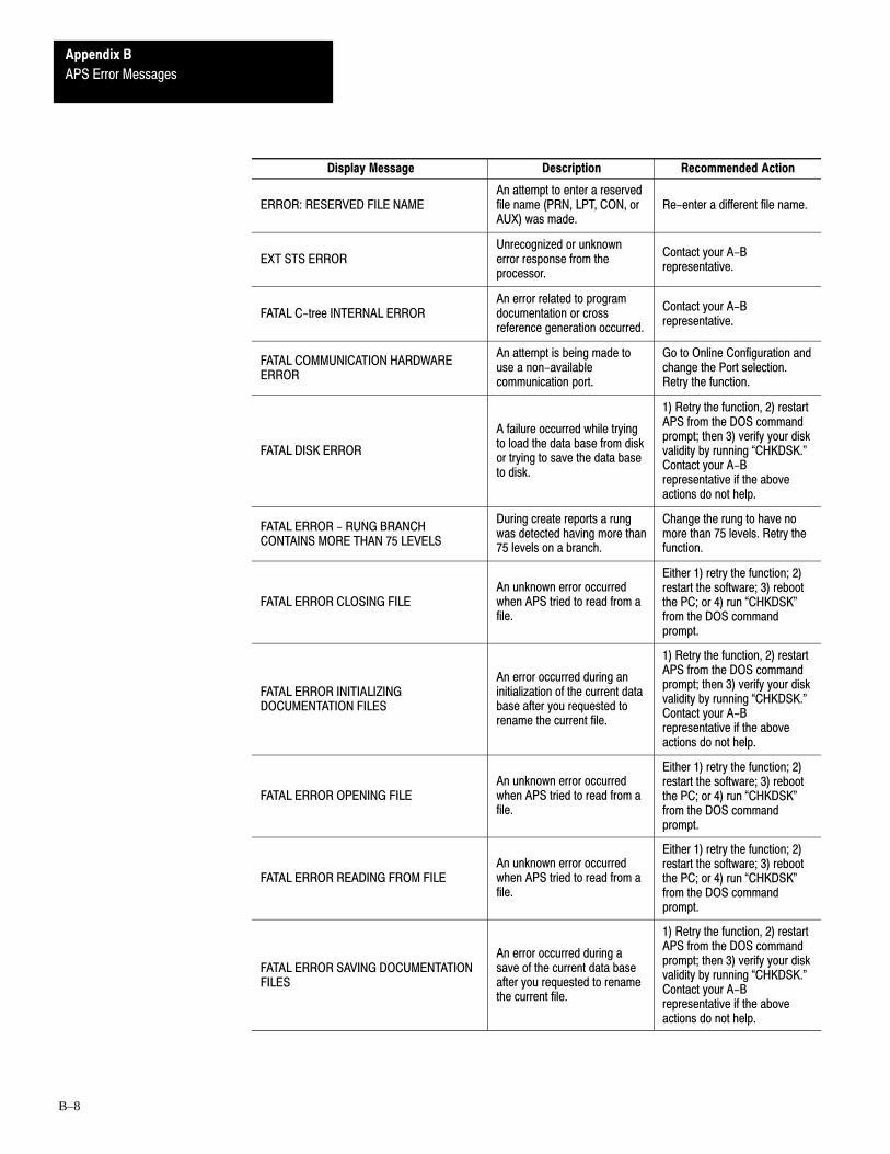
APS Error Messages
Appendix B
B–8
Display Message Description Recommended Action
ERROR: RESERVED FILE NAMEAn attempt to enter a reservedfile name (PRN, LPT, CON, orAUX) was made.
Re-enter a different file name.
EXT STS ERRORUnrecognized or unknownerror response from theprocessor.
Contact your A-Brepresentative.
FATAL C-tree INTERNAL ERRORAn error related to programdocumentation or crossreference generation occurred.
Contact your A-Brepresentative.
FATAL COMMUNICATION HARDWAREERROR
An attempt is being made touse a non-availablecommunication port.
Go to Online Configuration andchange the Port selection.Retry the function.
FATAL DISK ERROR
A failure occurred while tryingto load the data base from diskor trying to save the data baseto disk.
1) Retry the function, 2) restartAPS from the DOS commandprompt; then 3) verify your diskvalidity by running �CHKDSK."Contact your A-Brepresentative if the aboveactions do not help.
FATAL ERROR - RUNG BRANCHCONTAINS MORE THAN 75 LEVELS
During create reports a rungwas detected having more than75 levels on a branch.
Change the rung to have nomore than 75 levels. Retry thefunction.
FATAL ERROR CLOSING FILEAn unknown error occurredwhen APS tried to read from afile.
Either 1) retry the function; 2)restart the software; 3) rebootthe PC; or 4) run �CHKDSK"from the DOS commandprompt.
FATAL ERROR INITIALIZINGDOCUMENTATION FILES
An error occurred during aninitialization of the current database after you requested torename the current file.
1) Retry the function, 2) restartAPS from the DOS commandprompt; then 3) verify your diskvalidity by running �CHKDSK."Contact your A-Brepresentative if the aboveactions do not help.
FATAL ERROR OPENING FILEAn unknown error occurredwhen APS tried to read from afile.
Either 1) retry the function; 2)restart the software; 3) rebootthe PC; or 4) run �CHKDSK"from the DOS commandprompt.
FATAL ERROR READING FROM FILEAn unknown error occurredwhen APS tried to read from afile.
Either 1) retry the function; 2)restart the software; 3) rebootthe PC; or 4) run �CHKDSK"from the DOS commandprompt.
FATAL ERROR SAVING DOCUMENTATIONFILES
An error occurred during asave of the current data baseafter you requested to renamethe current file.
1) Retry the function, 2) restartAPS from the DOS commandprompt; then 3) verify your diskvalidity by running �CHKDSK."Contact your A-Brepresentative if the aboveactions do not help.

APS Error MessagesAppendix B
B–9
Display Message Description Recommended Action
FATAL ERROR WRITING TO FILEAn unknown error occurredwhen APS tried to write from afile.
Either 1) retry the function; 2)restart the software; 3) rebootthe PC; or 4) run �CHKDSK"from the DOS commandprompt.
FATAL INTERNAL ERROR
Either 1) APS was not able toallocate memory from DOSwhile you were reviewing/editing comments or symbols;or 2) APS was initializing andcould not allocate DOSmemory for internal datastorage.
Verify your disk validity byrunning �CHKDSK" from theDOS command prompt. Werecommend 525Kbytesavailable for APS 3.01 and550Kbytes available forAPS 4.0.
FATAL INTERNAL MANAGE FILES ERRORA fatal error occurred in the MFfunction.
Either 1) retry the function; 2)restart the software; 3) rebootthe PC; or 4) run �CHKDSK"from the DOS commandprompt.
FATAL MEMORY ERRORAn error occurred whilerequesting space from thesystem.
Either 1) retry the function; 2)restart the software; 3) rebootthe PC; or 4) run �CHKDSK"from the DOS commandprompt.
FILE, RUNG, INSTRUCTION FILEOVERWRITE ERROR
For instruction types thatcontain file addresses and acorresponding length,adequate data table spacemust exist for the file addressplus a number of addressespast that address. During aprogram save or test edits aninstruction was detected thatviolates this rule.
Change the file address orlength and retry the function.
FILE, RUNG, INSTRUCTION, I/O ADDRESSUNDEFINED
During a program save or testedits, an input or outputaddress has been detected ona rung but the address is notconfigured for the givenprocessor.
Change the address or I/Oconfiguration and retry thefunction.
FILE, RUNG, INSTRUCTION, M0/M1ADDRESS NOT CONFIGURED
During a program save or testedits, an M0/M1 address hasbeen detected on a rung butthe address is not configuredfor the given processor.
Change the address or I/Oconfiguration and retry thefunction.
FILE, RUNG, END MCR IS ONLYALLOWABLE INSTRUCTION ON RUNG
Rungs containing `end MCR'cannot contain any otherinstructions on that rung.During a program save or testedits a rung was detected thatviolates this rule.
Configure the address for thegiven processor and resave theprogram.
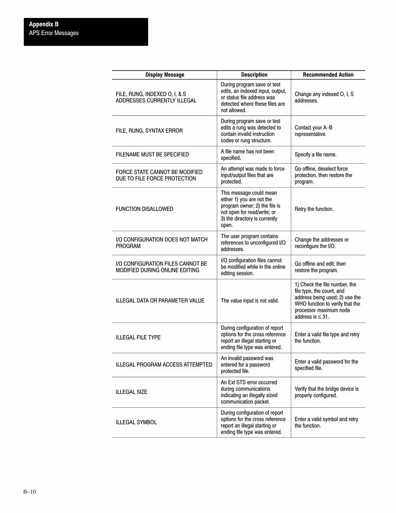
APS Error Messages
Appendix B
B–10
Display Message Description Recommended Action
FILE, RUNG, INDEXED O, I, & SADDRESSES CURRENTLY ILLEGAL
During program save or testedits, an indexed input, output,or status file address wasdetected where these files arenot allowed.
Change any indexed O, I, Saddresses.
FILE, RUNG, SYNTAX ERROR
During program save or testedits a rung was detected tocontain invalid instructioncodes or rung structure.
Contact your A-Brepresentative.
FILENAME MUST BE SPECIFIEDA file name has not beenspecified.
Specify a file name.
FORCE STATE CANNOT BE MODIFIEDDUE TO FILE FORCE PROTECTION
An attempt was made to forceinput/output files that areprotected.
Go offline, deselect forceprotection, then restore theprogram.
FUNCTION DISALLOWED
This message could meaneither 1) you are not theprogram owner; 2) the file isnot open for read/write; or3) the directory is currentlyopen.
Retry the function.
I/O CONFIGURATION DOES NOT MATCHPROGRAM
The user program containsreferences to unconfigured I/Oaddresses.
Change the addresses orreconfigure the I/O.
I/O CONFIGURATION FILES CANNOT BEMODIFIED DURING ONLINE EDITING
I/O configuration files cannotbe modified while in the onlineediting session.
Go offline and edit; thenrestore the program.
ILLEGAL DATA OR PARAMETER VALUE The value input is not valid.
1) Check the file number, thefile type, the count, andaddress being used; 2) use theWHO function to verify that theprocessor maximum nodeaddress is ≤ 31.
ILLEGAL FILE TYPE
During configuration of reportoptions for the cross referencereport an illegal starting orending file type was entered.
Enter a valid file type and retrythe function.
ILLEGAL PROGRAM ACCESS ATTEMPTEDAn invalid password wasentered for a passwordprotected file.
Enter a valid password for thespecified file.
ILLEGAL SIZE
An Ext STS error occurredduring communicationsindicating an illegally sizedcommunication packet.
Verify that the bridge device isproperly configured.
ILLEGAL SYMBOL
During configuration of reportoptions for the cross referencereport an illegal starting orending file type was entered.
Enter a valid symbol and retrythe function.

APS Error MessagesAppendix B
B–11
Display Message Description Recommended Action
INCOMPATIBLE DEVICEThe version of the software isunable to communicate withthe requested device.
Contact your A-Brepresentative.
INPUT INVALID, PLEASE REENTER Incorrect syntax entered. Retry the function.
INPUT, OUTPUT, AND STATUS FILESCANNOT BE CONSTANT PROTECTED
An attempt to constant protectthese types of files was made.
Apply only static protection tothese types of files.
INSTRUCTION HAS NO OPERANDS`Modify symbol' was selected,but the instruction does nothave any operands.
Informational message. Noaction necessary.
INSTRUCTION HAS NO OPERANDS TORELATE TO SYMBOL
The instruction has operands,but none of the operandssupport a symbol name.
Re-enter the user instructionaddress.
INTEGRITY CHECK OF SERIAL NUMBERHAS FAILED, REINSTALL SOFTWAREPACKAGE
The runtime CRC does notmatch the install-time CRC.APS aborts because the serialnumber has been tamperedwith.
Reinstall the software.
INVALID BOARD ADDRESSAn illegal board address wasentered.
Enter a valid board addressand retry the function.
INVALID G-FILE SIZEAn attempt was made to setthe G-File size greater than256 words.
Set the G-File size to no morethan 256 words.
INVALID ISR FILE NUMBERAn attempt was made to set anISR number to the reserved ormain ladder program files.
Verify the destination of theISR number. Valid ISRnumbers are 0, 4-255.
INVALID M0 FILE SIZEAn attempt was made to entera numeric value that can bestored as the M0 file size.
Retry the function.
INVALID M1 FILE SIZEAn attempt was made to entera numeric value that can bestored as the M1 file size.
Retry the function.
INVALID CHARAn illegal character wasentered in a file name.
Verify that entered charactersare valid. Valid characters are:A-Z, a-z, 0-9, OR `_'. Retrythe function.
INVALID COMMANDA key was pressed that APSwas not expecting.
Retry the function.
INVALID COMMUNICATION DRIVER FILEFORMAT
An error occurred while tryingto start the communicationdriver.
Verify that the driver file existsand execute �CHKDSK" fromthe DOS prompt. Retry thefunction.
INVALID FILE NUMBER
During program save or testedits and error occurred whileattempting to copy a data tablefrom the database to theprocessor image.
Retry the function. If you stillhave problems contact yourA-B representative.

APS Error Messages
Appendix B
B–12
Display Message Description Recommended Action
INVALID FILE TYPE
The instruction does not permitthe use of the entered file typeor the file number is alreadydefined as a different type offile.
Specify a valid file type andretry the function.
INVALID MODULE INPUT/OUTPUT SIZE
An attempt was made to setthe input or output size greaterthan 32 words for a singlemodule.
Set the input or output size tono more than 32 words for asingle module.
INVALID OPERANDIncorrect syntax was enteredfor the operand.
Enter a valid operand and retrythe function.
KF3 ADDRESS CANNOT EQUALPROCESSOR ADDRESS
The 1770-KF3 and processorare at the same node address.
Change their node addressesto be unique.
LINK ERRORUnrecognized or unknownproblem with thecommunication driver.
Retry the function. If you stillhave problems contact yourA-B representative.
LOSS OF MODEM CARRIER
While online with DF1 FullDuplex through a 1770-KF3and a modem, a disconnectionor hangup occurred.
Retry the function.
LOSS OF MODEM DSR STATUSWhile online with DF1 FullDuplex through a 1770-KF3,the modem went inactive.
Check the connection and retrythe function.
M0/M1 ADDRESS MONITORING ONLYSUPPORTED ONLINE
An attempt to monitor anM0/M1 file was made using aprocessor other than a 5/03.
Change the processor to a5/03; and go online with APS;retry M0/M1 addressmonitoring.
M0/M1 ADDRESS MONITORINGCURRENTLY DISABLED
M0/M1 address monitoring isdisabled in the APSconfiguration.
Enable M0/M1 addressmonitoring and retry thefunction.
M0/M1 ADDRESSES CANNOT BEMODIFIED
Unable to modify M0/M1addresses from the M0/M1data table monitor.
Informational message. Youcannot modify M0 and M1 filesfrom the data table monitor.
MAXIMUM COMMUNICATION DRIVER SIZEEXCEEDED
The link layer driver is to largeto fit into the memory available.
Verify the size, date, and timefor the link layer file. Also run�CHKDSK" from the DOSprompt.
MAXIMUM NODE ADDRESS VIOLATIONDETECTED
The software detected a deviceat a node higher than thecurrent maximum nodeaddress.
Change the Max. NodeAddress in the onlineConfiguration screen.
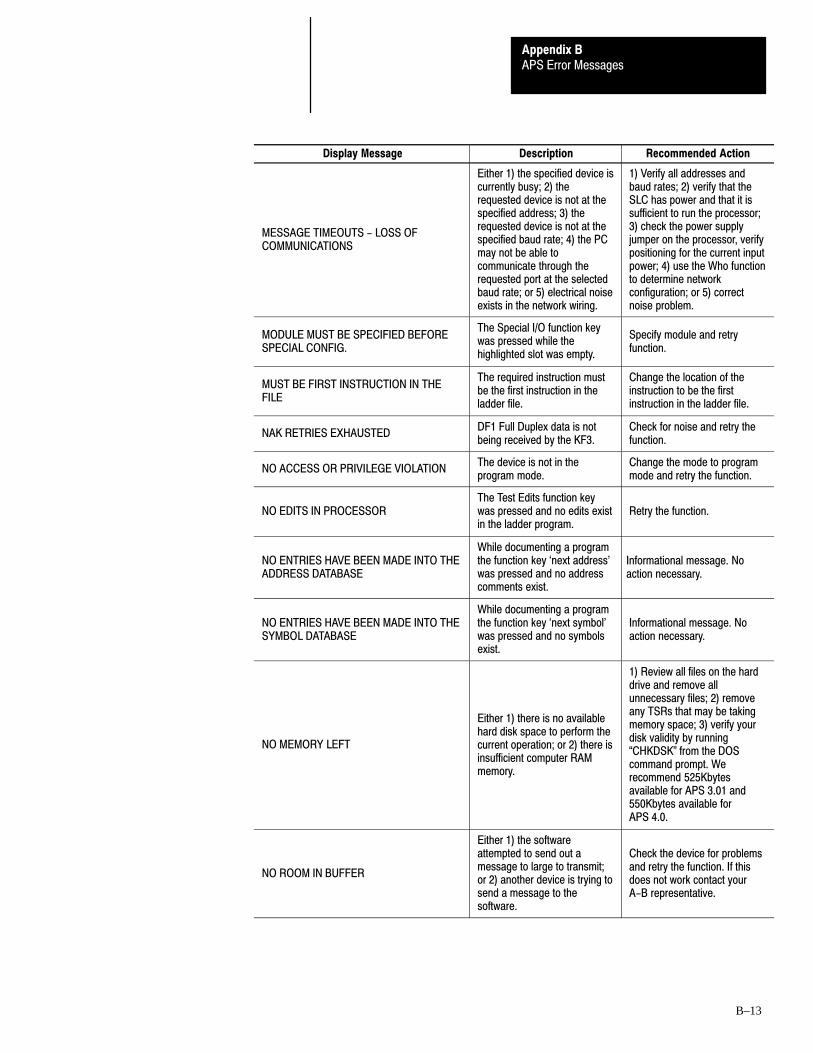
APS Error MessagesAppendix B
B–13
Display Message Description Recommended Action
MESSAGE TIMEOUTS - LOSS OFCOMMUNICATIONS
Either 1) the specified device iscurrently busy; 2) therequested device is not at thespecified address; 3) therequested device is not at thespecified baud rate; 4) the PCmay not be able tocommunicate through therequested port at the selectedbaud rate; or 5) electrical noiseexists in the network wiring.
1) Verify all addresses andbaud rates; 2) verify that theSLC has power and that it issufficient to run the processor;3) check the power supplyjumper on the processor, verifypositioning for the current inputpower; 4) use the Who functionto determine networkconfiguration; or 5) correctnoise problem.
MODULE MUST BE SPECIFIED BEFORESPECIAL CONFIG.
The Special I/O function keywas pressed while thehighlighted slot was empty.
Specify module and retryfunction.
MUST BE FIRST INSTRUCTION IN THEFILE
The required instruction mustbe the first instruction in theladder file.
Change the location of theinstruction to be the firstinstruction in the ladder file.
NAK RETRIES EXHAUSTEDDF1 Full Duplex data is notbeing received by the KF3.
Check for noise and retry thefunction.
NO ACCESS OR PRIVILEGE VIOLATIONThe device is not in theprogram mode.
Change the mode to programmode and retry the function.
NO EDITS IN PROCESSORThe Test Edits function keywas pressed and no edits existin the ladder program.
Retry the function.
NO ENTRIES HAVE BEEN MADE INTO THEADDRESS DATABASE
While documenting a programthe function key `next address'was pressed and no addresscomments exist.
Informational message. Noaction necessary.
NO ENTRIES HAVE BEEN MADE INTO THESYMBOL DATABASE
While documenting a programthe function key `next symbol'was pressed and no symbolsexist.
Informational message. Noaction necessary.
NO MEMORY LEFT
Either 1) there is no availablehard disk space to perform thecurrent operation; or 2) there isinsufficient computer RAMmemory.
1) Review all files on the harddrive and remove allunnecessary files; 2) removeany TSRs that may be takingmemory space; 3) verify yourdisk validity by running�CHKDSK" from the DOScommand prompt. Werecommend 525Kbytesavailable for APS 3.01 and550Kbytes available forAPS 4.0.
NO ROOM IN BUFFER
Either 1) the softwareattempted to send out amessage to large to transmit;or 2) another device is trying tosend a message to thesoftware.
Check the device for problemsand retry the function. If thisdoes not work contact yourA-B representative.

APS Error Messages
Appendix B
B–14
Display Message Description Recommended Action
NO SPACE FOR TAB INSERT HEREThe text storage for a rung,address, or instructioncomment has been exceeded.
Informational message. Noaction necessary.
NO SYMBOL TO REMOVEInvalid symbol name wasentered.
Enter a valid symbol name.
NOT A LADDER FILE
An attempt to jump to a ladderfile was made, but the filenumber specified is not aladder file.
Verify the operation and specifya valid ladder file.
NOT ENOUGH MEMORY FORCOMMUNICATION DRIVER
The software package tried toload files that exceeded128KBytes.
Retry the function and ifnecessary exit and restart thesoftware. If the error continuesvalidate the disk by running the�CHKDSK" from the DOSprompt.
ONLINE EDITING NOT AVAILABLE, INVALIDKEYSWITCH POSITION
Online editing is not allowedwhen the 5/03 keyswitch is inthe Run position.
Change the keyswitch to theRemote or Program position.Retry the function.
PROCESSOR MEMORY CORRUPTEDThe processor's memory iscurrently invalid.
Clear the processor memoryand retry the function.
OPERAND MUST BE INDEXEDThe operand for the currentinstruction is not indexed.
Index the operand and retry thefunction.
OPERATOR ABORTED DIALUP
While going online with DF1Full Duplex through a1770-KF3 and a modem the[ESC] key was pressed.
Retry the function.
OUT OF DATA TABLE MEMORY
During program save or testedits an error occurred whileattempting to copy a data tablefrom the database to theprocessor image.
The program is too large.Reduce the program memoryrequirements.
OUT OF MEMORY IN PROCESSOR IMAGE
Either 1) during program saveor test edits all availablememory in the processorimage was used by theprogram; or 2) the program istoo big for the processor.
The program is too large.Reduce the program memoryrequirements.
OUT OF MEMORY IN PROGRAMMINGDEVICE
During program save or testedits all available memory inthe programming device wasused.
The program is too large.Reduce the program memoryrequirements.
PARSE ERROREntry on line was an invalid fileor rung number.
Verify file or rung entry andretry the function.
PLINK ErrorsThese errors indicate softwarepackage problems.
Attempt to reinstall APS andcall your A-B representative.
PROCESSOR DATA VALUES MAY HAVECHANGED
During quick edits, whenswitching from offline to onlinemonitoring, the offline datatables were downloaded.
Changes to the processor datatables may occur if the offlinedata tables do not match theonline data tables. Verify forthe correct data tables.
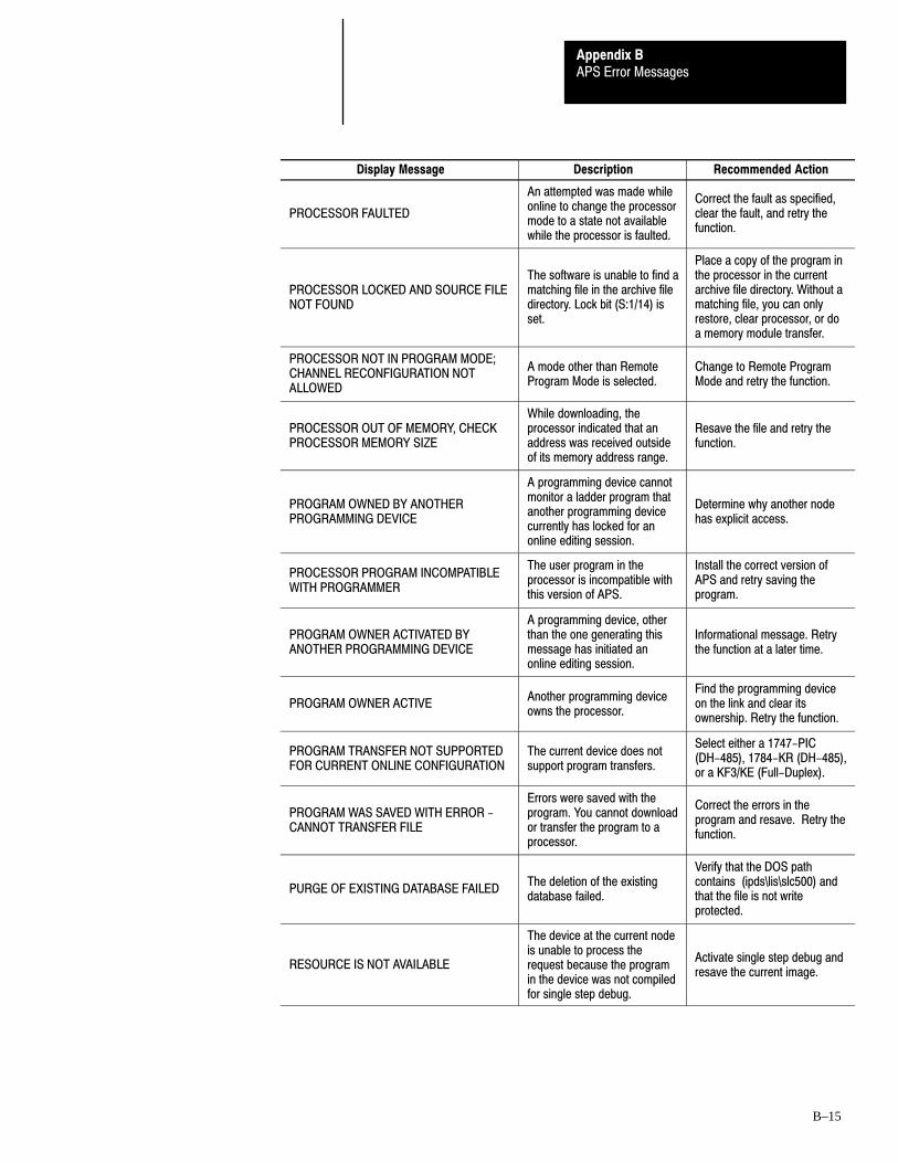
APS Error MessagesAppendix B
B–15
Display Message Description Recommended Action
PROCESSOR FAULTED
An attempted was made whileonline to change the processormode to a state not availablewhile the processor is faulted.
Correct the fault as specified,clear the fault, and retry thefunction.
PROCESSOR LOCKED AND SOURCE FILENOT FOUND
The software is unable to find amatching file in the archive filedirectory. Lock bit (S:1/14) isset.
Place a copy of the program inthe processor in the currentarchive file directory. Without amatching file, you can onlyrestore, clear processor, or doa memory module transfer.
PROCESSOR NOT IN PROGRAM MODE;CHANNEL RECONFIGURATION NOTALLOWED
A mode other than RemoteProgram Mode is selected.
Change to Remote ProgramMode and retry the function.
PROCESSOR OUT OF MEMORY, CHECKPROCESSOR MEMORY SIZE
While downloading, theprocessor indicated that anaddress was received outsideof its memory address range.
Resave the file and retry thefunction.
PROGRAM OWNED BY ANOTHERPROGRAMMING DEVICE
A programming device cannotmonitor a ladder program thatanother programming devicecurrently has locked for anonline editing session.
Determine why another nodehas explicit access.
PROCESSOR PROGRAM INCOMPATIBLEWITH PROGRAMMER
The user program in theprocessor is incompatible withthis version of APS.
Install the correct version ofAPS and retry saving theprogram.
PROGRAM OWNER ACTIVATED BYANOTHER PROGRAMMING DEVICE
A programming device, otherthan the one generating thismessage has initiated anonline editing session.
Informational message. Retrythe function at a later time.
PROGRAM OWNER ACTIVEAnother programming deviceowns the processor.
Find the programming deviceon the link and clear itsownership. Retry the function.
PROGRAM TRANSFER NOT SUPPORTEDFOR CURRENT ONLINE CONFIGURATION
The current device does notsupport program transfers.
Select either a 1747-PIC(DH-485), 1784-KR (DH-485),or a KF3/KE (Full-Duplex).
PROGRAM WAS SAVED WITH ERROR -CANNOT TRANSFER FILE
Errors were saved with theprogram. You cannot downloador transfer the program to aprocessor.
Correct the errors in theprogram and resave. Retry thefunction.
PURGE OF EXISTING DATABASE FAILEDThe deletion of the existingdatabase failed.
Verify that the DOS pathcontains (ipds\lis\slc500) andthat the file is not writeprotected.
RESOURCE IS NOT AVAILABLE
The device at the current nodeis unable to process therequest because the programin the device was not compiledfor single step debug.
Activate single step debug andresave the current image.

APS Error Messages
Appendix B
B–16
Display Message Description Recommended Action
SAME ADDRESS FOUND, ONLY ADDRESSCURRENTLY IN DATABASE
While documenting a programfunction key �next address"was pressed and only oneaddress comment exists.
Informational message. Noaction necessary.
SAME SYMBOL FOUND, ONLY SYMBOLCURRENTLY IN DATABASE
While documenting a programfunction key �next symbol" waspressed and only one symbolexists.
Informational message. Noaction necessary.
SCANNED I/O IS TOO LARGE
A scanned I/O value wasentered which exceeded theactual Input or Output imagesize for the selected module.
Change to a valid size andretry the function.
SEARCH FOR OPERAND FAILED
During create reports an erroroccurred while attempting tosearch the cross referencedatabase.
Check your disk space byrunning �CHKDSK" from yourDOS prompt. On successfulcompletion retry the function.
SEARCH FOR XREF OCCURRENCEFAILED
During create reports an erroroccurred while attempting tosearch for an existing crossreference database entry.
Check your disk space byrunning �CHKDSK" from yourDOS prompt. On successfulcompletion retry the function.
SEARCH OF DOCUMENTATION DB FAILED
During create reports an erroroccurred while attempting tosearch the cross referencedatabase.
Check your disk space byrunning �CHKDSK" from yourDOS prompt. On successfulcompletion retry the function.
SELECTED PROCESSOR DOES NOTSUPPORT THIS FEATURE
I/O auto configuration is notavailable for the currentprocessor.
Change the processor to a5/03 and retry the function.
SOFTWARE NOT INSTALLED PROPERLYThe personalization dataentered during the installationprocess is missing.
Reinstall the software.
SOURCE DIRECTORY CANNOT BE THESAME AS THE DESTINATION DIRECTORY
The copy to/from the paths arethe same.
Change one of the paths andretry the function.
STARTING FILE TYPE MUST BE BEFOREENDING FILE TYPE
During configuration of reportoptions a starting file type thatis alphabetically after theending file type has beenentered.
Change the file types and retrythe function.
STARTING SYMBOL MUST BE BEFORESYMBOL
During configuration of reportoptions a starting file type thatis alphabetically after theending symbol has beenentered.
Change the symbols and retrythe function.
STATION NOT GETTING SOLICITED
Valid traffic is being detectedon the network, but thesoftware is unable to receivethe traffic.
Go to online configuration andchange the Terminal Addressto a lower address.
STS LOCAL ERRORUnrecognized or unknownerror response from theprocessor.
Retry the function.

APS Error MessagesAppendix B
B–17
Display Message Description Recommended Action
STS REMOTE ERRORUnrecognized or unknownerror response from theprocessor.
Retry the function.
TERMINAL ADDRESS CANNOT EQUALKA5 ADDRESS
The 1785-KA5 and terminalare at the same node address.
Change their node addressesto be unique.
TEXT EDITOR EXIT FORCED; NO MOREADDRESSES EXIST IN DATABASE
While documenting a programfunction key �next comment"was pressed.
Retry the function.
TEXT EDITOR EXIT FORCED; NO MORESYMBOLS EXIST IN DATABASE
While documenting a programfunction key �next comment"was pressed.
Retry the function.
THIS FIELD CANNOT BE CHANGED WHENAUTO IS SELECTED
An attempt to change a PIDvalue in a field is being madewhile in AUTO mode.
Change the mode selection toMANUAL by pressing [F8],Data Monitor. This can be doneoffline or online.
TOO MANY INSTRUCTIONS ON A RUNG
During program save or testedits a rung has been detectedwhich contains more than 128instructions.
Change the rung to contain nomore than 128 instructions.
UNABLE TO ACCESS USER CONFIG DIRUSING DEFAULT DIRECTORY
The specified userconfiguration directory does notexist.
Use the default directory( \ipds\attach\slc500).
UNABLE TO CONVERT ARCHIVE FILE -CORRUPTED PROCESSOR IMAGE
The processor image is invalid.Resave the file and retry thefunction.
UNABLE TO CONVERT ARCHIVE FILE -DEVICE SIZE REQUESTED TOO SMALL
The software cannot translatethe archive file because theprocessor image will not fit intothe requested PROM.
Select an alternate prom sizeand retry the function.
UNABLE TO CONVERT ARCHIVE FILE -INVALID PROCESSOR IMAGE SAVED
The processor image is invalid.Resave the file and retry thefunction.
UNABLE TO CONVERT ARCHIVE FILE -NO PROCESSOR IMAGE
The processor image is invalid.Resave the file and retry thefunction.
UNABLE TO CREATE/DELETE PROGRAMFILE DURING ONLINE EDITING
Program file creation ordeletion is not allowed duringan online editing session.
Go offline to create/deleteprogram files.
UNABLE TO SUCCESSFULLY READARCHIVE FILE
While reading the processorimage in the archive file afailure occurred.
Verify your disk validity byrunning �CHKDSK" from theDOS command prompt. Onsuccessful completion retry thefunction.
UNMATCHED MCRSDuring program save or testedits an unpaired MCRinstruction was detected.
Verify that all MCRs occur inpairs. Retry the function.
USER PROGRAM INCOMPATIBLE WITHPROCESSOR OPERATING SYSTEM
The current user program isincompatible with the selectedprocessor.
Change the processor andattempt to restore the userprogram again.

APS Error Messages
Appendix B
B–18
Display Message Description Recommended Action
WARNING: INSTRUCTION PROVIDES NOFUNCTION; BOTH CHANNELS AREDISABLED
For a SVC and REF using a5/03 both channels areprogrammed as disabled.
Informational message. Noaction necessary.
WHO NOT SUPPORTED FOR CURRENTONLINE CONFIGURATION
Who Active and Who Listenare not supported by thecurrent online configuration.
Informational message. Noaction necessary.

A
access denied bit (S:1/14), 1-10
active nodes (S:9 and S:10), 1-25
Add (ADD), 8-3math instruction, 8-3
Allen-Bradley, P-4contacting for assistance, P-4
And (AND), 9-4logical instruction, 9-4
APS error messages, B-1
arithmetic flags (S:0), 1-4
average scan time (S:23), 1-31
B
battery low bit (S:5/11), 1-18
baud rate (S:15H), 1-28
bit instructionsExamine if Closed (XIC), 3-1Examine if Open (XIO), 3-2One-Shot Rising (OSR), 3-4Output Energize (OTE), 3-2Output Latch (OTL), 3-3Output Unlatch (OTU), 3-3
bit shift instructions, 11-1Bit Shift Left (BSL), 11-2
operation, 11-3Bit Shift Right (BSR), 11-2
operation, 11-3
Bit Shift Left (BSL), 11-2bit shift instruction, 11-2
Bit Shift Right (BSR), 11-2bit shift instruction, 11-2
C
carry bit (S:0/0), 1-4
channel 0 active nodes (S:67 to S:83), 1-40
channel 0 modem lost (S:5/14), 1-19
Clear (CLR), 8-8math instruction, 8-8
clock/calendar day (S:39), 1-37
clock/calendar hours (S:40), 1-38
clock/calendar minutes (S:41), 1-38
clock/calendar month (S:38), 1-37
clock/calendar seconds (S:42), 1-38
clock/calendar year (S:37), 1-37
common interface file addressing mode(S:2/8), 1-12
communication instructions, 5-1error codes, 5-30message instruction (5/02 only), 5-1
application examples, 5-9configuration options, 5-2
local read/write to a 485 CIF (PLC2emulation), 5-2
local read/write to another SLC 500processor, 5-2
control block layout, 5-8, 5-29entering parameters, 5-3timing diagram, 5-6using status bits, 5-5
message instruction (5/03 only), 5-13configuration options, 5-14
local read/write to a 485CIF, 5-14, 5-18
local read/write to another SLC 500processor, 5-14, 5-16
remote read/write to a 485CIF, 5-14, 5-20
remote read/write to a 485CIF(PLC2 emulation), 5-14, 5-23
control block layout, 5-29entering parameters, 5-14illustration of remote messaging,
5-25related status file bits, 5-13timing diagram, 5-26using status bits, 5-15
communications active (channel 0) (S:33/4), 1-34
communications active bit (S:1/7), 1-5
communications servicing selection(channel 0) (S:33/5), 1-34
comparison instructions, 7-1Equal (EQU), 7-1Greater Than (GRT), 7-2Greater Than or Equal (GEQ), 7-3Less Than or Equal (LEQ), 7-2Less Then (LES), 7-2Limit Test (LIM), 7-3Masked Comparison for Equal (MEQ),
7-3Not Equal (NEQ), 7-2
Index

IndexI–2
CONFIG.SYS file, B-1file setting, B-1
contacting Allen-Bradley for assistance, P-4
contents of manual, P-1
control instructions, 13-1Interrupt Subroutine (INT), 13-6Jump to Label (JMP), 13-1Jump to Subroutine (JSR), 13-2
nesting subroutine files, 13-2Label (LBL), 13-2Master Control Reset (MCR), 13-4Return from Subroutine (RET), 13-4Selectable Timed Interrupt Disable
(STD), 13-6Selectable Timed Interrupt Enable (STE),
13-6Selectable Timed Interrupt Start (STS),
13-6Subroutine (SBR), 13-3Suspend (SUS), 13-5Temporary End (TND), 13-5
control register error bit (S:5/2), 1-17
Convert from BCD (FRD), 8-11math instruction, 8-11
Convert to BCD (TOD), 8-8math instruction, 8-8
Count Down (CTD), 4-8counter instruction, 4-8
Count Up (CTU), 4-7counter instruction, 4-7
counters, 4-6Count Down (CTD), 4-8data file elements, 4-6High-Speed Counter (HSC), 4-9how counters work, 4-6
creating a fault routine, 16-2
current/last 10 ms scan time (S:3L), 1-15
D
Decode (DCD), 8-14
DH-485 communications servicingselection bit (S:2/15), 1-14
DH-485 incoming command pending bit(S:2/5), 1-11
DH-485 message reply pending bit (S:2/6), 1-11
DH-485 outgoing message commandpending bit (S:2/7), 1-12
DII enable bit (S:2/12), 1-13
DII executing bit (S:2/13), 1-13
DII lost (S:36/8), 1-37
DII overflow bit (S:5/12), 1-19
DII pending bit (S:2/11), 1-12
DII reconfiguration bit (S:33/10), 1-35
Discrete Input Interrupt (DII), 17-1application example, 17-9basic programming procedure, 17-1interrupt latency and interrupt
occurrences, 17-3interrupt priorities, 17-4operation, 17-2
counter mode, 17-2event mode, 17-2
parameters, 17-5reconfigurability, 17-4status file display, 17-7subroutine content, 17-3
discrete input interrupt - accumulator(S:52), 1-39
discrete input interrupt - bit mask (S:48), 1-38
discrete input interrupt - compare value(S:49), 1-39
discrete input interrupt - down count (S:50), 1-39
discrete input interrupt - file number (S:46), 1-38
discrete input interrupt - slot number (S:47), 1-38
Divide (DIV), 8-6math instruction, 8-6
Double Divide (DDV), 8-7math instruction, 8-7
DTR control bit (channel 0) (S:33/14), 1-36
DTR force bit (channel 0) (S:33/15), 1-36
E
Equal (EQU), 7-1comparison instruction, 7-1
Examine if Closed (XIC), 3-1bit instruction, 3-1
Examine if Open (XIO), 3-2bit instruction, 3-2
Exclusive Or (XOR), 9-5logical instruction, 9-5
F
fault override at powerup bit (S:1/8), 1-5
Index I–3
fault routines (5/02 and 5/03), 16-1application example, 16-2creating a fault routine, 16-2recoverable and non-recoverable, 16-1
FIFO Load (FFL), 11-4FIFO instruction, 11-4
FIFO Unload (FFU), 11-4FIFO instruction, 11-4
File Copy (COP), 10-1file instruction, 10-1
file copy and file fill instructions, 10-1File Copy (COP), 10-1File Fill (FLL), 10-2
File Fill (FLL), 10-2file instruction, 10-2
first pass bit (S:1/15), 1-10
forces enable bit (S:1/5), 1-5
forces installed bit (S:1/6), 1-5
FRD (convert from BCD), 8-11
free running clock (S:4), 1-16
G
going-to-run errors, 15-6
Greater Than (GRT), 7-2comparison instruction, 7-2
Greater Than or Equal (GEQ), 7-3comparison instruction, 7-3
H
High-Speed Counter (HSC), 4-9application examples, 4-11counter instruction, 4-9
I
I/O and interrupt instructions, 6-1I/O Refresh (REF)
using a 5/02 processor, 6-4using a 5/03 processor, 6-4
Immediate Input with Mask (IIM), 6-1Immediate Output with Mask (IOM), 6-2
I/O errors, 15-10
I/O event-driven interrupts, 6-3I/O Interrupt Disable (IID), 6-3I/O Interrupt Enable (IIE), 6-3Reset Pending I/O (RPI), 6-3
I/O Interrupt Disable (IID), 19-8I/O interrupt instruction, 19-8
I/O Interrupt Enable (IIE), 19-8I/O interrupt instruction, 19-8
I/O interrupt enabled (S:27 and S:28), 1-32
I/O interrupt executing (S:32), 1-33
I/O interrupt pending (S:25 and S:26), 1-32
I/O interrupts, 19-1basic programming procedure, 19-1I/O Interrupt Disable (IID), 19-8I/O Interrupt Enable (IIE), 19-8I/O interrupt parameters, 19-5interrupt latency and interrupt
occurrences, 19-2interrupt priorities, 19-3Interrupt Subroutine (INT), 19-10operation, 19-2Reset Pending Interrupt (RPI), 19-10status file display, 19-6subroutine content (ISR), 19-2
I/O Refresh (REF), 6-4I/O instruction, 6-4
I/O slot enables (S:11 and S:12), 1-26
Immediate Input with Mask (IIM), 6-1I/O instruction, 6-1
Immediate Output with Mask (IOM), 6-2I/O instruction, 6-2
incoming command pending (channel 0)(S:33/0), 1-33
index address file range bit (S:2/3), 1-11
index register (S:24), 1-31
instruction set overview, 2-1instruction classifications, 2-1
bit instructions, 2-1bit shift, FIFO, and LIFO instructions,
2-7communication instructions, 2-3comparison instructions, 2-4control instructions, 2-8file copy and file fill instructions, 2-6I/O and interrupt instructions, 2-3math instructions, 2-5move and logical instructions, 2-6PID instruction, 2-8sequencer instructions, 2-7timer and counter instructions, 2-2
instruction locator, 2-9
interrupt latency control bit (S:33/8), 1-35
Interrupt Subroutine (INT), 19-10control instruction, 13-6I/O interrupt instruction, 19-10

IndexI–4
J
Jump to Label (JMP), 13-1control instruction, 13-1
Jump to Subroutine (JSR), 13-2control instruction, 13-2
L
Label (LBL), 13-2control instruction, 13-2
last 1 ms scan time (S:35), 1-37
last DII scan time (S:55), 1-39
LEDs, 15-45/03 displays, 15-4
Less Than (LES), 7-2comparison instruction, 7-2
Less Than or Equal (LEQ), 7-2comparison instruction, 7-2
LIFO Load (LFL), 11-6bit shift instruction, 11-6
LIFO Unload (LFU), 11-6bit shift instruction, 11-6
Limit Test (LIM), 7-3comparison instruction, 7-3
load memory module always bit (S:1/11), 1-7
load memory module and run bit (S:1/12), 1-8
load memory module on memory error bit(S:1/10), 1-6
M
M0-M1 referenced or disabled slot bit(S:5/4), 1-18
major error detected while executing userfault routine bit (S:5/3), 1-17
major error fault code (S:6), 1-20
major error halted bit (S:1/13), 1-9
manuals, related, P-3
Masked Comparison for Equal (MEQ), 7-3comparison instruction, 7-3
Masked Move (MVM), 9-3move instruction, 9-3
Master Control Reset (MCR), 13-4control instruction, 13-4
math and logical instructionsAnd (AND), 9-4Exclusive Or (XOR), 9-5
Not (NOT), 9-5Or (OR), 9-4
math instructions, 8-132-Bit addition and subtraction, 8-4Add (ADD), 8-3Clear (CLR), 8-8Convert from BCD (FRD), 8-11Convert to BCD (TOD), 8-8Decode (DCD), 8-14Divide (DIV), 8-6Double Divide (DDV), 8-7indexed word addresses, 8-2instruction parameters, 8-1math register, S:13 and S:14, 8-2Multiply (MUL), 8-6Negate (NEG), 8-7overflow trap bit, S:5/0, 8-2Scale Data (SCL), 8-15Square Root (SQR), 8-15Subtract (SUB), 8-3using arithmetic status bits, 8-2
math overflow selection bit (S:2/14), 1-13
math register (S:13 and S:14), 1-27
maximum observed DII scan time (S:56), 1-40
maximum observed scan time (S:22), 1-31
memory module boot bit (S:5/8), 1-18
memory module data file overwriteprotection (S:36/10), 1-37
memory module password mismatch bit(S:5/9), 1-18
memory module program compare (S:2/9), 1-12
message reply pending (channel ) (S:33/1), 1-34
message servicing selection (channel 0) (S:33/6), 1-34
message servicing selection (channel 1)(S:33/7), 1-35
minor error bits (S:5), 1-16
Move (MOV), 9-2move instruction, 9-2
move and logical instructions, 9-1arithmetic status bits, 9-2indexed word addresses, 9-1instruction parameters, 9-1Masked Move (MVM), 9-3math register, S:13 and S:14, 9-2Move (MOV), 9-2overflow trap bit, S:5/0, 9-2

Index I–5
MSG instruction for a 5/02, 5-1communication instruction, 5-1
MSG instruction for a 5/03, 5-13communication instruction, 5-13
Multiply (MUL), 8-6math instruction, 8-6
N
Negate (NEG), 8-7math instruction, 8-7
node address (S:15L), 1-27
Not (NOT), 9-5logical instruction, 9-5
Not Equal (NEQ), 7-2comparison instruction, 7-2
number systems, A-1binary numbers, A-2hex mask, A-6hexadecimal numbers, A-5radices used, A-1
NVRAM size (S:65), 1-40
O
One-Shot Rising (OSR), 3-4bit instruction, 3-4
online edit status (S:33/11 and S:33/12), 1-36
operating system catalog number (S:57), 1-40
operating system FRN (S:59), 1-40
operating system series (S:58), 1-40
operating system size (S:66), 1-40
Or (OR), 9-4logical instruction, 9-4
outgoing message command pending(channel 0) (S:33/2), 1-34
Output Energize (OTE), 3-2bit instruction, 3-2
Output Latch (OTL), 3-3bit instruction, 3-3
Output Unlatch (OTU), 3-3bit instruction, 3-3
overflow bit (S:0/1), 1-4
overflow trap bit (S:5/0), 1-17
overflow trap bit, S:5/0, 8-2
P
powerup errors, 15-5
processor catalog number (S:60), 1-40
processor mode/status/control (S:1/0 toS:1/4), 1-5
processor revision (S:62), 1-40
processor series (S:61), 1-40
program functionality index (S:64), 1-40
program type (S:63), 1-40
Proportional Integral Derivative instruction(PID), 14-1
application notes, 14-14control block layout, 14-9PID and Analog I/O scaling, 14-11PID instruction flags, 14-7PID tuning, 14-21runtime errors, 14-10the PID concept, 14-1the PID equation, 14-2
publications, related, P-3
R
reserved (S:0/4 to S:0/15), 1-4
reserved (S:34), 1-36
reserved (S:36/0 to S:36/7), 1-37
reserved (S:36/11 to S:36/15), 1-37
reserved (S:43 to S:45), 1-38
reserved (S:5/1), 1-17
reserved (S:5/15), 1-19
reserved (S:5/5 to S:5/7), 1-18
reserved (S:53 and S:54), 1-39
Reset (RES), 4-12counter instruction, 4-12
Reset Pending I/O (RPI), I/O event-driveninterrupt, 6-3
Reset Pending Interrupt (RPI), 19-10I/O interrupt instruction, 19-10
Retentive Timer (RTO), 4-5timer instruction, 4-5
Return from Subroutine (RET), 13-4control instruction, 13-4
runtime errors, 15-7

IndexI–6
S
saved with single step test enabled bit(S:2/4), 1-11
Scale Data (SCL), 8-15math instruction, 8-15
scan time timebase selection (S:33/13), 1-36
scan toggle bit (S:33/9), 1-35
Selectable Timed Disable (STD), 18-7interrupt instruction, 18-7
Selectable Timed Enable (STE), 18-7interrupt instruction, 18-7
selectable timed interrupt, Selectable TimedEnable (STE), 18-7
selectable timed interrupt - file number(S:31), 1-33
selectable timed interrupt - setpoint (S:30), 1-33
Selectable Timed Interrupt Disable (STD), 13-6
control instruction, 13-6
Selectable Timed Interrupt Enable (STE), 13-6
control instruction, 13-6
selectable timed interrupt enable bit (S:2/1), 1-10
selectable timed interrupt executing bit(S:2/2), 1-11
selectable timed interrupt overflow bit(S:5/10), 1-18
selectable timed interrupt pending bit(S:2/0), 1-10
Selectable Timed Interrupt Start (STS), 13-6
control instruction, 13-6
selectable timed interrupts, 18-1basic programming procedure, 18-1interrupt latency and interrupt
occurrences, 18-2interrupt priorities, 18-3operation, 18-2parameters, 18-4Selectable Timed Disable (STD), 18-7Selectable Timed Start (STS), 18-8status file display, 18-6subroutine content, 18-2
Selectable Timed Start (STS), 18-8interrupt instruction, 18-8
selection status (channel 0) (S:33/3), 1-34
Sequencer Compare (SQC), 12-2sequencer instruction, 12-2
sequencer instructions, 12-1entering parameters for SQL, 12-7entering parameters for SQO and SQC,
12-2Sequencer Compare (SQC), 12-2
operation, 12-5Sequencer Load (SQL), 12-7
operation, 12-8Sequencer Output (SQO), 12-2
operation, 12-3
Sequencer Load (SQL), 12-7sequencer instruction, 12-7
Sequencer Output (SQO), 12-2sequencer instruction, 12-2
Service Communications (SVC), 5-31communication instruction (5/02 only),
5-31communication instruction (5/03 only),
5-31
sign bit (S:0/3), 1-4
Square Root (SQR), 8-15math instruction, 8-15
startup protection fault bit (S:1/9), 1-6
status file, 1-1conventions used in the displays, 1-3
STI lost (S:36/9), 1-37
STI resolution selection bit (S:2/10), 1-12
Subroutine (SBR), 13-3control instruction, 13-3
Subtract (SUB), 8-3math instruction, 8-3
Suspend (SUS), 13-5control instruction, 13-5
suspend code/suspend file (S:7 and S:8), 1-25
T
Temporary End (TND), 13-5control instruction, 13-5
test single step/breakpoint (S:18 and S:19), 1-29
test single step/start step on (S:16 andS:17), 1-29
test-fault/powerdown (S:20 and S:21), 1-30
timer and counter instructions, 4-1counters
Count Down (CTD), 4-8Count Up (CTU), 4-7High-Speed Counter (HSC), 4-9

Index I–7
Reset (RES), 4-12timers
Retentive Timer (RTO), 4-5Timer Off-Delay (TOF), 4-4Timer On-Delay (TON), 4-3
Timer Off-Delay (TOF), 4-4timer instruction, 4-4
Timer On-Delay (TON), 4-3timer instruction, 4-3
timers, 4-1accumulated value, 4-1data file elements, 4-3preset value, 4-2timebase, 4-2timer accuracy, 4-2
TOD (convert from BCD), 8-8
troubleshooting, contacting Allen-Bradley, P-4
troubleshooting faults, 15-15/03 processor LEDs, 15-4clearing faults, 15-1
automatically, 15-1manually, 15-1
going-to-run errors, 15-6I/O errors, 15-10
powerup errors, 15-5runtime errors, 15-7status file fault display, 15-3user program instruction errors, 15-9
TSR programs, B-1
U
user fault routine file number (S:29), 1-32
user program instruction errors, 15-9
W
watchdog scan time byte (S:3H), 1-16
X
XIC, Examine if Closed, 3-1
XIO, Examine if Open, 3-2
XOR, Exclusive Or, 9-5
Z
zero bit (S:0/2), 1-4

With offices in major cities worldwide.
WORLD HEADQUARTERSAllen�Bradley1201 South Second StreetMilwaukee, WI 53204 USATel: (1) 414 382-2000Telex: 43 11 016FAX: (1) 414 382-4444
A subsidiary of Rockwell International, one of the world's largest technology companies,Allen�Bradley meets today's automation challenges with over 85 years of practical plant floorexperience. 11,000 employees throughout the world design, manufacture and apply a widerange of control and automation products and supporting services to help our customerscontinuously improve quality, productivity and time to market. These products and servicesnot only control individual machines, but also integrate the manufacturing process whileproviding access to vital plant floor data that can be used to support decision-makingthroughout the enterprise.
EUROPE/MIDDLE EAST/AFRICA HEADQUARTERSAllen-Bradley Europe B.V.Amsterdamseweg 151422 AC UithoornThe NetherlandsTel: (31) 2975/43500Telex: (844) 18042FAX: (31) 2975/60222
ASIA/PACIFIC HEADQUARTERSAllen-Bradley1201 South Second StreetMilwaukee, WI 53204 USATel: (1) 414 382�2000Telex: 43 11 016FAX: (1) 414 382�2400
CANADA HEADQUARTERSAllen-Bradley Canada Limited135 Dundas StreetCambridge, Ontario N1R 5X1CanadaTel: (1) 519 623-1810FAX: (1) 519 623-8930
LATIN AMERICAHEADQUARTERSAllen�Bradley1201 South Second StreetMilwaukee, WI 53204 USATel: (1) 414 382-2000Telex: 43 11 016FAX: (1) 414 382-2400
Catalog Number 1747–NR001 Series A May 1993 1993 Allen-Bradley Company, Inc. Printed in U.S.A.
40063–176–01 (A)