advanced relaxation oscillation squids · 4.2.5 summary 79 4.3 a planar first-order dros...
TRANSCRIPT

Advanced
Relaxation Oscillation SQUIDs

Cover: Optical micrograph of the prototype of the “smart DROS”(chapter 5).
The work described in this thesis has been financially supported by the“Stichting voor Technische Wetenschappen” (STW). It has been performed inthe Low Temperature Division of the Department of Applied Physics at theUniversity of Twente, P.O. Box 217, 7500 AE Enschede, The Netherlands.
M.J. van Duuren,Advanced Relaxation Oscillation SQUIDs,Proefschrift Universiteit Twente, Enschede.
ISBN 90-365-10740
Druk: FEBO druk BV, Enschede
© M.J. van Duuren, 1997.

ADVANCED RELAXATION OSCILLATION SQUIDS
PROEFSCHRIFT
ter verkrijging van
de graad van doctor aan de Universiteit Twente,
op gezag van de rector magnificus,
prof. dr. F.A. van Vught,
volgens besluit van het College voor Promoties
in het openbaar te verdedigen
op donderdag 22 januari 1998 te 13.15 uur.
door
Michiel Jos van Duuren
geboren op 15 maart 1970
te Groenlo

Dit proefschrift is goedgekeurd door:
prof. dr. H. Rogalla (promotor)dr. ir. J. Flokstra (assistent-promotor)
Contents
1 Introduction 9
2 SQUIDs 13
2.1 Basics of superconductivity 132.1.1 The BCS theory 142.1.2 Flux quantization 15
2.2 Josephson junctions 152.2.1 The Josephson equations 152.2.2 Quasiparticle tunneling 162.2.3 The RCSJ model for Josephson junctions 172.2.4 Thermal noise in Josephson junctions 21
2.3 DC SQUIDs 222.3.1 The threshold characteristic of a dc SQUID 222.3.2 The non-hysteretic dc SQUID 242.3.3 White noise in non-hysteretic dc SQUIDs 262.3.4 1/f noise in dc SQUIDs 26
2.4 DC SQUIDs in practical systems 272.4.1 DC SQUID readout: the flux locked loop 272.4.2 The washer-type dc SQUID 29
2.5 Second generation dc SQUIDs 302.5.1 Two-stage SQUID systems 312.5.2 SQUIDs with additional positive feedback 322.5.3 Relaxation oscillation SQUIDs 332.5.4 Double relaxation oscillation SQUIDs 34
3 Relaxation Oscillation SQUIDs 39
3.1 Extended ROS model 393.1.1 The ROS in the single junction approximation 393.1.2 ROS with additional damping resistor 413.1.3 Operation range 433.1.4 Output power 44
3.2 Noise sources in the ROS 453.2.1 Thermally induced fluctuations of the critical current 453.2.2 Johnson noise 49
3.3 Experimental ROS characteristics 503.3.1 ROS layout 503.3.2 Characterization setup 513.3.3 Voltage readout 533.3.4 Frequency readout 543.3.5 Flux locked loop operation 57
3.4 Discussion and conclusions 60
4 Double Relaxation Oscillation SQUIDs 63
4.1 Operation theory of the DROS 644.1.1 Voltage modulation depth 654.1.2 Flux-to-voltage transfer 664.1.3 Sensitivity 674.1.4 Experimental verification 69
4.2 A three-channel DROS gradiometer 704.2.1 DROS layout 704.2.2 Characterization of the DROSs without pickup coils 724.2.3 Design of the flux transformers and the three-channel 75
insert4.2.4 Characterization of the three-channel DROS gradiometer 774.2.5 Summary 79
4.3 A planar first-order DROS gradiometer 804.3.1 Layout of the gradiometric DROSs 804.3.2 Experimental characteristics of the gradiometric DROSs 834.3.3 Gradiometric DROSs with external planar gradiometers 874.3.4 Summary 89
4.4 A directly coupled multi-loop DROS magnetometer 904.4.1 Layout of the multi-loop DROS magnetometer 904.4.2 Experimental characteristics of the multi-loop DROS 914.4.3 Summary 94
4.5 A DROS-based current gauge 95
4.6 Conclusions 98

5 Smart Double Relaxation Oscillation SQUIDs 103
5.1 The Fujitsu single-chip SQUID 1045.1.1 Principle of operation 1055.1.2 Variations on the Fujitsu single-chip SQUID 107
5.2 The smart DROS 1085.2.1 Principle of operation 1085.2.2 Transfer function of the smart DROS 1095.2.3 Sensitivity of the smart DROS 110
5.3 The Josephson counter 1115.3.1 Principle of operation 1115.3.2 Output range of the Josephson counter 114
5.4 Numerical simulations of a smart DROS 115
5.5 Experimental investigation of the Josephson counter 1185.5.1 Chip layout of the Josephson counters 1185.5.2 Characterization of the Josephson counters 119
5.6 Experimental investigation of the smart DROS 1225.6.1 Design of the smart DROS 1225.6.2 Operation of the smart DROS 126
5.7 Discussion and conclusions 129
Summary 133
Samenvatting (Summary in Dutch) 139
Dankwoord 145

9
Chapter 1
Introduction
The first direct current superconducting quantum interference device(dc SQUID) was reported in 1964 by Jaklevic et al. [1,2,3]. A dc SQUID consists ofa superconducting loop, interrupted by two weak links, the so-called Josephsonjunctions. The main purpose of the experiments of Jaklevic et al. was the directobservation of two physical phenomena, viz. the macroscopic phase coherence ofthe superconducting wave function and the Josephson effect [4]. Later,dc SQUIDs turned out to be excellent flux sensors and, currently, theyconstitute the most sensitive magnetic flux detectors.
SQUIDs can be fabricated using conventional low Tc metallicsuperconductors, as for instance Pb, Nb or NbN, but also with the relativelynew high Tc ceramic superconductors [5], such as YBa2Cu3O7-δ. Due to their lowsuperconducting transition temperature of the order of 10 K, most low Tc
devices are operated at a temperature of 4.2 K in liquid 4He. The high Tc
devices have a much higher transition temperature, typically above 90 K,enabling operation at higher temperatures, e.g. at 77 K, the boiling point of N2.The discussion in this thesis will be restricted to the more sensitive low Tc
devices.As SQUIDs can sense very accurately any physical quantity that can be
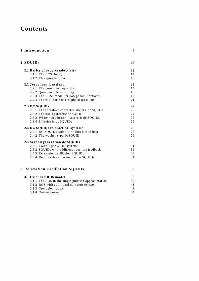
converted to a magnetic flux, for instance magnetic field, electric current ormechanical displacement, they have a wide field of applications. A well-knownexample is the detection of the very small magnetic signals that are producedby the human brain (magneto-encephalography) or heart (magneto-cardiography) [6]. An illustration of such a bio-magnetic measurement is shownin Fig. 1.1. Other applications are the readout of cryogenic particle detectorssuch as bolometers, superconducting tunnel junctions or gravitational waveantennae [7,8], non-destructive testing [6], susceptometers [9], picovoltmeters [10]
and magnetic microscopes [6,11].
Chapter 110
Essentially, a dc SQUID is a flux-to-voltage converter. Due to the limitedflux-to-voltage transfer of conventional dc SQUIDs, a sophisticated readoutconfiguration is required. This readout scheme, involving ac flux modulationtechniques and cooled step-up transformers between the dc SQUID and theroom temperature pre-amplifier, limits the versatility of standard dc SQUIDs.A major restriction caused by the readout scheme is for instance themeasurement bandwidth, which is typically below 100 kHz. Certainapplications, e.g. the readout of X-ray spectrometers based on superconductingtunnel junctions, require the outstanding sensitivity of a dc SQUID, but abandwidth considerably larger than that typical value.
Some imaging applications, such as bio-magnetism or non-destructivetesting, require many parallel channels for sufficient spatial resolution [6]. Insuch large systems, which can comprise as many as hundred or more SQUIDs,the standard flux modulated readout scheme can induce crosstalk betweenadjacent channels. Moreover, the cooled step-up transformers, which arelocated close to the SQUIDs, increase the complexity, and thus the productioncosts of the systems.
To avoid such complications, various “second generation” dc SQUIDs,enabling simpler readout schemes without degrading the sensitivity, have beendeveloped [12]. In the Low Temperature Division at the University of Twente,the development of second generation SQUIDs started in the early 1990’s withthe fabrication of relaxation oscillation SQUIDs (ROSs) and double relaxationoscillation SQUIDs (DROSs) [13], which are based on relaxation oscillations [14]
induced in hysteretic Josephson elements by an external L-R circuit. In thisthesis, the research concerning further improvement of (D)ROSs is described.
Figure 1.1 A magneto-cardiogram measured in the magnetically shieldedroom at the University of Twente. Details concerning the measurement systemwill be presented in section 4.3.

Introduction 11
In chapter 2, the basics of conventional dc SQUID systems are discussed,followed by a concise survey of various second generation dc SQUIDs, includingthe ROS and the DROS. The ROS, which is a flux-to-frequency converter, isdiscussed thoroughly in chapter 3. In that chapter, theoretical andexperimental ROS characteristics are presented.
The subject of chapter 4 is the DROS. Like conventional dc SQUIDs, aDROS is a flux-to-voltage transducer, but its flux-to-voltage transfer coefficientexceeds that of a standard dc SQUID by typically one order of magnitude. Thisallows a simple, reliable and fast readout scheme based on direct voltagedetection with a room temperature pre-amplifier. As the experimental resultspresented in chapter 4 indicate, the sensitivity of DROSs matches that ofstandard dc SQUIDs, notwithstanding the straightforward readout electronics.
As will be demonstrated in chapter 5, the output signal of a DROS isparticularly suited for digital readout, e.g. with integrated superconductingJosephson electronics. Potentially, such an integrated “smart DROS” sensorhas a very large measurement bandwidth. In addition, the number of wiresbetween the room temperature electronics and the SQUID sensors in a multi-channel system could be reduced substantially. Fully integrated smart DROSprototypes have been designed, fabricated and characterized. The experimentalcharacteristics showed that the devices operated according to the theoreticalexpectations. These results offer promising perspectives for futuredevelopments.
References1 R.C. Jaklevic, J.J. Lambe, A.H. Silver and J.E. Mercereau, “Quantum interference effects in
Josephson tunneling”, Phys. Rev. Lett. 12, 159-160 (1964).2 R.C. Jaklevic, J.J. Lambe, A.H. Silver and J.E. Mercereau, “Quantum interference from a
static vector potential in a field-free region”, Phys. Rev. Lett. 12, 274-275 (1964).3 R.C. Jaklevic, J.J. Lambe, J.E. Mercereau and A.H. Silver, “Macroscopic quantum
interference in superconductors”, Phys. Rev. 5A, 1628-1637 (1965).4 B.D. Josephson, “Possible new effects in superconductive tunneling”, Phys. Lett. 1, 251-253
(1962).5 J.G. Bednorz and K.A. Müller, “Possible high Tc superconductivity in the Ba-La-Cu-O
system”, Z. Phys. B 64, 189-193 (1986).6 J.P. Wikswo Jr., “SQUID magnetometers for biomagnetism and nondestructive testing:
Important questions and initial answers”, IEEE Trans. Appl. Supercond. 5, 74-120 (1995).7 N.E. Booth and D.J. Goldie, “Superconducting particle detectors”, Supercond. Sci. Technol.
9, 493-516 (1996).8 see, for instance, The detection of gravitational waves, ed. D.G. Blair, Cambridge University
Press, Cambridge (1993).9 M. Ketchen, D.J. Pearson, K. Stawiasz, C-K. Hu, A.W. Kleinsasser, T. Brunner, C. Cabral,
V. Chandrashekhar, M. Jaso, M. Manny, K. Stein, M. Bhushan, “Octagonal washerdc SQUIDs and integrated susceptometers fabricated in a planarized sub-µm Nb-AlOx-Nbtechnology”, IEEE Trans. Appl. Supercond. 3, 1795-1799 (1993).

Chapter 112
10 V. Polushkin, D. Drung and H. Koch, “A broadband picovoltmeter based on the directcurrent superconducting quantum interference device with additional positive feedback”,Rev. Sci. Instrum. 65, 3005-3011 (1994).
11 J.P. Wikswo Jr., “High-resolution magnetic imaging: cellular action currents and otherapplications”, in SQUID Sensors: Fundamentals, Fabrication and Applications, ed. H.Weinstock, NATO ASI Series 329, Kluwer Academic Publishers, Dordrecht / Boston /London (1996).
12 D. Drung, “Recent low temperature SQUID developments”, IEEE Trans. Appl. Supercond.4, 121-127 (1994).
13 D.J. Adelerhof, Second generation dc SQUID magnetometers: (Double) RelaxationOscillation SQUIDs, Ph.D. thesis University of Twente, Enschede (1993).
14 F.L. Vernon and R.J. Pedersen, “Relaxation oscillations in Josephson junctions”, J. Appl.Phys. 39, 2661-2664 (1968).

13
Chapter 2
SQUIDs
The operation principle of superconducting quantum interference devices(SQUIDs) is based on two phenomena inherent to superconductivity, namelythe macroscopic character of the superconducting wave function and theJosephson effects. These two keystones of superconducting electronics will bediscussed in sections 2.1 and 2.2, whereas the basic theory for the dc SQUIDwill be presented in section 2.3.
A dc SQUID is a non-linear flux-to-voltage converter and is generallyoperated as a null-detector in a feedback loop, the so-called flux locked loop. Insection 2.4, this flux locked loop and the conventional flux modulation schemewhich is used to match the low output impedance of the SQUID to the highinput impedance of the room temperature pre-amplifier are discussed. Forsome applications, for instance those requiring fast and simple electronics, thismodulated readout scheme is impractical or even unsuitable. To enableoperation without modulation schemes, various “second generation” dc SQUIDtypes, for example the relaxation oscillation SQUID and the double relaxationoscillation SQUID, have been developed. A short review of some commonsecond generation dc SQUIDs is given in section 2.5.
2.1 Basics of superconductivity
Before turning the attention to SQUIDs, some basic concepts ofsuperconductivity will be introduced in this section. When a superconductor iscooled below its critical temperature Tc, its electrical resistance vanishesabruptly. Another peculiar property of a superconductor is that it shows perfectdiamagnetism, a phenomenon known as the Meissner effect. In other words,both the electric field E and the magnetic field B are equal to zero in the bulk of

Chapter 214
the material. The expulsion of the magnetic field is caused by superconductingscreening currents in the surface layer. Within this layer, the magnetic fielddecreases exponentially over a characteristic length λL, the London penetrationdepth.
2.1.1 The BCS theory
The BCS theory [1], developed in 1957 by Bardeen, Cooper and Schrieffer, statesthat, due to the strong electron-phonon interaction in a superconductor, it isenergetically favourable for electrons to condense into pairs at the Fermienergy EF. As these Cooper pairs are bosons, they all occupy the same quantumstate, described by the macroscopic complex wave function Ψ. The squaredamplitude of this wave function, |Ψ|2, can be interpreted as the fraction of theconduction electrons which has condensed into Cooper pairs. Thus, in thenormal state, |Ψ| ≡ 0, and in the superconducting state it varies between0 and 1.
Figure 2.1 shows a semiconductor-like representation of the electronicdensity of states N(E) in a superconductor according to the BCS theory. As canbe seen, an energy gap ∆ is present at both sides of EF. For temperatures justbelow Tc, ∆ depends strongly on the temperature, whereas at lowertemperatures, i.e. below ∼Tc/2, the gap energy does not vary significantly withtemperature. At finite temperatures, some Cooper pairs are thermally excitedand form electron-like and hole-like charge carriers, the so-calledquasiparticles. In the semiconductor representation, the hole-like excitationsare modeled as missing electrons in the initially completely filled energy bandbelow EF.
Figure 2.1 Density of states in a superconductor at T > 0. The shaded regionsrepresent occupied electron-like states and the dots at E = EF symbolize Cooperpairs.

SQUIDs 15
2.1.2 Flux quantization
The phase difference ∆ϕ [2] of the superconducting wave function between twopoints P1 and P2 in a superconductor depends on the supercurrent density Js
and on the magnetic vector potential A, defined as B = rot A:
∆ϕ = +
⋅∫2 2
21
2πh
mn e
J eA dls
sP
P& & &
. (2.1a)
In Eq. (2.1a), h = 6.63⋅10-34 J⋅s is Planck’s constant, m = 9.11⋅10-31 kg representsthe mass of an electron, ns is the number of superconducting electrons per m3
and e = 1.60⋅10-19 C symbolizes the electric charge of an electron. Whencalculating the integral of Eq. (2.1a) along an arbitrary closed path within thesuperconductor, a phase difference of n⋅2π should result, otherwise Ψ would notbe single valued. Thus,
∆ϕ Φ
Φ Φ Φ
= ⋅ +
= ⋅
⇔
= ⋅ + = ⋅ = ⋅
∫
∫
22 2
2
22 0
π πm
hn eJ dl
eh
mn e
J dlhe
ss
ss
& &
& &
n
' n n .
(2.1b)
In this equation, n is an integer, Φ symbolizes the total magnetic flux enclosedby the path of integration, and the quantity Φ' represents the fluxoid.According to Eq. (2.1b), Φ' is quantized in units of Φ0 = h/2e = 2.07⋅10-15 Wb, theflux quantum.
Inside the bulk of a superconductor, Js = 0 and hence Eq. (2.1b) reduces inthis case to:
Φ Φ= ⋅n 0 . (2.1c)
As Eq. (2.1c) expresses, the magnetic flux in a superconducting loop isquantized in units of Φ0, a property known as flux quantization.
2.2 Josephson junctions
2.2.1 The Josephson equations
A Josephson tunnel junction consists of two superconducting electrodes whichare separated by a thin insulating barrier of thickness d. If d is sufficientlysmall, of the order of 1 nm, the superconducting wave functions in bothelectrodes are correlated. Because of this correlation, or weak link, Cooper pairscan tunnel between the two electrodes and a supercurrent can flow through the
Chapter 216
barrier without causing a voltage drop [3]. This Cooper pair tunnel current ICP
influences the phase difference φ between the wave functions in bothelectrodes, as is expressed by the dc Josephson equation:
I ICP = 0 sinφ . (2.2)
In Eq. (2.2), the critical current I0 represents the maximum value of ICP. If thecurrent through the junction is increased above I0, a voltage V will developacross the barrier. Because of this voltage, the phase difference φ changes intime. This phenomenon is described by the ac Josephson equation:
∂φ∂
πt
eV h= =
22
!!( ) . (2.3)
Equations (2.3) and (2.2) imply that a time-averaged voltage <V> across aJosephson junction causes an alternating Josephson current with a frequencyof fj = (2e/h)⋅<V> = (483.59767 MHz/µV)⋅<V>. This property can for instance beused for the construction of voltage standards.
2.2.2 Quasiparticle tunneling
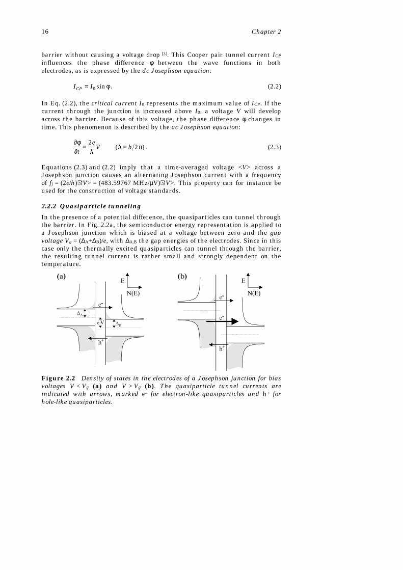
In the presence of a potential difference, the quasiparticles can tunnel throughthe barrier. In Fig. 2.2a, the semiconductor energy representation is applied toa Josephson junction which is biased at a voltage between zero and the gapvoltage Vg = (∆A+∆B)/e, with ∆A,B the gap energies of the electrodes. Since in thiscase only the thermally excited quasiparticles can tunnel through the barrier,the resulting tunnel current is rather small and strongly dependent on thetemperature.
Figure 2.2 Density of states in the electrodes of a Josephson junction for biasvoltages V < Vg (a) and V > Vg (b). The quasiparticle tunnel currents areindicated with arrows, marked e– for electron-like quasiparticles and h+ forhole-like quasiparticles.

SQUIDs 17
If the voltage is increased above Vg, this situation changes drastically. Then,electrons from the almost completely filled band below EF in one electrode cantunnel to the almost empty energy band above EF in the other electrode, asindicated by the large arrow in Fig. 2.2b. The result is a sharp increase of thequasiparticle tunnel current at V = Vg, as illustrated in Fig. 2.3, which showsthe experimental current vs. voltage (I-V) characteristic of a Nb/Al,AlOx/Al/NbJosephson junction.
For voltages much larger than Vg, the I-V characteristic of a Josephsontunnel junction has an Ohmic character with a normal resistance RN.
2.2.3 The RCSJ model for Josephson junctions
For quantitative analysis of circuitry containing Josephson junctions, the RCSJ(Resistively and Capacitively Shunted Junction) model, depicted schematicallyin Fig. 2.4, is widely used [4,5]. The cross symbolizes the Josephson element,which is described by Eqs. (2.2) and (2.3). The resistor Rj represents the non-linear resistance caused by tunneling of quasiparticles. Often, an additionalshunt resistor is connected across a Josephson junction to modify its properties.In this case, Rj represents the effective resistance of the shunt resistor and thequasiparticle resistance. The junction capacitance, Cj, depends on the thicknessand the dielectric constant of the barrier, and on the junction area.
The RCSJ model assumes that the phase difference φ between bothsuperconducting electrodes is constant over the whole junction area, or, in
Figure 2.3 Measured current vs. voltage characteristic of a 10 x 10 µm2
Nb/Al,AlOx/Al/Nb tunnel junction at T = 4.2 K. The inset gives an enlargementof the subgap region. The gap voltage of the junction is Vg = 2.8 mV. An externalmagnetic field was applied to suppress the critical current while recording thesubgap.
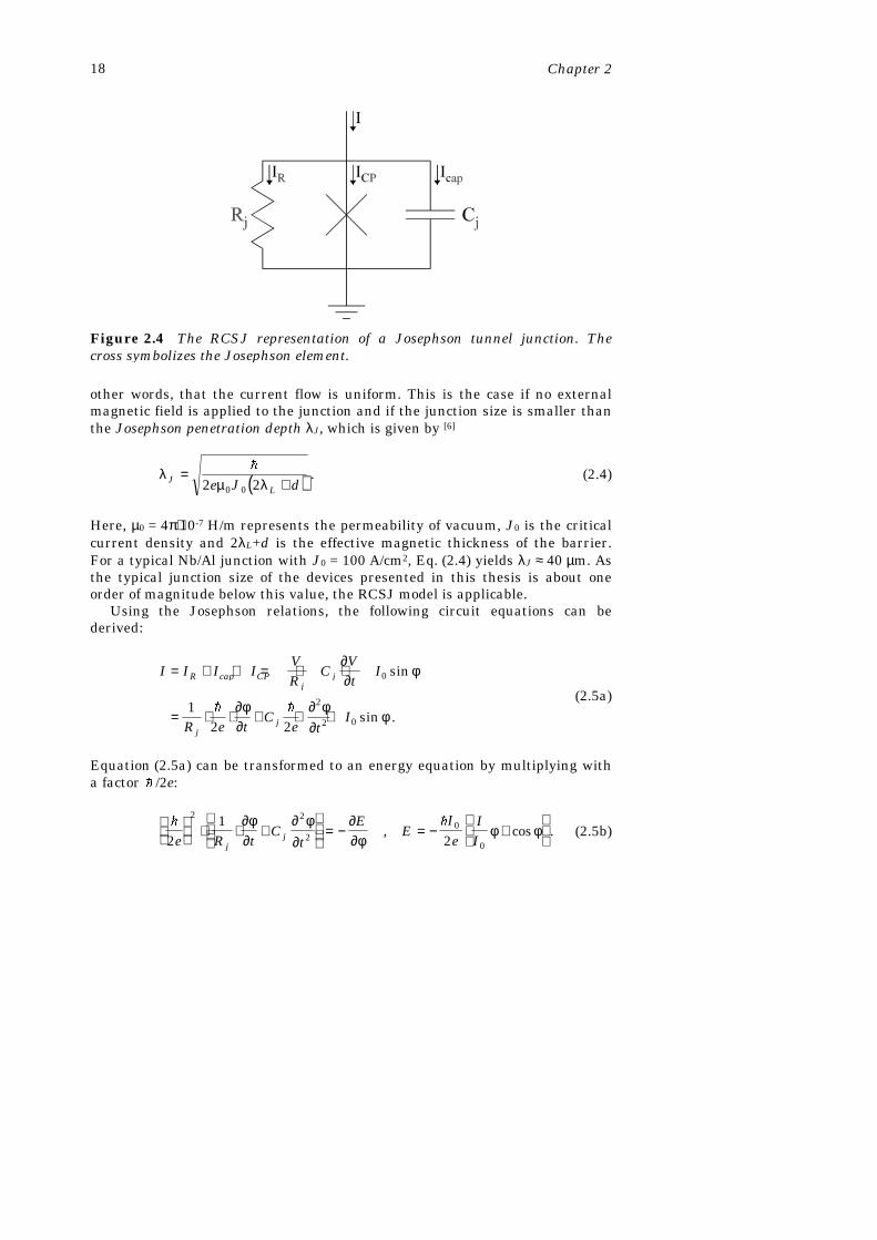
Chapter 218
other words, that the current flow is uniform. This is the case if no externalmagnetic field is applied to the junction and if the junction size is smaller thanthe Josephson penetration depth λJ, which is given by [6]
( )λµ λJ
Le J d=
+!
2 20 0. (2.4)
Here, µ0 = 4π⋅10-7 H/m represents the permeability of vacuum, J0 is the criticalcurrent density and 2λL+d is the effective magnetic thickness of the barrier.For a typical Nb/Al junction with J0 = 100 A/cm2, Eq. (2.4) yields λJ ≈ 40 µm. Asthe typical junction size of the devices presented in this thesis is about oneorder of magnitude below this value, the RCSJ model is applicable.
Using the Josephson relations, the following circuit equations can bederived:
I I I IVR
CVt
I
R e tC
e tI
R cap CPj
j
jj
= + + = + +
= ⋅ ⋅ + ⋅ +
∂∂
φ
∂φ∂
∂ φ∂
φ
0
2
2 01
2 2
sin
sin .! !
(2.5a)
Equation (2.5a) can be transformed to an energy equation by multiplying witha factor ! /2e:
! !
21
2
2 2
20
0e R tC
t
EE
Ie
IIj
j
⋅ ⋅ +
= − = − +
∂φ∂
∂ φ∂
∂∂φ
φ φ, cos . (2.5b)
Figure 2.4 The RCSJ representation of a Josephson tunnel junction. Thecross symbolizes the Josephson element.

SQUIDs 19
The factor ! I0/2e = I0Φ0/2π in Eq. (2.5b) represents the Josephson couplingenergy [3]. Equation (2.5b) can be interpreted with the mechanical analogue of aball moving in a “tilted washboard” potential [1] E, see Fig. 2.5. In this analogue,E represents the potential energy of the ball, the position of the ball is given byφ, the voltage across the junction is proportional to the velocity ∂φ/∂t, thecapacitance Cj corresponds to the mass of the ball, and the 1/Rj term representsthe viscous damping of the motion. The relative tilt of the washboard is givenby I/I0.
If |I| < I0, local potential wells exist in which the ball can be confined, asillustrated by trace (a) in Fig. 2.5. The trapped ball can oscillate back and fortharound its equilibrium position at the bottom of the well. The frequency ofthese plasma oscillations is given by the plasma frequency fp:
fI
CIIp
j= ⋅ −
0
0 0
2
42
1πΦ
, (2.6)
where the influence of Rj on fp has been neglected. During the plasmaoscillations, the average velocity of the ball (i.e. the voltage) is zero, implyingthat the junction is in the superconducting state. If the bias current exceeds thecritical current, the potential wells in the washboard vanish, as illustrated bytrace (b) in Fig. 2.5, and the ball starts to roll downhill. According to Eq. (2.3),the continuously increasing value of φ causes a voltage drop across the junction.If I » I0, the speed of the ball is only determined by the 1/Rj damping term andconsequently the junction is in the Ohmic regime.
When the junction is in the voltage state and the bias current is decreasedto a value below the critical current, the moving ball can be trapped again in
Figure 2.5 The tilted washboard model with I/I0 = 0.4 (a) and I/I0 = 1.3 (b).The ball moves through a viscous medium which causes damping of its motion.

Chapter 220
one of the potential wells, provided that the damping is large enough, i.e. thatRj is sufficiently small. The result is a non-hysteretic I-V characteristic, asshown in Fig. 2.6a. On the other hand, if the system is weakly damped (largeRj), the motion of the ball can persist at bias currents below the critical current.This causes a hysteretic I-V characteristic, like the one already shown inFig. 2.3.
The value of the McCumber parameter, defined as
βπ
Cj jI R C
=2 0
2
0Φ, (2.7)
determines to which degree a junction shows hysteresis. If βC « 1, the junctionis non-hysteretic, and if βC » 1, the junction has a hysteretic I-V characteristic.Between the two extreme situations of Fig. 2.3 and Fig. 2.6a, junctions withmoderate hysteresis exist, see e.g. Fig. 2.6b.
In hysteretic Josephson junctions, the voltage state can only persist for biascurrents larger than the minimum return current, Imin, indicated in Fig. 2.6b.Several expressions relating the minimum return current to the value of βC canbe found in the literature [7,8]. For βC » 1,
I IminC
≈4
0π β. (2.8a)
Figure 2.6 Measured current vs. voltage characteristics of resistively shuntedNb/Al,AlOx/Al/Nb tunnel junctions at T = 4.2 K. (a) Non-hysteretic junctionwith I0 = 4 µA, Rshunt = 6.8 Ω and βC ≈ 0.3. (b) Hysteretic junction withI0 = 60 µA, Rshunt = 28 Ω and βC ≈ 50.

SQUIDs 21
When highly hysteretic junctions are considered, the concept of minimumreturn voltage, Vmin, is more appropriate than the minimum return current.Using Vmin = Imin⋅Rj, the following expression can be derived from Eq. (2.8a):
V I RI
Cmin min jj
= ⋅ =4
20 0
π πΦ
. (2.8b)
Note that Rj does not appear explicitly in the expression for Vmin.An alternative approach to derive an expression for Vmin is the following. If a
junction is biased at an average voltage Vdc, the ac Josephson current has anamplitude of I0 and a frequency of fj = (2e/h)⋅Vdc. Neglecting the current throughRj and the non-harmonic character of the Josephson oscillations, the oscillatingJosephson current causes an ac voltage across the capacitance Cj with anamplitude of Vac = I0/(2πfjCj) = I0Φ0/(2πCjVdc). If Vac ≈ Vdc, the junction voltageapproaches zero each oscillation period. Obviously, the junction can easily betrapped in the V = 0 state in this situation. Taking Vmin to be that value of Vdc
where Vdc = Vac, one obtains Vmin = √(I0Φ0/2πCj), which is equal to Eq. (2.8b),apart from the factor 4/π (≈ 1.3).
2.2.4 Thermal noise in Josephson junctions
The discussion of the RCSJ model in the previous section did not include theeffect of thermal noise. Like in any system, also the total energy of a Josephsonjunction, expressed by Eq. (2.5b), is subject to thermal fluctuations of the orderkBT, where kB = 1.38⋅10-23 J/K is the Boltzmann constant. To prevent thejunction dynamics from being wiped out by the thermal fluctuations, thesefluctuations should be small compared to the Josephson coupling energy ofI0Φ0/2π. The ratio between the thermal energy and the Josephson couplingenergy is expressed by the noise rounding parameter Γ:
ΓΦ Φ
= =k T
Ik T
IB B
0 0 0 022
ππ
. (2.9)
Computer simulations indicate that for Γ < 0.2, the effect of thermalfluctuations is negligibly small [9]. In practice, often a “safer” criterion, namelyΓ < 0.05, is used. At 4.2 K, the latter value of Γ implies a minimum criticalcurrent of 3.5 µA.
In hysteretic junctions, thermal fluctuations can cause a premature (i.e. atI < I0) transition from the superconducting state to the voltage state, as will bediscussed in detail in section 3.2. In non-hysteretic junctions, the thermalfluctuations can cause the ball to roll out of a potential minimum into the nextone from time to time. If this happens, small voltage pulses, randomly spacedin time, are produced, which causes noise rounding of the I-V characteristic atI ≈ I0, like indicated in Fig. 2.6a.

Chapter 222
In resistively shunted junctions, the Johnson noise generated by the shuntresistor R, having a spectral density SI of
S k T RI B= 4 / , (2.10)
also contributes to the noise. This noise source can be modeled by adding anoise term to the bias current. In the mechanical analogue, the Johnson noisecauses fluctuations in the tilt of the washboard. Hence, also the Johnson noisegenerated by the junction shunt resistor can cause the ball to escape from apotential well in the washboard at bias currents below I0.
Equation (2.10) only holds in the classical limit f < kBT/h, with f thefrequency. All devices presented in this thesis operate within this limit. Fordevices operating at a very high frequency or at extremely low temperatures,Eq. (2.10) is no longer valid and zero point fluctuations, the quantummechanical counterpart of Johnson noise, become important [10,11].
2.3 DC SQUIDs
Roughly speaking, SQUIDs can be divided into two families: rf SQUIDs anddc SQUIDs. An rf SQUID is based on only one Josephson junction whereasdc SQUIDs have two identical junctions. Until the early 1980’s, the rf SQUIDwas widely used because the reproducible fabrication of two identicalJosephson junctions was problematic. When production techniques becamemature, the dc SQUID took the leading role because of its better sensitivity,although the discovery of the ceramic high Tc superconductors in 1986 renewedthe interest for rf SQUIDs [12]. Since all devices in this thesis are based onlow Tc dc SQUIDs, the discussion in this section will be restricted to thesedevices.
2.3.1 The threshold characteristic of a dc SQUID
Figure 2.7 shows a schematic picture of a dc SQUID, consisting of two identicalJosephson junctions with a critical current I0, connected in parallel by asuperconducting loop with inductance Lsq. The junctions can be shunted withan external resistor R to remove the junction hysteresis. A dc bias current Ib
- hence the name dc SQUID - is injected symmetrically into the SQUID loop.This bias current distributes over the two junctions:
( )I I I Ib = + = +1 2 0 1 2sin sinφ φ , (2.11)
where φ1 and φ2 represent the phases of both junctions.

SQUIDs 23
The superconducting SQUID ring has to comply with the flux quantizationcondition (section 2.1.2), taking into account the phases φ1 and φ2:
2 20
1 2π φ φ πΦΦ
tot + − = ⋅n . (2.12)
In this equation, Φtot represents the total magnetic flux comprised by theSQUID loop, i.e. the sum of the applied signal flux Φsig and the flux caused bythe circulating screening current Iscr:
Φ Φtot sig sq scr scrL I II I
= − ⋅ =−
, 2 1
2. (2.13)
If the signal flux Φsig equals n⋅Φ0, no screening current flows in the SQUIDloop and the bias current is divided symmetrically over the two junctions:I1 = I2 = Ib/2. In this case, the critical current Ic of the SQUID is just the sum ofthe critical currents of the junctions: Ic(Φsig = n⋅Φ0) = 2I0. For other values ofthe flux, the screening current is non-zero, which causes an imbalance betweenI1 and I2. Therefore, the current through one of the junctions reaches its criticalvalue already for Ib < 2I0 and, consequently, the critical current of the SQUID issuppressed if Φsig ≠ n⋅Φ0.
Qualitatively, the I-V characteristic of a hysteretic dc SQUID (havingjunctions with βC » 1) looks like that of a single hysteretic Josephson junction,see e.g. Fig. 2.3. The large difference is that the critical current of thedc SQUID can be modulated with the signal flux Φsig which is applied to theSQUID loop. Figure 2.8 shows an experimental Ic-Φsig characteristic (threshold
Figure 2.7 Scheme of a dc SQUID. The Josephson junctions are representedby crosses, the shunt resistors are optional. The signal flux Φsig is applied to thesuperconducting SQUID loop.

Chapter 224
curve) of a hysteretic dc SQUID. The characteristic was recorded by sweepingthe signal flux at a slow rate (∼0.1 Hz) while the bias current was swept fromzero to ∼100 µA at a considerably larger frequency (∼100 Hz). The transitionfrom V = 0 to V = Vg was used to trigger an analogue-to-digital converter whichmeasured both the bias current and the signal flux at the transition point. Thesolid line in Fig. 2.8 represents a theoretical fit to the measured data. Theunderlying model is based on Eqs. (2.11) to (2.13) [13].
The measurements in Fig. 2.8 show that Ic(Φ) is not single-valued ifΦsig ≈ (m+½)⋅Φ0. The reason is that for Φsig ≈ (m+½+δ)⋅Φ0, with |δ| « 1, thevalue of the integer n in Eq. (2.12) can be either n = m or n = (m+1). If δ > 0, then = (m+1) state is energetically preferred since it corresponds to the smallestscreening current, and, on the other hand, if δ < 0, the n = m state is morelikely to occur.
2.3.2 The non-hysteretic dc SQUID
Most low Tc dc SQUIDs are based on resistively shunted, non-hystereticJosephson tunnel junctions. Figure 2.9a shows the schematic I-V characteristicof a non-hysteretic dc SQUID for two different values of the signal flux. IfΦsig = n⋅Φ0, the critical current of the dc SQUID has its maximum value ofIc = Ic,max = 2I0 and, on the other hand, if Φsig = (n+½)⋅Φ0, the critical current isminimum, viz. Ic = Ic,min.
Figure 2.8 Markers: experimental threshold characteristic of a hystereticdc SQUID. The solid line gives a theoretical fit to the experimental data. Fromthis fit, a SQUID inductance of Lsq = 32 pH (±10%) was deduced.

SQUIDs 25
The modulation depth ∆Ic of the critical current can be calculated as [13]
∆I I I Ic c,max c,minL
= − ≈+
⋅1
12 0β
(2.14)
if the screening parameter βL, defined as
βLsqI L
=2 0
0Φ, (2.15)
is of the order of 100. The horizontal dotted line in Fig. 2.9a corresponds to afixed bias current, slightly larger than the maximum critical current of theSQUID. If Φsig is varied, the voltage across the SQUID swings between V1 andV2. Thus, a current biased non-hysteretic dc SQUID is a flux-to-voltageconverter. The corresponding voltage vs. flux characteristic is shown inFig. 2.9b. From computer simulations, the maximum slope of the V-Φsig
characteristic, generally referred to as the flux-to-voltage transfer, was derivedto be [9]
∂∂Φ
ββ
V RLsig
L
L sq≈
+⋅
21
. (2.16)
For optimized dc SQUIDs, βL should be close to unity [9], in which caseEq. (2.16) reduces to ∂V/∂Φsig ≈ R/Lsq.
Figure 2.9 (a) Schematic Ib-V and (b) V-Φsig characteristics of a non-hysteretic dc SQUID.

Chapter 226
2.3.3 White noise in non-hysteretic dc SQUIDs
The main noise source in resistively shunted dc SQUIDs - at least attemperatures around 4.2 K - is the Johnson noise generated in the shuntresistors R, causing a voltage noise of
S SVI
k TRV Ib
B= ⋅ ⋅
≈ ⋅γ
∂∂
γ2 22
(2.17a)
at the output of the SQUID. In Eq. (2.17a), the dynamic resistance ∂V/∂Ib of theSQUID was approximated with R/2 and the noise of both shunt resistors wasconsidered to be uncorrelated. The factor γ arises from the fact that Johnsonnoise, generated at frequencies around the Josephson frequency, is mixed downto lower frequencies by the Josephson oscillations and the inherent non-linearity of the junctions. Computer simulations showed that γ ≈ 8 [9]. DividingSV by (∂V/∂Φsig)2, the flux noise spectral density, SΦ, can be derived:
( )S
S
V
k TL
RV
sig
B sqΦ = ≈ ⋅
∂ ∂Φγ2
22, (2.17b)
where βL was set to unity. A typical low Tc dc SQUID, operating at 4.2 K, has aflux noise of the order of √SΦ ≈ 1 µΦ0/√Hz.
To compare the sensitivity of SQUIDs with different inductances, the energyresolution ε is commonly used :
ε γ= ≈ ⋅SL
k TL
RsqB
sqΦ
2. (2.17c)
When deriving Eq. (2.17a), only the in-phase components of the Johnsonnoise currents generated by both shunt resistors were taken into account. Theout-of-phase components induce a noise current IN in the SQUID loop whichgenerates a flux noise ΦN = IN⋅Lsq [14]. For most applications, this effect is notimportant, and only in a few particular cases, e.g. when using a SQUID as atuned radio frequency amplifier, it is significant. In this case, ΦN induces anoise current in the tuned input circuit (back action), which current on its turngenerates additional flux noise in the SQUID loop.
2.3.4 1/f noise in dc SQUIDs
At low frequencies, the flux noise spectral density of practical dc SQUIDsincreases with a 1/f character. Two mechanisms for this 1/f noise have beenidentified, namely fluctuations of the critical current and motion of flux lineswithin the SQUID body [15].

SQUIDs 27
The critical current fluctuations are caused by the presence of energy trapsin the tunnel barriers of the junctions. When a tunneling electron is capturedin one of these local energy wells, the critical current density changes. After arandom time, the trapped electron is released, and the local critical currentdensity is restored. The telegraph noise generated by the random trapping ofelectrons in several independent localized states in the barrier causes a 1/f-likenoise spectrum. With high quality Josephson junctions, having low excesscurrents in the subgap region, this 1/f noise source can be reduced significantly.Moreover, specific modulation techniques, in which the SQUID is biased withan ac instead of a dc bias current, can be advantageous in reducing the 1/f noisedue to critical current fluctuations [16,17].
The second origin of 1/f noise, the motion of trapped magnetic flux lines, isassociated with the quality and microstructure of the material of the SQUIDbody. If a SQUID is placed in an ambient field, e.g. the earth’s magnetic field(∼ 50 µT), magnetic flux lines can penetrate the SQUID body, for instance atmaterial defects. These flux lines cause a magnetic flux in the SQUID whichchanges when the flux lines move randomly from one pinning center toanother. Since this noise manifests itself as “real” flux noise, it can not bereduced with modulation schemes. The motion of flux lines can be restricted byintroducing strong pinning centers (“moats”) in the SQUID body to trap themoving flux lines [18]. Another approach is to decrease the size of thesuperconducting structures in the SQUID body, so that the flux penetration inthe superconducting material is strongly reduced [19].
2.4 DC SQUIDs in practical systems
2.4.1 DC SQUID readout: the flux locked loop
For many applications, the non-linear V-Φsig characteristic of a dc SQUID is notsuitable. By using the SQUID as null detector in a feedback loop, its responsecan be linearized. Figure 2.10 shows a schematic diagram of such a flux lockedloop (FLL) configuration.
Figure 2.10 Basic flux locked loop configuration without flux modulation.

Chapter 228
When a SQUID is operated in a FLL, in addition to the signal flux, afeedback flux (Φfb) is applied by means of a coil in the vicinity of the SQUID.The feedback loop keeps the output voltage of the SQUID, and hence the totalflux Φsig + Φfb, constant. Thus, if the signal flux changes by an amount ∆Φsig,the feedback flux changes by an amount ∆Φfb = -∆Φsig:
∆Φ ∆ ∆Φ ∆ ∆Φfbfb
fbFLL sig FLL
fb
fbsig
M
RV V
R
M= ⋅ = − → = − ⋅ . (2.18)
As Eq. (2.18) shows, the dependence between the output voltage of the fluxlocked loop (VFLL) and the input flux (Φsig) is linear and only dependent on thefeedback parameters Rfb and Mfb.
The output voltage noise √SV of a dc SQUID at the flux locking point is givenby √SV = √SΦ⋅(∂V/∂Φ). With √SΦ = 1 µΦ0/√Hz and ∂V/∂Φ = 100 µV/Φ0, which aretypical values for a dc SQUID operating at 4.2 K, this yields an output voltagenoise of √SV = 0.1 nV/√Hz. This is about one order of magnitude below the inputvoltage noise of a room temperature dc amplifier. Therefore, the FLL scheme ofFig. 2.10 leads to amplifier limitation of the system sensitivity. To overcomethis situation, the FLL configuration of Fig. 2.11 is commonly used. In thisscheme, a modulating flux with a peak-to-peak amplitude of ½Φ0 is applied tothe SQUID, usually via the same coil which is used for the feedback flux. Thisenables the use of ac impedance matching circuitry, e.g. a cooled resonant L-Ccircuit or a resonant step-up transformer, between the SQUID and the pre-amplifier [15]. An additional benefit of this flux modulated readout scheme isthat the signal spectrum is shifted towards the sidebands of the modulationfrequency, which eliminates the 1/f noise contribution of the pre-amplifier.
Various sophisticated modulation schemes, in which not only the flux, butalso the bias current is modulated, have been developed [16,17]. With such biasreversal schemes, the 1/f noise generated by critical current fluctuations can besuppressed considerably, although the white noise level might increase slightly.
Figure 2.11 Flux locked loop configuration with flux modulation and resonantstep-up transformer.

SQUIDs 29
2.4.2 The washer-type dc SQUID
At present, most high performance dc SQUIDs are made in thin filmtechnology. A commonly used thin film configuration, the washer-typedc SQUID with tightly coupled input coil, is shown in Fig. 2.12. In thisconfiguration, the SQUID inductance is composed of a square washer, whichhas an inductance of [20]
L dw = ⋅ ⋅125 0. µ , (2.19)
provided that the outer size of the washer is much larger than the hole width d,and that the thickness of the washer is at least 2λL to ensure a completeMeissner effect. The inductance of the slit in the washer, which also contributesto the total SQUID inductance, is not taken into account in Eq. (2.19).Typically, this slit inductance amounts to 0.3 .. 0.4 pH per µm length [21].Generally, for low Tc materials like niobium, the kinetic inductance gives nomajor contribution to the total SQUID inductance [22].
The superconducting multi-turn input coil on top of the washer enablesefficient coupling to the outside world. The inductance of the input coil, Lin, isgiven by [20]
L n Lin w≈ 2 , (2.20a)
with n the number of turns of the input coil.
Figure 2.12 Washer-type dc SQUID with integrated multi-turn input coil. Theshunt resistors of the Josephson junctions are not indicated.
Chapter 230
The mutual inductance between the input coil and the SQUID inductanceamounts to
M k L L k n Lin in sq w= ≈ ⋅ ⋅ . (2.20b)
In practice, the coupling coefficient k can be close to unity, with typical valuesabove 0.8.
To compare the sensitivity of dc SQUIDs with integrated input coils, thecoupled energy resolution εcoupl should be used instead of the intrinsic energyresolution ε [cf. Eq. (2.17c) ] to account for different coupling efficiencies [23]:
εε
couplin I in
in
L S L SM k
= = =2 2 2 2
Φ . (2.21)
In this equation, SI = SΦ/Min2 represents the equivalent current noise spectraldensity referred to the input coil.
The parasitic capacitance between the SQUID washer and the input coil hasa negative influence on the SQUID dynamics [24]. Moreover, standing waves canoccur in the input coil due to its transmission line geometry. These resonancephenomena cause irregularities in the V-Φsig and I-V characteristics at voltageswhere the Josephson frequency is equal to one of the resonance frequencies. Atthese resonant points, the SQUID performance is degraded considerably.Therefore, proper damping of these resonances is essential. This can beachieved by adding an extra shunt resistor across the SQUID inductance todamp L-C oscillations in the SQUID loop [25], and by connecting an R-C shuntacross the input coil to attenuate the microwave resonances in the inputcoil [26]. Recently, a novel solution, in which each turn of the input coil isshunted by a separate resistor (intra coil damping) was presented [27]. Anotherrecent development is the use of distributed eddy current damping filters ontop of the input coil [28]. Also, intermediate flux transformers can be used inorder to decrease the size of the input coil, thus reducing the parasiticcapacitance [24].
2.5 Second generation dc SQUIDs
Unfortunately, the flux modulated readout mode discussed in section 2.4.1 hassome drawbacks. Usually, the matching circuitry is located near the SQUID,i.e. in the cryogenic environment. Especially in large multi-channel systems, asfor instance used for bio-magnetism, careful screening is required to minimizethe crosstalk between the matching transformers and the SQUIDs. Thisincreases the complexity of the system, and thus the production costs,considerably. Furthermore, the bandwidth of a flux modulated FLL is limitedby the modulation frequency, which is in the range 100 .. 500 kHz for most

SQUIDs 31
systems, although a system operating at a modulation frequency of 16 MHz hasbeen reported [29,30]. For some applications, such as the readout of X-raydetectors based on superconducting tunnel junctions [31], this restrictedbandwidth is a serious disadvantage.
To allow flux locked loop operation with the simple direct voltage readoutscheme of Fig. 2.10, several SQUID types with a larger flux-to-voltage transferhave been developed, and a few of them will be discussed below.
2.5.1 Two-stage SQUID systems
The transfer coefficient of a dc SQUID can be increased by using a secondSQUID as a pre-amplifier. In such a configuration, the sensor SQUID can beoptimized with respect to noise, whereas the readout SQUID can be designed toyield maximum output. Two-stage systems with a readout stage consisting of aseries array of 100 to 200 dc SQUIDs [32] have been commercialized byHYPRES [33]. A schematic diagram of such a device is shown in Fig. 2.13.
A small resistor Rx (∼50 mΩ) is used to bias the sensor SQUID at a constantvoltage. The flux dependent current Isens(Φsig) generated by the sensor SQUIDflows through the input coils of the SQUID array. If all SQUIDs in the arraymodulate coherently, their individual V-Φ characteristics add constructively,which results in a large voltage swing at the output.
Figure 2.13 Two-stage dc SQUID with a SQUID array as the second stage.The shunt resistors across the junctions are not shown.
Chapter 232
For devices like this, an output voltage swing of about 8 mV [34], a flux-to-voltage transfer of ∂Vout/∂Φsig > 20 mV/Φ0 and a white energy resolution ofε ≈ 30 h (εcoupl ≈ 310 h) have been reported [32]. A disadvantage of the device isits susceptibility to flux trapping. If flux is trapped in the SQUIDs of the array,their V-Φ characteristics are shifted with respect to one another. As a result,the V-Φ curves no longer add constructively and the voltage modulation depthis decreased drastically.
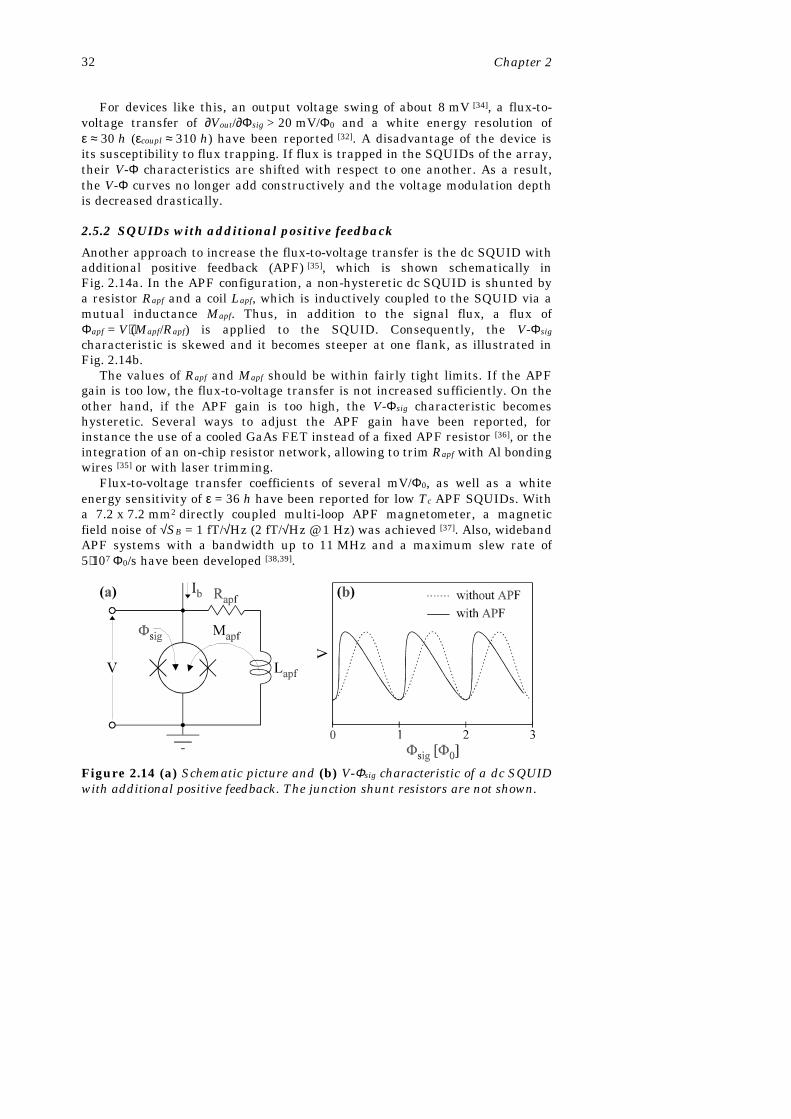
2.5.2 SQUIDs with additional positive feedback
Another approach to increase the flux-to-voltage transfer is the dc SQUID withadditional positive feedback (APF) [35], which is shown schematically inFig. 2.14a. In the APF configuration, a non-hysteretic dc SQUID is shunted bya resistor Rapf and a coil Lapf, which is inductively coupled to the SQUID via amutual inductance Mapf. Thus, in addition to the signal flux, a flux ofΦapf = V⋅(Mapf/Rapf) is applied to the SQUID. Consequently, the V-Φsig
characteristic is skewed and it becomes steeper at one flank, as illustrated inFig. 2.14b.
The values of Rapf and Mapf should be within fairly tight limits. If the APFgain is too low, the flux-to-voltage transfer is not increased sufficiently. On theother hand, if the APF gain is too high, the V-Φsig characteristic becomeshysteretic. Several ways to adjust the APF gain have been reported, forinstance the use of a cooled GaAs FET instead of a fixed APF resistor [36], or theintegration of an on-chip resistor network, allowing to trim Rapf with Al bondingwires [35] or with laser trimming.
Flux-to-voltage transfer coefficients of several mV/Φ0, as well as a whiteenergy sensitivity of ε = 36 h have been reported for low Tc APF SQUIDs. Witha 7.2 x 7.2 mm2 directly coupled multi-loop APF magnetometer, a magneticfield noise of √SB = 1 fT/√Hz (2 fT/√Hz @ 1 Hz) was achieved [37]. Also, widebandAPF systems with a bandwidth up to 11 MHz and a maximum slew rate of5⋅107 Φ0/s have been developed [38,39].
Figure 2.14 (a) Schematic picture and (b) V-Φsig characteristic of a dc SQUIDwith additional positive feedback. The junction shunt resistors are not shown.

SQUIDs 33
2.5.3 Relaxation oscillation SQUIDs
As Fig. 2.15a shows, a relaxation oscillation SQUID (ROS) consists of ahysteretic dc SQUID, shunted by a resistor Rsh and an inductor Lsh, which isnot magnetically coupled to the SQUID. If a ROS is biased with an appropriatedc bias current Ib > Ic(Φsig), relaxation oscillations are generated [40,41]. Athorough discussion of the dynamics of the ROS will be given in chapter 3, thediscussion in this section is restricted to a simple model to clarify its principleof operation.
Let us assume that at a time t = 0 the current I1 through the SQUID branchis zero, so that the SQUID is in the superconducting state. Since I1 + I2 = Ib andI1 = 0, it follows that I2 = Ib. Because V = 0, the current I2 decays exponentiallywith a time constant Lsh/Rsh. Consequently, I1 increases, as is indicated inFig. 2.15b. After a time T0, given by [41]
( )TLR
I
I Ish
sh
b
b c sig0 =
−
ln
Φ, (2.22a)
the current through the hysteretic dc SQUID reaches its critical value Ic(Φsig),and the SQUID switches to the gap voltage Vg.
In the presence of the voltage V = Vg, the current I2 through the Lsh-Rsh
shunt increases again, and consequently the current through the SQUID, I1,decreases. After having spent a time TV, given by [41]
( )T
LR
R I
V R IVsh
sh
sh c sig
g sh b= +
−
ln 1
Φ, (2.22b)
Figure 2.15 (a) Scheme of a relaxation oscillation SQUID (ROS). (b) I1-t andV-t traces of a current biased ROS.

Chapter 234
in the voltage state, the current through the SQUID has decayed to zero, theSQUID switches back to the superconducting state, and the whole cycle startsagain, as shown in Fig. 2.15b.
As a result of the relaxation oscillation process, voltage pulses with anamplitude Vg and a frequency fRO of
fT T TRO
V=
+≈
1 1
0 0(2.23)
are generated at the ROS output. The right-hand approximate expression inEq. (2.23) is justified by the fact that, generally, T0 » TV.
Since both T0 and TV depend on the critical current of the dc SQUID, fRO is afunction of the applied flux, which makes a ROS a flux-to-frequency converter.Because T0 and TV have a different dependence on Ic(Φsig), the time-averagedvoltage <V> across the ROS, calculated as
< > =+
VT
T TVV
Vg
0, (2.24)
is also modulated by the signal flux. Consequently, a ROS can be used either infrequency or in voltage readout mode. However, as will be shown in chapter 3,the flux-to-voltage transfer of a ROS with voltage readout is comparable to thatof a standard non-hysteretic dc SQUID, which implies that a ROS with voltagereadout does not have significant advantages compared to standarddc SQUIDs. Therefore, frequency readout is the appropriate readout scheme fora ROS.
The sensitivity of a ROS depends on the relaxation frequency. Typically,optimum noise performance is achieved at a relaxation frequency around1 GHz.
Various uncoupled ROSs have been presented in literature, with relaxationfrequencies ranging from a few MHz [42,43] to 7 GHz [40,44]. The best reportedenergy sensitivity, measured in a FLL with frequency readout at roomtemperature, is ε ≈ 600 h [40].
2.5.4 Double relaxation oscillation SQUIDs
Figure 2.16a shows a schematic diagram of a double relaxation oscillationSQUID (DROS). Contrary to the ROS, which is operated with frequencyreadout, the DROS is designed for direct voltage readout. In a DROS, theexternal Lsh-Rsh circuit shunts two hysteretic dc SQUIDs, the signal SQUIDand the reference SQUID. The signal flux Φsig is applied to the signal SQUID,whereas a constant reference flux Φref is applied to the reference SQUID. In apredecessor of the DROS, the signal flux was applied to both SQUIDs.However, this device, the balanced ROS [45], will not be discussed here. Bytuning Φref, the critical current of the reference SQUID can be adjusted to a

SQUIDs 35
value in the middle of the critical current modulation range of the signalSQUID, as indicated in the schematic Ic-Φsig graph in Fig. 2.16b.
If a DROS is biased with a dc bias current, relaxation oscillations aregenerated under the same conditions as for a ROS. The main difference with aROS is that a DROS acts as a critical current comparator. Only the SQUIDwith the smallest critical current participates in the relaxation oscillations,while the other SQUID remains superconducting. As a consequence, the outputvoltage, which is measured across the reference SQUID, equals zero whenIc,sig(Φsig) < Ic,ref. On the other hand, when the signal flux is changed in such away that Ic,sig(Φsig) > Ic,ref, voltage pulses with a frequency fRO arise at the DROSoutput. If an amplifier with a bandwidth considerably smaller than fRO is usedfor readout, only the time-averaged dc component <V> = Vc of these pulses ismeasured. The resulting <V>-Φsig characteristic has a modulation depth Vc anda large flux-to-voltage transfer at the points where Ic,ref = Ic,sig(Φsig), as sketchedin the lower trace of Fig. 2.16b.
As for a ROS, the optimum relaxation frequency for a DROS is typically1 GHz [41]. Typical values for the flux-to-voltage transfer are in the order of∂V/∂Φsig ≈ 1 mV/Φ0 and the best intrinsic energy resolution reported for anuncoupled DROS is ε = 13 h (34 h in FLL) [46]. The best reported energysensitivity of a DROS with an integrated input coil is ε ≈ 150 h in FLL(εcoupl ≈ 300 h) [47]. In chapter 4, the DROS will be discussed in more detail.
Figure 2.16 (a) Scheme of a double relaxation oscillation SQUID (DROS).(b) Ic-Φsig and <V>-Φsig graphs for a DROS.

Chapter 236
References1 M. Tinkham, Introduction to superconductivity, McGraw-Hill International Editions, New
York etc., 2nd edition (1996).2 B.W. Petley, An Introduction to the Josephson Effects, Mills & Boon Ltd., London (1971).3 B.D. Josephson, “Possible new effects in superconductive tunneling”, Phys. Lett. 1, 251-253
(1962).4 W.C. Stewart, ”Current-voltage characteristics of Josephson junctions”, Appl. Phys. Lett. 12,
277-280 (1968).5 D.E. McCumber, “Effect of ac impedance on dc voltage-current characteristics of
superconductor weak-link junctions”, J. Appl. Phys. 39, 3113-3118 (1968).6 J.R. Waldram, A.B. Pippard and J. Clarke, “Theory of the current-voltage characteristics of
SNS junctions and other superconducting weak links”, Phil. Trans. Roy. Soc. Lond. A 268,265-287 (1970).
7 H.H. Zappe, “Minimum current and related topics in Josephson tunnel junction devices”, J.Appl. Phys. 44, 1371-1377 (1972).
8 A.T. Johnson, C.J. Lobb and M. Tinkham, “Effect of leads and energy gap upon theretrapping current of Josephson junctions”, Phys. Rev. Lett. 65, 1263-1266 (1990).
9 C.D. Tesche and J. Clarke, “DC SQUID: noise and optimization”, J. Low Temp. Phys. 29,301-331 (1977); J.J.P. Bruines, V.J. de Waal and J.E. Mooij, “Comment on: ‘DC SQUID:noise and optimization’ by Tesche and Clarke”, J. Low Temp. Phys. 46, 383-386 (1982).
10 R.H. Koch, D.J. van Harlingen, J. Clarke, “Quantum-noise theory for the resistivelyshunted Josephson junction”, Phys. Rev. Lett. 45, 2132-2135 (1980).
11 C.W. Gardner, Quantum Noise, Springer-Verlag, Berlin / Heidelberg (1991).12 Y. Zhang, N. Wolters, X.H. Zeng, J. Schubert, W. Zander, H. Soltner, M. Banzet, F. Rüders
and A.I. Braginski, “Washer rf SQUID magnetometers with coplanar resonators at 77 K”, inextended abstracts ISEC’97 conference, ed. H. Koch and S. Knappe, P.T.B. Braunschweig,51-53 (1997).
13 R.L. Peterson and C.A. Hamilton, “Analysis of threshold curves for superconductinginterferometers”, J. Appl. Phys. 50, 8135-8142 (1979).
14 C.D. Tesche and J. Clarke, “DC SQUID: current noise”, J. Low Temp. Phys. 37, 397-403(1979).
15 J. Clarke, “SQUID fundamentals”, in SQUID Sensors: Fundamentals, Fabrication andApplications, ed. H. Weinstock, NATO ASI Series 329, Kluwer Academic Publishers,Dordrecht / Boston / London (1996).
16 R.H. Koch, J. Clarke, J.M. Martinis, W.M. Goubau, C.M. Pegrum and D.J. van Harlingen,“Investigation of 1/f noise in tunnel junction dc SQUIDs”, IEEE Trans. Magn. 19, 449-452(1983).
17 V. Foglietti, W.J. Gallagher, M.B. Ketchen, A.W. Kleinsasser, R.H. Koch, S.I. Raider andR.L. Sandstrom, “Low-frequency noise in low 1/f noise dc SQUID’s”, Appl. Phys. Lett. 49,1393-1395 (1986).
18 M. Jeffery, T. Van Duzer, J.R. Kirtley and M.B. Ketchen, “Magnetic imaging of moat-guarded superconducting electronic circuits”, Appl. Phys. Lett. 67, 1769-1771 (1995).
19 E. Dantsker, S. Tanaka and J. Clarke, “High-Tc superconducting quantum interferencedevices with slots or holes: Low 1/f noise in ambient magnetic fields”, Appl. Phys. Lett. 70,2037-2039 (1997).
20 J.M. Jaycox and M.B. Ketchen, “Planar coupling scheme for ultra low noise dc SQUIDs”,IEEE Trans. Magn. 17, 400-403 (1981).

SQUIDs 37
21 M.B Ketchen, “Design considerations for dc SQUIDs fabricated in deep sub-microntechnology”, IEEE Trans. Magn. 27, 2916-2919 (1991).
22 R. Cantor, “DC SQUIDs: design, optimization and practical applications”, in SQUIDSensors: Fundamentals, Fabrication and Applications, ed. H. Weinstock, NATO ASI Series329, Kluwer Academic Publishers, Dordrecht / Boston / London (1996).
23 J.H. Claassen, “Coupling considerations for SQUID devices”, J. Appl. Phys. 46, 2268-2275(1975).
24 J. Knuutila, M. Kajola, H. Seppä, R. Mutikainen and J. Salmi, “Design, optimization, andconstruction of a dc SQUID with complete flux transformer circuits”, J. Low Temp. Phys.71, 369-392 (1988).
25 K. Enpuku, K. Sueoka, K. Yoshida and F. Irie, “Effect of damping resistance on voltageversus flux relation of a dc SQUID with large inductance and critical current”, J. Appl.Phys. 57, 1691-1697 (1985).
26 K. Enpuku, R. Cantor and H. Koch, “Modeling the direct current superconducting quantuminterference device coupled to the multiturn input coil. II.”, J. Appl. Phys. 71, 2338-2346(1992).
27 R.H. Ono, J.A. Koch, A. Steinbach, M.E. Huber and M.W. Cromar, “Tightly coupleddc SQUIDs with resonance damping”, IEEE Trans. Appl. Supercond. 7, 2538-2541 (1997).
28 I. Jin, A. Amar and F.C. Wellstood, “Distributed microwave damping filters forsuperconducting quantum interference devices”, Appl. Phys. Lett. 70, 2186-2188 (1997).
29 R.H. Koch, J.R. Rozen, P. Wöltgens, T. Picunko, W.J. Goss, D. Gambrel, D. Lathrop, R.Wiegert and D. Overway, “High performance superconducting quantum interference devicefeedback electronics”, Rev. Sci. Instrum. 67, 2968-2976 (1996).
30 R.D. Penny, D.K. Lathrop, B.D. Thorson, B.R. Whitecotton, R.H. Koch and J.R. Rozen,“Wideband front end for high-frequency SQUID electronics”, IEEE Trans. Appl. Supercond.7, 2323-2326 (1997).
31 N.E. Booth and D.J. Goldie, “Superconducting particle detectors”, Supercond. Sci. Technol.9, 493-516 (1996).
32 R.P. Welty and J.M. Martinis, “Two-stage integrated SQUID amplifier with series arrayoutput”, IEEE Trans. Appl. Supercond. 3, 2605-2608 (1993).
33 HYPRES Inc., 175 Clearbrook Road, Elmsford, NY 10523, U.S.A.34 http://www.hypres.com/~masoud/array.shtml35 D. Drung and H. Koch, “An integrated dc SQUID magnetometer with variable additional
positive feedback”, Supercond. Sci. Technol. 7, 242-245 (1993).36 H. Seppä, A. Ahonen, J. Knuutila, J. Simola and V. Vilkman, “DC SQUID electronics based
on adaptive positive feedback: experiments”, IEEE Trans. Magn. 27, 2488-2490 (1991).37 D. Drung, “Advanced SQUID read-out electronics”, in SQUID Sensors: Fundamentals,
Fabrication and Applications, ed. H. Weinstock, NATO ASI Series 329, Kluwer AcademicPublishers, Dordrecht / Boston / London (1996).
38 D. Drung, T. Radic, H. Matz and H. Koch, “A 2-channel wideband SQUID system for high-frequency geophysical applications”, IEEE Trans. Appl. Supercond. 7, 3283-3286 (1997).
39 D. Drung, H. Matz and H. Koch, “A 5-MHz bandwidth SQUID magnetometer withadditional positive feedback”, Rev. Sci. Instrum. 66, 3008-3015 (1995).
40 M.J. van Duuren, D.J. Adelerhof, G.C.S. Brons, J. Kawai, G. Uehara, H. Kado, J. Flokstraand H. Rogalla, “Frequency readout of relaxation oscillation superconducting quantuminterference devices in the GHz regime”, J. Appl. Phys. 80, 4164-4173 (1996).
41 D.J. Adelerhof, H. Nijstad, J. Flokstra and H. Rogalla, “(Double) relaxation oscillationSQUIDs with high flux-to-voltage transfer: Simulations and experiments”, J. Appl. Phys.76, 3875-3886 (1994).

Chapter 238
42 M. Mück, H. Rogalla and C. Heiden, “A frequency-modulated read-out system fordc SQUIDs”, Appl. Phys. A 47, 285-289 (1988).
43 M. Mück and C. Heiden, “Simple dc SQUID system based on a frequency modulatedrelaxation oscillator”, IEEE Trans. Magn. 25, 1151-1153 (1989).
44 G. Uehara, T. Morooka, J. Kawai, N. Mizutani and H. Kado, “Characteristics of therelaxation oscillating SQUID with tunnel junctions”, IEEE Trans. Appl. Supercond. 3,1866-1869 (1993).
45 S.A. Gudoshnikov, Y.V. Maslennikov, V.K. Semenov, O.V. Snigirev and A.V. Vasiliev,“Relaxation-oscillation-driven dc SQUIDs”, IEEE Trans. Magn. 25, 1178-1181 (1989).
46 D.J. Adelerhof, J. Kawai, G. Uehara and H. Kado, “High sensitivity double relaxationoscillation superconducting quantum interference devices”, Appl. Phys. Lett. 65, 2606-2608(1994).
47 M.J. van Duuren, G.C.S. Brons, D.J. Adelerhof, J. Flokstra and H. Rogalla, “Doublerelaxation oscillation superconducting quantum interference devices with gradiometriclayout”, J. Appl. Phys. 82, 3598-3606 (1997).

39
Chapter 3
Relaxation Oscillation SQUIDs
In the previous chapter, the relaxation oscillation SQUID (ROS) wasintroduced as a flux-to-frequency converter, and its operation was illustratedwith a simple model. However, the actual behaviour of a ROS can deviateconsiderably from this model, especially at high relaxation frequencies. This ismainly due to the dynamic behaviour of the Josephson junctions, which was nottaken into account in the discussion of section 2.5.3.
In this chapter, a more thorough study of the ROS dynamics is presented. Insection 3.1, numerical simulations are used to study the operation of a ROS inmore detail. The sensitivity of the ROS is the subject of section 3.2. As thetheoretical discussion in that section will show, the sensitivity of a ROS iscomparable to that of a standard non-hysteretic dc SQUID if the relaxationfrequency is about 1 GHz. In order to verify the models developed in sections3.1 and 3.2, the experimental characteristics of more than ten different ROSshave been recorded. These measurements and the subsequent modelverification are described in section 3.3. In the same section, a flux locked loopbased on frequency readout of ROSs is presented. This chapter is concludedwith a discussion concerning the practical feasibility of SQUID systems basedon ROSs.
3.1 Extended ROS model
3.1.1 The ROS in the single junction approximation
In this section, the dynamics of the ROS will be studied by means of numericalsimulations. Figure 3.1a shows a schematic overview of a ROS. In order toreduce the complexity of the calculations, the hysteretic dc SQUID wasmodeled as a single RCSJ-junction with a capacitance Csq = 2Cj, Cj being the

Chapter 340
capacitance of one junction, and with a critical current Ic = Ic(Φsig). This singlejunction approximation is allowed when the phases of the two Josephsonjunctions are tightly coupled, which is the case in the limit βL → 0. Inreference [1], it is shown that the single junction approximation can be used forpractical engineering purposes if βL < 2/π. Even for larger values of βL, thedeviations remain small.
The scheme of Fig. 3.1b, representing a ROS in the single junctionapproximation, was implemented in the simulation program JSIM [2]. A typicalsimulation result is shown in Fig. 3.2a. The simulation parameters are listed inthe figure caption. In contrast to the simple model which was presented in theprevious chapter, the switching process from the voltage state to the super-conducting state is no longer well defined due to resonances in the L-C circuitconstituted by Lsh and Csq. As a result of these Lsh-Csq resonances, the current I1
is swept through zero at such a high rate that the junction fails to lock to thezero-voltage state immediately, a phenomenon known as punchthrough [3,4].
As the simulations in Fig. 3.2a show, the number of Lsh-Csq swings beforeswitching back to the superconducting state varies from cycle to cycle, which iscaused by the random phase difference between the Lsh-Csq oscillations and theJosephson oscillations. Obviously, the spread in the relaxation frequencycaused by this stochastic switching behaviour limits the sensitivity of a ROS.
Figure 3.2b displays one of the relaxation pulses in detail. In this particularcycle, the junction switches back to the superconducting state only the thirdtime the voltage crosses zero. The corresponding path in the I1-V characteristic(inset 1 of Fig. 3.2b) shows this effect as consecutive swings around the origin.The plasma oscillations after entering the superconducting state are alsoclearly visible in Fig. 3.2b. At the onset of the next relaxation oscillation cycle,the plasma oscillations have not faded away completely, which causes thejunction to switch to the voltage state already at I1 < Ic. This effect also inducesnoise in the relaxation oscillation scheme.
Figure 3.1 (a) Schematic representation of a ROS and (b) the model of a ROSin the single junction approximation.

Relaxation Oscillation SQUIDs 41
To investigate the Lsh-Csq resonances in more detail, the ROS was modeledwith the L-C-R circuit depicted in inset 2 of Fig. 3.2b. This circuit describes thesystem during the voltage state, neglecting the ac Josephson current. Theresistor Rd represents the subgap resistance of the Josephson junction, whichwas 750 Ω in the present simulation. In this L-C-R system, the transition fromthe superconducting to the normal state can be modeled as a current step fromI = Ib - Ic to I = Ib, with initial condition V = 0. The calculated voltage responseof the L-C-R circuit is plotted with a dotted line in Fig. 3.2b.
3.1.2 ROS with additional damping resistor
The random switching process from the voltage state to the zero-voltage state,observed in the simulations of section 3.1.1, limits the sensitivity of a ROS.Therefore, damping of the Lsh-Csq resonances, for instance with an additionaldamping resistor Rd shunting the dc SQUID as shown in Fig. 3.1, is crucial. If
( )( )
R R C L
L C R R RL
C R
DL
C R
sh d sq sh
sh sq d d sh
sh
sq d
sh
sq d
+
+≈ > ⇔
= >
2
2
2
4 41
41 ,
(3.1)
Figure 3.2 (a) Numerical simulation of the relaxation oscillations in a ROSwithout damping resistor Rd. Simulation parameters: Lsh = 2 nH, Rsh = 2 Ω,Csq = 0.5 pF, Ic = 45 µA, Vg = 2.75 mV and Ib = 70 µA. The dc SQUID wasmodeled as a single junction. (b) Enlargement of one of the pulses in figure (a).The dotted line gives the step response of the equivalent circuit shown in inset 2.Inset 1 shows the I1-V path which is followed during the relaxation oscillations.

Chapter 342
the circuit is overdamped and Lsh-Csq resonances can not occur. Typically,Rd > Rsh and RdCsq < Lsh/Rsh, which justifies the approximation in Eq. (3.1). Thedimensionless parameter D introduced in Eq. (3.1) is the damping parameter ofthe ROS. Figures 3.3a and 3.3b show numerical simulations of the same ROSas that of Fig. 3.2, but now with a damping resistor of Rd = 25 Ω (D = 1.6). Inthis well damped ROS, the switching process to the zero-voltage state occurs ina much more controlled way.
Not only the Lsh-Csq resonances, but also the plasma oscillations after thetransition to the superconducting state are damped by Rd. As the inset ofFig. 3.3b shows, in the damped ROS, the plasma oscillations have faded awaycompletely before the next relaxation oscillation cycle starts. Hence, thetransition to the voltage state occurs exactly at I1 = Ic = 45 µA and not at acurrent slightly smaller than Ic, as in the underdamped case of Fig. 3.2. Thisside effect of the damping resistor Rd also contributes positively to thesensitivity of the ROS.
The dotted line in Fig. 3.3b indicates the step response of the equivalentL-C-R circuit. The circuit no longer oscillates and the voltage decaysexponentially to a value V∞, given by
V IR R
R RI Rb
sh d
sh db sh∞ =
+≈ . (3.2)
But, before V = V∞, the voltage reaches the minimum return voltage Vmin
[ Eq. (2.8b) ] and the ROS switches back to the zero-voltage state. Since I1 doesnot decay entirely to zero, but to I1 = Imin [ Eq. (2.8a) ], the duration of the zero-
Figure 3.3 (a) Numerical simulation of the relaxation oscillations in a ROSwith a damping resistor Rd = 25 Ω (D = 1.6). The other simulation parametersare as in Fig. 3.2. (b) Detailed view of one of the pulses in figure (a). The dottedline indicates the step response of the L-C-R circuit of inset 2 in Fig. 3.2b.

Relaxation Oscillation SQUIDs 43
voltage state, T0, is shorter than the value obtained from Eq. (2.22a). Theadjusted expression for T0 is [5]
( )TLR
I I
I Ish
sh
b min
b c sig0 =
−
−
ln
Φ. (3.3a)
In the simple model of section 2.5.3, it was assumed that the voltage across theROS was either zero or Vg. As Fig. 3.3 shows, this is not valid for a well dampedROS operating at an elevated relaxation frequency. Therefore, the expressionfor the duration of the voltage state as given by Eq. (2.22b) is not applicable inthis case. Recognizing that each voltage pulse in a moderately damped ROS isjust half a cycle of the Lsh-Csq oscillation, TV can be approximated with
T L CV sh sq≈ π . (3.3b)
According to Eqs. (3.3a) and (3.3b), variations in Φsig or Ib mainly affect T0,whereas TV remains about constant.
3.1.3 Operation range
The persistence of the relaxation oscillations depends on a number ofparameters. In this section, an operation criterion for ROSs will be derived. Thecritical stage in the relaxation oscillation scheme is the switching process fromthe voltage state to the superconducting state. As was shown in the previoussection, the voltage pulses generated by a well damped ROS decayexponentially to the asymptotic value V∞ ≈ Ib⋅Rsh. Before this voltage is reached,the hysteretic dc SQUID should have switched back to the superconductingstate, otherwise the relaxation oscillations stop in the situation where almostall of the bias current flows through the Lsh-Rsh branch of the ROS, the currentthrough the SQUID being just large enough to prevent a transition to thesuperconducting state. If V∞ < Vmin, this stable state does not exist, which leadsto the following operation criterion for a ROS:
V IR R
R RI R V
IC
II
I R C
bsh d
sh db sh min
c
sq
Cb
cC
c sh sq
∞ =+
≈ < = ⇔
⋅
< ≈ =
42
161
2
0
2
2
2
0
π π
βπ
βπ
Φ
Φ* *with .
(3.4)
The βC* parameter introduced in Eq. (3.4) is the effective McCumber parameterfor relaxation oscillation SQUIDs.

Chapter 344
For ROSs with a damping parameter D < 1, the parasitic Lsh-Csq resonancescan help to overcome the stable state in the subgap. Hence, underdamped ROSscan also operate outside the margins of Eq. (3.4). Moreover, thermalfluctuations in the junctions can increase the minimum return voltage Vmin,which also enlarges the maximum bias current at which a ROS can operate.This is in agreement with the experimental results, which showed that themaximum bias current of a ROS decreases at lower temperatures.
The definition of βC* is similar to that of βC in a non-hysteretic dc SQUID,Rsh being the equivalent of the shunt resistors across the junctions. Just like aconventional dc SQUID should have βC < 1, Eq. (3.4) implies that for a ROS βC*
should be below unity to ensure proper operation. Hence, the value of theresistor Rsh in a ROS has to be of the same order as the junction shunt resistorsin a conventional dc SQUID. Therefore, the voltage modulation depth and theflux-to-voltage transfer of a ROS, used with voltage readout, are comparable tothose of a resistively shunted dc SQUID.
3.1.4 Output power
For a ROS with frequency readout, only the frequency and not the amplitude ofthe output pulses is of interest. Nevertheless, the output power should besufficient for frequency detection. Approximating the output signal of a ROS bya series of delta pulses, the power P which is supplied to an external resistiveload Zload at the fundamental frequency fRO can be calculated as [5]
( )Pf AZ
A V t dtRO
load one pulse
= = ∫2 2 2
with , (3.5)
where A represents the area of one relaxation pulse in the V-t diagram. Thisarea can be estimated by modeling the relaxation pulses as triangles of heightIcRd and duration TV ≈ π√(LshCsq) [ Eq. (3.3b) ], yielding A ≈ ½π⋅IcRd⋅√(LshCsq).By means of numerical simulations, A can be evaluated more accurately.Taking Zload = 50 Ω, numerical simulations yield for instance A ≈ 100 fV⋅s forthe ROS of Fig. 3.3. According to Eq. (3.5), this corresponds to a high frequencyoutput power of P = 0.32 nW (= -65 dBm), which is sufficient for detection withroom temperature electronics.
The effect of impedance matching [6] can be studied by decreasing the loadimpedance Zload. If Zload ≈ Rd, the load affects the ROS dynamics considerably,e.g. by decreasing the amplitude of the voltage pulses. For instance, withZload = 10 Ω, numerical simulations yield A = 55 fV⋅s for the same ROS asabove, which corresponds to a slight increase of the output power toP = 0.87 nW (= -61 dBm). Simulations with other parameters yielded similarpower levels. In conclusion, impedance matching can increase the output powerof a ROS slightly, but the influence of the load impedance on the ROS dynamicscan not be neglected for small values of Zload.

Relaxation Oscillation SQUIDs 45
3.2 Noise sources in the ROS
Apart from parasitic Lsh-Csq resonances, which, as shown in section 3.1.2, canbe suppressed adequately with a damping resistor Rd, also other noise sourcesexist in the relaxation oscillation SQUID. In this section, the most importantnoise mechanisms, viz. the thermally induced critical current fluctuations ofthe dc SQUID and the Johnson noise generated by the resistors Rsh and Rd, willbe discussed.
The discussion will be restricted to white noise, although, like conventionaldc SQUIDs, ROSs also suffer from 1/f noise. However, this 1/f noise is notintrinsic to the relaxation oscillation scheme, but rather caused by materialproperties, like the junction quality and the composition of the SQUID body [7].
3.2.1 Thermally induced fluctuations of the critical current
Thermally induced fluctuations of the critical current [1,8] lead to variations inthe relaxation frequency and thus cause noise. In this section, the singlejunction approximation will be used to evaluate the effect of these thermalfluctuations [9,10,11,12].
In the washboard model, discussed in section 2.2.3, the depth ∆E of thepotential wells in which the ball can be captured is given by:
∆Φ
EI I
III
II
= ⋅ −
−
0 0
0
2
0 01
πarccos . (3.6)
If the ball is trapped in one of the potential wells, the thermal energyfluctuations of the order of kBT cause Brownian motion of the ball. This randommotion can cause escape out of the local potential minimum at a current wellbelow the critical current. If the current I is much smaller than I0, the depth ofthe potential well is ∆E ≈ I0Φ0/π, which is large compared to the thermalfluctuations - provided that the noise rounding parameter Γ « 1 [cf. Eq. (2.9) ].Therefore, the escape probability is small at low bias currents. On the otherhand, if I is only slightly below I0, ∆E ≈ 0, and thermal fluctuations can easilycause escape across the barrier.
The attempt frequency for escape out of the potential well is approximatelygiven by the plasma frequency fp [ Eq. (2.6) ]. Actually, for damped Josephsonjunctions, the attempt frequency differs slightly from fp, but this deviation isnot large [13]. The average lifetime τ of the superconducting state is given by [8]
( )τ− = −1 f E k Tp Bexp /∆ . (3.7)

Chapter 346
When the current through the junction is swept from zero towards thecritical current, the probability W that a thermally activated transition to thevoltage state has not occurred between time t = 0 and t = T is given by:
( )Wdtt
= −
∫exp
τ0
T
. (3.8)
Because I is changed in time, τ in Eq. (3.8) is also a function of time viaEqs. (3.6) and (3.7). Equation (3.8) can be evaluated numerically, a typicalresult of such a numerical calculation is shown in Fig. 3.4 [9].
The probability that the junction switches to the voltage state in a currentinterval between I and I+∆I is given by W(I) − W(I+∆I) ≈ -[∂W(I)/∂I]⋅∆I = P(I)⋅∆I.The distribution function of the critical current P(I) = -∂W(I)/∂I is also plotted inFig. 3.4.
The spread on the critical current, ∆I0, is defined in Fig. 3.4 as the full widthat half-maximum of the probability distribution P. This spread ∆I0 depends onthe sweep rate of the current through the junction (i.e. on the relaxationfrequency of the ROS), on the temperature, on the critical current and on thejunction capacitance. For a junction capacitance around 1 pF, a critical currentof the order of 10 µA and a relaxation frequency of about 1 GHz, the thermalspread on the critical current can be approximated with [9,14,15]
∆I I0 01 3 5 2 32 5 10 4 2= ⋅ ≈ ⋅ −α α, . ./A @ K . (3.9)
Figure 3.4 Theoretical distribution P of the critical current of a Josephsontunnel junction with a critical current of I0 = 100 µA and a capacitance ofCj = 1 pF. The sweep rate ∂I/∂t of the current through the junction is about5⋅107 I0/s and the temperature is 4.2 K. The dashed line indicates theprobability W that the junction has not switched to the voltage state at a certainbias current. Data from ref. [9].

Relaxation Oscillation SQUIDs 47
According to ref. [16], α scales with temperature as T2/3. Equation (3.9) is a fitto numerically calculated data, and is reasonably accurate for a wide range ofjunction parameters. For extreme parameter values, however, Eq. (3.9) doesnot hold. For example, according to Fig. 6.8 in ref. [9], ∆I0 is below the valuegiven by Eq. (3.9) for Josephson junctions with a small capacitance and a smallcritical current.
In a ROS, the critical current Ic(Φsig) is sampled fRO times per second. If thestandard deviation per sample is σ(Ic), the resulting flux noise spectral densityat frequencies much lower than fRO is given by
( )( )
Sf
I
IRO
c
c sig
Φ = ⋅1 2
2
σ
∂ ∂Φ. (3.10a)
Approximating σ(Ic) with ∆Ic/3 [9,15], and evaluating ∆Ic with the single junctionexpression of Eq. (3.9), Eq. (3.10a) can be rewritten to
( )S
f IrosL
RO
ros
ΦΦ
≈ ⋅+ ⋅
⋅
≈ = ⋅ −
χβ
χα
1
11057 10 4 2
202
04 3
212 4 3
,
. @ .A K ,
(3.10b)
where ∂Ic/∂Φsig was calculated with [9]
∂∂Φ β
I Ic
sig LsigΦ Φ
Φ=
≈+
⋅1
4 0
4 41
0
0
.. (3.11)
In Eqs. (3.10b) and (3.11), I0 represents the critical current of one junction. Thetemperature dependence of χros follows as χros ∝ α2 ∝ T4/3 [11,16].
As Eq. (3.10b) shows, the sensitivity of a ROS improves with increasingrelaxation frequency. However, apart from practical problems, fRO can not beincreased infinitely to enhance the sensitivity. At high relaxation frequencies,the relaxation oscillations and the plasma oscillations of the junctions start tointerfere, which causes unpredictable transitions between the voltage state andthe superconducting state [6,17,18,19,20]. This effect is illustrated by the numericalsimulations in Fig. 3.5. Figure 3.5a displays the same numerical simulation asFig. 3.3a, whereas Fig. 3.5b shows a numerical simulation with the same ROSparameters, only Lsh was changed from 2 nH to 50 pH in order to increase therelaxation frequency. The plasma frequency of the junctions is ∼83 GHz.Obviously, the random behaviour shown in Fig. 3.5b is disastrous for thesensitivity of the ROS.
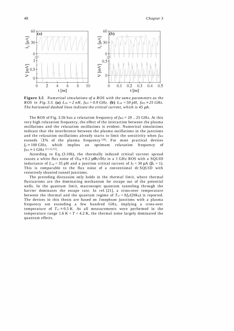
Chapter 348
The ROS of Fig. 3.5b has a relaxation frequency of fRO = 20 .. 25 GHz. At thisvery high relaxation frequency, the effect of the interaction between the plasmaoscillations and the relaxation oscillations is evident. Numerical simulationsindicate that the interference between the plasma oscillations in the junctionsand the relaxation oscillations already starts to limit the sensitivity when fRO
exceeds ∼1% of the plasma frequency [18]. For most practical devicesfp ≈ 100 GHz, which implies an optimum relaxation frequency offRO ≈ 1 GHz [11,12,15].
According to Eq. (3.10b), the thermally induced critical current spreadcauses a white flux noise of √SΦ ≈ 0.2 µΦ0/√Hz in a 1 GHz ROS with a SQUIDinductance of Lsq = 35 pH and a junction critical current of I0 = 30 µA (βL = 1).This is comparable to the flux noise of a conventional dc SQUID withresistively shunted tunnel junctions.
The preceding discussion only holds in the thermal limit, where thermalfluctuations are the dominating mechanism for escape out of the potentialwells. In the quantum limit, macroscopic quantum tunneling through thebarrier dominates the escape rate. In ref. [21], a cross-over temperaturebetween the thermal and the quantum regime of Tcr = hfp/(20kB) is reported.The devices in this thesis are based on Josephson junctions with a plasmafrequency not exceeding a few hundred GHz, implying a cross-overtemperature of Tcr ≈ 0.5 K. As all measurements were performed in thetemperature range 1.6 K < T < 4.2 K, the thermal noise largely dominated thequantum effects.
Figure 3.5 Numerical simulations of a ROS with the same parameters as theROS in Fig. 3.3. (a) Lsh = 2 nH, fRO = 0.9 GHz. (b) Lsh = 50 pH, fRO ≈ 25 GHz.The horizontal dashed lines indicate the critical current, which is 45 µA.

Relaxation Oscillation SQUIDs 49
3.2.2 Johnson noise
Besides the thermal fluctuations on the critical current, also the Johnson noisegenerated in the resistors Rsh and Rd affects the ultimate sensitivity of a ROS.The Johnson noise causes a noise current In,Rsh respectively In,Rd through thedc SQUID, which can cause premature switching from the superconducting tothe voltage state. In order to estimate the significance of the Johnson noise, themagnitude of the additional critical current spread due to In,Rsh and In,Rd shouldbe compared with the thermally induced spread ∆Ic, which, according toEq. (3.9), amounts to ∼1 µA for a ROS with a typical critical current ofIc = 2I0 = 60 µA.
The Johnson noise generated by Rsh is low pass filtered by the L-R circuitconstituted by Lsh and Rsh. Hence, the effective bandwidth of In,Rsh is of theorder of the relaxation frequency, leading to a root mean square (rms) value of
( )Ik TR
fn,RshB
shROrms ≈ ⋅
4. (3.12)
Substituting a typical value of Rsh = 2 Ω, Eq. (3.12) yields In,Rsh (rms) ≈ 0.3 µAfor a 1 GHz ROS operating at T = 4.2 K. This is well below the above-mentionedspread of about 1 µA due to thermal fluctuations. This example shows that inmost practical cases the Johnson noise generated by Rsh only has a minorcontribution to the overall noise.
As the Johnson noise generated by the damping resistor Rd is not filtered byan L-R circuit, its effective bandwidth is approximately the plasma frequency ofthe Josephson junctions, which implies an rms value of
( )Ik TR
fn,RdB
dprms ≈ ⋅
4(3.13)
for the Johnson noise originating from Rd. With typical values for fp and Rd
(100 GHz respectively 25 Ω), Eq. (3.19) yields In,Rd (rms) ≈ 1 µA, which is equalto the thermally induced critical current spread. This example indicates thatthermal noise from the damping resistor Rd can be a serious source of excessnoise.
Therefore, the design value for Rd should be a trade-off between acceptableJohnson noise - requiring a high resistance - and sufficient damping ofparasitic Lsh-Csq resonances - requiring a low resistance.

Chapter 350
3.3 Experimental ROS characteristics
3.3.1 ROS layout
In order to investigate the behaviour of ROSs operating at relaxationfrequencies in the GHz range, ROSs with Lsh/Rsh = 1 ns (1 GHz ROSs) andLsh/Rsh = 0.1 ns (10 GHz ROSs) were designed and fabricated by Adelerhof et al.at the Superconducting Sensor Laboratory [22] in Japan. The design parametersof these ROSs are listed in Table 3.1.
Figure 3.6 shows micrographs and schemes of the 1 GHz and the10 GHz ROS designs. The 2 x 2 µm2 Nb/Al,AlOx/Nb tunnel junctions, the otherNb structures and the SiO2 insulating layer were patterned with reactive ionetching in CF4. The resistors were structured in an Al thin film by wet chemicaletching in a NaOH solution. The junction critical current amounts to I0 ≈ 30 µAand the junction capacitance is estimated to be ∼0.25 pF per junction.
The inductance of the square Nb shunt inductor in the 1 GHz ROSs wascalculated with [23]
( )L aab
a bsh =
2 20π
µ ln » , (3.14)
with a and b as indicated in Fig. 3.6. For the 1 GHz ROSs, three differentvalues of Lsh were designed: 0.9 nH (a = 280 µm, b = 10 µm), 1.7 nH(a = 470 µm, b = 10 µm) and 3.0 nH (a = 750 µm, b = 10 µm).
The shunt inductance of the 10 GHz ROSs was designed symmetricallyaround the dc SQUID in order to avoid distortion of the ROS characteristicsdue to magnetic coupling between Lsh and the SQUID [24,25]. In thisconfiguration, Lsh was calculated as half the inductance of one of the twoparallel loops. The design values for Lsh in the 10 GHz ROSs were 0.16 nH(a = 150 µm, b = 20 µm) and 0.30 nH (a = 260 µm, b = 30 µm).
In order to keep the layout as symmetric as possible, the damping resistancewas distributed over two parallel meander-shaped resistors with a resistance of2Rd each. For the 1 GHz ROSs, three different values for the damping
Lsh= 3 nH Lsh= 1.7 nH Lsh= 0.9 nH Lsh= 0.3 nH Lsh= 0.16 nH
D Rsh Rd βC* Rsh Rd βC* Rsh Rd βC* Rsh Rd βC* Rsh Rd βC*
0.1 3 123 0.82 1.7 92 0.26 0.9 70 0.07 3 39 0.82 1.7 29 0.261 3 39 0.82 1.7 29 0.26 0.9 22 0.07 3 12.3 0.82 1.7 9.2 0.26
10 3 12.3 0.82 1.7 9.2 0.26 0.9 7 0.07 ... ... ... ... ... ...
Table 3.1 Design parameters of the investigated ROSs. The columns withLsh = 0.3 nH and Lsh = 0.16 nH represent the 10 GHz ROSs, in the othercolumns, the parameters of the 1 GHz ROSs are listed. (Rsh and Rd in Ω).

Relaxation Oscillation SQUIDs 51
parameter were designed: D = 10, 1 and 0.1. In the case of the 10 GHz ROS,only D = 1 and 0.1 were implemented. For D = 10, Rd should be ∼ 3 Ω, causingnon-hysteretic junction behaviour because βC < 1.
The washer-type hysteretic dc SQUIDs have a hole dimension of 13 µm andan outer width of 50 µm. The signal flux is applied by means of an integratedhalf-turn input coil. From the experimental critical current modulation depth,the SQUID inductance Lsq was determined to be 30 .. 35 pH (βL ≈ 1). This ismore than the expected value of 20 pH [from Eq. (2.19) ], which is probably dueto the small outer dimensions of the SQUID washers.
3.3.2 Characterization setup
A schematic diagram of the setup that was used for the characterization of theROSs is displayed in Fig. 3.7. The devices were cooled down in a stainless steel4He bath cryostat. To prevent disturbances due to external electromagneticnoise, the ROSs were enclosed by a superconducting niobium shield with alength of 19 cm and a diameter of 6 cm. For additional shielding, the entirecryostat was surrounded by a cylindrical µ-metal shield.
Figure 3.6 Micrographs and schemes of the ROSs which were used in theexperiments. In the 10 GHz ROS design, the meander-shaped damping resistorsare covered by a Nb film, electrically insulated from the resistors with a SiO2
layer.

Chapter 352
Four ROSs were glued on an epoxy printed circuit board (PCB) and cooleddown simultaneously. The electric contacts between the ROSs and the coppertransmission lines on the PCB were made by ultrasonic bonding of 25 µm thickAl wires with a length of approximately 5 mm. According to ref. [23], theparasitic inductance of these bonding wires is 10 to 20 nH. By means ofsubminiature A (SMA) connectors, the transmission lines on the PCB wereconnected to 50 Ω semi-rigid coaxial cables. Optionally, 50 Ω surface mounteddevice (SMD) resistors could be connected in series with the ROSs in order tostudy the effect of transmission line reflections.
The coaxial cables were used both to supply the dc bias current Ib to theROSs and to transfer the high frequency output signal from the ROSs to theroom temperature electronics. For this purpose, a bias tee (Mini-CircuitsZFBT-6G [26]) was used to split the ac and dc signals. After pre-amplificationwith a Hewlett Packard 83006A microwave system amplifier (gain ∼25 dB), thehigh frequency ROS output was coupled to a HP 8563E spectrum analyzer. Forground isolation, the home made bias current source was battery powered, andthe ground potential for the whole setup was determined by the spectrumanalyzer.
The time-averaged voltage <V> across the ROS was measured with a lownoise differential dc amplifier. As this is a two-point measurement, the rawreadout voltage had to be corrected for the resistance of the bias tee, the coaxialcable and the bonding wires, summing up to about 3.5 Ω.
The input coils of the ROSs were connected to a function generator bymeans of twisted manganin wires, shielded by a stainless steel tube. Thesewires were low pass filtered at the top of the cryostat in order to preventdegradation of the ROS characteristics due radio frequency interference(RFI) [27].
Figure 3.7 The ROS characterization setup.

Relaxation Oscillation SQUIDs 53
3.3.3 Voltage readout
In Fig. 3.8a, the experimental I-V characteristic of a 1 GHz ROS is shown.During the recording of this graph, the signal flux was swept with anamplitude of several Φ0 at a frequency considerably higher then the sweep rateof the bias current. Figure 3.8b shows the V-Φsig characteristics of the sameROS for 11 different bias currents. Both plots have been corrected for offsetvoltages due to the two-point measurement via the semi-rigid coaxial cable.
Figure 3.8a shows modulation for bias currents up to about 225 µA. Forlarger bias currents, the ROS does not oscillate anymore, as has been discussedin section 3.1.3. In this case, the voltage across the ROS is given byV = V∞ ≈ Ib⋅Rsh, which gives a direct method to determine the value of Rsh, asillustrated by the dashed line in Fig. 3.8a. Using Eq. (2.14), the SQUIDinductance of the devices was determined from the critical current modulationIc,max − Ic,min, as presented in the inset of Fig. 3.8a.
For large bias currents, the V-Φsig characteristics became irregular. For allROSs with D = 1, except those having Rsh ≈ 1 Ω, the bias current at which thefirst irregularities appeared was slightly larger than the theoretical maximumbias current as calculated with Eq. (3.4). Only for the ROSs with Rsh ≈ 1 Ω, theexperimental maximum bias current (∼150 µA) was smaller than the calculatedvalue of 225 µA. The maximum operation current was also dependent on thevalue of the damping parameter D. In general, the ROSs with D = 0.1 had asomewhat larger maximum bias current than their counterparts with D = 1.This is because the parasitic Lsh-Csq resonances can help to overcome the stable
Figure 3.8 (a) Ib-<V> characteristic of a 1 GHz ROS with design parametersLsh = 3 nH, Rsh = 3 Ω and D = 0.1. The inset shows a detailed view of the curvenear the origin. (b) <V>-Φsig characteristics of the same ROS for 11 differentbias currents, indicated at the right in µA.

Chapter 354
state in the subgap of the SQUID. Accordingly, the devices with D = 10 had aslightly smaller maximum bias current than those with D = 1.
The flux-to-voltage transfer of the V-Φsig traces in Fig. 3.8b isabout 200 µV/Φ0 for bias currents slightly above Ic,max. According to Eq. (2.16), acomparable non-hysteretic dc SQUID with junction shunt resistors of 3 Ω(βC = 0.2), has the same flux-to-voltage transfer. This is an experimentalconfirmation of the statement that ROSs are not particularly suited for voltagereadout. In literature, ROSs with much higher values for ∂V/∂Φsig have beenreported [15]. However, these high transfers originated mainly from parasiticmagnetic coupling between Lsh and the SQUID, causing an APF-likedeformation of the V-Φsig characteristics. From the horizontal shift of the V-Φsig
characteristics at different bias currents, the parasitic coupling between Lsh
and Lsq was determined to be only 1 .. 2 pH for the present 1 GHz ROSs. Due totheir symmetric layout, the 10 GHz ROSs showed an even smaller magneticcoupling between Lsh and the SQUID.
3.3.4 Frequency readout
In Fig. 3.9, the power spectral density S of the fundamental harmonic of acurrent biased 1 GHz ROS is shown for four different values of Φsig. The scaleof the vertical axis has not been corrected for the gain of the pre-amplifier(∼25 dB). The measured power level of the ground harmonic was typically 10 to20 dB below the theoretical value calculated with Eq. (3.5). Probably, this iscaused by transmission line losses; especially the connection between the ROSs
Figure 3.9 Spectra of the output voltage of the ROS of Fig. 3.8, measured at afixed bias current for four different values of Φsig. The vertical scale has not beencorrected for the gain of the pre-amplifier, which is about 25 dB.

Relaxation Oscillation SQUIDs 55
and the coaxial cables is not ideally suited for high frequencies due to theparasitic inductance of the bonding wires.
Due to the spectral impurity of the relaxation oscillation frequency, theoutput power is spread over a considerable bandwidth, often hundreds of MHz.In Fig. 3.9, this effect causes the peak width to increase and the peak height todecrease at higher relaxation frequencies. This behaviour is typical [25], and inpractice it often caused the output signal of the ROS to drown in the systemnoise at high relaxation oscillation frequencies. The experimental output powerwas smaller for ROSs with larger damping parameters D (i.e. small Rd), whichis to be expected as the damping resistor Rd decreases the amplitude of thevoltage pulses at the output. Similarly, the output power also decreased forROSs with a smaller shunt resistor Rsh. In the 1 GHz ROS with Rsh = 0.9 Ω andD = 10, both effects add, and consequently, the output power was too small fordetection with the present setup. The output of all 10 GHz ROSs was difficultto measure due to the high relaxation frequencies and the associated largetransmission line losses.
The shape of the peaks did not change qualitatively when a 50 Ω metal filmSMD resistor was connected between the ROSs and the coaxial cable, apartfrom a small reduction of the peak height. This indicates that the ROSdynamics is not severely influenced by the readout system. No clear relationcould be found between the spectral width of the peaks and the ROSparameters. Moreover, resonances, occurring either in the ROS or in thereadout system, caused the peak width to vary with the relaxation frequency.As a result, the output spectrum showed narrow peaks for certain combinationsof Ib and Φsig. However, at these points, the flux-to-frequency transfer ∂fRO/∂Φsig
was also rather low. Therefore, an estimation of the flux noise based on thespectral impurity of the relaxation oscillation signal, as given in ref. [28], isdoubtful.
Figure 3.10 shows the experimental fRO-Φsig characteristics of two different1 GHz ROSs. The characteristics were automatically recorded by a personalcomputer which was interfaced to the spectrum analyzer for frequencydetection and to an analogue-to-digital converter for measuring the signal flux.The βC* parameter of the ROS in Fig. 3.10b is smaller than that of the ROS inFig. 3.10a (design values 0.07 respectively 0.82). Therefore, the ROS inFig. 3.10b can operate at larger bias currents [see Eq. (3.4) ], and thus at higherrelaxation frequencies, than the ROS in Fig. 3.10a.
The solid lines in Fig. 3.10 are theoretical fits to the fRO-Φsig measurements.In these fits, fRO was calculated as 1/(T0+TV), with T0 from Eq. (3.3a) and withTV a constant fit parameter. The value of Lsh was also a fit parameter. All otherparameters were fixed: Lsq was determined from the critical currentmodulation, Rsh was derived from the I-V characteristic, and for Rd and Csq thedesign values were taken. The flux dependence of the critical current of thedc SQUID was calculated numerically [29], taking into account the magneticcoupling between Lsh and Lsq, which was determined from the V-Φsig
characteristics.

Chapter 356
Fits as shown in Fig. 3.10 have been made for all the characterized ROSs.For the 1 GHz ROSs, all configurations with the same design value for Lsh wereconfined to one common fit value for Lsh, whereas for the 10 GHz ROSs smalldifferences were permitted. The reason for allowing these small (< 3%)differences for the 10 GHz ROSs is that, due to the smaller dimensions of the
Figure 3.10 Experimental fRO-Φsig characteristics (markers) with theoreticalfits (solid lines) of two 1 GHz ROSs. All fit values are listed in Table 3.2.(a) ROS with a designed shunt inductance of Lsh = 3 nH, the value used for thetheoretical fits is 3.25 nH. The ROS was biased at four different bias currents:Ib = 45 µA (), Ib = 65 µA (), Ib = 75 µA () and Ib = 95 µA (~).(b) ROS with a designed shunt inductance of Lsh = 0.9 nH, the value used forthe theoretical fits is 0.95 nH. The ROS was biased at six different biascurrents: Ib = 55 µA (), Ib = 80 µA (), Ib = 100 µA (), Ib = 120 µA (~),Ib = 140 µA () and Ib = 170 µA (n).

Relaxation Oscillation SQUIDs 57
shunt inductor, the value of Lsh is rather sensitive to small variations in thefabrication process. The resulting fit values of TV and Lsh are listed in Table 3.2.If TV and Lsh were changed by 10%, the fRO-Φsig fits clearly worsened. Thissuggests that the fit accuracy is better than 10%. The good correspondencebetween the fit and design values of Lsh is obvious. The fit values for TV are alsoplausible as they are of the order of π√(LshCsq), as was to be expected fromEq. (3.3b). The maximum observed relaxation frequency fRO,max and themaximum critical current Ic,max are also tabulated for each ROS in Table 3.2.
3.3.5 Flux locked loop operation
For flux locked loop (FLL) operation, the output signal of the ROS has to be FMdemodulated. For relaxation frequencies below a few hundred MHz, thisfrequency-to-voltage conversion can be implemented with standard radioelectronics [30,31]. For relaxation frequencies in the GHz range, however, theFM demodulation is not straightforward, especially when the center frequencyof the demodulator should be adjustable over a range of several GHz.
D Lsh
[nH]Rsh
[Ω]TV
[ps]Ic,max
[µA]fRO,max
[GHz]
Design Design Fit Meas. Fit Meas. Meas.
0.1 d) 3 3.25 3.0 133 61 2.61 b) 3 3.25 2.8 120 59 1.410 3 3.25 2.5 113 53 1.4
0.1 1.7 1.70 2.0 169 69 2.61 1.7 1.70 1.6 141 57 1.810 1.7 1.70 2.0 173 56 1.7
0.1 c) 0.9 0.95 2.0 96 61 5.01 0.9 0.95 1.6 125 70 2.110 0.9 a) 1.5 a) 62 a)
0.1 0.3 0.35 2.0 50 66 6.81 0.3 0.34 1.6 39 72 5.6
0.1 0.16 0.19 1.0 26 71 5.61 0.16 0.19 1.1 35 71 5.8
a) Output signal too weak for fRO-Φsig measurements.b) fRO-Φsig fit is shown in Fig. 3.10a.c) fRO-Φsig fit is shown in Fig. 3.10b.d) characteristics are shown in Figs. 3.8, 3.9 and 3.12.
Table 3.2 Measured and designed ROS parameters. For each ROS, themaximum observed relaxation frequency is indicated in the last column.
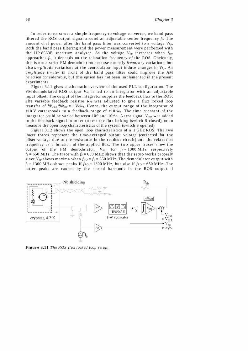
Chapter 358
In order to construct a simple frequency-to-voltage converter, we band passfiltered the ROS output signal around an adjustable center frequency fc. Theamount of rf power after the band pass filter was converted to a voltage Vbp.Both the band pass filtering and the power measurement were performed withthe HP 8563E spectrum analyzer. As the voltage Vbp increases when fRO
approaches fc, it depends on the relaxation frequency of the ROS. Obviously,this is not a strict FM demodulation because not only frequency variations, butalso amplitude variations at the demodulator input induce changes in Vbp. Anamplitude limiter in front of the band pass filter could improve the AMrejection considerably, but this option has not been implemented in the presentexperiments.
Figure 3.11 gives a schematic overview of the used FLL configuration. TheFM demodulated ROS output Vbp is fed to an integrator with an adjustableinput offset. The output of the integrator supplies the feedback flux to the ROS.The variable feedback resistor Rfb was adjusted to give a flux locked looptransfer of ∂VFLL/∂Φsig = 1 V/Φ0. Hence, the output range of the integrator of±10 V corresponds to a feedback range of ±10 Φ0. The time constant of theintegrator could be varied between 10-9 and 10-4 s. A test signal Vtest was addedto the feedback signal in order to test the flux locking (switch S closed), or tomeasure the open loop characteristics of the system (switch S opened).
Figure 3.12 shows the open loop characteristics of a 1 GHz ROS. The twolower traces represent the time-averaged output voltage (corrected for theoffset voltage due to the resistance in the readout circuit) and the relaxationfrequency as a function of the applied flux. The two upper traces show theoutput of the FM demodulator, Vbp, for fc = 1300 MHz respectivelyfc = 650 MHz. The trace with fc = 650 MHz shows that the setup works properlysince Vbp shows maxima when fRO = fc = 650 MHz. The demodulator output withfc = 1300 MHz shows peaks if fRO = 1300 MHz, but also if fRO = 650 MHz. Thelatter peaks are caused by the second harmonic in the ROS output if
Figure 3.11 The ROS flux locked loop setup.

Relaxation Oscillation SQUIDs 59
fRO = 650 MHz. Since this peak is more pronounced than the peak caused by theoscillation at fRO = 1300 MHz, flux locking at fRO = 1300 MHz is not stable asthe system easily unlocks and relocks to the second harmonic of thefRO = 650 MHz oscillation. Generally, for a given bias current, optimum FLLperformance was obtained for fc slightly larger than the minimum relaxationfrequency at that bias current.
All ROSs were operated in the FLL setup of Fig. 3.11. Stable flux locking atrelaxation frequencies in the GHz range was achieved for all of them. Thebandwidth of the FLL was more than 100 kHz. The flux noise was determinedby probing the FLL output with a HP 3562A FFT spectrum analyzer. The1 GHz ROS with Lsh = 3 nH, Rsh = 3 Ω and D = 0.1, i.e. the ROS with the largesthigh frequency output power, had the best white flux noise, √SΦ ≈ 2.5 µΦ0/√Hzat a locking frequency of fc = 2.15 GHz. This flux noise corresponds to an energysensitivity of ε = SΦ/2Lsq ≈ 600 h. Generally, ROSs with a smaller output powershowed higher flux noise levels. Therefore, the 10 GHz ROSs, whichtheoretically have a better sensitivity, but also a weaker output signal, had ahigher flux noise than the 1 GHz ROSs. The best measured white flux noise for
Figure 3.12 <V>, fRO, Vbp(fc=650MHz) and Vbp(fc=1300MHz) as function of theapplied signal flux Φsig in open loop configuration for the ROS marked with d) inTable 3.2. The bias current of the ROS was 75 µA.

Chapter 360
a 10 GHz ROS operated in FLL was √SΦ ≈ 4 µΦ0/√Hz (ε ≈ 1500 h) at fc = 5 GHz.In all cases, the 1/f corner frequency was below 10 Hz.
3.4 Discussion and conclusions
The operation of a ROS as a flux-to-frequency converter is described very wellby the model presented in section 3.1, which is demonstrated by the fRO-Φsig fitsin Fig. 3.10. The model was verified for relaxation frequencies up to 7 GHz,higher relaxation frequencies could not be detected due to transmission linelosses. For all characterized devices, the fit values for Lsh were very close to thedesign values.
The voltage readout measurements in section 3.3.3 show that, as expected,the typical flux-to-voltage transfer coefficient of a ROS equals that of aresistively shunted non-hysteretic dc SQUID. Therefore, voltage readout of aROS has no significant advantages in comparison with the conventionaldc SQUID readout scheme. This is confirmed by measurements reported in theliterature. In ref. [15], for instance, 100 MHz ROSs were operated in a non-modulated FLL with direct voltage readout. The best observed energyresolution was ε ≈ 1500 h. Reference [32] reports a resolution of around 600 hfor a 1 GHz ROS, operated with voltage readout in a flux modulated FLL.These noise levels are significantly above those of non-hysteretic dc SQUIDs.
In section 3.3.5, a FLL based on frequency readout in the GHz range waspresented. The best obtained energy sensitivity of ε ≈ 600 h is better than thesensitivity of 2500 .. 3000 h which has previously been reported in theliterature for a flux locked 10 MHz ROS [30]. However, it exceeds the theoreticalsensitivity given by Eq. (3.10b) by more than two orders of magnitude. Thereare two indications that the surplus noise originates mainly from the non-idealFM demodulator that was used. First, DROSs with an analogous layout showedintrinsic energy resolutions as low as 13 h [33,34], which is close to the theoreticalexpectation (see chapter 4). Second, a correlation was observed between theoutput power of the ROSs and the noise performance. This suggests thatspurious AM components in the output signal of the ROS cause significantfluctuations at the output of the frequency-to-voltage converter.
A cryogenic high electron mobility transistor (HEMT) high frequency pre-amplifier, as used for the readout of contemporary rf SQUIDs [35], couldimprove the sensitivity significantly. Another advantage of this configurationwould be the decoupling of the ROS and the coaxial transmission line, whichprevents degradation of the ROS characteristics due to transmission lineresonances. However, such a cryogenic pre-amplifier would increase thecomplexity of the system. Moreover, the number of wires from roomtemperature to the cryogenic environment would be increased, as is the powerdissipation at 4.2 K. This is in contradiction with the primary aim of the workin this thesis, which is to reduce the complexity of dc SQUID systems.
Relaxation Oscillation SQUIDs 61
The need for high frequency transmission lines between the ROS and theelectronics at room temperature is another drawback in comparison with othersecond generation dc SQUID systems, e.g. the dc SQUID array, the dc SQUIDwith APF or the DROS. These schemes can be operated with simple twistedwires for readout. In a multi-channel ROS system, the number of coaxial cablescould be reduced by connecting several ROSs in series, each ROS being fluxlocked at a different relaxation frequency. However, in this configuration, themaximum number of ROSs per transmission line is still limited because theoutput signals of the different ROSs should not overlap in the frequencydomain. Moreover, if one ROS unlocks, its output frequency is not determinedanymore, and therefore it can also cause the other ROSs to unlock.
References1 M. Klein and A. Mukherjee, “Thermal noise induced switching of Josephson logic devices”,
Appl. Phys. Lett. 40, 744-747 (1982).2 Simulation software: JSIM 2.1, developed by E.S. Fang, University of California, Berkeley,
CA 94720, U.S.A.3 T.A. Fulton, “Punchthrough and the tunneling cryotron”, Appl. Phys. Lett. 19, 311-313
(1971).4 T.A. Fulton and R.C. Dynes, “Switching to zero voltage in Josephson tunnel junctions”,
Solid State Comm. 9, 1069-1073 (1971).5 M.J. van Duuren, D.J. Adelerhof, G.C.S. Brons, J. Kawai, G. Uehara, H. Kado, J. Flokstra
and H. Rogalla, “Frequency readout of relaxation oscillation superconducting quantuminterference devices in the GHz regime”, J. Appl. Phys. 80, 4164-4173 (1996).
6 A.D. Smith, R.D. Sandell, A.H. Silver and J.F. Burch, “Chaos and bifurcation in Josephsonvoltage-controlled oscillators”, IEEE Trans. Magn. 23, 1267-1270 (1987).
7 J. Clarke, “SQUID fundamentals”, in SQUID Sensors: Fundamentals, Fabrication andApplications, ed. H. Weinstock, NATO ASI Series 329, Kluwer Academic Publishers,Dordrecht / Boston / London (1996).
8 T.A. Fulton and L.N. Dunkleberger, “Lifetime of the zero-voltage state in Josephson tunneljunctions”, Phys. Rev. B 9, 4760-4768 (1974).
9 D.J. Adelerhof, Second generation dc SQUID magnetometers: (Double) RelaxationOscillation SQUIDs, Ph.D. thesis University of Twente, Enschede (1993).
10 J. Kadlec, “Noise margins for Josephson logic and memory devices”, IEEE Trans. Magn. 19,1213-1216 (1983).
11 N. Fujimaki, H. Tamura, T. Imamura and S. Hasuo, “Thermal noise-limited sensitivity ofthe pulse-biased SQUID magnetometer”, J. Appl. Phys. 65, 1626-1630 (1989).
12 O.V. Snigirev, “Ultimate sensitivity of the dc SQUIDs using unshunted Josephson tunneljunctions”, IEEE Trans. Magn. 19, 584-586 (1983).
13 J.D. Feder, M. Klein and C.J. Anderson, “Thermal noise in Josephson devices”, IEEE Trans.Appl. Supercond. 3, 2760-2764 (1993).
14 D.J. Adelerhof, J. Flokstra and H. Rogalla, “Noise in (double) relaxation oscillationSQUIDs”, Physica B 194-196, 141-142 (1994).
15 D.J. Adelerhof, H. Nijstad, J. Flokstra and H. Rogalla, “(Double) relaxation oscillationSQUIDs with high flux-to-voltage-transfer: Simulations and experiments”, J. Appl. Phys.76, 3875-3886 (1994).

Chapter 362
16 J. Kurkijärvi, “Intrinsic fluctuations in a superconducting ring closed with a Josephsonjunction”, Phys. Rev. B 6, 832-835 (1972).
17 S.A. Gugoshnikov, O.V. Kaplunenko, Y.V. Maslennikov and O.V. Snigirev, “Noise inrelaxation-oscillation driven SQUIDs”, IEEE Trans. Magn. 27, 2439-2441 (1991).
18 D.J. Adelerhof, M.J. van Duuren, J. Flokstra and H. Rogalla, “High sensitivity magneticflux sensors with direct voltage readout: Double relaxation oscillation SQUIDs”, IEEETrans. Appl. Supercond. 5, 2160-2163 (1995).
19 C.B. Whan and C.J. Lobb, “Complex dynamical behaviour in RCL-shunted Josephsonjunctions”, IEEE Trans. Appl. Supercond. 5, 3094-3097 (1995).
20 P.M. Marcus, Y. Imry and E. Ben-Jacob, “Characteristic modes and the transition to chaosof a resonant Josephson circuit”, Solid State Comm. 41, 161-166 (1982).
21 L.D. Jackel, J.P. Gordon, E.L. Hu, R.E. Howard, L.A. Fetter, D.M. Tennant, R.W. Epworthand J. Kurkijärvi, “Decay of the zero-voltage state in small-area, high-current-densityJosephson junctions”, Phys. Rev. Lett. 47, 697-700 (1981).
22 Superconducting Sensor Laboratory, 2-1200 Muzaigakuendai Inzai, Chiba 270-13, Japan.23 F.W. Grover, Inductance calculations, working formulas and tables, Dover Publications Inc.,
New York (1962).24 D.J. Adelerhof, M.J. van Duuren, J. Flokstra and H. Rogalla, “Second generation dc SQUID
sensors: ROS with frequency readout and DROS with voltage readout”, in SuperconductiveDevices and Circuits, ed. R.A. Buhrman, J. Clarke, K. Daly, R.H. Koch, J.A. Luine and R.W.Simon, proc. SPIE 2160, 142-153 (1994).
25 J. Kawai, G. Uehara and H. Kado, “The effects of the self-magnetic fields in relaxationoscillation SQUIDs”, in Superconductive Devices and Circuits, eds. R.A. Buhrman, J.Clarke, K. Daly, R.H. Koch, J.A. Luine and R.W. Simon, proc. SPIE 2160, 154-162 (1994).
26 Mini-Circuits, P.O. Box 350166, Brooklyn, NY 11235, U.S.A.27 R.H. Koch, V. Foglietti, J.R. Rozen, K.G. Stawiasz, M.B. Ketchen, D.K. Lathrop, J.Z. Sun
and W.J. Gallagher, “Effects of radio frequency radiation on the dc SQUID”, Appl. Phys.Lett. 65, 100-102 (1994).
28 G. Uehara, T. Morooka, J. Kawai, N. Mizutani and H. Kado, “Characteristics of therelaxation oscillating SQUID with tunnel junctions”, IEEE Trans. Appl. Supercond. 3,1866-1869 (1993).
29 R.L. Peterson and C.A. Hamilton, “Analysis of threshold curves for superconductinginterferometers”, J. Appl. Phys. 50, 8135-8142 (1979).
30 M. Mück and C. Heiden, “Simple dc SQUID system based on a frequency modulatedrelaxation oscillator”, IEEE Trans. Appl. Magn. 25, 1151-1153 (1989).
31 M. Mück, H. Rogalla and C. Heiden, “A frequency-modulated read-out system fordc SQUIDs”, Appl. Phys. A 47, 285-289 (1988).
32 S.A. Gudoshnikov, Yu.V. Maslennikov, V.K. Semenov, O.V. Snigirev and A.V. Vasiliev,“Relaxation-oscillation-driven dc SQUIDs”, IEEE Trans. Magn. 25, 1178-1181 (1989).
33 D.J. Adelerhof, J. Kawai, G. Uehara and H. Kado, “High sensitivity double relaxationoscillation superconducting quantum interference devices”, Appl. Phys. Lett. 65, 2606-2608(1994).
34 D.J. Adelerhof, J. Kawai, G. Uehara and H. Kado, “High sensitivity double relaxationoscillation superconducting quantum interference devices with large transfer from flux tovoltage”, Rev. Sci. Instrum. 66, 2631-2637 (1995).
35 G. Fontana, R. Mezzena, S. Vitale, M. Cerdonio, M. Mück, G. Hallmanns and C. Heiden,“Improved sensitivity of planar microwave biased rf SQUIDs using a cryogenic HEMTpreamplifier”, IEEE Trans. Appl. Supercond. 3, 1820-1823 (1993).

63
Chapter 4
Double Relaxation Oscillation SQUIDs
Unlike the relaxation oscillation SQUID (ROS), the double relaxationoscillation SQUID (DROS) is used with voltage readout instead of frequencyreadout. Therefore, simple twisted wires can be used for its readout, as opposedto the coaxial transmission lines which are required for the readout of a ROS.The large flux-to-voltage transfer of a DROS, typically ∂V/∂Φsig = 1 mV/Φ0,enables direct voltage detection with a room temperature dc amplifier withoutdegradation of the sensitivity. Thus, flux modulation techniques and resonantimpedance matching circuitry are not required and the flux locked loopelectronics can be simple and compact, which is an important feature,especially in multi-channel SQUID systems. Moreover, wide bandwidthoperation is easier to accomplish with a non-modulated readout scheme and thecrosstalk between adjacent channels is also reduced.
The principle of operation of the DROS has already been treated roughly insection 2.5.4. A more thorough discussion will be given in section 4.1. Like forROSs, the optimum relaxation frequency for DROSs is also in the lower GHzrange. As has been confirmed experimentally [1,2], the sensitivity of a DROSwith this relaxation frequency is of the same order as that of a comparable non-hysteretic dc SQUID with resistively shunted tunnel junctions.
To demonstrate the practical applicability of DROSs, we constructed anumber of DROS-based measuring systems, which will be presented in thischapter. First, in section 4.2, a three-channel DROS gradiometer with wire-wound pickup coils will be discussed. Operated inside a superconductingshielding, this first-order gradiometer system had a white magnetic field noiseof √SB = 4 fT/√Hz (10 fT/√Hz @ 1 Hz) [3]. For comparison, a magnetic field noiselevel of 10 fT/√Hz in a frequency band between 1 Hz and 1 kHz is generallyconsidered to be sufficient for bio-magnetic measurements, such as magneto-encephalography (MEG) [4]. Next, in section 4.3, a DROS with a gradiometric

Chapter 464
signal SQUID will be presented. Connected to an external planar first-ordergradiometer, this device had a magnetic field sensitivity better than 2 fT/√Hz(∼10 fT/√Hz @ 1 Hz) inside a magnetically shielded room [5]. The third exampleof a practical DROS system is the 8 x 8 mm2 directly coupled multi-loop DROSmagnetometer which is discussed in section 4.4. Unlike the systems presentedin sections 4.2 and 4.3, this device did not require an external superconductingflux transformer to enlarge its effective pickup area. Inside a superconductingshielding, the white magnetic field noise of the directly coupled DROS was7 fT/√Hz [6].
In section 4.5, a DROS is used as a current sensor with a sensitivity betterthan 2 pA/√Hz. To demonstrate this sensitivity, the subgap I-V characteristic ofa voltage biased Nb/Al,AlOx/Al/Nb tunnel junction was measured. This type ofmeasurement is for instance of relevance for the readout of X-rayspectrometers based on superconducting tunnel junctions or hot electronbolometers. In section 4.6, the results of this chapter are summarized.
4.1 Operation theory of the DROS
A DROS consists of two hysteretic dc SQUIDs in series, shunted by an inductorLsh and a resistor Rsh, as shown in the scheme of Fig. 4.1a. If the device isbiased with an appropriate dc bias current Ib, relaxation oscillations aregenerated according to the same conditions which hold for a ROS, cf. Eq. (3.4).
Figure 4.1 (a) Schematic representation of a DROS. (b) Schematic Ic-Φsig and<V>-Φsig characteristics of a DROS. The shaded region around the Ic-Φsig tracesrepresents the thermal critical current noise of both hysteretic dc SQUIDs.

Double Relaxation Oscillation SQUIDs 65
As for a ROS, parasitic resonances in the L-C-R circuit constituted by theshunt inductor (Lsh), the capacitance of the SQUIDs (Csq) and the shunt resistor(Rsh) can be suppressed with an optional damping resistor Rd. For adequatedamping of the Lsh-Csq resonances, the resistor Rd should be dimensioned suchthat the damping parameter D, defined in Eq. (3.1), is larger than unity.
The signal flux Φsig is applied to the upper SQUID, the signal SQUID,whereas a constant reference flux Φref is used to adjust the critical current ofthe other SQUID, the reference SQUID, to a value in the middle of the criticalcurrent modulation range of the signal SQUID. This is indicated in theschematic Ic-Φsig plot of Fig. 4.1b.
Basically, in each relaxation oscillation cycle, the critical currents of the twohysteretic dc SQUIDs are compared. If Ic,sig(Φsig) < Ic,ref, only the signal SQUIDparticipates in the relaxation oscillations and the reference SQUID remainssuperconducting. Consequently, in this situation, the output voltage of theDROS, which is measured across the reference SQUID, is equal to zero. On theother hand, for values of the signal flux giving Ic,sig(Φsig) > Ic,ref, only thereference SQUID oscillates, and the DROS output consists of voltage pulses atthe relaxation frequency. Since the bandwidth of the readout amplifier issmaller than the relaxation frequency typically by a few orders of magnitude,the pulsed nature of the output voltage is not observed, and only the time-averaged voltage <V> is measured. Thus, depending on the value of Φsig, thetime-averaged DROS output equals either zero or has a certain value, labeledVc. The transition between these two states at Ic,sig(Φsig) = Ic,ref is very sharp,resulting in a large flux-to-voltage transfer, as illustrated by the schematic<V>-Φsig characteristic in Fig. 4.1b.
4.1.1 Voltage modulation depth
The theoretical maximum bias current Ib,max at which a DROS still operatescorrectly can be determined from the operation criterion of Eq. (3.4),substituting Ic = 2I0:
II
RI
C
I R Cb,max
Csh sq
Csh sq= = ⋅ =
⋅ ⋅ ⋅2 1 2 20 0 0 0
2
0β πβ
π*
*withΦ
Φ. (4.1)
In Eq. (4.1), I0 represents the critical current of one Josephson junction and Csq
is the SQUID capacitance. To ensure proper operation, βC* is designed muchsmaller than unity in most practical DROSs. Hence, in practice, Ib,max » 2I0.This is in contrast with conventional dc SQUIDs, which are generally biased ata bias current slightly above 2I0.
If the reference SQUID oscillates, the time-averaged output voltage of theDROS equals that of a ROS with identical parameters. The ROS I-Vcharacteristic of Fig. 3.8a shows that <V> approaches Ib⋅Rsh for Ib » 2I0. Forsmaller bias currents, <V> is somewhat below this asymptotic value, and at

Chapter 466
Ib ≈ Ib,max, <V> = (0.5 .. 0.75)⋅Ib⋅Rsh [2]. Combined with Eq. (4.1), this yields thefollowing expression for the theoretical maximum output voltage swing of aDROS:
( ) ( )V I RI
Cc,max b,max shsq
= ⋅ ⋅ = ⋅0 5 075 0 5 075 0 0. .. . . .. .Φ
π. (4.2)
Equation (4.2) shows that the modulation depth of the V-Φsig characteristicdoes not depend on the signal SQUID inductance, at least when noise effectsare not taken into consideration.
4.1.2 Flux-to-voltage transfer
At 4.2 K, where the thermal limit applies, the flux-to-voltage transfer of a welldamped DROS is limited by the thermally induced critical current spread ofboth SQUIDs. In Fig. 4.1b, this spread is symbolized by the shaded regionaround the traces. Assuming a linear transition between <V> = 0 and <V> = Vc,the flux-to-voltage transfer is given by
∂∂Φ
V V
sig
c=∆Φ
, (4.3a)
where ∆Φ represents the width of the transition, as indicated in Fig. 4.1b. Thetransition width ∆Φ is related to the spread in the critical currents via
( )∆Φ∆ ∆
=+I I
Ic,ref c,sig
c,sig sig∂ ∂Φ, (4.3b)
where ∆Ic,ref and ∆Ic,sig are the thermal spreads of the critical currents of thereference SQUID respectively the signal SQUID. Evaluating these spreadswith the single junction approximation, by substituting a critical current of 2I0
in Eq. (3.9), Eq. (4.3a) can be rewritten as
( )∂
∂Φ β αV
gI V
gsig L,sig
c= ⋅+
⋅ ≈ = ⋅ −02 3
0
4 2 3
1
177 10 4 2
Φ,
.A @ . K , (4.3c)
where Eq. (3.11) has been used to calculate ∂Ic,sig/∂Φsig. The parameter α waspreviously introduced in Eq. (3.9) and has a T2/3 temperature dependence.Therefore, the parameter g in Eq. (4.3c) varies as T-2/3 with temperature.
Thus, at T = 4.2 K, a DROS with I0 = 10 µA, βL,sig = 1 and a SQUIDcapacitance of 1 pF theoretically has an output voltage swing of ∼50 µV[from Eq. (4.2) ] and a flux-to-voltage transfer of approximately 800 µV/Φ0
[from Eq. (4.3c) ]. For comparison, a non-hysteretic dc SQUID with the same

Double Relaxation Oscillation SQUIDs 67
critical current and inductance, having junction shunt resistors of 4 Ω(βC = 0.25), has a flux-to-voltage transfer coefficient of only ∼80 µV/Φ0,according to Eq. (2.16).
For some DROSs, we experimentally observed a degradation of the flux-to-voltage transfer due to the Johnson noise of Rd [6]. The magnitude of thisreduction of ∂V/∂Φsig depends on the exact layout of the damping circuit. As anexample, Fig. 4.2 shows two possible configurations. In Fig. 4.2a, one dampingresistor shunts both SQUIDs, and in Fig. 4.2b, each SQUID is shunted by aseparate damping resistor.
In the configuration of Fig. 4.2a, the Johnson noise generated in Rd flowsthrough both SQUIDs, and consequently the additional noise currents throughboth SQUIDs are correlated. Therefore, the relative switching probabilities ofthe SQUIDs are hardly influenced and a severe degradation of ∂V/∂Φsig is notlikely. In the configuration of Fig. 4.2b, however, the Johnson noise currentsthrough both SQUIDs are not correlated. This results in an additional spread ofthe critical currents of both SQUIDs, superimposed on the thermal spread.According to Eqs. (4.3a) and (4.3b), this increased critical current spreaddecreases the flux-to-voltage transfer ∂V/∂Φsig. In section 4.4.2, this negativeside effect of the damping resistors will be discussed in more detail.
4.1.3 Sensitivity
The maximum flux-to-voltage transfer is obtained at those values of Φsig wherethe critical currents of the reference SQUID and of the signal SQUID are equal.At these points, both SQUIDs have a switching probability of 50% in eachrelaxation cycle. Consequently, the average voltage over a time span ∆t » 1/fRO
is ½Vc, with a standard deviation of ½Vc/√(fRO⋅∆t). For frequencies much lowerthan the relaxation frequency, this implies a voltage noise at the DROS outputof
Figure 4.2 Two possible damping configurations for a DROS.

Chapter 468
SVfV
c
RO=
2
4. (4.4a)
From Eqs. (4.4a) and (4.3c), the equivalent flux noise can be calculated:
( )( )
SS
V f I
g
V
sig
dros
L,sig
RO
dros
Φ
Φ= ≈ ⋅
+ ⋅
⋅
= ≈ ⋅ −
∂ ∂Φχ
β
χ
2
2
02
04 3
211 4 3
1
1
451 10 4 2
,
. A @ . K .
(4.4b)
As g ∝ T-2/3, Eq. (4.4b) implies that, according to the present model, the fluxnoise SΦ of a DROS scales with temperature as T4/3. This is close to the T6/5
temperature dependence which was derived analytically in ref. [7].Equation (4.4b) shows a strong analogy with Eq. (3.10b), expressing the
sensitivity of a ROS. As for a ROS, the sensitivity of a DROS also improves athigher relaxation frequencies. However, the sensitivity can not be improvedinfinitely by taking increasingly higher values for the relaxation frequency.Numerical simulations show that the flux-to-voltage transfer decreases belowthe thermally limited value of Eq. (4.3c) when fRO exceeds a few percent of theplasma frequency of the junctions [8], which impedes a further reduction of theflux noise level. With a typical plasma frequency of 100 GHz, the optimumrelaxation frequency is therefore about 1 GHz for most practical DROSs.According to Eq. (4.4b), at T = 4.2 K, a DROS with fRO = 1 GHz, βL,sig = 1 andI0 = 10 µA has a thermally limited flux noise of √SΦ = 1 µΦ0/√Hz (ε = 30 h).
The sensitivity of a DROS is also influenced by the Johnson noise generatedby the resistors Rsh and Rd. As was discussed in section 4.1.2, the Johnson noisefrom the damping resistance Rd may decrease the flux-to-voltage transfer. AsEq. (4.4b) implies that the flux noise spectral density is inversely proportionalto (∂V/∂Φsig)2, this reduction of the transfer function of the DROS directlyresults in a worse sensitivity.
The Johnson noise of Rsh causes a voltage noise of SV = (4kBT/Rsh)⋅Rdyn2 atthe output, with Rdyn the dynamic resistance ∂V/∂Ib of the DROS. Using theapproximation Rdyn ≈ Rsh, a shunt resistor with a typical value of Rsh = 1 Ωcontributes to the output voltage noise by an amount of only 15 pV/√Hz. This ismuch less than the contribution of other noise sources, such as the inputvoltage noise of the pre-amplifier, which is of the order of 1 nV/√Hz. From thisexample, one can conclude that the Johnson noise generated by Rsh is not amajor noise source in a DROS. Furthermore, the Johnson noise of Rsh is lowpass filtered by the L-R circuit constituted by Lsh and Rsh, which preventsdegradation of the DROS performance due to downmixing with the Josephsonoscillations in the junctions.

Double Relaxation Oscillation SQUIDs 69
4.1.4 Experimental verification
In order to verify the theory discussed in the previous sections, Adelerhof etal. [1,2] have fabricated and characterized DROSs with various parameters atthe Superconducting Sensor Laboratory in Japan [9]. In this section, their mainresults are summarized.
The layout and design parameters of the DROSs were equivalent to the1 GHz and 10 GHz ROSs presented and discussed in chapter 3. Like theseROSs, they did not have multi-turn input coils, and the signal flux was appliedby means of a half-turn input coil. The average experimental ∂V/∂Φsig of thenine characterized 1 GHz DROSs was 4.2 mV/Φ0 (standard deviation:1.1 mV/Φ0), which is close to the theoretical value of ∼5 mV/Φ0 [from Eqs. (4.3c)and (4.2) ]. The flux-to-voltage transfer of the 10 GHz DROSs was somewhatsmaller: 2.6 mV/Φ0 on the average. This is probably caused by the interactionbetween the relaxation oscillations and the plasma oscillations at elevatedrelaxation frequencies.
For the 1 GHz DROSs, the value of the damping parameter D had a clearinfluence on the sensitivity. Generally, the energy resolution improved by afactor of 2 to 3 when D was increased from 0.1 to 10. This clearly indicates thepositive effect of damping of the Lsh-Csq resonances. For the 10 GHz DROSs,however, the amount of damping did not change the sensitivity significantly.This is another indication that the sensitivity of the 10 GHz devices is limitedby interference of the plasma oscillations and the relaxation oscillations.
Figure 4.3 Theoretical (solid line) and experimental (markers) intrinsicenergy sensitivity of 1 GHz and 10 GHz DROSs versus the calculated relaxationfrequency. Data from ref. [2].
Chapter 470
Figure 4.3 shows the intrinsic energy resolution εintr of three 1 GHz DROSsand three 10 GHz DROSs as a function of the calculated relaxation frequencyfRO [2]. The intrinsic noise was measured in open loop, subtracting the pre-amplifier noise. The solid line in Fig. 4.3 was calculated with Eq. (4.4b). Forrelaxation frequencies below approximately 2 GHz, the difference betweentheory and experiment is only about 10 h. At higher relaxation frequencies, themeasured sensitivity levels off at 13 .. 14 h. These results show that the theoryin the previous sections is reasonably accurate as long as the relaxationfrequency does not exceed ∼1% of the plasma frequency.
Due to the noise of the room-temperature amplifier (1.5 nV/√Hz in the whiteregion), the energy sensitivity of the DROSs in flux locked loop (FLL) wasworse than the intrinsic sensitivities depicted in Fig. 4.3. The best measuredenergy resolution in FLL was 34 h, at fRO = 1 .. 2 GHz.
As already mentioned, the DROSs used in these experiments had no tightlycoupled multi-turn input coils. In the next sections, some DROS designs withmulti-turn input coils will be discussed.
4.2 A three-channel DROS gradiometer
In this section, the construction and operation of a three-channel DROS first-order gradiometer system with wire-wound pickup coils is discussed. TheDROSs in this system are identical to those used in a single-channel planargradiometer system that was constructed by Adelerhof et al. [10] at theSuperconducting Sensor Laboratory. With that system, which had a whitemagnetic field sensitivity of √SB = 5 fT/√Hz, magneto-encephalograms (MEG) ofauditory evoked responses were measured in a magnetically shielded room.This proves the applicability of DROSs for bio-magnetic measurements.However, the results obtained with this single-channel system do not makeclear whether interference between relaxation oscillations in adjacent DROSs,caused by crosstalk via the flux transformers, could lead to a degradation of thesensitivity in multi-channel DROS magnetometer systems. The three-channelgradiometer system which is discussed here was primarily constructed toexamine this aspect of multi-channel DROS magnetometry.
4.2.1 DROS layout
A micrograph and the corresponding circuit of the DROSs are shown inFig. 4.4. The Nb/Al,AlOx/Nb Josephson tunnel junctions, the Nb structures andthe SiO2 insulating layer were patterned by reactive ion etching in a CF4
plasma. The Al resistors were defined by wet chemical etching in a NaOHsolution.
The size of the hole in the signal SQUID washer is 100 µm, whichcorresponds to an inductance of ∼160 pH according to Eq. (2.19). The actualSQUID inductance, determined from the experimental critical currentmodulation depth, was Lsq,sig = 240 pH. It is realistic to attribute the difference

Double Relaxation Oscillation SQUIDs 71
of 80 pH to the parasitic inductance of the double 2-µm-wide and 250-µm-longslit in the washer [11]. The 25-turns input coil on top of the signal SQUID has adesigned inductance of Lin = 100 nH [from Eq. (2.20a) ]. The experimentallydetermined mutual inductance between the input coil and the signal SQUID isMin = 4.1 nH. This corresponds to a coupling coefficient ofk = Min/√(Lsq⋅Lin) = 0.84, if the design value of 100 nH is substituted for Lin. Themutual inductance between Lsq and the single-turn feedback coil at the edge ofthe washer was measured to be Mfb = 220 pH. The 2 x 2 µm2 Josephsonjunctions, located at the outer side of the washer, have a critical current ofI0 = 5.5 µA and an estimated capacitance of Cj = 0.25 pF per junction.
The Josephson junctions of the reference SQUID are slightly larger than thejunctions of the signal SQUID (2.2 x 2.2 µm2 instead of 2 x 2 µm2), andtherefore have a larger critical current, viz. 6.5 µA per junction. The smalldesign value of the reference SQUID inductance, Lsq,ref = 32 pH, givesβL,ref ≈ 0.2. This small value of βL ensures that the modulation range of Ic,ref
covers the modulation range of Ic,sig completely. The reference flux is appliedvia a single-turn input coil on top of the reference SQUID.
The inductive shunt, having an estimated value of Lsh = 1 .. 1.5 nH, isdistributed over two branches in order to reduce the magnetic coupling withthe SQUIDs. In each branch, a resistor of 2 Ω is implemented, makingRsh = 1 Ω. With this shunt resistance, Eq. (4.1) yields an effective McCumberparameter of βC* = 0.017 and a theoretical maximum bias current ofIb,max = 85 µA. The time constant Lsh/Rsh of about 1 ns implies a relaxationfrequency of about 1 GHz. According to Eq. (4.4b), the theoretical flux noiselevel at fRO = 1 GHz is 1.7 µΦ0/√Hz.
Figure 4.4 (a) Micrograph and (b) scheme of the DROSs used in the three-channel gradiometer system. The bonding pads are not shown on thephotograph. The chip size, including the bonding pads, is 2.5 x 4 mm2.

Chapter 472
Resonances between Lsh and Csq are suppressed with two parallel resistorsof 30 Ω each. The resulting damping resistance of Rd = 15 Ω implies a dampingparameter of D ≈ 2.5, which indicates sufficient suppression of Lsh-Csq
resonances. To avoid L-C resonances in the signal SQUID - between the SQUIDinductance and the capacitance of the Josephson junctions - the SQUIDinductance is shunted with a resistor Rw = 3 Ω [12]. This resistance is a trade-offbetween sufficient damping - requiring Rw < √(Lsq/2Cj) = 22 Ω - and acceptableadditional flux noise due to the Johnson noise, Lsq⋅√(4kBT/Rw) = 1 µΦ0/√Hz forRw = 3 Ω.
The main parameters of the DROSs are summarized in Table 4.1.
4.2.2 Characterization of the DROSs without pickup coils
Before being connected to the pickup coils, the DROSs were characterizedwithout flux transformers in a stainless steel 4He bath cryostat. The scheme ofthe characterization setup is given in Fig. 4.5. Up to four samples weremounted on an epoxy printed circuit board (PCB) with GE-7031 varnish. Thesamples were shielded from external noise sources by a superconducting Nbcan with a length of 19 cm and a diameter of 6 cm. Moreover, the entirecryostat was surrounded by a cylindrical µ-metal shield at room temperature.
Twisted pairs, shielded by a grounded stainless steel tube, were used toconnect the DROSs to the room temperature electronics. At the top of theinsert, L-C-R low pass filters prevented degradation of the DROS performance
Signal SQUID Reference SQUIDjunction size 2 x 2 µm2 junction size 2.2 x 2.2 µm2
2I0 11 µA b) 2I0 13 µA b)
Csq 0.5 pF a) hole size 20 µmhole size 100 µm Lsq,ref 32 pH a)
Lsq,sig 240 pH b) βL,ref ∼0.2 a)
βL,sig ∼1.3 b)
Rw 3 Ω a)
Input coil Relaxation circuit# turns 25 Lsh 1 .. 1.5 nH a)
line width 4 µm Rsh 1 Ω b)
Lin 100 nH a) βC* 0.017 a)
Min 4.1 nH b) Rd 15 Ω a)
k 0.84 D 2 .. 3 a)
a) Design / calculated value.b) Experimental value.
Table 4.1 Main parameters of the DROSs used in the three-channelgradiometer system.

Double Relaxation Oscillation SQUIDs 73
due to radio frequency interference (RFI) [13]. The filters in the wires for thebias current and the reference flux had a cutoff frequency below 25 kHz. Toenable wide bandwidth operation, the cutoff frequency of the RFI filters in thevoltage readout and feedback flux lines was about 1 MHz. The optimum filterconfiguration was determined by trial and error. The application of additionalcooled filters close to the DROSs did not improve the characteristics.
The output voltage of the DROSs was measured directly with a roomtemperature differential pre-amplifier, having a bandwidth of about 250 kHz.The white input voltage noise of this amplifier, based on LT 1028 op-amps [14],was en = 1.8 nV/√Hz (5 nV/√Hz @ 1 Hz), and the gain was adjustable betweenG = 2⋅102 and G = 2⋅105. The white current noise of the amplifier amounted toin = 2 pA/√Hz and below approximately 500 Hz, it increased with a 1/f characterto ∼30 pA/√Hz at 1 Hz. To minimize the noise contribution of in, the resistanceof the voltage readout circuit was reduced by using copper wiring (instead ofmanganin, which was used for the other leads) and low-ohmic RFI filters.
The time constant of the integrator was adjustable to τint = 10-2, 10-3 or 10-4 s,and the feedback resistor Rfb was tuned to yield a flux locked loop transferfunction of ∂VFLL/∂Φsig = Rfb/Mfb = 1 V/Φ0. For testing purposes, a test signal Vtest
could be added to the output of the integrator. With switch S opened, Vtest wasused to record the open loop V-Φsig characteristics of the DROSs. The test inputwas also used to check the locking when the FLL was closed.
For signals not exceeding the maximum slew rate (∂Φsig/∂t)max, given by
∂Φ∂ τ
sig
max
c fb
int fbt
V G M
R
=
⋅ ⋅⋅ ⋅2
, (4.5)
the bandwidth fmax of the FLL is
fG M
RV
maxfb
int fb sig DROS
=⋅
⋅ ⋅⋅
2π τ
∂∂Φ
. (4.6)
Figure 4.5 Scheme of the DROS flux locked loop electronics.

Chapter 474
Equations (4.5) and (4.6) do not take into account “parasitic” phase shifts, e.g.due to the delay times in the leads, and do therefore not hold at elevated signalfrequencies. In ref. [15], a thorough discussion of the dynamics of a FLL withdirect voltage readout is given. For APF SQUIDs operated in a FLL comparableto that of Fig. 4.5, a bandwidth of 11 MHz has been reported [16].
During the first experiments, it appeared that both the flux-to-voltagetransfer and the flux noise of the DROSs improved considerably when anexternal Rin-Cin shunt was connected across the input coil [10]. This is very likelydue to attenuation of input coil resonances [17]. In Fig. 4.4b, this input coil shuntcircuit, which was implemented with surface mounted devices (SMD), isindicated with dotted lines. The best results were obtained with Rin = 150 Ωand Cin = 1 nF. With these values, the flux-to-voltage transfer increased by afactor of 3 and the flux noise decreased by a factor of 1.5. When Rin was reducedbelow 150 Ω, the low frequency flux noise increased despite the dc blockingcapacitor Cin. This may be caused by downmixing of high frequency Johnsonnoise generated by Rin. All subsequent measurements were performed with ashunt of Rin = 150 Ω and Cin = 1 nF across the input coil.
The minimum flux noise in FLL was obtained for bias currents around100 µA, which is close to the theoretical maximum operation current of 85 µA.At Ib ≈ 100 µA, the output voltage modulation depth ranged from 60 to 80 µVand the experimental values for the flux-to-voltage transfer were between0.5 and 1 mV/Φ0. This is in good agreement with Eq. (4.3c), which predicts atransfer coefficient of ∂V/∂Φsig ≈ 0.7 mV/Φ0. At larger bias currents, the DROSsstill operated, and the flux-to-voltage transfer even increased to ∼4 mV/Φ0 atIb ≈ 150 µA, as shown in the experimental V-Φsig characteristic of Fig. 4.6.However, at such large bias currents, the flux noise of the devices wasconsiderably worse than at Ib ≈ 100 µA.
Figure 4.6 Measured V-Φsig characteristic of one of the DROSs of the three-channel system at a bias current of approximately 150 µA.

Double Relaxation Oscillation SQUIDs 75
A typical noise spectrum in FLL is shown in Fig. 4.7. The spectrum wasrecorded with a HP 3562A spectrum analyzer. The white noise level of√SΦ = 4.5 µΦ0/√Hz corresponds to an energy sensitivity of ε = SΦ/2Lsq,sig = 275 h.At lower frequencies, the flux noise increases with a 1/f character and at 1 Hz,√SΦ ≈ 10 µΦ0/√Hz. The 1/f corner frequency of about 7 Hz is indicated inFig. 4.7. The right vertical axis of Fig. 4.7 gives the equivalent current noise,referred to the input coil, √SI = √SΦ/Min. In the white region, the currentsensitivity is about 2.3 pA/√Hz (5.5 pA/√Hz @ 1 Hz), and the coupled energysensitivity, given by Eq. (2.21), amounts to εcoupl ≈ 400 h.
4.2.3 Design of the flux transformers and the three-channel insert
After characterization, the DROSs were mounted in a three-channel insert.This insert, made of textile reinforced epoxy, was designed for use in a fiberglass liquid helium cryostat with a neck diameter of 5 cm [18]. The three wire-wound first-order pickup coils were arranged in a triangular configuration withan intermediate spacing of less than 1 mm, which is small compared to thepickup coil diameter of 20 mm. The pickup coils touched the bottom of thecryostat, and axial mechanical tensions during cool-down were prevented bythe telescopic structure of their suspension.
The first-order gradiometric pickup coils consisted of 100 µm thick Nb wires,wound around a textile reinforced epoxy core with a diameter of 20 mm. A
Figure 4.7 Flux noise spectrum of a DROS operated in flux locked loop. Theleft vertical axis represents the flux noise, whereas the right vertical axis givesthe equivalent current noise, referred to the input coil.

Chapter 476
schematic picture of one pickup coil is given in Fig. 4.8. The calculated selfinductance of the pickup coils is Lpu = 0.35 µH, the baseline is b = 40 mm, andthe geometric sensing area amounts to Apu = 6.3 cm2.
Unshielded twisted Nb wires (∅ 100 µm) were used to connect the pickupcoils to the input coils of the DROSs, which were mounted about 15 cm abovethe pickup section in three separate cylindrical Nb/Pb shielding modules.Inside these modules, the Nb wires from the pickup coils were fixed withscrews to small Nb blocks. The superconducting contacts between these blocksand the input coils of the DROSs were made with 50 µm thick Nb wires whichwere ultrasonically bonded to the contact pads of the input coils. In order toenable bonding, the Nb wires were annealed under vacuum conditions [19]. TheSMD Rin-Cin input coil shunts, located close to the DROSs inside the shieldingmodules, not only damped the resonances in the input coil, but also constitutedlow pass filters with a cutoff frequency of 250 to 300 MHz. In this way, theradio frequency magnetic noise sensed by the pickup coils was attenuated.
The effective area, Aeff, of the flux transformer circuit is given by
AB
A M
L L Leffsig pu in
in pu par= =
⋅+ +
∂Φ∂
, (4.7)
with Apu the geometric sensing area of the pickup coils (6.3 cm2) and Lpar theparasitic inductance in the transformer circuit. This parasitic inductance ismainly caused by the 15-cm-long twisted wires between the pickup coils andthe DROSs. In Eq. (4.7), B represents the difference between the magnetic fieldsensed by the detection turns and the magnetic field sensed by thecompensation turns of the gradiometers.
Figure 4.8 Scheme of one of the wire-wound gradiometers of the three-channelDROS system.
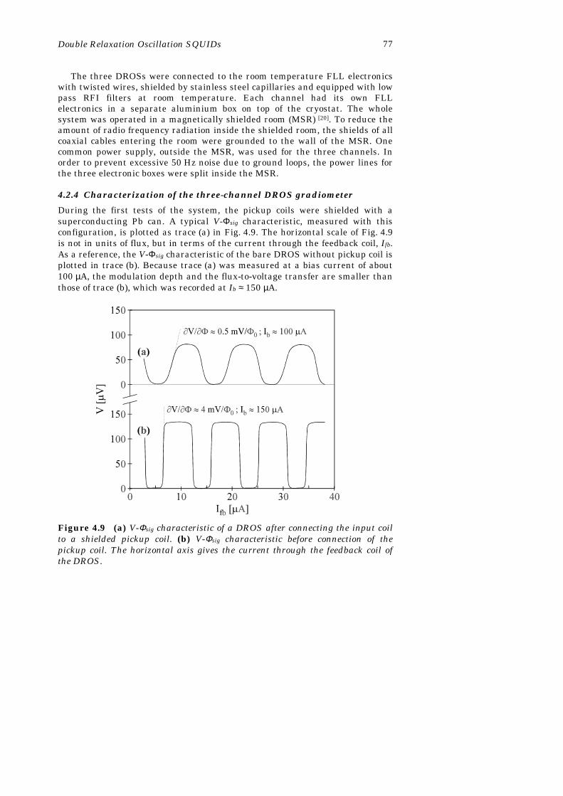
Double Relaxation Oscillation SQUIDs 77
The three DROSs were connected to the room temperature FLL electronicswith twisted wires, shielded by stainless steel capillaries and equipped with lowpass RFI filters at room temperature. Each channel had its own FLLelectronics in a separate aluminium box on top of the cryostat. The wholesystem was operated in a magnetically shielded room (MSR) [20]. To reduce theamount of radio frequency radiation inside the shielded room, the shields of allcoaxial cables entering the room were grounded to the wall of the MSR. Onecommon power supply, outside the MSR, was used for the three channels. Inorder to prevent excessive 50 Hz noise due to ground loops, the power lines forthe three electronic boxes were split inside the MSR.
4.2.4 Characterization of the three-channel DROS gradiometer
During the first tests of the system, the pickup coils were shielded with asuperconducting Pb can. A typical V-Φsig characteristic, measured with thisconfiguration, is plotted as trace (a) in Fig. 4.9. The horizontal scale of Fig. 4.9is not in units of flux, but in terms of the current through the feedback coil, Ifb.As a reference, the V-Φsig characteristic of the bare DROS without pickup coil isplotted in trace (b). Because trace (a) was measured at a bias current of about100 µA, the modulation depth and the flux-to-voltage transfer are smaller thanthose of trace (b), which was recorded at Ib ≈ 150 µA.
Figure 4.9 (a) V-Φsig characteristic of a DROS after connecting the input coilto a shielded pickup coil. (b) V-Φsig characteristic before connection of thepickup coil. The horizontal axis gives the current through the feedback coil ofthe DROS.

Chapter 478
From the periodicity of the V-Φsig characteristics, it can be deduced that Mfb,the mutual inductance between the feedback coil and the signal SQUID,decreased from Mfb = 220 pH to Mfb = 183 pH when the pickup coil wasconnected. This is due to the reduction of the effective signal SQUIDinductance which is screened by the closed superconducting input circuitry. Theoccurrence of this screening effect at low frequencies demonstrates that allcontacts in the flux transformer circuit are superconducting.
Figure 4.10 shows the flux noise spectrum of one of the channels, still withshielded pickup coils. For reference, the flux noise of the same DROS, butwithout pickup coil, is also plotted. Notwithstanding the superconductiveshielding, the white flux noise of the system was degraded by a factor of twoafter the connection of the pickup coils, and amounted to √SΦ = 10 µΦ0/√Hz. Inspite of all precautions, this degradation is probably caused by RFI, picked upby the unshielded twisted wires between the pickup coils and the input coils ofthe DROSs.
After removing the Pb shielding around the pickup coils, the white fluxnoise increased to more than 30 µΦ0/√Hz. In section 4.3.3, it will bedemonstrated that this additional noise is probably due to Johnson noise in theradiation shields of the cryostat. This is confirmed by the observation that theflux noise decreased significantly when the pickup coils were lifted a fewcentimeters above the bottom of the cryostat.
Figure 4.10 Noise spectra of a DROS in the three-channel system before andafter connecting the input coil to a shielded pickup coil. The left vertical axisgives the flux noise, whereas the right axis represents the magnetic field noise.The spike at ∼30 Hz in the upper trace is due to a mechanical vibration.

Double Relaxation Oscillation SQUIDs 79
By measuring the response to the magnetic field of a small coil which waspositioned at various distances below the gradiometric pickup coils and whichcarried an ac current, the field-to-flux transfer of the flux transformers wasdetermined to be ∂B/∂Φsig = 0.4 nT/Φ0 (Aeff = 5.2 mm2). According to Eq. (4.7),this experimental field-to-flux transfer implies that (Lin + Lpu + Lpar) = 0.5 µH.By substituting the design values of Lin = 0.1 µH and Lpu = 0.35 µH, a realisticinductance of Lpar ≈ 50 nH for the 15-cm-long twisted leads between the pickupcoils and the DROSs is deduced.
The right vertical axis of Fig. 4.10 gives the noise in terms of the magneticfield sensitivity, using the experimentally determined value of ∂B/∂Φsig. As canbe seen, the white magnetic field noise of the shielded gradiometer system is√SB = 4 fT/√Hz (10 fT/√Hz @ 1 Hz), which corresponds to a gradiometer noise of1 fT/cm/√Hz (2.5 fT/cm/√Hz @ 1 Hz).
As a direct consequence of the small spacing of less than 1 mm between thethree pickup coils, we clearly observed a low frequency crosstalk when thegradiometer channels were operated simultaneously. If the feedback flux of onechannel was changed by 1 Φ0, the other two channels detected a flux change of5⋅10-3 Φ0. This crosstalk of 5‰ could possibly degrade the sensitivity of theDROSs as the relaxation oscillations in one DROS induce a high frequencyripple on the signal flux of another DROS. Even with Rin-Cin shunts across theinput coils of the DROSs, the amplitude of this ripple can be hundreds of µΦ0.
Fortunately, we did not observe any degradation of the sensitivity when thechannels were operated simultaneously. This could possibly be attributed to thefact that the spectral impurity of the relaxation frequencies of the DROSsspreads the crosstalk signals over such a large bandwidth that the additionalnoise completely drowns in the “normal” flux noise of the DROSs.
4.2.5 Summary
In this section, a three-channel DROS system with wire-wound first-order axialgradiometers was discussed. Typically, the bare DROSs had a white flux noiseof 4.5 µΦ0/√Hz when operated in FLL. This corresponds to an energy sensitivityof ε = SΦ/2Lsq,sig ≈ 275 h. Owing to the large typical flux-to-voltage transfer of0.5 to 1 mV/Φ0, simple room temperature FLL electronics, based on directreadout of the output voltage of the DROSs, could be used without degradingthe sensitivity. When the input coils of the DROSs were connected to the wire-wound pickup coils, the white flux noise rose to about 10 µΦ0/√Hz, despite asuperconducting Pb shield around the pickup coils. This increase may be due toRFI. Nevertheless, the magnetic field sensitivity of √SB = 4 fT/√Hz is amplysufficient for a variety of bio-magnetic measurements. The sensitivity of thesystem decreased when the superconducting shield around the pickup coils wasremoved, which is caused by the Johnson noise in the radiation shields of thecryostat.

Chapter 480
The most important result, however, is that crosstalk at the relaxationfrequency did not decrease the sensitivity of the DROSs, which proves thefeasibility of multi-channel DROS magnetometer systems.
4.3 A planar first-order DROS gradiometer
Using the experience acquired with the development of the three-channelDROS gradiometer, DROSs with a new layout were designed. The mainimprovements with respect to the DROSs of the three-channel system were thegradiometric layout of the signal SQUID, which minimizes the response tohomogeneous magnetic fields and thus relaxes the shielding requirements, andthe implementation of a reference junction instead of a reference SQUID. Insuch a configuration, a single junction with an appropriate critical currentreplaces the reference SQUID. In this way, the number of wires from roomtemperature to the DROS is decreased by two, since the application of thereference flux is not required anymore. A possible disadvantage of a DROSwith a reference junction could be that Ic,ref can no longer be tuned for noiseoptimization. Fortunately, the experimental results in this section show thatthis does not lead to a serious reduction of the sensitivity.
4.3.1 Layout of the gradiometric DROSs
DROSs with a reference junction as well as with a reference SQUID werefabricated in order to be able to compare their respective performance. In theremainder of this chapter, the DROSs with a reference junction will be referredto as “RJ DROSs”, whereas the devices with a reference SQUID will be named“RS DROSs”. Figure 4.11 shows a micrograph and the equivalent scheme of agradiometric RS DROS. The Nb/Al,AlOx/Al/Nb Josephson junctions weredefined by reactive ion etching in an SF6 plasma, whereas all other structures- i.e. the 300 nm thick rf sputtered SiO2 insulating layer, the Pd resistors andthe Nb wiring - were patterned with the lift-off technique.
The signal SQUID consists of two washer-shaped inductors, arranged in agradiometric “figure-8” configuration. As the washers are connected in serieswith the Josephson junctions, homogeneous magnetic fields do not induce largescreening currents in the washers, which would be the case if both washerswere connected in parallel to the junctions [21]. The size of the hole in bothwashers is 50 µm, which corresponds to a total inductance of ∼160 pH. Fromthe measured critical current modulation depth, the actual SQUID inductanceappeared to be significantly larger: Lsq,sig = 550 pH. The additional inductanceis due to the inductance of the double 5-µm-wide and 375-µm-long slit in eachwasher, to the inductance of the connections between the washers and theJosephson junctions, and to the mutual inductance between the two washers.The 2 x 4 µm2 Josephson junctions of the signal SQUID each have a criticalcurrent of 2 to 2.5 µA, implying that βL,sig ≈ 1.2. The estimated junctioncapacitance is 0.25 pF.

Double Relaxation Oscillation SQUIDs 81
The series-connected 25-turns input coils on top of the washers have a totalinductance of Lin ≈ 150 nH and their coupling with the signal SQUID wasmeasured to be Min = 6.7 nH, which implies a coupling coefficient of k = 0.74.The measured mutual inductance between Lsq,sig and the single-turn feedbackcoil, on top of the right SQUID washer in Fig. 4.11, is Mfb = 220 pH.
To minimize the coupling to stray fields, the washer-type reference SQUIDis enclosed by a superconducting shielding loop. The hole size of the referenceSQUID is 50 µm, which, according to Eq. (2.19), corresponds to Lsq,ref ≈ 80 pH.The resulting βL,ref of about 0.2 ensures a large modulation range for Ic,ref. Asingle-turn input coil on top of the reference SQUID is implemented to applythe reference flux. In the RJ devices, the reference SQUID is replaced by asingle 2 x 6 µm2 junction. The critical current of this junction, 3 to 3.5 µA, is inthe middle of the modulation range of Ic,sig(Φsig).
The square shunt inductor, which has a line width of 10 µm and a sidelength of 530 µm, has a designed inductance of Lsh = 1.8 nH [22]. Thegradiometric layout of the signal SQUID minimizes the parasitic magneticcoupling between the shunt inductor and the signal SQUID. The shunt resistorRsh has a resistance of 2 Ω, which yields an effective McCumber parameter ofβC* = 0.027. According to Eq. (4.1), this value of βC* implies a theoreticalmaximum bias current of Ib,max = 27 µA. As the time constant Lsh/Rsh is about1 ns, the relaxation frequency is of the order of 1 GHz. At fRO = 1 GHz,Eq. (4.4b) gives a theoretical white flux noise of √SΦ,theory = 2.9 µΦ0/√Hz.
Figure 4.11 (a) Micrograph and (b) scheme of a gradiometric DROS with areference SQUID. The on-chip resistive input coil shunt can be connected withthe six small bonding pads at the bottom of figure (a). The actual chip size,including the bonding pads, is 2 x 3.3 mm2.

Chapter 482
To avoid Lsh-Csq resonances, every single junction is shunted with a resistorof 40 Ω. Since these shunt resistors do not decrease the βC parameter of thejunctions below unity (βC ≈ 3), the junction hysteresis is not eliminated. Theresulting Rd of 20 Ω implies a damping parameter of D = 2.3, which indicatessufficient damping of the Lsh-Csq resonances. Like in the DROSs of the three-channel system, the signal SQUID inductance is shunted with a resistorRw = 6 Ω to damp L-C resonances between the SQUID inductance and thecapacitances of the Josephson junctions.
Motivated by the positive effect of external Rin-Cin shunts across the inputcoils in the three-channel system, an optional on-chip resistive input coil shuntwas implemented. By means of aluminium bonding wires, the resistance Rin ofthis shunt could be varied between 7.5 Ω and 60 Ω in steps of 7.5 Ω. Thecapacitor Cin was not integrated because of its large area and the associatedhigh probability of shorts through the insulating SiO2 layer.
Unlike the DROSs which have been discussed until now, the output voltageof the gradiometric DROSs was not measured across the reference SQUID orjunction, but across the signal SQUID. As will be explained below, this leads toa slightly larger output voltage swing. The time-averaged voltage <V> acrossthe reference SQUID or junction is either zero (if Ic,sig(Φsig) < Ic,ref) or Vc (ifIc,sig(Φsig) > Ic,ref). This is indicated schematically by the dashed V-Φsig curve inFig. 4.12. The time-averaged voltage across the signal SQUID is either zero (ifIc,sig(Φsig) > Ic,ref) or it modulates with Φsig (if Ic,sig(Φsig) < Ic,ref), since Ic,sig varieswith Φsig. The resulting V-Φsig characteristic is sketched with a solid line in thelower graph of Fig. 4.12. The additional ROS-like modulation which is
Signal SQUID Reference SQUIDjunction size 4 x 2 µm2 junction size 4 x 2 µm2
2I0 4 .. 5 µA b) 2I0 4 .. 5 µA b)
Csq 0.5 pF a) βL,ref ∼0.2 a)
hole size 2 x 50 µm
Lsq,sig ∼550 pH b) Reference junctionβL,sig ∼1.2 b) junction size 6 x 2 µm2
Rw 6 Ω a) I0 3 .. 3.5 µA a)
Input coil Relaxation circuit# turns 2 x 25 Lsh 1.8 a) / 2.1 b) nHline width 4 µm Rsh 2 Ω a,b)
Lin 150 nH b) βC* 0.027 a)
Min 6.7 nH b) Rd 20 Ω a)
k 0.74 D 2.3 a)
a) Design / calculated value.b) Experimental value.
Table 4.2 Main parameters of the gradiometric DROSs.

Double Relaxation Oscillation SQUIDs 83
superposed on the DROS V-Φsig characteristic increases the voltage modulationdepth by a few microvolts.
The main parameters of the gradiometric DROSs are summarized inTable 4.2.
4.3.2 Experimental characteristics of the gradiometric DROSs
The DROSs were characterized using the setup of Fig. 4.5. In the preliminaryexperiments, the effect of external Rin-Cin shunts across the input coils wasinvestigated. The value of Cin was fixed to 1 nF while Rin was varied. The bestresults were obtained for Rin ≤ 50 Ω. In this case, both the flux-to-voltagetransfer and the white flux noise improved by a factor of 2, compared to thesituation without Rin-Cin shunt.
The on-chip input coil shunt resistors were not as effective as the externalshunt circuits. Due to the lack of the dc blocking capacitor Cin, the lowfrequency Johnson noise generated by the integrated resistors directly flowsthrough the input coil, generating a flux noise as high asMin⋅√(4kBT/Rin) = 7 µΦ0/√Hz for Rin = 50 Ω. Therefore, we used external SMDinput coil shunts with Rin = 50 Ω and Cin = 1 nF in all succeeding experiments,unless otherwise specified.
Figures 4.13a and 4.13b show V-Φsig characteristics of an RS DROSrespectively of an RJ DROS. In both graphs, the signal flux was applied via thefeedback coils, and the input coils were shunted with external Rin-Cin circuits.
Figure 4.12 Schematic Ic-Φsig curves (upper graph) and the correspondingV-Φsig characteristics (lower graph) of a DROS, if the output voltage ismeasured across the signal SQUID (solid line, marked “sig”) respectively acrossthe reference SQUID (dashed line, marked “ref”). The dotted line marked“VROS(Φsig)” indicates the V-Φsig characteristic of a ROS.
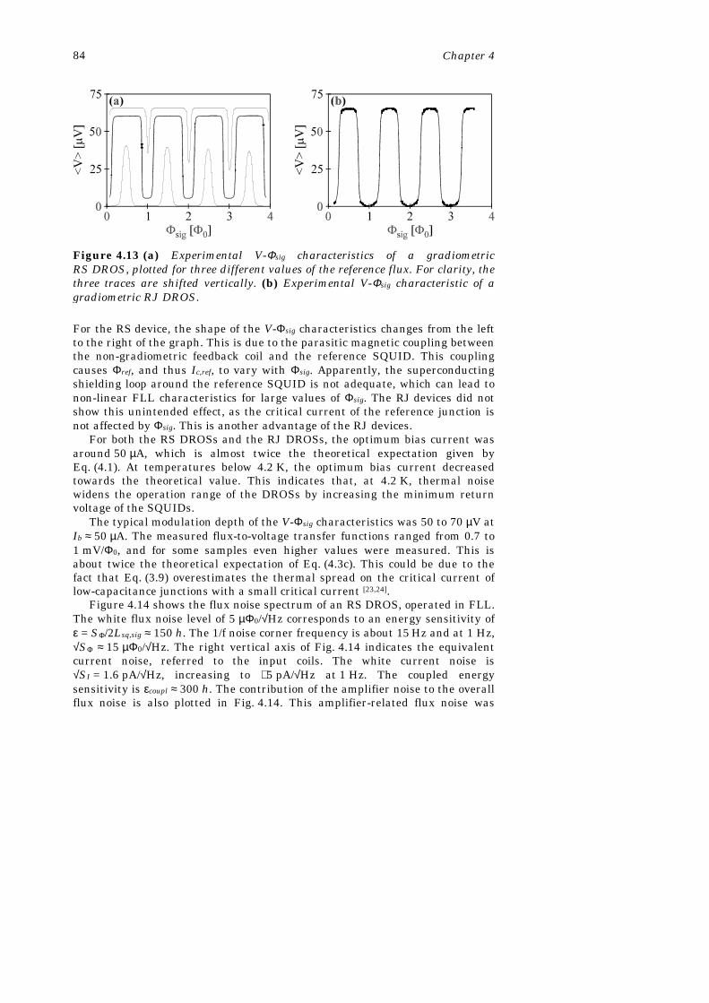
Chapter 484
For the RS device, the shape of the V-Φsig characteristics changes from the leftto the right of the graph. This is due to the parasitic magnetic coupling betweenthe non-gradiometric feedback coil and the reference SQUID. This couplingcauses Φref, and thus Ic,ref, to vary with Φsig. Apparently, the superconductingshielding loop around the reference SQUID is not adequate, which can lead tonon-linear FLL characteristics for large values of Φsig. The RJ devices did notshow this unintended effect, as the critical current of the reference junction isnot affected by Φsig. This is another advantage of the RJ devices.
For both the RS DROSs and the RJ DROSs, the optimum bias current wasaround 50 µA, which is almost twice the theoretical expectation given byEq. (4.1). At temperatures below 4.2 K, the optimum bias current decreasedtowards the theoretical value. This indicates that, at 4.2 K, thermal noisewidens the operation range of the DROSs by increasing the minimum returnvoltage of the SQUIDs.
The typical modulation depth of the V-Φsig characteristics was 50 to 70 µV atIb ≈ 50 µA. The measured flux-to-voltage transfer functions ranged from 0.7 to1 mV/Φ0, and for some samples even higher values were measured. This isabout twice the theoretical expectation of Eq. (4.3c). This could be due to thefact that Eq. (3.9) overestimates the thermal spread on the critical current oflow-capacitance junctions with a small critical current [23,24].
Figure 4.14 shows the flux noise spectrum of an RS DROS, operated in FLL.The white flux noise level of 5 µΦ0/√Hz corresponds to an energy sensitivity ofε = SΦ/2Lsq,sig ≈ 150 h. The 1/f noise corner frequency is about 15 Hz and at 1 Hz,√SΦ ≈ 15 µΦ0/√Hz. The right vertical axis of Fig. 4.14 indicates the equivalentcurrent noise, referred to the input coils. The white current noise is√SI = 1.6 pA/√Hz, increasing to ∼5 pA/√Hz at 1 Hz. The coupled energysensitivity is εcoupl ≈ 300 h. The contribution of the amplifier noise to the overallflux noise is also plotted in Fig. 4.14. This amplifier-related flux noise was
Figure 4.13 (a) Experimental V-Φsig characteristics of a gradiometricRS DROS, plotted for three different values of the reference flux. For clarity, thethree traces are shifted vertically. (b) Experimental V-Φsig characteristic of agradiometric RJ DROS.
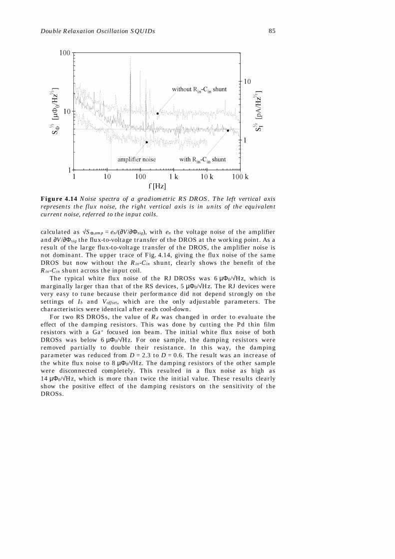
Double Relaxation Oscillation SQUIDs 85
calculated as √SΦ,amp = en/(∂V/∂Φsig), with en the voltage noise of the amplifierand ∂V/∂Φsig the flux-to-voltage transfer of the DROS at the working point. As aresult of the large flux-to-voltage transfer of the DROS, the amplifier noise isnot dominant. The upper trace of Fig. 4.14, giving the flux noise of the sameDROS but now without the Rin-Cin shunt, clearly shows the benefit of theRin-Cin shunt across the input coil.
The typical white flux noise of the RJ DROSs was 6 µΦ0/√Hz, which ismarginally larger than that of the RS devices, 5 µΦ0/√Hz. The RJ devices werevery easy to tune because their performance did not depend strongly on thesettings of Ib and Voffset, which are the only adjustable parameters. Thecharacteristics were identical after each cool-down.
For two RS DROSs, the value of Rd was changed in order to evaluate theeffect of the damping resistors. This was done by cutting the Pd thin filmresistors with a Ga+ focused ion beam. The initial white flux noise of bothDROSs was below 6 µΦ0/√Hz. For one sample, the damping resistors wereremoved partially to double their resistance. In this way, the dampingparameter was reduced from D = 2.3 to D = 0.6. The result was an increase ofthe white flux noise to 8 µΦ0/√Hz. The damping resistors of the other samplewere disconnected completely. This resulted in a flux noise as high as14 µΦ0/√Hz, which is more than twice the initial value. These results clearlyshow the positive effect of the damping resistors on the sensitivity of theDROSs.
Figure 4.14 Noise spectra of a gradiometric RS DROS. The left vertical axisrepresents the flux noise, the right vertical axis is in units of the equivalentcurrent noise, referred to the input coils.

Chapter 486
For an experimental determination of the value of Lsh, the relaxationfrequency of a gradiometric ROS was measured. The layout of this ROS wasidentical to that of the DROSs, except of course for the lack of a referenceSQUID or junction. Initially, we intended to measure the relaxation frequencyas a function of the applied flux, using the setup and the procedure which wasdescribed in chapter 3. However, due to the low critical current of the junctions,the high frequency output power was below the detection limit of the setup.Therefore, gradiometric ROSs with a much larger critical current, 2I0 = 105 µA,were fabricated in a new production run. Figure 4.15a shows the outputspectrum of such a ROS, oscillating at fRO = 625 MHz. Besides the peak at thefundamental frequency, also the harmonics at ∼1.3 GHz and at ∼1.9 GHz arevisible. Due to the large value of βL,sig ≈ 30, the relaxation frequency showed avery small modulation with Φsig. Therefore, Lsh was determined from fRO-Ib
measurements instead of fRO-Φsig measurements.The markers in Fig. 4.15b show the measured fRO-Ib relation. The solid line
is a fit, calculated via the method of section 3.3.4, using Lsh = 2.1 nH andTV = 225 ps. The agreement between the fit value and the design value of Lsh isnoticeable, especially if one considers that the experimental value of Lsh alsocomprises “parasitic” inductances, such as the SQUID inductance.
Figure 4.15 (a) Spectrum of the high frequency output signal of a gradiometricROS with 2I0 = 105 µA at a bias current of 163 µA. The frequency of therelaxation oscillations is 625 MHz. The vertical scale has not been corrected forthe gain of the pre-amplifier, which is about 25 dB. (b) Experimental fRO vs. Ib
characteristic (markers) with theoretical fit (solid line). The fit value for Lsh is2.1 nH.

Double Relaxation Oscillation SQUIDs 87
4.3.3 Gradiometric DROSs with external planar gradiometers
Using gradiometric RJ DROSs, two gradiometer systems with external planarpickup coils were realized. A photograph of one of the assembled gradiometersis shown in Fig. 4.16. The DROSs were glued to an epoxy printed circuit board(PCB) which also contained the SMD Rin-Cin input coil shunt. The PCB wasfixed to the glass substrate of the pickup coils with TRZ 0004 epoxy [25]. Theconnections between the input coils and the pickup circuit were made with50-µm-thick and 1-cm-long Nb bonding wires [19].
Figure 4.16 Photograph of the assembled 2 x 2 cm2 planar gradiometer.
2 x 2 cm2 1 x 1 cm2
d 20 10 mm
w 1.2 0.56 mm
s 0.05 0.04 mm
b 40 40 mm
Lpu 100 a) 60 a) nH
Apu 352 a) 89 a) mm2
∂B/∂Φsig 0.23 b) 0.78 b) nT/Φ0
Aeff 9.0 b) 2.7 b) mm2
a) Design / calculated value.b) Experimental value.
Table 4.3 Parameters of the planar gradiometric pickup coils that wereconnected to the gradiometric RJ DROSs.

Chapter 488
The planar first-order pickup coils consisted of a 500 nm thick dc magnetronsputtered Nb film on a glass substrate of 75 mm x 25 mm x 1 mm. Twogradiometers were constructed: one with d = 2 cm and one with d = 1 cm, withd as defined in Fig. 4.16. Both gradiometers had a baseline of b = 4 cm. The linewidth w of the pickup coils was calculated to maximize the effective area Aeff ofthe gradiometers. The parameters of the pickup coils are listed in Table 4.3.
The effective areas which are listed in Table 4.3 were determined bymeasuring the response of the gradiometers to the magnetic field of a long(∼2 m) straight wire, carrying an alternating current. From the experimentallydetermined values of Aeff, the inductances in the flux transformer circuits couldbe calculated via Eq. (4.7). For the 2 x 2 cm2 gradiometer, this resulted inLin + Lpar = 162 nH, and the 1 x 1 cm2 gradiometer yielded the almost identicalvalue of Lin + Lpar = 164 nH. Estimating the parasitic inductance of the1-cm-long Nb bonding wires to Lpar = 10 .. 15 nH [26], these results imply aninput coil inductance of Lin ≈ 150 nH, which value has been printed inTable 4.2.
The first noise measurements were carried out inside a superconducting Nbshielding. Figure 4.17 shows the noise characteristics of the gradiometer with2 x 2 cm2 pickup coils. The sensitivity of the DROS was not degraded by the
Figure 4.17 Noise spectra of a gradiometric DROS with reference junction,coupled to an external 2 x 2 cm2 planar gradiometer. The left vertical axis is inunits of the flux noise, and the right vertical axis gives the equivalent magneticfield noise. The inset shows a part of the traces (a), (b) and (c) on an enlargedvertical scale.

Double Relaxation Oscillation SQUIDs 89
connection of the gradiometer, the white flux noise level even decreased from6 µΦ0/√Hz [ trace (b) ] to 5 µΦ0/√Hz [ trace (a) ]. This is due to screening of Lsq,sig
by the superconducting flux transformer. The low frequency part of trace (a) isnot shown since it was quite irregular due to mechanical vibrations andmicrophonics. The white flux noise of 5 µΦ0/√Hz corresponds to a magnetic fieldresolution of √SB = 1.2 fT/√Hz or, equivalently, a gradiometer noise of0.3 fT/cm/√Hz.
After these preliminary measurements, the gradiometers were mounted in anon-magnetic fiberglass probe, and cooled down in the same BTI BMD-5 dewarwhich was used for the three-channel system. The noise spectrum of thisconfiguration, measured in a magnetically shielded room [20], is plotted intrace (d) of Fig. 4.17. The noise increased drastically to √SΦ = 65 µΦ0/√Hz(√SB = 15 fT/√Hz). In this cryostat, the sensitivity of the three-channel systemalso degraded, and therefore the cryostat was suspected to be at the origin ofthe additional noise. To verify this hypothesis, we adapted the non-magneticinsert for use in a modern CTF SST-140 non-magnetic dewar. As trace (c) ofFig. 4.17 shows, the white flux noise in this “new” cryostat was significantlylower, 7 to 8 µΦ0/√Hz, corresponding to a magnetic field noise better than2 fT/√Hz. This clearly indicates that the BMD-5 cryostat was the source of theexcess noise.
At lower frequencies, trace (c) in Fig. 4.17 is somewhat irregular, which isprobably due to residual noise in the MSR and to mechanical vibrations.Nevertheless, the magnetic field resolution at 1 Hz is still ∼10 fT/√Hz. Todemonstrate the operation of the system, some simple bio-magneticmeasurements were carried out. An example of such a measurement is themagnetic heart signal which was shown in Fig. 1.1.
The gradiometer with 1 x 1 cm2 pickup coils has also been characterized. Asa direct result of its smaller effective area (Aeff = 2.7 mm2 instead of 9 mm2), thewhite magnetic field noise was larger than for the gradiometer with the2 x 2 cm2 pickup coils. Nevertheless, its white magnetic field resolution of about4.5 fT/√Hz is sufficient for bio-magnetic measurements.
4.3.4 Summary
In this section, the development of planar first-order gradiometers based onDROSs was described. To minimize the direct pickup of magnetic fields, theDROSs had a gradiometric signal SQUID. The white flux noise of the bareDROSs was about 5 µΦ0/√Hz when operated in FLL, corresponding to anenergy sensitivity of ε ≈ 150 h. Owing to the large flux-to-voltage transfer of thedevices, 0.7 to 1 mV/Φ0 typically, the amplifier noise did not dominate theoverall flux noise. The coupled energy sensitivity of the devices wasεcoupl ≈ 300 h.
Besides DROSs with a reference SQUID, also DROSs with a referencejunction were developed and characterized. The flux noise level of thesedevices, ∼6 µΦ0/√Hz, was only slightly larger than that of the devices with a

Chapter 490
reference SQUID. The devices with a reference junction were very user-friendlyand easy to tune, and required two wires less for operation.
The characteristics of the DROSs did not degrade when the input coils wereconnected to external flux transformers. Coupled to an external planargradiometric pickup coil with a coil size of 2 x 2 cm2 and a baseline of 4 cm, thewhite magnetic field noise inside a superconducting shielding was only1.2 fT/√Hz (7 fT/√Hz @ 1 Hz). Inside a magnetically shielded room, withoutadditional shields around the gradiometer, the white field noise was still below2 fT/√Hz (∼10 fT/√Hz @ 1 Hz). This magnetic field resolution matches that ofother state-of-the-art SQUID systems.
4.4 A directly coupled multi-loop DROS magnetometer
In sections 4.2 and 4.3, external pickup circuits were connected to the DROSsto increase the effective sensing area and thus the response to magnetic fields.Although such configurations work fine, they give rise to complications inmulti-channel SQUID systems, for example because of the limited reliability ofthe superconducting contacts between the pickup coils and the input coils.Moreover, a system composed of many separate components is not well suitedfor mass production. A possible solution to overcome these limitations is theintegration of the entire flux transformer on the same substrate as the DROS,as was demonstrated by Lee et al. [27]. Another configuration, the directlycoupled multi-loop DROS magnetometer, is discussed in this section.
In a directly coupled SQUID, the magnetic field is sensed directly by theSQUID inductance, without intermediate flux transformer. Therefore, thegeometry of the SQUID should combine two seemingly contradictoryproperties: a large effective area for optimum field-to-flux transfer and a smallinductance in order to keep the βL parameter reasonably small. By connectingseveral large loops in parallel, these two requirements can be combined. Multi-loop dc SQUIDs with APF circuits have been applied in several multi-channelbio-magnetometer systems [28,29], and in this section it will be shown that themulti-loop structure is also applicable for DROSs.
4.4.1 Layout of the multi-loop DROS magnetometer
A photograph and the scheme of the multi-loop DROS are printed in Fig. 4.18.The eight loops, arranged like the parts in a round pie, are connected inparallel in the central area of the device. The entire structure has a diameter of8 mm. According to the theory of Drung et al. [22], the inductance of the multi-loop signal SQUID amounts to Lsq,sig = 410 pH and its theoretical effective areais Aeff = 4.9 mm2.
The damping resistors, the washer-type reference SQUID and theJosephson junctions of the signal SQUID are located in the center of the device.Two superconducting shielding loops prevent direct pickup of the magneticfield by the reference SQUID. The 4 x 4 µm2 Nb/Al,AlOx/Al/Nb Josephson

Double Relaxation Oscillation SQUIDs 91
junctions have a critical current of 7 µA each, and their presumed capacitanceis Cj = 0.5 pF. The βL parameter of the signal SQUID is βL,sig ≈ 2.8.
The shunt resistor Rsh has a value of 2 Ω and is positioned at the lower leftcorner of Fig. 4.18. According to Eq. (4.1), the resulting value of βC* = 0.17implies a theoretical maximum bias current of 34 µA. By connecting the biascurrent in the middle of one pickup loop, at the lower left of Fig. 4.18, aninductance of ∼¼⋅Lloop ≈ 0.8 nH is introduced in the relaxation circuit.Therefore, no additional discrete shunt inductor Lsh is required. The timeconstant of the relaxation circuit, Lsh/Rsh ≈ 0.5 ns, suggests a relaxationfrequency of a few GHz.
Each junction is shunted by a resistor 2Rd = 20 Ω to damp the Lsh-Csq
resonances. The damping parameter of D ≈ 2 indicates sufficient damping. Inorder to prevent Lsq-Cj resonances in the signal SQUID, the SQUID inductanceis shunted at two sites with additional damping resistors of 2Rw = 20 Ω.
The feedback flux is applied by means of the small feedback coil in the upperleft corner of the photograph. The main parameters of the multi-loop DROS aresummarized in Table 4.4.
4.4.2 Experimental characteristics of the multi-loop DROS
The devices showed optimum performance at bias currents around 30 µA,which is in good agreement with the theoretical maximum bias current of34 µA. Trace (a) in Fig. 4.19 shows a V-Φsig characteristic of a multi-loop DROS,measured in a superconducting Nb/Pb shielding. The typical voltage
Figure 4.18 (a) Micrograph and (b) scheme of the directly coupled multi-loopDROS magnetometer. The diameter of the entire structure is 8 mm. The dashedlines indicate the positions were the central connections of the damping resistorswere cut with a Ga+ focused ion beam. For clarity, the coil for applying thereference flux and the associated bonding pads are not indicated in figure (b).

Chapter 492
modulation depth of the devices was between 40 and 50 µV, which is inaccordance with the theoretical expectation of Eq. (4.2). However, theexperimental flux-to-voltage transfer of about 180 µV/Φ0 is below thetheoretical expectation of ∼300 µV/Φ0 almost by a factor of two.
When the temperature of the helium bath was decreased to about 2 K, theslopes of the V-Φsig characteristic became steeper, as shown in trace (b) ofFig. 4.19. This indicates that the reduction of the flux-to-voltage transfer is notdue to external sources, e.g. RFI, but that it is caused by thermal effects in theDROS itself. The asymmetry in the V-Φsig curves at 2 K may be caused by asmall “APF-effect” due to parasitic magnetic coupling between the differentelements of the DROS.
To investigate whether the Johnson noise generated by the resistors 2Rw
could be at the origin of the small value of ∂V/∂Φsig, we cut these two resistorswith a Ga+ focused ion beam (FIB). However, this had no effect on the slope ofthe V-Φsig curves. In a second attempt to find the cause of the reduced flux-to-voltage transfer, we changed the configuration of the damping resistors 2Rd.The central connections were cut with the FIB at the positions indicated withdashed lines in Fig. 4.18b. As trace (c) in Fig. 4.19 shows, ∂V/∂Φsig increased byabout 50% as a result of this action. This clearly shows that the dampingresistors 2Rd affect the flux-to-voltage transfer of the multi-loop DROSmagnetometer.
A simple way to evaluate the effect of the Johnson noise generated by thedamping resistors is to assume that it increases the spread on the criticalcurrents of the reference SQUID and the signal SQUID. According to Eq. (3.9),at T = 4.2 K, the thermally induced critical current spread of both dc SQUIDs
Multi-loop signal SQUID Washer-type reference SQUIDdiameter 8 mm junction size 4 x 4 µm2
junction size 4 x 4 µm2 2I0 16 µA b)
2I0 14 µA b) hole size 20 µm
Csq 1 pF a) Lsq,ref 35 pH b)
Lsq,sig 410 pH a) βL,ref ∼0.25 b)
βL,sig 2.8 a)
Aeff 4.9 a) / 4.1 b) mm2 Relaxation circuitRw 10 Ω a) Lsh ∼0.8 nH a)
Rsh 2 Ω b)
βC* 0.17 a)
Rd 10 Ω a)
D 2 a)
a) Design / calculated value.b) Experimental value.
Table 4.4 Main parameters of the multi-loop directly coupled DROSmagnetometers.

Double Relaxation Oscillation SQUIDs 93
amounts to ∆Ic,thermal = 0.60 µA. In the original configuration, each junction isshunted by a resistor of 2Rd = 20 Ω, generating a Johnson noise of√SI = 3.4 pA/√Hz. The effective bandwidth of this Johnson noise can beapproximated with the plasma frequency of the junctions, fp = 33 GHz. Thisleads to a root mean square (rms) value of ∆Ic,Johnson = 0.62 µA for the criticalcurrent spread caused by the Johnson noise. Because the Johnson noise andthe thermal critical current noise are not correlated, they should be addedquadratically, resulting in ∆Ic,total = √(0.622 + 0.602) = 0.86 µA. With this valuefor the total spread on the critical currents of the SQUIDs, Eqs. (4.3b)and (4.3a) yield ∂V/∂Φsig ≈ 210 µV/Φ0 if Vc = 45 µV is substituted. This is inreasonable agreement with the experimentally observed flux-to-voltagetransfer of 180 µV/Φ0.
Figure 4.19 V-Φsig characteristics of a multi-loop DROS recorded at a biascurrent of 30 µA in three different cases: (a) original configuration, T = 4.2 K;(b) original configuration, T ≈ 2 K; (c) central connection of the dampingresistors removed with a Ga+ focused ion beam, T = 4.2 K.

Chapter 494
In the multi-loop DROSs which were modified with the FIB, the value of theresistors was doubled to 40 Ω. The associated Johnson noise is now 2.4 pA/√Hz,causing an additional critical current noise of ∆Ic,Johnson = 0.44 µA. Then, thetotal critical current noise is ∆Ic,total = 0.74 µA per SQUID. Via Eqs. (4.3b)and (4.3a), this leads to ∂V/∂Φsig ≈ 250 µV/Φ0. Again, this is close to theexperimentally observed value of 280 µV/Φ0. Thus, this simple model givesrealistic values for the flux-to-voltage transfer, both before and after changingthe layout of the damping resistors with the FIB.
The effective area of the multi-loop DROSs was measured inside amagnetically shielded room [20] by positioning an ac magnetic dipole at variousdistances below the magnetometers. The result, Aeff = 4.1 mm2 (i.e.∂B/∂Φsig = 0.5 nT/Φ0), is below the theoretical value of 4.9 mm2 which wasobtained with the theory of Drung et al. The origin of this discrepancy is notclear. The experimentally determined value of the effective area could beverified by means of a setup with a Helmholtz coil instead of a magnetic dipole.However, this double-check has not been performed.
Due to the relatively low flux-to-voltage transfer of the multi-loop DROSmagnetometers, their sensitivity was limited by the input voltage noise of theroom temperature electronics, 3.3 nV/√Hz in the white region. This isconsiderably above the amplifier noise (1.8 nV/√Hz) because of the Johnsonnoise generated in the room temperature RFI-filters, which had a resistance of450 Ω. The best white noise in FLL, √SΦ = 14 µΦ0/√Hz (√SB = 7 fT/√Hz), wasobtained for the “FIB-DROSs”, which had the highest flux-to-voltage transfer.The intrinsic noise was in the range √SΦ,intr = 6 .. 8 µΦ0/√Hz (√SB,intr =3 .. 4 fT/√Hz), but the exact value was difficult to determine because of thelarge contribution of the amplifier noise to the total flux noise.
4.4.3 Summary
In this section, an eight-loop directly coupled DROS magnetometer wasdiscussed. The large effective area of this device makes a separate fluxtransformer superfluous, which is a large advantage in multi-channelmagnetometer systems. However, due to the Johnson noise generated by thedamping resistors, the flux-to-voltage transfer of the devices was limited to∂V/∂Φsig = 180 µV/Φ0. With a focused ion beam, the connections of the dampingresistors were rearranged, resulting in a larger transfer coefficient of about280 µV/Φ0. A simple model, giving a quantitative explanation of these results,was presented. The - amplifier limited - magnetic field sensitivity of thedirectly coupled DROSs with the modified layout was √SB = 7 fT/√Hz in thewhite region. A thorough experimental and theoretical study of the effect of theJohnson noise generated in the damping resistors could lead to a furtherimprovement of the DROS characteristics.

Double Relaxation Oscillation SQUIDs 95
4.5 A DROS-based current gauge
Until now, only DROS-based systems for magnetometry have been discussed.Nevertheless, all physical quantities that can be converted to a magnetic flux- e.g. mechanical displacements or electric currents - can be measured withSQUIDs, which widens the field of applications considerably. In this section, aDROS is used as a very sensitive current gauge, which is demonstrated bymeasuring the subgap I-V characteristic of a voltage biased high qualityNb/Al,AlOx/Al/Nb superconducting tunnel junction (STJ).
This type of measurement is for instance of relevance for the readout of X-ray spectrometers based on STJs [30]. The principle of operation of suchspectrometers is based on the fact that the subgap current of a voltage biasedtunnel junction rises momentarily when an X-ray photon is absorbed. Themagnitude of this current rise, typically a few µA, is a measure for the energyof the incident photon. Since the signal only lasts for some microseconds, thecurrent gauge which measures the subgap current should have a bandwidth ofmore than 1 MHz. For sufficient current resolution, its noise should not exceeda few pA/√Hz [31]. A last requirement for the current gauge is a low impedancefor optimum voltage biasing of the STJ.
A standard non-hysteretic dc SQUID with an integrated superconductinginput coil has the required current sensitivity. However, due to the fluxmodulated readout scheme, it is difficult - although not impossible [32,33] - toobtain the required FLL bandwidth of several MHz. Second generation SQUIDslike the dc SQUID array, the APF SQUID or the DROS have a non-modulatedreadout scheme, enabling high bandwidth operation with a relatively simplesystem layout [16,34].
Figure 4.20 shows the scheme of the setup that was used for the I-Vmeasurements with a DROS. A gradiometric DROS with a reference junction,of the type which has been discussed in detail in section 4.3, was used tomeasure the current Istj through the STJ, which was mounted on the sameepoxy printed circuit board as the DROS. The room temperature flux lockedloop electronics, identical to that of Fig. 4.5, is not indicated in Fig. 4.20. TheSTJ was voltage biased with a small SMD resistor Rx, located in the vicinity ofthe junction. We used two values for this resistor, 1.5 Ω and 3.7 Ω. Since Rx ismuch smaller than the dynamic resistance of the STJ, the junction is biased ata voltage V = Ib,x⋅Rx. The bias voltage Vstj was measured with a roomtemperature differential amplifier, not indicated in Fig. 4.20. The DROS andthe STJ were shielded from environmental electromagnetic noise with a Nbshield. All wires from room temperature to the cryogenic environment wereRFI filtered, and in the lines which were connected to the input coil of theDROS, cooled series resistors of a few kΩ were mounted for additional filtering.

Chapter 496
Figure 4.20 Scheme of the setup which was used to measure the current versusvoltage characteristic of a voltage biased superconducting tunnel junction (STJ)with a DROS.
Figure 4.21 Measured subgap I-V characteristics of a voltage biased STJ witha large excess current in the subgap. Solid line: measured with the DROS-basedsetup of Fig. 4.20. Dotted line: measured with standard I-V electronics. Forclarity, the dotted line is shifted vertically by about 0.25 µA. The right verticalaxis is in units of the flux coupled to the DROS.

Double Relaxation Oscillation SQUIDs 97
During the initial tests of the system, a low quality STJ with a large excesscurrent in the subgap was used. The measured I-V characteristic of this STJ isplotted in Fig. 4.21. For comparison, the I-V characteristic which was measuredwith conventional I-V electronics is also plotted in the graph. Thecorrespondence between the two traces is good, which demonstrates that thesetup operates properly.
The STJ could be biased with high stability at voltages down to its minimumreturn voltage [ Eq. (2.8b) ] of a few hundred microvolts. At lower voltages, thebias circuit starts to act as a relaxation oscillator. The frequency of therelaxation oscillations in the bias circuit is determined by the time constantLin/Rx, with Lin the inductance of the input coil of the DROS. In the presentsetup, this time constant is about 100 ns, which implies a relaxation frequencyof approximately 10 MHz.
Experimentally, this relaxation oscillation effect was observed in two ways.First, at a bias voltage between 100 and 200 µV, the Ib,x-Vstj characteristicshowed a discontinuity, marking the transition from the oscillating mode to thestable mode. Second, at bias voltages below ∼150 µV, the V-Φ modulation of theDROS disappeared completely, because the relaxation oscillations generated inthe bias circuit swept the input flux of the DROS over more than 100 Φ0 at afrequency of about 10 MHz, wiping out the V-Φ modulation completely.
After the preliminary tests, the “bad” STJ was replaced by a high quality10 x 10 µm2 STJ. At 4.2 K, the critical current of this STJ was measured to beI0 = 37 µA, and its quality parameter was Vm = 70 mV. Here, Vm is defined asVm = π/4 ⋅ Vg/RN ⋅ 2 mV/I2mV, with Vg = 2.8 mV the gap voltage, RN = 42 Ω thenormal resistance at V » Vg and I2mV = 1.5 µA the subgap current at V = 2 mV.
In Fig. 4.22, measured current versus voltage characteristics of this STJ areplotted for different temperatures of the 4He bath. Because a SQUID operatedin FLL only measures flux changes and not absolute values, the vertical offsetsin Fig. 4.22 are arbitrary, and different for each trace. As the STJ is voltagebiased, also parts of the I-V trace with a negative dynamic resistance can bemeasured. Another advantage of the voltage biasing circuit is the elimination ofthe need for an external magnetic field to suppress the critical current of theSTJ. Therefore, the subgap structure is not obscured by Fiske steps [35].
The peak at V = 260 µV in the 4.2 K trace is caused by the differencebetween the gap energy in the bottom and the top electrode of the STJ. Thesensitivity of the DROS is demonstrated in the inset of Fig. 4.22, which showsan enlargement of a part of the 1.6 K trace. Small structures of less than 1 nAare revealed clearly, and the sharp rise of the subgap current at half the gapvoltage is evident [36]. The measurements of Fig. 4.22 were reproduced inseveral subsequent cool-downs.
The bandwidth of the present flux locked loop setup is about 250 kHz. Afterupgrading the readout electronics to a higher bandwidth, the system will beapplicable in the field of X-ray spectroscopy. DROSs are also good candidatesfor the readout of other types of cryogenic sensors, for instance micro-bolometers with a transition-edge sensor [37].
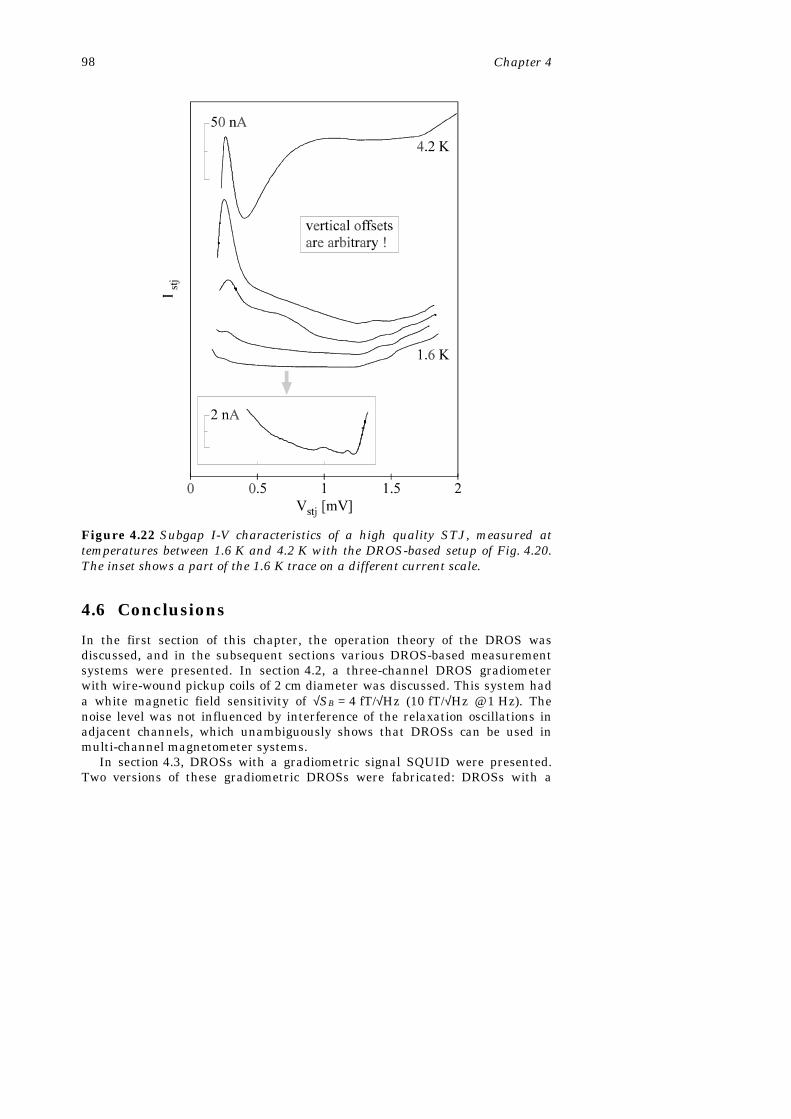
Chapter 498
4.6 Conclusions
In the first section of this chapter, the operation theory of the DROS wasdiscussed, and in the subsequent sections various DROS-based measurementsystems were presented. In section 4.2, a three-channel DROS gradiometerwith wire-wound pickup coils of 2 cm diameter was discussed. This system hada white magnetic field sensitivity of √SB = 4 fT/√Hz (10 fT/√Hz @ 1 Hz). Thenoise level was not influenced by interference of the relaxation oscillations inadjacent channels, which unambiguously shows that DROSs can be used inmulti-channel magnetometer systems.
In section 4.3, DROSs with a gradiometric signal SQUID were presented.Two versions of these gradiometric DROSs were fabricated: DROSs with a
Figure 4.22 Subgap I-V characteristics of a high quality STJ, measured attemperatures between 1.6 K and 4.2 K with the DROS-based setup of Fig. 4.20.The inset shows a part of the 1.6 K trace on a different current scale.

Double Relaxation Oscillation SQUIDs 99
reference SQUID (RS DROSs) and DROSs with a reference junction(RJ DROSs). The white flux noise of the RS DROSs (√SΦ = 5 µΦ0/√Hz, ε ≈ 150 h)was slightly better than that of the RJ devices (√SΦ = 6 µΦ0/√Hz, ε ≈ 200 h), butthe RJ DROSs required less wires from the room temperature electronics to thecryogenic environment, and they were easier to operate. Moreover, the V-Φsig
characteristics of the RJ DROSs were not distorted by parasitic coupling of thesignal flux to the reference SQUID. With an external planar gradiometricpickup coil of 2 x 2 cm2, a magnetic field sensitivity better than 2 fT/√Hz wasmeasured inside a magnetically shielded room.
In section 4.4, a directly coupled multi-loop DROS magnetometer wasdiscussed. Owing to the multi-loop structure, this DROS combined a largeeffective area of 4.1 mm2 with a moderate SQUID inductance of 410 pH.However, due to the Johnson noise generated in the damping resistors, theflux-to-voltage transfer of these devices was limited to ∂V/∂Φsig = 180 µV/Φ0.After reconfiguration of the layout of the damping resistors, using a focused ionbeam, the flux-to-voltage transfer increased to 280 µV/Φ0. A simple model waspresented to explain this increase quantitatively. As a direct result of thelimited flux-to-voltage transfer coefficient, the sensitivity of the multi-loopDROS magnetometer, √SB = 7 fT/√Hz, was limited by the noise of the readoutamplifier at room temperature.
Finally, in section 4.5, a gradiometric RJ DROS was used to measure thecurrent through a voltage biased Nb/Al,AlOx/Al/Nb tunnel junction. The goodcurrent sensitivity of 2 pA/√Hz allowed variations below 1 nA to be observedclearly in the subgap I-V characteristics of the tunnel junction. These resultsdemonstrate that DROSs are promising candidates for the readout of cryogenicsensors.
References1 D.J. Adelerhof, J. Kawai, G. Uehara and H. Kado, “High sensitivity double relaxation
oscillation superconducting quantum interference devices”, Appl. Phys. Lett. 65,2606-2608 (1994).
2 D.J. Adelerhof, J. Kawai, G. Uehara and H. Kado, “High sensitivity double relaxationoscillation superconducting quantum interference devices with large transfer from flux tovoltage”, Rev. Sci. Instrum. 66, 2631-2637 (1995).
3 M.J. van Duuren, Y.H. Lee, D.J. Adelerhof, J. Kawai, H. Kado, J. Flokstra and H. Rogalla,“Multichannel SQUID magnetometry using double relaxation oscillation SQUIDs”, IEEETrans. Appl. Supercond. 6, 38-44 (1996).
4 J. Vrba, “SQUID gradiometers in real environments”, in SQUID Sensors: Fundamentals,Fabrication and Applications, ed. H. Weinstock, NATO ASI Series 329, Kluwer AcademicPublishers, Dordrecht / Boston / London (1996).
5 M.J. van Duuren, G.C.S. Brons, D.J. Adelerhof, J. Flokstra and H. Rogalla, “Doublerelaxation oscillation superconducting quantum interference devices with gradiometriclayout”, J. Appl. Phys. 82, 3598-3606 (1997).

Chapter 4100
6 D.J. Adelerhof, H. Wichers, C. Brons, M. van Duuren, D. Veldhuis, J. Flokstra and H.Rogalla, “Direct coupled multi-loop DROS magnetometer with direct voltage readout”, inproc. International Superconductive Electronics Conference (ISEC), Nagoya, Japan, 371-373(1995).
7 G.H. Chen, H.Y. Zhai and Q.S. Yang, “Flux to voltage transfer function and noise in doublerelaxation oscillation SQUIDs”, IEEE Trans. Appl. Supercond. 7, 3477-3480 (1997).
8 D.J. Adelerhof, M.J. van Duuren, J. Flokstra and H. Rogalla, “High sensitivity magneticflux sensors with direct voltage readout: Double relaxation oscillation SQUIDs”, IEEETrans. Appl. Supercond. 5, 2160-2163 (1995).
9 Superconducting Sensor Laboratory, 2-1200 Muzaigakuendai Inzai, Chiba 270-13, Japan.10 D.J. Adelerhof, J. Kawai, K. Tsukada, G. Uehara and H. Kado, “Magnetometers based on
double relaxation oscillation superconducting quantum interference devices”, Appl. Phys.Lett. 66, 2274-2276 (1995).
11 M.B. Ketchen, “Design considerations for dc SQUIDs fabricated in deep sub-microntechnology”, IEEE Trans. Magn. 27, 2916-2919 (1991).
12 K. Enpuku, K. Sueoka, K. Yoshida and F. Irie, “Effect of damping resistance on voltageversus flux relation of a dc SQUID with large inductance and critical current”, J. Appl.Phys. 57, 1691-1697 (1985).
13 R.H. Koch, V. Foglietti, J.R. Rozen, K.G. Stawiasz, M.B. Ketchen, D.K. Lathrop, J.Z. Sunand W.J. Gallagher, “Effects of radio frequency radiation on the dc SQUID”, Appl. Phys.Lett. 65, 100-102 (1994).
14 The LT 1028 op-amp is manufactured by the Linear Technology Corporation, Milpitas (CA),U.S.A.
15 D. Drung, “Advanced SQUID read-out electronics”, in SQUID Sensors: Fundamentals,Fabrication and Applications, ed. H. Weinstock, NATO ASI Series 329, Kluwer AcademicPublishers, Dordrecht / Boston / London (1996).
16 D. Drung, T. Radic, H. Matz and H. Koch, “A 2-channel wideband SQUID system for high-frequency geophysical applications”, IEEE Trans. Appl. Supercond. 7, 3283-3286 (1997).
17 K. Enpuku, R. Cantor and H. Koch, “Modeling the direct current superconducting quantuminterference device coupled to the multiturn input coil. II.”, J. Appl. Phys. 71, 2338-2346(1992).
18 BTI type BMD 5.19 W. Jaszczuk, H.J.M. ter Brake, J. Flokstra, D. Veldhuis, R. Stammis and H. Rogalla,
“Bonding of a niobium wire to a niobium thin film”, Meas. Sci. Technol. 2, 1121-1122 (1991).20 Vacuumschmelze type AK-3B.21 M.B. Ketchen, “Integrated thin-film dc SQUID sensors”, IEEE Trans. Magn. 23, 1650-1657
(1987).22 D. Drung, S. Knappe and H. Koch, “Theory for the multiloop dc superconducting quantum
interference device magnetometer and experimental verification”, J. Appl. Phys. 77,4088-4098 (1995).
23 D.J. Adelerhof, Second generation dc SQUID magnetometers: (Double) RelaxationOscillation SQUIDs, Ph.D. thesis University of Twente, Enschede (1993).
24 D.J. Adelerhof, H. Nijstad, J. Flokstra and H. Rogalla, “(Double) relaxation oscillationSQUIDs with high flux-to-voltage transfer: Simulations and experiments”, J. Appl. Phys.76, 3875-3886 (1994).
25 TRZ 0004 epoxy is manufactured by Oxford Instruments, Old Station Way, Eynsham,Witney, Oxon OX8 1TL, U.K.
26 F.W. Grover, Inductance calculations, working formulas and tables, Dover Publications Inc.,New York (1962).

Double Relaxation Oscillation SQUIDs 101
27 Y.H. Lee, H.C. Kwon, J.M. Kim, Y.K. Park and J.C. Park, ”An integrated planargradiometer based on a double relaxation oscillation SQUID”, Supercond. Sci. Technol. 9,A34-A37 (1996).
28 D. Drung, “The PTB 83-SQUID system for biomagnetic applications in a clinic”, IEEETrans. Appl. Supercond. 5, 2112-2117 (1995).
29 K. Kazami, Y. Takada, G. Uehara, N. Matsuda and H. Kado, “Evaluation of Drung-typemagnetometers for multi-channel systems”, Supercond. Sci. Technol. 7, 249-252 (1994).
30 N.E. Booth and D.J. Goldie, “Superconducting particle detectors”, Supercond. Sci. andTechnol. 9, 493-516 (1996).
31 M. Frank, C.A. Mears, S.E. Labov, F. Azgui, M.A. Lindeman, L.J. Hiller, H. Netel, A.Barfknecht, “High resolution X-ray detectors with high-speed SQUID readout ofsuperconducting tunnel junctions”, Nucl. Instr. and Meth. in Phys. Res. A370, 41-43 (1996).
32 R.H. Koch, J.R. Rozen, P. Wöltgens, T. Picunko, W.J. Goss, D. Gambrel, D. Lathrop, R.Wiegert and D. Overway, “High performance superconducting quantum interference devicefeedback electronics”, Rev. Sci. Instrum. 67, 2968-2976 (1996).
33 R.D. Penny, D.K. Lathrop, B.D. Thorson, B.R. Whitecotton, R.H. Koch and J.R. Rozen,“Wideband front end for high-frequency SQUID electronics”, IEEE Trans. Appl. Supercond.7, 2323-2326 (1997).
34 D. Drung, H. Matz and H. Koch, “A 5-MHz bandwidth SQUID magnetometer withadditional positive feedback”, Rev. Sci. Instrum. 66, 3008-3015 (1995).
35 J.G. Gijsbertsen, E.P. Houwman, B.B.G. Klopman, J. Flokstra, H. Rogalla, D. Quenter andS. Lemke, “Field dependence of the Josephson current and Fiske resonances in speciallyshaped Josephson junctions”, Physica C 249, 12-24 (1995).
36 T.M. Klapwijk, G.E. Blonder and M. Tinkham, “Explanation of subharmonic energy gapstructure in superconducting contacts”, Physica B 109&110, 1657-1664 (1982).
37 K.D. Irwin, G.C. Hilton, D.A. Wollman and J.M. Martinis, “X-ray detection using asuperconducting transition-edge sensor microcalorimeter with electrothermal feedback”,Appl. Phys. Lett. 69, 1945-1947 (1996).

102

103
Chapter 5
Smart Double Relaxation OscillationSQUIDs
In multi-channel SQUID systems based on resistively shunted non-hystereticdc SQUIDs, a large number of wires is required between the room temperatureelectronics and the SQUIDs. For instance, in a 128-channel system operatedwith the standard flux locked loop configuration of Fig. 2.11, more than 750wires are needed. The heat leak associated with these wires boils off severalliters of liquid helium per hour [1,2]. Furthermore, the large number of wiresdecreases the reliability and increases the complexity and the production costsof multi-channel dc SQUID systems.
To reduce the number of wires in multi-channel SQUID systems, severalresearch groups have developed digital single-chip SQUIDs [3,4,5,6]. In suchSQUIDs, the entire flux locked loop circuitry is integrated on the same chip asthe sensing SQUID. Using a time-division multiplexer for the readout ofseveral single-chip SQUIDs, a further decrease of the number of wires can beachieved [7,8]. Additional advantages of the single-chip configuration are thereduction of crosstalk between different channels, the simpler roomtemperature electronics and the potential for a very large bandwidth, as thedelay times of the leads between the room temperature electronics and theSQUID are no longer of importance.
At present, most single-chip digital SQUIDs are based on the concept whichwas developed originally at the Fujitsu laboratories in Japan [9]. Its principlewill be discussed briefly in section 5.1. The on-chip flux locked loop circuitry ofthe Fujitsu single-chip SQUID is based on a superconducting up-down counter.A modified version of such a counter can also be used in combination with aDROS. A major advantage of such a “smart DROS”, compared to the FujitsuSQUID, is the absence of an external clock, since the relaxation oscillations in

Chapter 5104
the DROS generate an on-chip clock signal. This enables smooth operation athigh clock frequencies, resulting in a better sensitivity and a larger bandwidth.In section 5.2, the smart DROS concept will be introduced.
As already said, the key element of the on-chip feedback circuitry in a smartDROS is a superconducting up-down counter. In section 5.3, the principle ofoperation of this so-called Josephson counter will be discussed and insection 5.4, the dynamics of the smart DROS will be investigated theoreticallyby means of numerical simulations.
Based on these numerical simulations, a prototype of the Josephson counterwas developed, which is described in section 5.5. Subsequently, using theexperience acquired with the Josephson counter, a fully integrated smartDROS was designed and fabricated. In section 5.6, it will appear that theexperimental characteristics of this smart DROS were in good agreement withthe theoretical expectations, which demonstrates the viability of the smartDROS concept beyond any doubt.
Finally, in section 5.7, suggestions for further improvement of the smartDROS are given.
5.1 The Fujitsu single-chip SQUID
The subject of this section is the single-chip digital SQUID which wasdeveloped at the Fujitsu laboratories by Fujimaki et al. [1,3]. This is not the onlysingle-chip SQUID concept reported in the literature. An example of acompeting design is the digital SQUID which was originally suggested by
Figure 5.1 Scheme of the single-chip SQUID that was developed at theFujitsu laboratories. The elements inside the large dashed block are integratedon the chip.

Smart Double Relaxation Oscillation SQUIDs 105
Likharev et al. [6,10,11]. Contrary to the Fujitsu single-chip SQUID, that is basedon latching Josephson logic, the latter design is entirely based on rapid singleflux quantum (RSFQ) logic, which makes the system potentially very fast,having a theoretical bandwidth in the GHz range and a slew rate of the order of109 Φ0/s. However, the layout of these RSFQ SQUIDs is very complex,comprising for instance more than thousand Josephson junctions. Theconstruction of a SQUID system is not really simplified when such complicatedsensors are used. Conversely, the on-chip flux locked loop circuitry of theFujitsu single-chip SQUID has a relatively simple architecture, which is, inaddition, compatible with the use of a DROS.
5.1.1 Principle of operation
The basic scheme of the Fujitsu single-chip SQUID is shown in Fig. 5.1. Themain elements are a comparator and an up-down counter. The comparator is ahysteretic dc SQUID with asymmetric current injection in the SQUID loop,which causes an asymmetric threshold characteristic, as sketched in Fig. 5.2a.The comparator is biased with a bipolar alternating clock current, having afrequency fc and an amplitude as indicated in Fig. 5.2b.
If Φsig < 0, the point (Φsig,Ib) moves along the dashed line A-A' in Fig. 5.2a,and the comparator switches to the voltage state each time when point A" iscrossed. Consequently, the comparator produces negative voltage pulses. IfΦsig > 0, the point (Φsig,Ib) follows the line B-B', and the comparator generates apositive voltage pulse each time when point B" is crossed. Thus, the comparatordiscriminates between Φsig > 0 and Φsig < 0 by generating positive respectivelynegative voltage pulses with a frequency fc. Because the junctions of the
Figure 5.2 (a) Threshold characteristic and (b) time-dependent bias currentof the comparator in the Fujitsu single-chip SQUID.

Chapter 5106
comparator are unshunted, the amplitude of these voltage pulses is of the orderof the gap voltage of the Nb/AlOx/Nb Josephson junctions (∼2.8 mV).
The voltage pulses generated by the comparator constitute the input signalfor the digital counter, which has the same function as the integrator in aconventional flux locked loop scheme. As a fully digital counter would lead to avery complex chip architecture, an alternative circuit was developed. In thisscheme, the counter consists of a superconducting storage loop to which singleflux quanta are added or removed by means of a write gate. When a positivevoltage pulse is applied to the write gate, one flux quantum is added to thequantized flux in the storage loop. Likewise, a negative voltage pulse causes thenumber of stored flux quanta to be decreased by one. For each flux quantumwhich is added to or removed from the storage loop, the circulating current Ist
in the counter changes by an amount of δIst = Φ0/Lst, with Lst the inductance ofthe storage loop. The operation principle of the write gate will be discussed inmore detail in section 5.3.
The current in the storage loop also flows through the feedback coil, which ismagnetically coupled to the comparator via a mutual inductance Mfb. Thequantization unit of the feedback flux, δΦfb, is given by
δΦ δfb fb stfb
stM I
M
L= ⋅ = ⋅ Φ0 . (5.1)
The net flux sensed by the comparator is Φnet = Φsig-Φfb. When the system isflux locked, Φnet ≈ 0 and the comparator alternately generates positive andnegative pulses. Consequently, the number of flux quanta in the storage looposcillates between n and n+1. If the signal flux is changed in positive (negative)direction, the dynamic equilibrium of the system is disturbed, and thecomparator generates only positive (negative) pulses. As a result, the current inthe counter, and thus the feedback flux, increases (decreases) each clock perioduntil the dynamic equilibrium is recovered. This is illustrated schematically inFig. 5.3. The maximum slew rate of the system depends on the clock frequencyfc and on the quantization unit δΦfb:
∂Φ∂
δΦsig
maxc fbt
f
= ⋅ . (5.2)
A digital counter at room temperature, detecting the voltage pulses whichare generated by the comparator, is used for the readout of the single-chipSQUID. Since the amplitude of the pulses is ∼1 mV, simple amplificationtechniques can be used. If the system operates properly, the output of the roomtemperature counter is synchronized with the on-chip counter. However, like inany delta-modulated system, bit errors can cause a relative drift of thecounters, which induces excess noise at low frequencies [5].

Smart Double Relaxation Oscillation SQUIDs 107
Based on the same arguments which hold for a ROS, it can be shown thatthe sensitivity of the digital single-chip SQUID improves at higher clockfrequencies. For optimum sensitivity, fc should be around 1 GHz [12]. Also thebandwidth and the slew rate of the system improve at higher clock frequencies.However, most single-chip SQUIDs presented in the literature operate atmoderate frequencies of about 10 MHz, which prevents technical complicationssuch as transmission line resonances or ground level fluctuations.
Fujimaki et al. demonstrated a single-chip SQUID with an integrated500 nH input coil, operating at a clock frequency of 10 MHz [13]. The flux noiseof this device was √SΦ = 6.2 µΦ0/√Hz (ε ≈ 3500 h; εcoupl ≈ 4000 h) and the noisespectrum was white down to at least 0.2 Hz. This is attributed to the bipolarclock which acts like a bias current reversal scheme for conventionaldc SQUIDs [14]. The maximum slew rate, 170 Φ0/s, and the bandwidth of the on-chip flux locked loop, 1.1 kHz, were limited by the small quantization unit ofδΦfb = 17 µΦ0.
An array of eight of these single-chip SQUIDs was operated with aJosephson time-division multiplexer [8]. The eight single-chip SQUIDs wereoperated at a clock frequency of fc = 5 MHz, whereas the clock frequency for themultiplexer was 120 MHz. The system was operated successfully, although theflux noise of the system increased to 11.3 µΦ0/√Hz when the multiplexer wasactive.
5.1.2 Variations on the Fujitsu single-chip SQUID
The dynamic range of the counter, i.e. the maximum number of flux quantawhich can be stored, is limited by the maximum current which can flowthrough the write gate, Ig,max. In the single-chip SQUID discussed above,Ig,max ≈ 35 µA, corresponding to a dynamic range of ± Ig,max⋅Lst/Φ0 = ±1.25⋅105.
Figure 5.3 Response of the Fujitsu single-chip SQUID to a time-dependentinput flux.

Chapter 5108
Due to the small value of δΦfb = 17 µΦ0, the linear flux range of the Fujitsusingle-chip SQUID was only ±1.25⋅105 ⋅ 17 µΦ0 = ±2.1 Φ0.
The dynamic range of the single-chip magnetometer can be increased byusing the superconducting flux transformer as the counter inductance, insteadof implementing a separate counter. In this configuration, the output pulsesfrom the comparator control a write gate which writes flux quanta to and fromthe flux transformer circuit. In this way, the current in the flux transformercircuit is nulled continuously, and hence the dynamic range of the device isvirtually infinite [4].
To improve the sensitivity of the single-chip SQUID, two-stage [15,16] or eventhree-stage [17] systems with a resistively shunted, non-hysteretic sensorSQUID in the first stage have been developed at HYPRES [18]. At clockfrequencies above 1 MHz, the flux noise of the two-stage device, 20 µΦ0/√Hz,was limited by the sensitivity of the front-end analogue SQUID. No noise datahas been published for the three-stage version.
5.2 The smart DROS
5.2.1 Principle of operation
The pulsed output of a DROS is particularly suited for digital readout. Apossible digital readout scheme for a DROS, the smart DROS configuration, isillustrated in Fig. 5.4. The technical implementation of the bi-directional digitalcounter in this figure will be discussed in section 5.3.
Depending on the value of the signal flux, the relaxation oscillations in theDROS generate voltage pulses either across the reference SQUID or across thesignal SQUID. The voltage pulses produced by the signal SQUID drive the “up”
Figure 5.4 Schematic representation of the smart DROS configuration.

Smart Double Relaxation Oscillation SQUIDs 109
input of the counter, whereas the voltage pulses generated by the referenceSQUID activate the “down” input. The output of the counter is fed back to thesignal SQUID of the DROS, resulting in a net applied flux of Φnet = Φsig-Φfb.Each voltage pulse at the “up” (“down”) input of the counter induces anincrease (decrease) of the feedback flux by an amount δΦfb.
When the system of Fig. 5.4 is operated, it automatically locks to thedynamic equilibrium where both hysteretic dc SQUIDs of the DROS have aswitching probability of 50%. If the signal flux is changed, the system is forcedout of this equilibrium, and consequently only one of the SQUIDs generatespulses while the other remains superconducting. As a result, the feedback fluxincreases or decreases - depending on the sign of the flux change - by one unitδΦfb per relaxation oscillation cycle, until a new dynamic equilibrium isreached. Thus, the output of the counter reconstructs the signal flux accordingto the same principle as used in the Fujitsu single-chip SQUID. A majordifference with the Fujitsu SQUID is that the smart DROS does not require anexternal clock, since the relaxation oscillations constitute an internal clock.
5.2.2 Transfer function of the smart DROS
In the conventional readout scheme, a DROS is operated as a flux-to-voltageconverter. Likewise, a DROS with digital readout converts the input flux topulse rates. Therefore, the digital counterpart of the V-Φsig characteristic is thepulse rate versus flux characteristic, which is sketched in Fig. 5.5. In thisgraph, <fsig> represents the time-averaged pulse rate of the signal SQUID, and<fref> is the average pulse rate of the reference SQUID. At values of Φsig where
Figure 5.5 The “digital” transfer function of a DROS. The upper (middle)graph displays the average pulse rate of the signal (reference) SQUID as afunction of the signal flux. The lower graph represents the difference betweenboth pulse rates.

Chapter 5110
only the signal SQUID participates in the relaxation oscillations, <fsig> = fRO
and <fref> = 0. On the other hand, if the value of the signal flux is such that onlythe reference SQUID oscillates, <fref> = fRO and <fsig> = 0. The width of thetransition between these two extremes, ∆Φ, can be calculated with Eq. (4.3b).The action of the digital counter depends on the value of <fsig - fref>, plotted inthe lower graph of Fig. 5.5. If the smart DROS operates, both SQUIDs have aswitching probability of 50%, which implies that <fsig - fref> = 0. In the lockingpoint, the “digital” transfer function of the DROS is ∂<fsig - fref>/∂Φsig = 2fRO/∆Φ.
The functional diagram of the smart DROS is depicted in Fig. 5.6. Thetransfer functions of the DROS and the counter are indicated in this figure,where j represents the imaginary unit. These transfer functions describe allsignals as continuously varying quantities, disregarding the digital character ofthe system. Therefore, the model of Fig. 5.6 is only valid for frequencies wellbelow fRO. The transfer function ∂Φfb/∂Φsig of the system in Fig. 5.6 is
( ) ( )( ) ( )
∂Φ∂Φ
δΦ ω
δΦ ω ωττ
δΦfb
sig
RO fb
RO fb RO fb
f j
f j j f=
⋅
+ ⋅=
+=
⋅2
1 2
11 2
∆Φ
∆Φ∆Φ
, . (5.3)
This is the frequency response of a first-order low pass filter with a -3 dBbandwidth of 1/(2πτ) = (1/π)⋅fRO⋅(δΦfb/∆Φ). This implies that the bandwidth ofthe on-chip flux locked loop is considerably below the relaxation frequencywhen δΦfb « ∆Φ, a situation which can occur in practical devices. The maximumslew rate of the smart DROS is given by Eq. (5.2), substituting the relaxationoscillation frequency fRO instead of fc.
5.2.3 Sensitivity of the smart DROS
At the operation point, both SQUIDs of the DROS have an equal switchingprobability of 50% and the “digital” transfer function of the DROS is given by∂<fsig - fref>/∂Φsig = 2fRO/∆Φ. As is derived in ref. [12], the 50% switchingprobability of both SQUIDs causes an equivalent flux noise of
Figure 5.6 Block scheme of the smart DROS.

Smart Double Relaxation Oscillation SQUIDs 111
Sf,digitalRO
Φ∆Φ
=2
4, (5.4)
where the index “digital” refers to the digital readout scheme.The flux noise of a DROS with the conventional analogue readout scheme,
SΦ,analogue, was derived in section 4.1.3. By substituting Eqs. (4.3a) and (4.4a) inEq. (4.4b), one obtains
( )( )( )
SS
V
V f
V f,analogueV
sig
c RO
c ROΦ
∆Φ
∆Φ= = =
∂ ∂Φ2
2
2
24
4. (5.5)
A direct comparison of Eqs. (5.4) and (5.5) shows that the intrinsic sensitivity ofthe DROS is not affected by the digital readout scheme.
To prevent the sensitivity of a smart DROS to be limited by quantizationerrors, the quantization unit of the feedback flux should not exceed thebroadband flux noise of the DROS:
δΦ fb ROS f< ⋅Φ . (5.6)
From Eqs. (5.6) and (5.4), the maximum allowed value of δΦfb follows asδΦfb,max = √(SΦ⋅fRO) = ½∆Φ. Substituting this value in Eq. (5.3), a theoreticalmaximum bandwidth of fRO/2π results for the smart DROS.
5.3 The Josephson counter
The basic element in the flux locked loop circuitry of a smart DROS is a bi-directional counter, which can be implemented either in semiconducting [19] orin superconducting digital electronics. As the counter and the DROS shouldpreferably be integrated on a single chip, it is natural to use the same, i.e.superconducting, technology for both. However, a digital multi-bit counterbased on Josephson electronics has a rather complex architecture. Therefore,we decided to use a relatively simple “semi-digital” counter, based on thecounters of the Fujitsu and HYPRES single-chip SQUIDs. In this section, theoperation theory of such a Josephson counter is explained.
5.3.1 Principle of operation
A schematic diagram of the Josephson counter is shown in Fig. 5.7. It consistsof a superconducting storage loop of inductance Lst, which is interrupted by twowrite gates, the up-gate and the down-gate. These write gates are resistivelyshunted non-hysteretic dc SQUIDs. The write gates can be compared to “waterlocks”, admitting flux quanta to (up-gate) or removing flux quanta from (down-gate) the superconducting storage loop.

Chapter 5112
The voltage pulses generated by the DROS are converted to flux pulses bymeans of input coils which have a mutual inductance Min,g with the write gates.The values of Rin,g and Min,g should be dimensioned to yield an amplitude ofapproximately 1 Φ0 for the flux pulses which are coupled to the write gates.Furthermore, the time constant Lin,g/Rin,g, Lin,g being the inductance of theinput coils, should be smaller than the typical pulse duration.
Figure 5.8a shows the threshold characteristic of the up-gate. If the appliedflux Φg,up is increased, starting at point A of Fig. 5.8a, the write gate remains inthe n = 0 flux quantum state by the induction of an anti-clockwise screeningcurrent in its SQUID loop. This screening current causes the current throughjunction J1 to increase while the current through junction J2 decreases. At pointB of Fig. 5.8a, the current through junction J1 reaches its critical value and J1
switches momentarily to the voltage state. As the junction is non-hysteretic,the normal conducting state does not persist and J1 switches back to the zero-voltage state after having generated an SFQ-pulse. This SFQ-pulse causes thephase difference across J1 to make a “2π-leap”, and therefore the write gateenters the n = 1 flux quantum state. This is a very fast process on a typical timescale of the order of 10 ps [10]. The 2π phase leap of J1 causes the phasedifference across the entire up-gate, φup, to increase by π radians.
The flux quantization condition, see section 2.1.2, imposes that
( )I Lst st
down up⋅ +−
⋅ =φ φ
π200Φ , (5.7)
where φup and φdown represent the phase differences across the up-gate,respectively the down-gate, and Ist is the circulating current in the storage loop.
Figure 5.7 Schematic representation of the Josephson counter.
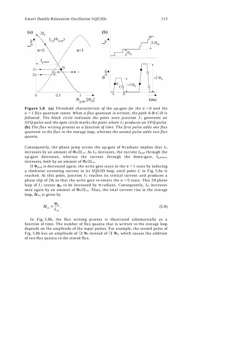
Smart Double Relaxation Oscillation SQUIDs 113
Consequently, the phase jump across the up-gate of π radians implies that Ist
increases by an amount of Φ0/2Lst. As Ist increases, the current Ig,up through theup-gate decreases, whereas the current through the down-gate, Ig,down,increases, both by an amount of Φ0/2Lst.
If Φg,up is decreased again, the write gate stays in the n = 1 state by inducinga clockwise screening current in its SQUID loop, until point C in Fig. 5.8a isreached. At this point, junction J2 reaches its critical current and produces aphase slip of 2π, so that the write gate re-enters the n = 0 state. This 2π phaseleap of J2 causes φup to be increased by π radians. Consequently, Ist increasesonce again by an amount of Φ0/2Lst. Thus, the total current rise in the storageloop, δIst, is given by
δILst
st=
Φ0 . (5.8)
In Fig. 5.8b, the flux writing process is illustrated schematically as afunction of time. The number of flux quanta that is written to the storage loopdepends on the amplitude of the input pulses. For example, the second pulse ofFig. 5.8b has an amplitude of ∼2 Φ0 instead of ∼1 Φ0, which causes the additionof two flux quanta to the stored flux.
Figure 5.8 (a) Threshold characteristic of the up-gate for the n = 0 and then = 1 flux quantum states. When a flux quantum is written, the path A-B-C-D isfollowed. The black circle indicates the point were junction J1 generates anSFQ-pulse and the open circle marks the point where J2 produces an SFQ-pulse.(b) The flux writing process as a function of time. The first pulse adds one fluxquantum to the flux in the storage loop, whereas the second pulse adds two fluxquanta.

Chapter 5114
The function of the down-gate is identical to that of the up-gate, but as thesign of φdown in Eq. (5.7) is opposite to that of φup, flux pulses which are appliedto the down-gate cause a decrease of Ist instead of an increase.
5.3.2 Output range of the Josephson counter
The write gates can only operate properly when the following conditions aresatisfied:
0 0< < < <I I I Ig,up g,max g,down g,maxand , (5.9)
with Ig,max as indicated in Fig. 5.8a. In fact, Ig,max is the critical current of thewrite gates at Φ = (n+½)⋅Φ0, which is, according to Eq. (2.14), equal to
I Ig,maxL,g
L,g=
+⋅
ββ1
2 0 , (5.10)
where I0 represents the critical current of one junction and βL,g is the screeningparameter of the write gates. Using the following circuit equations:
I I Ib,count g,up g,down= + (5.11a)
and
II I
stg,down g,up=
−2
, (5.11b)
the boundary conditions of Eq. (5.9) imply that
II
II
stb,count
g,maxb,count< −
min ,
2 2. (5.12a)
As Ist can have positive and negative values, the peak-to-peak range for Ist isgiven by
( )∆I I I Ist b,count g,max b,count= −min , 2 . (5.12b)
According to Eq. (5.12b), the output range ∆Ist is maximum when Ib,count = Ig,max,in which case ∆Ist = Ig,max.

Smart Double Relaxation Oscillation SQUIDs 115
5.4 Numerical simulations of a smart DROS
Before starting the design and fabrication of the smart DROS, the dynamicbehaviour of the device was investigated by means of numerical simulations.For that purpose, the scheme shown in Fig. 5.9 was implemented in thenumerical simulation program JSIM [20].
The parameter values listed in Fig. 5.9 are typical, with the exception of thevalue of Lst = 50 nH. This small value was chosen to speed up the numericalsimulation process. For the same reason, a DROS with a reference junctioninstead of a reference SQUID was used in the simulations. The time constant ofthe DROS, Lsh/Rsh = 10 ns, implies a relaxation frequency of fRO ≈ 100 MHz. TheLsh-Csq resonances in the DROS are suppressed with a damping resistance ofRd = 30 Ω, giving a damping parameter of D = 2.8 [from Eq. (3.1) ]. The valuesof Min,g = 480 pH and Rin,g = 80 Ω imply an amplitude of ∼2 Φ0 for the fluxpulses applied to the write gates. As Rin,g > Rd, the operation of the DROS is notstrongly influenced by the readout circuitry.
In the preliminary simulations, either Mfb or Min,g was set to zero for adetailed examination of the interaction between the DROS and the Josephsoncounter. Trace (a) of Fig. 5.10 shows the results of a numerical simulation withMfb = 0. The signal flux was varied in time in such a way that Ic,sig > Ic,ref fort < 25 ns and Ic,sig < Ic,ref for t > 25 ns. Consequently, for t < 25 ns, only thereference junction participates in the relaxation oscillations, whereas only thesignal SQUID oscillates for t > 25 ns. As expected, the voltage pulses generated
Figure 5.9 Diagram of the circuit which was used to investigate the dynamicbehaviour of a smart DROS by means of numerical simulations. The inductanceof all SQUIDs is 60 pH, the capacitance of all Josephson junctions is 0.5 pF,and Mfb = Min,g = 480 pH.

Chapter 5116
by the reference junction cause the circulating current in the counter todecrease, whereas the pulses produced by the signal SQUID cause Ist toincrease. As the amplitude of the flux pulses applied to the write gates is ∼2 Φ0,each relaxation oscillation pulse causes the stored flux to increase or decreaseby an amount of 2 Φ0.
Trace (b) of Fig. 5.10 shows a simulation in which Min,g was set to zero,whereas the value of Mfb was restored to 480 pH. The signal flux was varied inthe same way as for trace (a). As Min,g = 0, no flux pulses were applied to thewrite gates in this simulation. Nevertheless, as the relaxation oscillations inthe DROS cause the net flux in the signal SQUID to fluctuate, currentoscillations are induced in the counter via the mutual inductance between thesignal SQUID and the feedback coil. These oscillations of Ist “reflect” therelaxation oscillations in the DROS.
Figure 5.10 Numerical simulations of the circuit in Fig. 5.9 for three differentsets of parameters. Vref is the voltage across the reference junction of the DROS,Vsig is the voltage across the signal SQUID, Ist is the circulating current in thestorage loop and Φst = Lst⋅Ist represents the stored flux. The signal flux wasvaried in such a way that Ic,sig > Ic,ref for t < 25 ns and Ic,sig < Ic,ref for t > 25 ns.Trace (a): Mfb = 0, Rd,fb = ∞, Min,g = 480 pH. Trace (b): Mfb = 480 pH, Rd,fb = ∞,Min,g = 0. Trace (c): Mfb = 480 pH, Rd,fb = 30 Ω, Min,g = 0. The other parametersare indicated in Fig. 5.9.

Smart Double Relaxation Oscillation SQUIDs 117
When the reference junction oscillates, the relaxation oscillations inducesmooth current fluctuations in the counter. However, when the signal SQUIDoscillates, large current spikes are induced in the counter when the signalSQUID switches from the superconducting state to the normal state and viceversa. These spikes, which could possibly degrade the operation of the counter,can be reduced by shunting the feedback coil with a damping resistor Rd,fb, asshown in Fig. 5.9. For high frequencies, Rd,fb constitutes a lower impedancethan the storage inductor, and therefore the current spikes will flow throughRd,fb rather than through the counter inductance. To prevent phase shifts in thefeedback loop, the value of Rd,fb has to be such that the time constant Lfb/Rd,fb ismuch smaller than 1/fRO. Furthermore, the additional flux noise due to theJohnson noise generated by Rd,fb, √SΦ = Mfb⋅√(4kBT/Rd,fb), should be negligiblecompared to the intrinsic noise of the DROS. Trace (c) of Fig. 5.10 shows anumerical simulation with the same parameters as for trace (b), but now withRd,fb = 30 Ω. As expected, the current spikes in the counter are stronglysuppressed by the addition of Rd,fb.
Figure 5.11 Numerical simulation of the response of a smart DROS tovariations of the input flux. Vref is the voltage across the reference junction of theDROS, Vsig is the voltage across the signal SQUID, Ist is the circulating currentin the storage loop and Φfb = Mfb⋅Ist represents the feedback flux.Simulation parameters: Min,g = Mfb = 480 pH, Rd,fb = 30 Ω, other parameters asindicated in Fig. 5.9.

Chapter 5118
Figure 5.11 shows a numerical simulation of a smart DROS in operation.Initially, the system is in its dynamic equilibrium, and the reference junctionand the signal SQUID pulse alternately. Consequently, the current in thecounter oscillates around an average value. At t = 100 ns, a flux step of 0.2 Φ0 isapplied, disturbing the dynamic equilibrium of the system. As a result, only thesignal SQUID produces voltage pulses, causing the circulating current in thecounter - and accordingly the feedback flux - to increase steadily until thesystem has established a new dynamic equilibrium. At t = 300 ns, a flux step of-0.4 Φ0 is applied and now only the reference SQUID generates pulses in orderto restore the dynamic equilibrium.
The simulations in Fig. 5.11 show that the output of the smart DROS tracksthe input flux, which indicates proper operation.
5.5 Experimental investigation of the Josephsoncounter
The numerical simulations in the previous section show that, in theory, theconstruction of a smart DROS based on a Josephson counter is possible. Beforedesigning and constructing a fully integrated smart DROS, we first developed aprototype of the Josephson counter to investigate its characteristics. This isdescribed in the present section.
5.5.1 Chip layout of the Josephson counters
For an experimental investigation of the Josephson counter, devices like theone shown in Fig. 5.12 have been designed, fabricated and characterized. Thedevices were fabricated with our standard Nb/AlOx thin film process, having aminimum feature size of 4 µm.
The write gates are non-hysteretic washer-type dc SQUIDs, each with a10-turns input coil. The hole size of the washers, 20 µm, corresponds to aninductance of 32 pH. The actual SQUID inductance was measured to beLsq,g ≈ 75 pH (βL,g ≈ 2.2), which is about twice the hole inductance, probably dueto the parasitic inductance of the slit. The mutual inductance between theinput coils and the write gates was measured to be Min,g ≈ 480 pH. The criticalcurrent of the 4 x 4 µm2 Josephson junctions is I0 ≈ 30 µA and the experimentalvalue of the shunt resistor across the junctions is 1.5 Ω. With the assumedjunction capacitance of 0.5 pF, these parameters yield βC ≈ 0.1, which impliesnon-hysteretic junction behaviour.
The storage inductor, having a design value of 600 nH, is composed of fourtwo-layer multi-turn coils of the same type that was used in early DROSexperiments [21,22]. The coils are arranged “gradiometrically” in order tominimize the sensitivity to external noise. This configuration also reduces themagnetic stray fields produced by the storage inductor.

Smart Double Relaxation Oscillation SQUIDs 119
The circulating current in the storage loop was measured with an additionalnon-hysteretic dc SQUID, the readout SQUID, located in the “down-branch” ofthe counter. The additional inductance due to the input coil of this readoutSQUID (∼5 nH) is negligible in comparison with the other inductances in thestorage loop. The parameters of the readout SQUID are equal to those of thewrite gates. The current Ig,down can be calculated from Ig,down = Φread/Min,read,where Φread represents the flux which is induced in the readout SQUID, andMin,read ≈ 480 pH is the mutual inductance between the readout SQUID and itsinput coil. A single-turn feedback coil around the readout SQUID was used forflux locked loop operation.
5.5.2 Characterization of the Josephson counters
Four Josephson counters were tested by applying flux pulses, generated by twofunction generators, to the write gates. To reduce the influence ofenvironmental electromagnetic noise, the counters were enclosed in a Nbshield. Moreover, all wires between the room temperature environment and theJosephson counters were low pass filtered in order to prevent radio frequencyinterference (RFI).
Figure 5.12 (a) Micrograph and (b) scheme of the prototype of the Josephsoncounter. The actual area shown in figure (a) is approximately 1.0 x 1.7 mm2.

Chapter 5120
The readout SQUID was operated with the DROS flux locked loopelectronics of Fig. 4.5. Due to its small flux-to-voltage transfer of ∼100 µV/Φ0,the sensitivity of the readout SQUID was amplifier limited, but this is not animportant issue in the present experiments.
The measured response to flux pulses which were applied to the up-gate isshown in Fig. 5.13. The pulses, with a peak-to-peak amplitude of ∼24 Φ0, wereapplied at a frequency of about 5 Hz. Trace (a) was recorded for Ib,count = 0, andrepresents the direct crosstalk between Φg,up and the readout SQUID. Trace (b)was measured at Ib,count = 39 µA. By subtracting trace (a) from trace (b), the“parasitic” crosstalk effect was excluded, as shown by trace (c). The latter traceshows a clear correspondence with the model of Fig. 5.8b. If flux pulses wereapplied to the down-gate, Ist decreased instead of increased at each pulse. Thesemeasurements indicate that the counters operate as expected.
Figure 5.14 shows the measured response of a counter when pulse trains of∼1800 flux pulses were applied alternately to the up-gate and to the down-gate.The peak-to-peak amplitude of the flux pulses was ∼1 Φ0 for trace (a), ∼2 Φ0 fortrace (b) and ∼3 Φ0 for trace (c). Consequently, the gates wrote respectively one,two or three flux quanta to the storage loop at each pulse. From the amplitudes
Figure 5.13 Experimental response of a Josephson counter to flux pulses at theup-gate. Trace (a) was measured at Ib,count = 0 µA and trace (b) at Ib,count = 39 µA.Trace (c) gives the difference between trace (b) and trace (a). The vertical offsetsare arbitrary.

Smart Double Relaxation Oscillation SQUIDs 121
of the traces [5.1 µA for trace (a), 10.0 µA for trace (b) and 15.1 µA fortrace (c) ], the value of Lst was determined to be Lst = 750 nH (±10%). Two of theinvestigated Josephson counters showed a much lower value for Lst, which wasattributed to electrical shorts in the two-layer multi-turn storage inductors.
For determination of the output range of the counters, ∆Ist, the number ofapplied flux pulses was increased until the current in the storage loopsaturated, as is illustrated by the measurements in Fig. 5.15a.
Figure 5.15b shows the measured values of ∆Ist as a function of Ib,count. Forthis particular device, the critical current of the Josephson junctions was∼45 µA instead of 30 µA. The solid line in Fig. 5.15b is a fit according toEq. (5.12b), using Ig,max = 75 µA. This fit value is in good agreement with thetheoretical expectation of 70 µA, obtained from Eq. (5.10). Obviously, theexperimental relation between ∆Ist and Ib,count is well described by Eq. (5.12b).
Figure 5.14 Experimental response of a Josephson counter to pulse trains of∼1800 pulses each, applied alternately to the up-gate and to the down-gate. Theamplitude of the applied flux pulses was about 1 Φ0 for trace (a), 2 Φ0 fortrace (b) and 3 Φ0 for trace (c). The counter bias current was Ib,count = 30 µA forall traces. The vertical offsets are arbitrary.

Chapter 5122
5.6 Experimental investigation of the smart DROS
Using the theoretical results of section 5.4 and the experimental results ofsection 5.5, an integrated smart DROS was designed. This fully operationalprototype is discussed in this section.
5.6.1 Design of the smart DROS
A micrograph and the scheme of the fabricated smart DROSs are presented inFig. 5.16a (page 124) respectively Fig. 5.16b (page 125). The main parametersof the device are listed next to Fig. 5.16b. The devices, having a minimumfeature size of 4 µm, were fabricated using our standard Nb/AlOx thin filmprocess. For testing purposes, also separate elements of the smart DROS, suchas the DROS, the Josephson counter or the readout SQUID, were fabricated onthe same wafer as the compound devices.
Figure 5.15 (a) Experimental response of a Josephson counter to pulse trains,applied alternately to the up-gate and to the down-gate, at a counter biascurrent of Ib,count = 15 µA. The number of flux pulses was sufficiently large tosaturate the current in the storage loop. The positive and negative saturationlevels are indicated by the horizontal dashed lines. (b) Peak-to-peak outputrange as a function of the applied bias current. The solid line is a fit accordingto Eq. (5.12b). The maximum value of ∆Ist = 75 µA corresponds to a flux changeof ∼2.5⋅104 Φ0 in the storage loop.
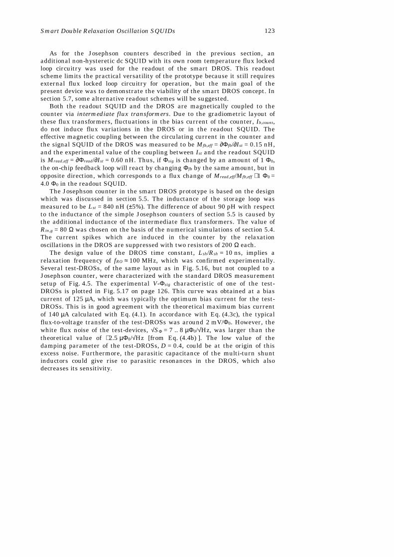
Smart Double Relaxation Oscillation SQUIDs 123
As for the Josephson counters described in the previous section, anadditional non-hysteretic dc SQUID with its own room temperature flux lockedloop circuitry was used for the readout of the smart DROS. This readoutscheme limits the practical versatility of the prototype because it still requiresexternal flux locked loop circuitry for operation, but the main goal of thepresent device was to demonstrate the viability of the smart DROS concept. Insection 5.7, some alternative readout schemes will be suggested.
Both the readout SQUID and the DROS are magnetically coupled to thecounter via intermediate flux transformers. Due to the gradiometric layout ofthese flux transformers, fluctuations in the bias current of the counter, Ib,count,do not induce flux variations in the DROS or in the readout SQUID. Theeffective magnetic coupling between the circulating current in the counter andthe signal SQUID of the DROS was measured to be Mfb,eff = ∂Φfb/∂Ist = 0.15 nH,and the experimental value of the coupling between Ist and the readout SQUIDis Mread,eff = ∂Φread/∂Ist = 0.60 nH. Thus, if Φsig is changed by an amount of 1 Φ0,the on-chip feedback loop will react by changing Φfb by the same amount, but inopposite direction, which corresponds to a flux change of Mread,eff/Mfb,eff ⋅ 1 Φ0 =4.0 Φ0 in the readout SQUID.
The Josephson counter in the smart DROS prototype is based on the designwhich was discussed in section 5.5. The inductance of the storage loop wasmeasured to be Lst = 840 nH (±5%). The difference of about 90 pH with respectto the inductance of the simple Josephson counters of section 5.5 is caused bythe additional inductance of the intermediate flux transformers. The value ofRin,g = 80 Ω was chosen on the basis of the numerical simulations of section 5.4.The current spikes which are induced in the counter by the relaxationoscillations in the DROS are suppressed with two resistors of 200 Ω each.
The design value of the DROS time constant, Lsh/Rsh = 10 ns, implies arelaxation frequency of fRO ≈ 100 MHz, which was confirmed experimentally.Several test-DROSs, of the same layout as in Fig. 5.16, but not coupled to aJosephson counter, were characterized with the standard DROS measurementsetup of Fig. 4.5. The experimental V-Φsig characteristic of one of the test-DROSs is plotted in Fig. 5.17 on page 126. This curve was obtained at a biascurrent of 125 µA, which was typically the optimum bias current for the test-DROSs. This is in good agreement with the theoretical maximum bias currentof 140 µA calculated with Eq. (4.1). In accordance with Eq. (4.3c), the typicalflux-to-voltage transfer of the test-DROSs was around 2 mV/Φ0. However, thewhite flux noise of the test-devices, √SΦ = 7 .. 8 µΦ0/√Hz, was larger than thetheoretical value of ∼2.5 µΦ0/√Hz [from Eq. (4.4b) ]. The low value of thedamping parameter of the test-DROSs, D = 0.4, could be at the origin of thisexcess noise. Furthermore, the parasitic capacitance of the multi-turn shuntinductors could give rise to parasitic resonances in the DROS, which alsodecreases its sensitivity.
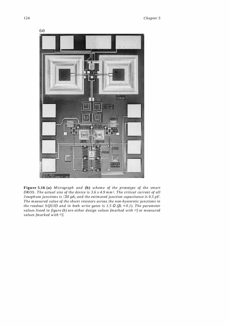
Chapter 5124
Figure 5.16 (a) Micrograph and (b) scheme of the prototype of the smartDROS. The actual size of the device is 3.6 x 4.9 mm2. The critical current of allJosephson junctions is ∼30 µA, and the estimated junction capacitance is 0.5 pF.The measured value of the shunt resistors across the non-hysteretic junctions inthe readout SQUID and in both write gates is 1.5 Ω (βC ≈ 0.1). The parametervalues listed in figure (b) are either design values [marked with a)] or measuredvalues [marked with b)].
Smart Double Relaxation Oscillation SQUIDs 125

Chapter 5126
5.6.2 Operation of the smart DROS
Four smart DROSs were characterized experimentally. The devices wereshielded from external noise sources by means of a superconducting Nbshielding, and all electrical connections between the room temperatureelectronics and the smart DROSs were low pass filtered for RFI suppression.The readout SQUID was operated in a simple flux locked loop without fluxmodulation.
In Fig. 5.18a, the transfer function of one of the smart DROSs is shown fornine different values of Ib,count. The settings of the DROS, Φref and Ib,dros, werenot changed for the different traces. The horizontal axis of Fig. 5.18a shows theapplied signal flux, Φsig, and the vertical axis gives the resulting flux in thereadout SQUID, Φread. The linear relation between Φsig and Φread clearly showsthat the device works according to the theory of section 5.4.
As discussed in section 5.3.2, the output range of the Josephson counterdepends on the value of Ib,count. For the device in Fig. 5.18, the operation rangeincreased linearly with Ib,count until Ib,count ≈ 50 µA. Above that value, the outputrange of the Josephson counter decreased again, cf. Fig. 5.15b. AtIb,count = 50 µA, the smart DROS showed a linear response over a Φsig range ofalmost 3 Φ0.
The slope of the characteristics in Fig. 5.18a is ∂Φread/∂Φsig = 3.9. Averagedover the four characterized devices, the value of ∂Φread/∂Φsig was<∂Φread/∂Φsig> = 3.95, with a maximum deviation of ±2%. This is in goodagreement with the value of Mread,eff/Mfb,eff = 4.0.
Figure 5.17 Experimental V-Φsig characteristic of one of the test-DROSs at abias current of Ib,dros = 125 µA.

Smart Double Relaxation Oscillation SQUIDs 127
To investigate the linearity of the system, the local slope ∂Φread/∂Φsig of thecharacteristics in Fig. 5.18a was measured by superposing a sinusoidal signalwith a frequency of 500 Hz and an amplitude of ∼0.01 Φ0 on the slow (∼0.1 Hz)sweep of Φsig. With an analogue lock-in amplifier [23], the amplitude of theresulting 500 Hz fluctuation of Φread, which is proportional to ∂Φread/∂Φsig, wasmeasured. Figure 5.18b shows the experimental results for several values of
Figure 5.18 (a) Experimental transfer function of a smart DROS for differentvalues of Ib,count. The horizontal axis displays the applied signal flux, and thevertical axis gives the resulting flux in the readout SQUID. (b) The slope∂Φread/∂Φsig of some of the characteristics in figure (a).

Chapter 5128
Ib,count. For each bias current, the value of ∂Φread/∂Φsig at the plateau is constantwithin a relative range of ±2.5%. As the traces in Fig. 5.18b did not showhysteresis when the sweep direction of Φsig was changed, motion of pinned fluxis not likely to be the mechanism behind the small fluctuations of ∂Φread/∂Φsig.Probably, the parasitic magnetic coupling between the different elements of thesmart DROS is the malefactor.
Trace (a) of Fig. 5.19 shows the experimental flux noise spectrum of one ofthe characterized devices. The white flux noise level of √SΦ,sig ≈ 6.5 µΦ0/√Hzcorresponds to an energy sensitivity of ε ≈ 2000 h. As a result of the non-modulated flux locked loop configuration, the readout SQUID has a rather highwhite flux noise level of ∼16 µΦ0/√Hz. Taking into account the flux gain of 4.0,this corresponds to a contribution of 4 µΦ0/√Hz to the overall flux noise, asplotted in trace (b) of Fig. 5.19. Subtracting the noise of the readout SQUIDfrom the total flux noise, the intrinsic flux noise level of the smart DROS wasdeduced to be ∼5 µΦ0/√Hz (εintr ≈ 1150 h).
Trace (c) of Fig. 5.19 shows the flux noise of the same DROS, but nowoperated in a conventional flux locked loop at room temperature. For thismeasurement, the DROS and the counter were disconnected by scratching theresistors Rin,g mechanically. The measured white flux noise, 7 µΦ0/√Hz, isalmost identical to the overall flux noise (∼6.5 µΦ0/√Hz), and somewhat abovethe intrinsic flux noise (∼5 µΦ0/√Hz) of the smart DROS. Thus, the intrinsicflux noise of the DROS in the smart configuration is even better than in theconventional configuration. The reason could be that the resistors Rin,g, which
Figure 5.19 Flux noise spectra of the smart DROS.

Smart Double Relaxation Oscillation SQUIDs 129
are connected parallel to the damping resistors Rd of the DROS, increase thevalue of the damping parameter from D = 0.4 in the conventional scheme toD = 1.6 in the smart configuration.
The bandwidth and the slew rate of the smart DROS prototype could not bedetermined, since these performance parameters were limited by the fluxlocked loop circuitry of the readout SQUID, having a bandwidth of about20 kHz.
5.7 Discussion and conclusions
The results in the previous section prove that the smart DROS works inpractice as well as in theory. The energy sensitivity of the presented prototype,ε ≈ 2000 h (εintr ≈ 1150 h), is better than that of the Fujitsu single-chip SQUIDalmost by a factor of two [13]. However, the prototype still needs some fine-tuning to become a device of real practical value.
For instance, the relaxation frequency can be increased to ∼1 GHz in orderto increase the sensitivity, the bandwidth and the slew rate. Furthermore, anew design for the storage inductor and the intermediate flux transformers canimprove the dynamic range of the device considerably. Two last examples ofpotential improvements are the replacement of the single-turn input coil of theDROS by a multi-turn input coil for efficient coupling with the outside worldand the implementation of a reference junction instead of a reference SQUID toreduce the number of wires.
However, all these modifications do not eliminate the bottleneck of theprototype: the readout SQUID, which still requires flux locked loop circuitry atroom temperature. Because of this readout SQUID, the initial aim of the smartDROS, operation without external flux locked loop electronics, has not beenaccomplished yet. Some alternative readout schemes to get around thissituation will be discussed below.
The smart DROS could for instance be read out in the same way as theFujitsu single-chip SQUID by counting the output voltage pulses of the DROSwith a room temperature bi-directional counter. With this readout system, avery large dynamic range can be realized when the flux transformer circuit isused as the counter inductance [4]. However, as in the case of frequency readoutof a ROS, cryogenic pre-amplification of the voltage pulses, for instance with ahigh electron mobility transistor (HEMT) [5,24], might be necessary in this case.Furthermore, coaxial transmission lines between the cryogenic environmentand the digital counter at room temperature would be required, whichintroduces a serious heat load problem in multi-channel systems. Therefore,this readout scheme is especially appropriate for applications which require alarge measurement bandwidth and a large dynamic range, but only a fewchannels.
As mentioned in the introduction of section 5.3, the counter of the smartDROS can also be implemented with semiconductor electronics. In ref. [19], for

Chapter 5130
instance, a cryogenic 12 bit digital counter based on conventional CMOSintegrated circuits is presented. A smart DROS based on such asemiconducting counter would generate an output voltage depending linearlyon the input flux. As it is not straightforward to integrate the superconductingand the semiconducting elements of such a “hybrid” smart DROS on a singlechip, it would consist of several discrete components, which increases thesystem complexity. However, the number of wires between the environmentand the SQUIDs in a multi-channel system could be reduced drastically withthis configuration, which is a large advantage. Moreover, for low signalfrequencies, as for instance in bio-magnetic applications, simple wires insteadof coaxial lines would suffice for the readout of a “hybrid” smart DROS.
Further development of the smart DROS, following the recommendationsabove, offers the perspective of a very sensitive, fast and versatile SQUIDsensor.
References1 N. Fujimaki, “Josephson integrated circuits III. A single-chip SQUID magnetometer”,
Fujitsu Sci. Tech. J. 27, 59-83 (1991).2 http://www.hypres.com/~masoud/digital.shtml3 N. Fujimaki, H. Tamura, T. Imamura and S. Hasuo, “A single-chip SQUID magnetometer”,
IEEE Trans. Electron Devices 35, 2412-2418 (1988).4 M. Radparvar, “A wide dynamic range single-chip SQUID magnetometer”, IEEE Trans.
Appl. Supercond. 4, 87-91 (1994).5 U. Fath, R. Hundhausen, T. Fregin, P. Gerigk and W. Eschner, “Experimental digital
SQUID with integrated feedback circuit”, IEEE Trans. Appl. Supercond. 7, 2747-2751(1997).
6 S.V. Rylov, “Analysis of high-performance counter-type A/D converters using RSFQlogic/memory elements”, IEEE Trans. Magn. 27, 2431-2434 (1991).
7 K. Gotoh, N. Fujimaki, H. Suzuki, T. Imamura, S. Hasuo and A. Shibatomi, “Multichannelsingle-chip SQUID with a Josephson multiplexer”, Supercond. Sci. Technol. 4, 610-612(1991).
8 K. Gotoh, N. Fujimaki, T. Imamura and S. Hasuo, “8-channel array of single-chip SQUIDsconnection to Josephson multiplexer”, IEEE Trans. Appl. Supercond. 3, 2601-2604 (1993).
9 Fujitsu Laboratories Ltd., 10-1 Morinosato-Wakamiya, Atsugi 243-01, Japan.10 K.K. Likharev and V.K. Semenov, “RSFQ logic/memory family: a new Josephson-junction
technology for sub-terahertz-clock-frequency digital systems”, IEEE Trans. Appl.Supercond. 1, 3-28 (1991).
11 V.K. Semenov and J.A. Polyakov, “Fully integrated digital SQUID”, in abstract book 3rd
European Conference on Applied Superconductivity (EUCAS), abstract no. 10Ge-70,Veldhoven, the Netherlands (1997).
12 N. Fujimaki, H. Tamura, T. Imamura and S. Hasuo, “Thermal noise-limited sensitivity ofthe pulse-biased SQUID magnetometer”, J. Appl. Phys. 65, 1626-1630 (1989).
13 N. Fujimaki, K. Gotoh, T. Imamura and S. Hasuo, “Thermal-noise-limited performance insingle-chip superconducting quantum interference devices”, J. Appl. Phys. 71, 6182-6188(1992).
Smart Double Relaxation Oscillation SQUIDs 131
14 R.H. Koch, J. Clarke, J.M. Martinis, W.M. Goubau, C.M. Pegrum and D.J. van Harlingen,“Investigation of 1/f noise in tunnel junction dc SQUIDs”, IEEE Trans. Magn. 19, 449-452(1983).
15 M. Radparvar and S.V. Rylov, “High sensitivity digital SQUID magnetometers”, IEEETrans. Appl. Supercond. 7, 3682-3685 (1997).
16 P.F. Yuh and S.V. Rylov, “An experimental digital SQUID with large dynamic range andlow noise”, IEEE Trans. Appl. Supercond. 5, 2129-2132 (1995).
17 M. Radparvar and S. Rylov, “An integrated digital SQUID magnetometer with highsensitivity input”, IEEE Trans. Appl. Supercond. 5, 2142-2145 (1995).
18 HYPRES Inc., 175 Clearbrook Road, Elmsford, NY 10523, U.S.A.19 E. Crocoll, H. Matz, M. Reick and W. Jutzi, “Digital CMOS circuits below 100 K”, in
Superconducting Devices and Their Applications, ed. H. Koch and H. Lübbig, SpringerProceedings in Physics 64, Springer-Verlag, Berlin / Heidelberg, 362-365 (1992).
20 Simulation software: JSIM 2.1, developed by E.S. Fang, University of California, Berkeley,CA 94720, U.S.A.
21 D.J. Adelerhof, Second generation dc SQUID magnetometers: (Double) RelaxationOscillation SQUIDs, Ph.D. thesis University of Twente, Enschede (1993).
22 D.J. Adelerhof, H. Nijstad, J. Flokstra and H. Rogalla, “Relaxation oscillation SQUIDs withhigh ∂V/∂Φ”, IEEE Trans. Appl. Supercond. 3, 1862-1865 (1993).
23 Princeton Applied Research model PAR 124.24 G. Fontana, R. Mezzena, S. Vitale, M. Cerdonio, M. Mück, G. Hallmanns and C. Heiden,
“Improved sensitivity of planar microwave biased rf SQUIDs using a cryogenic HEMTpreamplifier”, IEEE Trans. Appl. Supercond. 3, 1820-1823 (1993).

132

133
Summary
This thesis describes the development of low Tc superconducting quantuminterference devices (SQUIDs) based on the relaxation oscillation principle.SQUIDs are the most sensitive magnetic flux sensors available nowadays. Asthey can detect very accurately any physical quantity that can be converted toa magnetic flux, their field of applications is wide-ranging. Examples ofapplications are the detection of the tiny magnetic fields generated by thehuman brain, the measurement of voltages in the picovolt range and thereadout of cryogenic particle detectors.
A dc SQUID consists of a superconducting loop which is interrupted by twoJosephson junctions. These Josephson junctions constitute a weak link betweenthe superconducting wave functions in both parts of the SQUID loop. Due tointerference of these wave functions, the voltage across a current biaseddc SQUID is modulated by the magnetic flux which is applied to the SQUIDloop. The flux versus voltage characteristic of a dc SQUID is periodic with aperiod equal to the flux quantum, Φ0 = 2.07⋅10-15 Wb. For most applications, thenon-linear flux-to-voltage transfer function is linearized by using the SQUID asa null detector in a feedback loop, the so-called flux locked loop.
Most contemporary low Tc dc SQUIDs are based on thin film Josephsontunnel junctions, which consist of two superconducting electrodes, separated bya thin (∼1 nm) insulating barrier. Due to the intrinsic capacitance of thesetunnel junctions, their current versus voltage characteristics are hysteretic.Usually, this hysteresis is removed with external resistive shunts across thejunctions. These resistors limit the maximum slope of the flux-to-voltagecharacteristic to a typical value of ∂V/∂Φ = 100 µV/Φ0. Consequently, the typicalflux noise level of a dc SQUID, √SΦ = 1 µΦ0/√Hz, corresponds to a voltage noiseof √SV ≈ 0.1 nV/√Hz at the output. Since this is about one order of magnitudebelow the input noise of present room temperature amplifiers, direct voltage

134
readout would reduce the sensitivity considerably. Usually, amplifier limitationof the sensitivity is avoided with flux modulation techniques and resonantcryogenic impedance matching circuitry. Especially in multi-channel systems,incorporating hundreds of dc SQUIDs, such modulated readout schemes havedisadvantages, such as crosstalk between adjacent channels, the complexconstruction of the system and the associated high production costs. Moreover,the modulation frequency, 100 to 500 kHz for most commercial systems,constrains the measurement bandwidth.
The relaxation oscillation SQUID (ROS) and the double relaxationoscillation SQUID (DROS) have been developed to enable simpler, non-modulated readout techniques, thus avoiding the drawbacks of theconventional flux locked loop configuration. The principle of operation of these“second generation” dc SQUIDs is based on relaxation oscillations which areinduced in hysteretic dc SQUIDs by an external shunt, consisting of aninductor L and a resistor R in series.
In a ROS, this external L-R circuit shunts a single hysteretic dc SQUID. If aROS is biased with an appropriate dc bias current, the relaxation oscillationprocess generates voltage pulses with a typical amplitude of 1 mV. Thefrequency of these pulses depends on the critical current of the hystereticdc SQUID, which itself depends on the applied magnetic flux. Therefore, a ROSis a flux-to-frequency converter. ROSs can also be used as flux-to-voltagetransducers, but the flux-to-voltage transfer coefficient of a ROS is typically ofthe same order as that of conventional resistively shunted dc SQUIDs.Therefore, voltage readout of a ROS has no significant advantages comparedwith voltage readout of a conventional dc SQUID.
Theoretically, the sensitivity of a ROS is limited by the thermal noise on thecritical current of the hysteretic dc SQUID. The sensitivity improves if therelaxation frequency is increased, but as soon as the relaxation frequencyexceeds ∼1% of the plasma frequency of the Josephson junctions, interferencebetween the relaxation oscillations and the plasma oscillations impedes furtherimprovement of the sensitivity. Therefore, the optimum relaxation frequency isabout 1 GHz for most practical devices. At this relaxation frequency, thetheoretical noise performance of a ROS matches that of standard dc SQUIDs.
For ROSs operating at frequencies in the GHz range, parasitic L-Cresonances between the shunt inductor and the capacitance of the Josephsonjunctions can seriously degrade the performance. Such parasitic resonances canbe suppressed with an additional damping resistor.
Several ROSs with different parameters have been investigatedexperimentally. These ROSs were not equipped with multi-turn input coils. Theflux versus frequency characteristics of the devices were measured at variousvalues of the bias current. The highest observed relaxation frequency was∼7 GHz; higher frequencies could not be detected due to the noise of the readoutamplifier at room temperature. The experimental characteristics were

Summary 135
successfully fitted with a simple model, and the values of the fit parameterswere in close agreement with the theoretical expectation.
The ROSs were also operated in a flux locked loop with frequency readout.The best measured white flux noise was √SΦ = 2.5 µΦ0/√Hz, which correspondsto an energy resolution of ε ≈ 600 h. This energy sensitivity exceeds thetheoretical value by two orders of magnitude, which discrepancy is probablycaused by the non-ideal FM demodulator which was used for the flux lockedloop experiments. The application of a cryogenic high frequency pre-amplifiercould possibly improve the flux locked loop performance, but this would lead toa rather complex readout configuration.
DROSs are used with voltage readout instead of frequency readout. Their largeflux-to-voltage transfer coefficient enables direct voltage readout with a roomtemperature amplifier without degradation of the sensitivity. In a DROS, twohysteretic dc SQUIDs in series, the signal SQUID and the reference SQUID,are shunted by an external L-R circuit. The signal flux is applied to the signalSQUID, whereas a constant flux is applied to the reference SQUID in order totune its critical current to a fixed value. Depending on the value of the signalflux, either the signal SQUID or the reference SQUID participates in therelaxation oscillations, while the other SQUID remains superconducting.
The maximum flux-to-voltage transfer coefficient of a DROS is determinedby the thermal spread on the critical currents of both SQUIDs, a typical valuefor practical devices is ∂V/∂Φ ≈ 1 mV/Φ0. As for a ROS, the sensitivity of aDROS improves at increasing relaxation frequencies. At relaxation frequenciesexceeding ∼1% of the plasma frequency, interactions between the plasmaoscillations and the relaxation oscillations limit the flux-to-voltage transfercoefficient and the sensitivity of a DROS, which implies an optimum relaxationfrequency of ∼1 GHz for most practical devices. At this frequency, thesensitivity of a DROS is comparable to that of a conventional dc SQUID.
Several measurement systems based on DROSs are discussed in this thesis.A three-channel first-order gradiometer system with wire-wound pickup coilswas constructed in order to investigate the applicability of DROSs in multi-channel magnetometer systems. The white magnetic field noise of this system,4 fT/√Hz (∼10 fT/√Hz @ 1 Hz), did not change when the three channels wereoperated simultaneously. This demonstrates that interference of the relaxationoscillations in adjacent DROSs does not play a significant role in multi-channelsystems, which makes the DROS a promising device for use in large bio-magnetic systems.
Using the experience acquired with this three-channel gradiometer system,improved DROSs were designed, fabricated and characterized. In order toreduce the direct pickup of magnetic fields, the signal SQUIDs of these newDROSs had a gradiometric “figure-8” configuration. Another innovation wasthe substitution of the reference SQUID by a single reference junction. In thisway, the number of wires between the DROS and the room temperatureelectronics could be decreased by two. The white flux noise of the devices with a

136
reference junction, 6 µΦ0/√Hz (ε ≈ 200 h), was only slightly larger than that ofthe devices with a reference SQUID, 5 µΦ0/√Hz (ε ≈ 150 h). Connected to anexternal planar first-order gradiometer with pickup coils of 2 x 2 cm2, thedevices reached a magnetic field sensitivity better than 2 fT/√Hz (∼10 fT/√Hz@ 1 Hz) inside a magnetically shielded room, which is amply sufficient for awide variety of bio-magnetic experiments. The gradiometric DROSs were alsoused as very sensitive current sensors with a resolution of 2 pA/√Hz. Thisapplication was demonstrated by recording the subgap current versus voltagecharacteristics of a voltage biased tunnel junction at temperatures between1.6 K and 4.2 K.
In order to increase the effective pickup area without using an external fluxtransformer, a directly coupled eight-loop DROS magnetometer was developed.Owing to the multi-loop structure of the signal SQUID, a relatively largeeffective pickup area of 4.1 mm2 could be realized with a moderate SQUIDinductance of 410 pH. However, due to the Johnson noise generated in thedamping resistors, the flux-to-voltage transfer coefficient of the directly coupleddevices was limited to 280 µV/Φ0. As a direct consequence of this moderatetransfer, the magnetic field sensitivity of the multi-loop DROS magnetometerwas restricted to 7 fT/√Hz due to the noise of the room temperature readoutamplifier.
The pulsed output signal of a DROS is particularly suited for digital readout. Ina digital or “smart” DROS, the voltage pulses produced by the signal SQUIDand the reference SQUID drive a bi-directional digital counter whose outputsupplies the feedback flux to keep the DROS flux locked. Thus, the role of thedigital counter is comparable to that of the integrator in the conventional fluxlocked loop configuration.
Especially when the counter and the DROS are integrated on a single chip,the smart DROS configuration can lead to a simpler readout scheme, requiringfor instance less wires between the cryogenic environment and roomtemperature. Unlike other types of digital SQUIDs, the smart DROS does notneed an external clock for operation, because the relaxation oscillationsconstitute an internal clock. Therefore, a smart DROS can work at highfrequencies, which makes it potentially a very fast sensor.
A prototype of the smart DROS has been designed, fabricated andcharacterized. The bi-directional counter in this prototype is based on a so-called Josephson counter, consisting of a superconducting storage loop and twowrite gates. These write gates, which are driven by the voltage pulsesgenerated by the DROS, can add flux quanta to or remove flux quanta from thequantized flux in the storage loop. The circulating current in the storage loopgenerates the feedback flux for the DROS via a flux transformer. For readout ofthe Josephson counter, an additional resistively shunted dc SQUID, coupled tothe circulating current in the counter by means of a second flux transformer,was included in the design. This readout SQUID was operated in a flux lockedloop with room temperature electronics. Of course, this readout configuration

Summary 137
limits the versatility of the prototype considerably, but the main goal of thepresent experiments was to demonstrate the feasibility of the smart DROSconcept.
The smart DROS prototype, having a relaxation frequency of ∼100 MHz,worked properly and its response was linear over an input flux range of ∼3 Φ0.The bandwidth and the maximum slew rate of the prototype were limited bythe external flux locked loop circuitry of the readout SQUID. The flux noise ofthe device, 6.5 µΦ0/√Hz (ε ≈ 2000 h) including the noise of the readout SQUIDand 5 µΦ0/√Hz (ε ≈ 1150 h) excluding the noise of the readout SQUID, was evenbetter than the noise level of 7 µΦ0/√Hz which was measured for the sameDROS, operated in a conventional instead of a “smart” flux locked loop.
These promising results encourage further development of the smart DROS.An example of a new development could be the replacement of thesuperconducting Josephson counter by a cryogenic semiconducting circuit.Such improved smart DROSs can for instance be used in large multi-channelSQUID systems - e.g. for bio-magnetic measurements - or in applicationsrequiring a wide measurement bandwidth, such as the readout of cryogenicparticle detectors.

138

139
Samenvatting (Summary in Dutch)
Dit proefschrift beschrijft de ontwikkeling van lage-Tc SQUIDs die gebaseerdzijn op het relaxatie oscillatie principe. Het woord SQUID is een acroniem voorhet Engelse Superconducting QUantum Interference Device. SQUIDs zijn degevoeligste sensoren voor magnetische flux die momenteel bestaan. Omdat zeiedere fysische grootheid die naar magnetische flux is te “vertalen” met groteprecisie kunnen meten hebben ze een breed toepassingsgebied. Voorbeeldenvan toepassingen zijn de detectie van de zeer kleine magnetische velden dieworden gegenereerd door menselijke hersenen of andere organen, het metenvan elektrische spanningen in het picovoltbereik en de uitlezing van cryogenedeeltjesdetectors.
Een dc SQUID bestaat uit een supergeleidende ring die op twee plaatsen isonderbroken door een Josephson junctie. Deze Josephson juncties vormen eenzwakke koppeling tussen de supergeleidende golffuncties in beide delen van dering, waardoor interferentie mogelijk is. Ten gevolge van deze interferentie isde elektrische spanning over een stroom-gebiast dc SQUID afhankelijk van demagnetische flux die wordt omsloten door de SQUID-ring. De flux versusspanning karakteristiek van een dc SQUID is periodiek, met een periodegegeven door het fluxquantum Φ0 = 2.07⋅10-15 Wb. Deze niet-lineaire flux-naar-spanning overdrachtsfunctie wordt meestal gelineariseerd door het SQUID alseen nuldetector in een teruggekoppeld systeem, de zogenaamde flux lockedloop, te gebruiken.
De meeste moderne lage-Tc dc SQUIDs zijn gebaseerd op dunne filmJosephson tunnel juncties, bestaande uit twee supergeleidende electrodesgescheiden door een dunne (∼1 nm) isolerende barrière. Door hun inherentecapaciteit hebben zulke Josephson tunnel juncties een hysteretische stroomversus spanning karakteristiek. Gewoonlijk wordt deze hysterese opgehevenmet shuntweerstanden over de juncties. Deze weerstanden beperken de

140
maximale helling van de flux versus spanning karakteristiek echter tot eentypische waarde van ∂V/∂Φ = 100 µV/Φ0. Dientengevolge komt de typischefluxruis van 1 µΦ0/√Hz overeen met een spanningsruis van 0.1 nV/√Hz aan deuitgang van het SQUID, hetgeen een grootteorde lager is dan de ingangsruisvan moderne versterkers op kamertemperatuur. Daarom zou directespanningsuitlezing met een versterker op kamertemperatuur de gevoeligheidvan een SQUID systeem aanzienlijk beperken. Om dit te voorkomen wordengewoonlijk fluxmodulatietechnieken en resonante impedantie-aanpassings-circuits toegepast. Vooral in meer-kanaals systemen, die uit honderdenindividuele SQUIDs kunnen bestaan, hebben zulke gemoduleerde schema’snadelen. Zo kan het modulatiesignaal, dat in de meeste commerciële systemeneen frequentie van 100 tot 500 kHz heeft, overspraak tussen aangrenzendekanalen veroorzaken en wordt de bandbreedte van het systeem er door beperkt.Verder maakt het gemoduleerde uitlezingsschema SQUID systemen complexeren dus duurder.
Het relaxatie oscillatie SQUID (ROS) en het dubbele relaxatie oscillatieSQUID (DROS) zijn ontworpen om eenvoudigere, niet-gemoduleerde uitlezings-methoden mogelijk te maken. Het werkingsprincipe van deze “tweedegeneratie” dc SQUIDs berust op relaxatie oscillaties die worden opgewekt inhysteretische dc SQUIDs door een externe shunt, bestaande uit eenserieschakeling van een inductie L en een weerstand R.
In een ROS staat deze externe L-R shunt parallel aan een enkel hysteretischdc SQUID. Als een ROS wordt gebiast met een geschikte gelijkstroom, wordenspanningspulsen met een typische amplitude in de orde van 1 mV opgewekt. Defrequentie van deze pulsen hangt af van de kritische stroom van hethysteretische dc SQUID, die op zijn beurt weer afhankelijk is van deaangeboden magnetische flux. Zodoende is een ROS een flux-naar-frequentieomzetter. Net als conventionele dc SQUIDs kunnen ook ROSsen gebruiktworden als flux-naar-spanning omzetters. Maar aangezien de flux-naar-spanning overdrachtscoëfficiënt van een ROS vergelijkbaar is met die van eenconventioneel dc SQUID, levert spanningsuitlezing van een ROS geenbelangrijke voordelen op.
De theoretische gevoeligheid van een ROS wordt bepaald door dethermische ruis op de kritische stroom van het hysteretische dc SQUID. Als derelaxatiefrequentie wordt verhoogd, verbetert de gevoeligheid. Echter, bijrelaxatiefrequenties hoger dan ∼1% van de plasmafrequentie van de Josephsonjuncties verhindert interferentie tussen de relaxatie oscillaties en de plasmaoscillaties een verdere verbetering van de gevoeligheid. Dit impliceert eenoptimale relaxatiefrequentie van ∼1 GHz voor praktische ROSsen. Theoretischheeft een ROS bij deze frequentie dezelfde gevoeligheid als een conventioneeldc SQUID.
Parasitaire L-C resonanties tussen de shunt-inductie en de capaciteit van deJosephson juncties kunnen de gevoeligheid van ROSsen met een relaxatie-
Samenvatting (Summary in Dutch) 141
frequentie in het GHz-gebied ernstig beperken. Dergelijke parasitaireresonanties kunnen worden voorkomen met een extra dempingsweerstand.
Van verschillende ROSsen zonder geïntegreerde inkoppelspoel zijn de fluxversus frequentie karakteristieken gemeten voor uiteenlopende waarden vande biasstroom. De hoogst waargenomen relaxatiefrequentie was ∼7 GHz; hogerefrequenties waren niet meetbaar vanwege de ruis van de gebruiktevoorversterker. De experimentele karakteristieken konden goed wordenbeschreven met een eenvoudig model, en de gevonden waarden voor de model-parameters waren in goede overeenstemming met de verwachtingswaarden.
De ROSsen zijn ook gebruikt in een flux locked loop met frequentie-uitlezing. De laagste fluxruis die gemeten werd, √SΦ = 2.5 µΦ0/√Hz, komtovereen met een energieresolutie van ε ≈ 600 h. Dit is meer dan tweegrootteordes hoger dan de theoretische waarde, wat waarschijnlijk een gevolgis van de niet-ideale FM-demodulator die werd gebruikt. Een cryogenehoogfrequente voorversterker zou de ruiseigenschappen mogelijkerwijs kunnenverbeteren, maar dit zou tot een complex systeem leiden.
DROSsen worden gebruikt met spannings- in plaats van frequentie-uitlezing.Dankzij hun hoge flux-naar-spanning overdrachtscoëfficiënt is directespanningsuitlezing met een versterker op kamertemperatuur mogelijk zonderverlies van gevoeligheid. In een DROS zijn twee hysteretische dc SQUIDs, hetsignaal-SQUID en het referentie-SQUID, geshunt met een extern L-R circuit.De te meten signaalflux wordt aangeboden aan het signaal-SQUID, en dekritische stroom van het referentie-SQUID wordt op een vaste waardeingesteld door middel van een constante flux. Afhankelijk van de waarde vande signaalflux neemt ofwel het signaal-SQUID, ofwel het referentie-SQUIDdeel aan het relaxatie oscillatie proces, terwijl het andere SQUIDsupergeleidend blijft.
De maximale flux-naar-spanning overdrachtscoëfficiënt van een DROSwordt bepaald door de thermische spreiding op de kritische stromen van beideSQUIDs; een typische waarde voor praktische DROSsen is ∂V/∂Φ = 1 mV/Φ0.Net zoals voor een ROS verbetert ook de gevoeligheid van een DROS als derelaxatiefrequentie wordt verhoogd. Ook voor DROSsen speelt interferentievan de relaxatie oscillaties en de plasma oscillaties in de Josephson juncties eenrol als de relaxatiefrequentie ∼1% van de plasmafrequentie overschrijdt. Dezeinterferentie beperkt de flux-naar-spanning overdrachtscoëfficiënt en degevoeligheid. In de praktijk betekent dit een optimale relaxatiefrequentie vanongeveer 1 GHz. De gevoeligheid van een DROS met deze relaxatiefrequentie isvergelijkbaar met die van een conventioneel dc SQUID.
Verschillende op DROSsen gebaseerde meetsystemen worden in ditproefschrift besproken. Om de toepasbaarheid van DROSsen in meer-kanaalsmagnetometer systemen te onderzoeken werd een drie-kanaals DROS eerste-orde gradiometer met draadgewonden oppikspoelen gebouwd. De ruis van ditsysteem, 4 fT/√Hz (∼10 fT/√Hz @ 1 Hz), veranderde niet wanneer de driekanalen tegelijkertijd actief waren. Dit betekent dat interferentie van de

142
relaxatie oscillaties in aangrenzende DROSsen geen belangrijke rol speelt inmeer-kanaals DROS magnetometers. Dit maakt het DROS een veelbelovendekandidaat voor biomagnetische systemen.
Met de ervaringen opgedaan bij de constructie van dit drie-kanaalsgradiometer systeem zijn verbeterde DROSsen ontworpen. Om de invloed vanexterne magnetische storingen te beperken werd voor een achtvormiggradiometrisch signaal-SQUID gekozen. Een andere innovatie was devervanging van het referentie-SQUID door een enkele referentie-junctie. Ditheeft als voordeel dat er twee draden minder nodig zijn tussen het DROS en deelektronica op kamertemperatuur. De witte fluxruis van de DROSsen met eenreferentie-junctie, 6 µΦ0/√Hz (ε ≈ 200 h), was slechts een fractie hoger dan deruis van de exemplaren met een referentie-SQUID, die 5 µΦ0/√Hz (ε ≈ 150 h)bedroeg. Verbonden met een externe planaire eerste-orde gradiometer metoppikspoelen van 2 x 2 cm2 werd een gevoeligheid beter dan 2 fT/√Hz(∼10 fT/√Hz @ 1 Hz) gemeten in een magnetisch afgeschermde ruimte. Dit isruimschoots voldoende voor allerhande biomagnetische metingen. Degradiometrische DROSsen zijn ook gebruikt als zeer gevoelige stroommetersmet een resolutie van 2 pA/√Hz. Deze toepassing werd gedemonstreerd door desubgap stroom versus spanning karakteristieken van een spannings-gebiasteJosephson tunnel junctie te meten bij temperaturen tussen 1.6 K en 4.2 K.
Om het effectieve oppervlak te vergroten zonder een externe flux-transformator werd een direct gekoppeld “karrenwiel” DROS ontwikkeldwaarvan de inductie van het signaal-SQUID was opgebouwd uit acht parallellesupergeleidende lussen. Dankzij deze configuratie kon een effectief oppervlakvan 4.1 mm2 bereikt worden bij een relatief lage SQUID-inductie van 410 pH.De flux-naar-spanning overdrachtscoëfficiënt van deze direct gekoppeldeDROSsen was echter beperkt tot 280 µV/Φ0 door de Johnson ruis opgewekt inde dempingsweerstanden. Als een direct gevolg van deze relatief lageoverdracht was de gevoeligheid van deze DROSsen, 7 fT/√Hz, begrensd door deruis van de voorversterker.
Het gepulste karakter van het uitgangssignaal van een DROS is uitermategeschikt voor digitale verwerking. In zo’n digitaal of “smart” DROS sturen despanningspulsjes van het DROS een bidirectionele teller aan. De uitgang vandeze teller levert op zijn beurt de terugkoppelingsflux om het DROS in fluxlocked loop te houden. Derhalve is de functie van de teller te vergelijken metdie van de integrator in een conventionele flux locked loop.
Vooral wanneer de teller en het DROS op één enkele chip geïntegreerd zijn,kan het smart DROS bijdragen aan een eenvoudigere uitlezing en een reductievan het aantal draden tussen de sensoren en de omgeving. Daar de relaxatieoscillaties een interne klok vormen heeft het smart DROS geen externkloksignaal nodig, dit in tegenstelling tot andere digitale SQUIDs. Hierdoorkan een smart DROS op hoge frequenties werken, wat het potentieel tot eenzeer snelle sensor maakt.

Samenvatting (Summary in Dutch) 143
Een prototype van het smart DROS is ontwikkeld en getest. In dit prototypewerd een zogenaamde Josephson-teller, bestaande uit een supergeleidendeopslaglus en twee schrijfpoorten, gebruikt. Via deze schrijfpoorten, die wordenaangestuurd door de spanningspulsen van het DROS, kunnen fluxquantatoegevoegd (en verwijderd) worden aan de gequantiseerde flux in de opslaglus.De kringstroom in de opslaglus genereert de terugkoppelingsflux voor hetDROS via een fluxtransformator. Voor de uitlezing van de teller werd een niet-hysteretisch dc SQUID, magnetisch gekoppeld met de opslaglus via een tweedefluxtransformator, gebruikt. Dit uitlezings-SQUID werd in flux locked loopgebracht met elektronica op kamertemperatuur. Natuurlijk beperkt dezeuitlezingsmethode de praktische bruikbaarheid van het smart DROS - er isimmers nog steeds externe flux locked loop elektronica benodigd - maar hethoofddoel van het prototype was het demonstreren van het smart DROSconcept.
Het smart DROS prototype, met een relaxatiefrequentie van ∼100 MHz,werkte naar behoren en had een lineair ingangsbereik van ongeveer 3 Φ0. Debandbreedte en de maximale slew rate waren begrensd door de externe fluxlocked loop van het uitlezings-SQUID. De fluxruis was 6.5 µΦ0/√Hz (ε ≈ 2000 h)inclusief de ruis van het uitlezings-SQUID en 5 µΦ0/√Hz (ε ≈ 1150 h) exclusiefdeze ruisbijdrage. Dit is zelfs beter dan het ruisniveau van 7 µΦ0/√Hz dat werdgemeten met hetzelfde DROS in een conventionele in plaats van een “smart”flux locked loop.
Deze veelbelovende resultaten moedigen aan tot verder onderzoek. Eenvoorbeeld van een mogelijke nieuwe ontwikkeling is de vervanging van deJosephson-teller door een teller op basis van halfgeleiders. Zulke verbeterdesmart DROSsen zouden bijvoorbeeld kunnen worden gebruikt voor grote meer-kanaals systemen ten behoeve van biomagnetische experimenten, of voortoepassingen waarin een hoge bandbreedte is vereist, zoals de uitlezing vancryogene deeltjesdetectors.

144

145
Dankwoord
Dit proefschrift beschrijft de resultaten van het onderzoek dat ik de afgelopenvier jaren als OIO heb verricht bij de leerstoel Lage Temperaturen. Ofschoonvelen hebben bijgedragen aan het plezier waarmee ik dit gedaan heb, wil iktoch enkele personen met name noemen.
Allereerst wil ik mijn promotor Horst Rogalla en assistent-promotor JaapFlokstra bedanken voor de mogelijkheid die ze me boden om dit onderzoek tedoen. Tijdens de periodieke werkbesprekingen hield Jaap de vinger aan de pols,voldoende ruimte overlatend voor eigen initiatief.
Het enthousiasme van mijn voorganger Derk Jan Adelerhof werkte zoaanstekelijk dat ik besloot om dit promotieonderzoek te gaan doen. Eerst alsstudent en later als beginnend promovendus heb ik van hem de fijne kneepjesvan het vak geleerd, waarvoor ik hem nogmaals wil bedanken.
Of het nu de fabricage van samples, het modificeren van de opstelling of hetgenereren van een ruisarm hartsignaal betrof, Christian Brons draaide z’nhand er niet voor om. Zijn technische ondersteuning was perfect en onzesamenwerking verliep zeer plezierig.
Diverse studenten hebben met hun afstudeeropdracht een belangrijke steenbijgedragen aan de totstandkoming van dit proefschrift. Martin Siekman heeftzich beziggehouden met het realiseren van een flux locked loop opstelling voorROSsen, Harm Wichers ontwierp het direct gekoppelde “karrenwiel” DROS,Erik Korterink maakte de planaire gradiometer en Hans Kattouw heeft eenbelangrijke bijdrage geleverd aan de ontwikkeling van de Josephson-teller. Ikwil hen allemaal hartelijk bedanken voor hun inzet.
Arnout Hamster en Eric Bréelle hebben het manuscript van dit proefschriftzorgvuldig gelezen en van het nodige commentaar voorzien. Arnout leverde ookeen wezenlijke bijdrage aan de metingen in paragraaf 4.5. Ik wens hem veelsucces met het vervolg van deze experimenten.

146
Harry Steffens zorgde voor het voor dit onderzoek onontbeerlijke vloeibarehelium en Dick Veldhuis bewerkte een aantal samples met de FIB, waarvoor ikhen graag wil bedanken.
Natuurlijk mogen in een lijst als deze mijn ouders en Marjolein nietontbreken. Zonder hun interesse en steun zou mijn promotietijd er heel andershebben uitgezien.