advancements in nonoelectric sonos nvm
TRANSCRIPT

International Journal of High Speed Electronics and Systems Vol. 16, No. 2 (2006) 479-501 © World Scientific Publishing Company
ADVANCEMENTS IN NANOELECTRONIC SONOS NONVOLATILE SEMICONDUCTOR MEMORY (NVSM) DEVICES AND TECHNOLOGY*
Marvin H. White, Yu (Richard) Wang, Stephen J. Wrazien, Yijie (Sandy) Zhao
Electrical and Computer Engineering Department, Lehigh University, Sherman Fairchild Center, 16A Memorial Dr. E., Bethlehem, PA 18015 USA
Received (22 February 2005) Revised (6 July 2005)
Accepted (7 July 2005)
ABSTRACT
This paper describes the recent advancements in the development of nanoelectronic SONOS nonvolatile semiconductor memory (NVSM) devices and technology, which are employed in both embedded applications, such as microcontrollers, and 'stand-alone', high-density, memory applications, such as cell phones and memory 'sticks'. Multi-dielectric devices, such as the MNOS devices, were among the first NVSM; however, over the ensuing years the double polysilicon, floating-gate device has become the dominant semiconductor NVSM technology. Today, however, questions arise as to future scaling and cost effectiveness of floating gate technology - questions, which have sparked renewed interest in SONOS technology. The latter offers a single polysilicon device structure with reduced lithography steps together with compact cell layouts - compatible with 'standard' CMOS technology for cost effectiveness. In addition, SONOS technology offers performance features, such as reduced erase and write voltage levels to ease the design of peripheral memory circuits with a decrease in electric fields and localized charge storage for improved reliability and multi-bit storage, and ease of memory testing. A special feature of SONOS technology is radiation hardness, which makes this technology ideal for advanced Space and Military systems. SONOS devices use ultra-thin tunnel oxides (2nm) and operate with 'modified' Fowler-Nordheim and 'direct' tunneling in both erase and write (program) modes. A thicker tunnel oxide SONOS device (5nm), called the NROM™ device, uses 'hot electron injection for programming and 'hot hole band-to-band tunneling' for erase. The NROM™ device provides spatially isolated, two-bit storage with the possibility of multi-level charge (MLC) storage at each bit location. This paper describes the physical electronics for these device structures and their erase/write, retention and endurance characteristics. In addition, several novel SONOS device structures are discussed as potential candidates for future NVSM.
Keywords: SONOS, NROM, nonvolatile, semiconductor memory, devices, erase, write, retention, endurance, CMOS, integrated circuit technology.
Research supported by the National Science Foundation (USA)
Yfc " • World Scientific www.worldscientific.com

480 M. H. White et al.
1. Introduction
The Semiconductor Industry Association's (SIA) International Technology Roadmap for Semiconductors (ITRS)1 says the difficult challenge, beyond the year 2005, for floating gate nonvolatile semiconductor memories is to achieve reliable, low-power, low-voltage performance [1]. This challenge is formidable since NVSM program and erase voltages are incompatible with aggressively scaled low-voltage devices. The ITRS projection is based on the continued scaling of polysilicon, floating gate NVSM devices, which employ tunnel oxides greater than 7nm with concomitant program/erase electric fields in excess of 6 MV/cm The net result is the need for high-voltage generator charge-pump circuits.
In general, NVSMs are required to withstand up to 10K-100K program/erase cycles (endurance) with 10-year memory retention at temperatures as high as 125C. The term 'endurance' refers to the ability of the NVSM to withstand repeated program/erase cycles and still meet the specifications in the data sheet. The term 'retention' describes the ability of the NVSM to store and recover information after a number of program/erase cycles at a specified temperature. In applications, where radiation hardness is an issue, the technology requires radiation-hardened field dielectric processes to minimize the build-up of radiation-induced parasitic leakage - a process, which limits the maximum voltage levels to the device. Advancements in ultra-thin tunnel oxides and insulators over the past several decades have opened the path to improved performance and reliability for NVSMs based on SONOS technology [2-4]. Fig. I illustrates the MOSFET, floating gate and SONOS device structures. The storage region for the floating-gate structure is the conducting polysilicon floating gate electrode, while the SONOS uses a thin silicon-nitride or oxynitride film.
NWSlrt Device Structures
A special MOSFET with a charge storage layer
poly FG G \" cp \
~pof7 i D s \ P<% 7 D
p-St
6 B MOSFET
G .? '
oxide
/ 'oxide v
nitride \ oxide
J~B Floating-Gate NVSM
G
S ["poly" I D S hP^I D S R" po ly "| D
ihe™ 9 ^ 9 ^ ^ • • • • • • p-Si
o B SONOS/NROM NVSW
Fig.l. Floating gate and SONOS nonvolatile semiconductor memory (NVSM) devices

NVSM Devices and Technology 481
An advantage of a SONOS device is the improved endurance, since a single defect will not cause the discharge of the memory cell. The stored charge in the SONOS memory device lies in isolated sites within the silicon nitride dielectric. For the case of the floating-gate device, a single defect can discharge the stored memory charge of the device due to the conductive properties of the floating polysilicon gate electrode [3]. Fig. 2 shows a comparison of the device structures for a Flash memory device with polysilicon gate electrode storage and a SONOS/NROM memory device with storage of charge in discrete traps in the silicon nitride.
FLASH vs. SONOS/NROM
Conirol (*«*te—
Tiinnd Oxide.!
rONO. -JZ.— HoatiimCiate
300A
p-Si
•*.'«» \ I ' o . l i i v . <i«ii , ^ . \ o \ \
n*
p~3i
J0NO1 140 A
\',.. EOT "-i 00 A
FLASH (Floating Gate) SONOS/NROM (Floating Trap)
Figure 2 Cross-sections of the Flash and SONOS/NROM Memory Device
Fig. 3 shows a simplified concept of nonvolatile storage based on the shift in the threshold voltage for a NVSM device. The difference between the floating gate and the SONOS device lies in the method of charge storage, which is fundamental to scaling and radiation hardness.
571 P
Q$8 is the fixed charge at S)~8fG2 interface Q s iethe charge in silicon semiconductor Or is the charge stored In the gate insulator at & distance dt
away from the gate C i and ej are the capacitance and dielectric constant of the
g^i^ Insulator layer, respectively
Fig. 3.Write/Erase for a NVSM Device

482 M. H. White et al.
2.0 Scaled SONOS/NROM NVSM Devices
Fig. 4 illustrates the progression of device cross-section, which has led to the SONOS device structure. Initial device structures in the early 70's were p-channel MNOS structures with aluminum gate electrodes, thick (i.e. 45 nm) silicon nitride storage layers, and program/erase voltages typically of 25-30V. In the late 70's and early 80's scaling moved to n-channel SNOS devices with program/erase voltages of 14-18V. In the late 80's and early 90's, both n and p-channel SONOS devices emerged with write/erase voltages of 5-12V.
4§rtrrt
• % l %
2nmSi02
MNOS
2§nm
m3n4
2nmSs02
P-Sub
SNOS
MM S.5nmSi02
2nmSi02
P-Sub
SONOS
F ig . 4 Evo lu t ion of the SONOS N V S M device [3]
OV |
i \ f
J i^r
i
^ +7V
$&* ]
p<S*
ov
l'
SI sub. Si02 SI3N4 BiOz n * P°»y
,-N - 7 V
(b) Write
Fig. 5 Physical Operation of a SONOS NVSM Device Fig. 5. shows an energy band to describe the write/erase physical operation of a scaled
SONOS device, which has a multi-dielectric gate insulator consisting of an oxide-nitride-oxide (ONO) sandwich with charge storage in discrete traps in the silicon nitride layer. A net positive or negative charge is stored in deep traps within the nitride dielectric depending upon whether a positive or negative voltage is applied, respectively, to the gate electrode. During the erase operation, shown in Fig 5(a) for an applied voltage of -7V, holes are injected from

NVSM Devices and Technology 483
the p-type substrate into the silicon nitride valence band where they are trapped. The holes 'pile-up' at the blocking oxide interface because of the larger barrier height (5 eV). Electrons tunnel from a N+ gate electrode into the nitride compensating the injected holes, which limits the shift in erase threshold voltage (i.e. the programming window).n A large barrier height for holes (4.8 eV) requires tunnel oxides less than 2.5 nm for efficient tunneling and, thus, 'hole tunneling' depends strongly on tunnel oxide thickness. In addition, electrons may tunnel from the gate electrode valence band; however, the barrier height for this process is increased by the silicon bandgap (i.e. 1 eV) as compared with tunneling from the conduction band.
In the program or write operation electrons quantum-mechanically tunnel from a silicon inversion layer through an energy barrier height of 3.1 eV through an ultra thin oxide, which is typically less than 2.5 nm [Fig. 4(b)] for SONOS devices. The electrons arrive in the silicon nitride film, where they are stored in deep-level traps, which lie about 1 eV below the edge of the silicon nitride conduction band. The electrons, which are not trapped in the nitride film, tunnel through a blocking oxide into the gate electrode. For a P+ polysilicon gate holes may tunnel from the gate to the silicon nitride valence band, which compensates the injected electron charge and reduces the threshold voltage shift. However, in general, the gate for n-channel SONOS devices is doped N+ with very few holes available for tunneling. Thus, for a SONOS device operation both carrier types are involved in the transport process.
Fig. 6 illustrates SONOS and NROM devices with their write/erase operations. Similar to SONOS devices (shown in Fig. 6(a) and (c)), NROM devices (shown in Fig. 7(b) and (d)) use an ONO gate dielectric stack to store information. Unlike SONOS devices, which employ modified Fowler-Nordheim (MFN) or direct tunneling (DT) for write [as shown in Fig. 6(a)] and erase [as shown in Fig. 6(c)), NROM devices use hot carrier injection for write and erase. The write of a NROM device is accomplished with channel hot electron (CHE) injection, as shown in Fig. 6(b). The channel electrons are accelerated by a lateral field, and become 'hot' near the drain junction. Some 'lucky' (one in a million) hot electrons with energy to surmount the oxide barrier are injected into the gate dielectrics under a favorable vertical field, and are trapped in the charge-storage nitride film. If source and drain terminals are interchanged, then two physically separated bits can be stored in the ONO stack near the source/drain edges in a single NROM device.
ov
Y <**
o 5 ~ 1 0 V
poly OV
o I
$•$8
# electron
••? hole
OV
-O
X
?..„ I 5 - 7V
_ _ A o j ^ \ n* (
m
> O oxide /^r——-nitride --
oxide
£ -¥-<
** l*-S>
5 - 7V
o I n*
«D (ct)
Fig. 6 SONOS/NROM devices with write/erase operations: (a) Write SONOS with MFN; (b) Write NROM with CHE; (c) Erase SONOS with MFN/DT; (d) Erase NROM with HHI (VB = OV).

484 M. H. White et al.
1 -3V
The erase of a NROM device may be realized with hot-hole injection, as shown in Fig. 6(d). Hot holes are generated near the drain edge through deep depletion (conduction) band to (valence) band tunneling [5]. The holes gain energy and are injected into the ONO stack, where they may recombine with the trapped electrons, or simply trapped in the nitride. The charge trapping is aligned with the drain/source junction edges during write and erase, while the central part of the ONO stack remains fresh, thus, there is no over-erase. Each of the NROM bits is read in a reverse direction (opposite to programming) as shown in Fig. 7(a). The presence of bit 2 will not affect the read out of bit 1, if the drain voltage is sufficient to suppress the narrow (about 40nm [6)) barrier created by bit 2 [see Fig. 7(b)]. The write/erase processes in a NROM™ device are shown in Fig. 8. Write is done by channel hot electron (CHE) injection and erase by hot hole band to band tunneling (HBBT). The erase operation is in contrast with Flash floating-gate devices, which use Fowler Nordheim tunneling of electrons from the floating gate to the source. The NROM™ device employs holes in the erase operation to either recombine with the stored electrons or to provide close compensation as shown in Fig 8(a), while double storage is illustrated in Fig. ^ ^ 8 (b). In the future, it may be possible to _. _ , x _ . . . . . . ,. ..
) / iA i 1 I . x Fig. 7 (a) Read bit 1 in the reverse direction, achieve multiple level charge storage * ._ v ' , .. , , , ,, nxm** / x„^x . , t - . & & (b) the conduction band edge on the NROM (MLC) m each charge location. v ' . r . . . . . , \., - . , . r r v 7 & channel surface (bit 1 and bit 2 at different
drain voltages). Drain voltage screens out influence of bit 2 on bit 1 read-out. (VB = OV).
ov
vl r*
bill bit 2
p&
2 - 3 V
J o 1 1
*̂ 1 V0=OV
Hot Carrier Injection In NROM Hot Electron Injection (Write)
Poiy-S|
(a) Physical Write/Erase Mechanisms

NVSM Devices and Technology 485
NROM Double Storage Density
+4V Source G a t e V +7V +4V -.> -|
(b) Double Storage over Source/Drain Regions
Fig. 8 NROM™ NVSM operation (a) Physical Mechanisms, (b) Double Storage Density
There is considerable interest in SONOS/NROM™ device structures for NVSM. The low program/erase voltages of 5-12V are especially attractive as the peripheral circuitry of the NVSM array is scaled with each technology node of the ITRS. The elimination of on-chip so-called 'charge pump' circuits is especially important where high radiation environments are encountered. In two-bit single-level-charge (SLC) storage the cell size can be 2F2, where F is the feature size. If multiple-level-charge (MLC) is achieved, then the bit density can be F2 or even lower. Endurance and immunity to single or even multiple defect loss of charge, drain disturb and erratic bits are benefits of the technology. Perhaps, one of the best reasons for SONOS/NROM™ technology is the reduced cost due to compatibility with so-called 'standard' CMOS, which employs a single-level polysilicon technology in contrast with polysilicon floating gate technology. Process and photolithography steps can be reduced leading to cost savings along with improved memory density.
3.0 Fabrication and Characterization of the ONO Gate Dielectric Fig. 9 shows a series of steps in the fabrication of the ONO gate dielectric in the
SONOS/NROM™ device starting with the growth of the bottom tunnel oxide [7]. This oxide is formed below 3 nm for SONOS devices (typically less than 2 nm for high performance devices) and typically greater than 4 nm for long-term retention in NROM™ devices. The silicon nitride is grown with a low-pressure chemical vapor deposition (LPCVD) of silane and ammonia and oxynitride with the addition of nitrous oxide. The top cap or blocking oxide is formed with either steam or a combination of a deposited oxide with subsequent steaming. This entire process may someday be formed completely in a self-contained system with the use of atomic layer deposition (ALD). The fabrication of the SONOS/NROM™ device is critically dependent upon control and characterization of each layer in the process.

486 M. H. White et al.
One of the electrical methods, we have found to be so successful over the years, is the linear voltage ramp (LVR), technique together with charge separation [8-10]. This technique is illustrated in Fig. 10 and differs from the quasi-static C-V method by the use of a n+/p junction to supply the minority carriers to the inversion layer with subsequent monitoring of both electron and hole currents with electrometers.
SONOS Device Fabrication
•LPCVD blocking oxide with SiCI2H2; N 2 0 followed by a steam densificatiom.
L^ -*LPCVD deposited nitride with SiCyi , : NH3
" 'TWO tunnel oxide with argon diluted oxygen followed by argon anneal. X0T < than 3 nm m SONOS and > 3 nm is NROM.
•Two-^tep high temperature deuterium anneal,
•Field implant: prevent parasitic MOSFET.
Fig. 9 SONOS ONO Gate Dielectric Formation [7]
Linear Voltage Ramp (LVR) Measurement
Gomf&itfer t _ _ . v, Liy*l i tew)J* HAflD converter; J ""Function " u < ! , 2 • Generator ! ^Seotrometer; ^
mm Jfe®L
lQ* €aff^ a ~ V | | d X fr**'*^ * % ) »n0U)}
* Verify the effective tbiekftess of the ONO triple dielectric \#&%T^%B4%E#*/8 i*
* observe memory window AVm
* two-lermiiial menstiremeftt
Fig. 10 Linear Voltage Ramp (LVR) Method [8-10]

NVSM Devices and Technology 487
The measurement of effective capacitance in the region of strong accumulation provides an equation for the three thicknesses as xeff=xOT-^xOB+xNsox/en. The shift in flatband voltage, AVFB, with injected charge, AQ, provides a relationship between silicon nitride and blocking oxide thicknesses. Fig. 11 shows the separation of both injected electron charge and back-tunneled charge [14]. At this point, we have two equations, but we do not know the final tunnel oxide thickness. We determine this thickness with the use of variable frequency charge pumping (VFCP) shown in Fig. 12. This method determines the tunnel oxide thickness based on the communication of electrons and holes in the semiconductor with deep traps in the silicon nitride [11]. A square wave is applied to the gate of a SONOS device and the current measured in the source/drain or the substrate as a function of frequency. The current divided by the frequency provides the charge pumped/cycle, Qcp = Icp/f, which is constant at high frequency when the interface traps, Dit, are pumped; however, as the frequency is lowered the near-interface traps begin to communicate with the free carriers in the silicon inversion and accumulation layers, thereby, increasing Qcp as seen in Fig. 12 (a). The reciprocal of the coiner frequency is a measure of the tunneling time constant [11-13] associated with the distance to the trap in the insulator and hence the tunnel oxide thickness [see Fig. 12(b)].
1.512
x.o12
< £ 0.512
m § •
0} 0.5
-! .S 1 2
[
m AQI* m A ^ ^
yReJi™ A V F B | VGmax
1.5
f i [8-10J-5 I ^V" A--
1 L, 1 1
^
+
™JL„
XN
2^N\
Gate Voltage (V) AQ_( 10 "7C) Fig. 11 Charge Separation Method with injected charge and back-tunnel charge [10,14]
3 0
NIOTs Contribution
Corner Frequency f c
Interface Trap| Contribution
sdfts
10~ 10" 10 10" 106 107
F r e q u e n c y (Hz) (a) Variable Frequency Charge Pumping
0 5 10 15 20
Tunneling Distance (A)
(b) Determination of Tunnel Oxide
Fig. 12 Charge Separation Method with injected charge and back-tunnel charge [11,12]

488 M. H. White et al.
Thus, we can determine electrically the various film thicknesses. These measurements have been found to provide a valuable addition to the standard techniques of ellipsometry, atomic force microscopy, and transmission electron microscopy.
4.0 Static I-V Characteristics for SONOS NVSM Devices
The SONOS NVSM devices can be modeled in a similar manner to MOSFETs with the use of IDS-VGS transfer characteristics at low VDS voltages as shown in Fig. 13. The devices are measured on a probe station as shown in Fig. 13. These transfer characteristics are taken as a function of substrate bias, VSB, and linear extraction methods are employed to determine the various modeling parameters for SPICE programs. The transistor gain p0 = Ho(W/L)Ceff, where Ceff = Ko8o/Xeff and W and L are the width and length of the channel, respectively. This m is a first-order model [15], where effects of polygate I * / depletion and inversion capacitance can be included to P " * / ; x refine the model. In general, the carrier mobility in the
^ M l 1 LH^ ' ' *£ i n v e r s i o n l a v e r i s influenced by Coulomb scattering
F* 4&t^: * "V ^ f * "*""- from i n t e r f a c e traps a n d f lxed charge near or in the : ^ ^ ^ r^%§ P l a n e ° f t h C S i " S i ° 2 i n t e r f a c e s a s w e l 1 as surface
^ " t ^ ^ ^ ^ - i l k ' roughness, 0S. Differentiation of the IDs-VGs transfer j « ^ ^ ^ » #B $ » * characteristics yields the transconductance, gm, which ^ : ^ T j ^ ^ f c ^ t^~ increases with substrate bias since the electrical i V ' ^ n i a ^ i i i i i » * - channel length is shortened [16]. Measurements are
taken with software programs written in a
(a) Probe Measurements LabVIEW1M environment.
/ „ -VGS ' W / * '
lH9S + 2m)[vGs-Vm+2KjW7^-^)-^
h* v«*
*«» *m
% \ % K
%
i > * s i i mt&sti t.y*8c & ^*«i8rvi.' V<s4?«^ ts«Vv&t^ \><te;<? I k > « t^ " ^ a m ; \ * 4 ^ s V-ijRv^- i t * B r i l l , % 'ik&ix;
tt3& -i.sHH ? UtB
Smi&i? K.*w?fc*^vM ^ M ^ v f ^ Vr&?* k\»-v<*̂ K%; i ^y^ l-'fltett 1 c w i &/4<£nnni
^?&r
s.e-iM
gC 4 6-04
2 S.E-04
S. s.
idv<? „ Vg undsr different V&fo ©17-2 E2 TP18 Singfcs T r a n s i s t o r (S0/O.8) w i t h G a t e DSCKSS)
Vsb»0
— ~ v s b « i
, —~VstM*2
— V s b « 3
• ~ V s b s 4
-j^^g&o > ^ § j j « p ^
/fUl ^^^^^^^ : ^ * f * " ^ ^ ^ ^ ^ ^ ^ x
/ !•',' /JW^^>J '"','' / W ^
* M/#//yST ;
; li?/JJw \
(b) Static I-V Measurements
Fig. 13 Static I-V Characteristics for Modeling a SONOS NVSM Device

NVSM Devices and Technology 489
T M i 5.0 Dynamic Characterization of SONOS and NROMllvl NVSM Devices
We have developed an automated test system to perform dynamic characterization of SONOS nonvolatile memory devices with various write/erase schemes. The NVSM test system shown in Fig. 14 (a) consists of a custom-designed write/erase/read test circuit; a probe stand with a built-in hot chuck and a controller PC equipped with a data acquisition card and Lab VIEW™ programs. A device may be written/erased with tunneling, channel hot electron (CHE) injection and substrate hot hole injection (HHI), and the threshold voltage is read in both forward and reverse directions with a "constant current" method in Fig. 14 (b).
LabVIEW Program Control Signals Test Circuit
E l
PCI Bus
PC DUT on Probe Stand (a) Overview of Hardware and Software
Erase
Vd.e O—
I TTT
6 Vb
—ovs.e
O I re f ~ -Vref / I r e f Vref
(b) NVSM Operational Modes
Fig. 14 Testing of SONOS/NROM NVSM Devices for Write/Erase, Retention and Endurance over Temperature: (a) Hardware and Software, (b) Operational Modes

490 M. H. White et al.
5.1 SONOS Memory Retention
The retention characteristics of a SONOS device are illustrated in Fig. 15 where we can see the thermal emission of electrons from the deep traps in the silicon nitride. As electrons are emitted thermally, they back-tunnel to the silicon substrate the threshold voltage decays logarithmically with time. The hole traps lie far above the edge of the Temperature effects on Data Retention of SONOS valence band and are not activated with temperature. We have studied the discharge of the electron traps and used the decay of threshold voltage to profile the nitride trap distribution. Memory charge loss is due primarily to two mechanisms: back-tunneling in conjunction with thermal emission of trapped carriers. From our experiments we believe the electron traps are distributed in energy and lie near the conduction band edge (within 1 eV) with a barrier height of 02
8 = 1.05 eV. The
hole traps appear to lie well above the valence band edge and in
> 1.0DB0G-I
o > o XI
Retention time (s)
Fig. 15 SONOS Retention vs Temperature
10 vrs
combination with a barrier height 0 2 = 2.85 eV they do not discharge as readily with increasing temperature as can be seen in Fig. 16 for the erase state of the memory. We have modeled charge trapping in silicon nitride as with a single 'amphoteric' trap associated with excess silicon, in much the same way as the interface trap has been modeled at the Si-Si02
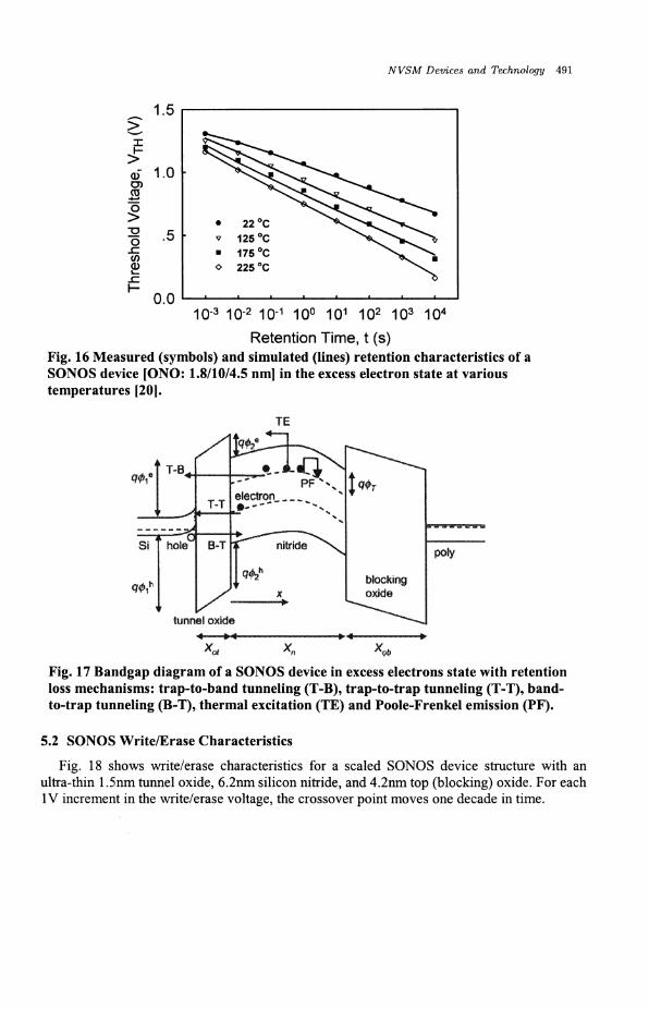
interface [18-19]. In the early stages of charge loss the trapped charge nearest the tunnel oxide-silicon nitride interface back-tunnels to the semiconductor, while in the later stages thermal emission followed by back-tunneling dominates the loss process in SONOS devices. SONOS devices with a 1.8 nm tunnel oxide have an extrapolated memory window of 0.5V to 10 years at 125C, which is sufficient to meet the needs of both military as well as commercial applications. NROM™ devices typically operate with a thicker bottom or tunnel oxide of 5 nm and suffer less stored charge loss due to reduced back-tunneling, although higher erase voltages than SONOS devices are generally required. We have developed a retention model to include both back-tunneling as well as thermal emission from traps in the silicon nitride. Fig. 16 illustrates the model to characterize the threshold voltage decay as a function of temperature [20].
NVSM Devices and Technology 491
10-3 io-210-1 io° io1 102 103 104
Retention Time, t (s) Fig. 16 Measured (symbols) and simulated (lines) retention characteristics of a SONOS device [ONO: 1.8/10/4.5 nm] in the excess electron state at various temperatures [20].
tunnel oxide
Fig. 17 Bandgap diagram of a SONOS device in excess electrons state with retention loss mechanisms: trap-to-band tunneling (T-B), trap-to-trap tunneling (T-T), band-to-trap tunneling (B-T), thermal excitation (TE) and Poole-Frenkel emission (PF).
5.2 SONOS Write/Erase Characteristics
Fig. 18 shows write/erase characteristics for a scaled SONOS device structure with an ultra-thin 1.5nm tunnel oxide, 6.2nm silicon nitride, and 4.2nm top (blocking) oxide. For each IV increment in the write/erase voltage, the crossover point moves one decade in time.

492 M. H. White et al.
Single Transistor in NSONOS Array Wafer 63570-2 Right Die 80A Oxynitride
1.0E-07 1.0E-06 1.0E-0S 1.0E-04 1.0E-03 1.0E-02
Programming Time [s] 1.0E-01 1.0E+00
Fig. 18 Program (Write)/Erase Electrical Characteristics for a Scaled SONOS NVSM Device [Preconditioned with +7V (2.5 msec) write and -7V (7.5 msec) erase]
The initial tunnel oxide electric field S0T (0+) with programming voltage VP controls the injection current from the semiconductor through the tunnel oxide into the silicon nitride and is given by the relationship [21]
^esiqNB^F
Cm ,(0+) =
VP-< -VT0(VT) + Urn Po
• + 2(/)F+-
'eff (1)
*>eff
where Xeff is the effective gate dielectric thickness, Ceff the effective gate capacitance, NB the substrate doping density, <|)F the Fermi potential, <|>s the surface potential, and VTO(0~ ) the initial threshold voltage. The factor, which contains the drain current, IDS, and gain parameter p0 f |^o(W/L)Cox, accounts for the SONOS device geometry since the threshold voltage is measured at a fixed current level [i.e. see Fig. 14{b}]. In a typical SONOS device (see Fig. 18) with a Xcff = 10 nm and a +7V write 1-1 erase operation, the initial electric field across the tunnel oxide is 9.5 MV/cm for the write operation [VT0 (0") = -2.5 V] and -7.5 MV/cm for the erase operation [VT0 (0") = +0.5 V]. The electric field in the tunnel oxide of a SONOS device determines the physical mode of carrier injection as shown in Fig. 19. For electric fields described in this example, carrier injection
Fowler Nordlteim Tunneling
IN l i f t \
Si : ^ : X
Direct Band-to Band Tunneling
occurs when
Modified Fowier Nordheiin Tunneling
occurs when
Trap-assisted Tunneling
V* '
i :
** i StsK j
^H >W>rt %!*<%x/eH>X1( %I
occurs when < • * - * * - • * - • $ %i*<%x/%>%
Fig. 19 Tunneling Mechanisms in a SONOS device for various oxide electric fields

NVSM Devices and Technology 493
occurs with Modified Fowler Nordheim (MFN) tunneling since MFN tunneling takes place for fields less than 12 MV/cm in the tunnel oxide. In this example, with a tunnel oxide of 1.5 nm, electron transport takes place with trap-assisted-tunneling (TAT) when the electric field drops below 7 MV/cm. This occurs during program operation since the storage of charge in the silicon nitride acts to reduce the electric field, SOT, in the tunnel oxide (see the above expression as the threshold voltage reduces and changes sign while the pulse remains on the gate electrode of the device). Thus, during a program and erase mechanism, the transport mechanism may change from Direct Tunneling to Modified Fowler Tunneling to Trap-Assisted-Tunneling depending upon the magnitude of the applied voltage and the initial charge stored in the silicon nitride.
5.3 SONOS Endurance Characteristics
The ability of a NVSM to retain memory after repeated write/erase cycles is called endurance. The endurance is influenced by stress caused by the electric field applied to the ONO dielectric and the magnitude of the injected carriers associated with the repeated recombination of injected carriers with traps at the Si-Si02 interface and traps within the silicon nitride dielectric. In a SONOS device the application of repeated write/erase cycles creates acceptor-like interface traps at the Si-Si02 interface, which is reflected in a small threshold shift in the positive direction and a loss of memory retention. Fig. 20 illustrates the influence of cycling on a SONOS device, where the erase state memory is primarily affected by the repeated write/erase cycling. The formation of an interface trap through the impact with a free carrier is associated with the breaking of Si - H or Si - OH bonds at the Si-Si02. In the retention mode the gate of the SONOS device is grounded and in the erase state the device is in the ON condition with an inversion layer. Thus, electrons are available in the conduction band and in the interface traps for trap-to-trap (T-T) tunneling as shown in Fig. 17. If the positive state of the trap is in-line with an interface trap, then enhanced discharge can occur with an increase in the density of interface traps. If interface traps are associated with memory retention, then we should see a correlation between SONOS devices treated conventionally with a post metal anneal (PMA), which involves hydrogen (H2) and a device subjected to deuterium (D2). Figs. 21-23 show two SONOS devices - one treated with hydrogen and the other with deuterium with clear benefits for the latter in terms of decreased interface trap creation with extended cycling [22].

494 M. H. White et al
NSONOSiliO Array Wafer 63570-2, SOAOxynitri
TV / 2.5 msec, -TV / T.5 ms10 V*
_
-0 cycles
- 0 cycles
-1E4 cycles
1E4 cycles
1E5 cycles
1E5 cycles
LJi '***& &M*-
zz
~-<,
m
$£*•
teftfi
-_
wi Tii
—
ne|.
-•-i ~"^-"
-• -_-;;
1.E-C4 1JE^3 1.E-82 1.M1 1.E*00 1.E+01 t.E*G2 1.E*63 1,E*84 1.E+S5 1.E-HK 1J»*07 1.E*88 1.E+88 1.E-H9
Fig. 20 SONOS endurance subjected to write/erase cycling.
S5C - P V l m s + l O V l m s
« Precycte
- A - 10fiCyctes
107 Cycles
10 years
« w 0
1 -e— 10%%/N2
[ -9V 1ms +llhr Inn Cycles
f 8*-=̂ — _ • ' "̂ #-
/ /
/ /
/ / --0'
10 10 10 10 10'
Erase/Write Cycles
Fig. 21 Charge Pumping Si-Si02
interface traps in SONOS devices subjected to write/erase cycling. The devices are treated with H2 and D2 [22].
i S C -9V lms+10V lass
•--#.— Pretycle
—is— 10fiCjcfcs
—«— io Cycles
Retention Time [s] 10 10 10 10 10 10
Retention Time [$]
Fig. 22 Endurance of H-treated SONOS under write/erase cycling [22].
Fig. 23 Endurance of D-treated SONOS under write/erase cycling [22].
6.0 Simulation of NROM™ NVSM Devices
NROM™ devices based on polysilicon-oxide-nitride-oxide-silicon (SONOS) structures employ localize charge trapping, which is appealing for nonvolatile memories beyond the floating gate technology, due to the compatibility of NROM™ technology with standard CMOS technology, low-voltage programming, immunity to erratic charge loss and capability of 2-bit/transistor storage with the possibility of multi-level charge (MLC) storage in the future. The operation of these structures has been described in Fig. 6-8; however, the use of channel-hot-electron (CHE) injection and hot-hole injection (HHI) in NROM™ technology [1] raises a concern on endurance. In addition, the mismatch between the electron and hole trapping locations can lead to a buildup of residue charge. Also, low charge-injection efficiency of the CHE process leads to increased power consumption. Finally, there is

NVSM Devices and Technology 495
concern over the spreading of injected charge as a limit to ultimate packing density for 2-bit and possible MLC storage. We have carried out simulations on NROM™ device operation with and without so-called pocket implants (see Fig. 24), which are used to locally increase the electric field near the drain and source regions, thereby, improving the charge-injection efficiency. The simulations are performed with Silvaco's ATLAS program. We can see the presence of a pocket implant narrows the carrier injection region from 40 nm to 10 nm to
(a) Pocket Implant (b) No Pocket Implant
Fig. 24 Simulations of a NROM™ NVSM device with and without Pocket Implants
We have developed a method to simulate the stored charge in a NROM™ NVSM device in order to study the influence of the localized surface potential on the subthreshold IDS - VGs characteristics of the device and the electron transport in the inversion layer. This method permits the strategic placement of an equivalent charge to carry out simulations of surface potential, such as shown in Fig. 25. The use of a 'reverse' read provides an increase in the surface potential (barrier height) to electrons, thereby, enhancing the effect of the localized stored charge on the threshold voltage. If the normal method of readout is employed, where the direction of read is the same as the direction of programming, then more charge or equivalently more programming time is needed to achieve the same write threshold voltage as determined with a reverse read condition. The difference between the normal and reverse reads translates into several orders of magnitude in programming speed. In the normal read condition the full electric field along the channel appears across the narrow charge storage region where the charge is stored, which effectively lowers the barrier height, while in the case of the reverse read condition a reduced field appears across the charge storage region. The ability to place small amounts of stored charge at specified locations in the NROM™ device affords simulations on the I-V characteristics, such as the subthreshold IDS - VGS
characteristics, where the influence of the charge spread and associated barrier height can be observed and correlated with experimental device structures.

496 M. H. White et al.
9 0.3V 1V
mr^ Hi 9 0-BV 9 0.8V
(a) Surface Potential (no charge) with normal read
(b) Surface Potential (charge) with normal read (A$s = 0.2V)
(c) Surface Potential (charge) with reverse read (A<|>s = 0.6V)
Fig. 25 Effect of normal and reverse read conditions, for fixed stored charge in the silicon nitride, on the surface potential (barrier) of an NROM™ NVSM device.
SJE-03
2.0E-03 A
Vds|V)
T T M Fig. 26IDS - VDS characteristics for NROM im device [ONO thickness 3.8/6.0/4.5 nm and CHE for VDS > 3V]
Fig. 26 shows the IDS - VDS
electrical characteristics for an experimental NROM™ device structure with an ONO of 3.8/6.0/4.5 nm for the bottom oxide, silicon nitride, and top oxide, respectively. This type of measurement is instructive because it indicates the effect of drain voltage on the programming of the device and the need to maintain the drain voltage below, in this example, 3V in order to minimize the effects of read disturb. As
mentioned previously, the device employs channel hot electron injection (CHE) at the source and drain junctions to store small amounts of charge locally in the silicon nitride. In Fig. 26 a

NVSM Devices and Technology 497
positive voltage is applied to the gate electrode, while a positive voltage is swept across the drain junction. All of the other terminals are grounded. The drain current drops when CHE occurs. The tunnel oxide for NROM™ devices is selected to inhibit back - tunneling and improve charge storage during retention as well as during the write and erase operations. The NROM™ device is in some sense a hybrid between the floating gate and SONOS devices, since CHE is used in programming (similar to the Flash™ floating gate structure) with the advantages of long-term retention, fast programming and source sharing in the memory layout for packing density, while enjoying the benefits of the SONOS technology for low program/erase voltages, immunity to single-defect discharge and over-erase, combined with a simplified process sequence for standard CMOS compatibility. The read voltage is determined by the memory cell requirements to supply sufficient read current, which sets the lower limit, while too high a voltage will induce barrier lowering, which decreases the programming window.
7.0 Novel SONOS NVSM Devices
A novel SONOS device has been created [23] with an ultra-thin 1.4 nm silicon nitride layer surrounded by 3.0 nm oxide layers for the bottom and top oxides. Fig. 27(a) illustrates the program/erase window and retention characteristics of the device, which uses HHI for write and Direct Tunneling (DT) from the gate electrode for the erase operation. With NROM™ programming the device had a 3.5V initial window and a 0.8V extrapolated memory window at 10 years. A cross-sectional TEM photo of the ONO gate stack is shown in Fig. 27(b).
> 1 m m m
>
m P
JO -2
HHI wrcie 1 IT»S
• OT erase m res Memory window 1 S> Vj
10 years
Hi
XV,
* v*»\*'
(•)
10*2 101 10° 10' 102 103 1G4 105 106 107 10s 10s
Retention Time (s) (b) TEM of ONO gate stack
Fig. 27 Novel SONOS device: HHI for write and DT from gate for erase operation [23]
An approach to lower the program and erase voltages and improve, at the same time, the memory window and retention in SONOS devices, is to employ a high dielectric constant (so-called high-K) film for the storage and blocking (top) insulators of the gate stack. We have conducted experiments with atomic-layer-deposited (ALD) A1203 for the blocking insulator in a SANOS device, where 'A' signifies aluminum oxide for the blocking insulator [24]. Fig. 28 shows C-V results obtained on an O/N/A film of 2.0/5.0/8.0 nm for an effective oxide thickness of 8.5 nm. We see low-voltage programming can be obtained with ± 5V for a flatband voltage shift, AVFB = 2.09V, which is obtained with an ALD blocking aluminum oxide insulator of 8.0 nm. A blocking insulator of ALD A1203 gives a 2.3V reduction in

498 M. H. White et al.
programming voltage for a lOMV/cm tunnel oxide electric field. Although the barrier height is reduced for electron injection from the gate electrode, the increase in blocking insulator thickness prevents electron injection from the N+ gate electrode during the erase operation, thereby, increasing significantly the program window. Fig. 29 illustrates the energy band structures for SONOS and SANOS devices. The relative dielectric constants are KQ = 3.9 and KA = 9.0, which allows a tradeoff between thickness selections in these devices.
1 2.5E-03
re ® 2.0E-03
< Q 1.5E-03
1.0E-03
* ^ *v
Fresh Device
~+5¥ for 2.5ms
--5V for 2.5ms
AVFR=2.09 V
-2.5 -2.0 -1.5 -1.0 -0.5 0.0
Voltage (¥)
Fig. 28 C-V program/erase characteristics for a SANOS NVSM device with an O/N/A film of 2.0/5.0/8.0 nm. ALD aluminum oxide is used for the blocking insulator [24].
Si Si02 Si3N4 Si02 poly-Si Si Si02 Si3N4 A12CS poljr»Si
3.1
1 1.12 eV
4.75
T 2.8
A.
4.8
(a) SONOS Device Structure (b) SANOS Device Structure
Fig. 29 The energy band structures for SONOS and SANOS Devices [24]

NVSM Devices and Technology 499
8.0 Conclusions
This paper provides an overview of recent developments in SONOS and NROM™ nonvolatile semiconductor memory (NVSM) devices. These devices offer unique possibilities for low-power, low-voltage high-density NVSM compatible with standard, single-polysilicon CMOS technology. The SONOS device operates with Modified Fowler Nordheim (MFN) tunneling in both program (write) and erase modes. This NVSM device provides very low power cell and can be used in either a moderate density NOR architecture with isolated source lines or a high-density, multi-byte, NAND architecture. A unique feature of SONOS NVSMs lies in their radiation hardness for military and space applications.
The NROM™ device, which operates with CHE in the program (write) mode and HHI in the erase mode, offers two-bit, high-density, storage with spatial isolation and the future possibility of multi-level-charge (MLC) storage in each spatial bit. If only single-bit storage is contemplated with MLC, then this device can operate with MFN in the erase mode, where the entire channel is erased. The sharing of source lines provides nearly a 2F2 cell area in layout, where F is the feature size of the technology. Scaled SONOS and NROM™ NVSM devices are aided with 2D simulations. In particular, 'pocket' implants may be optimized through simulations to localize the hot electron and hole injection to less than 40 nm to limit charge spreading into the channel. Future research is needed to determine if lateral charge spreading will occur with temperature in these devices.
New solutions are needed to extend multi-bit and multi-level charge storage to the sub 100 nm nodes of the ITRS, although NVSMs lag DRAMs and microprocessor/logic development due to the size of the erase/write voltages. Thus, we need to investigate means to decrease the program and erase voltages in NVSMs. The introduction of a high-K insulator, such as A1203, for the blocking or 'cap' dielectric will permit a lowering of the erase/write voltages and increase the program window since charge transfer is inhibited to and from the gate electrode. Through the use of high-K insulators in the gate stack we should be able to achieve ± 5V program/erase voltages. Finally, we need to decrease the temperature sensitivity and increase endurance to erase/write cycling through the use of innovative processes, such as with the use of deuterium anneals.
9.0 Acknowledgements
The authors wish to express appreciation to Dr. Rajinder P. Khosla and Dr. Usha Varsney of the Electrical and Communication Systems (ECS) Division in the Engineering Directorate of the National Science Foundation for their continued support of the scientific and engineering research into charge transport and storage in advanced nanoscaled SONOS devices. In particular, we express our gratitude to Dr. Varshney who helped to organize and provide partial support for the Workshop on Future Electronics (WOFE) 2004. A shortened form of this paper was an invited presentation to the attendees of the Workshop. Finally, we would like to express our appreciation to the engineers and management of the Northrop Grumman Corporation in Baltimore, MD for their continued support of SONOS technology.

500 M. H. White et al.
10.0 References
1.0 http://www.itrs.net/Common/2004Update/2004 03 PIDS.pdf This website provides and updated International Roadmap for Semiconductors (ITRS) Tables 50(a) and 50(b) describe projections for Nonvolatile Semiconductor Memory Devices and Circuits.
2.0 Nonvolatile Semiconductor Memory Technology. IEEE Press, Ed. W. D. Brown and J. E. Brewer, Chpt. 5, SONOS Nonvolatile Semiconductor Memories, F. R. Libsch and M. H. White, 309-357: 1998.
3.0 M. H. White, D. A. Adams and J. Bu, On the Go with SONOS, IEEE Circuits Dev., j j j , 22 (2000). 4.0 Y. Kamagaki amd S. Minami, MNOS Nonvolatile Semiconductor Memory Technology: Present
and Future, IEICE Trans. Electron, E84-C. No. 6, 713- 723 (2001). 5.0 W. S. Feng, T. Y. Chan, and C. Hu, MOSFET drain breakdown voltage, IEEE Electron Device
Lett., 6, 449 (1986) 6.0 E. Lusky, Y. Shacham-Diamand, I. Bloom, and B. Eitan, Characterization of Channel Hot Electron
Injection by the Subthreshold Slope of NROM™ Device, IEEE Elec. Dev. Lett., 22, 556-558 (2001)
7.0 J. Bu and M. H. White, Design Considerations in Scaled SONOS NVSM, Solid-State Electronics, 45,113-120(2001).
8.0 C. C. Chao and M. H. White, Characterization of Charge Transport and Trapping in Scaled SONOS/MONOS memory Devices, Solid-State Electronics, 30, 307 (1987).
9.0 F. R. Libsch and M. H. White, Charge transport and storage of low programming voltage SONOS/MONOS memory devices, Solid-Sate Electronics, 33, 105-126 (1990)
10.0 A. Roy and M. H. White, A New Approach to Study Electron and Hole Separation at the Semiconductor-Insulator Interface, IEEE Trans. Elect. Dev., 37, 1504 (1990) and Anirban Roy and Marvin H. White, "Electron and Hole Charge Separation with a Dual Channel Transistor", IEEE Transactions on Electron Devices, 36, 11, November 1989.
11.0 R. E. Paulsen, M. L. French and M. H. White, Observation of near-interface oxide traps with the charge pumping technique, IEEE Electron Dev. Lett., L3, 627 (1992)
12.0 R. E. Paulsen and M. H. White, Theory and application of charge pumping for the characterization of Si-Si02 interface and near-interface oxide traps, IEEE Trans. Electron Devices. 41, 1213 (1994).
13.0 D. Bauza and G. Ghibaudo, Respective contributions of the fast and slow traps to charge pumping measurements, Microelectronics Engineering (Elsevier), 28, 325 (1995)
14.0 J. Bu and M. H. White, Electrical Characterization of the ONO Triple dielectric in SONOS nonvolatile memory devices, Solid-State Electronics, 45, 47 (2001).
15.0 T. J. Krutsick, M. H. White, H-S Wong and R. V. Booth, An Improved Method of MOSFET Modeling and Parameter Extraction, IEEE Trans, on Electron Devices, 34, August 1987.
16.0 H-S Wong, M. H. White; T. J. Krutsick, and R. V. Booth, Modeling of Transconductance Degradation and Extraction of Threshold Voltage in Thin Oxide MOSFET's, Solid-State Electronics, 30, August 1987.
17.0 Marvin H. White, Yijie (Sandy) Zhao, Yu (Richard) Wang, Stephen J. Wrazien, Joel D. Krayer, Dennis A. Adams and James R. Murray, Scaled SONOS NVSM Devices for Space and Military Applications, NASA/JPL Non-Volatile Memory Technology Symposium (NVMTS), Pasadena, CA November 11-13,2003
18.0 Y Hu and M. H. White, Charge retention in scaled SONOS nonvolatile semiconductor memory devices - modeling and characterization, Solid-State Electronics, 36, '401 (1993).
19.0 Y. Yang and M. H. White, Charge retention of scaled SONOS nonvolatile memory devices at elevated temperature, Solid-State Electronics, 44, 949-58 (2000)

NVSM Devices and Technology 501
20.0 Yu Wang and Marvin H. White, An analytical retention model for SONOS nonvolatile memory devices in the excess electron state, Solid-State Electronics, 49, 97 (2005).
21.0 M. L. French and M. H. White, Scaling of multidielectric nonvolatile SONOS Memory Structures, Solid-State Electronics, 37, 1913 (1994).
22.0 J. Bu and M. H. White, Effects of two-step high temperature deuterium anneals on SONOS nonvolatile memory devices, IEEE Electron Dev. Lett., 22,17 (2001)
23.0 Y, Wang, Y. Zhao, B. M. Khan, C. L. Doherty, J. D. Krayer and M. H. White, A novel SONOS nonvolatile flash memory device using substrate hot-hole injection for write and gate tunneling for erase, Solid-State Electronics, 48, 2031 (2004).
24.0 Marvin H. White, Dennis A. Adams, James R. Murray, Stephen Wrazien, Yijie (Sandy) Zhao, Yu (Richard) Wang, Bilal Khan, Wayne Miller and Rajiv Mehrotra, Characterization of Scaled SONOS EEPROM Memory Devices for Space and Military Systems, NASA/JPL Non Volatile Memory Technology Symposium (NVMTS), Orlando, Fla November 2004.