advances in manufacturing of molded tips for scanning ... · journal of microelectromechanical...
TRANSCRIPT
JOURNAL OF MICROELECTROMECHANICAL SYSTEMS, VOL. 21, NO. 2, APRIL 2012 431
Advances in Manufacturing of Molded Tips forScanning Probe Microscopy
Nicolaie Moldovan, Zhenting Dai, Hongjun Zeng, Senior Member, IEEE, John A. Carlisle, Tevis D. B. Jacobs,Vahid Vahdat, David S. Grierson, Jingjing Liu, Kevin T. Turner, and Robert W. Carpick
Abstract—A common method for producing sharp tips usedin scanning probe microscopy (SPM) and other applications in-volving nanoscale tips is to deposit thin-film materials, such asmetals, silicon nitride, or diamond-based films, into four-facetedpyramidal molds that are formed by anisotropic etching into a(100) silicon substrate. This well-established method is capableof producing tips with radii as small as a few nanometers. How-ever, the shape of the tip apex is difficult to control with thismethod, and wedge-shaped tips that are elongated in one dimen-sion are often obtained. This limitation arises due to the practicaldifficulty of having four planes intersecting at a single point.Here, a new method for producing three-sided molds for SPMtips is demonstrated through the use of etching in (311) siliconwafers. It is shown that silicon nitride and ultrananocrystallinediamond tips fabricated with this new method are wedge freeand sharp (< 10 nm radius), thereby restoring tip molding as awell-controlled manufacturing process for producing ultrasharpSPM tips. [2011-0209]
Index Terms—Atomic force microscopy (AFM), crystallo-graphic etching, molding, scanning probe microscopy (SPM),silicon, tips.
I. INTRODUCTION
T IP MOLDING is a well-known nanofabrication methodfor producing ultrasharp tips, such as those used in scan-
ning probe microscopy (SPM) [1]–[3], field emitters [4], [5],vacuum electronics [6], [7], or tunneling-based devices [8].Tip molding consists of etching a pyramid-shaped pit into a
Manuscript received July 18, 2011; revised September 7, 2011; acceptedSeptember 30, 2011. Date of publication December 2, 2011; date of currentversion April 4, 2012. This work was supported in part by the National ScienceFoundation (NSF) through the Small Business Technology Transfer Programunder Phase II and Phase IIB Grants 0638030 and 0823002 and in part bythe Nano/Bio Interface Center under NSF Nanoscale Science and EngineeringCenter Award DMR08-32802. The work of K. T. Turner was supported by theNSF Civil, Mechanical and Manufacturing Innovation (CMMI) Division underGrant 0825000. The work of R. W. Carpick was supported by the NSF CMMIDivision under Grant 0826076. Subject Editor R. R. A. Syms.
N. Moldovan, Z. Dai, H. Zeng, and J. A. Carlisle are with Ad-vanced Diamond Technologies, Inc., Romeoville, IL 60446 USA (e-mail:[email protected]; [email protected]; [email protected]; [email protected]).
T. D. B. Jacobs, V. Vahdat, and R. W. Carpick are with the University ofPennsylvania, Philadelphia, PA 19104 USA (e-mail: [email protected]).
D. S. Grierson was with the University of Wisconsin, Madison, WI 53706USA. He is now with systeMECH, LLC, Madison, WI 53703 USA.
J. Liu was with the University of Wisconsin, Madison, WI 53706 USA. Sheis now with Applied Materials, Inc., Santa Clara, CA 95054-3299 USA.
K. T. Turner was with the University of Wisconsin, Madison, WI 53706USA. He is now with the University of Pennsylvania, Philadelphia, PA 19104USA (e-mail: [email protected]).
Color versions of one or more of the figures in this paper are available onlineat http://ieeexplore.ieee.org.
Digital Object Identifier 10.1109/JMEMS.2011.2174430
sacrificial substrate (typically silicon), depositing the desiredthin-film material into the mold, processing further to defineother features in the deposited material such as a cantileverarm, and then removing the sacrificial substrate to reveal apyramid-shaped tip. The most common mold geometry is asquare (four-sided) pyramid etched into a Si (100) wafer viaanisotropic etching [9], [10] in an alkaline solution (e.g., potas-sium hydroxide (KOH), tetramethylammonium hydroxide, Eth-ylenediamine and pyrocathechol, or others). Such molds arefour-faceted pyramids, with each facet belonging to the slow-etching {111} family of planes. Indeed, we have shown thatmonolithic ultrananocrystalline diamond (UNCD) atomic forcemicroscopy (AFM) probes with integrated tips can be formedwith this method, and the tips show exceptional wear resistanceunder harsh conditions compared to molded silicon nitridetips [11].
Additionally, such pits can be sharpened by oxidation [12],which improves the aspect ratio and lowers the radius at thebottom of the pit. Square pyramids in Si (100) wafers can beproduced by patterning either perfect squares or circles intoa hard mask layer, such as SiO2, Si3N4, or certain metals,used to protect the surrounding Si. While tip radii in the few-nanometer range can be obtained [13] [shown in Fig. 1(a)], it iscommon to produce tips that are elongated in one dimensionand reach a form of a wedge [shown in Fig. 1(b)]. Thiswedge shape originates from the four facets of the pyramidalmold not meeting at a single point, whereas the size of thewedge depends on the precision of the lithography and etching.Optical lithography can control the equality of adjacent sides ofsquares or circle eccentricities only down to 20–50 nm, due tofactors such as illumination nonuniformities, mask imperfec-tions, proximity effects in the aerial image, and concentrationgradients in the developer. The sidewall roughness of the resist(∼10 nm) falls in the same range, while transfer of the resistpattern into the hard mask pattern copies or even amplifies thisroughness. Some additional variability in the feature size alsocomes from the misorientation of the Si wafer plane from theideal crystallographic (100) plane (typically ∼0.5◦) and fromproximity effects in etching (both of the hard mask and the Si)related to plasma or solution concentration gradients (such asproduced by stirring and bubbling). Thus, the wedge size onfour-faceted pyramidal molds can be controlled only to the limitof tens of nanometers.
Fig. 2 shows typical distributions (squares) of wedge sizesobtained from an optimized fabrication process for mak-ing pyramidal tip molds and shows median wedge sizes oftens of nanometers in two representative runs. If oxidation
1057-7157/$26.00 © 2011 IEEE

432 JOURNAL OF MICROELECTROMECHANICAL SYSTEMS, VOL. 21, NO. 2, APRIL 2012
Fig. 1. SEM images of tips formed from different four-faceted Si (100) molds. (a) “Perfect” UNCD tip molded into an oxidation-sharpened wedge-free V-groovein a Si (100) mold. (Inset) High-resolution image of the tip. (b) UNCD tip molded into a wedge-ended Si (100) imperfect and unsharpened V-groove. (c) UNCDtip molded into an oxidation-sharpened V-groove in Si (100), which is similar to the one in (b) before oxidation. Statistics show that, after oxidation sharpening,double tips separated by less than 25 nm cannot be seen, indicating that smaller wedges collapse into a single tip. Oxidation-sharpened tips, including each of thedouble tips, have radii consistently < 10 nm.
Fig. 2. (Green square markers) Wedge size distributions in four-faceted pyramids obtained on Si (100) by KOH etching starting from an oxide hard maskstructured into circles with optical lithography—two runs from previous study [25]. (Black triangle markers) Principal tip radii of diamond probes obtained on Si(311)—this study.
sharpening is used, wedges smaller than ∼25 nm will collapseto single-point tips. However, larger wedges generate doubletips, as shown in Fig. 1(c), rendering them unusable for mostapplications including AFM-based imaging. While the averagesize of a wedge-shaped tip is relatively small, the variancecan be significant, requiring additional quality control (QC)steps to discriminate and exclude the oversized wedge tips.Precise QC requires piece-by-piece inspection using scanningelectron microscopy (SEM), transmission electron microscopy(TEM), or AFM, which can be tedious and time consuming.Not only is such inspection impractical and cost prohibitivefor high-throughput manufacturing, but it can also result incontamination or damage of the tips during examination.
Because of these challenges, many manufacturers have mi-grated away from molding technology for SPM tip fabrication.For instance, traditional SPM probes made of monolithic Si3N4
have been gradually replaced by Si3N4-coated Si tips. However,coated tips have their own limitations. While Si tips can befabricated consistently with tip radii in the sub-10-nm range[14], [15], adding the Si3N4 layer increases the tip radius in
proportion to the thickness of the coating (10- to 20-nm range).Similar problems have been observed with metal- [16], SiC-,and diamond-coated probes [17], [18]. In some cases, theminimum film thickness is limited by the deposition process orby the electrical resistance requirements for the coated films,which can substantially increase the tip radius. This is thesituation for diamond-coated silicon tips, where tip radii areusually in the 50-nm range or larger.
Various improvements to the tip-molding approach havebeen proposed [19]–[22]. In one method [20], etch shapescan be designed to intentionally create large wedges at theend of etched pits, which, followed by oxidation sharpening,produce two separated sharpened tips, one at either end ofthe wedge. However, it is difficult to reliably place the twotips to ensure that they do not interfere with each other in thescanning process. This limits the useful height of such probesin the direction along the cantilever, losing the advantage ofthe overall height of the pyramid, which becomes irrelevant.While longer wedges can be designed to separate the two tipsbetter, elongated pyramidal molds have negative consequences

MOLDOVAN et al.: ADVANCES IN MANUFACTURING OF MOLDED TIPS FOR SCANNING PROBE MICROSCOPY 433
Fig. 3. Methods to avoid wedged tips in molding technology. (a) “Twin-tip”-elongated wedge probe from Olympus (OMCL-HA100WS, [20]—publicationpermit granted). (b) Two-side-molded one-side-etched (“Tomie”) UNCD probe(experimental work performed by the present authors).
on probe reflectivity, stiffness, and resonance frequency[Fig. 3(a)]. Another method, possibly augmenting the moldingmethod, involves using reactive-ion etching (RIE) of the tipmaterial after the mold has been filled to remove all materialahead of the wedge-shaped pit [Fig. 3(b)]. This is equivalentto cutting off the wedge-problem area and limiting the tip bythree planes, two obtained by molding and one obtained byetching. While such tips have the advantage of being placedat the very end of the supporting cantilevers, the sharpness ofthe tips is mostly limited by the imprecision of the RIE cut intothe deep tilted wedges. For such probes, the radii are typically∼35 nm, and furthermore, the aspect ratio is too low for manyapplications [19].
In the present work, a new fabrication method is demon-strated to produce ultrasharp tips via molding using three-sided pyramidal molds etched into (311)-oriented Si wafers.The method is compatible with oxidation sharpening to gener-ate high-aspect-ratio tips. The method was successfully testedusing Si3N4 and conductive UNCD [23] as structural tip ma-terials, showing the complete elimination of wedges and arobust tolerance to lithographic imperfections and alignmentimprecision with respect to the crystallographic orientation.Tip radii were consistently measured to be below 10 nm withoxidation sharpening and below 20 nm without oxidation sharp-ening (the triangles in Fig. 2), with significant narrowing of thedistribution curve in the large tip radius range.
II. CRYSTALLOGRAPHIC CONSIDERATIONS
The idea of using a custom-oriented Si wafer for wedge-free tip fabrication can be better understood by consideringoxidation-sharpened alignment marks used for molding-basedfabrication of UNCD probes on Si (100) wafers [24]. Suchalignment marks consist of four elongated wedged V-grooves,arranged to form an alignment cross. Fig. 4 shows a UNCDstructure molded and released from such a wedge structure,showing particularly sharp spikes at both ends of the wedge.Those spikes are always produced by oxidation sharpeningat the intersection of three Si {111} facets. The spike axisorientation is differently tilted with respect to the three edgesof the trihedron. Its orientation is approximately pointing inthe 〈100〉 direction, as do the spikes from perfect four-facetedpyramids. Choosing a crystallographic wafer plane tilted withrespect to the Si (100) plane in a convenient way [e.g., such asthat shown in Fig. 4(b) and (c)] may result in trihedral moldsand tips.
A more detailed analysis in Fig. 5 shows a portion of theSi crystal lattice with symmetrical face-centered cubic (fcc)unit cells such as ABCDA′B′C ′D′ and other vicinal cells.A wedge V-groove, like the ones shown in Fig. 4, can berepresented by the geometrical figure MNR′T ′V V ′.
The facets V MT ′V ′, V NR′V ′, and V MN belong to theSi {111} family. If we consider a point L on the directionV V ′ and the plane determined by the points L, M , and N ,we get the family of planes which one can choose as waferorientations such that the V-grooves formed by alkaline etchingresult in a triangular-base pyramid (i.e., the family of pyramidsV LMN , with L ∈ V V ′). There are several ways to choosethese planes, such that convenient symmetries characterize theV LMN pyramids. One convenient way is to choose the planesuch that the edges of the pyramid are equal to each other(V M = V N = V L = MN). In this case, the point L coin-cides with D′, and one can show that the plane D′MN is the (1,1, 3) plane, a member of the {311} family. In this approach, onecan demonstrate that the edges of the pyramid are equally tiltedwith respect to the wafer plane, which is another interestingsymmetry feature. Another high-symmetry choice of the waferplane would be such that the tilt of the plane V MN withrespect to the plane LNM is equal to the tilt of the edge V Lwith respect to the plane LMN . In this case, both longitudinaland transversal cross sections of the tip would be isoscelestriangles. In this case, the wafer plane (LMN) would haveirrational Miller indices (close to {11, 10, 29}), and the pointL lays between V and D′; the angle between this plane and the(311) plane would be ∼7.22◦. In general, planes with Millerindices belonging to the family {khh}, with 1 < k/h ≤ 3, orclose to them will generate triangular-base pyramids. While allthese choices are available for custom-oriented wafers, practi-cality requires the selection of planes with the lowest possibleMiller indices. Aside from the dominant orientations Si (100),Si (111), and Si (110), silicon wafers with (311) and (522)orientations are available, with Si (522) being less common thanSi (311). Thus, Si (311) is the best choice. In the case of Si(311), the mold pyramids and resultant tips will look like thosein Fig. 6. The lateral facets of the pyramid are all {111} facets,while the vertex V is at the intersection of three slow-etchingplanes, being as close to a single geometric point as the etchingperfection can provide.
III. EXPERIMENTS WITH Si (311) WAFERS FOR
TIP FABRICATION
Several process experiments were performed on Si (311)wafers in order to demonstrate the three-faceted triangular-basepyramid formation, to investigate their shape variability as afunction of lithography performance and mask design, and tostudy tip enhancement with oxidation sharpening. In addition,the molds were filled with both UNCD and low-stress siliconnitride, and the resulting tips were characterized.
In order to investigate the formation of three-faceted pyra-mids, a special test mask was designed which contained tri-angles of different sizes and orientations, as well as other teststructures that are described later. The main triangles on themask have the shape of isosceles triangles, MND′ in Fig. 6,

434 JOURNAL OF MICROELECTROMECHANICAL SYSTEMS, VOL. 21, NO. 2, APRIL 2012
Fig. 4. (a) UNCD molded into a wedge-shaped oxidation-sharpened alignment mark used on Si (100) wafers for probe fabrication, showing sharp spikes at theintersection of three Si {111} facets; (b) and (c) show successive levels of detail, with a sectioning plane marked as a possible wafer plane orientation that wouldresult in triangle-base pyramids as V-grooves.
Fig. 5. Geometrical considerations for choosing a wafer plane to generate triangular-base pyramids as V-grooves. The cube ABCDD′A′B′C′ is thesymmetrical unit cell (fcc) of Si, while the possible wafer planes discussed are the family of planes LMN , with L ∈ V V ′. The tinted plane D′QP correspondsto the crystallographic plane (1, 1, 3).
Fig. 6. Geometry of triangular-base pyramid pits that can be fabricated in Si (311) through anisotropic etching. The facets V MN , V ND′, and V MD′ are all{111} facets.
with the base angles γ ≈ 73.22◦ (tan(γ) =√
11) and the topangle (ϕ ≈ 33.55◦) calculated from crystallographic consider-ations. In order to form the desired pyramids, these triangleshave to be oriented properly with regard to the crystallographicaxes. To achieve this, the wafers were single-side polished witha primary flat on the [110] direction and a second minor flat per-
pendicular to the primary one. Since the flats are processed onthe ingot, all wafers/wafer flats were similarly oriented, avoid-ing ambiguities when flipping over the wafers. To determine theproper orientation of the masking triangle, the mask includedcontrol triangles with four positions, rotated by 90◦ from eachother. Four Si (311) wafers were oxidized to a thickness of

MOLDOVAN et al.: ADVANCES IN MANUFACTURING OF MOLDED TIPS FOR SCANNING PROBE MICROSCOPY 435
Fig. 7. Triangular-base pits etched in Si (311) and resulting molded tips. (a) Single etched pit, prior to the removal of the oxide mask, showing a clear formationof the three-faceted pyramid. (b) Single pit after the oxide hard mask was removed. Small facets form at the corners due to the rounding of the oxide. (c) UNCDtip molded in an etched pit, showing the formation of facets. (d) Test area with size variation and 90◦ rotation of some of the patterns. The upper row of trianglespointing down shows the correct orientation for generating trihedral tips. The larger triangles on the corners of the picture have equal base sizes of 11.72 μm,while the other triangles are scaled down with ratios of 11/12, 10/12, 9/12, 8/12, and 7/12, respectively. (e) Array of UNCD tips obtained from the test area shownin (d). The lower row of triangular-base pyramids is from molding in the upper triangular pits shown in (d).
350 nm; lithography and buffered oxide etching (BOE) wereperformed to pattern the oxide. The Si was subsequently etchedin 30% KOH at 80 ◦C for 10 min to form the pits. Images ofthe pits were taken via SEM. Fig. 7(a) shows a top view of apit prior to removing the masking oxide; the correct formationof the three-faceted pyramid can be recognized as agreeing withthe geometry in Fig. 6. Imperfections in the lithography resultedin a slight rounding of the corners, where small Si {111} facetswere generated. This can be better seen after the removal of theoxide [Fig. 7(b)] and in the images of a UNCD mold made insuch a pit [Fig. 7(c)]. Fig. 7(d) presents a view of a test areawith sequential rotations of 90◦, showing that only the triangleswith the sharp corner pointing in the [110] direction generatethe desired pyramids. Fig. 7(e) shows a UNCD mold of such atest pattern.
A portion of the test mask was designed to study the sensi-tivity of the molded tip shape to the masking triangle’s openingangle (Fig. 8). Triangles with top opening angle less thanthe nominal value (33.55◦) generated small facets at the basecorners [Fig. 8(b)], while triangles with larger opening anglesgenerated a facet at the top corner [Fig. 8(c)]. However, thecentral tip region at the bottom of the mold was consistent for alltriangle shapes, all possessing sharp tips and high aspect ratios.
Another portion of the test mask provided insight into thesensitivity of pit geometry with the relative tilt angle betweenthe mask triangle and crystallographic orientation (Fig. 9). Itis obvious that the triangle tilt results in the formation ofsmall spurious facets at the base of the triangles, but the tipregion remains well defined at the intersection of three Si (111)facets. The opening angle variation and the tilt variation studiesprove that the Si (311) solution for wedge-shape elimination is
extremely robust and stable with the primary variations in thelithographic process.
Two of the wafers with triangular-base pyramidal pits wereoxidation sharpened using a recipe that produces a 500-nmoxide on Si (100) facets. To investigate the pit shapes, moldedtips were created by depositing 500 nm of low-stress nitride(LSN) using low-pressure chemical vapor deposition (LPCVD)on two wafers (one sharpened and one not sharpened) and bydepositing 1 μm of UNCD on the other two (one sharpenedand one not sharpened). The LPCVD LSN film was used in theexperiment due to the high level of coating conformity to revealthe details of the Si (311) molds; however, charging effects dueto the insulating nature of the nitride were expected to hin-der the high-resolution SEM imaging. In contrast, the UNCDfilms were boron doped to low resistivity (0.05–0.08 Ω · cm)to prevent charging effects, but the tip-filling conformity wasexpected to be slightly worse than the LPCVD nitride. Mem-branes made of both films were released from the back sideof the wafers by KOH etching, and subsequent buffered HFetching (BOE 10%) removed the oxide from the oxidizedwafers. Pieces of these membranes were detached and imagedwith SEM and TEM.
Typical geometries for the unsharpened pyramids of moldedUNCD are shown in Fig. 7(c) and (e). Fig. 10 shows theresult of molding LSN into an oxidation-sharpened pyramidpit. One can see the formation of oxidation-sharpened spikes atall the trihedral joints between three Si (111) facets, includingat the spurious facets appearing at the bottom corners of thepyramid. This can be better seen on a smaller-scale structure,which allowed a simultaneous view of both spikes at the upperright edge of the main pyramid [Fig. 10(c)]. The secondary

436 JOURNAL OF MICROELECTROMECHANICAL SYSTEMS, VOL. 21, NO. 2, APRIL 2012
Fig. 8. Study of etched pit shape variation with the included angle of the triangle. (a) General view of the test area (covered with oxide). (b) Detailed view ofthe pit with the smallest angle (20◦), showing spurious facets at the base corners (oxide removed). (c) Detail of the pit with the highest angle (44◦), showing onelarger facet at the left edge and small facets at the triangle base (oxide removed).
Fig. 9. Variation of pit formation with the misalignment of the triangle axis with respect to crystallographic orientation. (a) Resulting molds for sequentialvariation of the tilt angle, from −5◦ to +5◦. (b) Triangle with minimum tilt (−5◦). (c) Triangle with 0◦ tilt. (d) Triangle with maximum tilt (+5◦).
Fig. 10. Low-stress silicon nitride tips that were molded into oxidation-sharpened pyramids. (a) General view of a pyramid. (b) Higher-magnification imageof the central spike with an estimated radius of < 10 nm (limited by SEM imaging resolution). The circle inset at the right of the tip has a radius of 10 nm.(c) Smaller-scale pyramid showing the formation of spikes at all spurious three-faceted corners.

MOLDOVAN et al.: ADVANCES IN MANUFACTURING OF MOLDED TIPS FOR SCANNING PROBE MICROSCOPY 437
Fig. 11. UNCD molded into oxidation-sharpened pyramids. (a) General low-magnification view. (b) High-magnification image of the apex of the tipshowing filling of the tip with a translucent amorphous carbon material. Thetip radius is measured to be less than 7 nm. The brighter opaque structures arediamond grain clusters.
spikes below the principal spike will not affect the imagingperformance of AFM probes made by this approach due totheir distance from the principal spike (approximately 4–5 μm,the height of the tips). Higher magnification SEM imaging todetermine the tip radii was limited on the LSN tips by chargingeffects; however, we can state that tip radii were well below20 nm and were consistent with those of images of other tipsmeasured to be < 10 nm [Fig. 10(b)]. On structures obtainedby molding conductive UNCD into sharpened pyramids, thegeneral shapes looked similar to those observed with the LSN,and tips as sharp as < 7 nm were measured (Fig. 11). As ageneral comment, filling the pits with UNCD becomes easieras the solid angle of the pit increases; therefore, Si (311) moldsare easier to fill than similar Si (100) molds.
One additional advantage of using Si (311) wafers for moldscomes from the fact that {311} facets etch much faster than(100) planes in alkaline solutions [24], such as with 30% KOHat 85 ◦C, used in this study. This reduces the wafer etchingfrom about 350 to about 215 min. A more complete study ofbulk micromachining with Si (311) wafers, including etchingrates, anisotropy diagrams with various solutions, and ways tofabricate alignment marks on such wafers, will be presentedelsewhere.
IV. FABRICATION AND TESTING AFM PROBES
WITH TIPS MOLDED IN Si (311) PITS
Once the tip fabrication process was characterized, UNCDprobes for AFM were fabricated using the Si (311) tech-nique. While several different types of probes are currentlyunder evaluation, the present work demonstrates the creationof dynamic-mode UNCD probes, molded in non-oxidation-sharpened pits. The nominal pit depth/tip height was chosen as7.1 μm, corresponding to a mask-level isosceles-triangle baseof 11.7 μm, the same as the structures shown in Fig. 7(a)–(c).The fabrication sequence is similar to the process describedpreviously for UNCD tips molded in four-sided pyramids [11].It comprised fabrication of the pyramidal molds, depositionof UNCD (3 μm thick), patterning the UNCD in the shapeof cantilevers and chip bodies by RIE [25] through a plasmaenhanced chemical vapor deposition (PECVD) SiO2 mask,chemical mechanical planarization of the PECVD SiO2 mask,anodic bonding to a prediced Pyrex 7740 wafer, dicing throughthe Pyrex 7740 wafer to complete the handling chip body for-mation, dissolution of the Si wafer from the back side (except a
Fig. 12. Dynamic-mode AFM probes made of UNCD by molding in Si (311)pits. (a) General view of a cantilever. (b) Characteristic three-faceted pyramidintegrated at the cantilever end. (c) Tip radius evaluation in the lateral directionwith the circle showing a tip radius of ∼6 nm. (d) Tip radius evaluation in thelongitudinal direction, with the inset showing a circle of radius 10 nm.
handling frame), and deposition of reflective Al coating (70 nm)on the back side of the cantilevers. Fig. 12(a) and (b) shows theSEM images of a 120-μm-long 32-μm-wide UNCD cantileverwith the characteristic tip shape. Fig. 12(c) shows a SEM imagewith an approximate measurement of the tip radius in the lateraldirection (perpendicular to the cantilever direction), resulting ina tip radius of ∼6 nm, while Fig. 12(d) shows a measurementin the longitudinal direction (along the cantilever), resulting ina tip radius of ∼19 nm. Statistics on tip radii performed on12 tips showed that these results are consistent for unsharpenedSi (311) molds, in that, when the mold was well filled, a mini-mum principal tip radius of less than 10 nm (typically < 7 nm)occurs in the lateral direction, while the maximum principal tipradius of less than 35 nm (typically < 20 nm) occurs in thelongitudinal direction.
These results were confirmed by AFM imaging of testsamples (NioProbe [26], TipCheck [27], and UNCD Aqua 25[28] surfaces). The tool for probe evaluation was a VeecoNanoScope IIIa. Example images are shown in Figs. 13–15.
The NioProbe sample (Fig. 13) consists of a surface denselypopulated with random spikes of height ∼5 nm and is suited forinvestigating the immediate end of the AFM tip via either blindreconstruction algorithms or inverse tip imaging. The samplecan be used for measuring the resolving capability of a tip downto ∼10 nm. Imaging of the NioProbe sample was performedwith the UNCD probe in tapping mode with 366.2-kHzcantilever-driving frequency, 1-Hz scanning rate, and 25-nmtip vibration amplitude, as produced by a 67.2-mVdriving amplitude of the actuating piezo crystal. The imagereveals features of ∼10 nm in lateral size, demonstrating thatthe tip radius at the immediate apex is at or below the 10-nmlevel.
The TipCheck sample exhibits spike and edge features thatare taller (in the range 100–140 nm) compared to those of

438 JOURNAL OF MICROELECTROMECHANICAL SYSTEMS, VOL. 21, NO. 2, APRIL 2012
Fig. 13. Dynamic-mode images of a NioProbe test sample acquired with a three-faceted pyramid probe. The lateral resolution of the image is ∼10 nm, asdetermined by the size of the smallest features resolved.
Fig. 14. Dynamic-mode imaging of a TipCheck test sample with the same three-faceted pyramid probe as that in Fig. 13.
the NioProbe sample and is used to characterize the tip shapebeyond its immediate apex. The observation of repeated tri-angular features (the left image in Fig. 14) confirms that thepyramid shape is preserved below 100–140 nm from the tipapex. The 3-D image (the right image in Fig. 14) revealsrepeated inverse images of the tip, with the sharpness of thespiked features demonstrating the sharpness of the tip apex.
The UNCD (Aqua 25) [28] test surface consists of facetednanocrystalline grains in the 3- to 5-nm size range that formgrain clusters, with a surface roughness of 10–20 nm (rms). Thefeatures on the UNCD surface are not as sharp as those on theNioProbe or TipCheck substrates but are more evenly distrib-uted and with a rounded nanoscale texture. Therefore, a UNCD
sample is able to provide consistent tip-shape characterizationthrough blind reconstruction algorithms. The hardness and low-wear properties of diamond also minimize contamination andchange of the substrate during scanning, and its high elasticmodulus and low surface energy minimize elastic deformationinduced by load and adhesion. All of these aspects suggestthat UNCD samples are well suited for characterizing AFMtips made of hard materials. Fig. 15 shows the topographicimage of such a surface with the tetrahedral UNCD probe.Blind tip reconstruction obtained by applying Scanning ProbeImage Processor (SPIP) software [29] to images of the UNCDsample confirms quantitatively the values of the two princi-pal tip-curvature radii as described before. Fig. 16 shows the
MOLDOVAN et al.: ADVANCES IN MANUFACTURING OF MOLDED TIPS FOR SCANNING PROBE MICROSCOPY 439
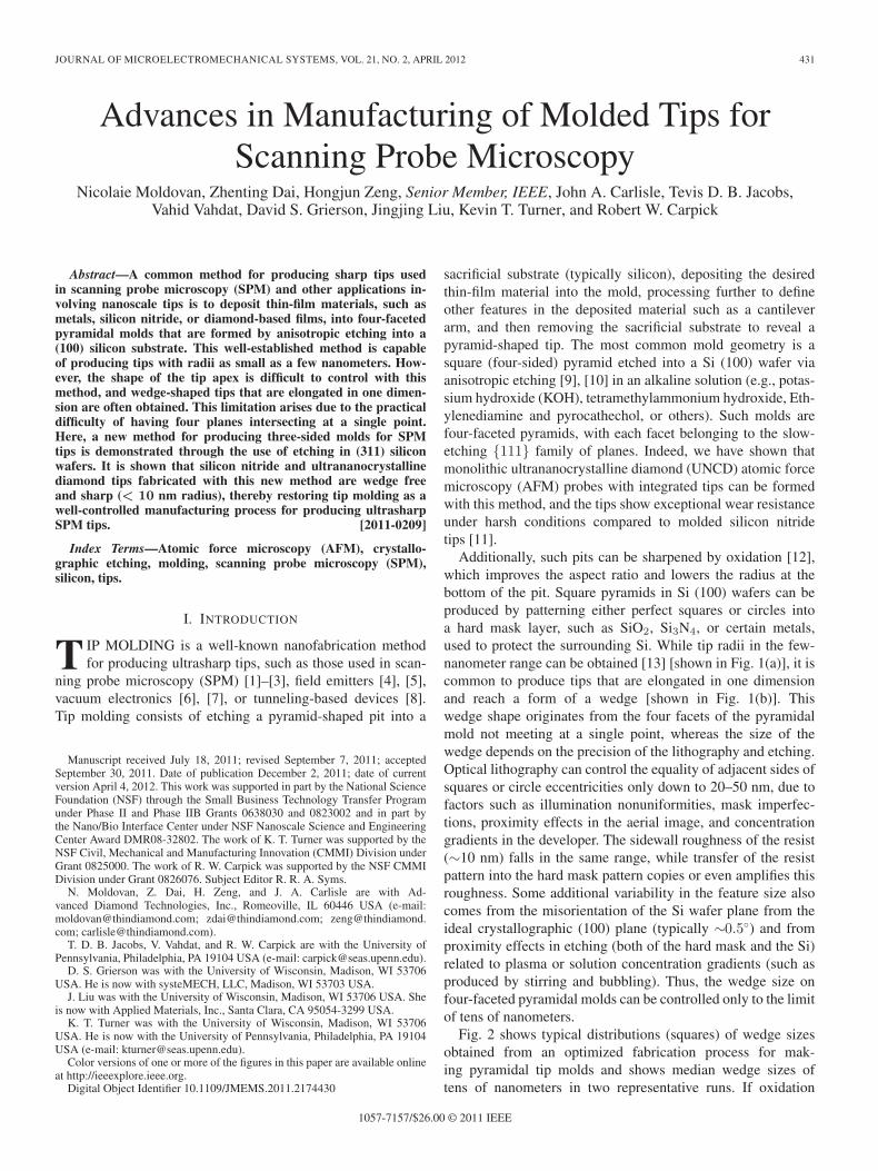
Fig. 15. Dynamic-mode imaging of a UNCD (Aqua 25) sample with the same three-faceted pyramid probe as that in Fig. 13.
Fig. 16. SPIP tip reconstruction in two orthogonal directions from an image of the UNCD sample: (a) Transverse to the cantilever and (b) along the length of thecantilever. The fitted circles to all the 27 points shown do not capture the small protrusion at the tip and give larger values for the tip radius. Fitting a circle to thefive central points captures more accurately the radius of the tip apex.
reconstructed tip profiles in the two orthogonal directions.Since both profiles are sharp close to the tip apex, fitting circlesis not the best way to characterize the tip sharpness, being scaledependent. However, to provide some upper boundary numbersfor tip radii, fitting circles was done over two size ranges: first,considering the whole 27 points of the SPIP reconstruction and,second, with only 5 points near the apex. Again, the radius inthe transversal direction is found to be smaller than the radiusin the longitudinal direction, independent of the choice for thefitting range, with a radius at the immediate apex of ∼10 nm.
A tip radius occurrence probability plot for the novel UNCDprobes molded in unsharpened Si (311) V-grooves was per-formed based on blind tip reconstruction (SPIP) from UNCDscans, with 27 points considered for the radius fittings (clearly,an upper boundary for the radii was obtained). The resultsare shown in Fig. 2 (triangle markers), overlapped with thewedge size statistics for Si (100) V-grooves from a typicalprevious set of measurements (square markers) [25]. While, inthe lower tip radius range, the improvement is incremental, theextent of the distribution curve in the larger tip radius rangeis reduced significantly. This is mostly visible in the average
tip radius improvement (∼20 nm) for the novel probes whencompared to the average wedge shape (∼62 nm) for the Si-(100)-molded probes. The near equality of the median tip radiiwith the average tip radii for the novel tips shows that the tipradius distribution (i.e., the derivative of the graphs presented)is symmetrical and close to a Gaussian distribution, which isa sign that the tip radius is now controlled by a single processfigure of merit, likely the tip-filling accuracy.
V. CONCLUSION
In the present study, a novel method has been demonstratedfor reliably manufacturing ultrasharp wedge-free nanoscale tipsusing mold pits obtained through anisotropic etching of Si(311) wafers. Contrary to commonly used molds etched in Si(100) wafers, these pits are delineated by three slow-etchingSi (111) facets and form a three-sided pyramid with an isoscelestriangle as the base. Since three planes always intersect ata point and never over a line, these molds provide a moreconsistent tip geometry that is tolerant to variations in maskshape, lithography imperfections, and angular misorientation of

440 JOURNAL OF MICROELECTROMECHANICAL SYSTEMS, VOL. 21, NO. 2, APRIL 2012
the mask relative to the crystal directions. Oxidation sharpeningof the pits produced sharp tips of silicon nitride and UNCDwhich possessed sub-10-nm tip radii and were free of wedges.Additionally, AFM probes made of UNCD based on unsharp-ened Si (311) molds were fabricated and tested, showing tipradii of < 10 nm (typically < 7 nm) in the direction parallel tothe base of the isosceles-triangle tip cross section and < 35 nm(typically < 20 nm) in the perpendicular direction.
ACKNOWLEDGMENT
The use of the Cornell Nanofabrication Facility, a memberof the National Nanotechnology Infrastructure Network, whichis supported by the National Science Foundation under GrantECS 03-35765, is acknowledged for the experimental work andprobe fabrication. Part of the work benefited from the use offacilities of the Center for Nanoscale Materials, supported bythe Office of Basic Energy Sciences, Office of Science, U.S.Department of Energy, under Contract DE-AC02-06CH11357.The use of the University of Pennsylvania Nano/Bio InterfaceCenter instrumentation is acknowledged.
REFERENCES
[1] A. Boisen, J. P. Rasmussen, O. Hansen, and S. Bouwstra, “Indirect tipfabrication for scanning probe microscopy,” Microelectron. Eng., vol. 30,no. 1–4, pp. 579–582, Jan. 1996.
[2] J. Zou, X. Wang, D. Bullen, K. Ryu, C. Liu, and C. A. Mirkin, “Amould-and-transfer technology for fabricating scanning probe microscopyprobes,” J. Micromech. Microeng., vol. 14, no. 2, pp. 204–211, Feb. 2004.
[3] K.-H. Kim, N. Moldovan, C. Ke, H. D. Espinosa, X. Xiao, J. A. Carlisle,and O. Auciello, “Novel ultrananocrystalline diamond probes for highresolution low-wear nanolithographic techniques,” Small, vol. 1, no. 8/9,pp. 866–874, Aug. 2005.
[4] W. P. Kang, J. L. Davidson, M. A. George, I. Milosavljevic, J. Wittig,and D. V. Kerns, “Characterization of the microstructure of diamondpyramidal microtip emitters,” Diamond Relat. Mater., vol. 6, no. 2–4,pp. 403–405, Mar. 1997.
[5] K. Okano, K. Hoshina, M. Iida, S. Koizumi, and T. Inuzuka, “Fabricationof a diamond field emitter array,” Appl. Phys. Lett., vol. 64, no. 20,pp. 2742–2744, May 1994.
[6] W. P. Kang, J. L. Davidson, M. Howell, B. Bhuva, D. L. Kinser,D. V. Kerns, Q. Li, and J. F. Xu, “Micropatterned polycrystalline diamondfield emitter vacuum diode arrays,” J. Vac. Sci. Technol. B, Microelectron.Nanometer Struct., vol. 14, no. 3, pp. 2068–2071, May 1996.
[7] E. Kirk, S. Tsujino, T. Vogel, K. Jefimovs, J. Gobrecht, and A. Wrulich,“Fabrication of all-metal field emitter arrays with controlled apex sizesby molding,” J. Vac. Sci. Technol. B, Microelectron. Nanometer Struct.,vol. 27, no. 4, pp. 1813–1820, Jul. 2009.
[8] Y. Hirai, Y. Kanemaki, K. Murata, and Y. Tanaka, “Novel mold fabri-cation for nano-imprint lithography to fabricate single-electron tunnelingdevices,” Jpn. J. Appl. Phys., vol. 38, no. 12B, pp. 7272–7275, Dec. 1999.
[9] P. J. Holmes, The Electrochemistry of Semiconductors. London, U.K.:Academic, 1962.
[10] R. M. Finne and D. L. Klein, “A water–amine–complexing agent systemfor etching silicon,” J. Electrochem. Soc., vol. 114, no. 9, pp. 965–970,Sep. 1967.
[11] J. Liu, D. S. Grierson, N. Moldovan, J. Notbohm, S. Li,P. Jaroenapibal, S. D. O’Connor, A. V. Sumant, N. Neelakantan,J. A. Carlisle, K. T. Turner, and R. W. Carpick, “Prevention of nanoscalewear in atomic force microscopy through the use of monolithicultrananocrystalline diamond probes,” Small, vol. 6, no. 10, pp. 1140–1149, May 2010.
[12] M. Tortonese, “Cantilevers and tips for atomic force microscopy,” IEEEEng. Med. Biol., vol. 16, no. 2, pp. 28–33, Mar./Apr. 1997.
[13] D.-B. Kao, J. P. McVittie, W. D. Nix, and K. C. Saraswat, “Two-dimensional thermal oxidation of silicon, II. Modeling stress effects inwet oxides,” IEEE Trans. Electron Devices, vol. 35, no. 1, pp. 25–37,Jan. 1988.
[14] Y. Wang and D. W. van der Weide, “Microfabrication and applicationof high-aspect-ratio silicon tips,” J. Vac. Sci. Technol. B, Microelectron.Nanometer Struct., vol. 23, no. 4, pp. 1582–1584, Jul. 2005.
[15] K. Matsuyama, “Cantilever for use in a scanning probe microscope andmethod of manufacturing the same,” U.S. Patent 5 811 017, Sep. 22, 1998.
[16] M. A. Lantz, S. J. O’Shea, and M. E. Welland, “Simultaneous force andconduction measurements in atomic force microscopy,” Phys. Rev. B,Condens. Matter, vol. 56, no. 23, pp. 15 345–15 352, Dec. 1997.
[17] K.-H. Chung and D.-E. Kim, “Wear characteristics of diamond-coatedatomic force microscope probe,” Ultramicroscopy, vol. 108, no. 1, pp. 1–10, Dec. 2007.
[18] D. Álvarez, M. Fouchier, J. Kretz, J. Hartwich, S. Schoemann, andW. Vandervorst, “Fabrication and characterization of full diamond tipsfor scanning spreading-resistance microscopy,” Microelectron. Eng.,vol. 73/74, pp. 910–915, Jun. 2004.
[19] M. Rief, H. Clansen-Schaumann, and H. E. Gaub, “Sequence depen-dent mechanics of single DNA molecules,” Nat. Struct. Biol., vol. 6,no. 4, p. 346, Apr. 1999. Biolever probes, Olympus. [Online]. Available:http://www.asylumresearch.com/Applications/LowNoise/LowNoise.pdf
[20] Olympus Probes Catalogue, Olympus Group Companies, Tokyo, Japan,p. 5, Aug. 2010.
[21] H. Shin and P. Hesketh, “Batch fabricated bifunctional AFM cantileversfor the application of SECM-AFM,” presented at the 208th Meeting Elec-trochemical Society, Los Angeles, CA, 2005, Paper MA2005-02/AA2.
[22] P. T. Lillehei, M. A. Poggi, B. J. Polk, J. A. Smith, and L. A. Bottomley,“Plastic tip arrays for force spectroscopy,” Anal. Chem., vol. 76, no. 13,pp. 3861–3863, Jul. 2004.
[23] A. R. Krauss, O. Auciello, D. M. Gruen, A. Jayatissa, A. Sumant,J. Tucek, D. C. Mancini, N. Moldovan, A. Erdemir, D. Ersoy,M. N. Gardos, H. G. Busmannf, E. M. Meyer, and M. Q. Ding, “Ultra-nanocrystalline diamond thin films for MEMS and moving mechanicalassembly device,” Diamond Relat. Mater., vol. 10, no. 11, pp. 1952–1961,Nov. 2001.
[24] H. Seidel, L. Csepregi, A. Heuberger, and H. Baumgartel, “Anisotropicetching of crystalline silicon in alkaline solutions, I. Orientation depen-dence and behavior of passivation layers,” J. Electrochem. Soc., vol. 137,no. 11, pp. 3612–3626, 1990.
[25] N. Moldovan, R. Divan, H. Zeng, and J. A. Carlisle, “Nanofabricationof sharp diamond tips by e-beam lithography and ICP-RIE,” J. Vac. Sci.Technol. B, Microelectron. Nanometer Struct., vol. 27, no. 6, pp. 3125–3131, Nov. 2009.
[26] Description of NioProbe. [Online]. Available: http://www.emsdiasum.com/microscopy/products/calibration/spm.aspx
[27] Description of TipCheck. [Online]. Available: http://www.emsdiasum.com/microscopy/products/calibration/spm.aspx
[28] Description of Aqua 25. [Online]. Available: http://www.thindiamond.com/products/uncd-wafers/uncd-aqua/
[29] Description of SPIP—Scanning Probe Image Processor. [Online].Available: www.imagemet.com
Nicolaie Moldovan received the M.Sc. and Ph.D.degrees in physics from the University of Bucharest,Bucharest, Romania.
He completed several research stages in theFraunhofer Institute for Solid State Technology,Munich, Germany, the Institut für MikrotechnikMainz, Mainz, Germany, and the Laboratoired’Analyse et d’Architecture des Systèmes, CentreNational de la Recherche Scientifique, Toulouse,France. He held the positions of Senior Researcherand Head of the Laboratory for Unconventional
Microfabrication Technologies, Institute for Microtechnology, Bucharest, forseveral years, where he ran projects in silicon and glass micromachining,atomic-scale simulation of etching, micro-optics, and LIGA. In 1998, hejoined Argonne National Laboratory, where he developed ultradeep (1 cm)LIGA technology, tilted/dynamic X-ray exposure techniques, micromachiningtechniques for new materials, such as ultrananocrystalline diamond (UNCD),and applications such as X-ray micro-optics, microfluidics, field emitters,and various microelectromechanical systems (MEMS). Since 2006, he hasbeen a MEMS Lead Scientist with Advanced Diamond Technologies, Inc.,Romeoville, IL, where he focuses on diamond atomic force microscopyprobes and applications of UNCD. He has authored or coauthored more than130 scientific papers.
Dr. Moldovan was the recipient of two R&D 100 Awards.
MOLDOVAN et al.: ADVANCES IN MANUFACTURING OF MOLDED TIPS FOR SCANNING PROBE MICROSCOPY 441
Zhenting Dai received the B.S. degree in physicsfrom Jilin University, Changchun, China, in 1996,and the M.S. and Ph.D. degrees in physics from theGeorgia Institute of Technology, Atlanta, in 2001and 2006, respectively. For his graduate work, hemicrofabricated niobium mechanically controllablebreak junctions and successfully obtained niobiumsingle-atom contacts.
From 2007 to 2010, he was a Postdoctoral Fellowwith the Nanoengineering Laboratory, University ofIllinois, Urbana. He is currently a MEMS Process
Engineer with Advanced Diamond Technologies, Inc., Romeoville, IL. He isinterested in ultrananocrystalline diamond (UNCD) atomic force microscopyprobes and UNCD MEMS devices fabrication.
Hongjun Zeng (M’05–SM’06) received the B.S.and M.S. degrees in optics from Sichuan University,Chengdu, China, in 1994 and 1997, respectively, andthe Ph.D. degree in optical engineering from the In-stitute of Optics and Electronics, Chinese Academyof Sciences, Chengdu, in 2000.
He is currently a Product Development Lead Sci-entist with Advanced Diamond Technologies, Inc.,Romeoville, IL. He is the author/coauthor of morethan 60 research papers and patents/disclosures. Hisresearch interests include advanced chemical vapor
deposition synthesis of diamond films and their applications, micro- andnanofabrication, devices, and materials.
John A. Carlisle received the B.S. degree in physicsand mathematics from Texas A&M University, Com-merce, in 1986, and the Ph.D. degree in physics fromthe University of Illinois, Urbana, in 1993.
From 1993 to 1996, he was a Postdoctoral Re-search Associate with the Lawrence Livermore Na-tional Laboratory. From 2000 to 2006, he was aPhysicist with Argonne National Laboratory. Overthe past ten years, his work has spanned thebasic–applied–commercial continuum in the area ofnanostructured carbon materials, with particular fo-
cus on the synthesis and applications of ultrananocrystalline diamond (UNCD)thin films. He is the Founder and the Chief Technology Officer of AdvancedDiamond Technologies, Inc. (ADT), Romeoville, IL. He has authored over 120publications in peer-reviewed journals.
Dr. Carlisle was the recipient of four R&D 100 Awards for UNCD-basedproducts, and ADT was named a technology pioneer in 2007 by the WorldEconomic Forum.
Tevis D. B. Jacobs received the B.Sc. degree, withmajors in mechanical engineering and materialsscience and engineering, from the University ofPennsylvania, Philadelphia, in 2003, the M.Phil.degree in computer modeling of materials fromChurchill College, University of Cambridge,Cambridge, U.K., in 2004, and the M.Sc. degreein materials science from Stanford University,Stanford, CA, in 2006. He is currently workingtoward the Ph.D. degree in materials science at theUniversity of Pennsylvania.
He worked for two years as an Engineer at Animas Corporation, a Johnson& Johnson company. His interest lies in the fundamental physics of sliding-induced wear, particularly in silicon- and carbon-based materials. Specifically,he is using atomic force microscopy and in situ transmission electron mi-croscopy to carry out experiments and using principles from chemical reactionkinetics to analyze results.
Vahid Vahdat received the B.S. degree in mechan-ical engineering from Sharif University of Tech-nology, Tehran, Iran, in 1998, and the M.S.E.degree from Villanova University, Villanova, PA,in 2004. He is currently working toward the Ph.D.degree in mechanical engineering at the University ofPennsylvania, Philadelphia.
From 2004 to 2008, he was a Research Specialistwith the Department of Radiology, University ofPennsylvania. His research interests include non-linear dynamics and nanoscale wear in amplitude-
modulation atomic force microscopy (AFM) probes and AFM/transmissionelectron microscopy characterization of the probes made out of ultrananocrys-talline diamond.
David S. Grierson received the B.S. degree inmathematics from the University of Wisconsin,Whitewater, in 2002, and the M.S. and Ph.D. degreesin engineering mechanics from the University ofWisconsin, Madison, in 2008.
From 2008 to 2011, he was a PostdoctoralResearcher with the Department of MechanicalEngineering, University of Wisconsin, Madison, in-vestigating the reliability, mechanics, and scale-upof nanomembrane-based fabrication processes andscanning-probe-based nanomanufacturing. In 2010,
he cofounded systeMECH, LLC, Madison, WI, a small business which fo-cuses on developing innovative and scalable nanomanufacturing equipment andprocesses.
Jingjing Liu received the B.S. degree in materialsscience and engineering from Southwest JiaotongUniversity, Chengdu, China, in 2002, the M.S. de-gree in applied physics from the University of NewOrleans, New Orleans, LA, in 2006, and the Ph.D.degree in materials science from the University ofWisconsin, Madison, in 2011.
She is currently a Process Engineer withApplied Materials, Inc., Santa Clara, CA. Herprevious work has focused on atomic forcemicroscopy/transmission electron microscopy char-
acterization and finite-element modeling of nanoscale wear of carbon-basedatomic force microscope tips.
Kevin T. Turner received the B.S. degree in me-chanical engineering from The Johns Hopkins Uni-versity, Baltimore, MD, in 1999, and the S.M. andPh.D. degrees in mechanical engineering from theMassachusetts Institute of Technology, Cambridge,in 2001 and 2004, respectively.
He is an Associate Professor of mechanical en-gineering and applied mechanics at the Universityof Pennsylvania, Philadelphia. Prior to joining theUniversity of Pennsylvania in August 2011, he wason the faculty of the Department of Mechanical
Engineering, University of Wisconsin, Madison, for six years. His primary re-search interests are related to manufacturing and mechanic issues in micro- andnanoscale systems. His research spans multiple topics including wafer bonding,tip-based nanomanufacturing, microfluidics, and transfer and integration ofsemiconductor nanomembranes. He is the author of more than 30 peer-reviewedjournal publications and more than 60 conference proceedings papers.

442 JOURNAL OF MICROELECTROMECHANICAL SYSTEMS, VOL. 21, NO. 2, APRIL 2012
Robert W. Carpick received the B.Sc. degree inphysics from the University of Toronto, Toronto, ON,Canada, in 1991, and the Ph.D. degree in physicsfrom the University of California, Berkeley, in 1997.
He is the Chair of the Department of Mechani-cal Engineering and Applied Mechanics, Universityof Pennsylvania, Philadelphia, where he serves asa Full Professor. He moved to the University ofPennsylvania in January 2007 after serving onthe faculty for seven years at the University ofWisconsin, Madison. He spent two years as a
Postdoctoral Appointee at Sandia National Laboratories. He works at theintersection of mechanics, materials, and physics to study nanotribology,nanomechanics, nanostructured materials, and scanning probe microscopy. Heis the author of over 80 peer-reviewed journal publications.