ae54/ac54/at54 linear ics & digital … linear ics & digital electronics june 2014 © iete 1...
TRANSCRIPT

AE54/AC54/AT54 LINEAR ICs & DIGITAL ELECTRONICS JUNE 2014
© IETE 1
Q.2 a. Classify the integration technology as per the scale of integration. Explain in brief the various steps involved in fabrication of monolithic IC.
Answer: Scales of Integration (Basic) Various steps involved in fabrication of monolithic IC
• Silicon Substrate Preparation: It involve the processing steps for growth of pure Si
crystal.
• Deposition: Films of the various materials are applied on the wafer. For this purpose mostly two kind of processes are used, physical vapor deposition (PVD) and chemical vapor deposition (CVD).
• Oxidation: In the oxidation process oxygen (dry oxidation) or H2O (wet oxidation) molecules convert silicon layers on top of the wafer to silicon dioxide.
• Photo-Lithography: The process for pattern definition by applying thin uniform layer of viscous liquid (photo-resist) on the wafer surface. The photo-resist is hardened by baking and than selectively removed by projection of light through a reticle containing mask information.
• Diffusion: A diffusion step following ion implantation is used to anneal bombardment-induced lattice defects.
• Ion Implantation: Most widely used technique to introduce dopant impurities into semiconductor. The ionized particles are accelerated through an electrical field and targeted at the semiconductor wafer.
• Etching: Selectively removing unwanted material from the surface of the wafer. The pattern of the photo-resist is transferred to the wafer by means of etching agents.
• Chemical Mechanical Polishing: A planarization technique by applying a chemical slurry with etchant agents to the wafer surface.
• Metallization Process: Metallization is the final step in the wafer processing sequence. Metallization is the process by which the components of IC’s are interconnected by aluminium conductor. This process produces a thin-film metal layer that will serve as the required conductor pattern for the interconnection of the various components on the chip.
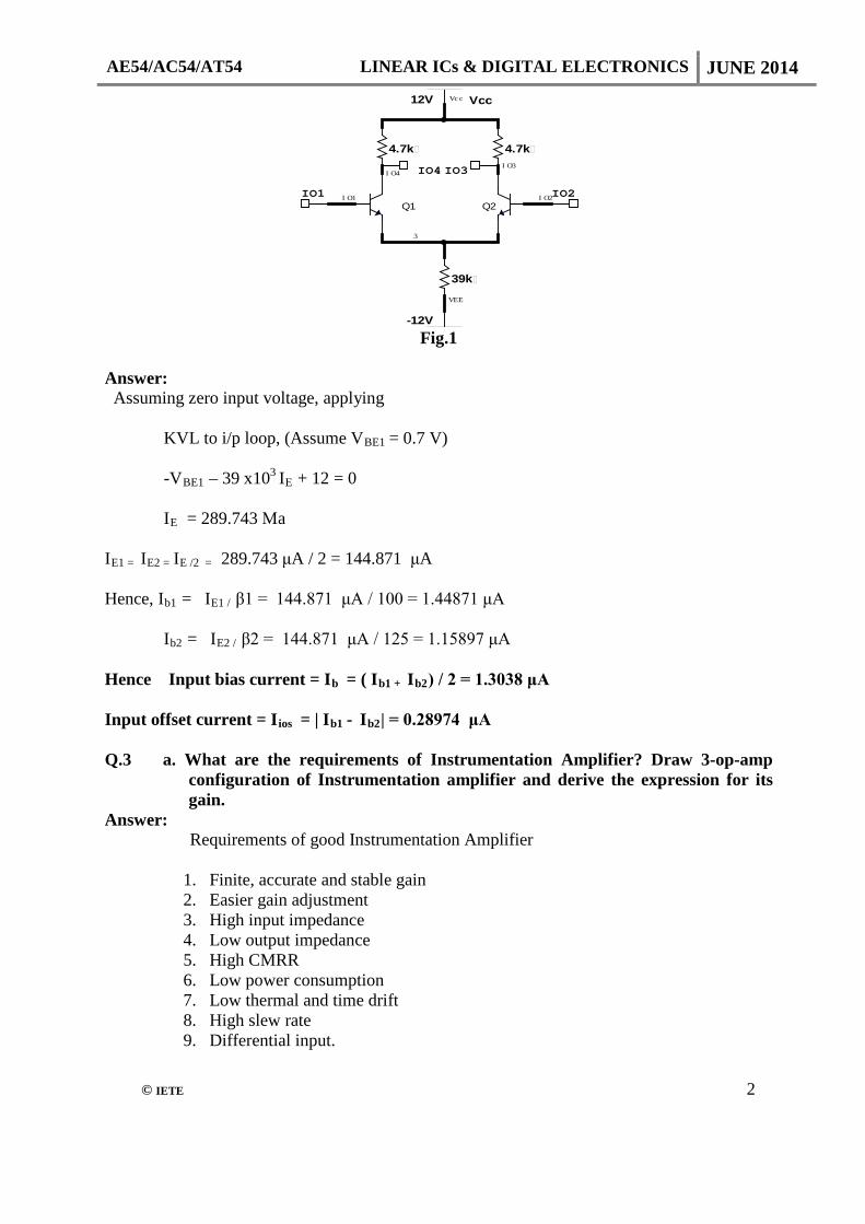
b. Calculate (i) input bias current and (ii) input offset current for the circuit
shown in Fig.1. Given that 1001 =β and 1252 =β .
Sr. No.
Integration Scale No. Of Components per chip (approx)
1 SSI (Small Scale Integration)
Up to 99
2 MSI(Medium Scale Integration) 100 - 999 3 LSI (Large Scale Integration) 1000 - 9999 4 VLSI (Very Large Scale
Integration) Above 10,000
Ultra-Large Scale Integration More than 1 million
AE54/AC54/AT54 LINEAR ICs & DIGITAL ELECTRONICS JUNE 2014
© IETE 2
Fig.1
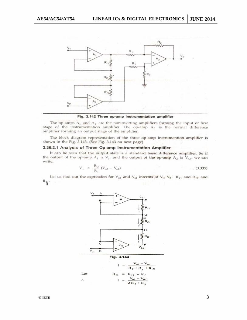
Answer: Assuming zero input voltage, applying KVL to i/p loop, (Assume VBE1 = 0.7 V) -VBE1 – 39 x103 IE + 12 = 0 IE = 289.743 Μa IE1 = IE2 = IE /2 = 289.743 μA / 2 = 144.871 μA Hence, Ib1 = IE1 / β1 = 144.871 μA / 100 = 1.44871 μA Ib2 = IE2 / β2 = 144.871 μA / 125 = 1.15897 μA Hence Input bias current = Ib = ( Ib1 + Ib2) / 2 = 1.3038 μA Input offset current = Iios = | Ib1 - Ib2| = 0.28974 μA Q.3 a. What are the requirements of Instrumentation Amplifier? Draw 3-op-amp
configuration of Instrumentation amplifier and derive the expression for its gain.
Answer: Requirements of good Instrumentation Amplifier
1. Finite, accurate and stable gain 2. Easier gain adjustment 3. High input impedance 4. Low output impedance 5. High CMRR 6. Low power consumption 7. Low thermal and time drift 8. High slew rate 9. Differential input.
Q1 Q2
4.7k 4.7k
39k
Vcc12V Vcc
IO1 IO1 IO2IO2
3
-12V
VEE
IO3IO4 IO3IO4
AE54/AC54/AT54 LINEAR ICs & DIGITAL ELECTRONICS JUNE 2014
© IETE 3

AE54/AC54/AT54 LINEAR ICs & DIGITAL ELECTRONICS JUNE 2014
© IETE 4
b. The input Vi to an op-amp is 0.04 sin 1.13 x 10⁵ t is to be amplified to the maximum extent. How much maximum gain required for an op-amp with a slew rate of 0.4 V/ μSec. Answer: The given input can be compared with Vi = Vm sin ωt and Vi = 0.04 sin 1.13 x 10⁵ t Hence, Vm (input) = 0.04 V , ω = 1.13 x 10⁵
Now, fm = S / 2π Vm and ω = 2π fm = 1.13 x 10⁵ ( Where S = Slew Rate) Hence, fm = 1.13 x 10⁵ / 2π Putting S = 0.04 V / μSec = 0.04/ 10-6 V / μSec Hence 1.13 x 10⁵ / 2π = ( 0.04/ 10-6 ) / 2π Vm Hence Vm = 3.5398 V is the magnitude of output voltage. Gain = Vm (output) / Vm(input) = 3.5398 / 0.04 = 88.5 Q.4 a. Draw and explain the ideal differentiator circuit. What are the
problems associated with it and how are they eliminated in practical differentiator?

AE54/AC54/AT54 LINEAR ICs & DIGITAL ELECTRONICS JUNE 2014
© IETE 5
Answer:

AE54/AC54/AT54 LINEAR ICs & DIGITAL ELECTRONICS JUNE 2014
© IETE 6
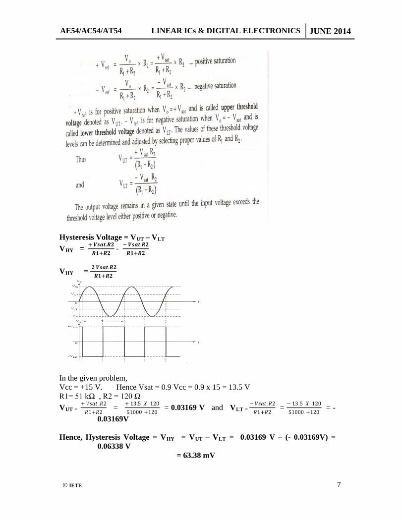
b. Explain the operation of the circuit shown in Fig.2. Also draw the
waveforms with suitable calculations by assuming CCsat V9.0V =
Answer:
AE54/AC54/AT54 LINEAR ICs & DIGITAL ELECTRONICS JUNE 2014
© IETE 7
Hysteresis Voltage = VUT – VLT VHY = + 𝑽𝑽𝑽𝑽𝑽𝑽𝑽𝑽.𝑹𝑹𝑹𝑹
𝑹𝑹𝑹𝑹+𝑹𝑹𝑹𝑹 - − 𝑽𝑽𝑽𝑽𝑽𝑽𝑽𝑽.𝑹𝑹𝑹𝑹
𝑹𝑹𝑹𝑹+𝑹𝑹𝑹𝑹
VHY = 𝑹𝑹 𝑽𝑽𝑽𝑽𝑽𝑽𝑽𝑽.𝑹𝑹𝑹𝑹
𝑹𝑹𝑹𝑹+𝑹𝑹𝑹𝑹
In the given problem, Vcc = +15 V. Hence Vsat = 0.9 Vcc = 0.9 x 15 = 13.5 V R1= 51 kΩ , R2 = 120 Ω VUT =
+ 𝑉𝑉𝑉𝑉𝑉𝑉𝑉𝑉 .𝑅𝑅2𝑅𝑅1+𝑅𝑅2
= + 13.5 𝑋𝑋 12051000 +120
= 0.03169 V and VLT = − 𝑉𝑉𝑉𝑉𝑉𝑉𝑉𝑉 .𝑅𝑅2𝑅𝑅1+𝑅𝑅2
= − 13.5 𝑋𝑋 12051000 +120
= - 0.03169V
Hence, Hysteresis Voltage = VHY = VUT – VLT = 0.03169 V – (- 0.03169V) =
0.06338 V = 63.38 mV

AE54/AC54/AT54 LINEAR ICs & DIGITAL ELECTRONICS JUNE 2014
© IETE 8
Q.5 a. State the disadvantages of Binary weighted resistor DAC and advantages of R-2R ladder network DAC. An 8 bit DAC has output voltage range from 0 to 5V, then find its resolution.
Answer: Disadvantages of Binary weighted resistor DAC-
Advantages of R- 2R ladder type DAC
- For the given DAC, n= No. Of bits = 8 , VoFS = Full scale output voltage = 5 V Resolution = VoFS / ( 2n – 1) = = 5 V / ( 28 – 1) = 0.0196 V/ LSB = 19.6 mV /
LSB b. Explain with suitable circuit diagram and waveforms Astable-multivibrator circuit operation using IC 555. Answer: Page number 318, 319 & 320 of Text Book - I.

AE54/AC54/AT54 LINEAR ICs & DIGITAL ELECTRONICS JUNE 2014
© IETE 9
Q.6 a. Compare and contrast serial and parallel data transmission technique Answer: Serial Data Transmission
1. Data is transmitted bit by bit in serial fashion 2. Data is transmitted or received in a sequence. 3. Only one conducting wire is required. 4. Thus less hardware (wires) required. 5. Cheaper. 6. It is comparative slower. 7. Data synchronization is required. 8. Useful for long distance data transfer like internet etc.
Parallel Data Transmission
1. Data is transmitted all bits at a time. 2. Data is transmitted or received in a parallel way. 3. Number of conducting wire = no. of bits. 4. Thus more hardware (wires) required. 5. Comparatively costlier. 6. It is comparative faster. 7. Data synchronization is not required as such. 8. Useful for long distance data transfer like internet etc. 9. Useful for short distance data transfer like on chip or on board data
transfer etc.
b. A digital system consists of 1024 x 8 bit memory. (i) How many address lines will it require? (ii) Specify the range of address in Hex. (iii) How many total number of bits can be stored in this memory? Answer: A digital system consists of 1024 x 8 bit memory. (i) 210 = 1024 Hence it will require 10 address lines (ii) 1024 locations X 8 bits per location = 8192 bits. (iii) 0000000000 to 1111111111 i.e. 000 H to 3FF H c. Make the following conversion (steps are necessary): (i) 100011101 to decimal (ii) (17735) 8 to Hex (iii) (ABCD )16 to binary Answer:
(i) 285 Decimal (ii) 1FDD Hex (iii) ( 1010 1011 1100 1101) binary

AE54/AC54/AT54 LINEAR ICs & DIGITAL ELECTRONICS JUNE 2014
© IETE 10
Q7 a. State and prove DeMorgan’s Theorem. Answer:
b. Implement the following expressions using NAND gates only. (i) Y = A + B+ C.D (ii) Y = Answer: (i)

AE54/AC54/AT54 LINEAR ICs & DIGITAL ELECTRONICS JUNE 2014
© IETE 11
(ii)
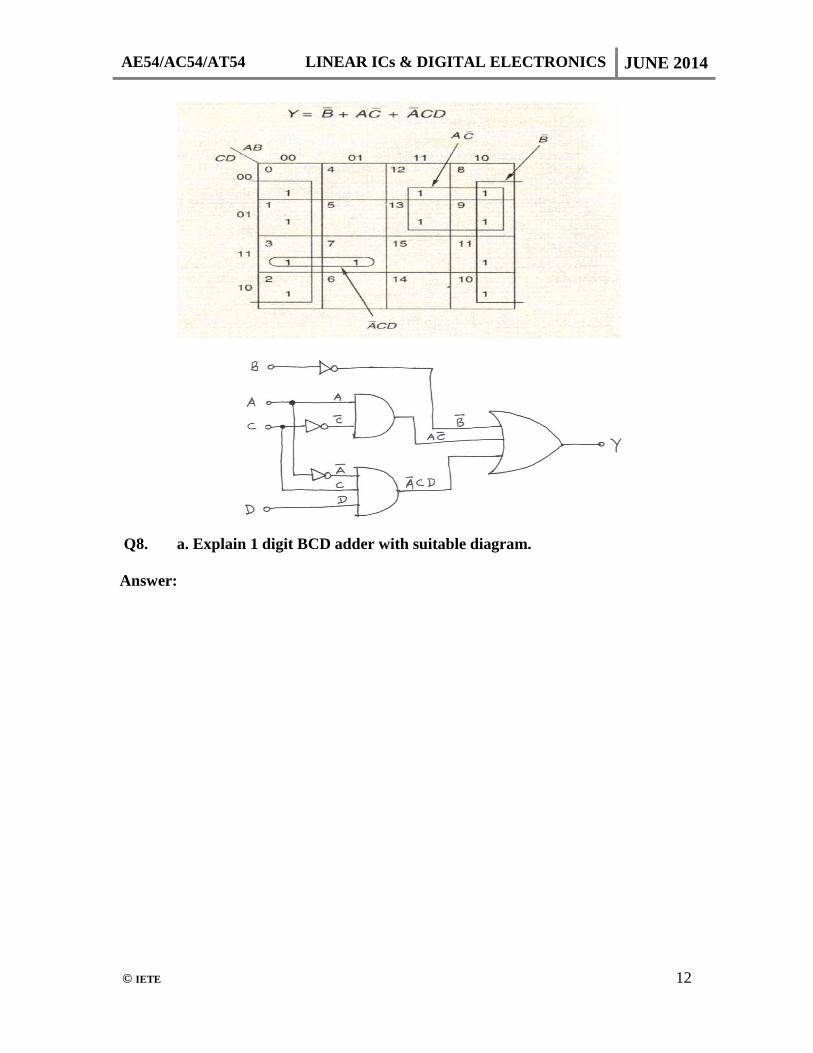
c. Simplify the expression Y = Σ m (0,1,2,3,7,8,9,10,11,12,13) using K-map and implement using basic gates. Answer:
AE54/AC54/AT54 LINEAR ICs & DIGITAL ELECTRONICS JUNE 2014
© IETE 12
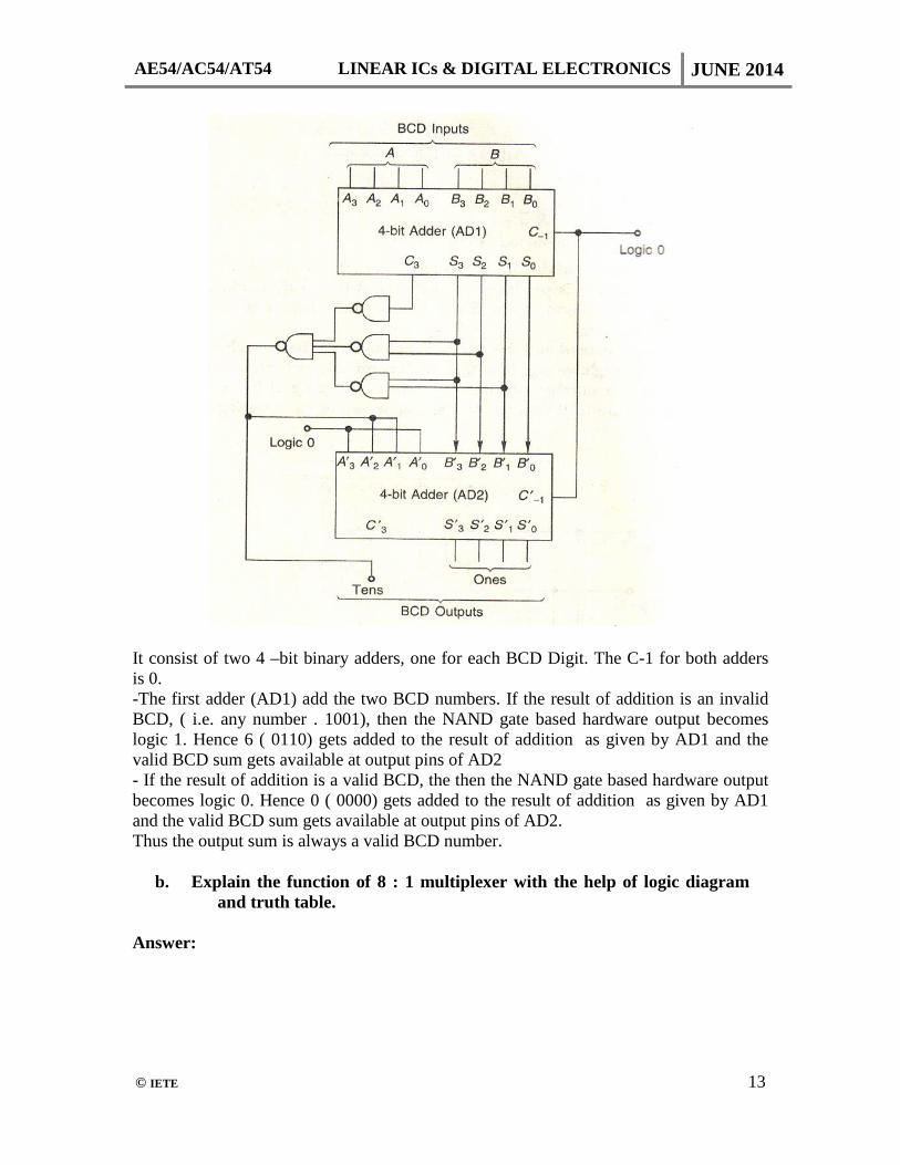
Q8. a. Explain 1 digit BCD adder with suitable diagram. Answer:
AE54/AC54/AT54 LINEAR ICs & DIGITAL ELECTRONICS JUNE 2014
© IETE 13
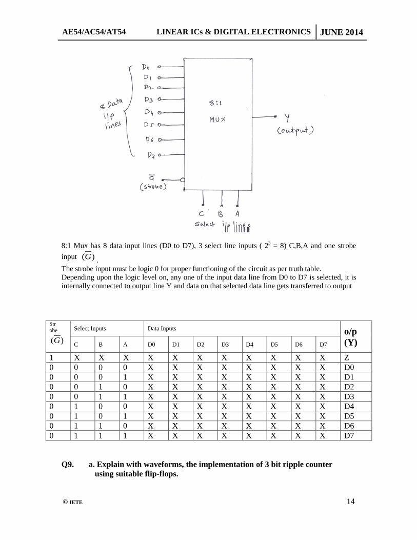
It consist of two 4 –bit binary adders, one for each BCD Digit. The C-1 for both adders is 0. -The first adder (AD1) add the two BCD numbers. If the result of addition is an invalid BCD, ( i.e. any number . 1001), then the NAND gate based hardware output becomes logic 1. Hence 6 ( 0110) gets added to the result of addition as given by AD1 and the valid BCD sum gets available at output pins of AD2 - If the result of addition is a valid BCD, the then the NAND gate based hardware output becomes logic 0. Hence 0 ( 0000) gets added to the result of addition as given by AD1 and the valid BCD sum gets available at output pins of AD2. Thus the output sum is always a valid BCD number. b. Explain the function of 8 : 1 multiplexer with the help of logic diagram
and truth table. Answer:
AE54/AC54/AT54 LINEAR ICs & DIGITAL ELECTRONICS JUNE 2014
© IETE 14
8:1 Mux has 8 data input lines (D0 to D7), 3 select line inputs ( 23 = 8) C,B,A and one strobe input )(G . The strobe input must be logic 0 for proper functioning of the circuit as per truth table. Depending upon the logic level on, any one of the input data line from D0 to D7 is selected, it is internally connected to output line Y and data on that selected data line gets transferred to output
Q9. a. Explain with waveforms, the implementation of 3 bit ripple counter using suitable flip-flops.
Strobe
)(G
Select Inputs Data Inputs o/p (Y) C B A D0 D1 D2 D3 D4 D5 D6 D7
1 X X X X X X X X X X X Z 0 0 0 0 X X X X X X X X D0 0 0 0 1 X X X X X X X X D1 0 0 1 0 X X X X X X X X D2 0 0 1 1 X X X X X X X X D3 0 1 0 0 X X X X X X X X D4 0 1 0 1 X X X X X X X X D5 0 1 1 0 X X X X X X X X D6 0 1 1 1 X X X X X X X X D7

AE54/AC54/AT54 LINEAR ICs & DIGITAL ELECTRONICS JUNE 2014
© IETE 15
Answer:
The clock pulses to be counted are given to FF0 while o/p Q0 of FFO is given as clock i/p to FF1 and so on. With T= 1, the o/p of T FF toggles with every negative edge of the clock input. The asynchronous Preset and Clear inputs are held at logic 1 for normal operation.
b. Draw the diagram of four-bit bi-directional shift register using D flip-flops and explain its operation.

AE54/AC54/AT54 LINEAR ICs & DIGITAL ELECTRONICS JUNE 2014
© IETE 16
Answer:
Text Book
(1) Linear Integrated Circuits, Revised 2nd Edition, D Roy Choudhary, Shail B. Jain, New Age International Publishers.
(2) Digital Systems - Principles & Applications, 9th Edition, Ronald J. Tocci , Neal S Widmer & Gregory L. Moss, Pearson Education, 2008.