affordable rad-hard – an impossible dream?
TRANSCRIPT

Alexander 1 22nd Annual AIAA/USUConference on Small Satellites
SSC08-XI-5
Affordable Rad-Hard – An Impossible Dream?
David R. AlexanderAir Force Research Laboratory
3550 Aberdeen Avenue, SE, Albuquerque, NM; 505-269-3895
Ken Hunt, Marc Owens, James LykeAir Force Research Laboratory
3550 Aberdeen Avenue, SE, Albuquerque, NM; 505-846-4510
ABSTRACT
Affordable electronics and radiation-hardened electronics have often been mutually exclusive terms. Recentactivities at the Air Force Research Laboratory (AFRL) and other government organizations are focused on vastlyimproving the availability and affordability of high-performance rad-hard electronics to put them into the price rangeof small satellites. The projects include the development of an advanced FPGA, structured ASICs, 16-Mbit SRAMs,and hardened versions of commercial devices such as a Texas Instrument 1394 chip set.
INTRODUCTION
Satellites, even small satellites, are expensive interms of labor hours expended, price of purchasedmodules, and launch costs. Failure of even the mosthumble piecepart (diode, transistor, etc.) can causethe mission to fail and waste all of the resourcesexpended to field it. Consequently, great care anddiscipline are required in selecting the pieceparts thatmake up the electronics packages that acquire,process, and communicate data and control thesatellite. The parts must survive launch and functionin the thermal and radiation environment of space forthe duration of the mission.
A radiation-hardened part is always the desirablechoice for a satellite application even though itsperformance (throughput, power dissipation, etc.) islower and its price is higher when compared to acommercial device. The added expense of testing acommercial microcircuit to ensure adequate radiationhardness and reliability can quickly exceed thepurchase price of a rad-hard part. Design schemessuch as TMR (triple modular redundancy) to mitigateSEE (single event effects) in commercial parts,greatly complicate the design of the hardware andsoftware, driving up cost and extending developmenttime. In cases where the commercial microcircuit issusceptible to latch-up in the space environment, on-board latch-up monitoring and recovery functionsmust be added to the system design. Such provisionsnot only increase complexity and cost, but also callinto question the reliability of parts that mayexperience latch-up even for a short time.
Despite the benefits of using radiation-hardened partsfor space system reliability and survivability, theirperformance has seriously lagged that ofcommercially-available electronics. Furthermore, thevariety of available rad-hard electronics is far lessrich than commercial offerings. Finally, the price anddelivery time for rad-hard products have often beenprohibitive for small satellites on a tight budget andshort schedule. As a result, small satellite programsare tempted to accept much greater risk than theywould like and to fly commercial parts with onlysuperficial testing.
NEW CONCEPTS IN HARDENINGMICROELECTRONICS
Improving the availability and cost of state-of-the-artradiation-hardened microcircuits is clearly a worthyobjective. Achieving this objective requires a visionof future satellite parts requirements and anappreciation of the impact on radiation hardness andhardening techniques as the semiconductor industryfollows its roadmap of shrinking feature size,advanced materials, and new processes.
The authors’ vision of the future of satellite systemsforesees continued pressure in the following areas:(1) flat or tightly constrained piecepart budgets, (2)significantly reduced development times, (3)decreased power allocations to drive down weightand reduce launch costs, (4) increased on-boardprocessing and data storage to reduce downlinkbottlenecks, and (5) standardization of interfaces. Inthe area of data processing functions, we expectsystem designers will respond to these pressures bychanging the technology mix they use to satisfy

Alexander 2 22nd Annual AIAA/USUConference on Small Satellites
processing requirements. We anticipate they willchoose a mix where roughly 50% of the functionalityis instantiated in FPGAs (field programmable gatearrays), 25% in S-ASICs (Structured ApplicationSpecific Integrated Circuits), 15% in catalog ICs, and10% in full custom ASICs. The rationale behindthose choices is to enable more of the functionality tobe instantiated in configurable microcircuits (FPGAsand S-ASICs) and hardened versions of commercialcatalog parts. In our vision, the goal is to architectthe system to restrict full-custom ASICs to those fewcritical functions requiring the most extremeperformance. This approach will enable systemdesigners to achieve the performance they need whileminimizing the high NRE costs associated with ASICdesign and mask fabrication in nano-scale (i.e., 90 nmand below) technologies. However, theseexpectations require that advanced electronictechnologies be enhanced to increase their radiationhardness while reducing non-recurring costs andassuring availability.
In the following sections, we briefly describe some ofthe programs that are in progress and provideopportunities to achieve radiation-hardened dataprocessing at an affordable cost.
Radiation-Hardened Volatile FPGA Development
The SIRF (SEU-Immune Reconfigurable FPGA)program is an effort sponsored by AFRL to develop aradiation-hardened version of the Xilinx Virtex 5commercial FPGA, specifically, the XQR5VFX130.The characteristics of the device are listed in Table 1.
Table 1: SIRF Device Characteristics
Function Size
Logic cells 131,072
6-input Look-upTables (LUT)
81,920
Distributed RAM(Kbits)
1,580
36 Kbit BRAM Blocks 301
BRAM (Kbits) 10,836
Clock ManagementTiles
6
DSP48E Slices 320
GTX Channels 20
PowerPC 440 Blocks 2
PCI Expres EndpointBlocks
3
10/100/1000 EthernetMACs
6
Select I/O 840
Rocket I/O Channels 20
The physical organization of the SIRF chip is shownin Figure 1.
Figure 1: Physical layout of the SIRF chip
Note that the functions of the SIRF Virtex 5 aresegregated into columns in the layout. This columnararchitecture facilitates the implementation ofhardening-by-design (HBD) approaches. Sizeincreases required to accommodate HBD techniquesare constrained to the vertical dimension, leaving thelateral dimension unchanged and not affecting thelateral routing resources. This permits relatively easyscaling of the size of the FPGA dimensions tomaintain required functionality even though there isan increase in the physical dimensions of the HBDcells.
The SIRF Virtex 5 is fabricated with 65nm, nano-scale technology with 12 layers of metallization. It isthe state-of-the-art commercial FPGA technology thatachieves 50% to 70% of the performance (i.e., clockfrequency, gate density, and power) of a customASIC fabricated in the same technology. However,the design costs are 70% to 80% less than the costs ofa custom ASIC; the design tools are 99% less thanASIC tools (standard Xilinx commercial tools areused for the enhanced SIRF FPGA); qualification andprocurement costs are 100% less than an ASIC (i.e.,$0); and schedule lead time is 66% to 75% less thanan ASIC. AFRL estimates that for an equivalent 1Mgate design, a standard cell ASIC developmentwould required 2 years and $10M, whereas an FPGAimplementation would require 6 months and $2M.
The primary hardening effort is being applied to limitsingle event effects (SEE). The goal of the project isto eliminate SEL (single event latch-up), reduce SEU(single event upset) in the data path circuitry to 10-2
Alexander 3 22nd Annual AIAA/USUConference on Small Satellites
errors per device day and SEU in the configurationmemory to 10-4 errors per device day. This is beingachieved by use of space and time redundancy anderror correcting techniques in the data memory, flipflops, and registers. Special electrical and layoutdesigns are used to harden the configuration memorywhile the state machines have been redesigned toeliminate SEFI (single event functional interrupts).The PowerPC 440 (PPC 440) and the Rocket I/O aremacro-cells (special purpose circuits) that are oftenused in the Virtex 5. Hardening analyses have beenconducted on those macro-cells, but the elements willnot be hardened in the initial development effort.
Two proof-of-concept test chips have been completedto date, and the first prototype of the full rad-hardVirtex 5 is scheduled to complete fabrication andtesting by the end of calendar year 2008. The finalproduct is scheduled to be available for purchase inthe first quarter of 2010.
Radiation-Hardened Structured ASIC Development
The radiation-hardened structured ASIC (S-ASIC)program is being sponsored by AFRL in an enhancedSBIR (Small Business Innovative Research) program.The program team is led by MicroelectronicsResearch and Development Corp (Micro-RDC), andincludes ViASIC, Inc., Adsantec, Sandia Technolo-gies, and Aeroflex. The program is based on astructured ASIC concept developed by ViASIC andemploys the primitive cell shown in Figure 2.
Figure 2. Structured ASIC Primitive Cell
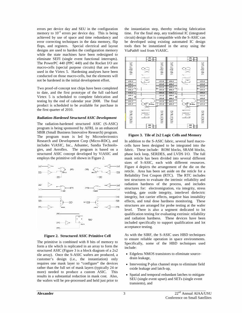
The primitive is combined with 8 bits of memory toform a tile which is replicated in an array to form thestructured ASIC (Figure 3 is a block diagram of a 2x2tile array). Once the S-ASIC wafers are produced, acustomer’s design (i.e., the instantiation) onlyrequires one mask layer to “configure” the devicesrather than the full set of mask layers (typically 24 ormore) needed to produce a custom ASIC. Thisresults in a substantial reduction in mask cost. Also,the wafers will be pre-processed and held just prior to
the instantiation step, thereby reducing fabricationtime. For the final step, any traditional IC (integratedcircuit) design that is compatible with the S-ASIC canbe developed using existing automated IC designtools then be instantiated in the array using theViaPath tool from ViASIC.
Figure 3. Tile of 2x2 Logic Cells and Memory
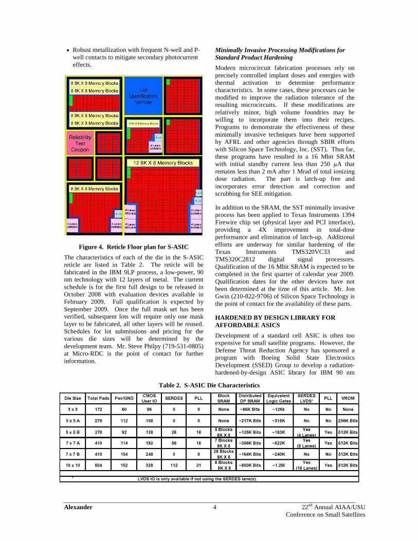
In addition to the S-ASIC fabric, several hard macro-cells have been designed to be integrated into thefabric. These include: ROM blocks, SRAM blocks,phase lock loop, SERDES, and LVDS I/O. The fullmask reticle has been divided into several differentsizes of S-ASIC, each with different resources.Figure 4 depicts the arrangement of the die on thereticle. Area has been set aside on the reticle for aReliability Test Coupon (RTC). The RTC includestest structures to evaluate the intrinsic reliability andradiation hardness of the process, and includesstructures for: electromigration, via integrity, stressvoiding, gate oxide integrity, interlevel dielectricintegrity, hot carrier effects, negative bias instabilityeffects, and total dose hardness monitoring. Thesestructures are arranged for probe testing at the waferlevel. There is also a segment dedicated to lotqualification testing for evaluating extrinsic reliabilityand radiation hardness. These devices have beenincluded specifically to support qualification and lotacceptance testing.
As with the SIRF, the S-ASIC uses HBD techniquesto ensure reliable operation in space environments.Specifically, some of the HBD techniques usedinclude:
Edgeless NMOS transistors to eliminate source-drain leakage,
Intervening P-plus channel stops to eliminate fieldoxide leakage and latch-up,
Spatial and temporal redundant latches to mitigateSEU (single event upset) and SETs (single eventtransients), and
Alexander 4 22nd Annual AIAA/USUConference on Small Satellites
Robust metallization with frequent N-well and P-well contacts to mitigate secondary photocurrenteffects.
Figure 4. Reticle Floor plan for S-ASIC
The characteristics of each of the die in the S-ASICreticle are listed in Table 2. The reticle will befabricated in the IBM 9LP process, a low-power, 90nm technology with 12 layers of metal. The currentschedule is for the first full design to be released inOctober 2008 with evaluation devices available inFebruary 2009. Full qualification is expected bySeptember 2009. Once the full mask set has beenverified, subsequent lots will require only one masklayer to be fabricated, all other layers will be reused.Schedules for lot submissions and pricing for thevarious die sizes will be determined by thedevelopment team. Mr. Steve Philpy (719-531-0805)at Micro-RDC is the point of contact for furtherinformation.
Minimally Invasive Processing Modifications forStandard Product Hardening
Modern microcircuit fabrication processes rely onprecisely controlled implant doses and energies withthermal activation to determine performancecharacteristics. In some cases, these processes can bemodified to improve the radiation tolerance of theresulting microcircuits. If these modifications arerelatively minor, high volume foundries may bewilling to incorporate them into their recipes.Programs to demonstrate the effectiveness of theseminimally invasive techniques have been supportedby AFRL and other agencies through SBIR effortswith Silicon Space Technology, Inc. (SST). Thus far,these programs have resulted in a 16 Mbit SRAMwith initial standby current less than 250 μA thatremains less than 2 mA after 1 Mrad of total ionizingdose radiation. The part is latch-up free andincorporates error detection and correction andscrubbing for SEE mitigation.
In addition to the SRAM, the SST minimally invasiveprocess has been applied to Texas Instruments 1394Firewire chip set (physical layer and PCI interface),providing a 4X improvement in total-doseperformance and elimination of latch-up. Additionalefforts are underway for similar hardening of theTexas Instruments TMS320VC33 andTMS320C2812 digital signal processors.Qualification of the 16 Mbit SRAM is expected to becompleted in the first quarter of calendar year 2009.Qualification dates for the other devices have notbeen determined at the time of this article. Mr. JonGwin (210-822-9706) of Silicon Space Technology isthe point of contact for the availability of these parts.
HARDENED BY DESIGN LIBRARY FORAFFORDABLE ASICS
Development of a standard cell ASIC is often tooexpensive for small satellite programs. However, theDefense Threat Reduction Agency has sponsored aprogram with Boeing Solid State ElectronicsDevelopment (SSED) Group to develop a radiation-hardened-by-design ASIC library for IBM 90 nm
Table 2. S-ASIC Die Characteristics
Alexander 5 22nd Annual AIAA/USUConference on Small Satellites
9SF technology[1]. By using the library for smallvolume, multi-project lots through MOSIS, customASICs can be developed for reasonable costs. Thelibrary is the property of the U.S. Government andis available for use by DoD (Department ofDefense) approved organizations through BoeingSSED. The point of contact is Dr. Warren Snapp(253-773-5722).
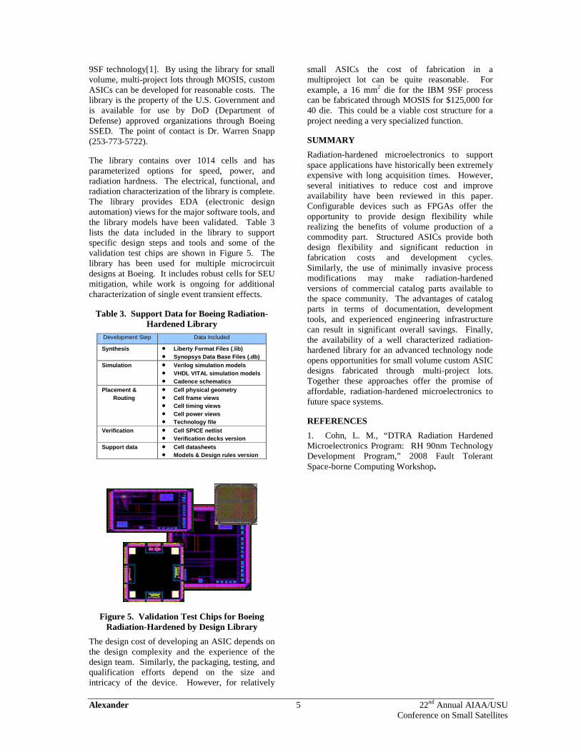
The library contains over 1014 cells and hasparameterized options for speed, power, andradiation hardness. The electrical, functional, andradiation characterization of the library is complete.The library provides EDA (electronic designautomation) views for the major software tools, andthe library models have been validated. Table 3lists the data included in the library to supportspecific design steps and tools and some of thevalidation test chips are shown in Figure 5. Thelibrary has been used for multiple microcircuitdesigns at Boeing. It includes robust cells for SEUmitigation, while work is ongoing for additionalcharacterization of single event transient effects.
Table 3. Support Data for Boeing Radiation-Hardened Library
Development Step Data Included
Synthesis Liberty Format Files (.lib)
Synopsys Data Base Files (.db)
Simulation Verilog simulation models
VHDL VITAL simulation models
Cadence schematics
Placement &
Routing
Cell physical geometry
Cell frame views
Cell timing views
Cell power views
Technology file
Verification Cell SPICE netlist
Verification decks version
Support data Cell datasheets
Models & Design rules version
Figure 5. Validation Test Chips for BoeingRadiation-Hardened by Design Library
The design cost of developing an ASIC depends onthe design complexity and the experience of thedesign team. Similarly, the packaging, testing, andqualification efforts depend on the size andintricacy of the device. However, for relatively
small ASICs the cost of fabrication in amultiproject lot can be quite reasonable. Forexample, a 16 mm2 die for the IBM 9SF processcan be fabricated through MOSIS for $125,000 for40 die. This could be a viable cost structure for aproject needing a very specialized function.
SUMMARY
Radiation-hardened microelectronics to supportspace applications have historically been extremelyexpensive with long acquisition times. However,several initiatives to reduce cost and improveavailability have been reviewed in this paper.Configurable devices such as FPGAs offer theopportunity to provide design flexibility whilerealizing the benefits of volume production of acommodity part. Structured ASICs provide bothdesign flexibility and significant reduction infabrication costs and development cycles.Similarly, the use of minimally invasive processmodifications may make radiation-hardenedversions of commercial catalog parts available tothe space community. The advantages of catalogparts in terms of documentation, developmenttools, and experienced engineering infrastructurecan result in significant overall savings. Finally,the availability of a well characterized radiation-hardened library for an advanced technology nodeopens opportunities for small volume custom ASICdesigns fabricated through multi-project lots.Together these approaches offer the promise ofaffordable, radiation-hardened microelectronics tofuture space systems.
REFERENCES
1. Cohn, L. M., “DTRA Radiation HardenedMicroelectronics Program: RH 90nm TechnologyDevelopment Program,” 2008 Fault TolerantSpace-borne Computing Workshop.