agilent technologies wireless test solutions · coding (assuming voice transmission), channel...
TRANSCRIPT

Testing and Troubleshooting Digital RF CommunicationsTransmitter Designs
I
Q
Agilent Technologies Wireless Test Solutions Application Note 1313

2
The demand for ubiquitous wireless communications is challenging the physicalconstraints placed upon current wireless communications systems. In addition,wireless customers expect wireline quality from their service providers. Serviceproviders have invested a lot in a very limited slice of the radio spectrum.Consequently, network equipment manufacturers must produce wireless systemsthat can be quickly deployed and provide bandwidth-efficient communications.
At early stages of equipment design, rigorous testing is performed to ensure system interoperability. The increasingly complex nature of digital modulation isplacing additional pressure on design teams, already faced with tight projectdeadlines. Not only must the designer test to conformance; he must also quicklyinfer possible problem causes from measurement results.
The objective of this application note is to help you understand why the different transmitter tests are important and how they identify the most commonimpairments in transmitter designs.
The application note focuses on cellular communications transmitters, althoughsome of the measurements and problems described may also apply to other digital communications systems.
This application note covers the following topics:
1. How digital communications transmitters work.2. How to test transmitters and what test equipment characteristics
are important.3. The common impairments of a transmitter and how to
troubleshoot them.
The following information is also included as reference material:
• A detailed troubleshooting procedure (Appendix A).• A table of instrument capabilities (Appendix B).• A glossary of terms.• A list of reference literature.
Introduction
3
The first two chapters in the application note, covering topics 1 and 2, are targeted at new R&D engineers who have a basic knowledge of digital commu-nications systems. The third chapter is targeted at R&D engineers with someexperience in testing digital communications transmitter designs. For basicinformation on digital modulation techniques—essential background for thisapplication note—please refer to:
Digital Modulation in Communications Systems—
An Introduction [1].
The measurements and problems described apply to most wireless communica-tions systems. Some measurements specific to common technologies or standardsare also mentioned. For more detailed information on CDMA and GSM meas-urements, please refer to:
Understanding CDMA Measurements for Base Stations
and Their Components [2]
Understanding GSM Transmitter Measurements for
Base Transceiver Stations and Mobile Stations [3].
Understanding PDC and NADC Transmitter Measurements
for Base Transceiver Stations and Mobile Stations [4].
Although this application note includes some references to digital communications receivers, it does not cover measurements and possibleimpairments of receivers. For more information on digital communicationsreceivers, please refer to:
Testing and Troubleshooting Digital RF Communications
Receiver Designs [5].
Note: The above application notes can be downloaded from the Web at the following URL and printed locally:
http://www.agilent.com/find/wireless
4
1. Wireless Digital Communications Systems . . . . . . . . . . . . . . . . . . . . . 6
1.1 Digital communications transmitter . . . . . . . . . . . . . . . . . . . . . . . . . . . 61.1.1 Analog I/Q modulator versus digital IF . . . . . . . . . . . . . . . . . . 71.1.2 Other implementations . . . . . . . . . . . . . . . . . . . . . . . . . . . . . . . 8
1.2 Digital communications receiver. . . . . . . . . . . . . . . . . . . . . . . . . . . . . . 8
2. Testing Transmitter Designs . . . . . . . . . . . . . . . . . . . . . . . . . . . . . . . . 9
2.1 Measurement model. . . . . . . . . . . . . . . . . . . . . . . . . . . . . . . . . . . . . . . . 92.2 Measurement domains . . . . . . . . . . . . . . . . . . . . . . . . . . . . . . . . . . . . . 10
2.2.1 Time domain. . . . . . . . . . . . . . . . . . . . . . . . . . . . . . . . . . . . . . . 102.2.2 Frequency domain . . . . . . . . . . . . . . . . . . . . . . . . . . . . . . . . . . 102.2.3 Modulation domain . . . . . . . . . . . . . . . . . . . . . . . . . . . . . . . . . 11
2.3 In-band measurements . . . . . . . . . . . . . . . . . . . . . . . . . . . . . . . . . . . . . 122.3.1 In-channel measurements . . . . . . . . . . . . . . . . . . . . . . . . . . . . 12
2.3.1.1 Channel bandwidth . . . . . . . . . . . . . . . . . . . . . . . . . . . . . 122.3.1.2 Carrier frequency. . . . . . . . . . . . . . . . . . . . . . . . . . . . . . . 122.3.1.3 Channel power. . . . . . . . . . . . . . . . . . . . . . . . . . . . . . . . . 132.3.1.4 Occupied bandwidth . . . . . . . . . . . . . . . . . . . . . . . . . . . . 142.3.1.5 Peak-to-average power ratio and CCDF curves . . . . . . 142.3.1.6 Timing measurements . . . . . . . . . . . . . . . . . . . . . . . . . . . 162.3.1.7 Modulation quality measurements . . . . . . . . . . . . . . . . . 17
2.3.1.7.1 Error Vector Magnitude (EVM) . . . . . . . . . . . . . . . 172.3.1.7.2 I/Q offset . . . . . . . . . . . . . . . . . . . . . . . . . . . . . . . . . 202.3.1.7.3 Phase and frequency errors . . . . . . . . . . . . . . . . . . 202.3.1.7.4 Frequency response and group delay . . . . . . . . . . 212.3.1.7.5 Rho . . . . . . . . . . . . . . . . . . . . . . . . . . . . . . . . . . . . . 222.3.1.7.6 Code-domain power . . . . . . . . . . . . . . . . . . . . . . . . 22
2.3.2 Out-of-channel measurements . . . . . . . . . . . . . . . . . . . . . . . . 232.3.2.1 Adjacent Channel Power Ratio (ACPR). . . . . . . . . . . . . 232.3.2.2 Spurious . . . . . . . . . . . . . . . . . . . . . . . . . . . . . . . . . . . . . . 25
2.4 Out of-band measurements . . . . . . . . . . . . . . . . . . . . . . . . . . . . . . . . . 252.4.1 Spurious and harmonics . . . . . . . . . . . . . . . . . . . . . . . . . . . . . 25
2.5 Best practices in conducting transmitter performance tests . . . . . . 26
Table of Contents
5
3. Troubleshooting Transmitter Designs . . . . . . . . . . . . . . . . . . . . . . . . 27
3.1 Troubleshooting procedure . . . . . . . . . . . . . . . . . . . . . . . . . . . . . . . . . 273.2 Impairments . . . . . . . . . . . . . . . . . . . . . . . . . . . . . . . . . . . . . . . . . . . . . 28
3.2.1 Compression. . . . . . . . . . . . . . . . . . . . . . . . . . . . . . . . . . . . . . . 293.2.2 I/Q impairments . . . . . . . . . . . . . . . . . . . . . . . . . . . . . . . . . . . . 323.2.3 Incorrect symbol rate. . . . . . . . . . . . . . . . . . . . . . . . . . . . . . . . 373.2.4 Wrong filter coefficients and incorrect windowing . . . . . . . . 393.2.5 Incorrect interpolation. . . . . . . . . . . . . . . . . . . . . . . . . . . . . . . 423.2.6 Filter tilt or ripple. . . . . . . . . . . . . . . . . . . . . . . . . . . . . . . . . . . 463.2.7 LO instability . . . . . . . . . . . . . . . . . . . . . . . . . . . . . . . . . . . . . . 483.2.8 Interfering tone. . . . . . . . . . . . . . . . . . . . . . . . . . . . . . . . . . . . . 513.2.9 AM-PM conversion . . . . . . . . . . . . . . . . . . . . . . . . . . . . . . . . . . 523.2.10 DSP and DAC impairments . . . . . . . . . . . . . . . . . . . . . . . . . . 543.2.11 Burst-shaping impairments . . . . . . . . . . . . . . . . . . . . . . . . . . 58
4. Summary . . . . . . . . . . . . . . . . . . . . . . . . . . . . . . . . . . . . . . . . . . . . . . 60
Appendix A: Detailed Troubleshooting Procedure . . . . . . . . . . . . . . . 61
Appendix B: Instrument Capabilities . . . . . . . . . . . . . . . . . . . . . . . . . 62
5. Glossary . . . . . . . . . . . . . . . . . . . . . . . . . . . . . . . . . . . . . . . . . . . . . . . 63
6. References . . . . . . . . . . . . . . . . . . . . . . . . . . . . . . . . . . . . . . . . . . . . . 64
7. Related Literature . . . . . . . . . . . . . . . . . . . . . . . . . . . . . . . . . . . . . . . 64
6
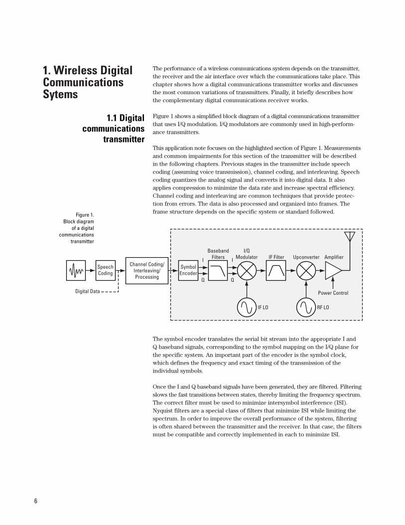
The performance of a wireless communications system depends on the transmitter,the receiver and the air interface over which the communications take place. Thischapter shows how a digital communications transmitter works and discussesthe most common variations of transmitters. Finally, it briefly describes howthe complementary digital communications receiver works.
Figure 1 shows a simplified block diagram of a digital communications transmitterthat uses I/Q modulation. I/Q modulators are commonly used in high-perform-ance transmitters.
This application note focuses on the highlighted section of Figure 1. Measurementsand common impairments for this section of the transmitter will be describedin the following chapters. Previous stages in the transmitter include speechcoding (assuming voice transmission), channel coding, and interleaving. Speechcoding quantizes the analog signal and converts it into digital data. It alsoapplies compression to minimize the data rate and increase spectral efficiency.Channel coding and interleaving are common techniques that provide protec-tion from errors. The data is also processed and organized into frames. Theframe structure depends on the specific system or standard followed.
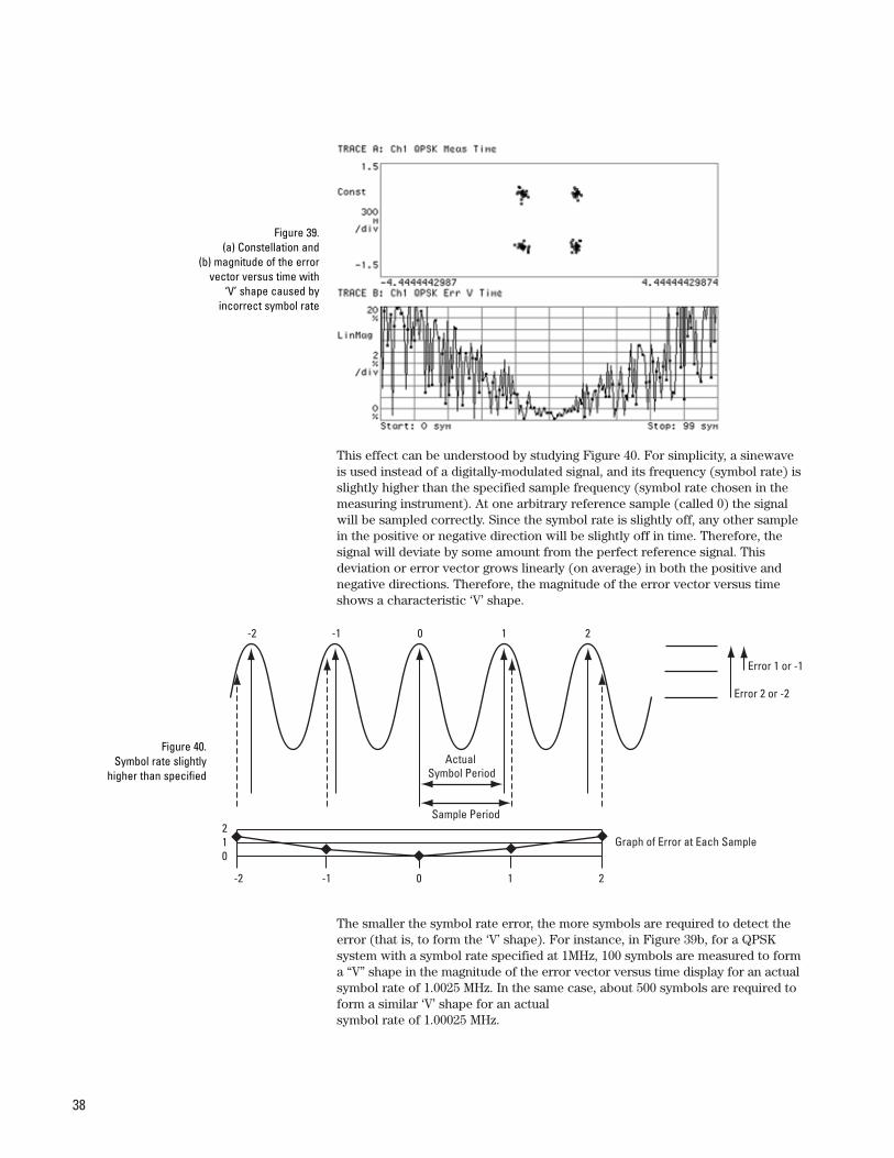
The symbol encoder translates the serial bit stream into the appropriate I andQ baseband signals, corresponding to the symbol mapping on the I/Q plane forthe specific system. An important part of the encoder is the symbol clock,which defines the frequency and exact timing of the transmission of the individual symbols.
Once the I and Q baseband signals have been generated, they are filtered. Filteringslows the fast transitions between states, thereby limiting the frequency spectrum.The correct filter must be used to minimize intersymbol interference (ISI).Nyquist filters are a special class of filters that minimize ISI while limiting thespectrum. In order to improve the overall performance of the system, filteringis often shared between the transmitter and the receiver. In that case, the filtersmust be compatible and correctly implemented in each to minimize ISI.
1. Wireless DigitalCommunicationsSytems
SymbolEncoder
SpeechCoding
Channel Coding/Interleaving/Processing
RF LO
UpconverterBaseband
Filters IF FilterI
Q
I/QModulator
Digital Data
IF LO
I
Q
Amplifier
Power Control
Figure 1.Block diagram
of a digital communications
transmitter
1.1 Digital communications
transmitter
7
The filtered I and Q baseband signals are fed into the I/Q modulator. The localoscillator (LO) in the modulator can operate at an intermediate frequency (IF)or directly at the final radio frequency (RF). The output of the modulator is thecombination of the two orthogonal I and Q signals at IF (or RF). After modulation,the signal is upconverted to RF, if needed.
The RF signal is often combined with other signals (other channels) beforebeing applied to the output amplifier. The amplifier must be appropriate for thesignal type.
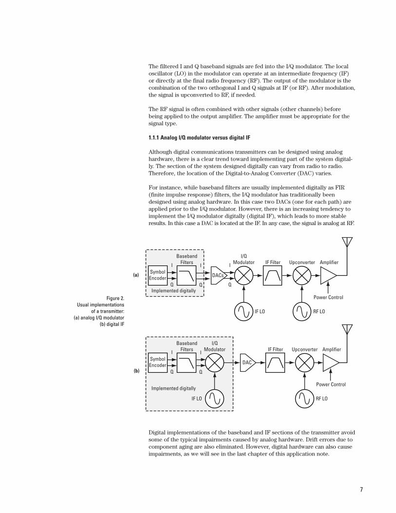
1.1.1 Analog I/Q modulator versus digital IF
Although digital communications transmitters can be designed using analoghardware, there is a clear trend toward implementing part of the system digital-ly. The section of the system designed digitally can vary from radio to radio.Therefore, the location of the Digital-to-Analog Converter (DAC) varies.
For instance, while baseband filters are usually implemented digitally as FIR(finite impulse response) filters, the I/Q modulator has traditionally beendesigned using analog hardware. In this case two DACs (one for each path) areapplied prior to the I/Q modulator. However, there is an increasing tendency toimplement the I/Q modulator digitally (digital IF), which leads to more stableresults. In this case a DAC is located at the IF. In any case, the signal is analog at RF.
Digital implementations of the baseband and IF sections of the transmitter avoidsome of the typical impairments caused by analog hardware. Drift errors due tocomponent aging are also eliminated. However, digital hardware can also causeimpairments, as we will see in the last chapter of this application note.
SymbolEncoder
RF LO
UpconverterBaseband
Filters IF FilterI
Q
I/QModulator
IF LO
DAC
I
Q
Implemented digitally
SymbolEncoder
RF LO
UpconverterBaseband
Filters IF FilterI
Q
I/QModulator
IF LO
I
Q
DACs
I
QImplemented digitally
(a)
(b)
Amplifier
Power Control
Amplifier
Power Control
Figure 2.Usual implementations
of a transmitter: (a) analog I/Q modulator
(b) digital IF
8
1.1.2 Other implementations
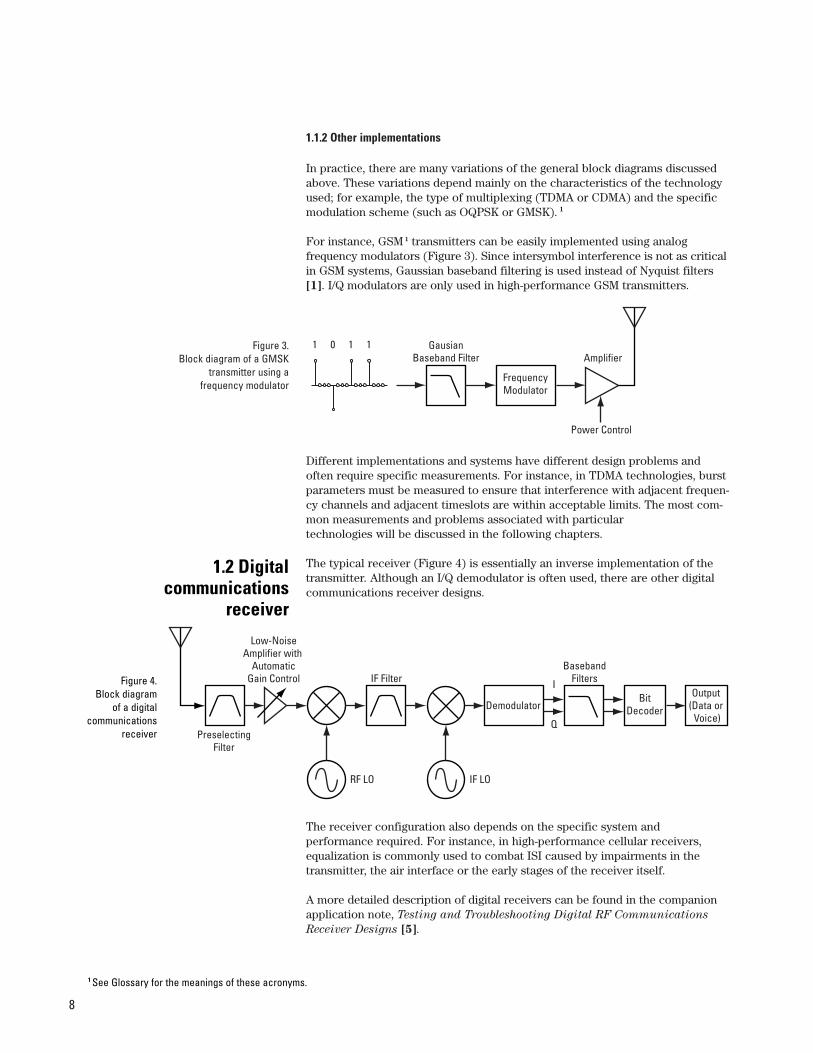
In practice, there are many variations of the general block diagrams discussedabove. These variations depend mainly on the characteristics of the technologyused; for example, the type of multiplexing (TDMA or CDMA) and the specific modulation scheme (such as OQPSK or GMSK). 1
For instance, GSM 1 transmitters can be easily implemented using analog frequency modulators (Figure 3). Since intersymbol interference is not as criticalin GSM systems, Gaussian baseband filtering is used instead of Nyquist filters[1]. I/Q modulators are only used in high-performance GSM transmitters.
Different implementations and systems have different design problems andoften require specific measurements. For instance, in TDMA technologies, burstparameters must be measured to ensure that interference with adjacent frequen-cy channels and adjacent timeslots are within acceptable limits. The most com-mon measurements and problems associated with particular technologies will be discussed in the following chapters.
The typical receiver (Figure 4) is essentially an inverse implementation of thetransmitter. Although an I/Q demodulator is often used, there are other digitalcommunications receiver designs.
The receiver configuration also depends on the specific system and performance required. For instance, in high-performance cellular receivers,equalization is commonly used to combat ISI caused by impairments in thetransmitter, the air interface or the early stages of the receiver itself.
A more detailed description of digital receivers can be found in the companionapplication note, Testing and Troubleshooting Digital RF Communications
Receiver Designs [5].
Figure 3. Block diagram of a GMSK
transmitter using a frequency modulator
FrequencyModulator
GausianBaseband Filter
1 0 1 1Amplifier
Power Control
IF LO
IF Filter
RF LO
BasebandFilters
DemodulatorBit
Decoder
Output (Data or
Voice)
I
Q
Low-NoiseAmplifier with
AutomaticGain Control
PreselectingFilter
Figure 4. Block diagram
of a digital communications
receiver
1 See Glossary for the meanings of these acronyms.
1.2 Digital communications
receiver
9
There are several testing stages during the design of a digital communicationstransmitter. The different components and subsections are initially tested indi-vidually. When appropriate, the transmitter is fully assembled, and system testsare performed. During the design stage of product development, verificationtests are rigorous to make sure that the design is robust. These rigorous confor-mance tests verify that the design meets system requirements, thereby ensuringinteroperability with equipment from different manufacturers.
This chapter covers testing of the highlighted part of the transmitter in Figure 1.It describes the conformance tests and other common measurements made at theantenna port. Most of the transmitter measurements are common to all digitalcommunications technologies, although there are some variations in the way themeasurements are performed. Particular technologies, such as CDMA or TDMA,require specific tests that are also described.
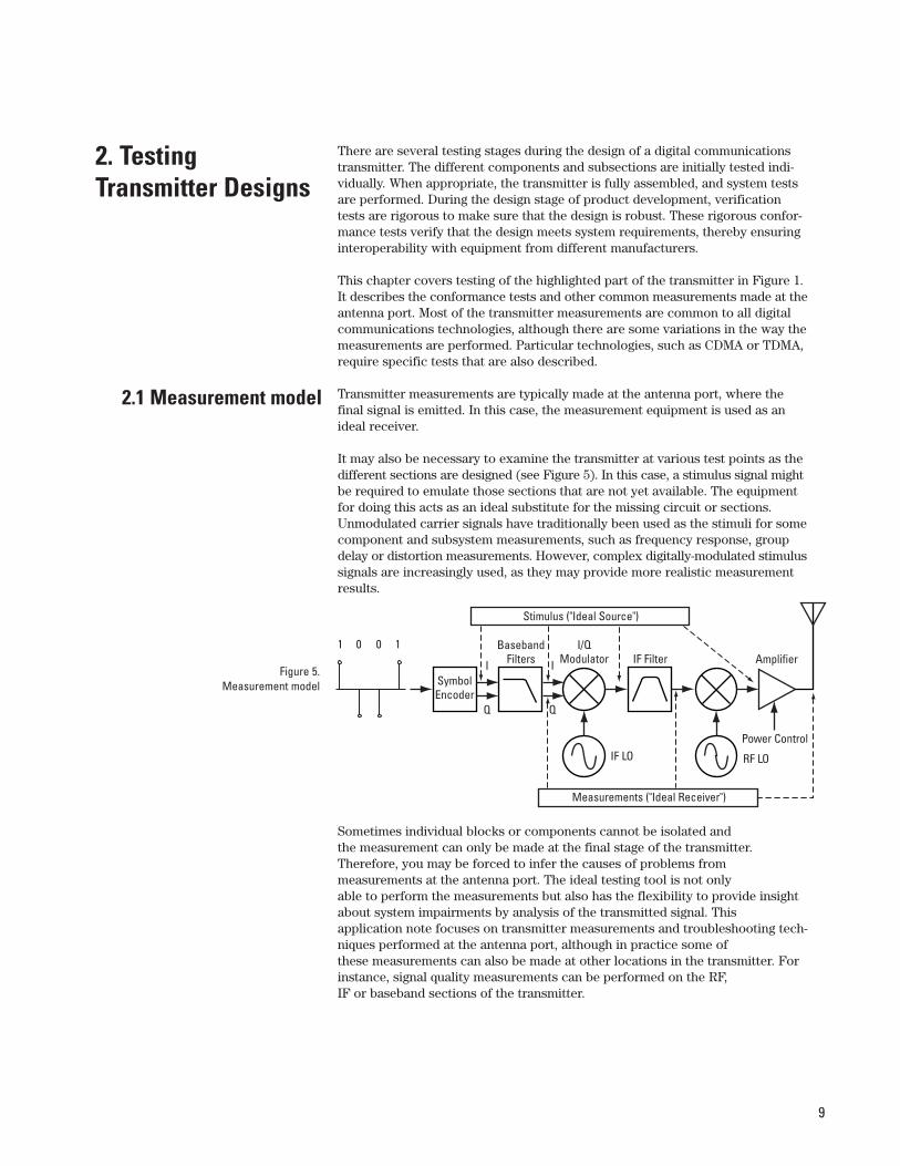
Transmitter measurements are typically made at the antenna port, where thefinal signal is emitted. In this case, the measurement equipment is used as anideal receiver.
It may also be necessary to examine the transmitter at various test points as thedifferent sections are designed (see Figure 5). In this case, a stimulus signal mightbe required to emulate those sections that are not yet available. The equipmentfor doing this acts as an ideal substitute for the missing circuit or sections.Unmodulated carrier signals have traditionally been used as the stimuli for somecomponent and subsystem measurements, such as frequency response, groupdelay or distortion measurements. However, complex digitally-modulated stimulussignals are increasingly used, as they may provide more realistic measurementresults.
Sometimes individual blocks or components cannot be isolated and the measurement can only be made at the final stage of the transmitter.Therefore, you may be forced to infer the causes of problems from measurements at the antenna port. The ideal testing tool is not only able to perform the measurements but also has the flexibility to provide insightabout system impairments by analysis of the transmitted signal. This application note focuses on transmitter measurements and troubleshooting tech-niques performed at the antenna port, although in practice some of these measurements can also be made at other locations in the transmitter. Forinstance, signal quality measurements can be performed on the RF, IF or baseband sections of the transmitter.
Figure 5. Measurement model
2. Testing Transmitter Designs
2.1 Measurement model
SymbolEncoder
RF LO
BasebandFilters IF FilterI
Q
I/QModulator
IF LO
I
Q
Stimulus ("Ideal Source")
Measurements ("Ideal Receiver")
1 0 0 1Amplifier
Power Control
10
The transmitted signal can be viewed in different domains. The time, frequencyand modulation domains provide information on different parameters of a signal.The ideal test instrument can make measurements in all three domains.
Two types of transmitter test instruments are discussed: the spectrum analyzer(SA) and the vector signal analyzer (VSA). Their measurement capabilities ineach domain are described in the following sections of this chapter. Refer toAppendix B for a list of spectrum analyzers and vector signal analyzers fromAgilent Technologies and their capabilities for measuring and troubleshootingdigital communications transmitters.
2.2.1 Time domain
Traditionally, looking at an electrical signal meant using an oscilloscope to viewthe signal in the time domain. However, oscilloscopes do not band limit the inputsignal and have limited dynamic range. Vector signal analyzers downconvert thesignal to baseband and sample the I and Q components of the signal. They candisplay the signal in various coordinate systems, such as amplitude versus time,phase versus time, I or Q versus time, and I/Q polar. Swept-tuned spectrum ana-lyzers can display the signal in the time domain as amplitude (envelope of theRF signal) versus time. Their capability can sometimes be extended to measureI and Q.
Time-domain analysis is especially important in TDMA technologies, where theshape and timing of the burst must be measured.
2.2.2 Frequency domain
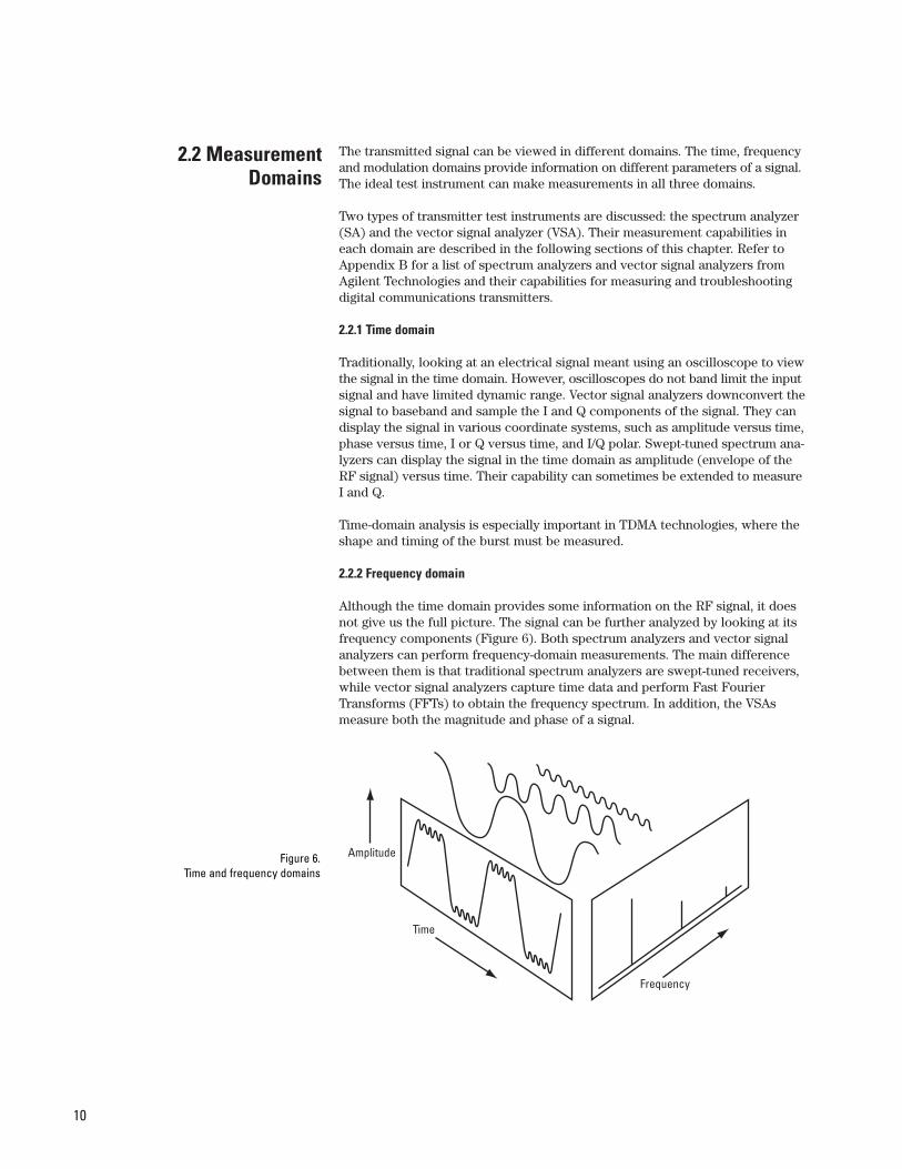
Although the time domain provides some information on the RF signal, it doesnot give us the full picture. The signal can be further analyzed by looking at itsfrequency components (Figure 6). Both spectrum analyzers and vector signalanalyzers can perform frequency-domain measurements. The main differencebetween them is that traditional spectrum analyzers are swept-tuned receivers,while vector signal analyzers capture time data and perform Fast FourierTransforms (FFTs) to obtain the frequency spectrum. In addition, the VSAsmeasure both the magnitude and phase of a signal.
2.2 MeasurementDomains
Time
Amplitude
Frequency
Figure 6.Time and frequency domains
11
Measurements in the frequency domain are especially important to ensure that thesignal meets the spectral occupancy, adjacent channel, and spurious interferencerequirements of the system.
2.2.3 Modulation domain
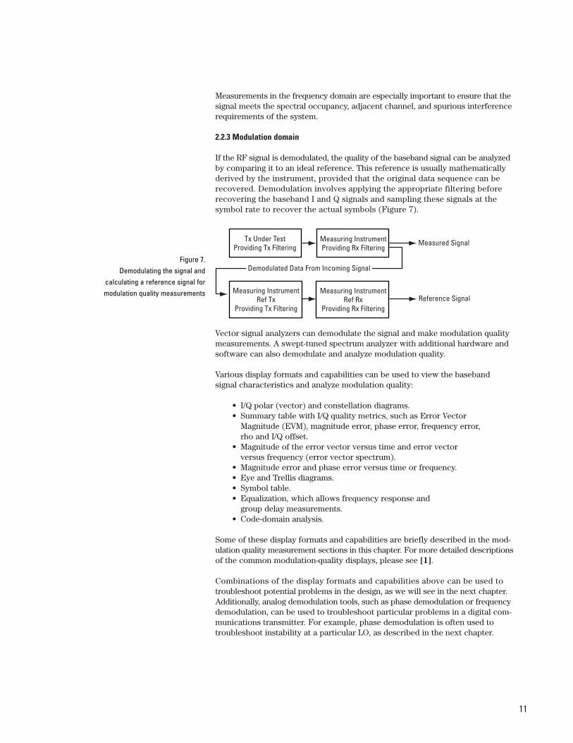
If the RF signal is demodulated, the quality of the baseband signal can be analyzedby comparing it to an ideal reference. This reference is usually mathematicallyderived by the instrument, provided that the original data sequence can berecovered. Demodulation involves applying the appropriate filtering beforerecovering the baseband I and Q signals and sampling these signals at the symbol rate to recover the actual symbols (Figure 7).
Vector signal analyzers can demodulate the signal and make modulation qualitymeasurements. A swept-tuned spectrum analyzer with additional hardware andsoftware can also demodulate and analyze modulation quality.
Various display formats and capabilities can be used to view the baseband signal characteristics and analyze modulation quality:
• I/Q polar (vector) and constellation diagrams.• Summary table with I/Q quality metrics, such as Error Vector
Magnitude (EVM), magnitude error, phase error, frequency error,rho and I/Q offset.
• Magnitude of the error vector versus time and error vector versus frequency (error vector spectrum).
• Magnitude error and phase error versus time or frequency.• Eye and Trellis diagrams.• Symbol table.• Equalization, which allows frequency response and
group delay measurements.• Code-domain analysis.
Some of these display formats and capabilities are briefly described in the mod-ulation quality measurement sections in this chapter. For more detailed descriptionsof the common modulation-quality displays, please see [1].
Combinations of the display formats and capabilities above can be used to troubleshoot potential problems in the design, as we will see in the next chapter.Additionally, analog demodulation tools, such as phase demodulation or frequencydemodulation, can be used to troubleshoot particular problems in a digital com-munications transmitter. For example, phase demodulation is often used totroubleshoot instability at a particular LO, as described in the next chapter.
Tx Under TestProviding Tx Filtering
Measuring InstrumentProviding Rx Filtering
Measuring InstrumentRef Tx
Providing Tx Filtering
Measuring InstrumentRef Rx
Providing Rx Filtering
Measured Signal
Reference Signal
Demodulated Data From Incoming SignalFigure 7.
Demodulating the signal and calculating a reference signal formodulation quality measurements
12
The measurements required to test digital communications transmitters can beclassified as in-band and out-of-band measurements regardless of the technologyused and the standard followed.
In-band measurements are measurements performed within the frequency bandallocated for the system; for example, 890 MHz to 960 MHz for GSM. In-bandmeasurements can be further divided into in-channel and out-of-channel measurements.
2.3.1 In-channel measurements
The definition of channel in digital communications systems depends on the specific technology used. Apart from multiplexing in frequency and space (geography), the common cellular digital communications technologies useeither time or code multiplexing. In TDMA technologies, a channel is defined bya specific frequency and timeslot1 number in a repeating frame1, while in CDMAtechnologies a channel is defined by a specific frequency and code. The termsin-channel and out-of channel refer only to the specific frequency band of interest(frequency channel), and not to the specific timeslot or code channel within thatfrequency band.
2.3.1.1 Channel bandwidth
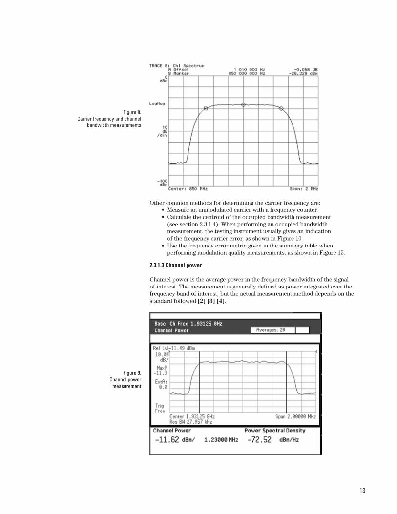
When testing a transmitter, it is usually a good idea to first look at the spectrumof the transmitted signal. The spectrum shape can reveal major errors in thedesign. For a transmitter with a root-raised cosine filter, the 3dB bandwidth ofthe modulated frequency channel should approximate the symbol rate. Forinstance, in Figure 8, for a symbol rate of 1 MHz, the measured 3dB bandwidthis 1.010 MHz. Therefore, this measurement can be used to determine grosserrors in symbol rate.
2.3.1.2 Carrier frequency
Frequency errors can result in interference in the adjacent frequency channels.They can also cause problems in the carrier recovery process of the receiver.The designer must ensure that the transmitter is operating on the correct frequency. The carrier frequency should be located in the center of the spectrumfor most modulation formats. It can be approximated by calculating the centerof the 3dB bandwidth. For instance, in Figure 8, the measured carrier frequencyis 850 MHz.
2.3 In-bandmeasurements
1 See Glossary for definition.
13
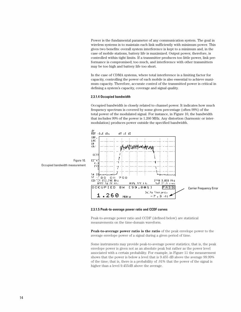
Other common methods for determining the carrier frequency are:• Measure an unmodulated carrier with a frequency counter.• Calculate the centroid of the occupied bandwidth measurement
(see section 2.3.1.4). When performing an occupied bandwidth measurement, the testing instrument usually gives an indication of the frequency carrier error, as shown in Figure 10.
• Use the frequency error metric given in the summary table when performing modulation quality measurements, as shown in Figure 15.
2.3.1.3 Channel power
Channel power is the average power in the frequency bandwidth of the signal of interest. The measurement is generally defined as power integrated over thefrequency band of interest, but the actual measurement method depends on thestandard followed [2] [3] [4].
Figure 8. Carrier frequency and channel
bandwidth measurements
Figure 9. Channel power
measurement
14
Power is the fundamental parameter of any communication system. The goal inwireless systems is to maintain each link sufficiently with minimum power. Thisgives two benefits: overall system interference is kept to a minimum and, in thecase of mobile stations, battery life is maximized. Output power, therefore, iscontrolled within tight limits. If a transmitter produces too little power, link per-formance is compromised; too much, and interference with other transmittersmay be too high and battery life too short.
In the case of CDMA systems, where total interference is a limiting factor forcapacity, controlling the power of each mobile is also essential to achieve maxi-mum capacity. Therefore, accurate control of the transmitted power is critical indefining a system’s capacity, coverage and signal quality.
2.3.1.4 Occupied bandwidth
Occupied bandwidth is closely related to channel power. It indicates how muchfrequency spectrum is covered by some given percentage (often 99%) of thetotal power of the modulated signal. For instance, in Figure 10, the bandwidththat includes 99% of the power is 1.260 MHz. Any distortion (harmonic or inter-modulation) produces power outside the specified bandwidth.
2.3.1.5 Peak-to-average power ratio and CCDF curves
Peak-to-average power ratio and CCDF (defined below) are statistical measurements on the time-domain waveform.
Peak-to-average power ratio is the ratio of the peak envelope power to theaverage envelope power of a signal during a given period of time.
Some instruments may provide peak-to-average power statistics; that is, the peakenvelope power is given not as an absolute peak but rather as the power levelassociated with a certain probability. For example, in Figure 11 the measurementshows that the power is below a level that is 9.455 dB above the average 99.99%of the time; that is, there is a probability of .01% that the power of the signal ishigher than a level 9.455dB above the average.
Figure 10. Occupied bandwidth measurement
Carrier Frequency Error

15
The power statistics of the signal can be completely characterized by performingseveral of these measurements and displaying the results in a graph known asthe Complementary Cumulative Distribution Function (CCDF). The CCDFcurve shows the probability that the power is equal to or above a certain peak-to-average ratio, for different probabilities and peak-to-average ratios. The higherthe peak-to-average power ratio, the lower the probability of reaching it.
Figure 11. Peak-to-average power ratio statistics
Figure 12. CCDF curves
Stop: 20 dBStart: 0 dBm% 0.001%
0.01%
0.1%
1%
10%
TRACE B: Ch1 CCDF
100% Cnt: 736k, Avg: –11.088 dBmCnt: 1.34M, Avg: –11.101 dBm
AWGN Signal(used as a reference)
32-Code Channel Signal
9-Code Channel Signal
Prob
abili
ty
dB Above Average
16
The statistics of the signal determine the headroom required in amplifiers andother components. Signals with different peak-to-average statistics can stressthe components in a transmitter in different ways, causing different levels ofdistortion. CCDF measurements can be performed at different points in thetransmitter to examine the statistics of the signal and the impact of the differentsections on those statistics. These measurements can also be performed at theoutput of the transmitter to compare the statistics to an expected curve. CCDFcurves are also related to Adjacent Channel Power (ACP) measurements, as wewill see later.
Besides causing higher levels of distortion, high peak-to-average ratios can causecumulative damage in some components. Performing CCDF measurements atdifferent points of the transmitter can help you prevent this damage.
Peak-to-average power ratio and CCDF statistic measurements are particularlyimportant in digitally-modulated systems because the statistics may vary. Forinstance, in CDMA systems, the statistics of the signal vary depending on howmany code channels—and which ones—are present at the same time. Figure 12shows the CCDF curves for signals with different code-channel configurations.The more code channels transmitted, the higher the probability of reaching agiven peak-to-average ratio.
In systems that use constant-amplitude modulation schemes, such as GSM, thepeak-to-average ratio of the signal is relevant if the components (for example,the power amplifier) must carry more than one carrier. There is a clear trendtoward using multicarrier power amplifiers in base station designs for most digitalcommunications systems. See [6] for more information on peak-to-averagepower ratio and CCDF curves.
2.3.1.6 Timing measurements
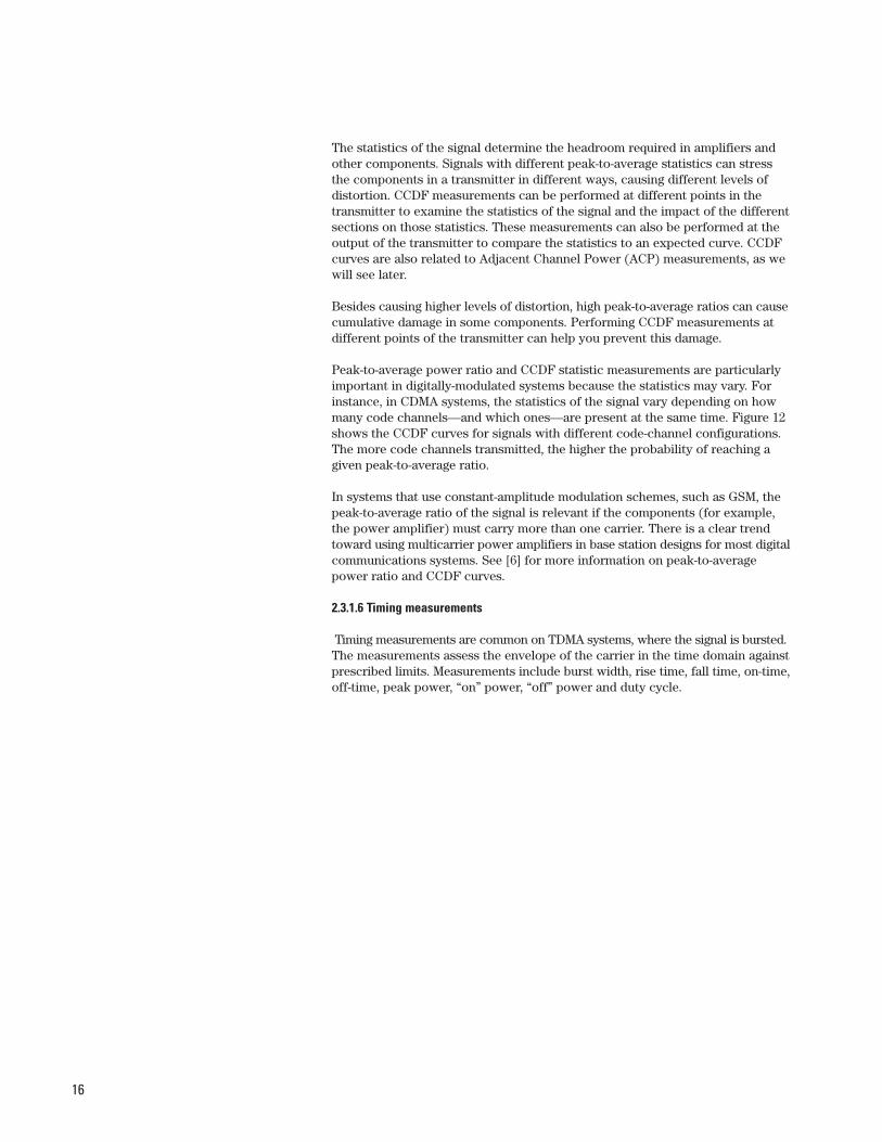
Timing measurements are common on TDMA systems, where the signal is bursted.The measurements assess the envelope of the carrier in the time domain againstprescribed limits. Measurements include burst width, rise time, fall time, on-time,off-time, peak power, “on” power, “off” power and duty cycle.
17
Timing measurements are mainly important to ensure minimum interferencewith adjacent frequency channels or timeslots during signal turn on and turn off.For instance, if the transmitter turns off too slowly, the user of the next timeslotin the TDMA frame experiences interference. If it turns off too quickly, thepower spread into adjacent frequency channels increases [3] [4].
2.3.1.7 Modulation quality measurements
There are a number of different ways to measure the quality of a digitally modu-lated signal. They usually involve precision demodulation of the transmitted signaland comparison of this transmitted signal with a mathematically-generated idealor reference signal, as we saw earlier. The definition of the actual measurementdepends mainly on the modulation scheme and standard followed. NADC andPDC, for example, use Error Vector Magnitude (EVM), while GSM uses phaseand frequency error. cdmaOne uses rho and code-domain power. These andother modulation quality measurements are described in the following sections.
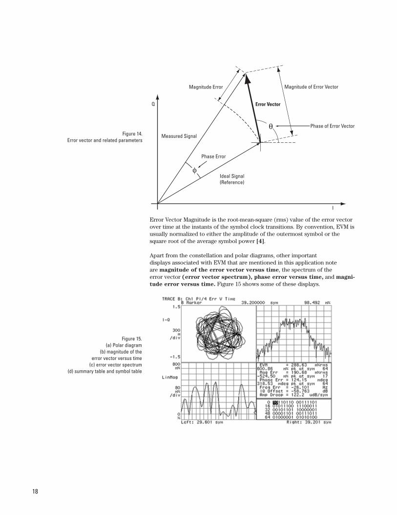
2.3.1.7.1 Error Vector Magnitude (EVM)
The most widely used modulation quality metric in digital communications systemsis Error Vector Magnitude. When performing EVM measurements, the analyzersamples the transmitter output to capture the actual signal trajectory. The signalis usually demodulated and a reference signal is mathematically derived. Theerror vector is the vector difference at a given time between the ideal refer-ence signal and the measured signal. The error vector is a complex quantity thatcontains a magnitude and a phase component. It is important not to confuse themagnitude of the error vector with the magnitude error, or the phase of
the error vector with the phase error. A graphical depiction of these differ-ences can be seen in Figure 14.
Burst Width
Rise Time Fall Time
90% Amplitude Points
50% Amplitude Points
10% Amplitude Points
Off-time
Burst Interval or Period
Average Power
Burst Base Amplitude
Burst Top Amplitude
Peak Power
Overshoot
τ
Figure 13. Timing measurements
18
Error Vector Magnitude is the root-mean-square (rms) value of the error vectorover time at the instants of the symbol clock transitions. By convention, EVM isusually normalized to either the amplitude of the outermost symbol or thesquare root of the average symbol power [4].
Apart from the constellation and polar diagrams, other important displays associated with EVM that are mentioned in this application note are magnitude of the error vector versus time, the spectrum of the error vector (error vector spectrum), phase error versus time, and magni-
tude error versus time. Figure 15 shows some of these displays.
Figure 14. Error vector and related parameters
Figure 15. (a) Polar diagram
(b) magnitude of the error vector versus time
(c) error vector spectrum (d) summary table and symbol table
Q
I
Magnitude Error
Phase of Error Vector
Measured Signal
Ideal Signal(Reference)
Phase Error
Error Vector
Magnitude of Error Vector
θ
φ
19
EVM and the various related displays are sensitive to any signal flaw that affectsthe magnitude and phase trajectory of a signal for any digital modulation format.Large error vectors both at the symbol points and at the transitions betweensymbols can be caused by problems at the baseband, IF or RF sections of thetransmitter. As shown in the last chapter of this application note, the differentmodulation quality displays and tools can help reveal or troubleshoot variousproblems in the transmitter. For instance, the I/Q constellation can be used toeasily identify I/Q gain imbalance errors. Small symbol rate errors can be easilyidentified by looking at the magnitude of the error vector versus time display.The error vector spectrum can help locate in-channel spurious.
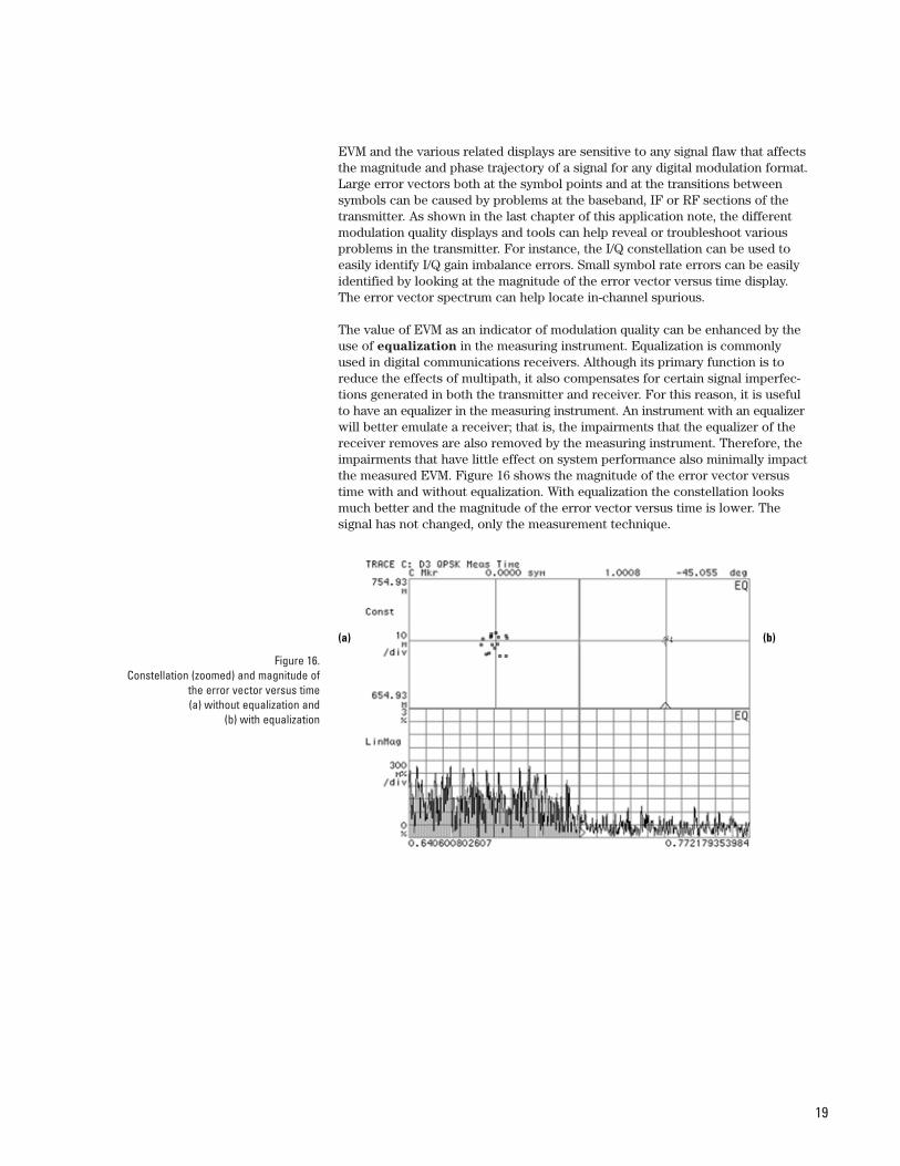
The value of EVM as an indicator of modulation quality can be enhanced by theuse of equalization in the measuring instrument. Equalization is commonlyused in digital communications receivers. Although its primary function is toreduce the effects of multipath, it also compensates for certain signal imperfec-tions generated in both the transmitter and receiver. For this reason, it is usefulto have an equalizer in the measuring instrument. An instrument with an equalizerwill better emulate a receiver; that is, the impairments that the equalizer of thereceiver removes are also removed by the measuring instrument. Therefore, theimpairments that have little effect on system performance also minimally impactthe measured EVM. Figure 16 shows the magnitude of the error vector versustime with and without equalization. With equalization the constellation looksmuch better and the magnitude of the error vector versus time is lower. The signal has not changed, only the measurement technique.
Figure 16.Constellation (zoomed) and magnitude of
the error vector versus time (a) without equalization and
(b) with equalization
(a) (b)
20
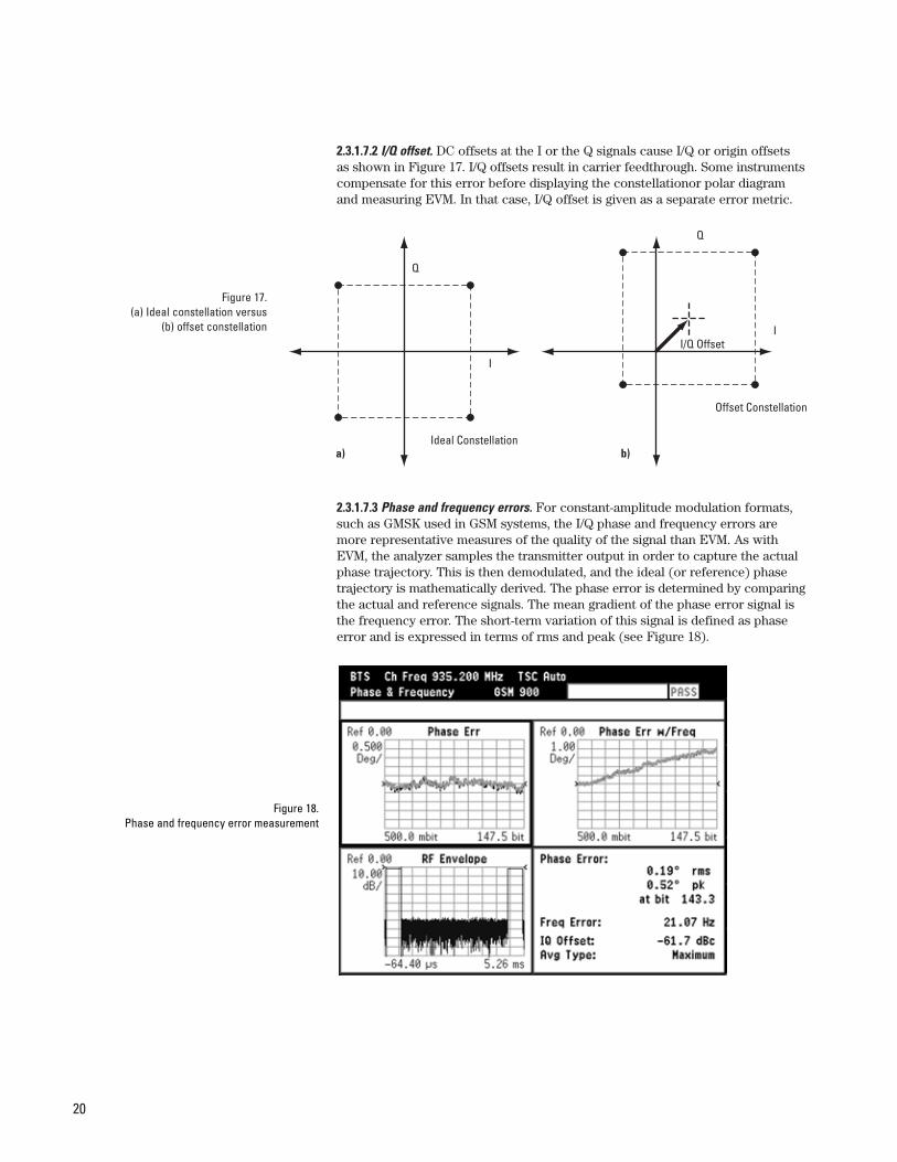
2.3.1.7.2 I/Q offset. DC offsets at the I or the Q signals cause I/Q or origin offsetsas shown in Figure 17. I/Q offsets result in carrier feedthrough. Some instrumentscompensate for this error before displaying the constellationor polar diagramand measuring EVM. In that case, I/Q offset is given as a separate error metric.
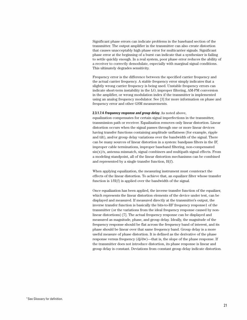
2.3.1.7.3 Phase and frequency errors. For constant-amplitude modulation formats,such as GMSK used in GSM systems, the I/Q phase and frequency errors aremore representative measures of the quality of the signal than EVM. As withEVM, the analyzer samples the transmitter output in order to capture the actualphase trajectory. This is then demodulated, and the ideal (or reference) phasetrajectory is mathematically derived. The phase error is determined by comparingthe actual and reference signals. The mean gradient of the phase error signal isthe frequency error. The short-term variation of this signal is defined as phaseerror and is expressed in terms of rms and peak (see Figure 18).
Figure 17.(a) Ideal constellation versus
(b) offset constellation
Q
I
Ideal Constellation
Q
I
Offset Constellation
I/Q Offset
a) b)
Figure 18. Phase and frequency error measurement
21
Significant phase errors can indicate problems in the baseband section of thetransmitter. The output amplifier in the transmitter can also create distortionthat causes unacceptably high phase error for multicarrier signals. Significantphase error at the beginning of a burst can indicate that a synthesizer is failingto settle quickly enough. In a real system, poor phase error reduces the ability ofa receiver to correctly demodulate, especially with marginal signal conditions.This ultimately degrades sensitivity.
Frequency error is the difference between the specified carrier frequency andthe actual carrier frequency. A stable frequency error simply indicates that aslightly wrong carrier frequency is being used. Unstable frequency errors canindicate short-term instability in the LO, improper filtering, AM-PM conversionin the amplifier, or wrong modulation index if the transmitter is implementedusing an analog frequency modulator. See [3] for more information on phase andfrequency error and other GSM measurements.
2.3.1.7.4 Frequency response and group delay. As noted above, equalization compensates for certain signal imperfections in the transmitter,transmission path or receiver. Equalization removes only linear distortion. Lineardistortion occurs when the signal passes through one or more linear deviceshaving transfer functions containing amplitude unflatness (for example, rippleand tilt), and/or group delay variations over the bandwidth of the signal. Therecan be many sources of linear distortion in a system: bandpass filters in the IF,improper cable terminations, improper baseband filtering, non-compensatedsin(x)/x, antenna mismatch, signal combiners and multipath signal effects. Froma modeling standpoint, all of the linear distortion mechanisms can be combinedand represented by a single transfer function, H(f).
When applying equalization, the measuring instrument must counteract theeffects of the linear distortion. To achieve that, an equalizer filter whose transferfunction is 1/H(f) is applied over the bandwidth of the signal.
Once equalization has been applied, the inverse transfer function of the equalizer,which represents the linear distortion elements of the device under test, can bedisplayed and measured. If measured directly at the transmitter’s output, theinverse transfer function is basically the bits-to-RF frequency response1 of thetransmitter (or the variations from the ideal frequency response caused by non-linear distortions) [7]. The actual frequency response can be displayed andmeasured as magnitude, phase, and group delay. Ideally, the magnitude of thefrequency response should be flat across the frequency band of interest, and itsphase should be linear over that same frequency band. Group delay is a moreuseful measure of phase distortion. It is defined as the derivative of the phaseresponse versus frequency (dj/dw)—that is, the slope of the phase response. Ifthe transmitter does not introduce distortion, its phase response is linear andgroup delay is constant. Deviations from constant group delay indicate distortion.
1 See Glossary for definition.
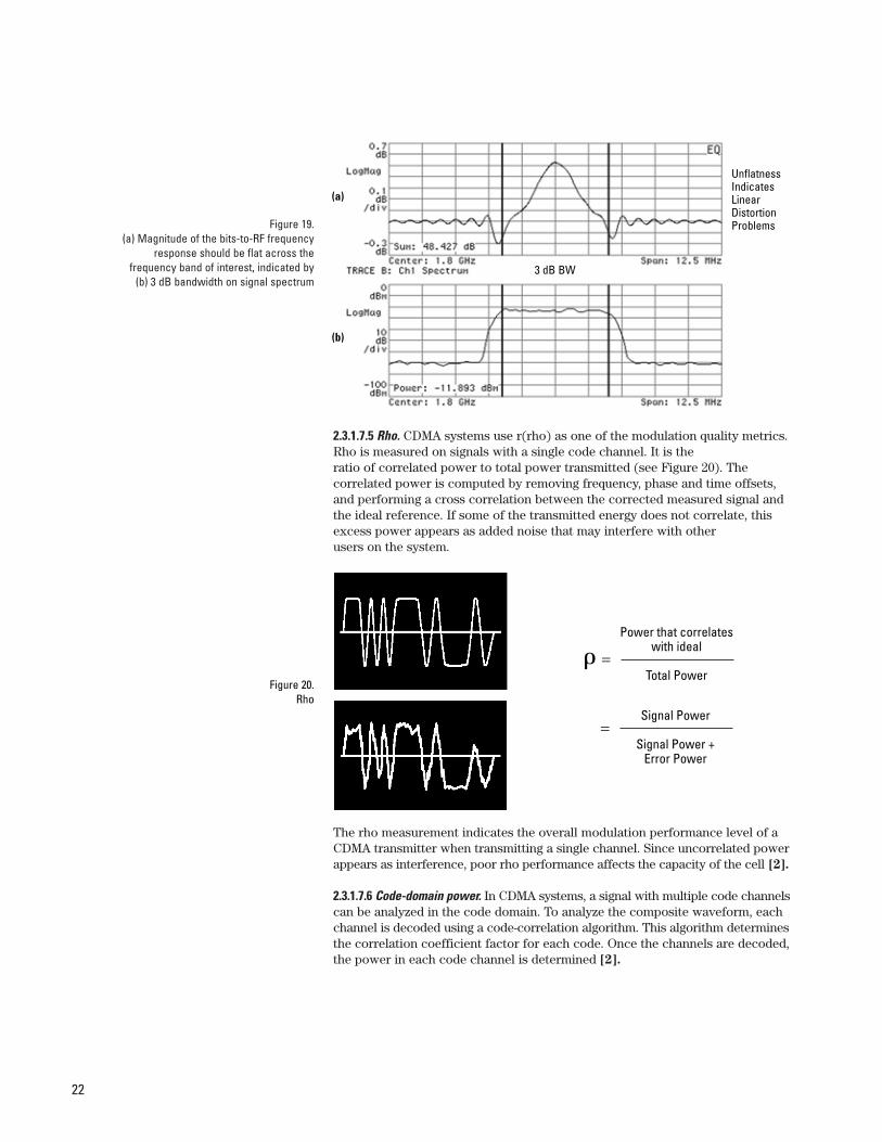
22
2.3.1.7.5 Rho. CDMA systems use r(rho) as one of the modulation quality metrics.Rho is measured on signals with a single code channel. It is the ratio of correlated power to total power transmitted (see Figure 20). The correlated power is computed by removing frequency, phase and time offsets,and performing a cross correlation between the corrected measured signal andthe ideal reference. If some of the transmitted energy does not correlate, thisexcess power appears as added noise that may interfere with other users on the system.
The rho measurement indicates the overall modulation performance level of aCDMA transmitter when transmitting a single channel. Since uncorrelated powerappears as interference, poor rho performance affects the capacity of the cell [2].
2.3.1.7.6 Code-domain power. In CDMA systems, a signal with multiple code channelscan be analyzed in the code domain. To analyze the composite waveform, eachchannel is decoded using a code-correlation algorithm. This algorithm determinesthe correlation coefficient factor for each code. Once the channels are decoded,the power in each code channel is determined [2].
Figure 19. (a) Magnitude of the bits-to-RF frequency
response should be flat across the frequency band of interest, indicated by
(b) 3 dB bandwidth on signal spectrum
Figure 20.Rho
Unflatness Indicates Linear Distortion Problems
(a)
(b)
3 dB BW
Power that correlateswith ideal
Total Power
Signal Power
Signal Power +Error Power
23
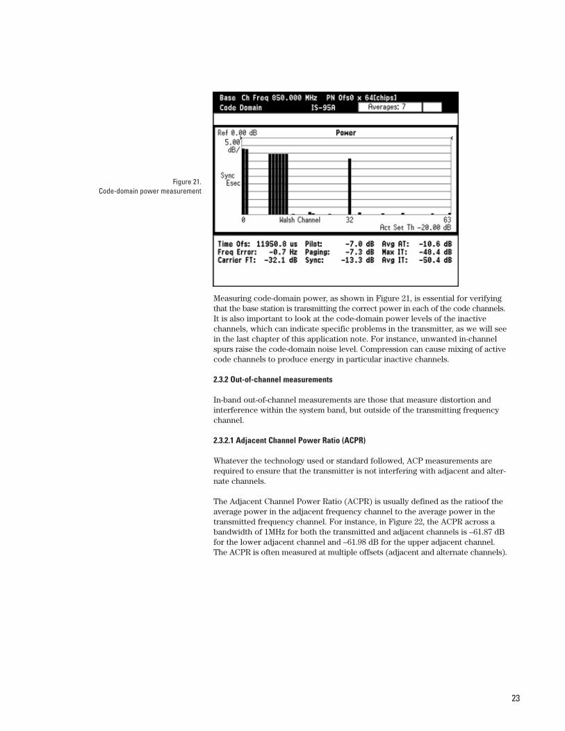
Measuring code-domain power, as shown in Figure 21, is essential for verifyingthat the base station is transmitting the correct power in each of the code channels.It is also important to look at the code-domain power levels of the inactivechannels, which can indicate specific problems in the transmitter, as we will seein the last chapter of this application note. For instance, unwanted in-channelspurs raise the code-domain noise level. Compression can cause mixing of activecode channels to produce energy in particular inactive channels.
2.3.2 Out-of-channel measurements
In-band out-of-channel measurements are those that measure distortion andinterference within the system band, but outside of the transmitting frequencychannel.
2.3.2.1 Adjacent Channel Power Ratio (ACPR)
Whatever the technology used or standard followed, ACP measurements arerequired to ensure that the transmitter is not interfering with adjacent and alter-nate channels.
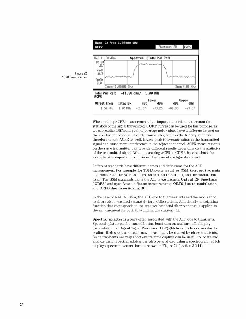
The Adjacent Channel Power Ratio (ACPR) is usually defined as the ratioof theaverage power in the adjacent frequency channel to the average power in thetransmitted frequency channel. For instance, in Figure 22, the ACPR across abandwidth of 1MHz for both the transmitted and adjacent channels is –61.87 dBfor the lower adjacent channel and –61.98 dB for the upper adjacent channel.The ACPR is often measured at multiple offsets (adjacent and alternate channels).
Figure 21. Code-domain power measurement
24
When making ACPR measurements, it is important to take into account the statistics of the signal transmitted. CCDF curves can be used for this purpose, aswe saw earlier. Different peak-to-average ratio values have a different impact onthe non-linear components of the transmitter, such as the RF amplifier, andtherefore on the ACPR as well. Higher peak-to-average ratios in the transmittedsignal can cause more interference in the adjacent channel. ACPR measurementson the same transmitter can provide different results depending on the statisticsof the transmitted signal. When measuring ACPR in CDMA base stations, forexample, it is important to consider the channel configuration used.
Different standards have different names and definitions for the ACP measurement. For example, for TDMA systems such as GSM, there are two maincontributors to the ACP: the burst-on and -off transitions, and the modulationitself. The GSM standards name the ACP measurement Output RF Spectrum
(ORFS) and specify two different measurements: ORFS due to modulation
and ORFS due to switching [3].
In the case of NADC-TDMA, the ACP due to the transients and the modulationitself are also measured separately for mobile stations. Additionally, a weightingfunction that corresponds to the receiver baseband filter response is applied tothe measurement for both base and mobile stations [4].
Spectral splatter is a term often associated with the ACP due to transients.Spectral splatter can be caused by fast burst turn-on and turn-off, clipping (saturation) and Digital Signal Processor (DSP) glitches or other errors due toscaling. High spectral splatter may occasionally be caused by phase transients.Since transients are very short events, time capture can be useful to locate andanalyze them. Spectral splatter can also be analyzed using a spectrogram, whichdisplays spectrum versus time, as shown in Figure 74 (section 3.2.11).
Figure 22. ACPR measurement
25
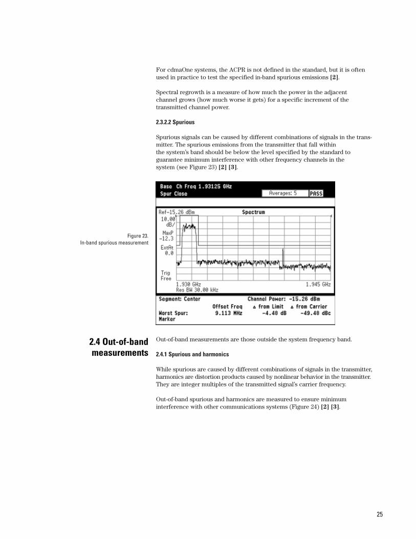
For cdmaOne systems, the ACPR is not defined in the standard, but it is oftenused in practice to test the specified in-band spurious emissions [2].
Spectral regrowth is a measure of how much the power in the adjacent channel grows (how much worse it gets) for a specific increment of the transmitted channel power.
2.3.2.2 Spurious
Spurious signals can be caused by different combinations of signals in the trans-mitter. The spurious emissions from the transmitter that fall within the system’s band should be below the level specified by the standard to guarantee minimum interference with other frequency channels in the system (see Figure 23) [2] [3].
Out-of-band measurements are those outside the system frequency band.
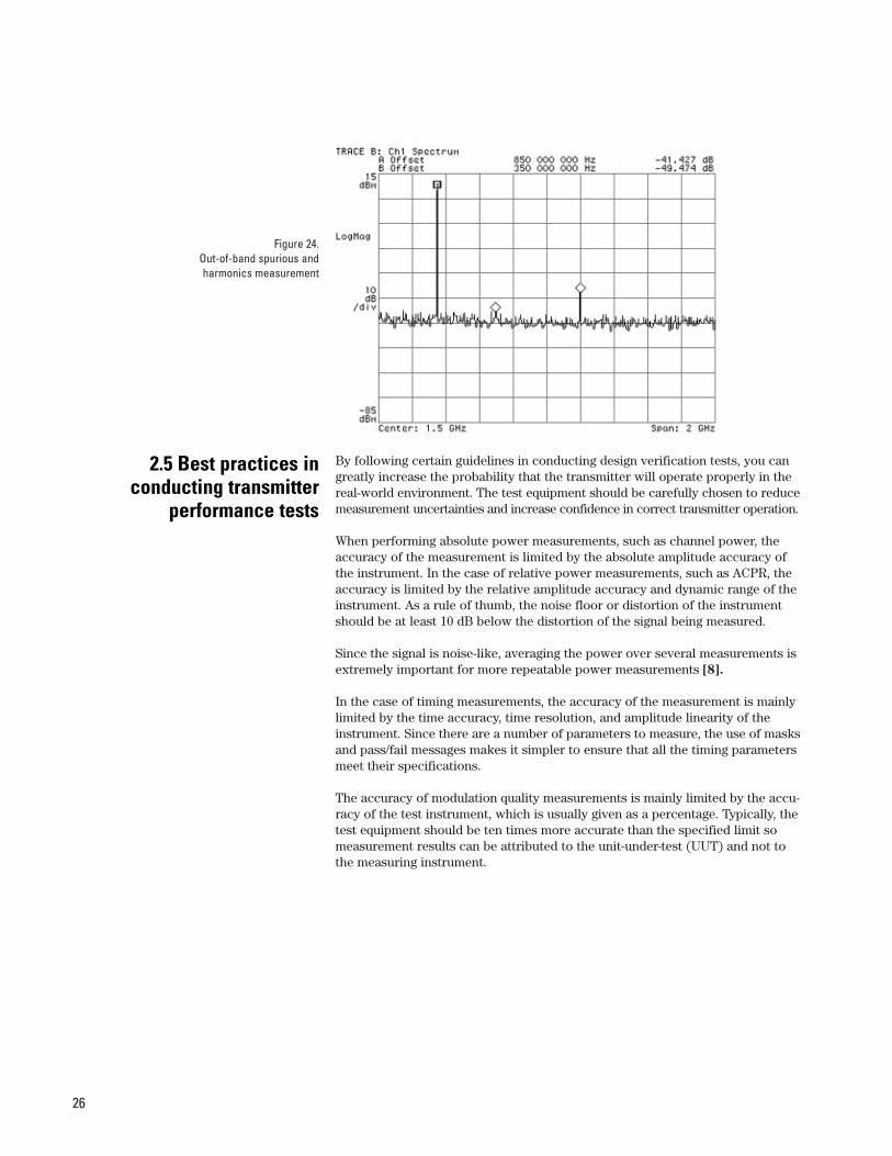
2.4.1 Spurious and harmonics
While spurious are caused by different combinations of signals in the transmitter,harmonics are distortion products caused by nonlinear behavior in the transmitter.They are integer multiples of the transmitted signal’s carrier frequency.
Out-of-band spurious and harmonics are measured to ensure minimum interference with other communications systems (Figure 24) [2] [3].
Figure 23.In-band spurious measurement
2.4 Out-of-bandmeasurements
26
By following certain guidelines in conducting design verification tests, you cangreatly increase the probability that the transmitter will operate properly in thereal-world environment. The test equipment should be carefully chosen to reducemeasurement uncertainties and increase confidence in correct transmitter operation.
When performing absolute power measurements, such as channel power, theaccuracy of the measurement is limited by the absolute amplitude accuracy ofthe instrument. In the case of relative power measurements, such as ACPR, theaccuracy is limited by the relative amplitude accuracy and dynamic range of theinstrument. As a rule of thumb, the noise floor or distortion of the instrumentshould be at least 10 dB below the distortion of the signal being measured.
Since the signal is noise-like, averaging the power over several measurements isextremely important for more repeatable power measurements [8].
In the case of timing measurements, the accuracy of the measurement is mainlylimited by the time accuracy, time resolution, and amplitude linearity of theinstrument. Since there are a number of parameters to measure, the use of masksand pass/fail messages makes it simpler to ensure that all the timing parametersmeet their specifications.
The accuracy of modulation quality measurements is mainly limited by the accu-racy of the test instrument, which is usually given as a percentage. Typically, thetest equipment should be ten times more accurate than the specified limit someasurement results can be attributed to the unit-under-test (UUT) and not tothe measuring instrument.
Figure 24. Out-of-band spurious andharmonics measurement
2.5 Best practices inconducting transmitter
performance tests
27
Transmitter designs are tested to ensure conformance with a particular standardand are typically performed at the antenna port. However, substandard performancemay be caused by various parts of the system, so troubleshooting is usually doneat several points in the transmitter. The source of impairments can be difficult todetermine. This difficulty is magnified by these practicalities:
• Part of the transmitter is generally implemented digitally.• Some parts of the transmitter may not be accessible.• It may be unclear whether a problem is rooted in the analog or digital
section of the system.
The ability to look at the signal and deduce the source of a problem is veryimportant to successful design. The ideal troubleshooting instrument has theflexibility and measurement capabilities to help you infer problem causes frommeasurements at the RF, IF and baseband sections of the transmitter.
The measurements described in this chapter are performed at the antenna port,assuming that other parts of the transmitter are not easily accessed. The objectiveis to help you recognize and troubleshoot the most common impairments frommeasurements performed at the antenna port. To assist you in this task, the fol-lowing information is included in this chapter:
• A general troubleshooting procedure (see Appendix A for a more detailed procedure).
• A table that links measurement problems to their possible causes in the different sections of the transmitter.
• A description of the most common impairments, and an explanation of how to verify each one of them.
The following is a suggested troubleshooting procedure to follow if the transmitterdesign does not meet the specifications:
1. Look at the signal in the frequency domain and verify that its spectrum appears as expected. Ensure that its center frequency and bandwidth are correct.
2. Perform in-band and out-of-band power measurements: channel power, ACP (check CCDF curve), spurious and harmonics.
3. In the case of bursted signals, perform timing measurements.4. Look at the constellation of the baseband signal.5. Examine error metrics (EVM, I/Q offsets, phase error, frequency error,
magnitude error and rho).6. If the phase error is significantly larger than the magnitude error, examine
I/Q phase error versus time. Perform phase noise measurements on LOs, if accessible.
7. If phase error and magnitude error are comparable, examine magnitude of the error vector versus time and error vector spectrum.
8. Turn the equalizer on and verify that it reduces modulation quality errors,and check frequency response and group delay of the transmitter for faulty baseband or IF filtering or other linear distortion problems.
3. TroubleshootingTransmitter Designs
3.1 Troubleshooting procedure
28
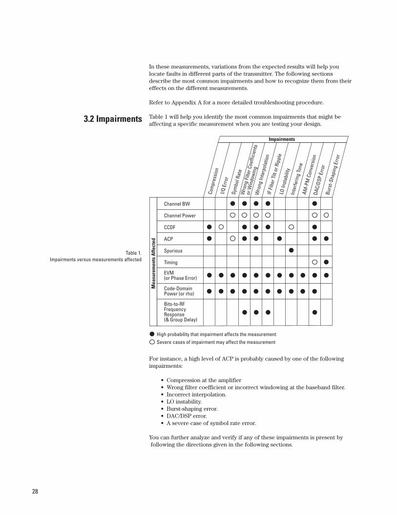
In these measurements, variations from the expected results will help youlocate faults in different parts of the transmitter. The following sectionsdescribe the most common impairments and how to recognize them from theireffects on the different measurements.
Refer to Appendix A for a more detailed troubleshooting procedure.
Table 1 will help you identify the most common impairments that might beaffecting a specific measurement when you are testing your design.
For instance, a high level of ACP is probably caused by one of the followingimpairments:
• Compression at the amplifier• Wrong filter coefficient or incorrect windowing at the baseband filter. • Incorrect interpolation.• LO instability.• Burst-shaping error.• DAC/DSP error.• A severe case of symbol rate error.
You can further analyze and verify if any of these impairments is present byfollowing the directions given in the following sections.
Table 1. Impairments versus measurements affected
3.2 Impairments
Channel BW
Channel Power
CCDF
ACP
Spurious
Timing
EVM(or Phase Error)
Code-DomainPower (or rho)
Bits-to-RFFrequencyResponse(& Group Delay)
Com
pres
sion
I/Q
Err
or
Sym
bol R
ate
Wro
ng F
ilter
Coe
ffici
ents
or W
indo
win
g
Wro
ng In
terp
olat
ion
IF F
ilter
Tilt
or R
ippl
e
LO
Inst
abili
ty
In
terfe
ring
Tone
AM
-PM
Con
vers
ion
D
AC/D
SP E
rror
Bur
st-S
hapi
ng E
rror
Impairments
Mea
sure
men
ts A
ffect
ed
High probability that impairment affects the measurementSevere cases of impairment may affect the measurement
29
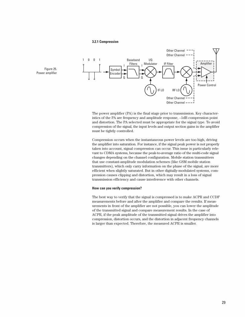
3.2.1 Compression
The power amplifier (PA) is the final stage prior to transmission. Key character-istics of the PA are frequency and amplitude response, –1dB compression pointand distortion. The PA selected must be appropriate for the signal type. To avoidcompression of the signal, the input levels and output section gains in the amplifiermust be tightly controlled.
Compression occurs when the instantaneous power levels are too high, drivingthe amplifier into saturation. For instance, if the signal peak power is not properlytaken into account, signal compression can occur. This issue is particularly rele-vant to CDMA systems, because the peak-to-average ratio of the multi-code signalchanges depending on the channel configuration. Mobile station transmittersthat use constant-amplitude modulation schemes (like GSM mobile stationtransmitters), which only carry information on the phase of the signal, are moreefficient when slightly saturated. But in other digitally-modulated systems, com-pression causes clipping and distortion, which may result in a loss of signaltransmission efficiency and cause interference with other channels.
How can you verify compression?
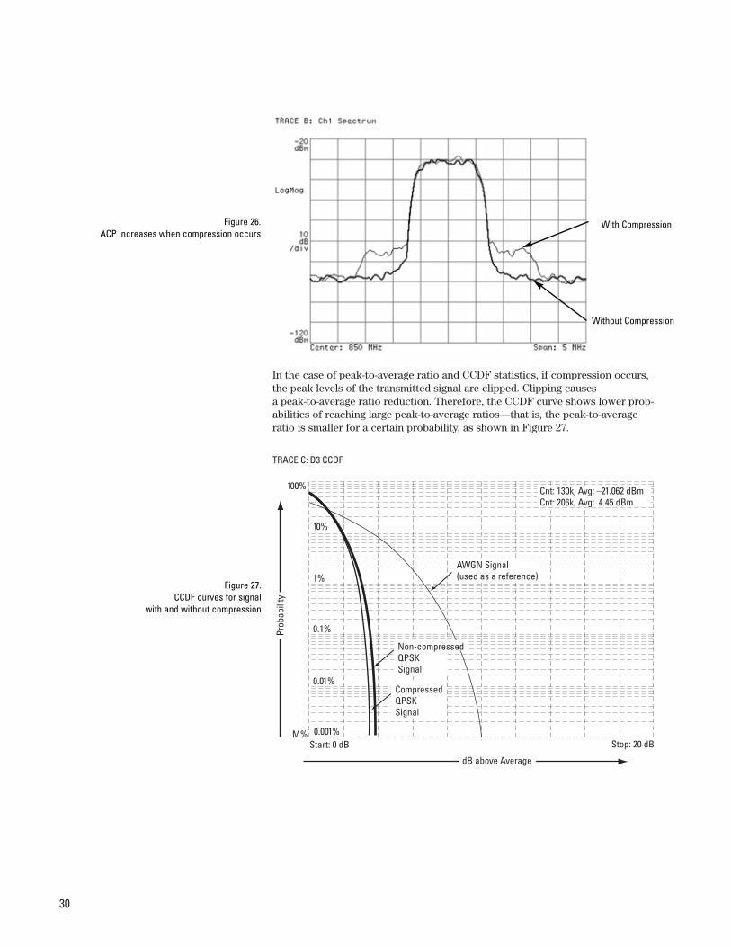
The best way to verify that the signal is compressed is to make ACPR and CCDFmeasurements before and after the amplifier and compare the results. If meas-urements in front of the amplifier are not possible, you can lower the amplitudeof the transmitted signal and compare measurement results. In the case ofACPR, if the peak amplitude of the transmitted signal drives the amplifier intocompression, distortion occurs, and the distortion in adjacent frequency channelsis larger than expected. Therefore, the measured ACPR is smaller.
Figure 25. Power amplifier
SymbolEncoder
RF LO
BasebandFilters IF FilterI
Q
I/QModulator
IF LO
I
Q
Other ChannelOther Channel
Other ChannelOther Channel
1 0 0 1Amplifier
Power Control
30
In the case of peak-to-average ratio and CCDF statistics, if compression occurs,the peak levels of the transmitted signal are clipped. Clipping causes a peak-to-average ratio reduction. Therefore, the CCDF curve shows lower prob-abilities of reaching large peak-to-average ratios—that is, the peak-to-averageratio is smaller for a certain probability, as shown in Figure 27.
Figure 26. ACP increases when compression occurs
Stop: 20 dBStart: 0 dBM% 0.001%
0.01%
0.1%
1%
10%
TRACE C: D3 CCDF
100% Cnt: 130k, Avg: –21.062 dBmCnt: 206k, Avg: 4.45 dBm
AWGN Signal(used as a reference)
Prob
abili
ty
dB above Average
Compressed QPSKSignal
Non-compressed QPSKSignal
Figure 27. CCDF curves for signal
with and without compression
With Compression
Without Compression
31
Compression may also be detected in other measurements:
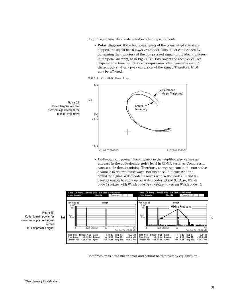
• Polar diagram. If the high peak levels of the transmitted signal are clipped, the signal has a lower overshoot. This effect can be seen by comparing the trajectory of the compressed signal to the ideal trajectory in the polar diagram, as in Figure 28. Filtering at the receiver causes dispersion in time. In practice, compression often causes an error in the symbol(s) after a peak excursion of the signal. Therefore, EVM may be affected.
• Code-domain power. Non-linearity in the amplifier also causes an increase in the code-domain noise level in CDMA systems. Compression causes code-domain mixing. Therefore, energy appears in the non-active channels in deterministic ways. For instance, in Figure 29, for a cdmaOne signal, Walsh code 1 1 mixes with Walsh codes 12 and 32, causing energy to show up on Walsh codes 13 and 33. Also, Walsh code 12 mixes with Walsh code 32 to create power on Walsh code 44.
Compression is not a linear error and cannot be removed by equalization.
Figure 28.Polar diagram of com-
pressed signal (comparedto ideal trajectory)
Figure 29. Code-domain power for
(a) non-compressed signalversus
(b) compressed signal
1 See Glossary for definition.
(a) (b)
ActualTrajectory
Reference (Ideal Trajectory)
Mixing Products
32
I/Q Impairments
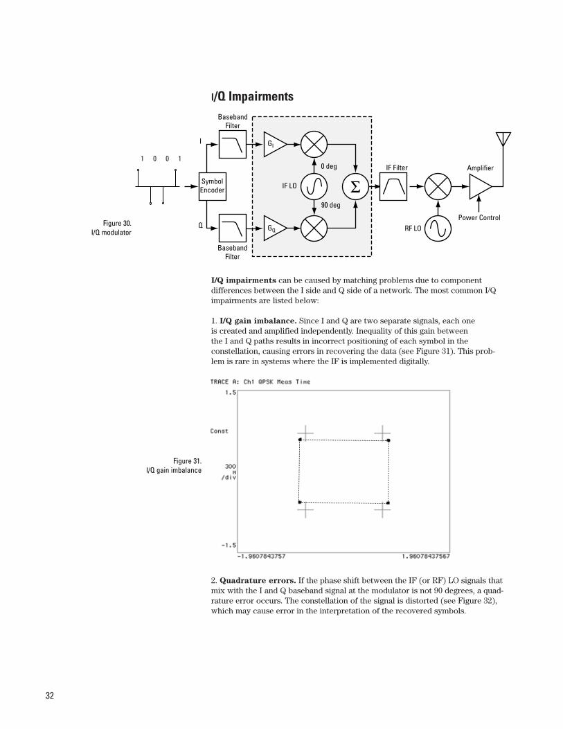
I/Q impairments can be caused by matching problems due to component differences between the I side and Q side of a network. The most common I/Qimpairments are listed below:
1. I/Q gain imbalance. Since I and Q are two separate signals, each one is created and amplified independently. Inequality of this gain between the I and Q paths results in incorrect positioning of each symbol in the constellation, causing errors in recovering the data (see Figure 31). This prob-lem is rare in systems where the IF is implemented digitally.
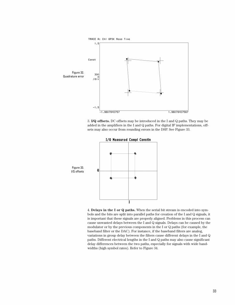
2. Quadrature errors. If the phase shift between the IF (or RF) LO signals thatmix with the I and Q baseband signal at the modulator is not 90 degrees, a quad-rature error occurs. The constellation of the signal is distorted (see Figure 32),which may cause error in the interpretation of the recovered symbols.
SymbolEncoder
RF LO
IF Filter
I
Q
BasebandFilter
BasebandFilter
IF LO
0 deg
90 deg
GQ
GI
ΣAmplifier
Power Control
1 0 0 1
Figure 30.I/Q modulator
Figure 31. I/Q gain imbalance
33
3. I/Q offsets. DC offsets may be introduced in the I and Q paths. They may beadded in the amplifiers in the I and Q paths. For digital IF implementations, off-sets may also occur from rounding errors in the DSP. See Figure 33.
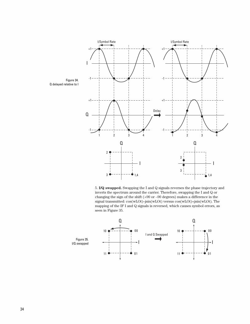
4. Delays in the I or Q paths. When the serial bit stream is encoded into sym-bols and the bits are split into parallel paths for creation of the I and Q signals, itis important that these signals are properly aligned. Problems in this process cancause unwanted delays between the I and Q signals. Delays can be caused by themodulator or by the previous components in the I or Q paths (for example, thebaseband filter or the DAC). For instance, if the baseband filters are analog, variations in group delay between the filters cause different delays in the I and Qpaths. Different electrical lengths in the I and Q paths may also cause significantdelay differences between the two paths, especially for signals with wide band-widths (high symbol rates). Refer to Figure 34.
Figure 32. Quadrature error
Figure 33. I/Q offsets
34
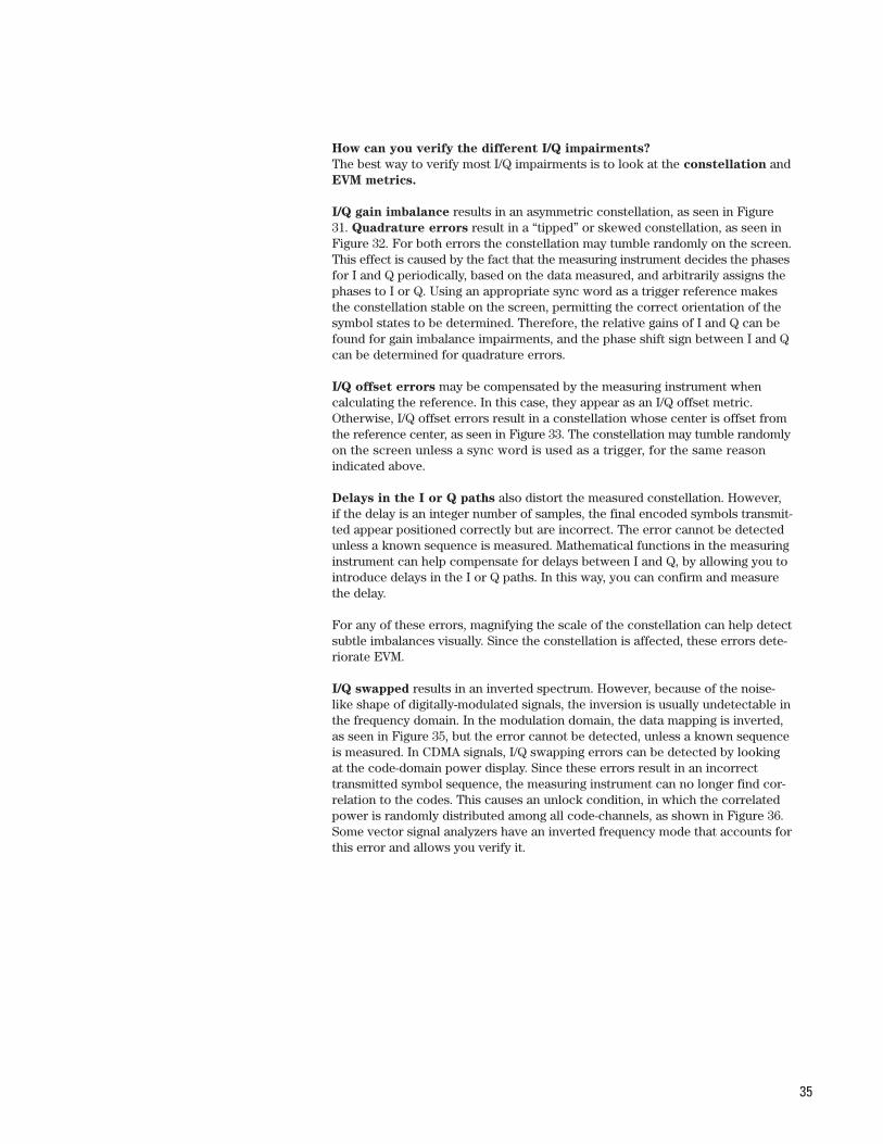
5. I/Q swapped. Swapping the I and Q signals reverses the phase trajectory andinverts the spectrum around the carrier. Therefore, swapping the I and Q orchanging the sign of the shift (+90 or –90 degrees) makes a difference in the signal transmitted: cos(wLOt)–jsin(wLOt) versus cos(wLOt)+jsin(wLOt). Themapping of the IF I and Q signals is reversed, which causes symbol errors, asseen in Figure 35.
2
3 1,4
Q
I
1 2 3 4
Q
-1
+1
I
-1
+1
I/Symbol Rate
2
31,4
Q
I
1 2 3 4
-1
+1
-1
+1
I/Symbol Rate
Delay
Figure 34. Q delayed relative to I
10 00
11 01
I and Q Swapped
Q
I
10 00
11 01
Q
IFigure 35.
I/Q swapped
35
How can you verify the different I/Q impairments?
The best way to verify most I/Q impairments is to look at the constellation andEVM metrics.
I/Q gain imbalance results in an asymmetric constellation, as seen in Figure31. Quadrature errors result in a “tipped” or skewed constellation, as seen inFigure 32. For both errors the constellation may tumble randomly on the screen.This effect is caused by the fact that the measuring instrument decides the phasesfor I and Q periodically, based on the data measured, and arbitrarily assigns thephases to I or Q. Using an appropriate sync word as a trigger reference makesthe constellation stable on the screen, permitting the correct orientation of thesymbol states to be determined. Therefore, the relative gains of I and Q can befound for gain imbalance impairments, and the phase shift sign between I and Qcan be determined for quadrature errors.
I/Q offset errors may be compensated by the measuring instrument when calculating the reference. In this case, they appear as an I/Q offset metric.Otherwise, I/Q offset errors result in a constellation whose center is offset fromthe reference center, as seen in Figure 33. The constellation may tumble randomlyon the screen unless a sync word is used as a trigger, for the same reason indicated above.
Delays in the I or Q paths also distort the measured constellation. However,if the delay is an integer number of samples, the final encoded symbols transmit-ted appear positioned correctly but are incorrect. The error cannot be detectedunless a known sequence is measured. Mathematical functions in the measuringinstrument can help compensate for delays between I and Q, by allowing you tointroduce delays in the I or Q paths. In this way, you can confirm and measurethe delay.
For any of these errors, magnifying the scale of the constellation can help detectsubtle imbalances visually. Since the constellation is affected, these errors dete-riorate EVM.
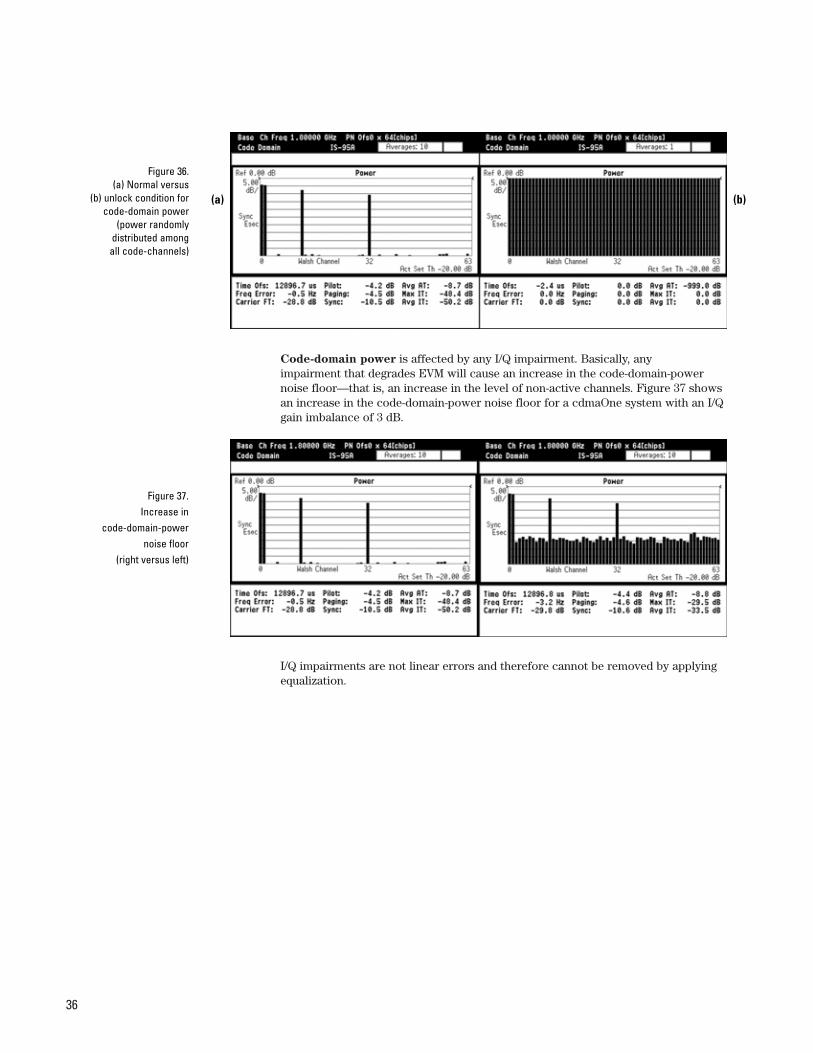
I/Q swapped results in an inverted spectrum. However, because of the noise-like shape of digitally-modulated signals, the inversion is usually undetectable inthe frequency domain. In the modulation domain, the data mapping is inverted,as seen in Figure 35, but the error cannot be detected, unless a known sequenceis measured. In CDMA signals, I/Q swapping errors can be detected by lookingat the code-domain power display. Since these errors result in an incorrecttransmitted symbol sequence, the measuring instrument can no longer find cor-relation to the codes. This causes an unlock condition, in which the correlatedpower is randomly distributed among all code-channels, as shown in Figure 36.Some vector signal analyzers have an inverted frequency mode that accounts forthis error and allows you verify it.
36
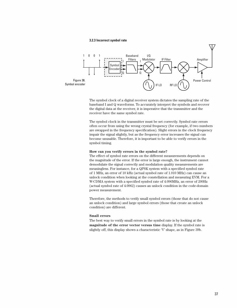
Code-domain power is affected by any I/Q impairment. Basically, any impairment that degrades EVM will cause an increase in the code-domain-powernoise floor—that is, an increase in the level of non-active channels. Figure 37 showsan increase in the code-domain-power noise floor for a cdmaOne system with an I/Qgain imbalance of 3 dB.
I/Q impairments are not linear errors and therefore cannot be removed by applyingequalization.
Figure 36. (a) Normal versus
(b) unlock condition forcode-domain power
(power randomly distributed among
all code-channels)
Figure 37. Increase in
code-domain-power noise floor
(right versus left)
(a) (b)
37
3.2.3 Incorrect symbol rate
The symbol clock of a digital receiver system dictates the sampling rate of thebaseband I and Q waveforms. To accurately interpret the symbols and recoverthe digital data at the receiver, it is imperative that the transmitter and thereceiver have the same symbol rate.
The symbol clock in the transmitter must be set correctly. Symbol rate errorsoften occur from using the wrong crystal frequency (for example, if two numbersare swapped in the frequency specification). Slight errors in the clock frequencyimpair the signal slightly, but as the frequency error increases the signal canbecome unusable. Therefore, it is important to be able to verify errors in thesymbol timing.
How can you verify errors in the symbol rate?
The effect of symbol rate errors on the different measurements depends on the magnitude of the error. If the error is large enough, the instrument cannotdemodulate the signal correctly and modulation quality measurements aremeaningless. For instance, for a QPSK system with a specified symbol rate of 1 MHz, an error of 10 kHz (actual symbol rate of 1.010 MHz) can cause anunlock condition when looking at the constellation and measuring EVM. For aW-CDMA system with a specified symbol rate of 4.096MHz, an error of 200Hz(actual symbol rate of 4.0962) causes an unlock condition in the code-domainpower measurement.
Therefore, the methods to verify small symbol errors (those that do not causean unlock condition) and large symbol errors (those that create an unlock condition) are different.
Small errors
The best way to verify small errors in the symbol rate is by looking at the magnitude of the error vector versus time display. If the symbol rate is slightly off, this display shows a characteristic ‘V’ shape, as in Figure 39b.
SymbolEncoder
RF LO
BasebandFilters IF FilterI
Q
I/QModulator
IF LO
I
Q
Amplifier
Power Control
1 0 0 1
Figure 38. Symbol encoder
38
This effect can be understood by studying Figure 40. For simplicity, a sinewaveis used instead of a digitally-modulated signal, and its frequency (symbol rate) isslightly higher than the specified sample frequency (symbol rate chosen in themeasuring instrument). At one arbitrary reference sample (called 0) the signalwill be sampled correctly. Since the symbol rate is slightly off, any other samplein the positive or negative direction will be slightly off in time. Therefore, thesignal will deviate by some amount from the perfect reference signal. This deviation or error vector grows linearly (on average) in both the positive andnegative directions. Therefore, the magnitude of the error vector versus timeshows a characteristic ‘V’ shape.
The smaller the symbol rate error, the more symbols are required to detect theerror (that is, to form the ‘V’ shape). For instance, in Figure 39b, for a QPSK system with a symbol rate specified at 1MHz, 100 symbols are measured to forma “V” shape in the magnitude of the error vector versus time display for an actualsymbol rate of 1.0025 MHz. In the same case, about 500 symbols are required toform a similar ‘V’ shape for an actual symbol rate of 1.00025 MHz.
Figure 39. (a) Constellation and
(b) magnitude of the errorvector versus time with
‘V’ shape caused byincorrect symbol rate
Actual Symbol Period
Sample Period
-2 -1 0 1 2
Error 1 or -1
Error 2 or -2
-2 -1 0 1 2
210
Graph of Error at Each Sample
Figure 40. Symbol rate slightly
higher than specified
39
The actual transmitted symbol rate can be found by adjusting the symbol rate inthe measuring instrument by trial and error until magnitude of the error vectorversus time looks flat.
Small symbol errors also affect the code-domain power measurement. The code-domain power noise floor increases proportionally to the magnitudeof the error.
Large errors
The best way to verify large symbol rate errors that produce unlock conditionsin the measurements is by measuring the signal’s channel bandwidth to roughlyapproximate the symbol rate, as explained in section 2.3.1.1.
Errors in the symbol rate are not linear and cannot be minimized by applyingequalization.
3.2.4 Wrong filter coefficients and incorrect windowing
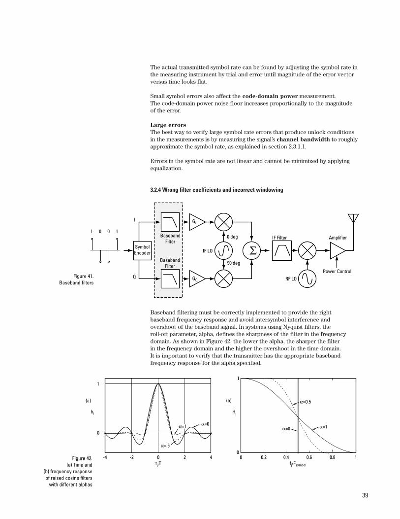
Baseband filtering must be correctly implemented to provide the right baseband frequency response and avoid intersymbol interference and overshoot of the baseband signal. In systems using Nyquist filters, the roll-off parameter, alpha, defines the sharpness of the filter in the frequencydomain. As shown in Figure 42, the lower the alpha, the sharper the filter in the frequency domain and the higher the overshoot in the time domain. It is important to verify that the transmitter has the appropriate basebandfrequency response for the alpha specified.
SymbolEncoder
RF LO
IF Filter
I
Q
BasebandFilter
BasebandFilter
IF LO
0 deg
90 deg
GQ
GI
1 0 0 1
ΣAmplifier
Power ControlFigure 41.
Baseband filters
-4 0 0.20 0.4 0.6 0.8fj/Fsymbol
Hj
ti/T
0
1
hi
α=.5
α=0 α=1
α=0.5(a) (b)
-2 2 4
α=1 α=0
10
1
Figure 42. (a) Time and
(b) frequency response of raised cosine filters
with different alphas
40
In many communications systems using Nyquist baseband filtering, the filterresponse is shared between the transmitter and the receiver. The filters must becompatible and correctly implemented in each. The type of filter and the roll-offfactor (alpha) are the key parameters that must be considered.
The main causes of error in baseband filtering are the following:
1. Wrong filter coefficients. For Nyquist filters, an error in the implementationof alpha may result in undesirable amplitude overshoot in the signal or interferencein the adjacent frequency channel. It may also degrade intersymbol interference(ISI) caused by fading.
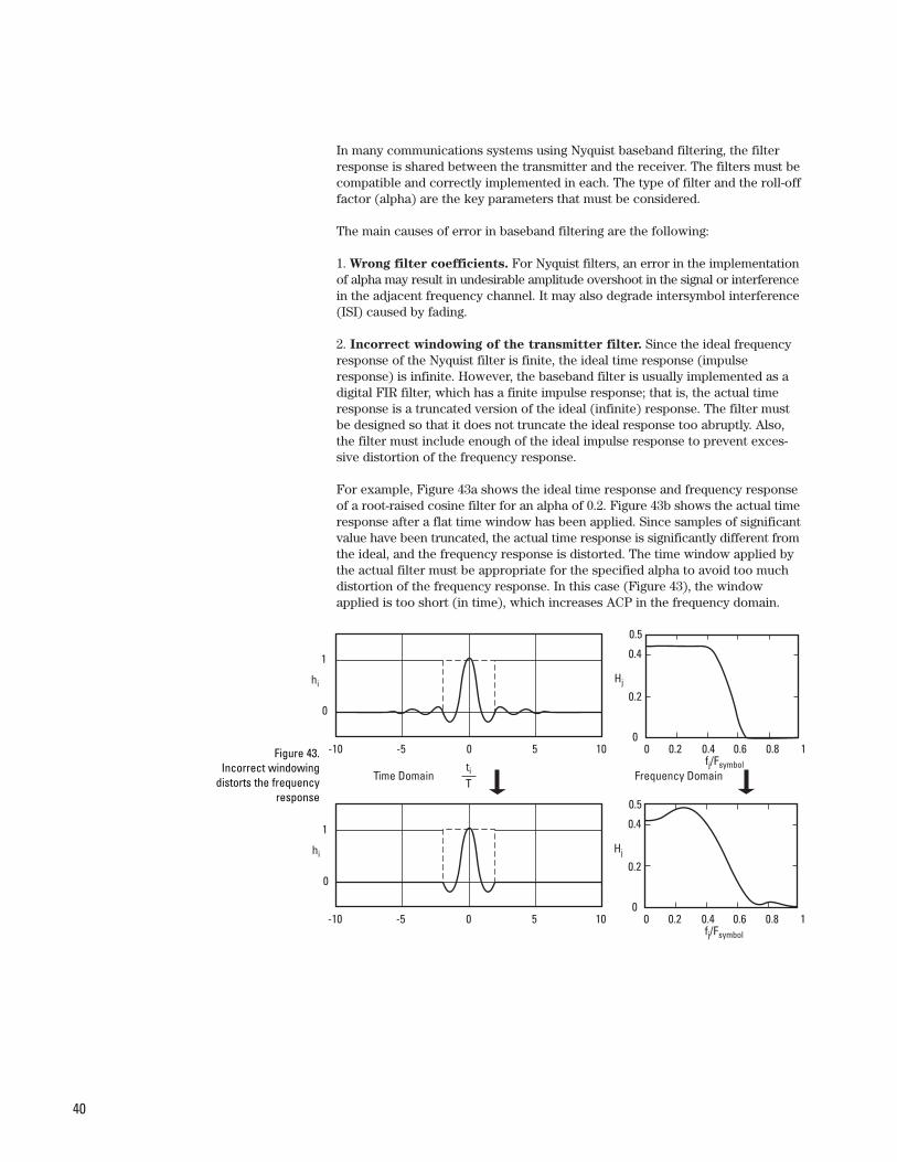
2. Incorrect windowing of the transmitter filter. Since the ideal frequencyresponse of the Nyquist filter is finite, the ideal time response (impulseresponse) is infinite. However, the baseband filter is usually implemented as adigital FIR filter, which has a finite impulse response; that is, the actual timeresponse is a truncated version of the ideal (infinite) response. The filter mustbe designed so that it does not truncate the ideal response too abruptly. Also,the filter must include enough of the ideal impulse response to prevent exces-sive distortion of the frequency response.
For example, Figure 43a shows the ideal time response and frequency responseof a root-raised cosine filter for an alpha of 0.2. Figure 43b shows the actual timeresponse after a flat time window has been applied. Since samples of significantvalue have been truncated, the actual time response is significantly different fromthe ideal, and the frequency response is distorted. The time window applied bythe actual filter must be appropriate for the specified alpha to avoid too muchdistortion of the frequency response. In this case (Figure 43), the windowapplied is too short (in time), which increases ACP in the frequency domain.
-10 -5 0 5 10 0 0.2 0.4 0.6 0.8 1
0.5
0.2
0
0.4
fj/Fsymbol
Hj
Time Domain Frequency Domain
-10 -5 0 5 10 0 0.2 0.4 0.6 0.8 1
0.5
0.2
0
0.4
fj/Fsymbol
Hj
ti
T
hi
0
1
hi
0
1
Figure 43. Incorrect windowing
distorts the frequencyresponse
41
How can you verify errors in the alpha coefficient and the windowing?
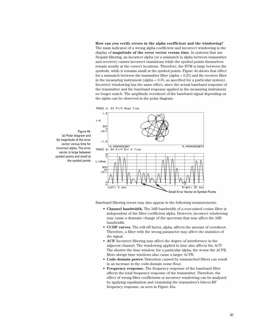
The main indicator of a wrong alpha coefficient and incorrect windowing is thedisplay of magnitude of the error vector versus time. In systems that useNyquist filtering, an incorrect alpha (or a mismatch in alpha between transmitterand receiver) causes incorrect transitions while the symbol points themselvesremain mostly at the correct locations. Therefore, the EVM is large between thesymbols, while it remains small at the symbol points. Figure 44 shows that effectfor a mismatch between the transmitter filter (alpha = 0.25) and the receiver filterin the measuring instrument (alpha = 0.35, as specified for a particular system).Incorrect windowing has the same effect, since the actual baseband response ofthe transmitter and the baseband response applied in the measuring instrumentno longer match. The amplitude overshoot of the baseband signal depending onthe alpha can be observed in the polar diagram.
Baseband filtering errors may also appear in the following measurements:
• Channel bandwidth. The 3dB bandwidth of a root-raised cosine filter is independent of the filter coefficient alpha. However, incorrect windowingmay cause a dramatic change of the spectrum that may affect the 3dB bandwidth.
• CCDF curves. The roll-off factor, alpha, affects the amount of overshoot.Therefore, a filter with the wrong parameter may affect the statistics of the signal.
• ACP. Incorrect filtering may affect the degree of interference in theadjacent channel. The windowing applied in time also affects the ACP. The shorter the time window, for a particular alpha, the worse the ACPR.More abrupt time windows also cause a larger ACPR.
• Code-domain power. Distortion caused by mismatched filters can resultin an increase in the code-domain noise floor.
• Frequency response. The frequency response of the baseband filter affects the total frequency response of the transmitter. Therefore, the effect of wrong filter coefficients or incorrect windowing can be analyzedby applying equalization and examining the transmitter’s bits-to-RF frequency response, as seen in Figure 45a.
Figure 44. (a) Polar diagram and
(b) magnitude of the errorvector versus time for
incorrect alpha. The error vector is large between
symbol points and small atthe symbol points
Small Error Vector at Symbol Points
42
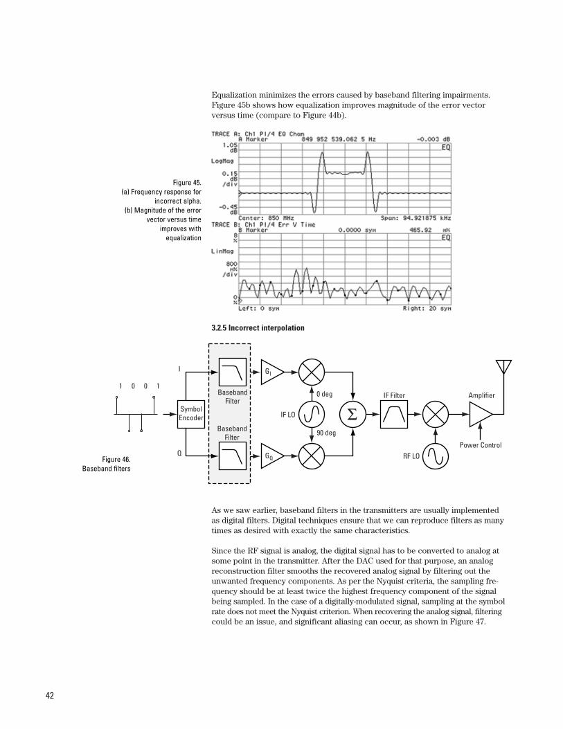
Equalization minimizes the errors caused by baseband filtering impairments.Figure 45b shows how equalization improves magnitude of the error vector versus time (compare to Figure 44b).
3.2.5 Incorrect interpolation
As we saw earlier, baseband filters in the transmitters are usually implementedas digital filters. Digital techniques ensure that we can reproduce filters as manytimes as desired with exactly the same characteristics.
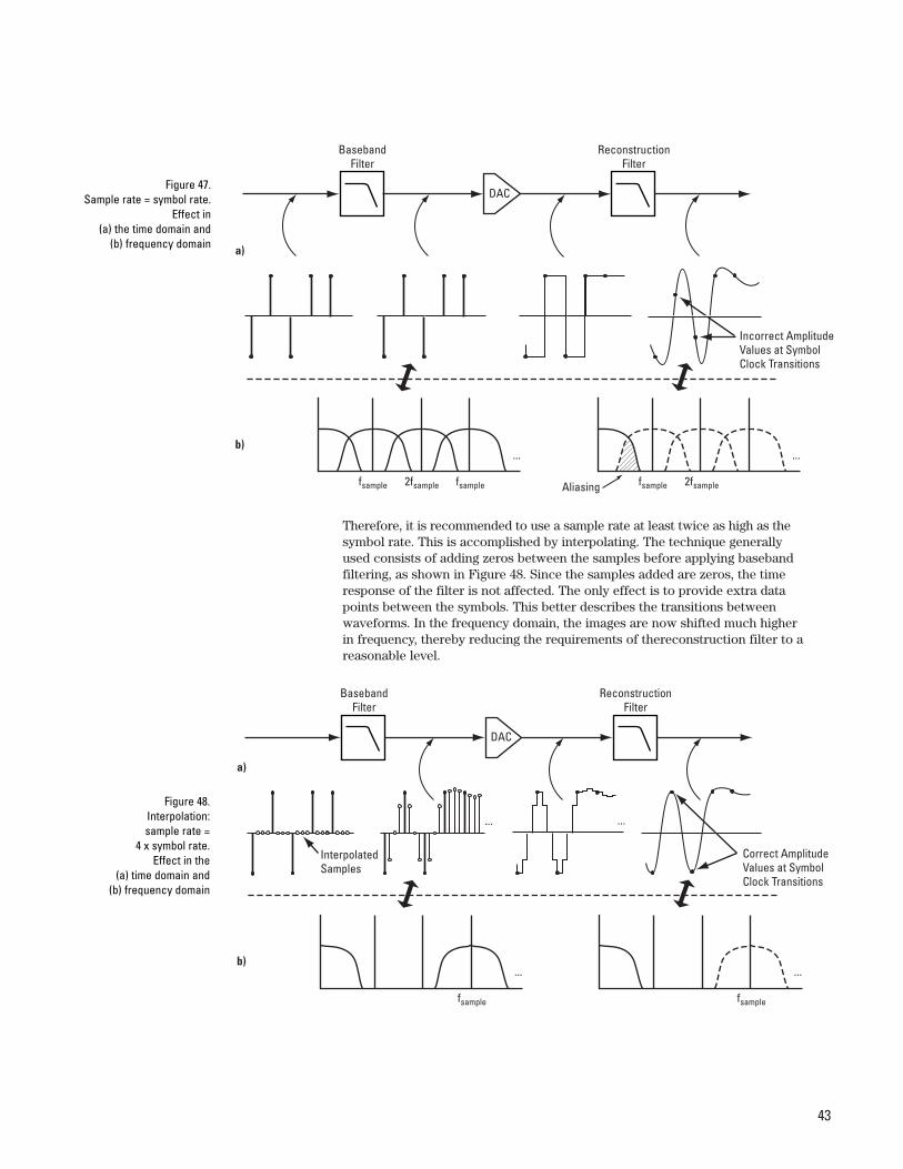
Since the RF signal is analog, the digital signal has to be converted to analog atsome point in the transmitter. After the DAC used for that purpose, an analogreconstruction filter smooths the recovered analog signal by filtering out theunwanted frequency components. As per the Nyquist criteria, the sampling fre-quency should be at least twice the highest frequency component of the signalbeing sampled. In the case of a digitally-modulated signal, sampling at the symbolrate does not meet the Nyquist criterion. When recovering the analog signal, filteringcould be an issue, and significant aliasing can occur, as shown in Figure 47.
Figure 45. (a) Frequency response for
incorrect alpha.(b) Magnitude of the error
vector versus timeimproves with
equalization
SymbolEncoder
RF LO
IF Filter
I
Q
BasebandFilter
BasebandFilter
IF LO
0 deg
90 deg
GQ
GI
ΣAmplifier
Power Control
1 0 0 1
Figure 46. Baseband filters
43
Therefore, it is recommended to use a sample rate at least twice as high as thesymbol rate. This is accomplished by interpolating. The technique generallyused consists of adding zeros between the samples before applying basebandfiltering, as shown in Figure 48. Since the samples added are zeros, the timeresponse of the filter is not affected. The only effect is to provide extra datapoints between the symbols. This better describes the transitions betweenwaveforms. In the frequency domain, the images are now shifted much higherin frequency, thereby reducing the requirements of thereconstruction filter to areasonable level.
...
Incorrect AmplitudeValues at SymbolClock Transitions
BasebandFilter
DAC
ReconstructionFilter
a)
b)
fsample
...
fsample 2fsample fsample 2fsampleAliasing
Figure 47. Sample rate = symbol rate.
Effect in (a) the time domain and
(b) frequency domain
...
Correct AmplitudeValues at SymbolClock Transitions
BasebandFilter
DAC
ReconstructionFilter
a)
b)
fsample
...
fsample
...
InterpolatedSamples
...
Figure 48. Interpolation: sample rate =
4 x symbol rate. Effect in the
(a) time domain and (b) frequency domain
44
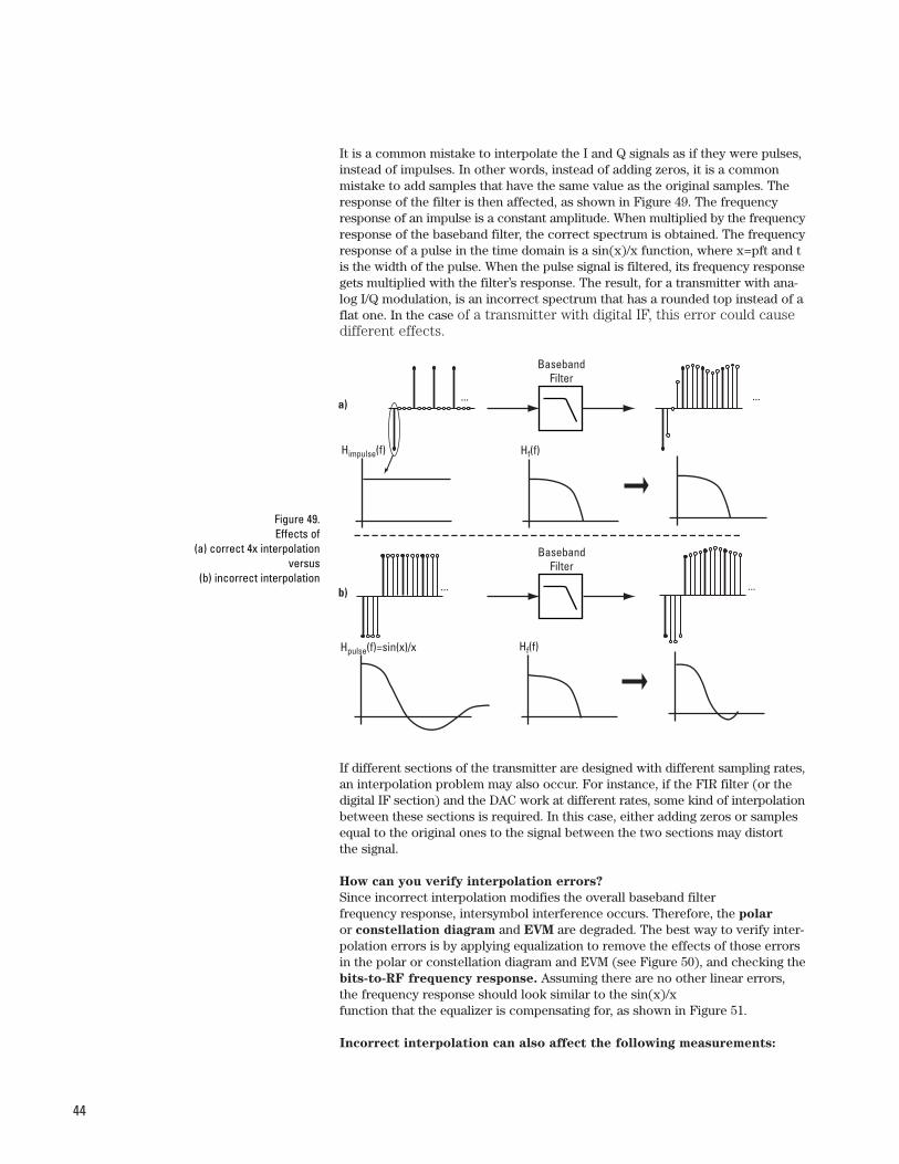
It is a common mistake to interpolate the I and Q signals as if they were pulses,instead of impulses. In other words, instead of adding zeros, it is a commonmistake to add samples that have the same value as the original samples. Theresponse of the filter is then affected, as shown in Figure 49. The frequencyresponse of an impulse is a constant amplitude. When multiplied by the frequencyresponse of the baseband filter, the correct spectrum is obtained. The frequencyresponse of a pulse in the time domain is a sin(x)/x function, where x=pft and tis the width of the pulse. When the pulse signal is filtered, its frequency responsegets multiplied with the filter’s response. The result, for a transmitter with ana-log I/Q modulation, is an incorrect spectrum that has a rounded top instead of aflat one. In the case of a transmitter with digital IF, this error could causedifferent effects.
If different sections of the transmitter are designed with different sampling rates,an interpolation problem may also occur. For instance, if the FIR filter (or thedigital IF section) and the DAC work at different rates, some kind of interpolationbetween these sections is required. In this case, either adding zeros or samplesequal to the original ones to the signal between the two sections may distort the signal.
How can you verify interpolation errors?
Since incorrect interpolation modifies the overall baseband filter frequency response, intersymbol interference occurs. Therefore, the polar
or constellation diagram and EVM are degraded. The best way to verify inter-polation errors is by applying equalization to remove the effects of those errorsin the polar or constellation diagram and EVM (see Figure 50), and checking thebits-to-RF frequency response. Assuming there are no other linear errors,the frequency response should look similar to the sin(x)/x function that the equalizer is compensating for, as shown in Figure 51.
Incorrect interpolation can also affect the following measurements:
BasebandFilter
a)
b)
...
Himpulse(f) Hf(f)
Hf(f)Hpulse(f)=sin(x)/x
BasebandFilter
... ...
...
Figure 49. Effects of
(a) correct 4x interpolation versus
(b) incorrect interpolation

45
• Channel bandwidth. Incorrect interpolation has an impact on the spectrumshape. For instance, for a transmitter with analog I/Q, the spectrum of a signal with incorrect interpolation has a rounded top instead of a flat one.Therefore, the channel bandwidth measurement may be affected. For example, Figure 52 shows a 3 dB bandwidth of 665 kHz for a signal with asymbol rate of 1 MHz.
Figure 50. Effect of equalization on sig-
nal with incorrect interpolation: polar
diagram and magnitude of the error vec-
tor versus time (a) without
equalization and (b) with equalization
Figure 51. Bits-to-RF frequency response of
transmitter with incorrect interpolation
(a) (b)
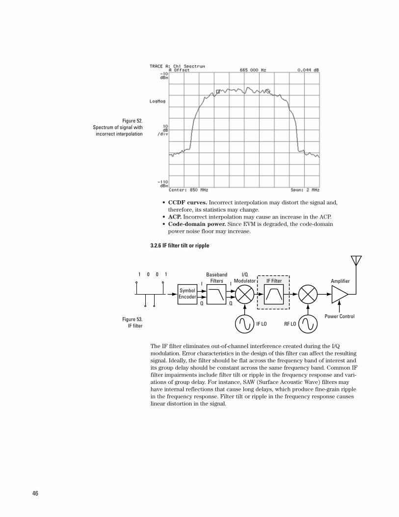
46
• CCDF curves. Incorrect interpolation may distort the signal and, therefore, its statistics may change.
• ACP. Incorrect interpolation may cause an increase in the ACP.• Code-domain power. Since EVM is degraded, the code-domain
power noise floor may increase.
3.2.6 IF filter tilt or ripple
The IF filter eliminates out-of-channel interference created during the I/Q modulation. Error characteristics in the design of this filter can affect the resultingsignal. Ideally, the filter should be flat across the frequency band of interest andits group delay should be constant across the same frequency band. Common IFfilter impairments include filter tilt or ripple in the frequency response and vari-ations of group delay. For instance, SAW (Surface Acoustic Wave) filters mayhave internal reflections that cause long delays, which produce fine-grain ripplein the frequency response. Filter tilt or ripple in the frequency response causeslinear distortion in the signal.
Figure 52. Spectrum of signal with
incorrect interpolation
SymbolEncoder
RF LO
BasebandFilters IF FilterI
Q
I/QModulator
IF LO
I
Q
Amplifier
Power Control
1 0 0 1
Figure 53. IF filter
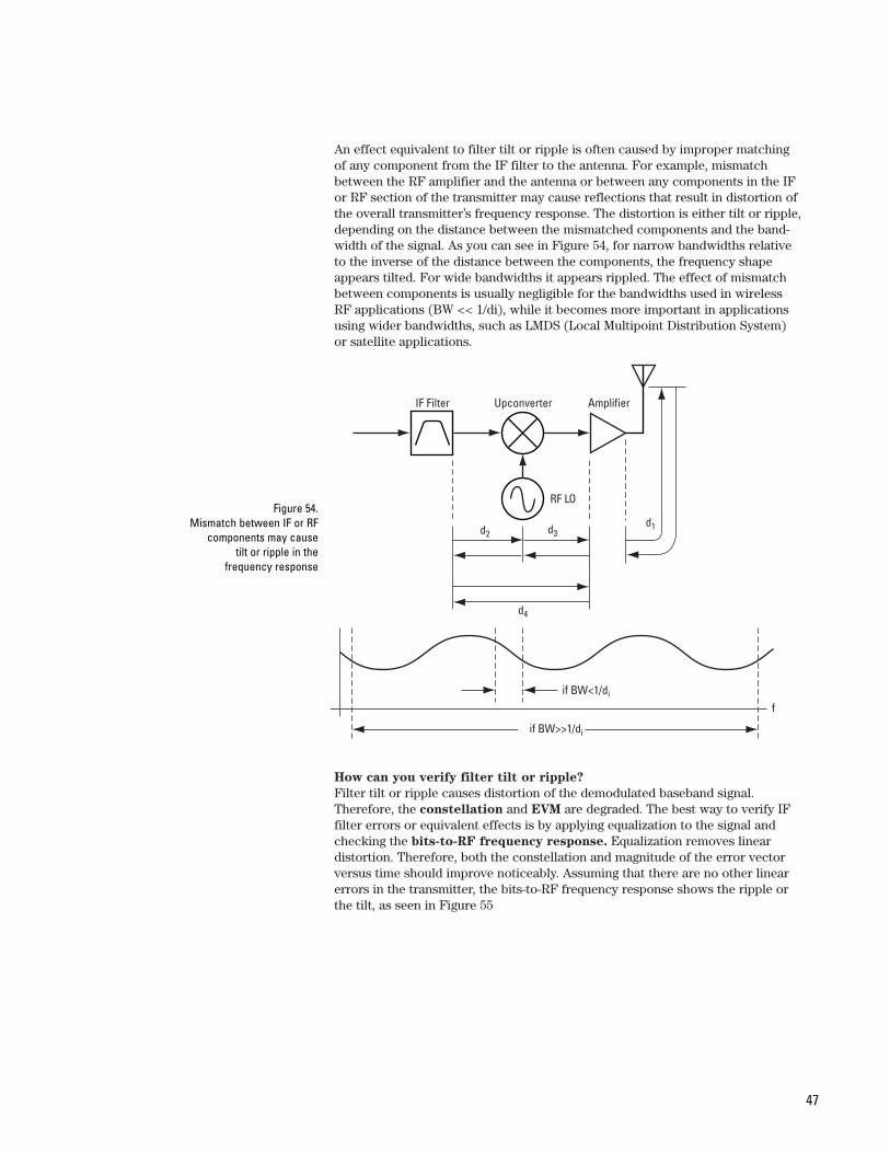
47
An effect equivalent to filter tilt or ripple is often caused by improper matchingof any component from the IF filter to the antenna. For example, mismatchbetween the RF amplifier and the antenna or between any components in the IFor RF section of the transmitter may cause reflections that result in distortion ofthe overall transmitter’s frequency response. The distortion is either tilt or ripple,depending on the distance between the mismatched components and the band-width of the signal. As you can see in Figure 54, for narrow bandwidths relativeto the inverse of the distance between the components, the frequency shapeappears tilted. For wide bandwidths it appears rippled. The effect of mismatchbetween components is usually negligible for the bandwidths used in wirelessRF applications (BW << 1/di), while it becomes more important in applicationsusing wider bandwidths, such as LMDS (Local Multipoint Distribution System)or satellite applications.
How can you verify filter tilt or ripple?
Filter tilt or ripple causes distortion of the demodulated baseband signal.Therefore, the constellation and EVM are degraded. The best way to verify IFfilter errors or equivalent effects is by applying equalization to the signal andchecking the bits-to-RF frequency response. Equalization removes linear distortion. Therefore, both the constellation and magnitude of the error vectorversus time should improve noticeably. Assuming that there are no other linearerrors in the transmitter, the bits-to-RF frequency response shows the ripple orthe tilt, as seen in Figure 55
Amplifier
RF LO
UpconverterIF Filter
d2 d3
d4
if BW<1/di
if BW>>1/di
d1
f
Figure 54. Mismatch between IF or RF
components may cause tilt or ripple in the
frequency response
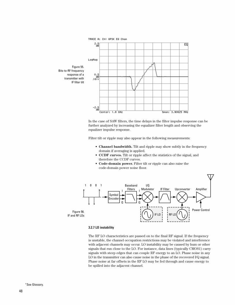
48
In the case of SAW filters, the time delays in the filter impulse response can befurther analyzed by increasing the equalizer filter length and observing theequalizer impulse response.
Filter tilt or ripple may also appear in the following measurements:
• Channel bandwidth. Tilt and ripple may show subtly in the frequency domain if averaging is applied.
• CCDF curves. Tilt or ripple affect the statistics of the signal, and therefore the CCDF curves.
• Code-domain power. Filter tilt or ripple can also raise the code-domain power noise floor.
3.2.7 LO instability
The RF LO characteristics are passed on to the final RF signal. If the frequencyis unstable, the channel occupation restrictions may be violated and interferencewith adjacent channels may occur. LO instability may be caused by hum or othersignals that run close to the LO. For instance, data lines (typically CMOS1) carrysignals with steep edges that can couple RF energy to an LO. Phase noise in anyLO in the transmitter can also cause noise in the phase of the recovered I/Q signal.Phase noise at far offsets in the RF LO may be fed through and cause energy tobe spilled into the adjacent channel.
Figure 55. Bits-to-RF frequency
response of a transmitter with
IF filter tilt
SymbolEncoder
RF LO
BasebandFilters IF FilterI
Q
I/QModulator
IF LO
I
Q
Upconverter Amplifier
Power Control
1 0 0 1
Figure 56. IF and RF LOs
1 See Glossary.
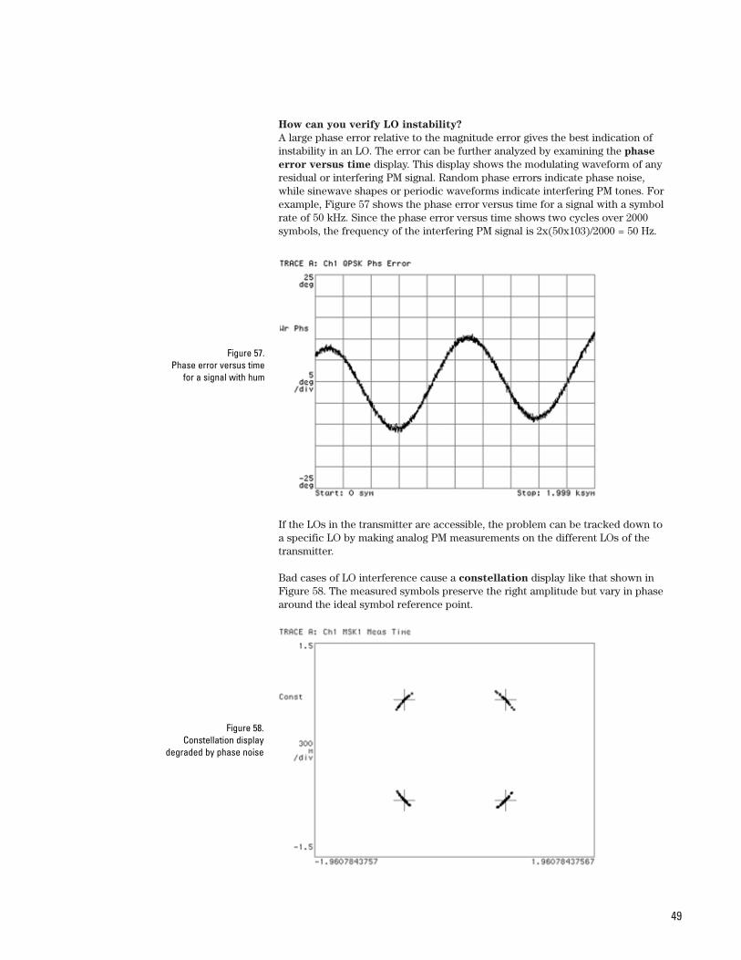
49
How can you verify LO instability?
A large phase error relative to the magnitude error gives the best indication ofinstability in an LO. The error can be further analyzed by examining the phase
error versus time display. This display shows the modulating waveform of anyresidual or interfering PM signal. Random phase errors indicate phase noise,while sinewave shapes or periodic waveforms indicate interfering PM tones. Forexample, Figure 57 shows the phase error versus time for a signal with a symbolrate of 50 kHz. Since the phase error versus time shows two cycles over 2000symbols, the frequency of the interfering PM signal is 2x(50x103)/2000 = 50 Hz.
If the LOs in the transmitter are accessible, the problem can be tracked down toa specific LO by making analog PM measurements on the different LOs of thetransmitter.
Bad cases of LO interference cause a constellation display like that shown inFigure 58. The measured symbols preserve the right amplitude but vary in phasearound the ideal symbol reference point.
Figure 57. Phase error versus time
for a signal with hum
Figure 58. Constellation display
degraded by phase noise
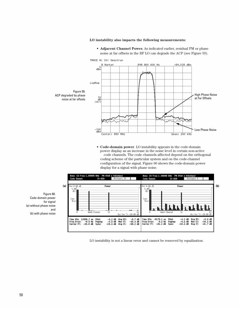
50
LO instability also impacts the following measurements:
• Adjacent Channel Power. As indicated earlier, residual PM or phase noise at far offsets in the RF LO can degrade the ACP (see Figure 59).
• Code-domain power. LO instability appears in the code-domain power display as an increase in the noise level in certain non-active
code channels. The code channels affected depend on the orthogonal coding scheme of the particular system and on the code-channel configuration of the signal. Figure 60 shows the code-domain power display for a signal with phase noise.
LO instability is not a linear error and cannot be removed by equalization.
Figure 59.ACP degraded by phase
noise at far offsets
Figure 60. Code-domain power
for signal (a) without phase noise
and (b) with phase noise
High Phase Noise at Far Offsets
Low Phase Noise
(a) (b)
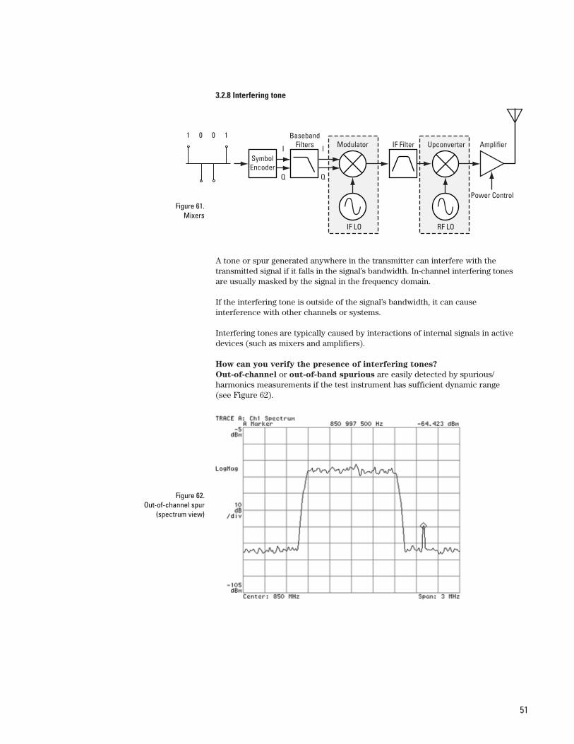
51
3.2.8 Interfering tone
A tone or spur generated anywhere in the transmitter can interfere with thetransmitted signal if it falls in the signal’s bandwidth. In-channel interfering tonesare usually masked by the signal in the frequency domain.
If the interfering tone is outside of the signal’s bandwidth, it can cause interference with other channels or systems.
Interfering tones are typically caused by interactions of internal signals in activedevices (such as mixers and amplifiers).
How can you verify the presence of interfering tones?
Out-of-channel or out-of-band spurious are easily detected by spurious/harmonics measurements if the test instrument has sufficient dynamic range(see Figure 62).
SymbolEncoder
RF LO
BasebandFilters IF FilterI
Q
Modulator
IF LO
I
Q
Upconverter1 0 0 1
Amplifier
Power ControlFigure 61.
Mixers
Figure 62. Out-of-channel spur
(spectrum view)
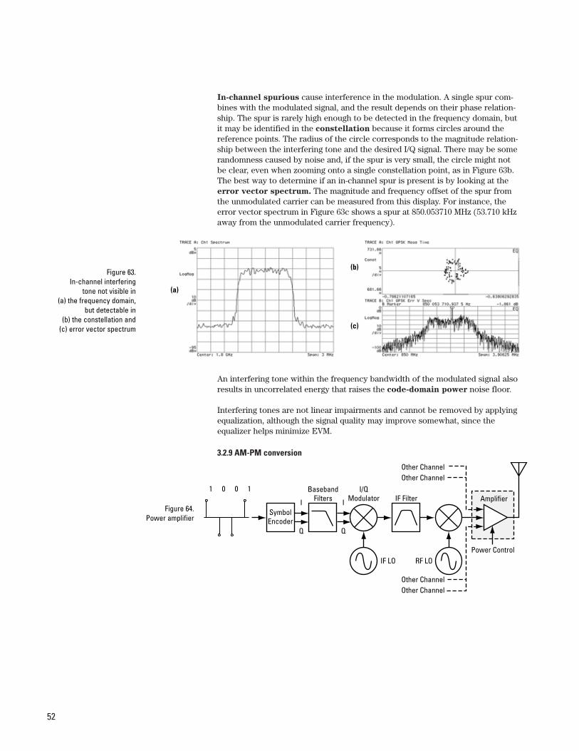
52
In-channel spurious cause interference in the modulation. A single spur com-bines with the modulated signal, and the result depends on their phase relation-ship. The spur is rarely high enough to be detected in the frequency domain, butit may be identified in the constellation because it forms circles around thereference points. The radius of the circle corresponds to the magnitude relation-ship between the interfering tone and the desired I/Q signal. There may be somerandomness caused by noise and, if the spur is very small, the circle might notbe clear, even when zooming onto a single constellation point, as in Figure 63b.The best way to determine if an in-channel spur is present is by looking at theerror vector spectrum. The magnitude and frequency offset of the spur fromthe unmodulated carrier can be measured from this display. For instance, theerror vector spectrum in Figure 63c shows a spur at 850.053710 MHz (53.710 kHzaway from the unmodulated carrier frequency).
An interfering tone within the frequency bandwidth of the modulated signal alsoresults in uncorrelated energy that raises the code-domain power noise floor.
Interfering tones are not linear impairments and cannot be removed by applyingequalization, although the signal quality may improve somewhat, since theequalizer helps minimize EVM.
3.2.9 AM-PM conversion
Figure 63. In-channel interfering
tone not visible in (a) the frequency domain,
but detectable in (b) the constellation and
(c) error vector spectrum
SymbolEncoder
RF LO
BasebandFilters IF FilterI
Q
I/QModulator
IF LO
I
Q
Other ChannelOther Channel
Other ChannelOther Channel
Amplifier
Power Control
1 0 0 1
Figure 64. Power amplifier
(a)
(b)
(c)
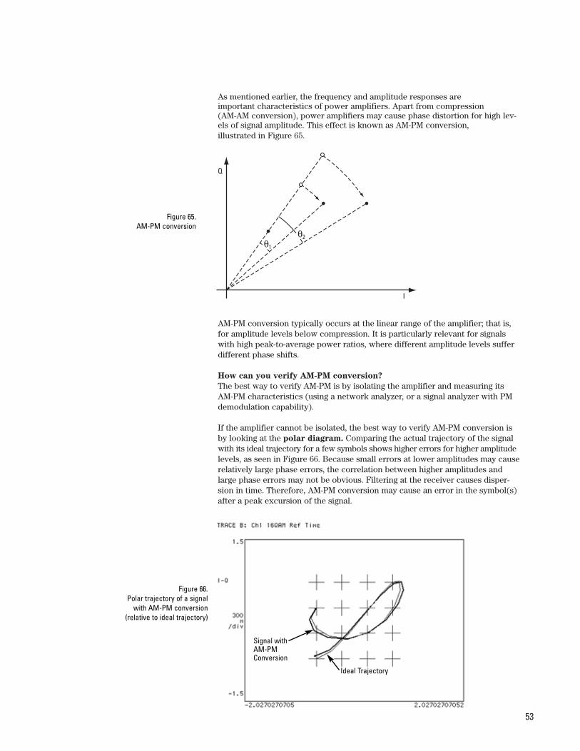
53
As mentioned earlier, the frequency and amplitude responses areimportant characteristics of power amplifiers. Apart from compression (AM-AM conversion), power amplifiers may cause phase distortion for high lev-els of signal amplitude. This effect is known as AM-PM conversion, illustrated in Figure 65.
AM-PM conversion typically occurs at the linear range of the amplifier; that is,for amplitude levels below compression. It is particularly relevant for signalswith high peak-to-average power ratios, where different amplitude levels sufferdifferent phase shifts.
How can you verify AM-PM conversion?
The best way to verify AM-PM is by isolating the amplifier and measuring itsAM-PM characteristics (using a network analyzer, or a signal analyzer with PMdemodulation capability).
If the amplifier cannot be isolated, the best way to verify AM-PM conversion isby looking at the polar diagram. Comparing the actual trajectory of the signalwith its ideal trajectory for a few symbols shows higher errors for higher amplitudelevels, as seen in Figure 66. Because small errors at lower amplitudes may causerelatively large phase errors, the correlation between higher amplitudes andlarge phase errors may not be obvious. Filtering at the receiver causes disper-sion in time. Therefore, AM-PM conversion may cause an error in the symbol(s)after a peak excursion of the signal.
Q
I
θ2θ1
Figure 65. AM-PM conversion
Figure 66. Polar trajectory of a signal
with AM-PM conversion(relative to ideal trajectory)
Signal withAM-PMConversion
Ideal Trajectory
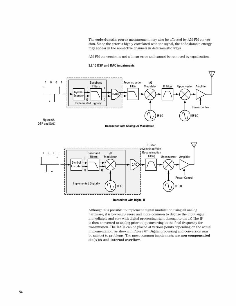
54
The code-domain power measurement may also be affected by AM-PM conver-sion. Since the error is highly correlated with the signal, the code-domain energymay appear in the non-active channels in deterministic ways.
AM-PM conversion is not a linear error and cannot be removed by equalization.
3.2.10 DSP and DAC impairments
Although it is possible to implement digital modulation using all analog hardware, it is becoming more and more common to digitize the input signalimmediately and stay with digital processing right through to the IF. The IF is then converted to analog prior to upconverting to the final frequency fortransmission. The DACs can be placed at various points depending on the actualimplementation, as shown in Figure 67. Digital processing and conversion maybe subject to problems. The most common impairments are non-compensated
sin(x)/x and internal overflow.
SymbolEncoder
RF LO
UpconverterBaseband
Filters
IF Filter(Combined With Reconstruction
Filter)I
Q
I/QModulator
IF LO
DAC
I
Q
Implemented Digitally
SymbolEncoder
RF LO
UpconverterBaseband
Filters IF FilterI
Q
I/QModulator
IF LO
DACs
I
QImplemented Digitally
Reconstruction Filter Amplifier
Power Control
Transmitter with Analog I/Q Modulation
Transmitter with Digital IF
Amplifier
Power Control
1 0 0 1
1 0 0 1
Figure 67. DSP and DAC
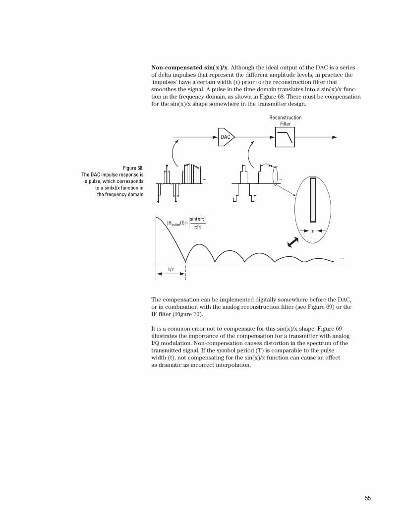
55
Non-compensated sin(x)/x. Although the ideal output of the DAC is a series of delta impulses that represent the different amplitude levels, in practice the‘impulses’ have a certain width (t) prior to the reconstruction filter thatsmoothes the signal. A pulse in the time domain translates into a sin(x)/x func-tion in the frequency domain, as shown in Figure 68. There must be compensationfor the sin(x)/x shape somewhere in the transmitter design.
The compensation can be implemented digitally somewhere before the DAC, or in combination with the analog reconstruction filter (see Figure 69) or the IF filter (Figure 70).
It is a common error not to compensate for this sin(x)/x shape. Figure 69 illustrates the importance of the compensation for a transmitter with analog I/Q modulation. Non-compensation causes distortion in the spectrum of thetransmitted signal. If the symbol period (T) is comparable to the pulse width (t), not compensating for the sin(x)/x function can cause an effect as dramatic as incorrect interpolation.
DAC
ReconstructionFilter
...
1/τ
τ
... ...
Figure 68. The DAC impulse response is
a pulse, which corresponds to a sin(x)/x function in the frequency domain
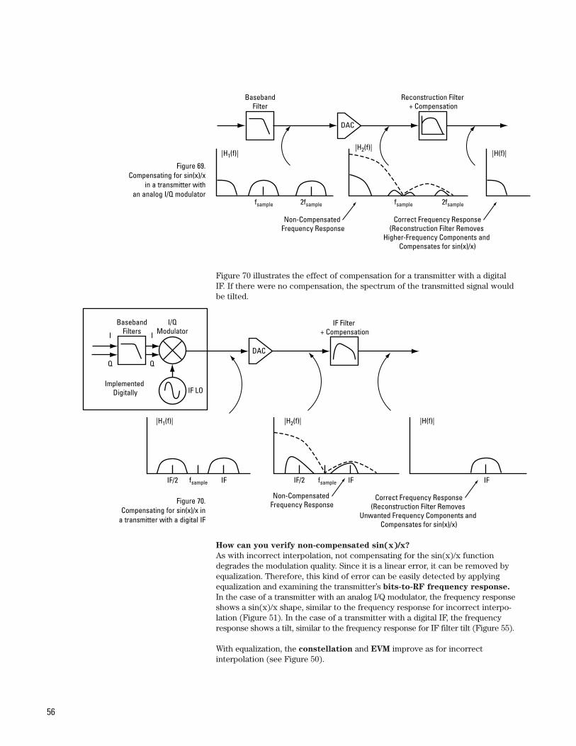
56
Figure 70 illustrates the effect of compensation for a transmitter with a digitalIF. If there were no compensation, the spectrum of the transmitted signal wouldbe tilted.
How can you verify non-compensated sin(x)/x?
As with incorrect interpolation, not compensating for the sin(x)/x functiondegrades the modulation quality. Since it is a linear error, it can be removed byequalization. Therefore, this kind of error can be easily detected by applyingequalization and examining the transmitter’s bits-to-RF frequency response.
In the case of a transmitter with an analog I/Q modulator, the frequency responseshows a sin(x)/x shape, similar to the frequency response for incorrect interpo-lation (Figure 51). In the case of a transmitter with a digital IF, the frequencyresponse shows a tilt, similar to the frequency response for IF filter tilt (Figure 55).
With equalization, the constellation and EVM improve as for incorrect interpolation (see Figure 50).
BasebandFilter
DAC
Reconstruction Filter + Compensation
fsample 2fsample fsample 2fsample
Correct Frequency Response(Reconstruction Filter Removes
Higher-Frequency Components and Compensates for sin(x)/x)
|H1(f)||H2(f)|
|H(f)|
Non-Compensated Frequency Response
Figure 69. Compensating for sin(x)/x
in a transmitter with an analog I/Q modulator
DAC
IF Filter + Compensation
fsample IF
Correct Frequency Response(Reconstruction Filter Removes
Unwanted Frequency Components and Compensates for sin(x)/x)
|H(f)|
Non-Compensated Frequency Response
IFIF/2
BasebandFiltersI
Q
I/QModulator
IF LO
I
Q
Implemented Digitally
fsample IFIF/2
|H2(f)||H1(f)|
Figure 70. Compensating for sin(x)/x in
a transmitter with a digital IF
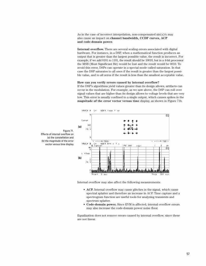
57
As in the case of incorrect interpolation, non-compensated sin(x)/x may also cause an impact on channel bandwidth, CCDF curves, ACP
and code-domain power.
Internal overflow. There are several scaling errors associated with digitalhardware. For instance, in a DSP, when a mathematical function produces anoutput that is greater than the largest possible value, the result is incorrect. Forexample, if we add 0101 to 1101, the result should be 10010, but in a 4-bit processorthe MSB (Most Significant Bit) would be lost and the result would be 0010. Toavoid this error, DSPs can operate in a special mode called saturation. In thatcase the DSP saturates to all ones if the result is greater than the largest possi-ble value, and to all zeros if the result is less than the smallest acceptable value.
How can you verify errors caused by internal overflow?
If the DSP’s algorithms yield values greater than its design allows, artifacts canoccur in the modulation. For example, as we saw above, the DSP can roll oversignal values that are higher than its design allows to voltage levels that are verylow. This error is usually confined to a single output, which causes spikes in themagnitude of the error vector versus time display, as shown in Figure 71b.
Internal overflow may also affect the following measurements:
• ACP. Internal overflow may cause glitches in the signal, which cause spectral splatter and therefore an increase in ACP. Time capture and a spectrogram function are useful tools for analyzing transients and spectrum splatter.
• Code-domain power. Since EVM is affected, internal overflow errors may also increase the code-domain power noise floor.
Equalization does not remove errors caused by internal overflow, since theseare not linear.
Figure 71. Effects of internal overflow on
(a) the constellation and (b) the magnitude of the error
vector versus time display
(b)
(a)
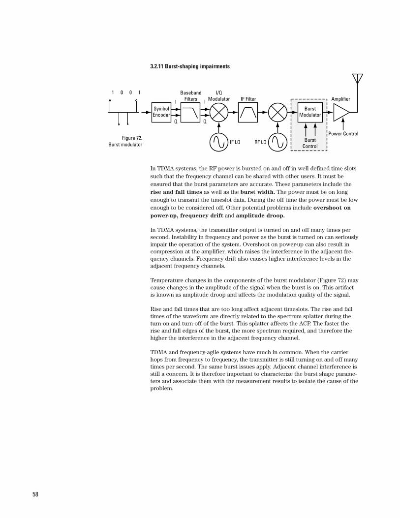
58
3.2.11 Burst-shaping impairments
In TDMA systems, the RF power is bursted on and off in well-defined time slotssuch that the frequency channel can be shared with other users. It must beensured that the burst parameters are accurate. These parameters include therise and fall times as well as the burst width. The power must be on longenough to transmit the timeslot data. During the off time the power must be lowenough to be considered off. Other potential problems include overshoot on
power-up, frequency drift and amplitude droop.
In TDMA systems, the transmitter output is turned on and off many times persecond. Instability in frequency and power as the burst is turned on can seriouslyimpair the operation of the system. Overshoot on power-up can also result incompression at the amplifier, which raises the interference in the adjacent fre-quency channels. Frequency drift also causes higher interference levels in theadjacent frequency channels.
Temperature changes in the components of the burst modulator (Figure 72) maycause changes in the amplitude of the signal when the burst is on. This artifactis known as amplitude droop and affects the modulation quality of the signal.
Rise and fall times that are too long affect adjacent timeslots. The rise and falltimes of the waveform are directly related to the spectrum splatter during theturn-on and turn-off of the burst. This splatter affects the ACP. The faster therise and fall edges of the burst, the more spectrum required, and therefore thehigher the interference in the adjacent frequency channel.
TDMA and frequency-agile systems have much in common. When the carrierhops from frequency to frequency, the transmitter is still turning on and off manytimes per second. The same burst issues apply. Adjacent channel interference isstill a concern. It is therefore important to characterize the burst shape parame-ters and associate them with the measurement results to isolate the cause of theproblem.
SymbolEncoder
RF LO
BasebandFilters IF FilterI
Q
I/QModulator
IF LO
I
Q
BurstModulator
BurstControl
Amplifier
Power Control
1 0 0 1
Figure 72. Burst modulator
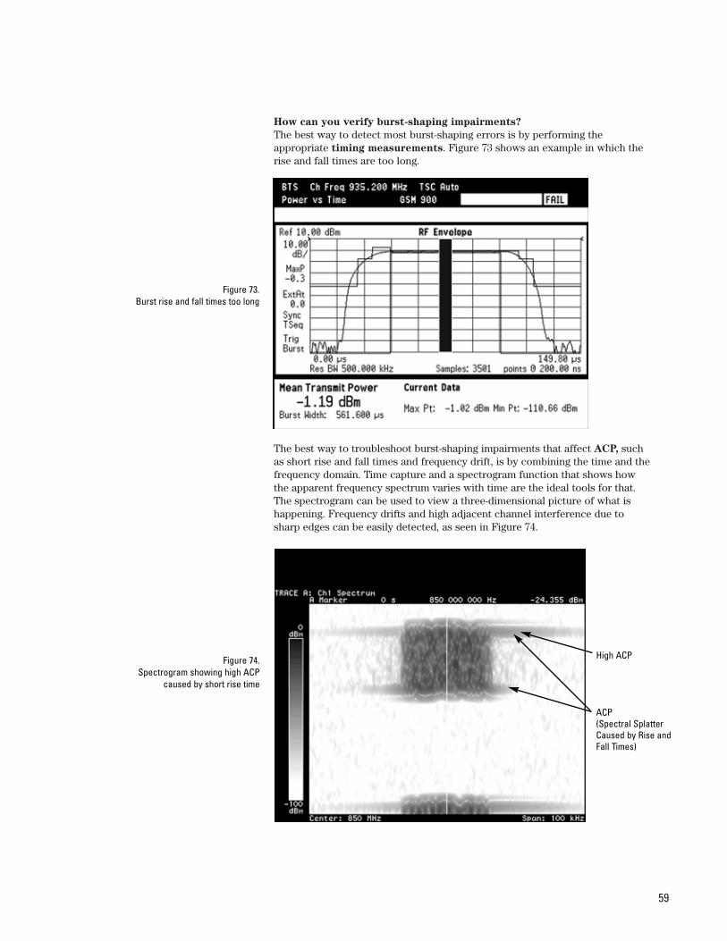
59
How can you verify burst-shaping impairments?
The best way to detect most burst-shaping errors is by performing the appropriate timing measurements. Figure 73 shows an example in which therise and fall times are too long.
The best way to troubleshoot burst-shaping impairments that affect ACP, suchas short rise and fall times and frequency drift, is by combining the time and thefrequency domain. Time capture and a spectrogram function that shows howthe apparent frequency spectrum varies with time are the ideal tools for that.The spectrogram can be used to view a three-dimensional picture of what ishappening. Frequency drifts and high adjacent channel interference due tosharp edges can be easily detected, as seen in Figure 74.
Figure 73. Burst rise and fall times too long
Figure 74. Spectrogram showing high ACP
caused by short rise time
High ACP
ACP(Spectral SplatterCaused by Rise and Fall Times)
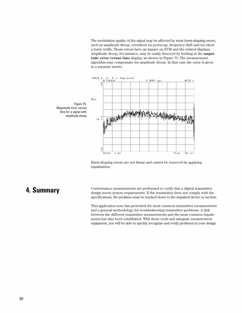
60
The modulation quality of the signal may be affected by most burst-shaping errors,such as amplitude droop, overshoot on power-up, frequency drift and too shorta burst width. Those errors have an impact on EVM and the related displays.Amplitude droop, for instance, may be easily detected by looking at the magni-
tude error versus time display, as shown in Figure 75. The measurement algorithm may compensate for amplitude droop. In that case the error is givenin a separate metric.
Burst-shaping errors are not linear and cannot be removed by applying equalization.
Conformance measurements are performed to verify that a digital transmitterdesign meets system requirements. If the transmitter does not comply with thespecifications, the problem must be tracked down to the impaired device or section.
This application note has presented the most common transmitter measurementsand a general methodology for troubleshooting transmitter problems. A linkbetween the different transmitter measurements and the most common impair-ments has also been established. With these tools and adequate measurementequipment, you will be able to quickly recognize and verify problems in your design.
Figure 75. Magnitude error versus
time for a signal with amplitude droop
4. Summary
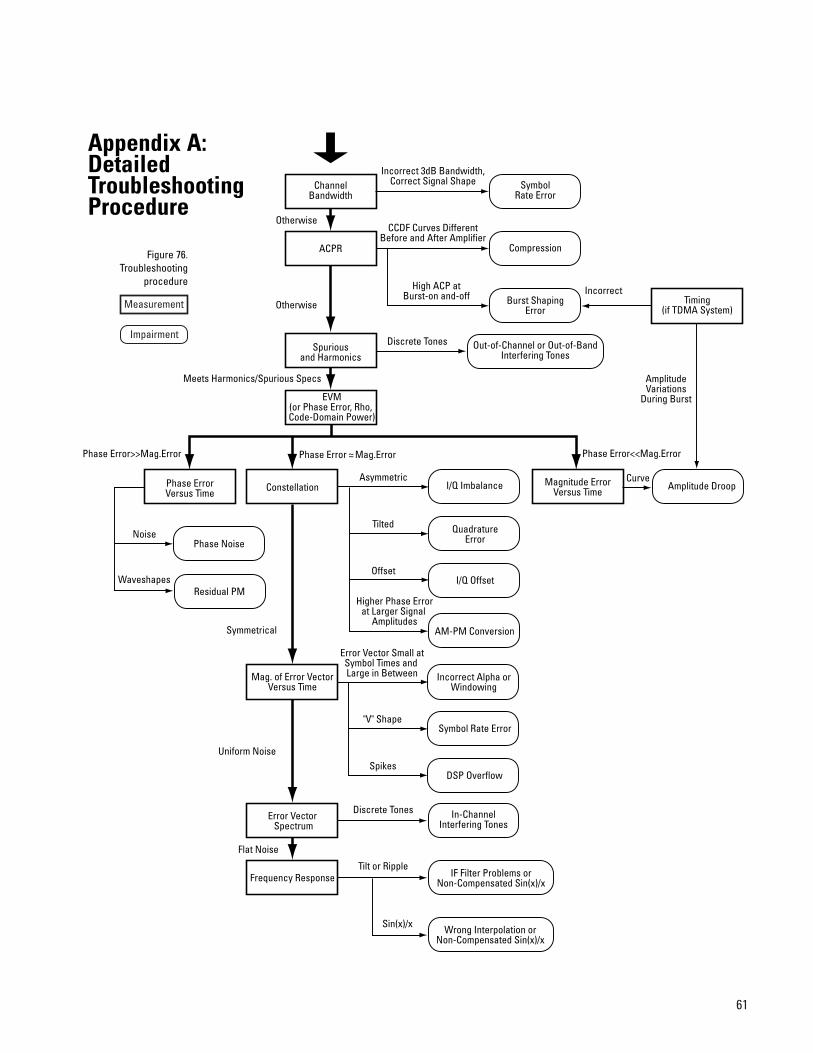
61
ACPR
ChannelBandwidth
EVM(or Phase Error, Rho, Code-Domain Power)
SymbolRate Error
Compression
Burst ShapingError
Timing(if TDMA System)
Out-of-Channel or Out-of-BandInterfering Tones
Residual PM
Phase ErrorVersus Time
Noise
Phase Error>>Mag.Error
Otherwise
Phase Noise
Incorrect 3dB Bandwidth,Correct Signal Shape
CCDF Curves DifferentBefore and After Amplifier
High ACP atBurst-on and-off Incorrect
Waveshapes
Otherwise
Discrete Tones
Asymmetric
Tilted
Offset
Higher Phase Errorat Larger Signal
Amplitudes
I/Q Imbalance
QuadratureError
I/Q Offset
AM-PM Conversion
CurveAmplitude DroopMagnitude Error
Versus Time
Phase Error<<Mag.Error
Error Vector Small atSymbol Times and Large in Between
"V" Shape
Spikes
Incorrect Alpha orWindowing
Symbol Rate Error
DSP Overflow
Phase Error Mag.Error
Constellation
Symmetrical
Uniform Noise
Mag. of Error VectorVersus Time
Frequency Response
Error Vector Spectrum
In-ChannelInterfering Tones
IF Filter Problems orNon-Compensated Sin(x)/x
Wrong Interpolation orNon-Compensated Sin(x)/x
Flat Noise
Discrete Tones
Tilt or Ripple
Sin(x)/x
Spuriousand Harmonics
Meets Harmonics/Spurious Specs AmplitudeVariations
During Burst
Appendix A:DetailedTroubleshootingProcedure
Figure 76. Troubleshooting
procedure
Measurement
Impairment
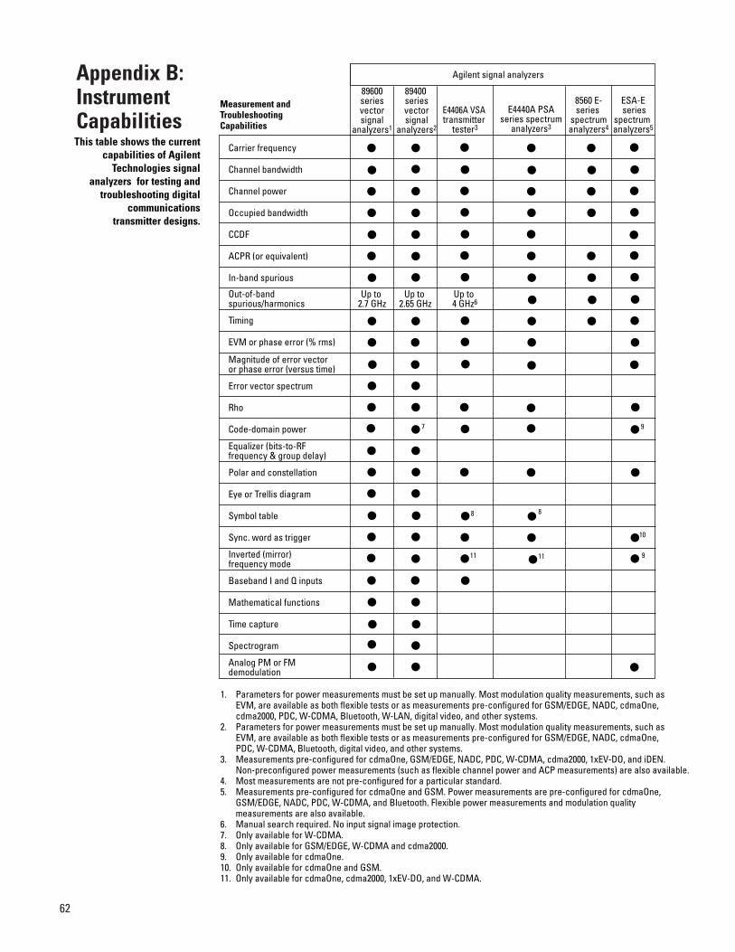
62
Appendix B:Instrument Capabilities
Carrier frequency
Channel bandwidth
Channel power
Occupied bandwidth
CCDF
ACPR (or equivalent)
In-band spurious
Out-of-bandspurious/harmonics
Timing
EVM or phase error (% rms)
Magnitude of error vector or phase error (versus time)
Error vector spectrum
Rho
Code-domain power
Equalizer (bits-to-RF frequency & group delay)
Polar and constellation
Eye or Trellis diagram
Symbol table
Sync. word as trigger
Inverted (mirror)frequency mode
Baseband I and Q inputs
Mathematical functions
Time capture
Spectrogram
Analog PM or FM demodulation
E4406A VSA transmitter
tester3
E4440A PSAseries spectrum
analyzers3
8560 E-series
spectrumanalyzers4
ESA-E series
spectrum analyzers5
Up to 2.7 GHz
Up to 2.65 GHz
Up to 4 GHz6
Agilent signal analyzers
Measurement andTroubleshootingCapabilities
7 9
10
8 8
11 11 9
1. Parameters for power measurements must be set up manually. Most modulation quality measurements, such as EVM, are available as both flexible tests or as measurements pre-configured for GSM/EDGE, NADC, cdmaOne, cdma2000, PDC, W-CDMA, Bluetooth, W-LAN, digital video, and other systems.
2. Parameters for power measurements must be set up manually. Most modulation quality measurements, such as EVM, are available as both flexible tests or as measurements pre-configured for GSM/EDGE, NADC, cdmaOne, PDC, W-CDMA, Bluetooth, digital video, and other systems.
3. Measurements pre-configured for cdmaOne, GSM/EDGE, NADC, PDC, W-CDMA, cdma2000, 1xEV-DO, and iDEN. Non-preconfigured power measurements (such as flexible channel power and ACP measurements) are also available.
4. Most measurements are not pre-configured for a particular standard.5. Measurements pre-configured for cdmaOne and GSM. Power measurements are pre-configured for cdmaOne,
GSM/EDGE, NADC, PDC, W-CDMA, and Bluetooth. Flexible power measurements and modulation quality measurements are also available.
6. Manual search required. No input signal image protection. 7. Only available for W-CDMA.8. Only available for GSM/EDGE, W-CDMA and cdma2000. 9. Only available for cdmaOne.10. Only available for cdmaOne and GSM.11. Only available for cdmaOne, cdma2000, 1xEV-DO, and W-CDMA.
89400 series
vector signal
analyzers2
89600series
vector signal
analyzers1
This table shows the currentcapabilities of Agilent
Technologies signal analyzers for testing and
troubleshooting digital communications
transmitter designs.
63
3G . . . . . . . . . . . . . . . . . . . . . . . . . . . . . . . . . . . . . . . . . . . . . . . . . . . . . . . . Third GenerationACP . . . . . . . . . . . . . . . . . . . . . . . . . . . . . . . . . . . . . . . . . . . . . . . . Adjacent Channel Power ACPR . . . . . . . . . . . . . . . . . . . . . . . . . . . . . . . . . . . . . . . . . . Adjacent Channel Power Ratiobits-to-RF frequency response . . . . . . . . . . . . . . . Frequency response from baseband
to RF, using bits as the stimulus signal BW . . . . . . . . . . . . . . . . . . . . . . . . . . . . . . . . . . . . . . . . . . . . . . . . . . . . . . . . . . . . . BandwidthCCDF . . . . . . . . . . . . . . . . . . . . . . . . . Complementary Cumulative Distribution FunctionCDMA. . . . . . . . . . . . . . . . . . . . . . . . . . . . . . . . . . . . . . . . . . Code Division Multiple AccesscdmaOne . . . . . . . . . . . . . . . . . . . . . . . . . . . . . . . . . . . IS-95 standard-based CDMA systemcdma2000. . . . . . . . . . . . . . . . . . . . . . . . . . . . . . . . . . . . . . cdmaOne derivative, 3G systemCMOS . . . . . . . . . . . . . . . . . . . . . . . . . . . . . . Complementary Metal Oxide SemiconductorDAC . . . . . . . . . . . . . . . . . . . . . . . . . . . . . . . . . . . . . . . . . . . . . . Digital-to-Analog ConverterDECT . . . . . . . . . . . . . . . . . . . . . . . . . . . . . . . . . . . . Digital Enhanced Cordless TelephoneDSP. . . . . . . . . . . . . . . . . . . . . . . . . . Digital Signal Processor or Digital Signal ProcessingDVB-C . . . . . . . . . . . . . . . . . . . . . . . . . . . . . . . . . . . . . . . . . Digital Video Broadcast - CableEVM . . . . . . . . . . . . . . . . . . . . . . . . . . . . . . . . . . . . . . . . . . . . . . . . . Error Vector MagnitudeFFT. . . . . . . . . . . . . . . . . . . . . . . . . . . . . . . . . . . . . . . . . . . . . . . . . . Fast Fourier TransformFIR . . . . . . . . . . . . . . . . . . . . . . . . . . . . . . . . . . . . . . . . . . . . . . . . . Finite Impulse ResponseFM . . . . . . . . . . . . . . . . . . . . . . . . . . . . . . . . . . . . . . . . . . . . . . . . . . . Frequency Modulationframe . . . . . . . . . . . . . . . . . . . . . . . . . . . . . . . In TDMA systems, a repeating time interval
divided among multiple users (see timeslot) GSM . . . . . . . . . . . . . . . . . . . . . . . . . . . . . . . . . Global System for Mobile communicationsGMSK . . . . . . . . . . . . . . . . . . . . . . . . . . . . . . . . . . . . . . . . Gaussian Minimum Shift KeyingIF . . . . . . . . . . . . . . . . . . . . . . . . . . . . . . . . . . . . . . . . . . . . . . . . . . . Intermediate FrequencyI/Q . . . . . . . . . . . . . . . . . . . . . . . . . . . . . . . . . . . . . . . . . . . . . . . . . . . . . In-phase/QuadratureISI . . . . . . . . . . . . . . . . . . . . . . . . . . . . . . . . . . . . . . . . . . . . . . . . . Intersymbol InterferenceLMDS. . . . . . . . . . . . . . . . . . . . . . . . . . . . . . . . . . . . . Local Multipoint Distribution SystemLO . . . . . . . . . . . . . . . . . . . . . . . . . . . . . . . . . . . . . . . . . . . . . . . . . . . . . . . . . Local OscillatorMSB . . . . . . . . . . . . . . . . . . . . . . . . . . . . . . . . . . . . . . . . . . . . . . . . . . . . Most Significant BitNADC . . . . . . . . . . . . . . . . . . . . . . . . . . . . . . . . . . North American Digital Cellular systemOQPSK . . . . . . . . . . . . . . . . . . . . . . . . . . . . . . . . . . . Offset Quadrature Phase Shift KeyingORFS . . . . . . . . . . . . . . . . . . . . . . . . . . . . . . . . . . . . . . . . . . . . . . . . . . Output RF Spectrum PA . . . . . . . . . . . . . . . . . . . . . . . . . . . . . . . . . . . . . . . . . . . . . . . . . . . . . . . . . Power AmplifierPDC . . . . . . . . . . . . . . . . . . . . . . . . . . . . . . . . . . . . . . . . . . . . Pacific Digital Cellular systemPHS . . . . . . . . . . . . . . . . . . . . . . . . . . . . . . . . . . . . . . . . . . . . Personal Handyphone SystemPM . . . . . . . . . . . . . . . . . . . . . . . . . . . . . . . . . . . . . . . . . . . . . . . . . . . . . . . Phase ModulationRF . . . . . . . . . . . . . . . . . . . . . . . . . . . . . . . . . . . . . . . . . . . . . . . . . . . . . . . . Radio FrequencySA. . . . . . . . . . . . . . . . . . . . . . . . . . . . . . . . . . . . . . . . . . . . . . . . . . . . . . . Spectrum Analyzer SAW . . . . . . . . . . . . . . . . . . . . . . . . . . . . . . . . . . . . . . . . . . . . . . . . . . Surface Acoustic Wave TDMA . . . . . . . . . . . . . . . . . . . . . . . . . . . . . . . . . . . . . . . . . . Time Division Multiple Accesstimeslot . . . . . . . . . . . . . . . . . . . . . . . . . . . . In TDMA systems, amount of time per frame
each mobile has to transmit information (see frame)VSA . . . . . . . . . . . . . . . . . . . . . . . . . . . . . . . . . . . . . . . . . . . . . . . . . . Vector Signal Analyzer Walsh code . . . . . . . . . . . Orthogonal code used in cdmaOne systems for channelization
in the forward link and as orthogonal modulation in the reverse linkW-CDMA . . . . . . . . . . . . . . . . . . . . . . . . . . . . . . . . . . . . . . . . . Wideband CDMA, 3G system
5. Glossary
64
6. References
[1] Digital Modulation in Communications Systems,
Application Note 1298, literature number 5965-7160E.[2] Understanding CDMA Measurements for
Base Stations and Their Components,
Application Note 1311, literature number 5968-0953E.[3] Understanding GSM Transmitter Measurements for
Base Transceiver Stations and Mobile Stations,
Application Note 1312, literature number 5968-2320E.[4] Understanding PDC and NADC Transmitter
Measurements for Base Transceiver Stations and
Mobile Stations, Application Note 1324, literature number 5968-5537E.
[5] Testing and Troubleshooting Digital
RF Communications Receiver Designs,
Application Note 1314, literature number 5968-3579E.[6] Power Statistics of Digitally Modulated Signals,
Pete Watridge,Wireless Symposium, 1999.[7] Adaptive Equalization and Modulation Quality,
Bob Cutler, Hewlett-Packard Wireless R&D Seminar, 1997.[8] Spectrum Analyzer Measurements and Noise,
Application Note 1303, literature number 5966-4008E.
7. Related Literature
1. Using Vector Modulation Analysis in the Integration,
Troubleshooting and Design of Digital RF
Communications Systems,
Product Note 89400-8, literature number 5091-8687E.2. Using Error Vector Magnitude Measurements to Analyze
and Troubleshoot Vector-Modulated Signals,
Product Note 89400-14, literature number 5965-2898E.3. 89400 Series Vector Signal Analyzers,
literature number 5965-8554E.4. VSA Series Transmitter Tester,
literature number 5966-4762E.5. 8560 E-Series Spectrum Analyzers,
literature number 5966-3559E.6. 8590 E-Series Spectrum Analyzers,
literature number 5963-6908E.7. ESA-E Series Spectrum Analyzers,
literature number 5968-3278E.
Agilent Technologies’ Test and Measurement Support,Services, and AssistanceAgilent Technologies aims to maximize the value youreceive, while minimizing your risk and problems. Westrive to ensure that you get the test and measurementcapabilities you paid for and obtain the support youneed. Our extensive support resources and services canhelp you choose the right Agilent products for yourapplications and apply them successfully. Every instru-ment and system we sell has a global warranty. Supportis available for at least five years beyond the productionlife of the product. Two concepts underlie Agilent’soverall support policy: “Our Promise” and “YourAdvantage.”
Our PromiseOur Promise means your Agilent test and measurementequipment will meet its advertised performance andfunctionality. When you are choosing new equipment,we will help you with product information, includingrealistic performance specifications and practical rec-ommendations from experienced test engineers. Whenyou use Agilent equipment, we can verify that it worksproperly, help with product operation, and provide basicmeasurement assistance for the use of specified capa-bilities, at no extra cost upon request. Many self-helptools are available.
Your AdvantageYour Advantage means that Agilent offers a wide rangeof additional expert test and measurement services,which you can purchase according to your unique tech-nical and business needs. Solve problems efficientlyand gain a competitive edge by contracting with us forcalibration, extra-cost upgrades, out-of-warrantyrepairs, and on-site education and training, as well asdesign, system integration, project management, andother professional engineering services. ExperiencedAgilent engineers and technicians worldwide can helpyou maximize your productivity, optimize the return oninvestment of your Agilent instruments and systems,and obtain dependable measurement accuracy for thelife of those products.
By internet, phone, or fax, get assistance with all yourtest and measurement needs.
Online assistance:
www.agilent.com/find/assist
Phone or FaxUnited States:(tel) 1 800 452 4844
Canada:(tel) 1 877 894 4414(fax) (905) 282 6495
China:(tel) 800 810 0189(fax) 1 0800 650 0121
Europe:(tel) (31 20) 547 2323(fax) (31 20) 547 2390
Latin America:(tel) (305) 269 7500(fax) (305) 269 7599
Product specificationsand descriptions in thisdocument subject to change without notice.
© Agilent Technologies, Inc. 2002Printed in USA, January 8, 2002
5968-3578E
Japan:(tel) (81) 426 56 7832(fax) (81) 426 56 7840
Korea:(tel) (82 2) 2004 5004 (fax) (82 2) 2004 5115
Taiwan:(tel) 080 004 7866 (fax) (886 2) 2545 6723
Other Asia Pacific Countries:(tel) (65) 375 8100 (fax) (65) 836 0252Email: [email protected]