air interfaces of beyond 3g systems with user...
TRANSCRIPT
Aalborg Universitet
Air Interface of Beyond 3G Systems with User Equipment Hardware Imperfections:Performance & Requirements AspectsPriyanto, Basuki Endah
Publication date:2008
Document VersionOgså kaldet Forlagets PDF
Link to publication from Aalborg University
Citation for published version (APA):Priyanto, B. E. (2008). Air Interface of Beyond 3G Systems with User Equipment Hardware Imperfections:Performance & Requirements Aspects: A case study on UTRA Long Term Evolution Uplink. Aalborg:Department of Electronic Systems, Aalborg University.
General rightsCopyright and moral rights for the publications made accessible in the public portal are retained by the authors and/or other copyright ownersand it is a condition of accessing publications that users recognise and abide by the legal requirements associated with these rights.
? Users may download and print one copy of any publication from the public portal for the purpose of private study or research. ? You may not further distribute the material or use it for any profit-making activity or commercial gain ? You may freely distribute the URL identifying the publication in the public portal ?
Take down policyIf you believe that this document breaches copyright please contact us at [email protected] providing details, and we will remove access tothe work immediately and investigate your claim.
Downloaded from vbn.aau.dk on: oktober 14, 2018

Air Interfaces of Beyond 3G systems withUser Equipment Hardware Imperfections:Performance & Requirements Aspects
A case study on UTRA Long Term Evolution Uplink
Basuki Endah Priyanto
Aalborg University
Denmark
A dissertation submitted for the degree of
Doctor of Philosophy
February 2008

Main supervisors:Troels B. Sørensen, Assoc. Prof, Aalborg University, Denmark
Ole Kiel Jensen, Assoc. Prof, Aalborg University, Denmark
Defence Chairman:Flemming B. Frederiksen, Assoc. Prof, Aalborg University, Denmark
Opponents:Mark Beach, Prof. , Bristol University, UK
Kari Pajukoski, Senior Specialist, Nokia Siemens Networks Finland
Jan H. Mikkelsen, Assoc. Prof, Aalborg University, Denmark
ISBN: 978-87-92328-09-0
Aalborg University
Department of Electronic Systems
Niels Jernes Vej 12, DK-9220 Aalborg, Denmark
Phone +45 96358600, Fax +45 98151583
www.es.aau.dk
c©Copyright 2008, Basuki Endah Priyanto
All rights reserved. The work may not be reposted without the explicit permission
of the copyright holder.

To my wife Dina and my parents.

“ Whoever treads a path seeking knowledge therein, Allah directs him to apath leading to paradise.”
-Sahih Muslim Hadith-

Summary
Orthogonal Frequency Division Multiple Access (OFDMA) and Single-CarrierFDMA (SC-FDMA) are the key air interfaces to achieve high spectral efficiencyfor UTRA Long Term Evolution (LTE) system, which is also known as the be-yond 3rd generation (B3G) system. The selection of air interface techniques isinfluenced by the RF transmitter constraints, i.e. the hardware imperfections.The RF transmitter imperfections create in-band performance degradation andincrease the out-of-band emissions. The latter can lead to violate Spectral Emis-sion Mask (SEM) and Adjacent Channel Leakage Ratio (ACLR) requirements.This thesis deals with the air interface design of beyond 3G systems to achievehigh spectral efficiency, and the impact of the imperfections on both performanceand the transmitter requirements.
Baseline performance results without the imperfections show that OFDMA isgenerally better than SC-FDMA with a Minimum Mean Square Error (MMSE)receiver. Depending on the modulation and coding schemes, the performanceof SC-FDMA with turbo equalizer becomes better or equal to OFDMA. The ef-fects of well-known RF transmitter imperfections on LTE link level performanceare investigated by simulation. The results show that the Error Vector Magni-tude (EVM) is a good measure to estimate the performance loss for numerousimperfections in the anticipated EVM range. Furthermore, in simulations theseimperfections can be replaced by a white noise source as an equivalent model.As shown, the nonlinear power amplifier is the crucial imperfection affectingthe transmitter design. The hardware imperfections impact on the out of bandspectrum is also investigated. A spectrum shaping technique to control spec-trum emission of the LTE User Equipment (UE) is proposed. The proposedtechnique is capable of controlling the spectrum emission for various bandwidth
iv
settings, and provides good trade-off between spectrum emission control, per-formance loss, and implementation complexity. While all these investigationswere done for the most common transmitter architecture - the cartesian type- an investigation was similarly done for the impact of the polar transmitterimperfections on LTE performance. The polar transmitter is a candidate forthe future RF transmitter architecture to realize highly efficient power ampli-fication. Similarly here, the results show that the EVM measurement resultscan be used to estimate the performance loss. As a final topic, the in-bandinterference effects on LTE resource block allocation are investigated. The UE’stransmit signal leakage within the in-band channel cannot be controlled by thetransmitter shaping filter and therefore create interference. The results showthat the Radio Resource Management (RRM) functionality should take careto place the UE resource block allocation to avoid a significant performanceloss due to the leakage generated by the RF imperfections and different PowerSpectral Density (PSD) level among UEs.
In general, it is important that the out-of-band emission meet the SEM andACLR requirements. Therefore, the in-band performance degradation can bekept in the acceptable level. The results confirm that SC-FDMA for the uplinkof B3G system is a good selection as it achieves a high spectral efficiency whilstgaining higher power amplifier efficiency, thereby increasing the cell coverage.
Dansk Resume
(Abstract in Danish)1
Orthogonal Frequency Division Multiple Access (OFDMA) og Single-CarrierFDMA (SC-FDMA) er nøgle transmissionsteknologier i UTRA Long Term Evo-lution (LTE) systemet, ogsa kendt under navnet beyond 3rd generation (B3G)systemet. SC-FDMA er foretrukket til uplink transmission pa grund af dedet la-vere Peak-to-Average Power Ratio (PAPR). Valget af transmissionsteknologierer afhængigt af begrænsninger i RF-trinnet, dvs. ikke-idealiteter i hardwaren.Ikke-idealiteter i RF-trinnet reducerer systemets ydeevne og øger spektralemis-sionen uden for systembandbredden. Sidstnævnte kan føre til overskridelseaf de fastsatte værdier for spektralemission (Spectral Emission Mask - SEM)og nabokanalemission (Adjacent Channel Leakage Ratio - ACLR). Afvejningenmellem implementeringsomkostninger, ikke-idealiteternes indvirkning pa ydeev-nen og overholdelse af SEM og ACLR er vigtige elementer i designet af senderen.
Betragtes ydeevnen uden ikke-idealiteter viser denne afhandling at OFDMAgenerelt set er bedre end SC-FDMA for en Minimum Mean Square Error (MMSE)modtager. Afhængig af modulation og kodning, vil ydeevnen af SC-FDMA medturbo equalizer blive bedre end eller lig med OFDMA. Studier inkluderendekendte RF ikke-idealiteters indvirkning pa LTE link performance viser at Er-ror Vector Magnitude (EVM), indenfor det praktisk anvendelige omrade, er etgodt mal for estimering af tabet i ydeevne for de fleste ikke-idealiteter. Yder-mere viser det sig, at disse ikke-idealiteter kan modelleres ved en hvidstøjs kildesom ækvivalent model. Den ulineære effektforstærker er den væsentligste ikke-idealitet med indvirkning pa designet af senderen. Afhandlingen undersøger
1Translation by Christian Rom, Troels B. Sørensen & Ole K. Jensen, Department of Elec-tronic Systems, Aalborg University Denmark

vi
ogsa indvirkningen af ikke-idealiteter pa spektralemission, og introducerer enfiltreringsteknik for implementering i LTE terminaler til at kontrollere denne.Med denne teknik er det muligt at kontrollere spektralemissionen ved forskel-lige transmissionsbandbredder, med en god afvejning mellem spektralemission,tab i ydeevne og implementeringskompleksitet. Tilsvarende undersøger afhan-dlingen ogsa den nyere polære senderarkitektur med hensyn til ikke-idealitetersindvirkning pa LTE performance. Den polære senderarkitektur kandiderer tilfremtidige RF-arkitekturer pga. dens meget effektive effektforstærkning. Resul-taterne viser at EVM ogsa i denne sammenhæng er et velegnet mal til estimeringaf performance tab. Emissioner inden for transmissionsbandbredden kan ikkekontrolleres ved filtrering hvorfor der vil opsta interferens indenfor systemet.Afhandlingen undersøger derfor de resulterende interferenseffekter med henblikpa LTE radioressourceallokering. Resultaterne viser at ressourceallokeringen,for at undga tab i ydeevne, skal tage hensyn til denne interferens der følger afikke-idealiteter og forskellig spektraleffekttæthed mellem terminaler.
Overordnet set er det vigtigt at overholde de fastsatte værdier for SEM ogACLR. Det er vist at dette er muligt samtidig med at tabet i ydeevne kanholdes indenfor et acceptabelt niveau. Resultaterne viser at SC-FDMA er etgodt valg for B3G uplink idet der opnas en høj spektraleffektivitet sammen medeffektiv effektforstærkning og deraf forbedret radiodækning.
Preface & Acknowledgments
This dissertation is the result of a three years research project carried out atRadio Access Technology Section (RATE) and Technology Platforms Section(TPS), Department of Electronic Systems, Aalborg University. The dissertationhas been completed in parallel with the mandatory courses and teaching/ work-ing obligations required in order to obtain PhD degree. The project has beenconducted under the supervision of Associate Professor Troels B. Sørensen andAssociate Professor Ole K. Jensen and the co-supervision of Professor PrebenE. Mogensen and Professor Torben Larsen. This PhD research project has beensponsored by Aalborg University (Tek NAT) and Center for TeleInfrastruktur(CTIF), Denmark.
My deepest gratitude to my supervisors for their guidance, encouragement andwise advices during the completion of this PhD work. Also, I would like tothank my co-supervisors for their insightful suggestions towards my study. ThisPhD study has significant impact to my life from both personal and professionalpoint of view. Further, I would like to thank the members of the assessmentcommittee who through their detailed reading and constructive feedback havehelped in the correction and clarification of the text throughout this dissertation.
I would like to express my gratitude to my colleagues and former PhD studentsin both RATE and TPS section. Thanks to Lisbeth S. Larsen and Jytte Larsenfor the constant support, assistance, and the proofreading. Many appreciationsare paid to Christian Rom, Akhilesh Pokhariyal, Wei Na, Carles Navarro, andGilberto Berardinelli for their fruitful discussions and help in the link levelstudies. Further, I want to thank my RISC colleagues Tian Tong, NastaranBehjou, Yong Hui, and Jorge Martires. A special thanks goes to my former

viii
diligent students Humbert Codina, Sergi Rene, and Danish Khan.
My sincere appreciation goes to the members of Radio System Technology, NokiaSiemens Networks A/S for their contribution to my personal and professionalgrowth. In particular, thanks to Troels Kolding, Frank Frederiksen, ClaudioRosa, Klaus I. Pedersen, and Istvan Kovacs. It has been a pleasure to worktogether with you and providing me an excellent working environment.
I would like to thank my parents for their encouragement. They deserve thededication of this dissertation. Foremost, I would like to thank my dearest wifeDina for the patient, persistent supports and endless love.
Aalborg, March 2008
Basuki Endah Priyanto

Contents
Summary iii
Dansk Resume v
Preface & Acknowledgments vii
1 Introduction 1
1.1 UTRA Long Term Evolution System (LTE) . . . . . . . . . . . . 2
1.2 State of the Arts on Achieving High Spectral Efficiency . . . . . 5
1.3 Hardware Imperfections: The Limiting Factor . . . . . . . . . . . 7
1.4 Objectives . . . . . . . . . . . . . . . . . . . . . . . . . . . . . . . 10
1.5 Scientific Methodology . . . . . . . . . . . . . . . . . . . . . . . . 11
1.6 Thesis Structure and Contributions . . . . . . . . . . . . . . . . . 13
1.7 Publications . . . . . . . . . . . . . . . . . . . . . . . . . . . . . . 15
2 RF Transmitter Architectures & Imperfections 17
x CONTENTS
2.1 Introduction . . . . . . . . . . . . . . . . . . . . . . . . . . . . . . 17
2.2 Cartesian Transmitter Architectures . . . . . . . . . . . . . . . . 19
2.3 Cartesian Transmitter Imperfections . . . . . . . . . . . . . . . . 25
2.4 Polar Transmitter Architecture . . . . . . . . . . . . . . . . . . . 32
2.5 Polar Transmitter Imperfections . . . . . . . . . . . . . . . . . . 33
2.6 Summary . . . . . . . . . . . . . . . . . . . . . . . . . . . . . . . 35
3 Baseline LTE Uplink Performance Analysis 37
3.1 Introduction . . . . . . . . . . . . . . . . . . . . . . . . . . . . . . 37
3.2 LTE Uplink Numerology . . . . . . . . . . . . . . . . . . . . . . . 38
3.3 Modelling of Radio Access Techniques . . . . . . . . . . . . . . . 41
3.4 Modeling and Validation of LTE uplink Transmitter & Receiver . 44
3.5 Peak-to-Average Power Ratio Evaluation . . . . . . . . . . . . . 44
3.6 Frequency Domain Equalization . . . . . . . . . . . . . . . . . . . 48
3.7 Impact of Link Adaptation . . . . . . . . . . . . . . . . . . . . . 52
3.8 Impact of Fast HARQ . . . . . . . . . . . . . . . . . . . . . . . . 53
3.9 Antenna Configuration . . . . . . . . . . . . . . . . . . . . . . . . 55
3.10 Impact of Frequency Allocation . . . . . . . . . . . . . . . . . . . 56
3.11 Impact of Vehicle Speed . . . . . . . . . . . . . . . . . . . . . . . 59
3.12 Turbo Equalization for Performance Improvement . . . . . . . . 61
3.13 Summary . . . . . . . . . . . . . . . . . . . . . . . . . . . . . . . 64
4 RF Hardware Imperfections Effect on Inband Channel 65
CONTENTS xi
4.1 Introduction . . . . . . . . . . . . . . . . . . . . . . . . . . . . . . 65
4.2 LTE EVM Measurement . . . . . . . . . . . . . . . . . . . . . . . 66
4.3 RF Imperfections Model . . . . . . . . . . . . . . . . . . . . . . . 67
4.4 Evaluation of Inband Performance . . . . . . . . . . . . . . . . . 73
4.5 Summary . . . . . . . . . . . . . . . . . . . . . . . . . . . . . . . 84
5 RF Hardware Imperfections Effect on Out-of-band Channel 87
5.1 Introduction . . . . . . . . . . . . . . . . . . . . . . . . . . . . . . 87
5.2 Out-of-band Channel Requirements . . . . . . . . . . . . . . . . . 88
5.3 Spectrum Shaping Techniques . . . . . . . . . . . . . . . . . . . . 90
5.4 Assumptions & Scenarios on Controlling Out-of-band Emission . 94
5.5 Spectrum Shaping Performance . . . . . . . . . . . . . . . . . . . 96
5.6 Impact of RF Hardware Imperfections . . . . . . . . . . . . . . . 98
5.7 Summary . . . . . . . . . . . . . . . . . . . . . . . . . . . . . . . 105
6 Polar Transmitter for LTE Uplink 107
6.1 Introduction . . . . . . . . . . . . . . . . . . . . . . . . . . . . . . 107
6.2 Modeling Assumptions . . . . . . . . . . . . . . . . . . . . . . . . 108
6.3 PA Non-idealities . . . . . . . . . . . . . . . . . . . . . . . . . . . 110
6.4 Inband Performance . . . . . . . . . . . . . . . . . . . . . . . . . 111
6.5 Out-of-band Performance . . . . . . . . . . . . . . . . . . . . . . 116
6.6 Summary . . . . . . . . . . . . . . . . . . . . . . . . . . . . . . . 120
7 Inband Inter-User Interference Analysis 123

xii CONTENTS
7.1 Introduction . . . . . . . . . . . . . . . . . . . . . . . . . . . . . . 123
7.2 Description of Multi-user Modeling . . . . . . . . . . . . . . . . . 124
7.3 Interference Sources . . . . . . . . . . . . . . . . . . . . . . . . . 126
7.4 Modeling Assumptions . . . . . . . . . . . . . . . . . . . . . . . . 128
7.5 Impact of Frequency Offset and PSD offset . . . . . . . . . . . . 130
7.6 Impact of Phase Noise and PSD Offset . . . . . . . . . . . . . . . 135
7.7 Proposed Solution . . . . . . . . . . . . . . . . . . . . . . . . . . 138
7.8 Summary . . . . . . . . . . . . . . . . . . . . . . . . . . . . . . . 138
8 Conclusion 141
8.1 Main Findings and Contributions . . . . . . . . . . . . . . . . . . 142
8.2 Recommendations . . . . . . . . . . . . . . . . . . . . . . . . . . 143
8.3 Future Work . . . . . . . . . . . . . . . . . . . . . . . . . . . . . 144
A LTE Uplink Link Level Simulator: Descriptions & Validation 145
A.1 Descriptions . . . . . . . . . . . . . . . . . . . . . . . . . . . . . . 145
A.2 Validation . . . . . . . . . . . . . . . . . . . . . . . . . . . . . . . 150
B Channel Model 155
C Turbo Equalizer 159
C.1 System Model . . . . . . . . . . . . . . . . . . . . . . . . . . . . . 159
C.2 Turbo Equalization . . . . . . . . . . . . . . . . . . . . . . . . . . 162
C.3 SIC Equalizer Coefficients . . . . . . . . . . . . . . . . . . . . . . 165

CONTENTS xiii
Bibliography 176

xiv CONTENTS
List of Figures
1.1 The Evolution of Wireless Cellular System [1]. . . . . . . . . . . 3
1.2 3GPP release specifications towards 4G system. . . . . . . . . . . 3
1.3 Frequency-Time representation of an OFDM signal [2]. . . . . . . 6
1.4 Hardware imperfections in the RF part limit the system levelperformance. . . . . . . . . . . . . . . . . . . . . . . . . . . . . . 8
1.5 Work-scopes of the research project. . . . . . . . . . . . . . . . . 11
2.1 Cartesian superheterodyne RF transmitter architecture. . . . . . 19
2.2 The direct conversion (homodyne) RF transmitter architecture. . 22
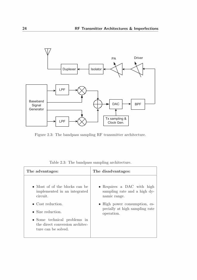
2.3 The bandpass sampling RF transmitter architecture. . . . . . . . 24
2.4 The power amplifier output signal characteristic. . . . . . . . . . 27
2.5 Measure of spurious free dynamic range [3]. . . . . . . . . . . . . 31
2.6 Polar EER transmitter architecture. . . . . . . . . . . . . . . . . 32
2.7 Imperfections model in a polar transmitter. . . . . . . . . . . . . 35
xvi LIST OF FIGURES
3.1 LTE uplink sub-frame structure with 2 short blocks. . . . . . . . 39
3.2 LTE uplink slot structure with 1 short block. . . . . . . . . . . . 39
3.3 OFDMA & SC-FDMA basic transmitter & receiver structure. . . 41
3.4 Layer-1 UTRA LTE uplink link level simulator . . . . . . . . . . 45
3.5 PAPR of SC-FDMA with various modulation schemes. . . . . . . 46
3.6 PAPR of OFDM for various modulation schemes. . . . . . . . . . 46
3.7 PAPR comparison of SC-FDMA and OFDMA. . . . . . . . . . . 47
3.8 PAPR of SC-FDMA & OFDMA for different numbers of subcar-riers. . . . . . . . . . . . . . . . . . . . . . . . . . . . . . . . . . . 48
3.9 BLER performance of BPSK 1/6 SC-FDMA & OFDMA withdifferent equalization. . . . . . . . . . . . . . . . . . . . . . . . . 49
3.10 BLER performance of 16QAM 4/5 SC-FDMA & OFDMA withdifferent equalization. . . . . . . . . . . . . . . . . . . . . . . . . 50
3.11 Spectral efficiency of SC-FDMA with Zero Forcing equalization. . 51
3.12 Spectral efficiency of SC-FDMA with MMSE equalization. . . . . 51
3.13 Spectral efficiency of SISO SC-FDMA with various MCS schemes. 52
3.14 Spectral efficiency of SC-FDMA SISO case for chase combining(CC) and incremental redundancy (IR). . . . . . . . . . . . . . . 54
3.15 Spectral efficiency of SC-FDMA SISO case with HARQ. . . . . . 55
3.16 Spectral efficiency for SC-FDMA and OFDMA with two antennaconfigurations (SISO and SIMO). . . . . . . . . . . . . . . . . . . 57
3.17 CDF of measured instantaneous SNR of SC-FDMA. . . . . . . . 57
3.18 Localized and distributed frequency allocation in LTE uplink. . . 58
3.19 BLER performance of Distributed versus Localized in SC-FDMA. 59
LIST OF FIGURES xvii
3.20 SC-FDMA and OFDMA with real channel estimation at speedof 120 km/h. . . . . . . . . . . . . . . . . . . . . . . . . . . . . . 60
3.21 SC-FDMA and OFDMA with real channel estimation at speedof 200 km/h. . . . . . . . . . . . . . . . . . . . . . . . . . . . . . 60
3.22 BLER performance for SC-FDMA 1x2 MRC with and withoutTurbo Equalizer in TU 06 channel. . . . . . . . . . . . . . . . . . 62
3.23 BLER performance for SC-FDMA versus OFDMA in TU 06channel. . . . . . . . . . . . . . . . . . . . . . . . . . . . . . . . . 62
3.24 Spectral efficiency for SC-FDMA in TU 06 channel. . . . . . . . 63
4.1 SC-FDMA modulation/demodulation and EVM measurement point. 68
4.2 Measured AM/AM, AM/PM (asteriks) and model fit (solid) ver-sus source power (dBm) [4]. . . . . . . . . . . . . . . . . . . . . . 69
4.3 Phase noise power spectral density . . . . . . . . . . . . . . . . . 72
4.4 EVM results for Nonlinear PA . . . . . . . . . . . . . . . . . . . 75
4.5 EVM results for different RB size in SC-FDMA (16QAM) withnonlinear PA . . . . . . . . . . . . . . . . . . . . . . . . . . . . . 76
4.6 Spectral efficiency degradation for various MCS in the presenceof nonlinear PA . . . . . . . . . . . . . . . . . . . . . . . . . . . . 77
4.7 Performance loss at 10% BLER due to the nonlinear PA . . . . . 78
4.8 EVM results for various RF Imperfections . . . . . . . . . . . . . 79
4.9 Throughput degradation for 16QAM 3/4 in AWGN channel dueto the transmitter with a white noise source imperfection. . . . . 80
4.10 Approximating the maximum capacity of MCS envelope in AWGNChannel. . . . . . . . . . . . . . . . . . . . . . . . . . . . . . . . . 81
4.11 SNR loss for 16QAM 3/4 due to the RF imperfections (AWGN). 82
4.12 SNR loss for 16QAM 4/5 due to the RF imperfections (AWGN). 83
xviii LIST OF FIGURES
4.13 SNR loss for 16QAM 3/4 due to the RF imperfections (TU06). . 83
4.14 SNR loss for 16QAM 4/5 due to the RF imperfections (TU06). . 84
5.1 Channelization of the transmit spectrum. . . . . . . . . . . . . . 90
5.2 SC-FDMA transmitter structures with spectrum shaping. . . . . 91
5.3 Inverse Chebyshev filter frequency response for 10 MHz systembandwidth. . . . . . . . . . . . . . . . . . . . . . . . . . . . . . . 93
5.4 Time windowing process of the SC-FDMA symbol. . . . . . . . . 93
5.5 Spectrum emission with & without spectrum shaping for 10 MHzsystem bandwidth. . . . . . . . . . . . . . . . . . . . . . . . . . . 96
5.6 Spectrum emission of 1.25 MHz system bandwidth. . . . . . . . . 97
5.7 EVM results for various bandwidth settings (a) and time win-dowing with different overlapped window samples (b). . . . . . . 99
5.8 Spectrum emission of SC-FDMA & OFDMA. . . . . . . . . . . . 100
5.9 ACLR results of SC-FDMA with Nonlinear Amplifier. . . . . . . 101
5.10 ACLR results of OFDMA with Nonlinear Amplifier. . . . . . . . 101
5.11 Summary of SC-FDMA and OFDMA ACLR results. . . . . . . . 102
5.12 Spectrum emission of a transmitter (10 MHz) with imperfectionsas given in Table 5.3. . . . . . . . . . . . . . . . . . . . . . . . . . 103
5.13 ACLR results of a transmitter (10MHz) with and without imper-fections as given in Table 5.3. . . . . . . . . . . . . . . . . . . . . 103
5.14 Spectrum emission of a transmitter (1.4 MHz) with imperfectionsas given in Table 5.3. . . . . . . . . . . . . . . . . . . . . . . . . . 104
5.15 ACLR results of a transmitter (1.4 MHz) with and without im-perfections. . . . . . . . . . . . . . . . . . . . . . . . . . . . . . . 105
6.1 Polar transmitter imperfections model for LTE uplink. . . . . . . 109

LIST OF FIGURES xix
6.2 AM/AM impact on the output signal. . . . . . . . . . . . . . . . 110
6.3 AM/PM & signal leakage impact on the output signal. . . . . . . 111
6.4 Maximum achievable spectral efficiency for various MCS. . . . . 112
6.5 EVM results for various polar transmitter imperfections. . . . . . 113
6.6 EVM results for limited bandwidth. . . . . . . . . . . . . . . . . 114
6.7 Spectral efficiency degradation for 16QAM rate 3/4 due to thesignal leakage. . . . . . . . . . . . . . . . . . . . . . . . . . . . . . 115
6.8 SNR loss for 16QAM rate 3/4 in AWGN channel. . . . . . . . . . 115
6.9 SNR loss for 16QAM rate 3/4 in TU06 channel. . . . . . . . . . . 116
6.10 Impact of timing delay alignment on SC-FDMA spectrum emis-sion (Channel bandwidth 10 MHz). . . . . . . . . . . . . . . . . . 117
6.11 ACLR results for SC-FDMA with imperfect timing delay alignment.118
6.12 Impact of limited bandwidth in the envelope path. . . . . . . . . 118
6.13 ACLR results on the limited bandwidth in the envelope path. . . 119
6.14 ACLR for different imperfections at EVM=4%. . . . . . . . . . . 120
7.1 System model of the multi-user environment (3 UEs) in LTE uplink.125
7.2 Received Power Spectral Density (PSD) of 3 UEs at the base-station. . . . . . . . . . . . . . . . . . . . . . . . . . . . . . . . . 127
7.3 Received PSD of each UE in 10 MHz system bandwidth. . . . . . 130
7.4 EVM results at different PSD level and frequency offset for dif-ferent RB size. . . . . . . . . . . . . . . . . . . . . . . . . . . . . 131
7.5 BLER results for 5 RBs transmission (Victim UE) in AWGNchannel. . . . . . . . . . . . . . . . . . . . . . . . . . . . . . . . . 132
7.6 Frequency offset and PSD effects (SNRloss)to the in-band inter-ference in AWGN channel for different RB size . . . . . . . . . . 133

xx LIST OF FIGURES
7.7 Frequency offset and PSD offset effects (SNRloss) in the in-bandinterference in Typical Urban channel for different RB size. . . . 134
7.8 Phase noise effect (SNRloss) in the in-band interference in AWGNchannel for different RB size . . . . . . . . . . . . . . . . . . . . . 136
7.9 Phase noise effect (SNRloss) in the in-band interference in Typ-ical Urban channel for different RB size . . . . . . . . . . . . . . 137
7.10 UE frequency domain scheduling solution to avoid large PSD offset138
A.1 Layer 1 UTRA LTE uplink Link Level Simulator . . . . . . . . . 147
A.2 Uncoded BER results of QPSK in AWGN. . . . . . . . . . . . . . 150
A.3 Uncoded BER results of 16QAM in AWGN. . . . . . . . . . . . . 151
A.4 Comparison of BLER results in AWGN channel. . . . . . . . . . 151
A.5 Comparison of BLER results in Typical Urban Channel. . . . . . 152
A.6 HARQ Chase Combining and Incremental Redundancy. . . . . . 153
A.7 Spectral Efficiency for 16QAM 3/4 in Typical Urban Channel. . 153
B.1 Frequency correlation property of Typical Urban Channel Model. 157
C.1 SC-FDMA transmitter . . . . . . . . . . . . . . . . . . . . . . . . 160
C.2 Turbo equalizer structure . . . . . . . . . . . . . . . . . . . . . . 161

List of Tables
2.1 The superheterodyne architecture. . . . . . . . . . . . . . . . . . 21
2.2 The direct conversion architecture. . . . . . . . . . . . . . . . . . 23
2.3 The bandpass sampling architecture. . . . . . . . . . . . . . . . . 24
3.1 Parameters for LTE uplink [5] . . . . . . . . . . . . . . . . . . . . 40
3.2 UTRA LTE uplink simulation parameters. . . . . . . . . . . . . . 49
3.3 Peak Data Rate For 10 MHz System . . . . . . . . . . . . . . . . 53
4.1 UTRA LTE uplink simulation parameters. . . . . . . . . . . . . . 74
5.1 UTRA Spectrum Emission Mask Requirement (SEM) [6]. . . . . 89
5.2 LTE uplink Transmission Parameters. . . . . . . . . . . . . . . . 94
5.3 Simulation Parameters. . . . . . . . . . . . . . . . . . . . . . . . 95
7.1 Phase Noise Characteristics. . . . . . . . . . . . . . . . . . . . . . 129
7.2 Multi-user link level simulation parameters. . . . . . . . . . . . . 129

xxii List of Abbreviations
B.1 Typical Urban Channel Power Delay Profile. . . . . . . . . . . . 156
List of Abbreviations
3GPP Third Generation Partnership ProjectACLR Adjacent Channel Leakage RatioADC Analog to Digital ConverterAGC Automatic Gain ControlAM/AM Amplitude Modulation/Amplitude ModulationAM/PM Amplitude Modulation/Phase ModulationAMC Adaptive Modulation and CodingARQ Automated Repeat reQuestAWGN Additive White Gaussian NoiseB3G Beyond the 3rd GenerationBB BasebandBER Bit Error RateBLER Block Error RateBPF Bandpass FilterCDMA Code Division Multiple AccessCCDF Cumulative Complementary Distribution FunctionCP Ciclic PrefixCRC Cyclic Redundancy CheckDAC Digital to Analog ConverterDFT-s-OFDM DFT-Spread OFDMDL DownlinkEER Envelope Elimination and RestorationEDGE Enhanced Data rates for Global EvolutionEUTRA Evolved UMTS Terrestrial Radio AccessEvDO Evolution Data OnlyEVM Error Vector Magnitude

xxiv List of Abbreviations
FDD Frequency Division DuplexingFDMA Frequency Division Multiple AccessFFT Fast Fourier TransformGPRS Global Packet Radio ServiceGSM Global System for Mobile CommunicationsH-ARQ Hybrid-ARQHSPA High Speed Packet data AccessICI Inter Carrier InterferenceIDFT Inverse Discrete Fourier TransformIFDM Interleaved Frequency-Division MultiplexingIFDMA Interleaved Frequency-Division MultiplexingIFFT Inverse Fast Fourier TransformISI Inter-Symbol InterferenceLPF Lowpass FilterLO Local OscillatorMC Multi-CarrierMIMO Multiple Input Multiple OutputML Maximum LikelihoddMMSE Minimum Mean-Square-ErrorMRC Maximal Ratio CombiningNLA Non-Linear AmplifierLA Link AdaptationLTE Long Term EvolutionOFDM Orthogonal Frequency-Division MultiplexingOFDMA Orthogonal Frequency-Division Multiple AccessPA Power AmplifierPAE Power Added EfficiencyPAPR Peak-to-Average Power RatioPER Packet Error RatePSK Phase Shift KeyingQAM Quadrature Amplitude ModulationRF Radio FrequencyRC Raised Cosine
xxv
RRM Radio Resource ManagementSAW Surface Acoustic WaveSC Single-CarrierSDR Software Defined RadioSCFDM Single-Carrier Frequency-Division MultiplexingSCFDMA Single-Carrier Frequency-Division Multiple AccessSIMO Single-Input Multiple-OutputSISO Single-Input Single-OutputSNR Signal-to-Noise RatioTDD Time Division DuplexingUE User EquipmentUL UplinkUMTS Universal Mobile Telecommunications SystemUTRAN Universal Terrestrial Radio Access NetworkVHF Very High FrequencyVGA Variable Gain AmplifierWCDMA Wideband CDMAWLAN Wireless Local Area NetworkWimax Wireless Interoperability for Microwave AccessZF Zero-Forcing

xxvi List of Abbreviations
“ A journey of a thousand miles mustbegin with a single step.”
Lao Tze
Chapter 1
Introduction
The research and development of wireless communication systems has beenrapidly growing for the last decades. Multi-carrier technology in the form of Or-thogonal Frequency Division Multiplexing (OFDM), adaptive modulation andcoding, Multiple Input Multiple Output (MIMO) antenna techniques, packetscheduling, link adaptation are the new paradigms in the upcoming wirelesscommunication system to achieve high spectral efficiency and high data ratetransmission. In parallel, The micro-electronic and semiconductor technologiesdevelopment is fastly growing and often refers to Moore’s Law:
”The number of components on a chip will double every eighteen months.”
The synergy between the rapid development of the micro-electronic and semi-conductor technologies and wireless communication research makes the wirelesscommunication algorithms become reality and implemented in the hardware. Itcan easily be observed from the trend of the mobile terminal in a small size withmany features.
The necessity of high data rates wireless communication becomes importantfor the end-user, especially to support high mobility lifestyle ”always get con-nected”, and demand for the multimedia communication, such as the videophone, live streaming, online gaming, and the Internet. For a high data rate
2 Introduction
communication, a high performance mobile terminal or user equipment withminimal RF imperfections is required. It is also essential to maintain low powerconsumption, small physical hardware size, and long duration battery life. Themobile terminal requirement is getting challenging since the price must be keptlow to reach the market. Therefore, the main challenge is to achieve the opti-mum solution.
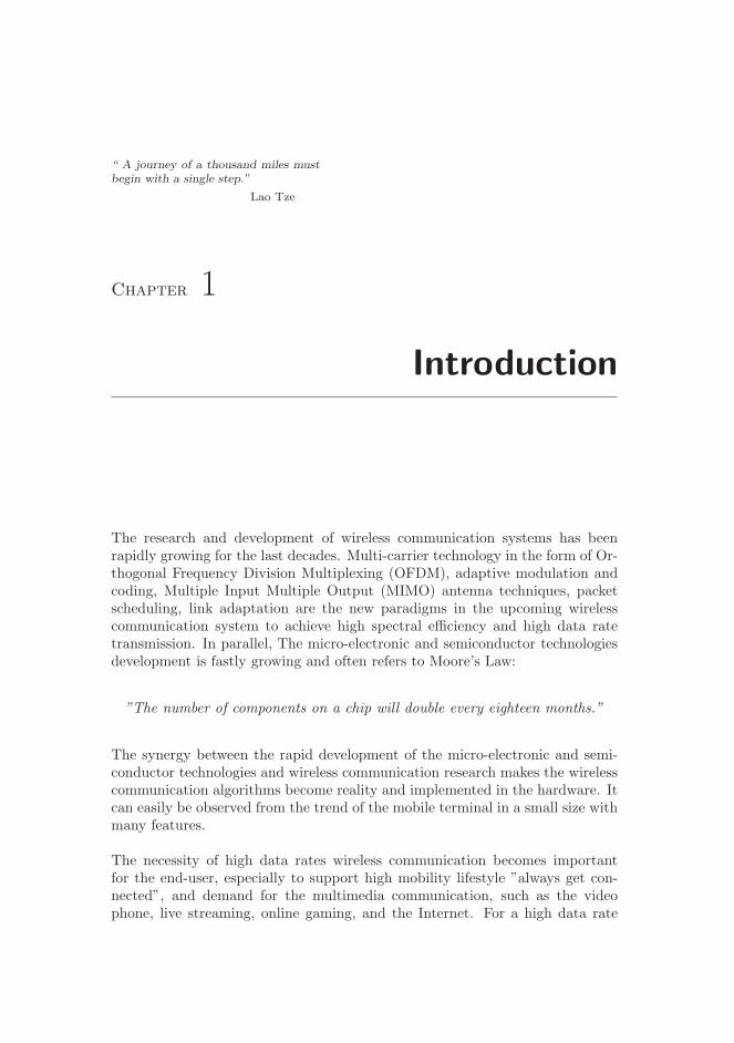
Wireless cellular evolution in the last decade is illustrated in Figure 1.1 [1]. Thesecond generation of the cellular system, GSM evolution started with GPRS,EDGE, and WCDMA. WCDMA in the form of High Speed Downlink PacketAccess (HSDPA) is now widely deployed, and it will still be evolved to the LTEsystem. The CDMA, or mostly known as the second generation for the northAmerica system evolution, started with CDMA2000 1xRTT (Radio Transmis-sion Technology) and then evolved to CDMA EV-DO (EVolution-Data Only)Revision A and finally the EV-DO Revision C. The new standard, Wimax,started from the fixed wireless access before it evolved into the mobile wirelessaccess. Finally, the long term goals of each wireless cellular system are similar,which are aiming at all internet protocol (IP) networks 1with 100 Mbps peakdownlink data-rate and 50 Mbps uplink data-rate [1].
1.1 UTRA Long Term Evolution System (LTE)
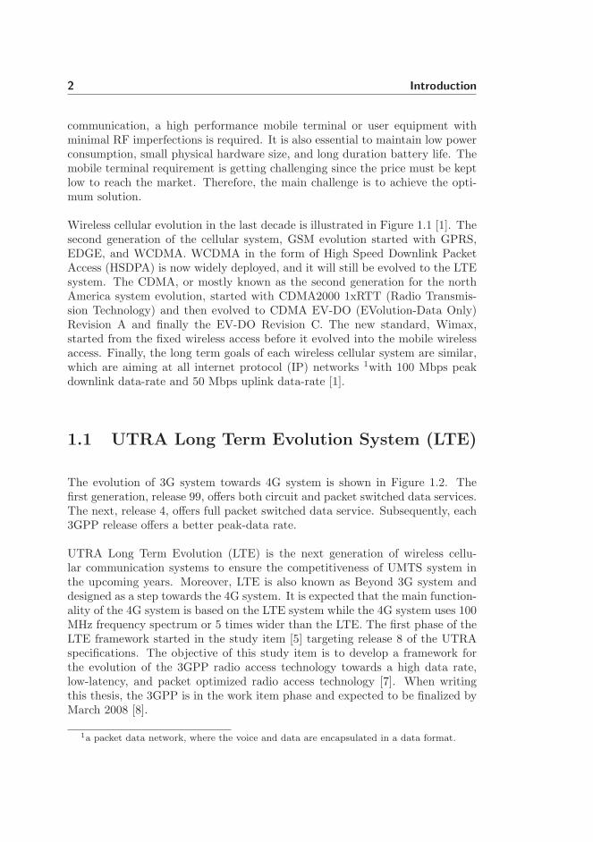
The evolution of 3G system towards 4G system is shown in Figure 1.2. Thefirst generation, release 99, offers both circuit and packet switched data services.The next, release 4, offers full packet switched data service. Subsequently, each3GPP release offers a better peak-data rate.
UTRA Long Term Evolution (LTE) is the next generation of wireless cellu-lar communication systems to ensure the competitiveness of UMTS system inthe upcoming years. Moreover, LTE is also known as Beyond 3G system anddesigned as a step towards the 4G system. It is expected that the main function-ality of the 4G system is based on the LTE system while the 4G system uses 100MHz frequency spectrum or 5 times wider than the LTE. The first phase of theLTE framework started in the study item [5] targeting release 8 of the UTRAspecifications. The objective of this study item is to develop a framework forthe evolution of the 3GPP radio access technology towards a high data rate,low-latency, and packet optimized radio access technology [7]. When writingthis thesis, the 3GPP is in the work item phase and expected to be finalized byMarch 2008 [8].
1a packet data network, where the voice and data are encapsulated in a data format.
UTRA Long Term Evolution System (LTE) 3
2010200920082007200620052004200320022001200010 kbps
100 kbps
1 Mbps
10 Mbps
100 Mbps
Enhanced
EDGE
GPRS
HSDPA
EDGE1xRTT
WCDMARev.0
Rev.A
Enhanced
HSDPA
Rev.B
Wimax
LTE
Wimax
Rev.CGPRS / WCDMA / LTE
CDMA2000 / EVDO
WIMAX
EDGE
Figure 1.1: The Evolution of Wireless Cellular System [1].
3GPP Rel.99
DL:2 Mbps
UL:384 kbps
3GPP Rel.4
DL:2 Mbps
UL:384 kbps3GPP Rel.5
HSDPA
DL:14.4 Mbps
UL:384 kbps
3GPP Rel.6
HSUPA
DL:14.4 Mbps
UL:5.8 Mbps
3GPP Rel.7,
HSPA Evolution
DL:21 Mbps
UL: 12 Mbps 4G
1 Gbps
3G Evolution B3G 4G
5 MHz 20 MHz 100 MHz
3GPP Rel.8
LTE
DL:100 Mbps
UL:50 Mbps
1999 2003 2006 2007 2009 2010 >2010
Figure 1.2: 3GPP release specifications towards 4G system.
4 Introduction
The targets for the evolution of the radio-interface and radio-access networkarchitecture are [7]:
• Significantly increased peak data rate, e.g. 100 Mbps (downlink) and 50Mbps (uplink).
• Increases ”cell edge bit-rate” whilst maintaining the same site locationsas deployed today.
• Significantly improved spectral efficiency over release 6 HSPA e.g. 3-4times for the downlink and 2-3 times for the uplink direction.
• Possibility for a Radio-access network latency below 10 ms.
• Scalable bandwidth:
– 5, 10, 20 and possibly 15 MHz.
– 1.25, 1.6, 2.5 MHz: to allow flexibility in narrow spectral allocationswhere the system may be deployed.
• Support for inter-working with existing 3G systems and non-3GPP speci-fied systems.
• Reasonable system and terminal complexity, cost, and power consumption.
• Efficient support of the various types of services, especially from the PSdomain (e.g. Voice over IP, Presence).
• Support for inter-working with existing 3G systems and non-3GPP speci-fied systems.
• The system should be optimized for low mobile speed, but also supporthigh mobile speed.
Orthogonal Frequency Division Multiple-Access (OFDMA) has been selectedas the multiple access techniques for the LTE downlink and Single-Carrier Fre-quency Division Multiple-Access (SC-FDMA) for uplink. OFDM is recognizedas an attractive modulation technique in a cellular environment because of itscapability to enable low-complexity multipath channel mitigation. Nevertheless,OFDM requires an expensive and inefficient power amplifier in the transmitterdue to the high Peak-to-Average Power Ratio (PAPR) of the multi-carrier sig-nal.
Single Carrier transmission with Cyclic Prefix (SC-CP) is a closely related trans-mission scheme with the same attractive multipath interference mitigation prop-erty as OFDM [9],[10],[11]. Therefore, SC-CP can achieve a performance com-parable to OFDM for the same complexity, but at reduced PAPR. Moreover,
State of the Arts on Achieving High Spectral Efficiency 5
the choice of single carrier transmission in a DFT-Spread OFDM form allowsfor a relatively high degree of commonality with the downlink OFDM schemeand the possibility to use the same system parameters [5].
1.2 State of the Arts on Achieving High Spec-tral Efficiency
High spectral efficiency for achieving high data rate is expected for the LTE.High spectral efficiency can be achieved from the following Layer-1 features. Ingeneral the following Layer-1 features aim at efficiently managing the frequencyand time-slot resource. These are the essential aspects for the Beyond 3G sys-tem on account of the usage of a wideband channel of 20 MHz.
Air InterfacesBoth OFDMA and SC-FDMA are fundamentally based on the OFDM radiotransmission. The OFDM time-frequency representation is shown in Figure 1.3.OFDM technique transmits the information onto several parallel narrow-bandchannels / sub-carriers. Typically, each sub-carrier carries an M-PSK/M-QAMsymbol. The sub-carriers are orthogonal to each other, and a guard interval isadded to each symbol to mitigate inter-symbol interference in frequency selec-tive fading channel. The guard interval length is designed in such a way so thatit is longer than the maximum excess delay of the channel. Therefore, all ofthe multipath components fall within guard interval, and the guard interval willbe removed at the receiver. High spectral efficiency is achieved by allowing thesub-carriers overlap and properly arranged so that the sub-carriers orthogonal-ity can still be maintained.
High User Orthogonality.SC-FDMA transmission allows a high orthogonality among users within a cell.Each user in a cell is allocated in different frequency allocation in the FrequencyDomain Multiplexing (FDM) mode. Therefore, the intra-cell interference whichtypically exists in the 3G system can be avoided.
Short Transmission Time Interval (TTI)In LTE, user transmission is assigned in a 1 ms period. It is much shorter thanthe HSUPA system in a 2 ms period or even significantly shorter than the re-lease 99 system in the order of 10 - 20 ms. The short transmission time intervalallows high dynamic user allocations.
Fast Variable Transmission BandwidthThe uplink transmission bandwidth can be scaled depending on various con-

6 Introduction
…
Sub-carriersFFT
Time
Symbols
System Bandwidth
Guard Intervals
…
Frequency
Figure 1.3: Frequency-Time representation of an OFDM signal [2].
ditions on a TTI basis (1 ms), such as buffer status, QoS requirements, andinstantaneous channel conditions. The minimum transmission bandwidth isone resource block (RB) or 180 kHz, and the maximum one can be the wholetransmission bandwidth in a 20 MHz.
Fast Variable Modulation and Coding SchemesLTE supports various modulation schemes, from QPSK, 16QAM and 64QAM.64QAM is optional for most of the UE classes in LTE uplink [8]. Different mod-ulation and coding rates can be used depending on the channel condition andupdated every TTI. This situation will enable fast link adaptation to achievethe highest possible spectral efficiency on each channel condition.
Fast L1 Hybrid ARQH-ARQ is an automatic repeat request process that has combined the receiveddata block with the previous one in order to increase the likelihood of successfuldecoding [12]. There are two well known H-ARQ with soft combining processes,namely H-ARQ Chase Combining and H-ARQ Incremental Redundancy. Thefast H-ARQ is realized by implementing the medium access mechanism controlin the node-B. The fast H-ARQ can maximize data throughputs, capacity andminimize the delay.
Frequency Domain Channel Aware SchedulingFrequency domain channel aware scheduling is defined with the target of in-creasing user and sector throughput. The frequency allocation is scheduled bythe node-B so that the user frequency allocation is assigned to the frequencyallocation where the user experiences a better channel condition. This situa-tion is also known as multi-user diversity. In LTE uplink the frequency domainchannel aware scheduling requires channel sounding from the UE. Each UE

Hardware Imperfections: The Limiting Factor 7
transmits the sounding reference signal in a wider bandwidth, and the node-Bmeasures the channel statistic indication for each UE. Having the knowledge ofthe channel condition, the UE data transmission can be allocated by the node-B.
Antenna ConfigurationIn LTE the target peak data rates are specified in terms of a reference UEconfiguration comprising:
• Downlink Capability - 2 receive antennas at UE.
• Uplink Capability - 1 transmit antenna at UE.
The above reference is mainly in consequence of the physical size constraint andlimited power at the UE. For the uplink direction, 1x1 SISO and 1x2 SIMOantenna configurations have been considered for the working assumptions. Thedownlink direction has more degree of freedom of the antenna variations incomparison to the uplink direction.
1.3 Hardware Imperfections: The Limiting Fac-tor
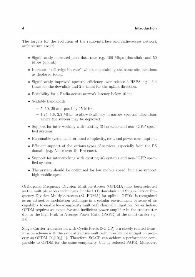
A generic radio transmitter consists of the baseband and Radio Frequency (RF)part, and both interactions are shown in Figure 1.4. The high spectral efficiencyrequirement can be achieved by performing a proper design of both advancedwireless techniques at the baseband level and the RF system architecture. TheLTE system level features, including advanced modulation and coding, MIMOantenna schemes and the interaction with higher layer protocol for link adapta-tion and packet scheduling, are implemented in the baseband. The RF systemdesign covers the investigation of the suitable RF architectures, detailed require-ments for each RF components, and the RF imperfections in the selected RFarchitectures.
Typically, each entity has its own evaluation metrics. The system level usesspectral efficiency performance, Block Error Rate (BLER), and cell-level capac-ity. In the RF design it is common to use moduation accuracy represented inthe Error Vector Magnitude (EVM), and the spectral regrowth aspects. It isalso very important to provide a link between these two entities. The evaluationmetric in the RF design can be further extended to analyze the impact of thehardware imperfections in the system level. Moreover, the RF requirements canbe determined from the system level requirement on the acceptable performance

8 Introduction
Baseband
Signal
Processings
RF
Transmitter
Spectral efficiency,
BER, BLER,
Cell capacity.
EVM,
Spectral emission,
ACLR.
Modulation,
Coding,
HARQ,
Radio Access,
MIMO, etc.
Nonlinear PA,
IQ imbalances,
Phase noise,
etc.
System Level Design RF Design
Figure 1.4: Hardware imperfections in the RF part limit the system level per-formance.
loss. In some cases, the RF requirement can be the main bottleneck of a wirelesscommunication system. Although the performance loss is still acceptable.
The RF imperfections occur in both transmitter and receiver. The RF imper-fections can lead to the performance degradation, and therefore it can limit theactual performance. In this work the RF imperfections are limited to the RFimperfections generated at the transmitter. Typically, the RF parts at the UEdominate the UE bill of material (BOM) cost. A low cost RF part will reducethe cost, and on the other hand the low performance component should also beexpected. Besides, the power amplifier is always the main consideration in thedesign of the RF transmitter. The main reason is that the good selection of apower amplifier results in an efficient power amplifier. The selection of the radioaccess scheme can also be decided due to the power amplifier characteristics. Aradio transmission with low peak-to-average power ratio is always preferred forthe uplink direction to obtain a better power amplifier efficiency.
Prior to the hardware implementation, the RF imperfections modelling andcomputer simulation offer some benefits in providing the results in term of linklevel performance degradation due to the hardware imperfections. Moreover,the result can be used as the reference for the actual hardware measurementresults in the latter stage.
Some work has been done in the RF imperfection modelling studies. Costa [13]analyzed the M-QAM-OFDM system performance in the presence of nonlinear

Hardware Imperfections: The Limiting Factor 9
power amplifier and phase noise. Georgiadis [14] provides analytical study onthe impact of gain, phase imbalance, and phase noise on EVM. These worksprovide the analysis in a limited scope and do not provide the relation betweenthe RF and system level requirements.
A consistent RF imperfection model is required for the wireless system standard-isation work (e.g: 3GPP) which cannot be based on a specific RF architecture.Nevertheless, it is also difficult to make the study completely independent of theRF architecture because some imperfections are specific to some RF architec-tures. For example, the gain and phase imbalance are produced in the Cartesiantransmitter architecture, and the envelope and phase timing alignment problemare in the Polar transmitter architecture.
The popular and commonly used RF architecture is the superheterodyne ar-chitecture and direct conversion architecture recently gained more popularity[15]. Each RF architecture has common components, such as local oscillator,mixer, filter, and amplifier. Those components have specific RF imperfections[16]. Furthermore, certain RF imperfections may occur in particular RF archi-tecture [16]. In this work the study of the impact of hardware imperfections isfacilitated by defining a behavioral model of each component. The behavioralmodel is obtained from the hardware measurement characteristics.
The relation between modulation format and power amplifier imperfection (non-linearity) plays an important role in the physical layer design stage, especiallyfor uplink transmission. The modulation format generally provides trade-offbetween bandwidth efficiency, power efficiency, and detectability [Raz99]. Thesethree parameters determine the capacity, the talk time, and the maximum range[raz99]. The uplink direction prefers a modulation format which has low PAPRand leads to a better talk time duration. It becomes critical for wide cell coveragein the cellular system.
An investigation on nonlinear power amplifier (PA) for the OFDM transmissionhas been carried out, and the non-linearity introduced a performance degrada-tion [17]. This is due to the high PAPR of the OFDM signals. The PAPR canbe reduced using several PAPR mitigation techniques [18]. However, there is adesign trade off between hardware complexity and system performance. Phasenoise in the local oscillator may degrade the performance, and it is known that amulti-carrier based system is more sensitive to the phase noise [13]. The effect ofphase noise in the LTE with channel estimation has also been investigated [19].The channel estimation is based on the pilot aided channel estimation (PACE)scheme.
Polar transmitter is considered as an alternative RF transmitter architectureaiming at a better power amplifier efficiency. Recently, it has been investigated
10 Introduction
for various wireless systems, such as EDGE, WCDMA, and OFDM wirelessLAN [20], [21], [22]. The main benefit is a high power amplifier efficiency atvarying power levels [23], and therefore it is suitable for a transmitter withvarying envelope signals. 3GPP LTE is one of the new wireless systems, whichhas a varying envelope signal since it uses DFT-spread OFDM modulation withvarious modulation schemes (BPSK, QPSK, and 16QAM). A polar transmitterhas numerous practical imperfections leading to spectral regrowth, increasedEVM, and link performance loss. One of the main challenges is that a polartransmitter requires high precision timing alignment between the envelope andphase path [24].
1.4 Objectives
The motivation of this PhD project is to design the uplink physical multiple-access for the upcoming B3G mobile communication system taking into accountthe combined constraints from system requirements and RF hardware imper-fections. The selection between single carrier and multi-carrier transmissionschemes are the bottom line in the design consideration since the multiple-access schemes mainly depend on the radio transmission techniques. Accordingto the best knowledge of the authors, no work has been done which provide acomprehensive result in relating the system level performance and RF require-ments.
The PhD research work is expected to result in the preferred multiple accesstechnique for the B3G system considering RF hardware imperfections and theRF transmitter requirements for the uplink direction. The work-scope can beillustrated in Figure 1.5. Physical layer parameter design, such as trade-off anal-ysis, methodology and guidelines for RF architecture including RF impairmentsmodel will be given. It is essential to consider both system requirements andRF hardware constraints to determine a feasible and realistic air interface forLTE uplink. The approach/methodology gathered in this project can also beapplied as the baseline in the design of uplink 4G system.
The PhD project has the following objectives:
1. Investigate the suitable air interfaces for the uplink transmission in Beyond3G (B3G) system.
2. Investigate the beyond 3G system performance using advanced modulation& coding, multiple-antennas, link adaptation, and H-ARQ techniques onspectral efficiency, cell coverage, and link quality of the uplink direction.

Scientific Methodology 11
B3G System
Parameters &
Requirements
Radio Access Technique:
Multi-Carrier
Single-CarrierRF Transmitter
Requirements
Figure 1.5: Work-scopes of the research project.
3. Identify and model the RF transmitter imperfections for the uplink direc-tion.
4. Identify the RF transceiver requirements suitable for the uplink in B3Gsystem.
5. Investigate the impact of the RF imperfections on the B3G uplink multi-user scenario that has a flexible transmission bandwidth.
6. Investigate the impact of the RF imperfections of the polar transmitter asthe candidate for the future RF Transmitter Architecture which offers ahigh efficient power amplifier.
7. Investigate the impact of inband inter-user interference on the uplink mul-tiple access of B3G system.
1.5 Scientific Methodology
This project considers the UTRA Long Term Evolution (LTE) system as asuitable system beyond 3G context to make the project results concrete andspecific. Design of multiple-access for LTE has the objective to achieve highspectral efficiency. However, some of the multiple access schemes are vulnerableto RF imperfections. The uplink includes handset transmitter and base-stationreceiver. Therefore, in the uplink direction that has limitations related to hand-set cost, size and power consumption, these limitations in combination withRF imperfections will most likely necessitate a different, or at least modified,

12 Introduction
physical access. Moreover, the many-to-one situation in the uplink require con-siderations on interference and power control related issues which are differentthan in the downlink direction.
Due to the complexity of the problem at hand the project makes extensive useof link simulations to observe the performance impact of different design choicesin the presence of RF and baseband hardware imperfections. For this purpose,detailed link simulation software has been developed with specific contributionsfrom this project on the RF hardware imperfections modelling. Analytical treat-ment is considered and is expected mainly to support the model developmentand confirm selected reference simulation results. The RF hardware architecturefor the uplink transmitter and receiver chain, and the corresponding RF hard-ware imperfection models, are analyzed separately and summarized in computersimulation models to be used in the detailed link layer simulations.
The results have been obtained through link level simulation and analytical stud-ies. A Monte Carlo link level simulation consists of a transmitter and receiverchain including a time dispersive channel model. The link level simulation con-sists of numerous advances techniques in wireless system to achieve high spectralefficiency [7]. The RF imperfection models have also been included to constructa practical simulator. The research methodology and obtained results are veri-fied through the theoretical analysis and the comparison with the other existingsimulation or measurement results.
The work of this project is divided in to two phases:
• The first phase provides the baseline results for the LTE uplink perfor-mance. A detailed study on the specific LTE uplink physical layer param-eter settings in both transmitter and receiver is performed to find out theoptimized settings. Most of the physical layer features, including variousantenna schemes, adaptive modulation and coding schemes, Hybrid-ARQ,link adaptation, are considered. The performance for both multiple accessschemes, OFDMA and SC-FDMA, are analyzed.
• The second phase is focused on the impact of RF transmitter hardwareimperfections and results in the RF transmitter requirement for LTE up-link. RF transmitter design will define the minimum requirement usingthe parameters and test cases specified in the standardization. B3G sys-tem has stringent requirement in order to achieve high spectral efficiency.Thus, it is a big challenge to design the RF transmitter part, such as defin-ing the RF architectures and RF component specifications. The key RFmeasurement parameters for the transmitter are the modulation accuracyor the Error Vector Magnitude (EVM), Spectrum Emission Mask (SEM)requirements, and Adjacent Channel Leakage Ratio (ACLR). Based on

Thesis Structure and Contributions 13
these key parameters, the RF transmitter requirements for the uplink inB3G system can be specified.
1.6 Thesis Structure and Contributions
This thesis consists of 8 chapters. The overview of each chapter is presentedand the contributions are highlighted in the bullet points.
Chapter 2 provides the background for the RF transmitter architectures, suchas cartesian and polar type architectures. The hardware imperfections on theRF transmitter architecture model and assumptions are also presented.
Chapter 3 presents the summary of LTE Uplink baseline performance results. Adetailed description on the developed link level simulator for LTE Uplink is madeand the link level simulator validation is given in Appendix. A. The results arefirstly given on the two main multiple-access schemes for the beyond 3G system,SC-FDMA and OFDMA. The impact of the new techniques in the beyond 3Gsystem, such as H-ARQ, antenna schemes, frequency allocation/diversity, toenhance the spectral efficiency is then given. The additional feature to increasethe performance by means of turbo equalization implementation at the receiveris discussed.
• Develop the UTRA LTE uplink link level simulator with most of L1 mainfunctionalities. Analysis of the LTE uplink performance in the ideal con-dition without the hardware imperfections. My major contributions arethe interleaver and de-interleaver, structuring the LTE uplink from thebaseline LTE downlink2, RF hardware imperfection model, and the turboequalization for the uplink3.
Chapter 4 summarizes the effect of RF imperfections on LTE Uplink perfor-mance. The Cartesian type architecture is assumed and the typical RF im-perfections for Cartesian architecture, such as nonlinear power amplifier, phasenoise, gain imbalance, phase imbalance and DC offset are considered.
• Provide the relation between individual RF imperfection EVM character-istics to the link level performance, especially to obtain a clear insight
2The LTE downlink was jointly developed together with the other PhD students: AkhileshPokhariyal, Na Wei, and Christian Rom.
3This study was undertaken in collaboration with the following research assistant: GilbertoBerardinelli.

14 Introduction
in the sensitivity on each RF impairment. The link level performanceis evaluated for AWGN and frequency selective fading channels. Perfor-mance evaluation in an AWGN channel represents the conditions underwhich EVM measurements are obtained for type approval, whereas theperformance evaluation in frequency selective fading is more representa-tive of actual operating conditions.
• Provide the relation between different RF transmitter impairment modelsin LTE uplink and how accurately the effect of each RF impairment can bemodelled by an equivalent white Gaussian noise source in the transmitter.
• Performance of SC-FDMA and OFDMA with the presence of nonlinearpower amplifier is evaluated.
Chapter 5 summarizes the RF transmitter design analysis on the spectrum emis-sion control aspect. The peak-to-average power ratio reduction is mainly thedesign strategy to increase the power amplifier efficiency, and the spectrum emis-sion control is to comply the transmit signal with the specification requirements.
• Propose and evaluate a spectrum shaping technique for LTE UE usingan Inverse Chebyshev Digital Infinite Impulse Response (IIR) filter. Thefilter selection is based on studies in [25] where this filter type achievesminimum capacity loss.
Chapter 6 discusses the alternative RF transmitter architecture solution basedon polar transmitter to achieve a high-efficiency power amplifier for LTE Uplink.The focus is on the impact of the polar transmitter imperfections, such as timingdelay alignment, non-linear amplifier and filter.
• Provide a link between individual RF imperfection EVM characteristicsto the link level performance, especially to obtain a clear insight of thesensitivity of each RF imperfection.
Chapter 7 discusses the In-band Inter-User Interference aspect on LTE Uplink.The scalable transmission bandwidth and flexible frequency allocation of theuser equipment, fractional power control, and RF imperfections leads the LTEuplink vulnerable to the inter-user interference.
• Propose and evaluate the power control parameters and the acceptableRF imperfections level to reduce the inter-user interference in the LTEuplink.

Publications 15
Finally, Chapter 8 presents the conclusions and the future work.
1.7 Publications
During the PhD studies, the following publications have been published:
1. B.E Priyanto, G. Berardinelli, T.B. Sørensen, ”Single Carrier Transmis-sion for UTRA LTE Uplink,” Long Term Evolution : 3GPP LTE Radioand Cellular Technology Handbook. Editor: Borko Furht, Syed A. Ahson.Boca Raton, Florida : CRC Press, April 2009.
2. B.E. Priyanto, T.B Sørensen, O.K. Jensen, ”In-Band Interference Effectson UTRA LTE Uplink Resource Block Allocation,” IEEE 67th VehicularTechnology Conference, Singapore, Singapore, May 2008.
3. B.E. Priyanto, T.B Sørensen, O.K. Jensen, T.E. Kolding, T. Larsen, P.Mogensen, ”A Spectrum Shaping Technique to Control Spectrum Emis-sion of UTRA LTE User Equipment,” IEEE Norchip 2007 Conf, Aalborg,Denmark, November. 2007.
4. B.E. Priyanto, T.B Sørensen, O.K. Jensen, T.E. Kolding, T. Larsen, P.Mogensen, ”Impact of Polar Transmitter Imperfections on UTRA LTEUplink Performance,” IEEE Norchip 2007 Conference, Aalborg, Denmark,November. 2007.
5. B.E. Priyanto, T.B Sørensen, O.K. Jensen, T.E. Kolding, T. Larsen, P.Mogensen ”Assessing and Modelling The Effect of RF Impairments onUTRA LTE Uplink Performance,” IEEE 66th Vehicular Technology Con-ference, Baltimore, United States, September 2007.
6. B.E. Priyanto, H. Codina, S.R. Simo, T.B Sørensen, P. Mogensen ”Ini-tial Performance Evaluation of DFT-Spread OFDM Based SC-FDMAfor UTRA LTE Uplink,” IEEE 65th Vehicular Technology Conference,Dublin, Ireland, April 2007.
7. B.E. Priyanto, C. Rom, , C.N. Manchon, T.B. Sørensen, P. Mogensen,O.K. Jensen, ”Effect of Phase Noise on Spectral Efficiency for UTRALong Term Evolution,” IEEE 17th International Symposium on PIMRC,Helsinki, Finland, September. 2006.
8. B.E. Priyanto, T.B Sørensen, O.K Jensen, ”On Investigation of Nonlin-ear Amplifier Distortion in OFDM Transmission,” IWS2005, InternationalWireless Summit 2005, Aalborg, Denmark, September 2005.
16 Introduction
Co-authored publications:
1. G. Berardinelli, B.E Priyanto, T.B. Sørensen, P.E. Mogensen, ”ImprovingSC-FDMA Performance by Turbo Equalizer in UTRA LTE Uplink,” IEEE67th Vehicular Technology Conference, Singapore, Singapore, May 2008.
2. N. Wei, A. Pokhariyal, C. Rom, B.E. Priyanto, F. Frederiksen, C. Rosa,T.B. Sørensen, T.E. Kolding, P. Mogensen, ”Baseline E-UTRA DownlinkSpectral Efficiency Evaluation,” IEEE 64th Vehicular Technology Confer-ence, Montreal, Canada, September 2006.
3. N. Behjou, B.E. Priyanto, O.K. Jensen, T. Larsen, ”Interference Issuesbetween UMTS & WLAN in a Multi-Standard RF Receiver,” IST MobileSummit Proceedings, Myconos, Greece, June 2006.
4. N. Behjou, B.E. Priyanto, O.K. Jensen, T. Larsen, ”RF Sub-System De-sign for Multi-Standard Digital-IF,” International Symposium on WirelessPersonal Multimedia Communcations, San Diego, United States, Septem-ber 2006.

“ No one is perfect... that’s why pencils have erasers.”
Anonymous
Chapter 2
RF Transmitter Architectures& Imperfections
2.1 Introduction
In a wireless communication system, a transmitter produces an RF signal forsending the information to the receiver over the air. The transmitter can trans-mit at a high power level to overcome path loss and maintain a high transmissionquality. Nevertheless, transmitting at high power can interfere other users sincethe transmission medium is shared among users. A power efficient transmitter isalso prefered, especially for a battery operated device to maintain long batterylife. Hence, there is a design trade-off in designing a transmitter.
A transmitter can be divided into two major parts: baseband and RF. Typ-ically, the baseband part is implemented digitally and the RF part is analog.A digital to analog converter (DAC) is placed in between and connecting thebaseband and RF part. The RF part for LTE has high requirements since it hasa specific target to deliver high speed transmission for both uplink and down-link. Moreover, the users have demand on a handy, stylish, and long batterylife user equipment [16]. Therefore, it is expected that the user equipment hasthe following target: keep minimizing the physical hardware size, efficient powerusage, and high performance transmitter with minimal RF imperfections.

18 RF Transmitter Architectures & Imperfections
An RF transmitter plays an important role in a transceiver and principally hasthree main functionalities: modulation, upconversion and power amplification.An RF transmitter consists of analog devices with high cost and with relativelyhigh power consumption. The RF transmitter design deals with the abovefunctionalities and aims to choose the proper block diagram/analog components.
The type of transmitted signal is also a main factor in an RF transmitter.It can be classified as the constant and non-constant envelope signals. An RFtransmitter gains advantage by processing a constant envelope signal because thesignal can be amplified by the power amplifier at high efficiency [26]. The non-constant envelope or variable envelope modulation has a large signal dynamicrange which can cause either a nonlinear distortion by the power amplifier ora low efficiency signal amplification. The 2nd generation of cellular systems,GSM and GPRS use a constant envelope signal, while the most recent systems,including LTE, use non-constant envelope signals.
The RF transmitter design results in various types of RF transmitter archi-tectures. The motivation is to adapt to the signal type from the baseband,increase the power efficiency, reduce the cost and possibly to support multi-mode operation. In general, the RF transmitter architectures can be dividedinto two major different types: Cartesian architectures and polar architectures.Each of those types can be divided in several transmitter architectures and haveadvantages/drawbacks which must be considered during the design phase.
The performance of the RF transmitter must be evaluated and follow the re-quirements defined by the relevant standard. The transmit signal should con-form with the transmit emission mask to ensure it does not interfere significantlywith other channels. The accuracy of the transmitted modulated signal shouldbe maintained high for reliable detection at the receiver and maintain high per-formance transmission. This is usually evaluated by the Error Vector Magnitude(EVM) parameter. Finally, a low power consumption is always preferred.
In this chapter, the overview of RF transmitter architectures on both cartesianand polar types is briefly introduced. A summary on the advantages and thedisadvantages of each architecture is given. The most common RF imperfec-tions in both cartesian and polar types are also elaborated, including the RFimperfections models. These models are later used in the study of the impactof RF imperfections.

Cartesian Transmitter Architectures 19
Baseband
Signal
Generator
DAC
DAC
LPF
LPF
0o/ 90o
IsolatorDuplexer
PA
DriverRF
VGA
UHF L.O
RF
Upconverter
IQ
Modulator
Tx
SAW
IF
VGA
VHF L.O
Figure 2.1: Cartesian superheterodyne RF transmitter architecture.
2.2 Cartesian Transmitter Architectures
Cartesian transmitter architectures fundamentally modulate the I&Q signalsfrom the baseband generator separately and then add them together to form anIF or RF signal. There are many types of RF transmitter architectures basedon the cartesian form, but one which is very popular is the superheterodynearchitecture. This architecture was invented in 1918 and still widely used untilnow. A block diagram of the superheterodyne architecture is shown in Figure2.1.
The I & Q baseband filtered analog input signals are mixed separately with anoffset local oscillator (LO) in a non-linear device (mixer) to produce intermediatefrequency (IF) signals. The LO signal for the Q channel is phase shifted by 90degree to provide orthogonality with the I channel. The mixing and combiningof I & Q channels are performed in the IQ modulator and produce a singleIF signal. The IF signal is then amplified by a variable gain amplifier (VGA).The amplified IF signal is up-converted to the RF frequency. The RF signal isfurther amplified by an RF VGA and then by a driver amplifier to a level that issufficient to drive the power amplifier (PA). Figure 2.1 shows that the variablegain control is located in both the IF and RF stage. The gain control in the IFis the crucial part since it dominates the overall gain control (around 75%) [15].
The commonly used PA is either a class AB or class C PA. Class AB is widelyused in the TDMA, CDMA, and wideband CDMA mobile phones [15]. Class Cis often employed in the GSM system [15]. An RF BPF filter is inserted betweenthe driver amplifier and PA to select the desired frequency band and suppress

20 RF Transmitter Architectures & Imperfections
out of band noise and unwanted mixing products generated by the up-converter.The PA gain and linearity performance can be affected by the load impedance.Thus, an isolator may be required at the PA output to reduce the effect ofantenna impedance variation [15]. This varying impedance problem is also verycommon in most other RF transmitter architectures. Finally, the duplexer hasthe primary task to reduce the transmitter signal leakage to the receiver and tosuppress the noise and spurious emission.
Most of the cellular systems are operating in Frequency Division Multiplexing(FDD) mode, where the uplink and downlink channels are assigned to two dif-ferents frequency band. Each frequency band consists of multi-channels andtypically each communication link occupies one channel. In this scenario, thefrequency planning in the superheterodyne architecture is very important. Thefrequency planning task is to find and select the IF frequency, which should min-imize the spurious response and should provide an excellent transceiver perfor-mance [15]. A superheterodyne transceiver may have the following fundamentalsignals:
• An RF local oscillator signal.
• A reference oscillator signal.
• Two or multiple RF signals.
• Two or multiple IF signals.
• A weak received RF signal.
• A high power transmitted signal.
The problem may occurs when there is a mixing products and harmonics inthe superheterodyne architecture due to the nonlinear components (LNA, highpower amplifier, and mixer). These potential issues are analyzed in the fre-quency planning stage[15]. In the frequency planning stage, potential problemsrelated to mioxing products and harmonics due to nonlinear components (LNA,power amplifier, and mixer) are investigated.
The advantages and the disadvantages of the superheterodyne RF transmitterarchitecture are shown in Table 2.1
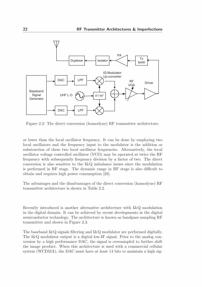
A solution to alleviate the superheterodyne RF transmitter is to employ a directconversion RF transmitter architecture. The direct conversion is also known asthe zero IF or homodyne architecture. The basic operation is a direct upconver-sion operation from the baseband to the RF signal without the IF stage. The

Cartesian Transmitter Architectures 21
Table 2.1: The superheterodyne architecture.
The advantages: The disadvantages:
• Widely used and a proventechnology since 1918.
• Implementation is quitestraightforward.
• Excellent performance in lin-earity.
• Requires a carefull design inthe frequency plan, especiallyfor a multi-mode user equip-ment.
• High component counts.
• High cost.
• Large size.
configuration of a direct conversion architecture is shown in Figure 2.2. Thedirect conversion is less complex than the superheterodyne since the number ofcomponents is reduced. At least, it eliminates the need for IF components, suchas filters, amplifiers, mixers, and local oscillator [27]. The benefit of the directconversion transmitter is not so attractive as the direct conversion receiver sincethere is no expensive IF channel filter saving at the transmitter [15].
As for the heterodyne transmitter, the baseband IQ signals from the digital toanalog converter (DAC) are filtered by low pass filters to suppress the adjacentchannel and eliminate aliasing products. The low pass filter can be implementedby an active LPF. Therefore, the bandwidth can be adjusted with the benefit tosupport multi-mode transmission. The IQ signals are then up-converted to RFand combined together by an IQ modulator. The RF output signal is amplifiedby an RF VGA and a driver amplifier so that the output signal can drive thepower amplifier. Most of the direct conversion transmitter gain (almost 90%) isgenerated in the RF stage [15]. An RF BPF is placed at the input of the PA tosuppress the out-of-band emission, leakage at the receiver band, and the noiseemission. An isolator and duplexer are also required for the direct conversiontransmitter.
Beside the advantages, the direct conversion transmitter suffers from the im-plementation issues, such as the injection pulling [16]. In a direct conversiontransmitter, the output signal and the local oscillator signal have the same fre-quency. The injection pulling occurs when the signal at the high power amplifieroutput is coupled back to the oscillator. The impact of the injection pulling canbe reduced if the high power amplifier output spectrum is sufficiently higher
22 RF Transmitter Architectures & Imperfections
Baseband
Signal
Generator
DAC
DAC
LPF
LPF
0o/ 90o
IsolatorDuplexer
PA
DriverRF
VGA
IQ Modulator
Up-converter
Tx
SAW
UHF L.O
Figure 2.2: The direct conversion (homodyne) RF transmitter architecture.
or lower than the local oscillator frequency. It can be done by employing twolocal oscillators and the frequency input to the modulator is the addition orsubstraction of these two local oscillator frequencies. Alternatively, the localoscillator voltage controlled oscillator (VCO) may be operated at twice the RFfrequency with subsequently frequency division by a factor of two. The directconversion is also sensitive to the I&Q imbalance issues since the modulationis performed in RF stage. The dynamic range in RF stage is also difficult toobtain and requires high power consumption [28].
The advantages and the disadvantages of the direct conversion (homodyne) RFtransmitter architecture is shown in Table 2.2.
Recently introduced is another alternative architecture with I&Q modulationin the digital domain. It can be achieved by recent developments in the digitalsemiconductor technology. The architecture is known as bandpass sampling RFtransmitter and shown in Figure 2.3.
The baseband I&Q signals filtering and I&Q modulator are performed digitally.The I&Q modulator output is a digital low-IF signal. Prior to the analog con-version by a high performance DAC, the signal is oversampled to further shiftthe image product. When this architecture is used with a commercial cellularsystem (WCDMA), the DAC must have at least 14 bits to maintain a high sig-

Cartesian Transmitter Architectures 23
Table 2.2: The direct conversion architecture.
The advantages: The disadvantages:
• Cost reduction by reducingthe number of components.
• Size reduction.
• Easy for multi-mode opera-tion.
• Does not need a frequencyplan.
• Much less spurious productsthan for the superheterodynetype [15].
• Problem with the injectionpulling.
• Problem with the I&Q imbal-ances issue.
• Difficulty to maintain high dy-namic range.
• Current consumption rela-tively high.
• Difficult for multi-band opera-tion.
nal to noise ratio output [15]. The analog output is connected to the RF BPFfilter with the task to select one of the spectral replicas of the signal centeredat the carrier frequency and suppress the other replicas and the out-of bandnoise. The bandwidth of the RF BPF filter is usually the frequency range of theintended application. The filter output is then amplified by the driver amplifierand a power amplifier. The transmitter signal dynamic range is controlled bythe PA gain control range, driver amplifier, and adjustable DAC voltage leveloutput [15].
The bandpass sampling RF transmitter architecture has the advantages and thedisadvantages as shown in Table 2.3.
From these three types of cartesian based architectures, it can be observed thefilters have three functionalities. First, the baseband lowpass filter to limitthe transmit signal in the channel bandwidth and shape the transmit signalspectrum. Second, the IF/RF bandpass filter to remove the unwanted outputafter the frequency conversion. Third, the bandpass filter in the duplexer is toprevent spurious and out of band emission [29].
24 RF Transmitter Architectures & Imperfections
Baseband
Signal
Generator
LPF
LPF
IsolatorDuplexer
PA Driver
DAC BPF
Tx sampling &
Clock Gen.
Figure 2.3: The bandpass sampling RF transmitter architecture.
Table 2.3: The bandpass sampling architecture.
The advantages: The disadvantages:
• Most of of the blocks can beimplemented in an integratedcircuit.
• Cost reduction.
• Size reduction.
• Some technical problems inthe direct conversion architec-ture can be solved.
• Requires a DAC with highsampling rate and a high dy-namic range.
• High power consumption, es-pecially at high sampling rateoperation.

Cartesian Transmitter Imperfections 25
2.3 Cartesian Transmitter Imperfections
In practice, the RF cartesian transmitter described in the previous section isaccompanied with the imperfections from the components. The basic compo-nents of an RF transmitter are analog filter, mixer, local oscillator and poweramplifier. The imperfections become more severe for a transmitter with the lowend (low cost) components. This section describes the most common RF trans-mitter imperfections, including nonlinear power amplifier, phase noise, gain andphase imbalances and DC offset. The generic imperfections models are alsogiven. These well-known models are used to facilitate the study on the impactof imperfections. The models of the imperfections are not dependent on thechoice of the architectures mentioned above.
2.3.1 Nonlinear Power Amplifier
The power amplifier amplifies the transmitted signal to ensure the receivedsignal has sufficient signal to noise ratio by compensating the path-loss betweentransmitter and receiver. One factor which must be highly considered is that thepower amplifier consumes a lot of power used in both handset and base-stationtransceivers. Therefore, achieving a highly efficient power amplifier is alwaysdesirable [30].
A power amplifier typically operates as a linear device for a small-signal. In-creasing the input power signal makes the power amplifier operate as a nonlineardevice and start to distort the transmitted signal. The distortion generates ad-ditional noise within the in-band channel and increase spectral regrowth in theadjacent channel. The linear and nonlinear operating region of a power amplifieris clearly defined by a saturation point of an amplifier. Within the linear region,a power amplifier provides a linear gain and at the saturation point the gain ofoutput signal is reduced by 1 dB. From this characteristic, the saturation pointis also known as 1 dB compression point. For simplicity, a power amplifier isassumed to be a time variant memoryless devices, and the nonlinearity effect ofa power amplifier on the transmitted signal is modeled as a power series [16]:
y(t) ≈ α1x(t) + α2x2(t) + α3x
3(t) (2.1)
The higher-order terms is known as harmonic distortion products. In (2.1), thenonlinearity effect of input signal with the power higher than 3 is neglected.
If a sinusoid signal x(t) = A cos ωt is the input signal, the output signal can be
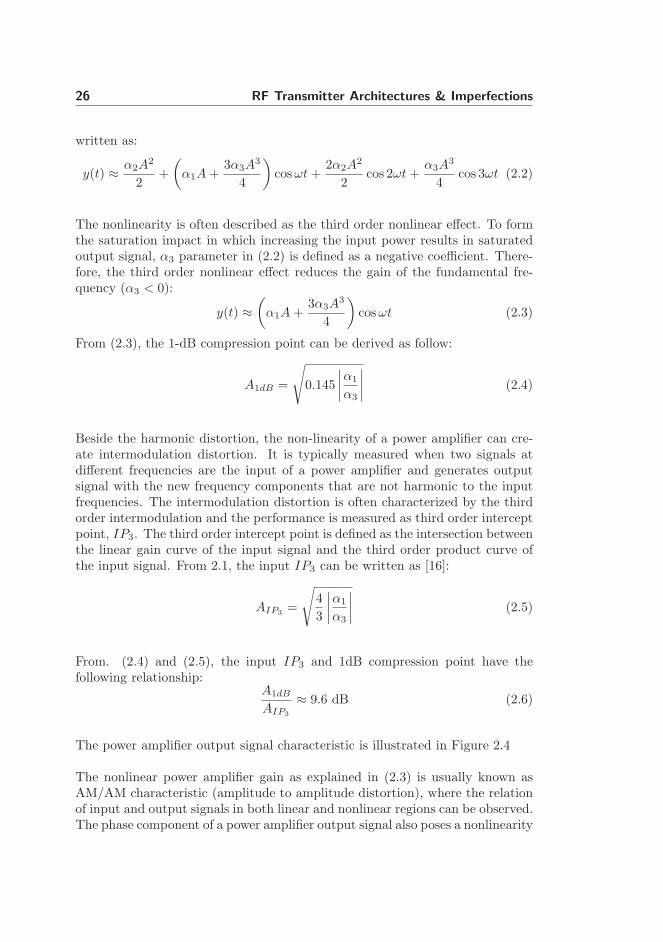
26 RF Transmitter Architectures & Imperfections
written as:
y(t) ≈ α2A2
2+
(α1A +
3α3A3
4
)cos ωt +
2α2A2
2cos 2ωt +
α3A3
4cos 3ωt (2.2)
The nonlinearity is often described as the third order nonlinear effect. To formthe saturation impact in which increasing the input power results in saturatedoutput signal, α3 parameter in (2.2) is defined as a negative coefficient. There-fore, the third order nonlinear effect reduces the gain of the fundamental fre-quency (α3 < 0):
y(t) ≈(
α1A +3α3A
3
4
)cos ωt (2.3)
From (2.3), the 1-dB compression point can be derived as follow:
A1dB =
√
0.145
∣∣∣∣α1
α3
∣∣∣∣ (2.4)
Beside the harmonic distortion, the non-linearity of a power amplifier can cre-ate intermodulation distortion. It is typically measured when two signals atdifferent frequencies are the input of a power amplifier and generates outputsignal with the new frequency components that are not harmonic to the inputfrequencies. The intermodulation distortion is often characterized by the thirdorder intermodulation and the performance is measured as third order interceptpoint, IP3. The third order intercept point is defined as the intersection betweenthe linear gain curve of the input signal and the third order product curve ofthe input signal. From 2.1, the input IP3 can be written as [16]:
AIP3=
√4
3
∣∣∣∣α1
α3
∣∣∣∣ (2.5)
From. (2.4) and (2.5), the input IP3 and 1dB compression point have thefollowing relationship:
A1dB
AIP3
≈ 9.6 dB (2.6)
The power amplifier output signal characteristic is illustrated in Figure 2.4
The nonlinear power amplifier gain as explained in (2.3) is usually known asAM/AM characteristic (amplitude to amplitude distortion), where the relationof input and output signals in both linear and nonlinear regions can be observed.The phase component of a power amplifier output signal also poses a nonlinearity

Cartesian Transmitter Imperfections 27
9.6 dB
1 dB
20log Ainput
20log Aout
AIP3A1dB
20log(3/4 A )a33
20log( A)a1
Figure 2.4: The power amplifier output signal characteristic.
28 RF Transmitter Architectures & Imperfections
effect and it is known as AM/PM characteristic (amplitude to phase distortion).The AM/PM has a similar behaviour as the AM/AM, when the input powersignal is increased, the phase output start to deviates. In practice, both AM/AMand AM/PM are characterized from a hardware measurement.
The performance of a power amplifier also includes to the efficiency factor. Thepower amplifier efficiency is usually defined as DC supply efficiency and poweradded efficiency (PAE). The power amplifier DC supply efficiency is expressedas follow [31]:
ηDC =Po
PDC(2.7)
where Po is the power amplifier ouput delivered to the antenna and PDC is theDC power in watts supplied to the power amplifier. PAE is a measure of thesignal power added by the power amplifier and it is expressed as follows [31]:
ηPAE =Po − Pi
PDC(2.8)
where Pi is the input signal power.
2.3.2 Gain & Phase Imbalances
An analog IQ modulator has a task to combine the I & Q channels to formthe IF or RF signal. A perfect I&Q modulator provides equal gain in the I&Qchannels and the Q channel is upconverted by a 90 degree phase shift relativeto the I channel. The practical I&Q modulator usually has imperfections andresults in imperfect match between the I & Q signals. The imperfections areknown as gain and phase imbalances. A gain imbalance makes the I channelbecomes slightly smaller than Q channel, or vice versa. The phase imbalancecauses the Q channel not to be shifted by exactly 90 degree with respect to the Ichannel. In practice, the amplitude imbalance is in the order of 1 dB and phaseimbalance below 5 degree [16].
The impact of gain and phase imbalance can be simply modeled using the base-band representation. The distorted modulator output signal is written as [32]:
y(t) = yI(t) + jyQ(t) (2.9)
yI(t) =
√2
1 + α2(xI(t) − αxQ(t)sin(θ)) (2.10)
yQ(t) =
√2
1 + α2(αxQ(t)cos(θ)) (2.11)
Cartesian Transmitter Imperfections 29
where α and θ are the gain imbalance and the phase imbalance parametersbetween the in-phase and quadrature channels, respectively. xI(t) and xQ(t)are the input signals to the I&Q modulator.
2.3.3 Phase Noise
The Phase noise can be described as the phase fluctuations due to the randomfrequency fluctuations of a local oscillator signal. A perfect local oscillatorgenerates a discrete single carrier frequency. However, due to the instability ofa local oscillator, it creates a random frequency around the center frequency ofa local oscillator. The performance of local oscillator is usually characterized bymeasuring the sideband noise of the output signal center frequency. The single-side band (SSB) phase noise is specified in dBc/Hz at a specified frequency offsetfrom the carrier frequency.
The phase noise can be modeled as a Wiener-Levy process [33]. This model isquite accurate to model a free-running oscillator and appropriate for quantitativestudies of system performance degradation due to phase noise [33]. The phasenoise effects can be seen as a multiplication of the transmitted signal with a noisycarrier ejΦ(t). The random phase of this carrier is modeled by a Wiener-Levyprocess as follows [13]:
Φ(t) = 2π
∫ t
0
µ (τ) dτ (2.12)
In (2.12), µ(t) is a zero-mean white Gaussian process with power spectral densityN0 . The resulting relative single-sideband (SSB) phase noise power spectraldensity follows a Lorentzian spectrum [13]:
L (f) =2
π∆f3dB.
1
1 +(
2f∆f3dB
)2 (2.13)
In (2.13), ∆f3dB = 2πN0 is the two-sided 3 dB bandwidth of phase noise. Thepower spectrum in (2.13) is an approximation to practical oscillator spectra,which enables analytical treatment.
The impact of the phase noise on the output signal can be simply modeled in abaseband representation [34]:
y (t) = x (t) · eφ(t) (2.14)

30 RF Transmitter Architectures & Imperfections
where x (t) is the input signal and φ (t) is time varying phase noise processgenerated by the local oscilator at the transmitter.
2.3.4 DC Offset
DC offset in the transmitter occurs because of the additional dc signal generatedin the baseband gain stage. The DC offset distorts the signal by shifting theIQ origin center of the signal constellation diagram. Thus, it causes a signalsaturation and bit error rate (BER) performance degradation [28]. The DCoffset is also known as the major problem in a direct conversion receiver.
The DC offset effect can be modeled using a discrete baseband model represen-tation and shown as [35]:
y(t) = yI(t) + jyQ(t) (2.15)
yI(t) = xI(t) + DCI (2.16)
yQ(n) = xQ(t) + DCQ (2.17)
where aI(t) and aQ(t) are the inphase and quadrature input signals, respectively.DCI and DCQ are the DC offset values in voltage. A similar problem is thelimited LO-RF leakage in the mixers in the modulator. The effect is the sameand is also covered by the model described.
2.3.5 DAC resolution and sampling rate
The digital to analog Converter (DAC) is the interface between the basebandand RF part. The DAC has several key parameters of which the most commonare the DAC number of bits and the sampling rate. A DAC with a highernumber of bits is prefered for a better performance because it can increase thesignal dynamic range and resolution. The usable dynamic range of a DAC isknown as spurious free dynamic range (SFDR) and illustrated in Figure 2.5.SFDR is the measure of the difference in amplitude between the fundamentaland largest harmonically or non-harmonically related spur from DC to the half
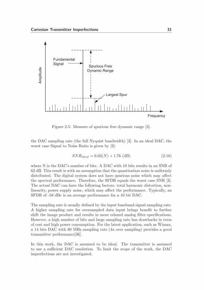
Cartesian Transmitter Imperfections 31
Fundamental
Signal
Frequency
Am
plit
ud
e
Spurious Free
Dynamic Range
Largest Spur
Figure 2.5: Measure of spurious free dynamic range [3].
the DAC sampling rate (the full Nyquist bandwidth) [3]. In an ideal DAC, theworst case Signal to Noise Ratio is given by [3]:
SNRideal = 6.02(N) + 1.76 (dB) (2.18)
where N is the DAC’s number of bits. A DAC with 10 bits results in an SNR of62 dB. This result is with an assumption that the quantization noise is uniformlydistributed. The digital system does not have spurious noise which may affectthe spectral performance. Therefore, the SFDR equals the worst case SNR [3].The actual DAC can have the following factors: total harmonic distortion, non-linearity, power supply noise, which may affect the performance. Typically, anSFDR of -58 dBc is an average performance for a 10 bit DAC.
The sampling rate is usually defined by the input baseband signal sampling rate.A higher sampling rate for oversampled data input brings benefit to furthershift the image product and results in more relaxed analog filter specifications.However, a high number of bits and large sampling rate has drawbacks in termof cost and high power consumption. For the latest application, such as Wimax,a 14 bits DAC with 80 MHz sampling rate (4x over sampling) provides a goodtransmitter performance[36].
In this work, the DAC is assumed to be ideal. The transmitter is assumedto use a sufficient DAC resolution. To limit the scope of the work, the DACimperfections are not investigated.

32 RF Transmitter Architectures & Imperfections
DAC
DAC
DAC
0o/ 90
o
PWMAM
LPF
Class E
PA
Class S PA
RF
Envelope tracker modulator
IQ ModulatorCartesian to Polar Converter
I(t)
Q(t) I(t)+Q(t)
I(t)+Q(t)
I(t)
I(t)+Q(t)
Q(t)
Figure 2.6: Polar EER transmitter architecture.
2.4 Polar Transmitter Architecture
The power amplifier efficiency is the main factor which may affect the wirelesstransceiver power consumption. There are many efforts in the RF transmitterarchitecture areas in order to increase the power amplifier efficiency [31], [26],[26]. Polar transmitter is one of RF transmitter architecture which offer a poweramplifier with a high efficiency.
The polar transmitter was initially invented by Kahn and named as EnvelopeElimination and Restoration (EER) transmitter [37]. Recently, it has been in-vestigated for various wireless system, such as EDGE, WCDMA, and OFDMwireless LAN [20],[22],[21]. The main benefit is a high power amplifier efficiencyat varying power levels [23] and therefore it is suitable for a transmitter withvarying envelope signals. A polar transmitter has numerous practical imperfec-tions leading to spectral regrowth, increase of Error Vector Magnitude (EVM)and link performance loss. One of the main challenges is that a polar transmit-ter requires a high precision timing alignment between the envelope and phasepath [24].
The polar transmitter structure is shown in Figure 2.6. The baseband signalgenerator output is up-sampled and filtered to further shift the image product.The original EER polar transmitter separates the analog envelope and phasepaths and processes them separately, and later restores the full signal at RF[37].Here, the separation, or the envelope elimination process, is performed digitally.The purpose is to avoid analog RF coupler, envelope detector and limiter whichtypically are used in the original EER polar transmitter.

Polar Transmitter Imperfections 33
The envelope polar signal is defined as:
A(t) =√
I(t)2 + Q(t)2 (2.19)
where I(t) and Q(t) are the Inphase and Quadrature signals, respectively. Sim-ilarly, the phase signal is defined via the two signals Iθ and Qθ:
Iθ(t) = cos(θ(t)) =I(t)
A(t)(2.20)
Qθ(t) = sin(θ(t)) =Q(t)
A(t)(2.21)
The nonlinear process results in a wider spectra of the output envelope signalcompared to the input I&Q signals [24]. For the WCDMA application, Resultsin [38] shows that at least a filter with the bandwidth of three times basebandbandwidth is required to meet WCDMA spectrum emission mask. The envelopesignal is amplified using a cascade of a pulse-width modulator (PWM), a switchmode class S amplifier, and a low pass filter (blocks inside the dashed box in Fig.2.6). The wide bandwidth envelope signal requires a high switching frequencywhich can result in reduced class-S PA efficiency [39]. In this work, the envelopesignal amplification is idealized. The phase path is up-converted to RF. It canbe done by an IQ modulator as shown in Fig. 2.6 or by a two-point-modulationphase locked-loop (PLL) [22]. The RF phase signal is then driving the PA andthe envelope is applied through the PA power supply.
2.5 Polar Transmitter Imperfections
A polar transmitter brings benefit for achieving a highly efficient power amplifierbut also suffers from several imperfections. The most common imperfections ina polar transmitter are described in the following section.
2.5.1 Timing Delay Alignment
After the envelope elimination process, the envelope and phase paths are treatedseparately prior to the signal restoration in the class E power amplifier. Theindividual paths can generate a timing delay alignment problem in the signalrestoration phase. The restored output signal phase, affected by the timingdelay, ∆t, in the phase path is defined as follows:
θ′(t) = θ(t + ∆t) (2.22)

34 RF Transmitter Architectures & Imperfections
2.5.2 Non-ideal PA
The AM/AM and AM/PM distortions always occur in the practical power am-plifier, especially when operating the signal at the maximum output power. Theoutput signal is also affected by a signal leakage from the phase path which showsup at low voltage levels [20]. The leakage is typically created due to capacitiveparasitic components.
A simple non-ideal PA model is included in Figure 2.7. The envelope path isdistorted by an AM/AM distortion. This distortion is modeled by a third ordernon-linearity which results in a signal amplitude given by:
A′(t) = A(t) + AM · A(t)3 (2.23)
where AM is the power level factor of the harmonic product relative to theaverage signal input power. The AM parameter is basically the coefficient ofthe third order component. The AM/PM conversion also distorts the outputsignal.
Measurement results on a class E PA suggest a linear phase deviation as afunction of input power level [20]. Here, the AM/PM is modeled by the linearslope PM to produce the signal phase:
θ′(t) = θ(t) + PM · A(t) (2.24)
The output signal is also affected by a signal leakage from the phase path whichshows up at low envelope levels. The leakage is typically created due to ca-pacitive parasitic components. Measurement results from [20] suggests that theleakage is modelled by the following additive phasor:
sL(t) = L · Re{
ejπ/2 · ejθ(t) · ejωCt}
(2.25)
where L is the power level factor of the leakage signal relative to the averageinput signal power, and e(jπ/2) is a constant phase offset of π/2.
Finally, the output signal affected by all of these imperfections is representedas:
s(t) = A′(t) · Re{
ej(θ(t+∆t)+PM ·A(t)) · ejωCt}
+ sL(t) (2.26)
where ωC is the RF carrier frequency.
The final model representing the timing delay alignment mismatch and the non-ideal PA is shown in Figure 2.7

Summary 35
A(t)+AM·A3(t)
PM
L
t
A(t)
ej( (t))
Dq
Figure 2.7: Imperfections model in a polar transmitter.
2.6 Summary
There are many RF transmitter architecture types and each of them has severaladvantages and disadvantages. Each architecture has its own RF imperfectionsconsideration. The DC offset becomes a crucial factor in a direct conversion, butnot for the other cartesian architecture family. The polar transmitter has a mainissue in dealing with timing delay alignment mismatch. Therefore, it is veryimportant to investigate the impact of those imperfections. The design challengeof the RF transmitter architecture is to supports a high transmission data rate,therefore it requires a high performance transmitter with small imperfections.The cartesian transmitter architecture still dominates and is widely used inthe existing wireless systems. The polar transmitter which offer better powerefficiency starts to be employed but comes along with many design challenges.It can be noticed that the power consumption still remains the main issue inthe RF transmitter architecture design. High power consumption can be dueto the high linearity power amplifier requirement or a high sampling rate of aDAC. The imperfections in each RF transmitter must be considered carefullyso that the system can achieve a high performance and meet the requirementdefined by the specification.

36 RF Transmitter Architectures & Imperfections
“ Proper preparation prevents poorperformance.”
Charlie Batch
Chapter 3
Baseline LTE UplinkPerformance Analysis
3.1 Introduction
LTE uplink transmission has numerous recent physical layer considerations incomparison to the UTRA WCDMA system, mainly to achieve 2-3 times betterspectral efficiency. These advances include a flexible channel bandwidth up to 20MHz, flexible user resource blocks allocation in both time and frequency domain,and a shorter time transmission interval (TTI) of 1 ms. Specifically challengingfor the uplink is that these enhancements are to be achieved, preferably, withreduced power consumption to extend the battery life and/or increase the cellcoverage.
The radio access technique is one of the key issues in the LTE uplink air inter-face. In LTE, Orthogonal Frequency Division Multiple-Access (OFDMA) hasbeen selected as the multiple access scheme for downlink and Single-CarrierFrequency Division Multiple-Access (SC-FDMA) for uplink. OFDM is an at-tractive modulation technique in a cellular environment to combat frequencyselective fading channel with a relatively low-complexity receiver [40]. How-ever, OFDM requires an expensive and inherently inefficient power amplifier inthe transmitter due to the high Peak-to-Average Power Ratio (PAPR) of the

38 Baseline LTE Uplink Performance Analysis
multi-carrier signal.
Single Carrier transmission with Cyclic Prefix (SC-CP) is an alternative trans-mission scheme with the same attractive multipath interference mitigation prop-erty as OFDM [9, 10, 11]. Therefore, SC-CP can achieve a link level performancecomparable to OFDM for the same complexity, but at reduced PAPR [9]. Inaddition, the performance of SC-CP can be further improved by using a turboequalization receiver [41]. The choice of single carrier transmission in a DFT-Spread OFDM form allows for a relatively high degree of commonality with thedownlink OFDM scheme and the possibility to use the same system parame-ters [5]. Moreover, it enables a direct access to frequency domain to performfrequency domain equalization [9].
The aim of this work is to assess the LTE uplink performance and provide thebaseline results in ideal condition without the RF imperfection. The impact andsignificance of the key techniques in LTE uplink are evaluated. The baseline per-formance evaluation is based on the two candidates for beyond 3G radio accesstechnique which are OFDMA and SC-FDMA. OFDMA is evaluated becauseit is still a candidate for the other beyond 3G uplink system, such as Wimaxand, later both performance can be assessed. The baseline results are usedas the reference for the subsequent study in dealing with the RF transmitterimperfections.
This chapter is organized as follows. LTE uplink numerology is introduced inSection 3.2. The description of both radio access techniques is given in Section3.3. LTE uplink transmitter & receiver model used in this study is given inSection 3.4. The peak-to-average power ratio (PAPR) evaluation for each radioaccess scheme is discussed in Section 3.5. Frequency domain equalization in LTEuplink receiver is discussed in Section 3.6, including both minimum mean-squareerror (MMSE) and zero forcing (ZF) techniques. Afterwards, the LTE uplinkperformance with various key techniques is presented, including fast H-ARQ inSection 3.8, link adaptation in Section 3.7, antenna configuration in Section 3.9,flexible frequency allocation in Section 3.10. Channel estimation with wienerfilter is given in Section 3.11. Turbo equalizer, as a performance enhancementtechnique for SC-FDMA transmission, is presented in Section 3.12. Finally, asummary is given in Section 3.13.
3.2 LTE Uplink Numerology
The basic physical layer parameters that were originally designed for the up-link are shown in Table 3.1 [5]. The transmission scheme is SC-FDMA in a

LTE Uplink Numerology 39
DFT-spread OFDM form. Different transmission bandwidths have different pa-rameter settings. The transmission is frame based with a radio frame durationof 10 ms and consists of 20 sub-frames of 0.5 ms. A sub-frame is equivalent to atransmission time interval (TTI). The sub-frame structure for uplink transmis-sion is shown in Figure 3.1.
C
PLB#1
C
P
SB#
1
C
PLB#2
C
PLB#3
C
PLB#4
C
PLB#5
C
P
SB#
2
C
PLB#6
0.5 ms
Figure 3.1: LTE uplink sub-frame structure with 2 short blocks.
Based on [5], a sub-frame consists of two short blocks and six long blocks. Theshort-block is a reference symbol and transmitted in a time-multiplex formatwith the long-block. It has the following purposes:
• Uplink channel estimation for uplink coherent demodulation/detection
• Possible uplink channel quality estimation for uplink frequency and/ortime-domain channel dependent scheduling
The short block duration is half the long block duration. The long block isprimarily used to transmit data.
In the work item phase, 3GPP has modified certain physical layer parameters,and hence has changed the assumptions that were initially applied for the eval-uations. In particular, the sub-frame/TTI duration has changed to 1 ms toinclude two 0.5 ms slots, each with a structure as shown in Figure 3.2. Themodified short blok duration is equal to the long block. At the writing of thisdissertation, the position of the modified short block has not been finalized. InFigure 3.2, the modified short block is located in the middle of the slot. Initially,the supported modulation schemes are π/2 BPSK, QPSK, 8PSK, and 16QAM.In the work item phase, the supported modulation scheme for data transmissionwas changed in the work item phase to QPSK, 16QAM, and 64QAM (optional).
C
PLB#1
C
PLB#2
C
PLB#3
C
PLB#4
C
PLB#5
C
PLB#6
0.5 ms
CP SB#1
Figure 3.2: LTE uplink slot structure with 1 short block.
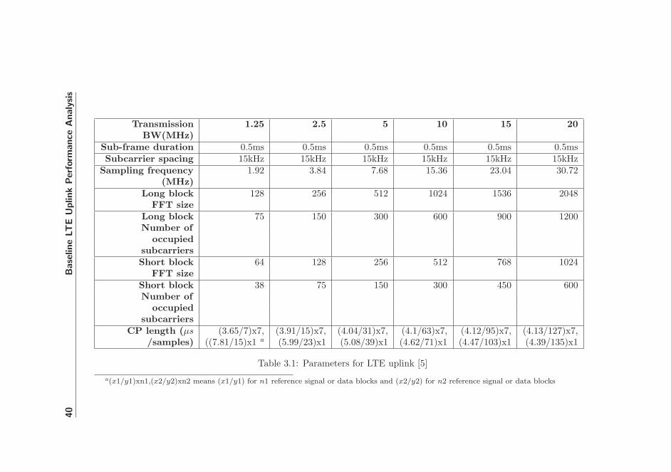
40
Base
line
LTE
Uplink
Perform
ance
Analy
sis
Transmission 1.25 2.5 5 10 15 20BW(MHz)
Sub-frame duration 0.5ms 0.5ms 0.5ms 0.5ms 0.5ms 0.5msSubcarrier spacing 15kHz 15kHz 15kHz 15kHz 15kHz 15kHz
Sampling frequency 1.92 3.84 7.68 15.36 23.04 30.72(MHz)
Long block 128 256 512 1024 1536 2048FFT size
Long block 75 150 300 600 900 1200Number of
occupiedsubcarriersShort block 64 128 256 512 768 1024
FFT sizeShort block 38 75 150 300 450 600Number of
occupiedsubcarriers
CP length (µs (3.65/7)x7, (3.91/15)x7, (4.04/31)x7, (4.1/63)x7, (4.12/95)x7, (4.13/127)x7,/samples) ((7.81/15)x1 a (5.99/23)x1 (5.08/39)x1 (4.62/71)x1 (4.47/103)x1 (4.39/135)x1
Table 3.1: Parameters for LTE uplink [5]
a(x1/y1)xn1,(x2/y2)xn2 means (x1/y1) for n1 reference signal or data blocks and (x2/y2) for n2 reference signal or data blocks
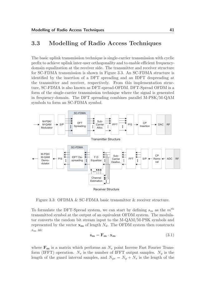
Modelling of Radio Access Techniques 41
3.3 Modelling of Radio Access Techniques
The basic uplink transmission technique is single-carrier transmission with cyclicprefix to achieve uplink inter-user orthogonality and to enable efficient frequency-domain equalization at the receiver side. The transmitter and receiver structurefor SC-FDMA transmission is shown in Figure 3.3. An SC-FDMA structure isidentified by the insertion of a DFT spreading and an IDFT despreading atthe transmitter and receiver, respectively. From this implementation struc-ture, SC-FDMA is also known as DFT-spread-OFDM. DFT-Spread OFDM is aform of the single-carrier transmission technique where the signal is generatedin frequency-domain. The DFT spreading combines parallel M-PSK/M-QAMsymbols to form an SC-FDMA symbol.
M-PSK/
M-QAM
Modulator
S/PDFT
SpreadingIFFT
CP
InsertionP/S
M-PSK/
M-QAM
Demo-
dulator
P/SIDFT De-
spreadingFFT
CP
Remo
val
S/PF.D
Equalizer
Channel
Estimation
DAC RF
ADC RF
Transmitter Structure
Receiver Structure
SC-FDMA
SC-FDMA
Sub-
Carrier
Alloc.
Sub-
Carrier
Dealloc.
Figure 3.3: OFDMA & SC-FDMA basic transmitter & receiver structure.
To formulate the DFT-Spread system, we can start by defining sm as the mth
transmitted symbol at the output of an equivalent OFDM system. The modula-tor converts the random bit stream input to the M-QAM/M-PSK symbols andrepresented by the vector xm of length Nd. The OFDM system then constructssm as:
sm = Fm · xm (3.1)
where Fm is a matrix which performs an Ns point Inverse Fast Fourier Trans-form (IFFT) operation. Ns is the number of IFFT output samples. Ng is thelength of the guard interval samples, and Ngs = Ng + Ns is the length of the

42 Baseline LTE Uplink Performance Analysis
Dm =
Dm,0 [0] · · · Dm,Nd−1 [0]. . .
... Dm,k [n]...
. . .
Dm,0 [Nd − 1] · · · Dm,Nd−1 [Nd − 1]
(3.3)
total time domain symbol.
The mth transmitted symbol in a DFT-S OFDM system can be expressed as avector of length Ngs samples, defined by:
sm = Fm · Tm · Dm · xm (3.2)
Dm is a matrix which performs an Nd points Discrete Fourier Transform (DFT)operation. The DFT spreading matrix element is expressed as:
Dm,k [n] =1√Nd
.e−j2πk
(n
Nd
)
(3.4)
where k is the M-QAM/PSK symbol index. Tm is a Ns × Nd mapping matrixfor the subcarrier allocation. The subcarrier allocation can be classified in twoallocation modes, namely distributed and localized allocation [5] (See also Figure3.18). In distributed mode, Ns = Sf ·Nd with Sf defined as the spreading factor.The matrix of subcarrier allocation in localized mode is defined as:
Tm = [0q×Sf ,1JNd,10Ns−Nd−q×Sf;0Ns,Nd−1] (3.5)
Where q is the localized chunk index. Ja,b is an a × b matrix of ones. For thedistributed mode, the sub-carrier allocation matrix is defined as:
Tm = [J1,10Sf−1,1 · · · JNd,10Sf−1,1;0Ns,Nd−1] (3.6)
Finally, Fm has matrix element given by:
Fm,l [n] =1√Ns
.ej2πl
(n−Ng
Ns
)
(3.8)
where l is the subcarrier index.

Modelling of Radio Access Techniques 43
Fm =
Fm,0 [0] · · · Fm,Ns−1 [0]. . .
... Fm,l [n]...
. . .
Fm,0 [Ngs − 1] · · · Fm,Ns−1 [Ngs − 1]
(3.7)
After the multipath channel and adding the additive white gaussian noise (AWGN),removing the cyclic prefix and going through the N points FFT, the receivedsignal vector in the frequency domain can be expressed as:
zm = Hm · Tm · Dm · xm + wm (3.9)
where Hm is the diagonal matrix of channel response, and wm is the noisevector. In this system, the maximum excess delay of the channel is assumedto be shorter than the cyclic prefix duration and, therefore, the inter-symbolinterference (ISI) can easily be eliminated by removing the cyclic prefix.
The linear amplitude and phase distortion in the received signal as a result ofthe multipath channel is compensated by a frequency domain equalizer (FDE).After FDE, the output signal is:
Vm = Cm · zm (3.10)
where Cm is the matrix diagonal of FDE coefficients:
Cm = diag(Cm,1,Cm,2, . . . ,Cm,Nd) (3.11)
The FDE coefficients generation is described in Section 3.6.

44 Baseline LTE Uplink Performance Analysis
3.4 Modeling and Validation of LTE uplink Trans-mitter & Receiver
A model of the Layer-1 (L-1) LTE uplink transmitter and receiver structures isshown in Figure 3.4. The left side is the transmitter, corresponding to the userequipment (UE), and the right side is the receiver, corresponding to the node-Bor base-station (BS). Several throughput enhancement mechanisms are imple-mented, including turbo coding, adaptive modulation coding (AMC) based onlink adaptation (LA) and Hybrid ARQ (HARQ) based on fast L1 retransmis-sions. The detailed descriptions are provided in Appendix A.1. The validationof the transmitter and receiver chain is described in Appendix A.2.
3.5 Peak-to-Average Power Ratio Evaluation
The envelope variation of the transmitted signal can be represented in a peak-to-average power ratio parameter (PAPR). In this work, the PAPR of bothSC-FDMA and OFDMA is evaluated. The PAPR is an essential parameterwhich can affect the RF part, since a transmitter signal with high PAPR issensitive to the non-linear distortion at the power amplifier. The PAPR of thetransmitted signal can be expressed as:
CCDF (Pins) = Prob
{|vi|2Pavg
> PT
}(3.12)
where Pins is the instantaneous power of the signal, vi is the ith signal samples,Pavg is the long term average power, and PT is the power threshold of the signal.For simplicity, Pavg has been normalized to one. In order to obtain accurateresults, the transmitted signal has been oversampled 4 times according to thesuggestion given in [18].
Figure 3.5 shows the PAPR results for SC-FDMA with various modulationschemes. The PAPR results vary depending on the modulation scheme so thathigher order modulation schemes exhibits a higher PAPR compared to lowerorder modulation schemes. In SC-FDMA, as a single carrier transmission, thePAPR is mainly affected by the envelope variations in each modulation scheme,thus the higher order modulations lead to larger dynamic range and higherPAPR. The same results are also shown in [42].
In comparison, the PAPR results for OFDMA with various modulation schemes

Peak-to-Average Power Ratio Evaluation 45
Transport block
generator
CRC attachment
Code block
segmentation
Channel Coding
L1-HARQ & Rate
Matching
Interleaver
QAM/PSK
Constellation
Mapping
DFT-Spreading
Sub-carrier Mapping
IFFT & CP Insertion
BER & BLER
Measurement
CRC verifications
Code block
desegmentation
Channel Decoding
L1-HARQ & de-Rate
Matching
Deinterleaver
QAM/PSK
Constellation
Demapping
IDFT-Despreading
FFT & CP removal
Multipath
Channel
UE Base stationInput
from LA
MMSE
Equalizer
Sub-carrier
Demapping
Figure 3.4: Layer-1 UTRA LTE uplink link level simulator

46 Baseline LTE Uplink Performance Analysis
0 1 2 3 4 5 6 7 8 910
−6
10−5
10−4
10−3
10−2
10−1
100
PT (dB)
CC
DF
(P
ins)
pi/2 BPSKQPSK8PSK16QAM64QAM
Figure 3.5: PAPR of SC-FDMA with various modulation schemes.
0 2 4 6 8 10 12 1410
−7
10−6
10−5
10−4
10−3
10−2
10−1
100
PT (dB)
CC
DF
(P
ins)
pi/2 BPSKQPSK8PSK16QAM64QAM
Figure 3.6: PAPR of OFDM for various modulation schemes.
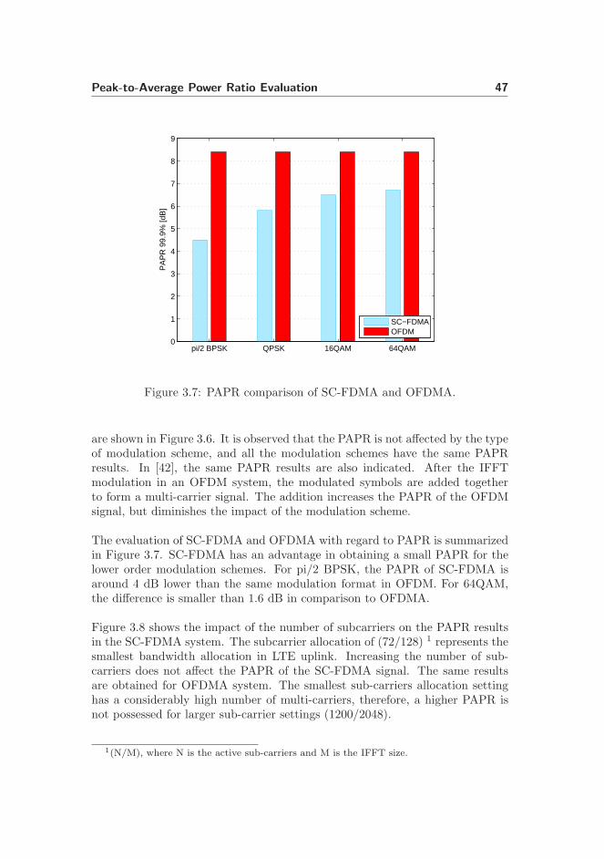
Peak-to-Average Power Ratio Evaluation 47
pi/2 BPSK QPSK 16QAM 64QAM0
1
2
3
4
5
6
7
8
9
PA
PR
99.
9% [d
B]
SC−FDMAOFDM
Figure 3.7: PAPR comparison of SC-FDMA and OFDMA.
are shown in Figure 3.6. It is observed that the PAPR is not affected by the typeof modulation scheme, and all the modulation schemes have the same PAPRresults. In [42], the same PAPR results are also indicated. After the IFFTmodulation in an OFDM system, the modulated symbols are added togetherto form a multi-carrier signal. The addition increases the PAPR of the OFDMsignal, but diminishes the impact of the modulation scheme.
The evaluation of SC-FDMA and OFDMA with regard to PAPR is summarizedin Figure 3.7. SC-FDMA has an advantage in obtaining a small PAPR for thelower order modulation schemes. For pi/2 BPSK, the PAPR of SC-FDMA isaround 4 dB lower than the same modulation format in OFDM. For 64QAM,the difference is smaller than 1.6 dB in comparison to OFDMA.
Figure 3.8 shows the impact of the number of subcarriers on the PAPR resultsin the SC-FDMA system. The subcarrier allocation of (72/128) 1 represents thesmallest bandwidth allocation in LTE uplink. Increasing the number of sub-carriers does not affect the PAPR of the SC-FDMA signal. The same resultsare obtained for OFDMA system. The smallest sub-carriers allocation settinghas a considerably high number of multi-carriers, therefore, a higher PAPR isnot possessed for larger sub-carrier settings (1200/2048).
1(N/M), where N is the active sub-carriers and M is the IFFT size.
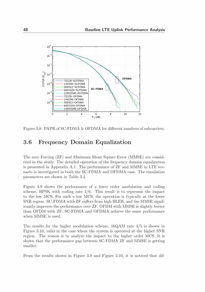
48 Baseline LTE Uplink Performance Analysis
0 2 4 6 8 10 12
10−6
10−5
10−4
10−3
10−2
10−1
100
PT (dB)
CC
FD
F (
Pin
s)
72/128−SCFDMA144/256−SCFDMA300/512−SCFDMA600/1024−SCFDMA1200/2048−SCFDMA72/128−OFDMA144/256−OFDMA300/512−OFDMA600/1024−OFDMA1200/2048−OFDMA
OFDMA
SC−FDMA
Figure 3.8: PAPR of SC-FDMA & OFDMA for different numbers of subcarriers.
3.6 Frequency Domain Equalization
The zero Forcing (ZF) and Minimum Mean Square Error (MMSE) are consid-ered in the study. The detailed operation of the frequency domain equalizationis presented in Appendix A.1. The performance of ZF and MMSE in LTE sce-nario is investigated in both the SC-FDMA and OFDMA case. The simulationparameters are shown in Table 3.2.
Figure 3.9 shows the performance of a lower order modulation and codingscheme, BPSK with coding rate 1/6. This result is to represent the impactto the low MCS. For such a low MCS, the operation is typically at the lowerSNR region. SC-FDMA with ZF suffers from high BLER, and the MMSE signif-icantly improves the performance over ZF. OFDM with MMSE is slightly betterthan OFDM with ZF. SC-FDMA and OFDMA achieve the same performancewhen MMSE is used.
The results for the higher modulation scheme, 16QAM rate 4/5 is shown inFigure 3.10, valid in the case where the system is operated at the higher SNRregion. The reason is to analyze the impact to the higher order MCS. It isshown that the performance gap between SC-FDMA ZF and MMSE is gettingsmaller.
From the results shown in Figure 3.9 and Figure 3.10, it is noticed that dif-
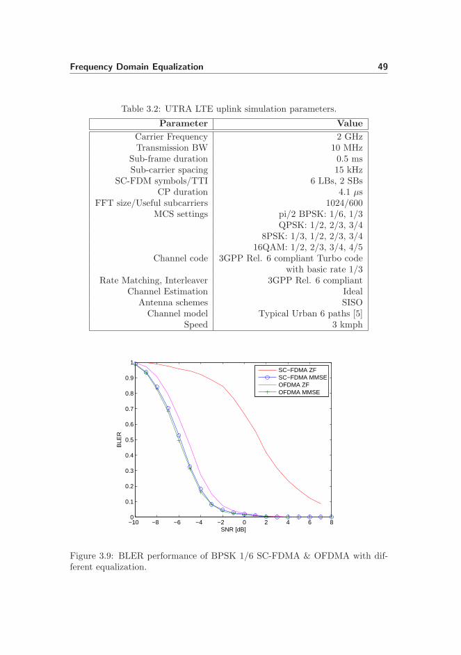
Frequency Domain Equalization 49
Table 3.2: UTRA LTE uplink simulation parameters.
Parameter Value
Carrier Frequency 2 GHzTransmission BW 10 MHz
Sub-frame duration 0.5 msSub-carrier spacing 15 kHz
SC-FDM symbols/TTI 6 LBs, 2 SBsCP duration 4.1 µs
FFT size/Useful subcarriers 1024/600MCS settings pi/2 BPSK: 1/6, 1/3
QPSK: 1/2, 2/3, 3/48PSK: 1/3, 1/2, 2/3, 3/4
16QAM: 1/2, 2/3, 3/4, 4/5Channel code 3GPP Rel. 6 compliant Turbo code
with basic rate 1/3Rate Matching, Interleaver 3GPP Rel. 6 compliant
Channel Estimation IdealAntenna schemes SISO
Channel model Typical Urban 6 paths [5]Speed 3 kmph
−10 −8 −6 −4 −2 0 2 4 6 80
0.1
0.2
0.3
0.4
0.5
0.6
0.7
0.8
0.9
1
SNR [dB]
BLE
R
SC−FDMA ZFSC−FDMA MMSEOFDMA ZFOFDMA MMSE
Figure 3.9: BLER performance of BPSK 1/6 SC-FDMA & OFDMA with dif-ferent equalization.

50 Baseline LTE Uplink Performance Analysis
8 10 12 14 16 18 20 22 24 260
0.1
0.2
0.3
0.4
0.5
0.6
0.7
0.8
0.9
1
SNR [dB]
BLE
R
SC−FDMA ZFSC−FDMA MMSEOFDMA ZFOFDMA MMSE
Figure 3.10: BLER performance of 16QAM 4/5 SC-FDMA & OFDMA withdifferent equalization.
ferent equalization technique does not affect significantly the OFDM system.However, it becomes a critical issue for SC-FDMA. Forward Error Correctioncode used in this analyzes is the turbo code [12]. In OFDM transmission, theFEC provides an important role to provide additional diversity, especially forthe transmission over frequency selective fading. While in SC-FDMA, the FECis also still important, but it does not provide additional diversity since it hasthe DFT-spreading.
Figure 3.11 and Figure 3.12 show the SC-FDMA spectral efficiency resultsin both MMSE and ZF. The spectral efficiency which can also be called thethroughput is calculated using:
TP =(1 − BLER) ∗ P
T ∗ B(3.13)
Where BLER is the Block Error Rate, P is the subframe (block) size, T is thesubframe duration, and B is the bandwidth. The results are also presented forall modulation schemes suitable for LTE uplink. MMSE is significantly betterthan ZF, especially in low SNR range. SC-FDMA with ZF suffers from noiseenhancement. It is clearly shown that the SC-FDMA MMSE is always preferredto ZF in all simulated conditions.

Frequency Domain Equalization 51
−10 −5 0 5 10 15 20 250
0.5
1
1.5
2
2.5
3
SNR [dB]
Spe
ctra
l Effi
cien
cy [b
/s/H
z]
pi/2 BPSK 1/6pi/2 BPSK 1/3QPSK 1/2QPSK 2/3QPSK 3/48PSK 1/38PSK 3/416QAM 1/216QAM 2/316QAM 3/416QAM 4/5
Figure 3.11: Spectral efficiency of SC-FDMA with Zero Forcing equalization.
−10 −5 0 5 10 15 20 250
0.5
1
1.5
2
2.5
3
SNR [dB]
Spe
ctra
l Effi
cien
cy [b
/s/H
z]
pi/2 BPSK 1/6pi/2 BPSK 1/3QPSK 1/2QPSK 2/3QPSK 3/48PSK 1/38PSK 3/416QAM 1/216QAM 2/316QAM 3/416QAM 4/5
Figure 3.12: Spectral efficiency of SC-FDMA with MMSE equalization.

52 Baseline LTE Uplink Performance Analysis
3.7 Impact of Link Adaptation
In this study, a simple link adaptation technique is adopted in which the linkadaptation is defined as a maximum achievable throughput/spectral efficiencyfor various modulations and coding schemes. The selection of modulation andcoding scheme is based on average signal to noise ratio (SNR). The measuredSNR at the base station, represented as Channel State Information (CSI), variesdepending on the channel condition. Here the CSI measurement is assumedideal, whereas in practise it will be influence by measurement inaccuracy andquantization noise.
The spectral efficiency of different MCS in SISO case without HARQ is plottedversus the average SNR in Figure 3.13. Variable rate turbo encoding and modu-lation from pi/2 BPSK to 16QAM provide peak data rates from 1.2 Mbps up to23 Mbps for the system with 10 MHz bandwidth. In these peak data rates, the14% pilot overhead described in Section 3.2 has been taken into account. Theused MCS formats and corresponding data rate values are summarized in Table3.3. It can be observed that 8PSK does not contribute to the link adaptationcurve.
−10 −5 0 5 10 15 20 25 300
0.5
1
1.5
2
2.5
SNR (dB)
Spe
ctra
l effi
cien
cy (
b/se
c/H
z)
pi/2 BPSK 1/6 pi/2 BPSK 1/3 QPSK 1/2 QPSK 2/3 QPSK 3/4 8PSK 1/3 8PSK 1/2 8PSK 2/3 8PSK 3/4 16QAM 1/2 16QAM 2/3 16QAM 3/4 16QAM 4/5 Link adaptation
Figure 3.13: Spectral efficiency of SISO SC-FDMA with various MCS schemes.

Impact of Fast HARQ 53
Table 3.3: Peak Data Rate For 10 MHz System
MCS Data Rate
pi/2 BPSK 1/6 1.2 Mbps
pi/2 BPSK 1/3 2.4 Mbps
QPSK 1/2 8PSK 1/3 7.2 Mbps
QPSK 2/3, 9.6 Mbps
QPSK 3/4, 8PSK 1/2 10.8 Mbps
16QAM 1/2, 8PSK 2/3 14.4 Mbps
8PSK 3/4 16.2 Mbps
16QAM 2/3 19.2 Mbps
16QAM 3/4 21.6 Mbps
16QAM 4/5 23 Mbps
3.8 Impact of Fast HARQ
A fast L1 Hybrid ARQ (HARQ) retransmission concept is used with the aimof facilitating a more aggresive and spectrally efficient packet scheduling [43].Two soft combining HARQ retransmission mechanisms are considered, namelychase combining and incremental redundancy. Both retransmission mechanismsensure that the past retransmission is fully utilized. The major difference be-tween these two retransmission mechanisms is that chase combining requiresthe same transmitted signal in each retransmission, whereas incremental redun-dancy transmits different parity bits in each retransmission.
The HARQ within the MAC sublayer has the following characteristics:
• N-process Stop-And-Wait (SAW) HARQ is used; The HARQ processes aretransmitted over N parallel time channels in order to ensure the continuoustransmission to the UE.
• The HARQ is based on ACK/NACKs; The received data packets areacknowledged after each transmission. A negative ACK (NACK) impliesa retransmission request either for an additional redundancy for HARQincremental redundancy or an identical packet for HARQ chase combiningcase.
• For the uplink, the HARQ is based on synchronous retransmissions.

54 Baseline LTE Uplink Performance Analysis
0 5 10 15 20 25 300
0.5
1
1.5
2
2.5
3
SNR (dB)
Spe
ctra
l effi
cien
cy (
b/se
c/H
z)
16QAM 1/2 Chase Combining16QAM 1/2 Incr. Redundancy16QAM 4/5 Chase Combining16QAM 4/5 Incr. Redudancy
Figure 3.14: Spectral efficiency of SC-FDMA SISO case for chase combining(CC) and incremental redundancy (IR).
In the following simulations, we have assumed no error in the transmission ofACK/NACK from the BS to the UE, 6 SAW parallel channels, and maximum4 retransmissions. In practice, 4-6 SAW parralel channels are used [44].
The effective throughput after retransmissions:
TPeff =P
T · B (1 − BLER1) +P
2 · T · B · BLER1 (1 − BLER2)
+P
3 · T · B · BLER1 · BLER2 (1 − BLER3)
+P
4 · T · B · BLER1 · BLER2 · BLER3 (1 − BLER4)
(3.14)
Figure 3.14 shows the performance results of 16QAM for lower coding rate(1/2) and higher coding rate (4/5). The HARQ can improve the performanceas it can be observed in the low SNR region for each coding rate. The benefitof incremental redundancy over chase combining can also be seen, especiallyfor the higher coding rate. As a consequence, the general assumption for thisstudy is to use incremental redundancy for coding rates exceeding 1/2 and chasecombining for coding rates equal to or less than 1/2.

Antenna Configuration 55
−10 −5 0 5 10 15 20 25 300
0.5
1
1.5
2
2.5
3
SNR (dB)
Spe
ctra
l effi
cien
cy (
b/se
c/H
z)
BPSK 1/6 CCBPSK 1/3 CCQPSK 1/2 CCQPSK 2/3 IRQPSK 3/4 IR16QAM 1/2 CC16QAM 2/3 IR16QAM 3/4 IR16QAM 4/5 IRLink adaptation
Figure 3.15: Spectral efficiency of SC-FDMA SISO case with HARQ.
The spectral efficiency with LA including all of the MCS is shown in Figure 3.15.The combining gain of HARQ can be observed in the smoothening out of themaximum achievable spectral efficiency results, when compared to Figure 3.13.It can also be observed that at low SNR most of the spectral efficiency curvesare overlapped. This condition brings benefit when there is an error in the linkadaptation mechanism. Although, the UE transmits with a sub-optimal MCS,it can still obtain the same spectral efficiency due to HARQ.
3.9 Antenna Configuration
Multiple antennas are essential for UTRA LTE in order to reach the targetedpeak data rates, in particular, with the aim of improving the performance at thelower SNR operating range. In this work the combination of SC-FDMA withsingle-input single-output (SISO) and the single-input multiple-output (SIMO)antenna configurations was studied. In LTE, the baseline for uplink is to useone transmit antenna at the UE and two receive antennas with Maximal RatioCombining (MRC) at the base station [7].

56 Baseline LTE Uplink Performance Analysis
After MRC combining, the output signal is represented as follows:
Vm,k =z1m,kH1∗m,k + z2m,kH2∗m,k
H1m,kH1∗m,k + H2m,kH2∗m,k
(3.15)
where z1 and z1 are the received signals in the frequency domain representationof each antenna branch.
In Figure 3.16, the spectral efficiency for both SISO and SIMO antenna schemesis presented. The spectral efficiency of OFDMA is also presented for comparison.In the SISO case, OFDMA outperforms SC-FDMA with an MMSE receiver.The demodulation for OFDMA is performed in frequency domain, whereas forSC-FDMA, demodulation is performed in time domain. A deep fading mayaffect the whole data symbol in SC-FDMA, thus the performance of SC-FDMAis worse for frequency-selective fading channel. For the SIMO case, the SC-FDMA and OFDMA performance is improved due to the diversity gain and thespectral efficiency gap between OFDMA and SC-FDMA become unnoticeable.The MMSE receiver in SIMO with maximum ratio combining (MRC) furtherreduces the noise in comparison to the SISO case, beside greatly increasing thespectral efficiency of SC-FDMA.
Figure 3.17 shows the CDF of the measured instantaneous SNR for both SISOand SIMO at different average input SNR values: 0 dB, 10 dB, and 20 dB. Theinstantaneous SNR is measured after the equalization and IDFT despreadingprocesses. It can be seen that for all cases, the dynamic range of instantaneousSNR is very limited due to a large bandwidth transmission. It implies thatthe selection of modulation and coding is almost constant for a given averageSNR, and the simple LA model used here is valid. The dynamic range for lowSNR is further reduced by reason of the advantage of using MMSE receiver. Athigh SNR, the instantaneous SNR dynamic range increases because the MMSEreceiver becomes identical to the zero forcing (ZF) receiver. The results are alsoshown that the noise enhancement loss increases with the average input SNR,especially for the SISO case[9].
3.10 Impact of Frequency Allocation
LTE uplink transmission allows a flexible frequency allocation within the chan-nel bandwidth. In the study item phase [5], The 3GPP has defined the local-ized and distributed frequency/subcarriers allocation as shown in Figure 3.18.The distributed case is used to gain frequency diversity, whereas the localized
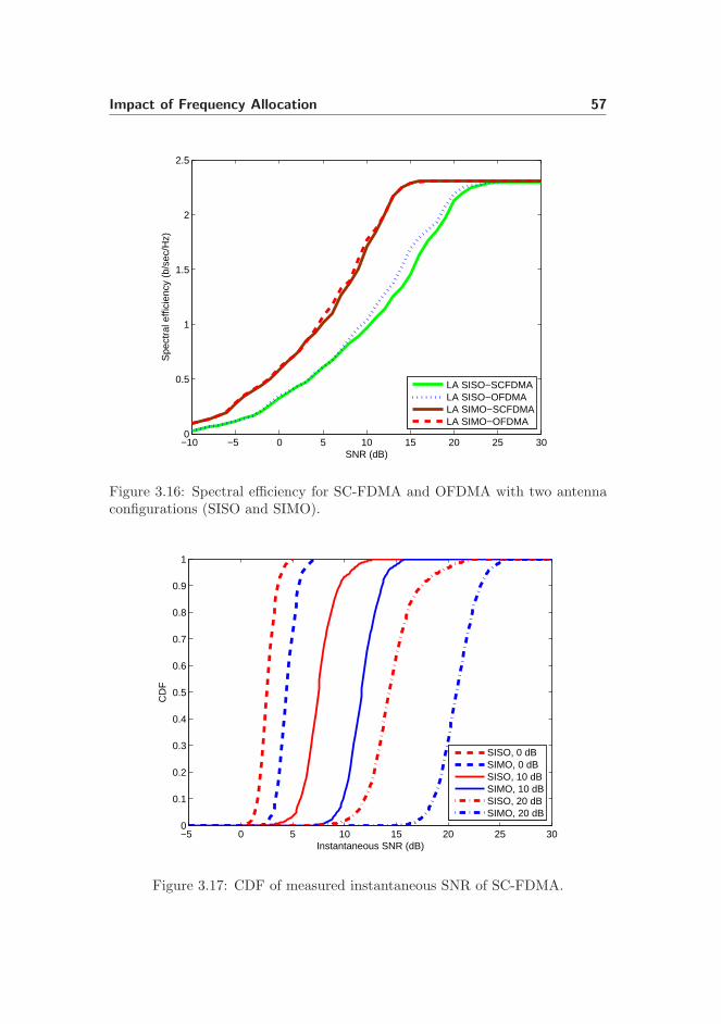
Impact of Frequency Allocation 57
−10 −5 0 5 10 15 20 25 300
0.5
1
1.5
2
2.5
SNR (dB)
Spe
ctra
l effi
cien
cy (
b/se
c/H
z)
LA SISO−SCFDMALA SISO−OFDMALA SIMO−SCFDMALA SIMO−OFDMA
Figure 3.16: Spectral efficiency for SC-FDMA and OFDMA with two antennaconfigurations (SISO and SIMO).
−5 0 5 10 15 20 25 300
0.1
0.2
0.3
0.4
0.5
0.6
0.7
0.8
0.9
1
Instantaneous SNR (dB)
CD
F
SISO, 0 dBSIMO, 0 dBSISO, 10 dBSIMO, 10 dBSISO, 20 dBSIMO, 20 dB
Figure 3.17: CDF of measured instantaneous SNR of SC-FDMA.

58 Baseline LTE Uplink Performance Analysis
Available allocated sub-carriers
Available allocated sub-carriers
1 2 3 4 N
...1 2 3 4 N
Sub-carrier
Index
Sub-carrier
Index
Used sub-carriers
Used sub-carriers...
Localized Transmission
Distributed Transmission
...
Figure 3.18: Localized and distributed frequency allocation in LTE uplink.
SC-FDMA can be used to simplify subcarrier allocation and benefit from op-portunistic scheduling. Lately, the 3GPP only considered the localized case andnot the distributed case since the localized case with frequency hopping can alsogain the frequency diversity. Moreover, the distributed case is sensitive to thefrequency error.
The BLER performance of the distributed and localized case in SC-FDMA withHARQ is presented in Figure 3.19. The SIMO case is assumed, and the channelbandwidth is 10 MHz. A 2.5 MHz bandwidth is allocated for the transmission.For the distributed case, this configuration will allow a repetition factor of 4 sinceall the subcarriers carrying data are spread over the full 10 MHz bandwidth.
It is shown that the distributed cases perform better than the localized one inmost cases. For BLER 1%, it is clear that the distributed case is superior tothe localized. It has around 1 dB gain over localized in 16QAM rate 4/5. Thedistributed case can maximize the frequency diversity by distributing the datain the whole bandwidth. In the real situation, when real channel estimationis taken into account, the localized is expected to perform better than the dis-tributed. The reason is that considering the limited amount of pilot signals, thedistributed has to estimate the channel transfer function in the full bandwidth,whereas the localized estimates the channel transfer function only in the allo-cated channel bandwidth. Thus, the distributed case is more sensitive to theerror introduced by channel estimation.

Impact of Vehicle Speed 59
−10 −8 −6 −4 −2 0 2 4 6 8 10 12 14 16 18
10−2
10−1
100
SNR (dB)
Blo
ck E
rror
Rat
e
QPSK 1/2 DistQPSK 1/2 LocQPSK 3/4 DistQPSK 3/4 Loc16QAM 1/2 Dist16QAM 1/2 Loc16QAM 2/3 Dist16QAM 2/3 Loc16QAM 4/5 Dist16QAM 4/5 Loc
Figure 3.19: BLER performance of Distributed versus Localized in SC-FDMA.
3.11 Impact of Vehicle Speed
The impact of the UE speed on SC-FDMA and OFDMA is discussed. Forthe transmission over time varying and frequency selective fading channel, thereceiver requires to estimate the channel transfer function in both time andfrequency domain. The receiver utilizes the received pilot signals as describedin Section 3.2 to perform channel estimation. In this work, the frequency domainchannel estimation is based on Wiener filter as described in [45]. For the timedomain, a linear interpolation is assumed. The detailed description on thechannel estimation is presented in Appendix A.1.
LTE uplink must be operable at the high speed scenario. Figure 3.20 showsthe results for the speed of 120 km/h. It is shown that OFDMA performance ismore affected by the UE speed than SC-FDMA, especially at higher modulationand coding schemes (16QAM rate 4/5). The UE at high speed has a higherdoppler frequency and creates Inter-Carrier Interference (ICI). In OFDM, eachsubcarrier carries different symbols, and therefore OFDM is more sensitive tothe ICI.
Figure 3.21 illustrates the results for the speed of 200 km/h. It is shown that16QAM rate 3/4 and above does not contribute to the link adaptation curves andoperates at low spectral efficiency. At high speed, the subcarrier orthogonalityis destroyed by the ICI.
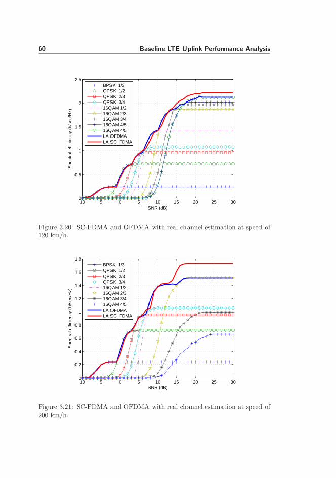
60 Baseline LTE Uplink Performance Analysis
−10 −5 0 5 10 15 20 25 300
0.5
1
1.5
2
2.5
SNR (dB)
Spe
ctra
l effi
cien
cy (
b/se
c/H
z)
BPSK 1/3QPSK 1/2QPSK 2/3QPSK 3/416QAM 1/216QAM 2/316QAM 3/416QAM 4/516QAM 4/5LA OFDMALA SC−FDMA
Figure 3.20: SC-FDMA and OFDMA with real channel estimation at speed of120 km/h.
−10 −5 0 5 10 15 20 25 300
0.2
0.4
0.6
0.8
1
1.2
1.4
1.6
1.8
SNR (dB)
Spe
ctra
l effi
cien
cy (
b/se
c/H
z)
BPSK 1/3QPSK 1/2QPSK 2/3QPSK 3/416QAM 1/216QAM 2/316QAM 3/416QAM 4/5LA OFDMALA SC−FDMA
Figure 3.21: SC-FDMA and OFDMA with real channel estimation at speed of200 km/h.

Turbo Equalization for Performance Improvement 61
3.12 Turbo Equalization for Performance Improve-ment
In this work a turbo equalizer to improve Single Carrier Frequency DivisionMultiple Access (SC-FDMA) performance in the context of LTE uplink is pro-posed. Turbo equalization is an advanced iterative equalization and decodingtechniques that allows enhancement of the performance for the transmissionover a frequency selective fading channel. The turbo equalizer increases the re-ceiver complexity. Nevertheless, the implementation is performed in the node-B,which does not have so stringent physical constraints and power consumptionas the user equipment.
The proposed turbo equalization is based on a new adaptive coefficients solutionfor the frequency domain equalization. The detailed description of the proposedturbo equalizer is presented in Appendix. C.
The simulation results are obtained through Monte Carlo simulations, using a10 MHz system bandwidth in the usage of 600 useful subcarriers. The COST259 Typical Urban with power delay profile 6 paths is assumed [46]. A 1x2SIMO antenna scheme has been considered. All the simulation parameters areshown in Table 3.2.
Figure 3.22 shows the BLER (Block Error Rate) performances of the SC-FDMA16 QAM system with three different coding rates. The results of TEQ withdifferent iterations and SC-FDMA with simple MMSE are given. Two differentresults for turbo equalization are plotted with 2 and 4 iterations of the algorithm,respectively. Compared with the MMSE receiver, the turbo equalizer shows again of around 1 dB. In our assumptions, the cyclic prefix allows completeremoval of the ISI, hence the gain is exclusively due to the reduction of thenoise component. The significant gain is already obtained from 2 iterations ofthe algorithm.
In Figure 3.23 the performance of OFDMA has also been included, and theresults are shown for both QPSK and 16 QAM modulations. The purposeis to compare with the SC-FDMA TEQ receiver performance for 2 iterationsof the algorithm. Note that for QPSK 2/3 and QPSK 3/4 the SC-FDMAwith MMSE system performs better than OFDMA. This is due to the factthat low order modulation schemes are robust to the noise enhancement of SC-FDMA transmission. Moreover, OFDM transmission is more sensitive to thecoding rate than SC-FDMA [12]. SC-FDMA takes advantage of spreading thedata symbols over the transmission bandwidth, where the effect of a deep fadeaffecting few subcarriers will be diminished in the receiver combining all the

62 Baseline LTE Uplink Performance Analysis
0 2 4 6 8 10 12 1410
−2
10−1
100
SNR (dB)
Blo
ck E
rror
Rat
e
MMSETEQ 2xTEQ 4x
16QAM 1/2
16QAM 2/3
16QAM 4/5
Figure 3.22: BLER performance for SC-FDMA 1x2 MRC with and withoutTurbo Equalizer in TU 06 channel.
−4 −2 0 2 4 6 8 10 12 14
10−2
10−1
100
SNR (dB)
Blo
ck E
rror
Rat
e
SC−FDMA MMSEOFDMASC−FDMA TEQ
16QAM 4/5
16QAM 2/3
16QAM 1/2
QPSK 3/4
QPSK 2/3
QPSK 1/2
Figure 3.23: BLER performance for SC-FDMA versus OFDMA in TU 06 chan-nel.

Turbo Equalization for Performance Improvement 63
−10 −8 −6 −4 −2 0 2 4 6 8 10 12 14 16 18 200
0.2
0.4
0.6
0.8
1
1.2
1.4
1.6
1.8
2
2.2
2.4
SNR (dB)
Spe
ctra
l effi
cien
cy (
b/se
c/H
z)
BPSK 1/3QPSK 1/2QPSK 2/3QPSK 3/416QAM 1/216QAM 2/316QAM 3/416QAM 4/5LA MMSELA TEQ
Figure 3.24: Spectral efficiency for SC-FDMA in TU 06 channel.
subcarriers information.
The receiver with turbo equalizer gives better performance in most cases, andin the worst case it shows the same performance as OFDMA. Therefore, turboequalizer makes it possible to reduce the noise enhancement due to the timedomain transmission in the SC-FDMA system, and makes performance the sameor better than OFDMA. The gain depends mostly on the usage of equalizationwith adaptive coefficients.
The performance results for several modulation and coding schemes in terms ofspectral efficiency are shown in Figure 3.24. The figure shows the link adapta-tion curve for both the MMSE and the TEQ receiver. It is shown that the turboequalization is effective for higher order MCS, whereas for BPSK it does notshow any performance improvement. Therefore, in order to exploit its perfor-mance gain, the turbo equalizer receiver could be used for high order modulationschemes, whereas the simple MMSE receiver can still be used for BPSK. In thisway, the computational load for low order modulations can be reduced.
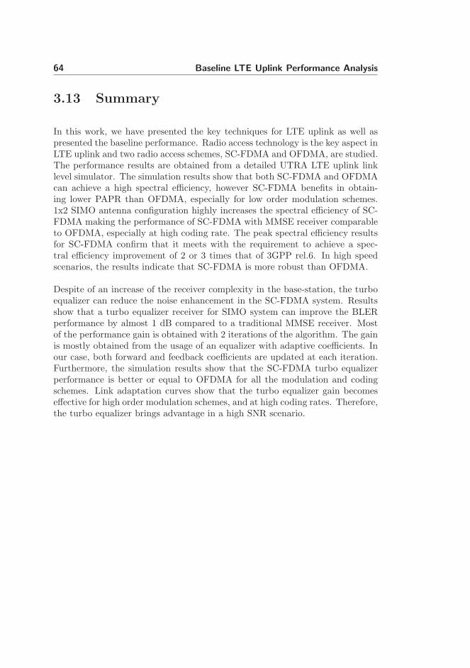
64 Baseline LTE Uplink Performance Analysis
3.13 Summary
In this work, we have presented the key techniques for LTE uplink as well aspresented the baseline performance. Radio access technology is the key aspect inLTE uplink and two radio access schemes, SC-FDMA and OFDMA, are studied.The performance results are obtained from a detailed UTRA LTE uplink linklevel simulator. The simulation results show that both SC-FDMA and OFDMAcan achieve a high spectral efficiency, however SC-FDMA benefits in obtain-ing lower PAPR than OFDMA, especially for low order modulation schemes.1x2 SIMO antenna configuration highly increases the spectral efficiency of SC-FDMA making the performance of SC-FDMA with MMSE receiver comparableto OFDMA, especially at high coding rate. The peak spectral efficiency resultsfor SC-FDMA confirm that it meets with the requirement to achieve a spec-tral efficiency improvement of 2 or 3 times that of 3GPP rel.6. In high speedscenarios, the results indicate that SC-FDMA is more robust than OFDMA.
Despite of an increase of the receiver complexity in the base-station, the turboequalizer can reduce the noise enhancement in the SC-FDMA system. Resultsshow that a turbo equalizer receiver for SIMO system can improve the BLERperformance by almost 1 dB compared to a traditional MMSE receiver. Mostof the performance gain is obtained with 2 iterations of the algorithm. The gainis mostly obtained from the usage of an equalizer with adaptive coefficients. Inour case, both forward and feedback coefficients are updated at each iteration.Furthermore, the simulation results show that the SC-FDMA turbo equalizerperformance is better or equal to OFDMA for all the modulation and codingschemes. Link adaptation curves show that the turbo equalizer gain becomeseffective for high order modulation schemes, and at high coding rates. Therefore,the turbo equalizer brings advantage in a high SNR scenario.

“ The greatest barrier to success is thefear of failure.”
Sven Goran Eriksson
Chapter 4
RF Hardware ImperfectionsEffect on Inband Channel
4.1 Introduction
The performance of a radio link is also affected by the quality of the RF trans-mitter architecture. Each RF transmitter architecture has the advantage anddisadvantage, including different RF imperfections, as explained in Chapter 2.The imperfections in each RF architecture can be modeled for further investiga-tion in a link level or system level study. A consistent RF imperfections modelis required for the 3GPP work item phase which cannot be based on a specificRF architecture. Nevertheless, it is also difficult to make the study completelyindependent from the RF architecture because some imperfections are specificto some architectures. For example, the gain and phase imbalance are producedin the Cartesian transmitter architecture and the envelope and phase timingalignment problem are in the Polar transmitter architecture.
Here, the validity of a simplified RF imperfection model is investigated in orderto understand what scope of applicability it may have in a practical context,especially for the LTE 3GPP work. The investigation is focused on the impactof the imperfections on the in-band channel. The impact on the out-of bandchannel is also important and addressed in Chapter 5. The aim of this work isto link the individual RF imperfections Error Vector Magnitude (EVM) char-

66 RF Hardware Imperfections Effect on Inband Channel
acteristics to the link level performance, especially to obtain clear insight in thesensitivity on each RF imperfection. The link level performance is evaluated forAWGN and frequency selective fading channels. Performance evaluation in anAWGN channel represents the conditions under which EVM measurements areobtained for type approval, whereas the performance evaluation in frequency se-lective fading is more representative of actual operating conditions. The relationbetween different RF transmitter imperfection models in LTE uplink and howaccurately the effect of each RF imperfection can be modelled by an equivalentwhite Gaussian noise source in the transmitter are also investigated.
The impact of each imperfection in a Cartesian transmitter on LTE uplink linkperformance is investigated. The most common imperfections, such as nonlinearpower amplifier, gain imbalance, phase imbalance, DC offset, and phase noise areconsidered. The imperfection model is taken from an established imperfectionmodel. Each imperfection is characterized by means of error vector magnitude(EVM) and equivalent link performance loss [47],[48],[14]. To simplify the mod-elling of RF imperfections on link and system performance, a simple AWGNgenerator in the transmitter is often used with a variance set according to aspecific EVM level; e.g. as reported in [47] for the High Speed Downlink PacketAccess (HSDPA) system. In this study, the applicability of the simple AWGNgenerator in the transmitter on beyond 3G system is carried out. For the casestudy, LTE uplink is considered.
This chapter is organized as follows. First, the EVM measurement definitionin the LTE uplink is given in Section 4.2. Section 4.3 describes the used sim-ulation models for the considered RF transmitter imperfections. Performanceevaluation of EVM and the impact on link level performance are discussed inSection 4.4. Finally, the summary is given in Section 4.5.
4.2 LTE EVM Measurement
EVM is commonly used as a direct measure of the transmitter signal quality,in particular when related to any RF hardware imperfections in the system.EVM does not cover the aspect of disturbance to other users where AdjacentChannel Leakage Ratio (ACLR) must be used [15]. The EVM is a measureof the difference between the measured and the reference signals. In LTE, theEVM is measured in the constellation domain [49, 50, 51] rather than in timedomain as for the previous UTRA specifications [52]. This approach allows pre-/post FFT time/frequency synchronization and amplitude/phase correction tobe included in the frequency domain equalization block at the receiver as shownin Figure 4.1. Therefore, the filter group delay and amplitude/phase errors can
RF Imperfections Model 67
be compensated before the EVM calculation. The implication is that the filterdoes not have to be specified in the standard as it was previously specified FORUTRA WCDMA system.
The EVM is measured at the symbol detection input as shown in Fig. 4.1, andcan be calculated as [49]:
EV Mm =
√√√√∑L
l=0
∑K−1k=0 |Zl(k) − Rl(k)|2
∑Ll=0
∑K−1k=0 |Rl(k)|2
∗ 100% (4.1)
Where Zl(k) and Rl(k) are the k-th complex baseband constellation point of thel-th measured SC-FDMA symbol and reference SC-FDMA symbols, respectively.L is the number of SC-FDMA symbols in one sub-frame, and K is the size ofthe resource block in one SC-FDMA symbol.
In our work, the final EVM measurement is achieved as an average over time[49]:
EV M =1
M
M∑
m=1
EV Mm (4.2)
where M is the number of sub-frames, used for averaging.
4.3 RF Imperfections Model
The RF imperfection is located in the transmitter as depicted in Figure 4.1.In this section, a modelling of the most common RF transmitter imperfectionsused is described, including nonlinear power amplifier, phase noise, gain andphase imbalances, DC offset, and the equivalent white noise source.
4.3.1 Nonlinear Power Amplifier
The nonlinear power amplifier is usually characterized by AM/AM and AM/PMdistortion curves. This nonlinearity phenomena lead to performance degrada-tion and spectral regrowth. The AM/AM and AM/PM characteristics used inthis study represented as |S21| and ∠S21, are shown in Figure 4.2. These charac-teristics are based on the measurement result of a UE wideband CDMA poweramplifier (PA) module [4]. This PA has a good compromise between linearityand power efficiency for varying envelope input signal. From Figure 4.2, the

68 RF Hardware Imperfections Effect on Inband Channel
DFT IFFT
FFTEqualizerIDFT
Symbol
Detection/
Decoding
EVM
Measurement
Point
Pre/Post FFT
Time / Frequency
Sycnhronization
Tx Modulation Processing
Rx Demodulation Processing
RF
Imper-
fections
S/PConstellation
MappingAdd
CPP/S
Remove
CPS/PP/S
Figure 4.1: SC-FDMA modulation/demodulation and EVM measurement point.
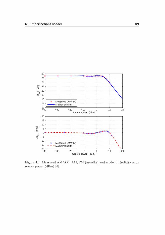
RF Imperfections Model 69
−40 −30 −20 −10 0 10 2012
14
16
18
20
22
24
26
28
Source power [dBm]
|S21
| [d
B]
−40 −30 −20 −10 0 10 20−20
−15
−10
−5
0
5
10
15
20
Source power [dBm]
∠S
21
[deg
]
Measured (AM/PM)Mathematical fit
Measured (AM/AM)Mathematical fit
Figure 4.2: Measured AM/AM, AM/PM (asteriks) and model fit (solid) versussource power (dBm) [4].
70 RF Hardware Imperfections Effect on Inband Channel
power amplifier has 27 dB linear gain and 1 dB compression point at +6.1 dBminput power.
The results shown in Figure 4.2 is the S21 parameter or the voltage gain as afunction of the input power level Pi. S21 can be expressed as [53]:
S21 → S21 (Pi) = α (Pi) · exp [jθ (Pi)] (4.3)
Where Pi is the time-varying input envelope power. The general expression ofthe input signal is given by:
x (t) = a (t) · cos (2πf0t + φ (t)) (4.4)
Where a (t),φ (t),f0 are the envelope of the input signal, the time varying phaseof the input signal, and the carrier frequency, respectively. Applying the non-linear model, the output signal can be expressed as follows:
y (t) = fa (a (t) · cos (2πf0t + fφ (a (t) , φ (t)))) (4.5)
Where fa and fΦ are nonlinear distortion functions of input power and phasegiven by:
fa (a (t)) = a (t) · α (Pi (T )) (4.6)
fΦ (a (t) ,Φ(t)) = Φ (t) + Φ (Pi (T )) (4.7)
The instantaneous input power Pi(t) can be expressed as:
Pi (t) =a2 (t)
2Z0(4.8)
In most practical cases, the load impedance Z0 is equal to the input and outputimpedance with a value of 50 ohm.
For the nonlinear modelling purpose, it is necessary to know the α and θ func-tions. Following the approach in [53], a power series function can be used tomodel the |S21| and ∠S21 which represent the AM/AM and AM/PM distortionfunctions.
α (Pi (t)) =
M∑
m=0
αm · Pmi (t) (4.9)
Φ (Pi (t)) =M∑
m=0
Φm · Pmi (t) (4.10)
In (4.9) and (4.9), M is the order of the power series model. Applying thisapproach, the power amplifier measurement can be approximated as shown in

RF Imperfections Model 71
Figure 4.2. The results show that an 8th order power series fit well with themeasurement results when suitable extrapolation is made towards lower andhigher source power, respectively.
The power amplifier efficiency is shown in [53]. For this type of power amplifier,an efficiency of 38% is achieved at the output power of 30 dBm.
4.3.2 Gain & Phase Imbalances
The impact of gain and phase imbalances on the transmitted output signal isdescribed in Section 2.3. The mathematical modelling is given in (2.9)-(2.11),with the gain imbalance α and phase imbalance θ:
α = 10(α/20) , α in dB (4.11)
θ = (θ/180) π , θ in degree (4.12)
4.3.3 Phase Noise
Phase noise causes inter-carrier interference (ICI) and common phase error(CPE) [13]. The common phase error creates a fixed phase rotation in eachSC-FDMA symbol and as discussed previously, it is assumed that the receiverfully compensates the CPE to minimize EVM and link performance degrada-tion. The phase noise is modeled by a Wiener-Levy process as described inSection 2.3. In a discrete time model, the phase noise can be modeled as aMarkov process. The random phase value of the affected subcarrier at the nth
sample of the mth SC-FDMA symbol can be written as:
Φm [n] = Φm−1 [Ngs − 1] +
n∑
i=0
u [mNgs + i] (4.13)
where u [i] is a white Gaussian random process with zero mean and varianceσu = 2π∆f3dB
TNs
, and T denotes the SC-FDMA symbol period. Ns is the FFTsize.
The power spectral density of (4.13) is the phase noise SSB as the function ofthe 3dB phase noise bandwidth ∆f3dB parameter and is shown in Fig. 4.3. Thephase noise power spectral density is following the Lorentzian spectrum with a
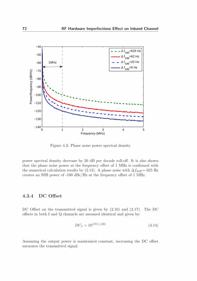
72 RF Hardware Imperfections Effect on Inband Channel
0 1 2 3 4 5−140
−130
−120
−110
−100
−90
−80
−70
−60
−50
−40
Frequency (MHz)
Pow
er/fr
eque
ncy
(dB
/Hz)
∆ f
3dB=625 Hz
∆ f3dB
=62 Hz
∆ f3dB
=20 Hz
∆ f3dB
=6 Hz
1MHz
Figure 4.3: Phase noise power spectral density
power spectral density decrease by 20 dB per decade roll-off. It is also shownthat the phase noise power at the frequency offset of 1 MHz is confirmed withthe numerical calculation results by (2.13). A phase noise with ∆f3dB= 625 Hzcreates an SSB power of -100 dBc/Hz at the frequency offset of 1 MHz.
4.3.4 DC Offset
DC Offset on the transmitted signal is given by (2.16) and (2.17). The DCoffsets in both I and Q channels are assumed identical and given by:
DCI = 10(DCI/20) (4.14)
Assuming the output power is maintained constant, increasing the DC offsetsaturates the transmitted signal.
Evaluation of Inband Performance 73
4.3.5 White Noise Source
An approach to simplify the RF imperfection modelling effort is proposed. Themodel is based on a white noise source in the RF transmitter. This model hasthe restriction that can only be used to investigate the link level performancedegradation due to the RF transmitter imperfection. The effect on the out-ofband spectrum cannot be investigated based on this model.
The white noise source introduces the noise in the transmitted signal. Thetransmitted output signal affected by the white noise source imperfection iswritten as:
y (t) = a (t) + 10σ2
S
σ2
M
/20(4.15)
The noise variance of this white noise source model σ2M at the transmitter is
set by a desired ratio compared to the variance of the transmitted signal σ2S .
Hence, the signal to noise ratio at the transmitter is given by:
S
M=
σ2S
σ2M
(4.16)
The transmitter noise generates EVM and the relation between the EVM andsignal to noise ratio at the transmitter is given by:
S
M= −20 log(EV M) (4.17)
4.4 Evaluation of Inband Performance
The performance evaluation of LTE uplink performance with the presence ofhardware imperfections is carried out in a computer-based Monte Carlo simu-lation. The simulation is performed in accordance with the LTE uplink mainparameters given in Table 4.1 unless otherwise specified. The details on thelink level processing can be found in Appendix. A. During the simulation, thefollowing assumptions are made:
• Both transmitter and receiver are perfectly synchronized in time and fre-quency.
• The maximum excess delay of the frequency selective fading channel isshorter than the cyclic prefix duration.

74 RF Hardware Imperfections Effect on Inband Channel
Table 4.1: UTRA LTE uplink simulation parameters.
Parameter Value
Carrier Frequency 2 GHz
Transmission BW 10 MHz
Sub-frame duration 0.5 ms
Sub-carrier spacing 15 kHz
SC-FDM symbols/TTI 6 LBs, 2 SBs
CP duration 4.1 µs
FFT size/Useful subcarriers 1024/600
MCS settings QPSK: 1/2 , 2/3, 3/4,
16QAM: 1/2 , 2/3, 3/4
Channel code 3GPP Rel. 6 compliant Turbo code
with basic rate 1/3
Receiver MMSE Receiver
Channel Estimation Ideal
Antenna schemes SISO
Channel model AWGN, Typical Urban 6 paths [5]
Speed 3 kmph
HARQ No
RF imperfections Nonlinear PA, Phase Noise,
Gain and Phase Imbalances, DC offset
White noise source
• The receiver performs ideal channel estimation. So that, it will not intro-duce additional performance degradation.
• One sub-frame consists of 6 Long Blocks (LBs) for data and 2 Short Blocks(SBs) for reference signals (14% overhead).
The power amplifier has an important role in the LTE uplink due to the high sig-nal envelope variation, and resulting distortion which can affect the LTE perfor-mance. Figure 4.4 shows the EVM results for both SC-FDMA and OFDMA airinterfaces. The results for both modulations, QPSK and 16QAM are presented.SC-FDMA has better EVM performance compared to OFDMA. A Change tolower modulation, QPSK, further improve the SC-FDMA performance, whilethis is not the case for OFDMA. These results are due to the fact that SC-FDMA has lower PAPR than OFDMA as shown in Figure 3.5 and Figure 3.6.OFDMA which has higher PAPR suffers from the nonlinear power amplifier.

Evaluation of Inband Performance 75
−6 −4 −2 0 2 4 6 8 10 12 14 160
4
8
12
16
20
24
Pin
(dBm)
EV
Mrm
s (%
)
16QAM OFDMQPSK OFDM16QAM SCFDMAQPSK SC−FDMA
1dB compression point
Figure 4.4: EVM results for Nonlinear PA
Figure 4.5 shows the EVM results for SC-FDMA with various number of sub-carriers. The number of sub-carriers is represented by the number of resourceblocks (RB)s in which one resoure block consists of 12 sub-carriers. Theseresults show that the number of sub-carriers/RBs does not affect much on theEVM results. The EVM variation is within 1%. This result is also in goodagreement with the result shown in Figure 3.8 in which increasing the numberof sub-carriers doe not affect the PAPR.
The impact of the non-linear power amplifier to the SC-FDMA and OFDMAspectral efficiency is shown in Figure 4.6. These results are obtained when aninput back off (IBO) of 4 dB is assumed to maintain high efficiency. The resultin the ideal case when there is no nonlinear PA is also given and represented inthe link adaptation curve. It is shown that the nonlinear PA slightly reduce theSC-FDMA performance at higher modulation and coding scheme. In general,the nonlinear PA is also mainly affecting the higher order modulation and cod-ing scheme for both SC-FDMA and OFDMA. A performance loss of 1.2 dB isobserved for OFDMA with 16QAM 4/5.
Figure 4.7 summarizes the performance loss due the nonlinear PA at a BLERtarget of 10%. For 16QAM rate 4/5, SC-FDMA has a gain of 0.7 dB overOFDMA. A small gain of 0.2 dB can still be obtained at the lower coding rate.These results confirm that SC-FDMA radio access technique is the preferredsolution over OFDMA in the presence of nonlinear power amplifier.
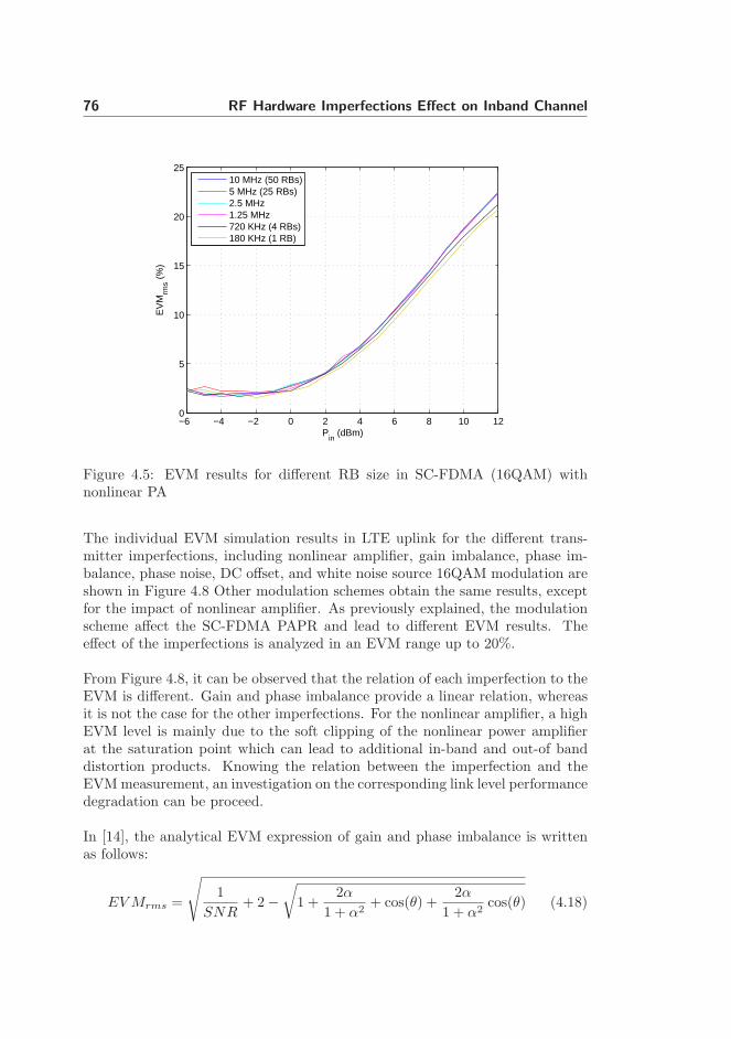
76 RF Hardware Imperfections Effect on Inband Channel
−6 −4 −2 0 2 4 6 8 10 120
5
10
15
20
25
Pin
(dBm)
EV
Mrm
s (%
)
10 MHz (50 RBs)5 MHz (25 RBs)2.5 MHz1.25 MHz720 KHz (4 RBs)180 KHz (1 RB)
Figure 4.5: EVM results for different RB size in SC-FDMA (16QAM) withnonlinear PA
The individual EVM simulation results in LTE uplink for the different trans-mitter imperfections, including nonlinear amplifier, gain imbalance, phase im-balance, phase noise, DC offset, and white noise source 16QAM modulation areshown in Figure 4.8 Other modulation schemes obtain the same results, exceptfor the impact of nonlinear amplifier. As previously explained, the modulationscheme affect the SC-FDMA PAPR and lead to different EVM results. Theeffect of the imperfections is analyzed in an EVM range up to 20%.
From Figure 4.8, it can be observed that the relation of each imperfection to theEVM is different. Gain and phase imbalance provide a linear relation, whereasit is not the case for the other imperfections. For the nonlinear amplifier, a highEVM level is mainly due to the soft clipping of the nonlinear power amplifierat the saturation point which can lead to additional in-band and out-of banddistortion products. Knowing the relation between the imperfection and theEVM measurement, an investigation on the corresponding link level performancedegradation can be proceed.
In [14], the analytical EVM expression of gain and phase imbalance is writtenas follows:
EV Mrms =
√1
SNR+ 2 −
√1 +
2α
1 + α2+ cos(θ) +
2α
1 + α2cos(θ) (4.18)

Evaluation of Inband Performance 77
−10 −5 0 5 10 15 20 250
0.5
1
1.5
2
2.5
SNR (dB)
Spe
ctra
l effi
cien
cy (
b/se
c/H
z)
−10 −5 0 5 10 15 20 250
0.5
1
1.5
2
2.5
SNR (dB)
Spe
ctra
l effi
cien
cy (
b/se
c/H
z)
π/2 BPSK 1/3QPSK 1/2QPSK 2/3QPSK 3/416QAM 1/216QAM 2/316QAM 3/416QAM 4/5LA (NLA)LA (no imperfect)
π/2 BPSK 1/3QPSK 1/2QPSK 2/3QPSK 3/416QAM 1/216QAM 2/316QAM 3/416QAM 4/5LA (NLA)LA (no imperfect)
SC−FDMA
OFDMA
Figure 4.6: Spectral efficiency degradation for various MCS in the presence ofnonlinear PA
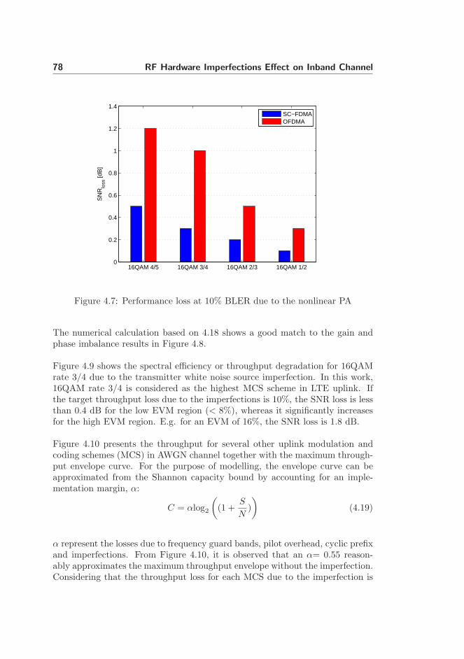
78 RF Hardware Imperfections Effect on Inband Channel
16QAM 4/5 16QAM 3/4 16QAM 2/3 16QAM 1/20
0.2
0.4
0.6
0.8
1
1.2
1.4S
NR
loss
[dB
]
SC−FDMAOFDMA
Figure 4.7: Performance loss at 10% BLER due to the nonlinear PA
The numerical calculation based on 4.18 shows a good match to the gain andphase imbalance results in Figure 4.8.
Figure 4.9 shows the spectral efficiency or throughput degradation for 16QAMrate 3/4 due to the transmitter white noise source imperfection. In this work,16QAM rate 3/4 is considered as the highest MCS scheme in LTE uplink. Ifthe target throughput loss due to the imperfections is 10%, the SNR loss is lessthan 0.4 dB for the low EVM region (< 8%), whereas it significantly increasesfor the high EVM region. E.g. for an EVM of 16%, the SNR loss is 1.8 dB.
Figure 4.10 presents the throughput for several other uplink modulation andcoding schemes (MCS) in AWGN channel together with the maximum through-put envelope curve. For the purpose of modelling, the envelope curve can beapproximated from the Shannon capacity bound by accounting for an imple-mentation margin, α:
C = αlog2
((1 +
S
N)
)(4.19)
α represent the losses due to frequency guard bands, pilot overhead, cyclic prefixand imperfections. From Figure 4.10, it is observed that an α= 0.55 reason-ably approximates the maximum throughput envelope without the imperfection.Considering that the throughput loss for each MCS due to the imperfection is

Evaluation of Inband Performance 79
22 24 26 28 30 32 340
5
10
15
20
Output Power (dBm)
EV
Mrm
s (%
)
0 1 2 3 40
5
10
15
20
Gain imbalance (dB)
EV
Mrm
s (%
)
0 4 8 12 160
5
10
15
20
Phase imbalance (degree)
EV
Mrm
s (%
)−120 −115 −110 −105 −100
0
5
10
15
20
SSB Power at 1 MHz (dBc/Hz)
EV
Mrm
s (%
)
121518212427300
5
10
15
20
Signal to White noise ratio (dB)
EV
Mrm
s (%
)
−36 −32 −28 −24 −20 −160
5
10
15
20
DC Offset (dB)
EV
Mrm
s (%
)
PA Compression
Gain Imbalance
Phase Noise
White Noise Source
Phase Imbalance
DC Offset
Figure 4.8: EVM results for various RF Imperfections
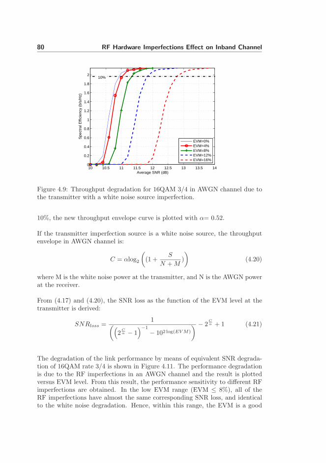
80 RF Hardware Imperfections Effect on Inband Channel
10 10.5 11 11.5 12 12.5 13 13.5 140
0.2
0.4
0.6
0.8
1
1.2
1.4
1.6
1.8
2
Average SNR (dB)
Spe
ctra
l Effi
cien
cy (
b/s/
Hz)
EVM=0%EVM=4%EVM=8%EVM=12%EVM=16%
10%
Figure 4.9: Throughput degradation for 16QAM 3/4 in AWGN channel due tothe transmitter with a white noise source imperfection.
10%, the new throughput envelope curve is plotted with α= 0.52.
If the transmitter imperfection source is a white noise source, the throughputenvelope in AWGN channel is:
C = αlog2
((1 +
S
N + M)
)(4.20)
where M is the white noise power at the transmitter, and N is the AWGN powerat the receiver.
From (4.17) and (4.20), the SNR loss as the function of the EVM level at thetransmitter is derived:
SNRloss =1((
2Cα − 1
)−1
− 102 log(EV M)
) − 2Cα + 1 (4.21)
The degradation of the link performance by means of equivalent SNR degrada-tion of 16QAM rate 3/4 is shown in Figure 4.11. The performance degradationis due to the RF imperfections in an AWGN channel and the result is plottedversus EVM level. From this result, the performance sensitivity to different RFimperfections are obtained. In the low EVM range (EVM ≤ 8%), all of theRF imperfections have almost the same corresponding SNR loss, and identicalto the white noise degradation. Hence, within this range, the EVM is a good

Evaluation of Inband Performance 81
0 2 4 6 8 10 12 14
0.5
1
1.5
2
2.5
3
SNR (dB)
Spe
ctra
l Effi
cien
cy (
b/se
c/H
z)
QPSK 1/2QPSK 2/3QPSK 3/416QAM 1/216QAM 2/316QAM 3/416QAM 4/5Shannon (α=0.55)Shannon (α=0.52)
Figure 4.10: Approximating the maximum capacity of MCS envelope in AWGNChannel.
direct measure to estimate the link level performance loss. At high EVM levels,the SNR loss for each imperfection starts to deviate from the equivalent whitenoise source imperfection.
In Figure 4.11, phase noise has higher SNR loss compared to other imperfections.This was expected because the phase noise introduces inter-carrier interferencewhich is more severe than additive noise. Nevertheless, practical oscillators onlyleads to low phase noise level, and small EVM. For example, in GSM/WCDMAapplications a typical phase noise level is around -120 dBc/Hz at 1 MHz offset[54] which keeps the corresponding EVM below 2%. At the opposite end, gainimbalance introduces less performance degradation. The performance loss dueto the nonlinear power amplifier is slightly higher than the loss due to the whitenoise source.
The result from (4.21) is also plotted in Figure 4.11. It can be observed thatthe derived calculation of the SNR loss due to the white noise source at thetransmitter matches the simulation results. There is only a small deviation of0.1 dB at high EVM levels (EVM=20%).
The result for higher MCS with 16QAM rate 4/5 is shown in Figure 4.12. Itis shown that the higher MCS is more sensitive to the EVM. The result showsthat most of the imperfections again have similar SNR loss results in the lowEVM region (EVM ≤ 7%). The result of analytical model with the white noise

82 RF Hardware Imperfections Effect on Inband Channel
2 4 6 8 10 12 14 16 18 200
0.5
1
1.5
2
2.5
3
3.5
4
4.5
5
EVMrms
(%)
SN
Rlo
ss (
dB)
Phase NoiseNonlinear PAWhite Noise SourcePhase ImbalanceDC OffsetGain ImbalanceWhite Noise (Analytical)
Figure 4.11: SNR loss for 16QAM 3/4 due to the RF imperfections (AWGN).
source is still in good agreement with the simulation result.
Figure 4.13 shows the relation between EVM value and equivalent SNR degra-dation in TU06 channel. The results follow the trend in the previous result inthe AWGN channel with an SNR loss range of 5 dB. An analytical result for theeffect of the equivalent white noise source in the TU06 channel is more complexthan in the AWGN channel since the transmitter imperfections can appear asadditional coloured noise at the receiver. Nevertheless, the white noise sourceimperfection model still fits well with the other imperfections, especially in theEVM < 6% region.
Figure 4.14 shows the results the impact of various imperfections to the higherMCS (16QAM rate 4/5) in TU06 channel. Higher MCS is more sensitive towardEVM values, especially at the high EVM range. However, different imperfec-tions, including the white noise source still obtain the same SNR loss in the lowEVM region. Hence, for EVM values less than 6-8%, the white noise source isuseful as an equivalent transmitter imperfection source. Note that the aboveanalysis assumes 16QAM as the maximum modulation order. The final EVMrequirement will be chosen as a compromise among UE complexity and systemperformance. As an arbitrarily chosen reference, an EVM of 8% correspondsto a link loss of 0.5 dB for 16QAM. Recently, in e.g. [55], 64QAM has beenconsidered for uplink which leads to increased effect of EVM.

Evaluation of Inband Performance 83
2 4 6 8 10 12 14 16 18 200
0.5
1
1.5
2
2.5
3
3.5
4
4.5
5
EVMrms
(%)
SN
Rlo
ss (
dB)
Phase NoiseNonlinear AmpWhite NoisePhase ImbalanceDC OffsetGain ImbalanceWhite Noise (Analytical)
Figure 4.12: SNR loss for 16QAM 4/5 due to the RF imperfections (AWGN).
2 4 6 8 10 12 14 16 18 200
0.5
1
1.5
2
2.5
3
3.5
4
4.5
5
EVMrms
(%)
SN
R lo
ss (
dB)
Phase NoiseNonlinear PAWhite Noise SourcePhase ImbalanceDC OffsetGain Imbalance
Figure 4.13: SNR loss for 16QAM 3/4 due to the RF imperfections (TU06).

84 RF Hardware Imperfections Effect on Inband Channel
2 4 6 8 10 12 14 16 18 200
0.5
1
1.5
2
2.5
3
3.5
4
4.5
5
EVMrms
(%)
SN
Rlo
ss (
dB)
Phase NoiseNonlinear AmpWhite NoisePhase ImbalanceDC OffsetGain Imbalance
Figure 4.14: SNR loss for 16QAM 4/5 due to the RF imperfections (TU06).
4.5 Summary
The impact of the RF transmitter imperfections in LTE uplink performance ispresented in this chapter. The results obtained are based on the UTRA LTEuplink parameter settings. The study is focused on the impact on the in-bandchannel performance, especially on EVM and link level performance loss. Fromthis study, the EVM generated by each imperfection can be associated with thecorresponding link level performance.
The most common RF imperfections in the Cartesian transmitter, includingnonlinear power amplifier, gain imbalance, phase imbalance, DC offset, andphase noise are investigated. A white noise source as an equivalent RF transmit-ter imperfection is also investigated. SC-FDMA shows its benefit over OFDMAwhen a nonlinear power amplifier is taking into account. SC-FDMA with16QAM rate 4/5 provides additional gain of 0.7 dB over OFDMA and henceleads to a better spectral efficiency. This result in favour with the selection ofSC-FDMA for the access scheme in LTE.
The EVM is a good direct measure to estimate the link level performance lossin the practical EVM range (EVM < 8%) for the investigated imperfections. Inour simulations, an EVM value of 8% corresponds to an SNR loss of 0.5 dB with

Summary 85
16QAM rate 3/4. The EVM also becomes an important parameter for higherorder modulation and coding scheme, which very sensitive to the imperfections.
The main benefit from this work is to simplify the simulation effort in the studyof RF imperfections, especially by including a white noise source as an equiva-lent model of the RF transmitter imperfections. The performance degradationin AWGN and frequency selective fading when using a white noise source as anequivalent transmitter RF imperfection model, fits well with the other imper-fections in the anticipated range of EVM. With calibrated noise power settingsthis simple noise source may replace individual imperfection models in link levelsimulations.
The RF imperfections not just affect the inband performance. These imperfec-tions can also affect the out-of-band performance lead to interfere the adjacentchannel, and thus a topic for the following chapter, which cover the impact ofRF imperfections on the out-of band channel.

86 RF Hardware Imperfections Effect on Inband Channel

“ Does man think that he will be left uncon-trolled, (without purpose)?”
The Resurrection 75:36
Chapter 5
RF Hardware ImperfectionsEffect on Out-of-band
Channel
5.1 Introduction
RF hardware imperfections are affecting both the in-band and out-of-band chan-nel. The impact on the out-of-band channel is an increase of out-of-band emis-sions. Out-of-band emissions are unwanted emissions immediately outside thenominal channel resulting from the modulation process and non-linearity in thetransmitter, but excluding spurious emissions [6]. The performance of a radiocommunication system in the out-of-band channel is measured by the parame-ters defined by the standard and must meet with the requirements .
SC-FDMA is the new radio access technique in beyond 3G system and offersflexibility for the user to be scheduled in both frequency and time domain toexploit the radio channel variations [8]. In LTE, the user equipment (UE) hasa flexibility to transmit on 1 resource block (RB = 180 kHz) up to 100 RBdepending on the bandwidth allocation from the base station leading to largedynamics in the power spectral density transmitted from the UE. Such dynamicsneed to be considered when analyzing LTE Radio Frequency (RF) requirements.

88 RF Hardware Imperfections Effect on Out-of-band Channel
Each LTE channel bandwidth has its own RF requirements [56].
The spectrum emission of LTE UE must be controlled by a spectrum shapingtechnique in order to meet the stringent spectral mask requirements [57], [58].The flexible UE transmission bandwidth and small guard-band size are themain issues in the area of transmit spectrum shaping for LTE. Currently, itis an open and hot topic in the 3GPP bodies [57],[59],[60],[61]. Moreover, the3GPP has not completely addressed the effectiveness of different techniques inmeeting out of band emission requirements [62]. It is not clear either the 3GPPintends to standardize the spectrum shaping techniques or leave it open to themanufactures [62].
A spectrum shaping technique implemented in the transmitter can provide asufficient margin to the emission mask requirements towards the spectral re-growth as a result of the RF imperfections. Each RF imperfection can createdifferent impact on the transmit signal. Combined with the flexible transmissionbandwidth factor in LTE, it becomes an important issue which is addressed inthis chapter. The placement of the Resource Block in the channel bandwidth isexpected to create different results in terms of the out of band spectrum.
This chapter is organized as follows. The overview of LTE requirements relatedto the out-of band channel is given in Section 5.2. Two different spectrumshaping techniques are described in Section 5.3. Assumptions and scenarios forthe assessment of the spectrum shaping techniques are given in Section 5.4. Forthe spectrum shaping performance results are discussed in Section 5.5. Theimpact of RF hardware imperfections is analyzed in Section 5.6. This sectiondiscusses the impact on different radio access techniques in LTE, and the impacton resource block allocation. Finally, a summary is presented in Section 5.7.
5.2 Out-of-band Channel Requirements
This section provides the out-of-band channel requirements of LTE, which areused as the reference for the subsequent sections. Multiple options of LTE chan-nel bandwidth results in a complex requirement. Each channel bandwidth hasa specific requirement on both Spectrum Emission Mask (SEM) and AdjacentChannel Leakage Ratio (ACLR) requirements1 [56]. The out-of-band channelrequirements are specified in terms of a SEM and ACLR [56]. ACLR and SEMserve different purposes. ACLR captures the average of signal characteristicsover a carrier, while the SEM captures the variation in the spectrum emissions.
1During the work of this thesis, the requirements have not been fully standardized yet.

Out-of-band Channel Requirements 89
Table 5.1: UTRA Spectrum Emission Mask Requirement (SEM) [6].
∆f in freq. Minimum Requirement Meas. BW
(MHz) Relative req. Absolute req.
2.5-3.5{−35 − 15 ·
(∆f
MHz − 2.5)}
dBc -71.1 dBm 30 kHz
3.5-7.5{−35 − 1 ·
(∆f
MHz − 3.5)}
dBc -55.8 dBm 1 MHz
7.5-8.5{−39 − 10 ·
(∆f
MHz − 7.5)}
dBc -55.8 dBm 1 MHz
8.5-12.5 -49 dBc -55.8 dBm 1 MHz
5.2.1 LTE Spectrum Emission Mask (SEM)
In this work the baseline spectrum emission mask is the spectrum emission maskfor UTRA WCDMA, which has a fixed channel bandwidth of 5 MHz [6]. Todefined the spectrum emission mask for other channel bandwidths, the scaledversion of that UTRA WCDMA spectrum emission mask is assumed. TheUTRA WCDMA spectrum emission mask for the UE applies to frequenciesbetween 2.5 MHz and 12.5 MHz away from the UE center carrier frequency asdescribed in Table 5.1.
5.2.2 LTE Adjacent Channel Leakage Ratio (ACLR)
The adjacent channel leakage ratio is defined as a ratio of the power integratedover an assigned bandwidth in the adjacent channel to the power integrated overthe desired channel. Figure 5.1 illustrates the transmit spectrum for the ACLRcalculation. The ACLR can be expressed as:
ACLR =
∫ f1+∆BACP
f1−∆BACPPSD (f) · df
∫ f0+BW/2
f0−BW/2PSD (f) · df
(5.1)
Where f0 is the center frequency, BW is the bandwidth of the desired signal, and∆BACP is the ACLR measurement bandwidth of the adjacent channel. ∆BACP
varies with the channel bandwidth settings. The measurement bandwidth of thewide channel bandwidth (≥ 5 MHz) has been specified in the standard [56]. Forchannel bandwidths of 5, 10, 15, and 20 MHz, the ∆BACP is 4.5, 9, 13.5,
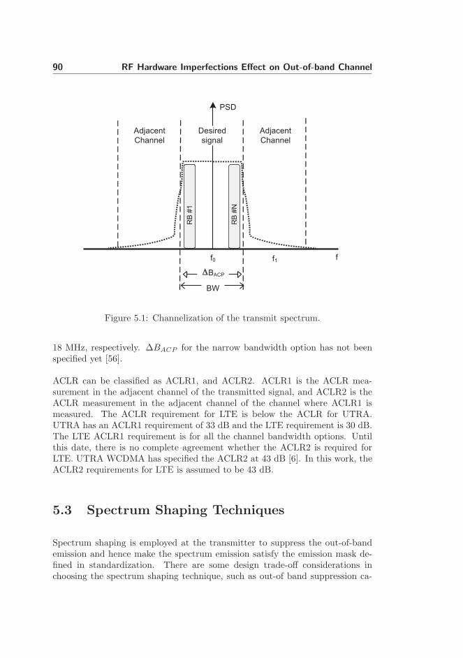
90 RF Hardware Imperfections Effect on Out-of-band Channel
RB
#1
BW
RB
#N
PSD
f
Desired
signal
Adjacent
Channel
Adjacent
Channel
f0 f1
BACP
Figure 5.1: Channelization of the transmit spectrum.
18 MHz, respectively. ∆BACP for the narrow bandwidth option has not beenspecified yet [56].
ACLR can be classified as ACLR1, and ACLR2. ACLR1 is the ACLR mea-surement in the adjacent channel of the transmitted signal, and ACLR2 is theACLR measurement in the adjacent channel of the channel where ACLR1 ismeasured. The ACLR requirement for LTE is below the ACLR for UTRA.UTRA has an ACLR1 requirement of 33 dB and the LTE requirement is 30 dB.The LTE ACLR1 requirement is for all the channel bandwidth options. Untilthis date, there is no complete agreement whether the ACLR2 is required forLTE. UTRA WCDMA has specified the ACLR2 at 43 dB [6]. In this work, theACLR2 requirements for LTE is assumed to be 43 dB.
5.3 Spectrum Shaping Techniques
Spectrum shaping is employed at the transmitter to suppress the out-of-bandemission and hence make the spectrum emission satisfy the emission mask de-fined in standardization. There are some design trade-off considerations inchoosing the spectrum shaping technique, such as out-of band suppression ca-

Spectrum Shaping Techniques 91
DFTNDFT
IFFTNFFT
SC-FDMA with Digital Filter
Over
sampling
L timesS/P
MPSK/
MQAMAdd
CPP/S
Digital
Filter
DFT
NDFT
IFFT
NFFT x L
SC-FDMA with Time Windowing
Time
WindowingS/P
MPSK/
MQAMAdd
CPP/S
Figure 5.2: SC-FDMA transmitter structures with spectrum shaping.
pability, capacity loss, and hardware complexity.
Digital filtering and time windowing are the most commonly used spectrumshaping techniques. Time windowing offers low complexity with the cost of re-duction in the cyclic prefix length due to the signal overlapping [58],[63]. In thiswork, a spectrum shaping technique for LTE UE using an Inverse ChebyshevDigital Infinite Impulse Response (IIR) filter is proposed and evaluated. The fil-ter selection is based on studies in [25] where this filter type achieves minimumcapacity loss. The aim of the study is to propose an IIR digital filter basedspectrum shaping technique for LTE. The performance is compared with thewindowing based spectrum shaping technique, so that the UE spectrum emis-sion mask can be fulfilled for various UE allocated bandwidths with minimumcapacity loss.
5.3.1 IIR Digital Filter
Spectrum shaping can be controlled by means of implementing a digital filterin the transmitter, such as a FIR filter, IIR filter and pulse-shaping. However,the SC-FDMA signal requires a sharp suppression in the transition band in
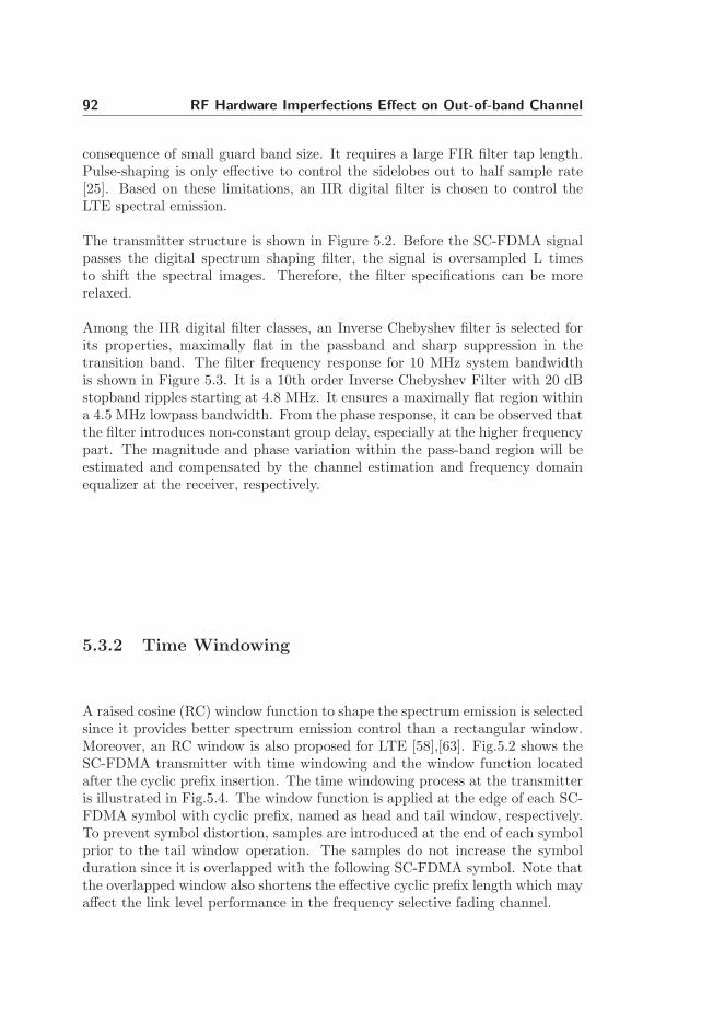
92 RF Hardware Imperfections Effect on Out-of-band Channel
consequence of small guard band size. It requires a large FIR filter tap length.Pulse-shaping is only effective to control the sidelobes out to half sample rate[25]. Based on these limitations, an IIR digital filter is chosen to control theLTE spectral emission.
The transmitter structure is shown in Figure 5.2. Before the SC-FDMA signalpasses the digital spectrum shaping filter, the signal is oversampled L timesto shift the spectral images. Therefore, the filter specifications can be morerelaxed.
Among the IIR digital filter classes, an Inverse Chebyshev filter is selected forits properties, maximally flat in the passband and sharp suppression in thetransition band. The filter frequency response for 10 MHz system bandwidthis shown in Figure 5.3. It is a 10th order Inverse Chebyshev Filter with 20 dBstopband ripples starting at 4.8 MHz. It ensures a maximally flat region withina 4.5 MHz lowpass bandwidth. From the phase response, it can be observed thatthe filter introduces non-constant group delay, especially at the higher frequencypart. The magnitude and phase variation within the pass-band region will beestimated and compensated by the channel estimation and frequency domainequalizer at the receiver, respectively.
5.3.2 Time Windowing
A raised cosine (RC) window function to shape the spectrum emission is selectedsince it provides better spectrum emission control than a rectangular window.Moreover, an RC window is also proposed for LTE [58],[63]. Fig.5.2 shows theSC-FDMA transmitter with time windowing and the window function locatedafter the cyclic prefix insertion. The time windowing process at the transmitteris illustrated in Fig.5.4. The window function is applied at the edge of each SC-FDMA symbol with cyclic prefix, named as head and tail window, respectively.To prevent symbol distortion, samples are introduced at the end of each symbolprior to the tail window operation. The samples do not increase the symbolduration since it is overlapped with the following SC-FDMA symbol. Note thatthe overlapped window also shortens the effective cyclic prefix length which mayaffect the link level performance in the frequency selective fading channel.

Spectrum Shaping Techniques 93
2 2.5 3 3.5 4 4.5 5 5.5 6 6.5 7 7.5
x 106
−80
−60
−40
−20
0
Frequency (MHz)
Mag
nitu
de (
dB)
2 2.5 3 3.5 4 4.5 5 5.5 6 6.5 7 7.5
x 106
−180
−140
−100
−60
−20
20
60
100
140
180
Frequency (MHz)
Pha
se (
degr
ee)
Figure 5.3: Inverse Chebyshev filter frequency response for 10 MHz systembandwidth.
Figure 5.4: Time windowing process of the SC-FDMA symbol.

94 RF Hardware Imperfections Effect on Out-of-band Channel
Table 5.2: LTE uplink Transmission Parameters.
Spectrum Sampling- LB size Max. CP length
Allocation rate #SCs/samples RB samples
20 MHz 30.72 MHz 1200/2048 100 127
15 MHz 23.04 MHz 900/1536 75 95
10 MHz 15.36 MHz 600/1024 50 63
5 MHz 7.68 MHz 300/512 25 31
2.5 MHz 3.84 MHz 144/256 12 15
1.25 MHz 1.92 MHz 72/128 6 7
The raised cosine window function is given by:
w [n] =
12
(1 − cos
(2πn
LNov−1
))n ≤ LNov
1 LNov + 1 ≤ L (NCP + NFFT )12
(1 + cos
(2πn
LNov−1
))n ≥ L (NCP + NFFT ) + 1
(5.2)
Where Nov is the number of overlapped window samples, NCP is the numberof Cyclic Prefix samples, and NFFT is the FFT size.
5.4 Assumptions & Scenarios on Controlling Out-of-band Emission
To compare, and eventually propose a spectrum shaping technique, the twotechniques are evaluated for their ability to control out-of-band emissions. Thespectrum shaping techniques are evaluated using computer based link level sim-ulation. The simulation is performed in accordance with the parameters givenin Table 5.2, and Table 5.3. Each spectrum allocation setting has specific pa-rameters, including the sampling rate, Long Block (LB) symbol size in termsof the useful sub-carriers (SCs) and samples, maximum Resource Block (RB)size, and Cyclic Prefix (CP) length. The minimum UE transmission bandwidthis 1 RB, which contains 12 SCs in 180 kHz bandwidth. The CP duration ismaintained at around 4.1 µs for different spectrum allocation settings.

Assumptions & Scenarios on Controlling Out-of-band Emission 95
Table 5.3: Simulation Parameters.
Parameter Values
Bandwidth 1.25 MHz, 10 MHz
Modulation 16QAM
Oversampling (L) 4
Interpolation Filter 8th order FIR low pass filter
Shaping Filter 10th order Inverse Chebyshev
UE max TX Power 24 dBm
Receiver MMSE receiver
Channel Estimation Linear Interpolation
EVM from Gain Imbalance 4%
EVM from Phase Imbalance 4%
EVM from Nonlinear PA 4%
During the simulation, the spectral emission mask and adjacent channel leakageratio requirements are following the assumptions defined in Section 5.2. The Er-ror Vector Magnitude (EVM) is measured at the receiver symbol detection inputas described in Section 4.2. It allows to perform amplitude/phase equalizationof the unknown transmit filter response. The EVM expresses the error in thereceived constellation diagram and can be used as a direct measure to estimatethe capacity loss as described in Chapter 4. EVM of 4 % is selected as the casestudy, where the typical error levels from each imperfection are created at thatEVM level. The operating point of the nonlinear amplifier is at 24 dBm. It hasbeen chosen so that it is comparable with the WCDMA transmitter operatingat the maximum output power.
The sampling rate for the digital filter method is increased by 4 times using thetime domain interpolation. The interpolation is done by using an 8th order FIRfilter low pass filter. For the time windowing, the sampling rate is also increasedby 4 times using a larger size IFFT operation. Up-conversion with a fixed localoscillator in the center of the frequency band is assumed. For the digital filter,the bandwidth setting is fixed to the system bandwidth in order not to increasethe complexity. It is not practical to set the bandwidth according to the RBsize since the RB size varies from 1 RB up to 1200 RB size. Moreover, The RBsize can be updated in an interval of 1 TTI or 0.5 ms.
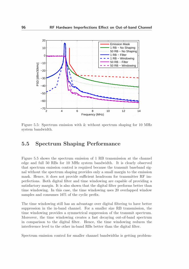
96 RF Hardware Imperfections Effect on Out-of-band Channel
2 4 6 8 10 12 14
x 106
−70
−60
−50
−40
−30
−20
−10
0
10
20
Frequency (MHz)
PS
D [d
Bm
/30k
Hz]
Emission Mask1 RB − No Shaping50 RB − No Shaping1 RB − Filter1 RB − Windowing50 RB − Filter50 RB − Windowing
Figure 5.5: Spectrum emission with & without spectrum shaping for 10 MHzsystem bandwidth.
5.5 Spectrum Shaping Performance
Figure 5.5 shows the spectrum emission of 1 RB transmission at the channeledge and full 50 RBs for 10 MHz system bandwidth. It is clearly observedthat spectrum emission control is required because the transmit baseband sig-nal without the spectrum shaping provides only a small margin to the emissionmask. Hence, it does not provide sufficient headroom for transmitter RF im-perfections. Both digital filter and time windowing are capable of providing asatisfactory margin. It is also shown that the digital filter performs better thantime windowing. In this case, the time windowing uses 20 overlapped windowsamples and consumes 16% of the cyclic prefix.
The time windowing still has an advantage over digital filtering to have bettersuppression in the in-band channel. For a smaller size RB transmission, thetime windowing provides a symmetrical suppression of the transmit spectrum.Moreover, the time windowing creates a fast decaying out-of-band spectrumin comparison to the digital filter. Hence, the time windowing reduces theinterference level to the other in-band RBs better than the digital filter.
Spectrum emission control for smaller channel bandwidths is getting problem-
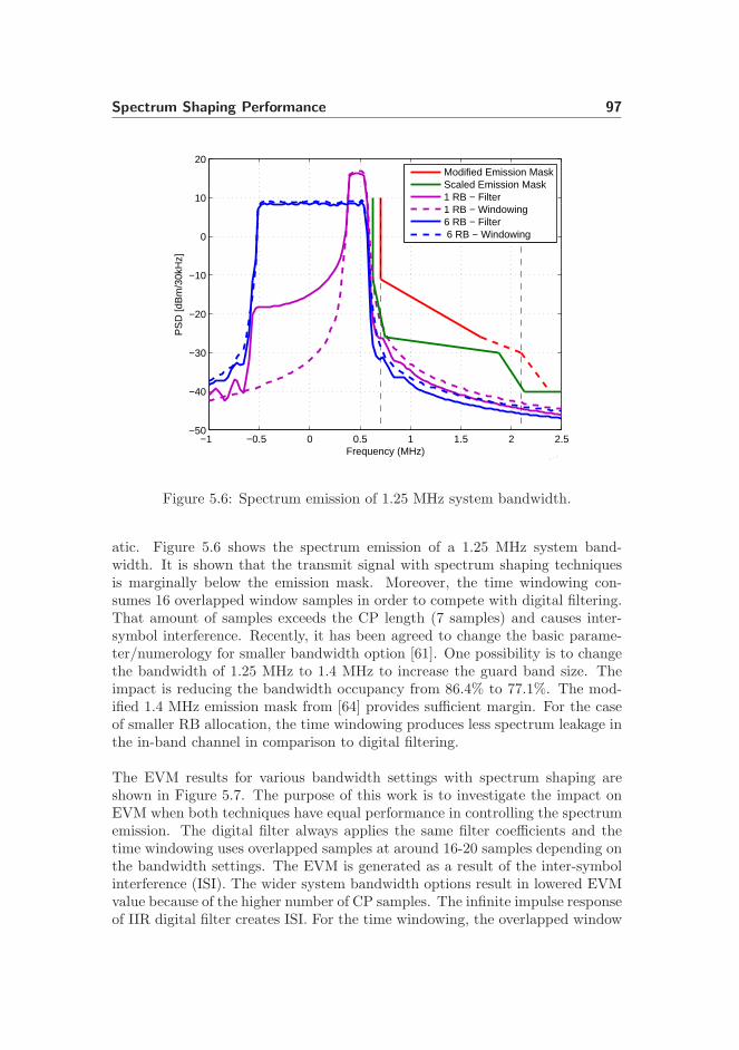
Spectrum Shaping Performance 97
−1 −0.5 0 0.5 1 1.5 2 2.5
x 106
−50
−40
−30
−20
−10
0
10
20
Frequency (MHz)
PS
D [d
Bm
/30k
Hz]
Modified Emission MaskScaled Emission Mask1 RB − Filter1 RB − Windowing6 RB − Filter 6 RB − Windowing
Figure 5.6: Spectrum emission of 1.25 MHz system bandwidth.
atic. Figure 5.6 shows the spectrum emission of a 1.25 MHz system band-width. It is shown that the transmit signal with spectrum shaping techniquesis marginally below the emission mask. Moreover, the time windowing con-sumes 16 overlapped window samples in order to compete with digital filtering.That amount of samples exceeds the CP length (7 samples) and causes inter-symbol interference. Recently, it has been agreed to change the basic parame-ter/numerology for smaller bandwidth option [61]. One possibility is to changethe bandwidth of 1.25 MHz to 1.4 MHz to increase the guard band size. Theimpact is reducing the bandwidth occupancy from 86.4% to 77.1%. The mod-ified 1.4 MHz emission mask from [64] provides sufficient margin. For the caseof smaller RB allocation, the time windowing produces less spectrum leakage inthe in-band channel in comparison to digital filtering.
The EVM results for various bandwidth settings with spectrum shaping areshown in Figure 5.7. The purpose of this work is to investigate the impact onEVM when both techniques have equal performance in controlling the spectrumemission. The digital filter always applies the same filter coefficients and thetime windowing uses overlapped samples at around 16-20 samples depending onthe bandwidth settings. The EVM is generated as a result of the inter-symbolinterference (ISI). The wider system bandwidth options result in lowered EVMvalue because of the higher number of CP samples. The infinite impulse responseof IIR digital filter creates ISI. For the time windowing, the overlapped window

98 RF Hardware Imperfections Effect on Out-of-band Channel
larger than the CP length creates ISI.
Both shaping techniques successfully generate very low EVM for system band-widths equal or greater than 5 MHz. However, the time windowing starts tofail for system bandwidths smaller than 5 MHz. For 2.5 MHz, the overlappedwindow of 16 samples is not just creating an EVM of 1.7%, but also causingthe CP to become useless. It does not serve the actual purpose to absorb theISI due to the frequency selective fading channel. The time windowing becomessignificantly worse for 1.4 MHz system bandwidth option. It requires 16 over-lapped window samples to sufficiently control the spectrum emission and thusgenerates an unacceptable EVM of 16%. Moreover, the overlapped window is129% longer than the CP length. The relation of the number of overlappedwindow samples to the EVM is also shown in Figure 5.7. It can be observedthat increasing the number of overlapped samples increases the EVM. The EVMresult can be improved by reducing the number of overlapped samples at theexpense of unsatisfactory spectrum emission.
5.6 Impact of RF Hardware Imperfections
The capability and effectiveness of the proposed spectrum shaping techniquesin LTE settings with the hardware imperfections are discussed. The impact ofdifferent channel bandwidth and RB size/placement is also studied. The resultsare evaluated based on the margin to the spectrum emission mask and theACLR. The detailed descriptions on the hardware imperfections model used inthis work are given in Chapter 4. To reduce the unwanted emissions, a spectrumshaping technique with IIR digital filter is included in the transmitter based onprevious discussions.
Figure 5.8 shows the impact of a nonlinear amplifier on the spectrum emission ofSC-FDMA and OFDMA. The power amplifier non-linearity model is accordingto Figure. 4.2 and including both AM/AM and AM/PM. The subsequent workalso uses the same PA model. An input back off (IBO) of 4 dB is assumed sothat the generated EVM value is 4%. 16QAM as the highest modulation schemein LTE uplink is used for both SC-FDMA and OFDMA. It is shown that thespectrum emission of OFDMA is marginally below the spectrum emission mask.A better result is obtained for the SC-FDMA transmitter in agreement withPAPR results in Chapter 3.
The ACLR for SC-FDMA with a nonlinear amplifier is shown in Figure 5.9. Theimpact of increasing the input power of a nonlinear amplifier on both QPSK and16QAM is illustrated. The selection of modulation scheme affects the ACLR

Impact of RF Hardware Imperfections 99
8 9 10 11 12 13 14 15 16 17 180
5
10
15
20
25
Overlap Samples
EV
Mrm
s %
Time Windowing || 1.4 MHz System Bandwidth
1.4 2.5 5 10 200
4
8
12
16
20
Bandwidth Settings (x MHz)
EV
Mrm
s %
WindowingDigital Filter
Figure 5.7: EVM results for various bandwidth settings (a) and time windowingwith different overlapped window samples (b).

100 RF Hardware Imperfections Effect on Out-of-band Channel
−0.5 0 0.5 1 1.5 2 2.5 3
x 107
−60
−50
−40
−30
−20
−10
0
10
Frequency (MHz)
PS
D [d
Bm
/30k
Hz]
SC−FDMAOFDMASpectrum Emission Mask
Figure 5.8: Spectrum emission of SC-FDMA & OFDMA.
result. SC-FDMA with QPSK has an ACLR result 1.5 dB lower than SC-FDMA with 16QAM. The results are related to the PAPR results of SC-FDMAin Figure 3.5, where the lower modulation scheme has a better PAPR result.
For OFDMA, the ACLR results are shown in Figure 5.10. Different from theresults of SC-FDMA, the ACLR of OFDMA is not affected by the selection ofmodulation scheme. It is mainly due to the envelope of the OFDM signal whichis not affected by the modulation scheme as shown in the PAPR result in Figure3.5.
The above results show that SC-FDMA has better ACLR performance thanOFDMA. The results for 16QAM are summarized in Figure 5.11. Assuming theinput back off is 4 dB, SC-FDMA has a 3 dB better result than OFDMA forACLR1. For ACLR2 requirement, SC-FDMA has a 1 dB better than OFDMA.
Figure 5.12 shows the spectrum emissions of a transmitter with multiple RFimperfections, such as nonlinear amplifier, gain imbalance, and phase imbalance.The EVM contribution of each RF imperfection is given in Table 5.3. Thecorresponding RF imperfections parameter can be obtained from Figure 4.8.To distinguish the impact of each imperfection, the nonlinear power amplifiercreates spectral regrowth, and the IQ mismatch creates the additional emissionpeaks at the transmission of smaller RB. The impact of IQ mismatch cannot be

Impact of RF Hardware Imperfections 101
−6 −4 −2 0 2 4 6 8 10 12 1415
20
25
30
35
40
45
50
55
Pin
(dBm)
AC
LR (
dB)
16QAMQPSK16QAMQPSK
ACLR 1
ACLR 2
Figure 5.9: ACLR results of SC-FDMA with Nonlinear Amplifier.
−6 −4 −2 0 2 4 6 8 10 12 1415
20
25
30
35
40
45
50
55
Pin
(dBm)
AC
LR (
dB)
16QAMQPSK16QAMQPSK
ACLR 1
ACLR 2
Figure 5.10: ACLR results of OFDMA with Nonlinear Amplifier.

102 RF Hardware Imperfections Effect on Out-of-band Channel
ACLR1 ACLR20
5
10
15
20
25
30
35
40
45
50
AC
LR [d
B]
SC−FDMAOFDMA
Figure 5.11: Summary of SC-FDMA and OFDMA ACLR results.
observed at the large RB allocation. These are the unwanted images which aregenerated by gain and phase imbalances. The IQ mismatch is created before thenonlinear PA. Therefore, the unwanted image also appears as harmonic productsbetween the image and the wanted signal.
Based on the results in Figure 5.12, the spectral emission of both RB allocationsare still below the spectral emission mask assuming that the EVM contributionfrom each imperfection is in the order of 4%. Beside violating the spectrumemission requirement, the hardware imperfections also reduce spectral efficiencyas discussed in the previous chapter.
The ACLR results for the transmitter with the imperfections as given in Table5.3 are illustrated in Figure 5.13. The purpose is to analyze the impact of theRB size and allocation. For the case without the imperfections, the small RBsize at the channel edge has a better result than large RB size transmission.The result for small RB and large RB size is at least 19 dB higher than the LTEACLR1 requirement. The case for the transmitter with imperfections shows theopposite. The ACLR of the transmission with large RB size is worse than thesmall RB size. For the RB size of 50, the ACLR1 is at 33 dB, which is 3dBabove the LTE ACLR1 requirement. The ACLR2 result is also higher than theUTRA ACLR2 requirement (43 dB) by 7 dB.

Impact of RF Hardware Imperfections 103
−0.5 0 0.5 1 1.5 2 2.5 3−60
−50
−40
−30
−20
−10
0
10
20
Frequency (x10 MHz)
PS
D [d
Bm
/30k
Hz]
Emission Mask1 RB − Filter1 RB − Windowing50 RB − Filter50 RB − Windowing
Figure 5.12: Spectrum emission of a transmitter (10 MHz) with imperfectionsas given in Table 5.3.
0 4 8 12 16 20 24 28 32 36 40 44 48
32
36
40
44
48
52
56
60
64
# allocated of RBs
AC
LR (
dB)
ACLR1 (w RF)ACLR2 (w RF)ACLR1 (w/o RF)ACLR2 (w/o RF)
Figure 5.13: ACLR results of a transmitter (10MHz) with and without imper-fections as given in Table 5.3.
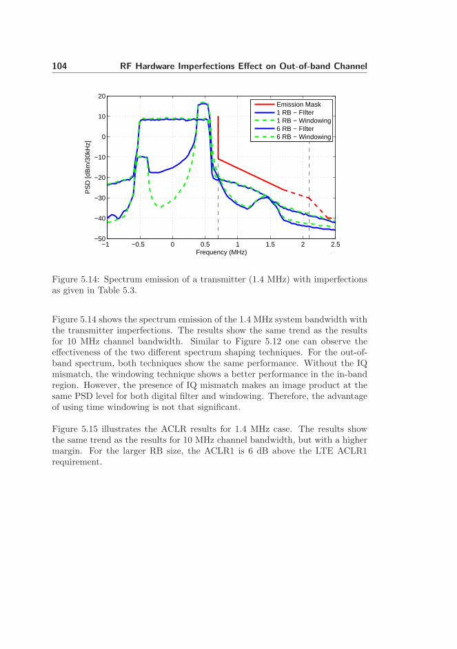
104 RF Hardware Imperfections Effect on Out-of-band Channel
−1 −0.5 0 0.5 1 1.5 2 2.5
x 106
−50
−40
−30
−20
−10
0
10
20
Frequency (MHz)
PS
D [d
Bm
/30k
Hz]
Emission Mask1 RB − FIlter1 RB − Windowing6 RB − FIlter6 RB − Windowing
Figure 5.14: Spectrum emission of a transmitter (1.4 MHz) with imperfectionsas given in Table 5.3.
Figure 5.14 shows the spectrum emission of the 1.4 MHz system bandwidth withthe transmitter imperfections. The results show the same trend as the resultsfor 10 MHz channel bandwidth. Similar to Figure 5.12 one can observe theeffectiveness of the two different spectrum shaping techniques. For the out-of-band spectrum, both techniques show the same performance. Without the IQmismatch, the windowing technique shows a better performance in the in-bandregion. However, the presence of IQ mismatch makes an image product at thesame PSD level for both digital filter and windowing. Therefore, the advantageof using time windowing is not that significant.
Figure 5.15 illustrates the ACLR results for 1.4 MHz case. The results showthe same trend as the results for 10 MHz channel bandwidth, but with a highermargin. For the larger RB size, the ACLR1 is 6 dB above the LTE ACLR1requirement.

Summary 105
1 2 3 4 5 635
37
39
41
43
45
47
49
51
53
55
57
59
# allocated of RBs
AC
LR (
dB)
ACLR1 (w RF)ACLR2 (w RF)ACLR1 (w/o RF)ACLR2 (w/o RF)
Figure 5.15: ACLR results of a transmitter (1.4 MHz) with and without imper-fections.
5.7 Summary
Spectrum shaping techniques for LTE, impact of RF imperfections, and LTE RBsize/placement issues have been discussed in this chapter. LTE has a stringentout-of-band requirements since the UE must be capable of controlling the spec-trum emission for different bandwidth settings. On the other hand, the usageof spectrum shaping techniques must ensure sufficient margin to the spectrumemission mask, acceptable EVM level, minimize the cyclic prefix consumption,and lead to reasonable implementation complexity. The proposed spectrumshaping technique based on a 10th order Inverse Chebyshev filter is capable ofcontrolling the spectral emission for various bandwidth settings, and providesgood trade-off between spectrum emission control, capacity loss minimization,and implementation complexity.
Numerous RF imperfections have been considered in this study. A nonlinearamplifier creates spectral regrowth close to the assigned channel bandwidth,while gain and phase imbalances create unwanted image products. These RFimperfections can violate both the spectrum emission mask and ACLR require-ments. Without the RF imperfections, a small RB size at the channel edgeshows a potential problem to the adjacent channel. In the presence of the hard-

106 RF Hardware Imperfections Effect on Out-of-band Channel
ware imperfections, the impact of large RB size is more severe than the smallRB size. Large RB size shows to produce lower ACLR than the small RB sizetransmission.
Different RB size allocation makes the spectral regrowth affect both the out-of-band channel and the in-band channel. The impact on the in-band channel isthe inter RB interference within the channel bandwidth. This topic is addressedin Chapter 7.

“ Engineering is the professional and systematic appli-cation of science to the efficient utilization of naturalresources to produce wealth. ”
T. J. Hoover and J. C. L. Fish
Chapter 6
Polar Transmitter for LTEUplink
6.1 Introduction
In comparison with WCDMA, an LTE baseband signal has a high Peak-to Av-erage Power Ratio (PAPR). If the RF transmitter architecture relies on a Carte-sian type which typically use a class A or class AB power amplifier, this mayresult in a decrease of power amplifier efficiency. One of the solutions for a bet-ter efficiency is to choose a polar RF transmitter architecture for LTE uplink.A polar transmitter has been successfully implemented in existing wireless com-munication systems, such as GSM [65], EDGE [66], WCDMA [22], and WLANsystem [39]. It can reach an efficiency up to 90% for a CDMA based system[67]. A high efficiency in the polar transmitter can be achieved by employing aswitch mode class E power amplifier.
Beside the promising prospect of achieving high efficiency, the polar transmitteralso suffers from numerous imperfections as described in Section 2.5. In thischapter the impact of polar transmitter imperfections on the beyond 3G systemis investigated. For a case study, the LTE uplink system is considered. Besidea high PAPR, the main challenge is related to the wideband system in LTE.Similar to the previous study, the work is started and focused on the inband
108 Polar Transmitter for LTE Uplink
performance. The aim of this work is to link the individual RF imperfectionEVM characteristics to the link level performance, especially to obtain a clearinsight into the sensitivity of each RF imperfection. The impact of timing delayalignment, power amplifier non-idealities, limited bandwidth on the envelopepath are investigated. The PA non-idealities include the AM/AM distortion,AM/PM distortion, and signal leakage. The link level performance is evaluatedfor AWGN and frequency selective fading channels. Secondly, the work on LTEout-of-band performance is carried out. The polar transmitter imperfectionsare not just degrading the link level performance but also causing a spectralregrowth. Based on these two performance analyses, the most critical imperfec-tions and performance aspects can be identified. Moreover, a polar transmittercan be a solution for the beyond 3G system RF front-end.
This chapter is organized as follows. Section 6.2 reviews the model of imperfec-tions in a polar transmitter architecture for LTE uplink. Section 6.3 describesthe class E PA non-idealities in a polar transmitter. In-band performance eval-uation results of EVM and the impact on link level performance are discussedin Section 6.4. Section 6.5 provides the out-of-band performance results, andfinally a summary is given in Section 6.6.
6.2 Modeling Assumptions
The LTE uplink transmitter with the polar transmitter imperfections model isshown in Figure 6.1. The detailed description of the SC-FDMA baseband signalgeneration and its performance evaluation has been described in chapter 3. TheSC-FDMA signal generator output is up-sampled and filtered to further shiftthe image product as was done previously.
The considered polar transmitter architecture is an Envelope Elimination andRestoration (EER) type as described in Section 2.4. Prior to the RF part, theI & Q signals are converted to the envelope and phase paths in the baseband.This process is a non-linear process. The imperfections model in the EER polartransmitter consists of the timing delay between the envelope and phase paths,limited bandwidth in the envelope path, and the imperfections in the poweramplifier as described in Section 2.5. These are the main polar transmitterimperfections.
The polar transmitter imperfections on LTE uplink performance are evaluatedbased on a link level simulation. The details on the link level processing can befound in Appendix A. The simulation is carried out in accordance with the LTEuplink main parameters given in Table 3.2. During the simulation the following
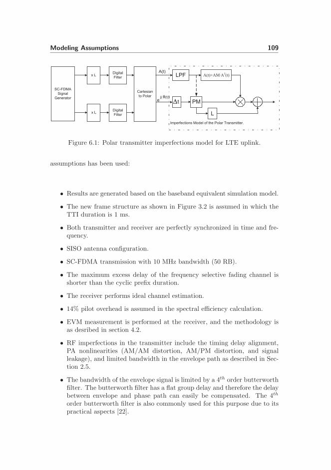
Modeling Assumptions 109
A(t)
ej( (t))
x L
SC-FDMA
Signal
Generator
Digital
Filter
Cartesian
to Polar
x LDigital
Filter
A(t)+AM·A3(t)
PM
L
t
Imperfections Model of the Polar Transmitter.
LPF
Figure 6.1: Polar transmitter imperfections model for LTE uplink.
assumptions has been used:
• Results are generated based on the baseband equivalent simulation model.
• The new frame structure as shown in Figure 3.2 is assumed in which theTTI duration is 1 ms.
• Both transmitter and receiver are perfectly synchronized in time and fre-quency.
• SISO antenna configuration.
• SC-FDMA transmission with 10 MHz bandwidth (50 RB).
• The maximum excess delay of the frequency selective fading channel isshorter than the cyclic prefix duration.
• The receiver performs ideal channel estimation.
• 14% pilot overhead is assumed in the spectral efficiency calculation.
• EVM measurement is performed at the receiver, and the methodology isas desribed in section 4.2.
• RF imperfections in the transmitter include the timing delay alignment,PA nonlinearities (AM/AM distortion, AM/PM distortion, and signalleakage), and limited bandwidth in the envelope path as described in Sec-tion 2.5.
• The bandwidth of the envelope signal is limited by a 4th order butterworthfilter. The butterworth filter has a flat group delay and therefore the delaybetween envelope and phase path can easily be compensated. The 4th
order butterworth filter is also commonly used for this purpose due to itspractical aspects [22].
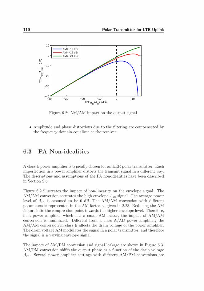
110 Polar Transmitter for LTE Uplink
−40 −30 −20 −10 0 10−40
−30
−20
−10
0
10
20log10
(Ain
) (dB)
20lo
g 10(A
out)
(dB
)
AM=−12 dBrAM=−18 dBrAM=−24 dBr
Figure 6.2: AM/AM impact on the output signal.
• Amplitude and phase distortions due to the filtering are compensated bythe frequency domain equalizer at the receiver.
6.3 PA Non-idealities
A class E power amplifier is typically chosen for an EER polar transmitter. Eachimperfection in a power amplifier distorts the transmit signal in a different way.The descriptions and assumptions of the PA non-idealities have been describedin Section 2.5.
Figure 6.2 illustrates the impact of non-linearity on the envelope signal. TheAM/AM conversion saturates the high envelope Ain signal. The average powerlevel of Ain is assumed to be 0 dB. The AM/AM conversion with differentparameters is represented in the AM factor as given in 2.23. Reducing the AMfactor shifts the compression point towards the higher envelope level. Therefore,in a power amplifier which has a small AM factor, the impact of AM/AMconversion is minimized. Different from a class A/AB power amplifier, theAM/AM conversion in class E affects the drain voltage of the power amplifier.The drain voltage AM modulates the signal in a polar transmitter, and thereforethe signal is a varying envelope signal.
The impact of AM/PM conversion and signal leakage are shown in Figure 6.3.AM/PM conversion shifts the output phase as a function of the drain voltageAin. Several power amplifier settings with different AM/PM conversions are

Inband Performance 111
0 0.5 1 1.5 2 2.5 3−15
−10
−5
0
Ain
(V)
Pha
se s
hift
(deg
ree)
AM/PM= −1 deg/VAM/PM= −3 deg/VAM/PM= −5 deg/V
0 0.5 1 1.5 2 2.5 3−100
−80
−60
−40
−20
0
Ain
(V)
Pha
se s
hift
(deg
ree)
AM/PM = −5 deg/V, L = −28 dBr. θin
= π/2
AM/PM = −5 deg/V, L = −22 dBr. θin
= π/2
AM/PM = −5 deg/V, L = −16 dBr. θin
= π/2
Figure 6.3: AM/PM & signal leakage impact on the output signal.
also illustrated. A power amplifier with high |PM | factor has a large phaseshift. The impact of both AM/PM and signal leakage can also be found. Asignal leakage with initial phase shift of π/2 is assumed [20]. Hence, a low inputsignal provides a phase shift of π/2 corresponding to predominantly capacitiveleakage through the power amplifier.
6.4 Inband Performance
The impact of the polar transmitter imperfections on the in-band channel isanalyzed. In this work the analyses are based on the link level performanceresults on the EVM, spectral efficiency and SNR loss. The methodology issimilar with the work in chapter 4.
Figure 6.4 shows the impact of timing delay imperfection on the maximumachievable spectral efficiency for different modulation and coding schemes (MCS)
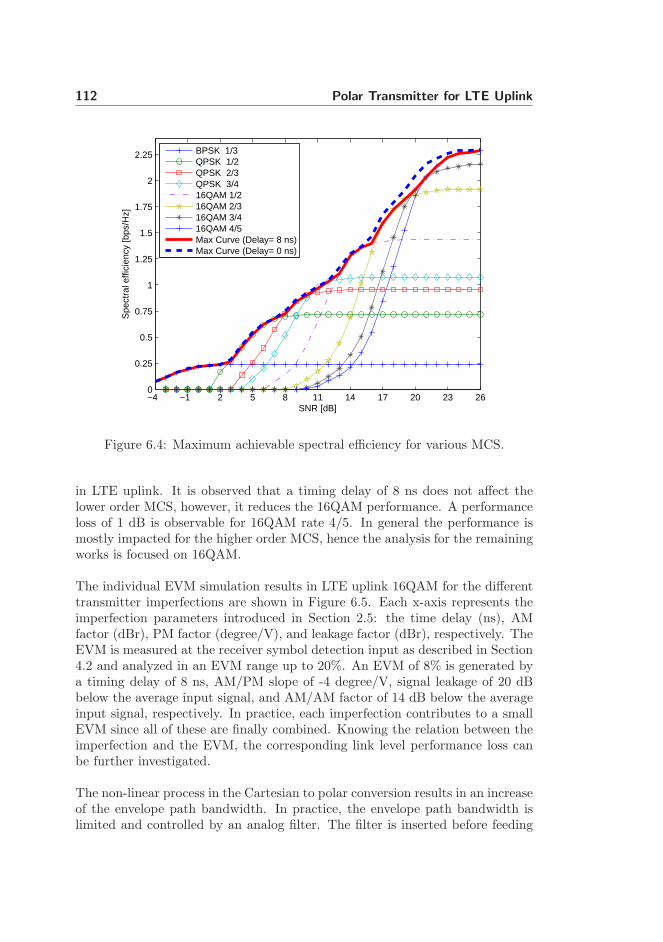
112 Polar Transmitter for LTE Uplink
−4 −1 2 5 8 11 14 17 20 23 260
0.25
0.5
0.75
1
1.25
1.5
1.75
2
2.25
SNR [dB]
Spe
ctra
l effi
cien
cy [b
ps/H
z]
BPSK 1/3QPSK 1/2QPSK 2/3QPSK 3/416QAM 1/216QAM 2/316QAM 3/416QAM 4/5Max Curve (Delay= 8 ns)Max Curve (Delay= 0 ns)
Figure 6.4: Maximum achievable spectral efficiency for various MCS.
in LTE uplink. It is observed that a timing delay of 8 ns does not affect thelower order MCS, however, it reduces the 16QAM performance. A performanceloss of 1 dB is observable for 16QAM rate 4/5. In general the performance ismostly impacted for the higher order MCS, hence the analysis for the remainingworks is focused on 16QAM.
The individual EVM simulation results in LTE uplink 16QAM for the differenttransmitter imperfections are shown in Figure 6.5. Each x-axis represents theimperfection parameters introduced in Section 2.5: the time delay (ns), AMfactor (dBr), PM factor (degree/V), and leakage factor (dBr), respectively. TheEVM is measured at the receiver symbol detection input as described in Section4.2 and analyzed in an EVM range up to 20%. An EVM of 8% is generated bya timing delay of 8 ns, AM/PM slope of -4 degree/V, signal leakage of 20 dBbelow the average input signal, and AM/AM factor of 14 dB below the averageinput signal, respectively. In practice, each imperfection contributes to a smallEVM since all of these are finally combined. Knowing the relation between theimperfection and the EVM, the corresponding link level performance loss canbe further investigated.
The non-linear process in the Cartesian to polar conversion results in an increaseof the envelope path bandwidth. In practice, the envelope path bandwidth islimited and controlled by an analog filter. The filter is inserted before feeding

Inband Performance 113
2 4 6 8 10 12 14 16 18 200
5
10
15
20
25
Time (nsec)
EV
Mrm
s [%
]
Timing alignment
−3 −6 −9 −12 −15 −18 −21 −24 −27 −300
5
10
15
20
25
AM level [dBr]
EV
Mrm
s %
AM/AM
−12−10−8−6−4−200
5
10
15
20
25
PM slope [degree/V]
EV
Mrm
s %
AM/PM
−10 −13 −16 −19 −22 −25 −280
5
10
15
20
25
Leakage [dBr]
EV
Mrm
s %
Leakage
Figure 6.5: EVM results for various polar transmitter imperfections.
the signal to the class E power amplifier. However, inserting a filter also causesadditional timing delay in the envelope path. The additional timing delay hasto be compensated by introducing a similar timing delay in the envelope path.
Figure 6.6 illustrates the impact of limited bandwidth in the envelope path. Thefilter bandwidth is defined as the envelope bandwidth factor multiplied by the3dB bandwidth of the transmitted signal. For 10 MHz channel bandwidth, the3dB bandwidth is 9 MHz. The timing alignment issues have been compensatedso that the error generated is purely as a result of the bandwidth limitation.With a bandwidth factor of 2, the EVM is around 6%. Further increase of thefilter bandwidth reduces the EVM down to 2%. To maintain a low EVM, anenvelope bandwidth factor of at least 3 times is required.
Figure 6.7 shows the spectral efficiency degradation for 16QAM rate 3/4 inconsequence of the signal leakage. The purpose is to observe the impact of theimperfection on the spectral efficiency. The signal leakage imperfection level isdefined by its EVM value. Considering the acceptable target spectral efficiencyloss due to the imperfections is 10%, the corresponding SNR loss for each EVMlevel can be identified. For the low EVM region (< 8%), the SNR loss is lessthan 0.4 dB. The SNR loss significantly increases at the high EVM region. For

114 Polar Transmitter for LTE Uplink
1 1.5 2 2.5 3 3.5 4 4.5 50
2
4
6
8
10
12
14
Envelope BW Factor
EV
Mrm
s (%
)
Figure 6.6: EVM results for limited bandwidth.
an EVM of 16%, the SNR loss is around 1.6 dB. In this analyzes, 16QAM rate3/4 is assumed as the highest order modulation and coding scheme and thereforevery sensitive to the imperfections. For the subsequent work, 16QAM rate 3/4is assumed.
The results in Figure 6.8 illustrate the link level performance by means of equiv-alent SNR degradation of 16QAM rate 3/4 as a result of the RF imperfectionsin an AWGN channel. The SNR loss is plotted versus EVM level. Hence, therelation of performance sensitivity on different imperfections can be obtained.Within the low EVM region (< 8%), all the imperfections have the same SNRloss of less than 0.5 dB. The results are on top of each other, and therefore theEVM is a good direct measure to estimate the link level performance loss withinthis range. At high EVM levels, the SNR loss for each imperfection starts todeviate. Timing delay alignment is more dominant in the SNR loss in compar-ison to the others. The AM/PM distortion and signal leakage show the sameimpact on performance, and the lowest impact is the AM/AM distortion.
Figure 6.9 further shows the relation between the EVM and equivalent SNRloss in the multipath fading channel for 16QAM rate 3/4. A typical Urban 6paths channel model is assumed. The results follow the trend in the AWGNchannel with an increase in the SNR loss range to 4 dB. For the EVM valuesless than 7% - 9%, the SNR loss is maintained below 0.5 dB. The results on thepolar transmitter are in agreement with the previous results on the Cartesian
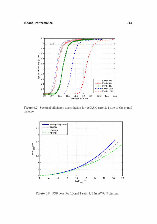
Inband Performance 115
10 10.4 10.8 11.2 11.6 12 12.4 12.8 13.2 13.60
0.2
0.4
0.6
0.8
1
1.2
1.4
1.6
1.8
2
2.2
Average SNR [dB]
Spe
ctra
l Effi
cien
cy [b
ps/H
z]
EVM= 0%EVM= 4%EVM= 8%EVM= 12%EVM= 16%
10%
Figure 6.7: Spectral efficiency degradation for 16QAM rate 3/4 due to the signalleakage.
2 4 6 8 10 12 14 16 18 200
0.5
1
1.5
2
2.5
3
3.5
4
EVMrms
[%]
SN
Rlo
ss [d
B]
Timing alignmentAM/PMLeakageAM/AM
Figure 6.8: SNR loss for 16QAM rate 3/4 in AWGN channel.

116 Polar Transmitter for LTE Uplink
2 4 6 8 10 12 14 16 18 200
0.5
1
1.5
2
2.5
3
3.5
4
EVMrms
[%]
SN
Rlo
ss [d
B]
Timing alignmentAM/PMLeakageAM/AM
Figure 6.9: SNR loss for 16QAM rate 3/4 in TU06 channel.
transmitter in Chapter 4. For 16QAM rate 3/4, an EVM of 8% corresponds toan SNR loss of 0.5 dB. One should note that these results are MCS dependent,as a higher MCS is more sensitive to the EVM.
6.5 Out-of-band Performance
In order to obtain a complete analysis, the impact on the out-of-band spectrumis also studied. The work methodology is similar to the work on the Cartesiantransmitter in Chapter 5. The transmitter structure is shown in Figure 6.1.Before the signal is converted to the polar coordinate system, the signal isoversampled by a raised cosine FIR filter to further shift the image. Afterwards,a spectrum shaping filter is applied to shape the transmit signal. The shapingfilter is an IIR inverse Chebyshev filter as described in Section 5.3.
Figure 6.10 illustrates the impact of timing delay alignment on SC-FDMA spec-trum emission. Timing delay alignment is the most common problem in a polartransmitter. The channel bandwidth is 10 MHz, and the modulation scheme is16QAM. The shaped transmit signal provides a good suppression in the tran-sition band and an excellent margin towards the spectrum emission mask re-quirement. A timing delay of 4 ns is required in order to meet the spectrum
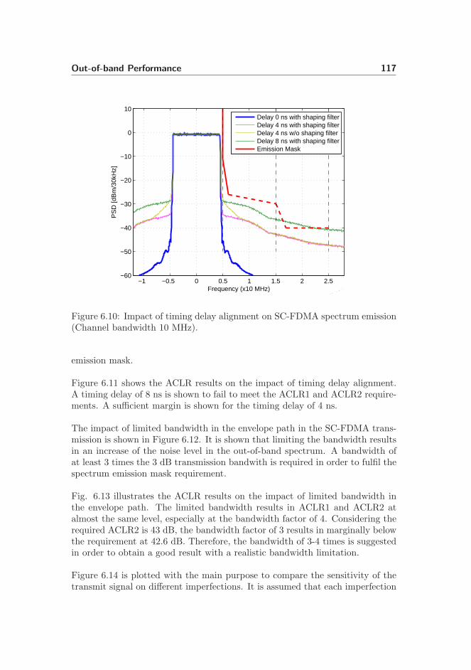
Out-of-band Performance 117
−1 −0.5 0 0.5 1 1.5 2 2.5
x 107
−60
−50
−40
−30
−20
−10
0
10
Frequency (x10 MHz)
PS
D [d
Bm
/30k
Hz]
Delay 0 ns with shaping filterDelay 4 ns with shaping filterDelay 4 ns w/o shaping filterDelay 8 ns with shaping filterEmission Mask
Figure 6.10: Impact of timing delay alignment on SC-FDMA spectrum emission(Channel bandwidth 10 MHz).
emission mask.
Figure 6.11 shows the ACLR results on the impact of timing delay alignment.A timing delay of 8 ns is shown to fail to meet the ACLR1 and ACLR2 require-ments. A sufficient margin is shown for the timing delay of 4 ns.
The impact of limited bandwidth in the envelope path in the SC-FDMA trans-mission is shown in Figure 6.12. It is shown that limiting the bandwidth resultsin an increase of the noise level in the out-of-band spectrum. A bandwidth ofat least 3 times the 3 dB transmission bandwith is required in order to fulfil thespectrum emission mask requirement.
Fig. 6.13 illustrates the ACLR results on the impact of limited bandwidth inthe envelope path. The limited bandwidth results in ACLR1 and ACLR2 atalmost the same level, especially at the bandwidth factor of 4. Considering therequired ACLR2 is 43 dB, the bandwidth factor of 3 results in marginally belowthe requirement at 42.6 dB. Therefore, the bandwidth of 3-4 times is suggestedin order to obtain a good result with a realistic bandwidth limitation.
Figure 6.14 is plotted with the main purpose to compare the sensitivity of thetransmit signal on different imperfections. It is assumed that each imperfection

118 Polar Transmitter for LTE Uplink
55.7
36.8
30.7
63.9
44.4
37.9
0
10
20
30
40
50
60
70
TD=0 ns TD=4 ns TD=8 ns
Timing Delay
AC
LR
(dB
)
ACLR1
ACLR2
Figure 6.11: ACLR results for SC-FDMA with imperfect timing delay align-ment.
−1 −0.5 0 0.5 1 1.5 2 2.5
x 107
−70
−60
−50
−40
−30
−20
−10
0
10
Frequency (x10 MHz)
PS
D [d
Bm
/30k
Hz]
w/o filterFilter BW 4xFilter BW 3xFilter BW 2xEmission Mask
Figure 6.12: Impact of limited bandwidth in the envelope path.

Out-of-band Performance 119
30.5
41
44.2
36.2
42.6
45.2
0
5
10
15
20
25
30
35
40
45
50
BW=2 BW=3 BW=4
Envelope BW
AC
LR
(dB
)ACLR1
ACLR2
Figure 6.13: ACLR results on the limited bandwidth in the envelope path.
generates an EVM of 4%. Timing delay alignment, limited bandwidth of theenvelope signal, and AM/AM conversion are the most severe imperfections.The limited bandwidth is mainly limited by the ACLR2 requirement. AM/AMconversion has a great impact on the ACLR1 result. In practice, timing delayalignment is still the most problematic imperfection because it has to maintainthe delay alignment below 4 ns. Moreover, the ACLR requirement for timingdelay is more stringent than the EVM requirement.

120 Polar Transmitter for LTE Uplink
36.835 34
45.743.144.4
38.8
63 63.1
51.8
0
10
20
30
40
50
60
70
Timing delay Limited BW AM/AM AM/PM Leakage
Imperfections
AC
LR
(dB
)
ACLR1
ACLR2
Figure 6.14: ACLR for different imperfections at EVM=4%.
6.6 Summary
The polar transmitter has a promising prospect of achieving high efficiencypower amplifier. It has been successfully implemented in existing wireless com-munication systems. Beside the advantages, the polar transmitter also suffersfrom numerous imperfections.
In this work the impact of polar transmitter imperfections on LTE uplink per-formance is investigated. The performance of both in-band and out-of-bandare studied. The considered imperfections are the timing delay alignment andnon-ideal power amplifier, and limited bandwidth in the envelope path. TheEVM is a good direct measure to estimate the link level performance loss forvarious imperfections in the practical EVM range (EVM < 8%). For 16QAMrate 3/4, an SNR loss of approximately 0.5 dB can be estimated from an EVMvalue of 8%. The final EVM requirement for the transmitter in LTE will bechosen as a compromise between UE complexity and system performance. Theresults show that the polar transmitter in the LTE uplink is very sensitive to thetiming alignment between the envelope and phase paths, especially for higherorder modulation and coding scheme.
Timing delay alignment, and limited bandwidth in the envelope path are theproblematic imperfections. In practice, the timing delay alignment is the mostdifficult one because it has to control the delay alignment at below 4 ns. Theother imperfections are relatively easier to control. In most cases the out-of-

Summary 121
band requirement are the main limiting factor.

122 Polar Transmitter for LTE Uplink
“ Surround yourself with the best people you can find,delegate authority, and don’t interfere as long as thepolicy you’ve decided upon is being carried out.”
Ronald Reagan
Chapter 7
Inband Inter-User InterferenceAnalysis
7.1 Introduction
UTRA Long Term Evolution has the flexibility to use existing UTRA bandsand new frequency bands [8]. The system supports scalable system bandwidth.On top of that, the user equipment (UE) data transmission is multiplexed infrequency domain, and it has a flexibility to transmit on 1 resource block up to100 RB depending on the resource allocation from the base station. LTE uplinkwith SC-FDMA access scheme offers flexibility for the user to be scheduled inboth frequency and time domain to exploit the radio channel variations [8].
The UE shaping filter controls the transmitted out-of-band spectrum and shouldcomply with the 3GPP standard [68],[69]. Hence, the transmitted signal doesnot interfere with the adjacent channel. However, the in-band signal leakage forsmall RB size transmission remains uncontrolled as discussed in Chapter 5. Inthe ideal condition the SC-FDMA transmission maintains the user orthogonality.However, the presence of hardware imperfections in the RF transceiver, such asfrequency offset and phase noise, destroys the subcarrier orthogonality [70], andthe UE signal leakage start to interfere with other UEs. In practice, the receivedsignals from different UEs experience various frequency offset/phase noise and
124 Inband Inter-User Interference Analysis
lead to the inter-user interference. The power spectral density of the receivedsignals from different UEs may also vary. The different PSD level can be due tothe used modulation and coding rate format, power control inaccuracy, other cellinterference levels, etc [71]. The frequency offset/phase noise and signal leakagefrom the adjacent UEs with higher PSD can lead to a significant interferencelevel and degrade the system performance.
The concept of in-band interference in LTE is first introduced in [72]. In amulti-user environment, the signal leakage and transmitter imperfections fromthe other user can additionally degrade the performance. Ref. [73] shows thatthe in-band unwanted emissions potentially interfere with the other resourceblock.
In this work the impact of the frequency offset/phase noise and different PSDof two interferers on the link level performance of a victim UE for differentresource block allocation is presented. The initial performance evaluation iscarried out based on the error vector magnitude (EVM) measurement. Then,the link level performance in AWGN and Typical Urban channels are performedusing the approach described in [74]. The objective of the work is to relate theSNR degradation of a victim UE as the function of its resource block allocationin various interferer conditions (frequency offset, phase noise and PSD offset).
The chapter is organized as follows. The multi-user modeling scenario is givenin Section 7.2. The interference source is described in Section 7.3. Simulationassumptions in the inter user interference study are discussed in Section 7.3.Finally, the impact of PSD offset and frequency offset are given in Section 7.5.The impact of PSD offset and phase noise is given in Section 7.6. The proposedsolution to deal with inter-user interference is given in Section 7.7. Finally, asummary is given in Section 7.8.
7.2 Description of Multi-user Modeling
The system model of multiple simultaneous UEs transmit to the base-station isillustrated in Figure 7.1. Three active UEs occupy the whole available resouceblock allocation. The two UEs are the interferer UEs, and one UE acts as thevictim UE. The victim UE is allocated in between the interferer UE resourceblock allocation. This configuration will give the worst case scenario for theinterference level to the victim UE.
The performance analysis is based on the performance measurement of the vic-tim UE. The victim UE has an ideal transmission without any RF imperfections.
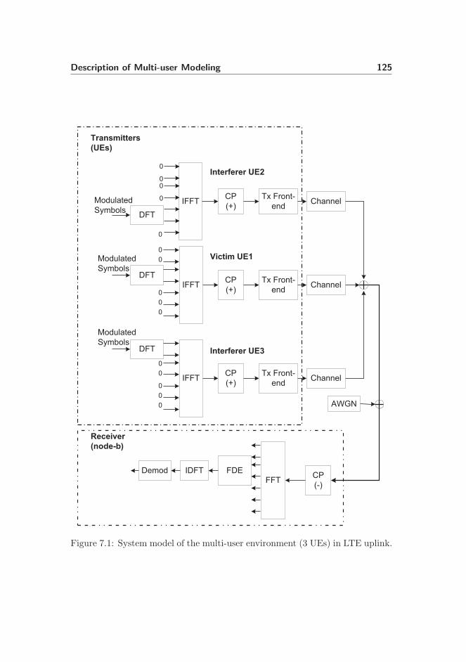
Description of Multi-user Modeling 125
DFT
IFFT
DFT
IFFT
DFT
IFFT
CP
(+)
CP
(+)
ChannelCP
(+)
Channel
Channel
Modulated
Symbols
Modulated
Symbols
Modulated
Symbols
Interferer UE2
Victim UE1
Interferer UE3
0
00
0
0
0
0
0
0
0
0
0
0
0
0
FDE
FFT
IDFTDemod
Tx Front-
end
Tx Front-
end
Tx Front-
end
CP
(-)
Transmitters
(UEs)
Receiver
(node-b)
AWGN
Figure 7.1: System model of the multi-user environment (3 UEs) in LTE uplink.
126 Inband Inter-User Interference Analysis
The transmit signal from the interferer UEs creates interference to the victimUEs. This scenario isolates the performance degradation which is caused onlyby the interference from other users. Only the victim UE signal is processed atthe receiver, and from this the link level performance, i.e. EVM, BLER, spec-tral efficiency, can be evaluated. The EVM is the difference between the idealwaveform and the measured waveform for the allocated RBs and measured atthe receiver symbol detection input as described in Section 4.2.
It has been concluded within 3GPP that the power control is an open-loop powercontrol [75]. In an open-loop power control, a UE adjusts its transmit poweraccording to the downlink pathloss calculated in the UE using the receiveddownlink power level information. In practice, the power control is not perfectdue to the power control measurement error. These conditions lead to thesituation where the average received signal from different UEs has a differentaveraged PSD. Besides, LTE supports various modulation and coding scheme(MCS) [8]. Depending on the SNR level at the receiver, the UE with betterSNR uses high-order MCS and vice-versa.
The average PSD of the simultaneously received signals from the 3 UEs is illus-trated in Figure 7.2. Since the UE can transmit at different resource block size,the receiver does not just measure the power level, but also the averaged PSD[75]. Fig. 7.2 also illustrates a different resource block size among the UEs. Theinterferer UE has a frequency offset, foff , and the average PSD is higher thanthe victim UE. The average PSD difference between interferer UEs and victimUE is denoted as PSD offset, Poff .
In ideal conditions the UE signal leakage to the adjacent resource block is theSINC responses, and the subcarrier orthogonality can still be preserved. There-fore it is not sufficient to analyze the impact of the signal leakage only from thepower spectral density, which is typically obtained from a spectrum analyzer.The analysis should be based on the demodulated signal of the subcarriers withinvictim resource block. However, the power spectral density analysis can still beused to analyze the impact to the out-of-band spectrum or the adjacent channel[76].
7.3 Interference Sources
RF imperfections in the UE interferer can create interference to the victim UE.Frequency offset and phase noise can destroy the subcarriers orthogonality in theSC-FDMA system. Therefore, it is expected that the impact of the frequencyoffset and phase noise has greater impact in terms of interference on the victim

Interference Sources 127
UE 2 UE 1 UE 3PS
D(d
Bm
/Hz)
10 MHz (50 RBs)
Poff
foff foff f
RB
#1
RB
#5
0
Interferer UEs
Victim UE
PNPN
Figure 7.2: Received Power Spectral Density (PSD) of 3 UEs at the base-station.
UE, compared to the other imperfections. Beside the frequency offset and phasenoise, the spectral regrowth generated by the nonlinear amplifier of the interfererUEs can also interfere to the victim UE. In this work, the impact of frequencyoffset and phase noise on the interferer UEs are studied.
The phase noise increases the signal leakage of the UE interferer transmit signal.This effect can destroy the orthogonality of the victim UE subcarriers, especiallythe subcarriers which are close to the interferer UE. A common frequency off-set at the receiver can be corrected by a frequency offset compensation at thereceiver. However, a specific frequency offset at the transmitter has alreadycreated interference with the other users and it should be kept at a minimum.The 3GPP release 7 specifies which the transmitter frequency accuracy shouldbe less than 0.01 ppm, corresponds to 200 Hz of frequency offset [68]. Moreover,each UE has different mobility and results in different Doppler frequency shift.These factors lead to the situation where the received signal from different UEshas various and unequal frequency offsets.
The interferer UEs signal affected by the frequency offset and phase noise canbe expressed in the following equation:
y(t)UEn= x(t) · ej(2πfoff t+φ(t)) (7.1)
where foff represents the frequency offset, and φ(t) is the phase noise.
128 Inband Inter-User Interference Analysis
7.4 Modeling Assumptions
A multi-user link level simulation is carried out to investigate the in-band inter-ference. The simulation is carried out in accordance with the LTE uplink mainparameters given in Table 7.2. The details on the link level processing can befound in Appendix A. The system bandwidth of 10 MHz corresponding to 50RBs, is considered and shared among the UEs. In case the victim UE has asmall RBs allocation, the remaining RBs are shared among the interferer UEs.During the simulation the following assumptions are considered:
• The victim UE transmitter is perfectly synchronized with receiver in timeand frequency.
• The interferer UEs have the same PSD level.
• The interferer UEs have the same absolute frequency offset and phasenoise level.
• The maximum excess delay of the frequency selective fading channel isshorter than the cyclic prefix duration.
• One sub-frame/TTI consists of 12 Long Blocks (LBs) for data and 2 LBsfor reference signals (14% overhead).
The frequency offset is assumed in the worst condition between 200 Hz - 800 Hz.The frequency offset can be generated as the frequency error in the transmitterand the doppler frequency due to the fast moving UE. For simplicity in thiswork, these frequency offset sources are analyzed as a single frequency offset,Foff , generated at the interferer UE transmitter.
The phase noise follows the model described in Section 2.3. Several phase noisepowers are considered based on the SSB phase noise power at 1 MHz frequencyoffset from the carrier. These phase noise powers can be related to the phasenoise bandwidth using (2.13). The phase noise characteristics for this simulationare summarized in Table 7.1. The phase noise type A is to represent the localoscillator which is typically used in the existing GSM/WCDMA system. It maybe useful to characterize the quality of an oscillator by the relation between itsphase noise bandwidth and the subcarrier spacing of the LTE signal (∆fsc):
ρPN =∆f3dB
∆fsc(7.2)
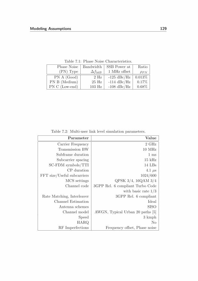
Modeling Assumptions 129
Table 7.1: Phase Noise Characteristics.
Phase Noise Bandwidth SSB Power at Ratio(PN) Type ∆f3dB 1 MHz offset ρPN
PN A (Good) 2 Hz -125 dBc/Hz 0.013%PN B (Medium) 25 Hz -114 dBc/Hz 0.17%PN C (Low-end) 103 Hz -108 dBc/Hz 0.68%
Table 7.2: Multi-user link level simulation parameters.
Parameter Value
Carrier Frequency 2 GHz
Transmission BW 10 MHz
Subframe duration 1 ms
Subcarrier spacing 15 kHz
SC-FDM symbols/TTI 14 LBs
CP duration 4.1 µs
FFT size/Useful subcarriers 1024/600
MCS settings QPSK 3/4, 16QAM 3/4
Channel code 3GPP Rel. 6 compliant Turbo Code
with basic rate 1/3
Rate Matching, Interleaver 3GPP Rel. 6 compliant
Channel Estimation Ideal
Antenna schemes SISO
Channel model AWGN, Typical Urban 20 paths [5]
Speed 3 kmph
HARQ No
RF Imperfections Frequency offset, Phase noise
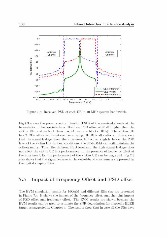
130 Inband Inter-User Interference Analysis
−1.2 −1 −0.8 −0.6 −0.4 −0.2 0 0.2 0.4 0.6 0.8 1 1.2
x 107
−100
−90
−80
−70
−60
−50
−40
−30
−20
−10
0
Frequency (x10 MHz)
PS
D (
dBm
/30
kHz)
UE2 (Interferer)UE1 (Victim)UE3 (Interferer)
AdjacentChannel
AdjacentChannel
Figure 7.3: Received PSD of each UE in 10 MHz system bandwidth.
Fig.7.3 shows the power spectral density (PSD) of the received signals at thebase-station. The two interferer UEs have PSD offset of 20 dB higher than thevictim UE, and each of them has 24 resource blocks (RBs). The victim UEhas 2 RBs allocated in-between interfering UE RBs allocations. It is shownthat the signal leakage from the interferers UE is just slightly below the PSDlevel of the victim UE. In ideal conditions, the SC-FDMA can still maintain theorthogonality. Thus, the different PSD level and the high signal leakage doesnot affect the victim UE link performance. In the presence of frequency offset atthe interferer UEs, the performance of the victim UE can be degraded. Fig.7.3also shows that the signal leakage in the out-of-band spectrum is suppressed bythe digital shaping filter.
7.5 Impact of Frequency Offset and PSD offset
The EVM simulation results for 16QAM and different RBs size are presentedin Figure 7.4. It shows the impact of the frequency offset, and the joint impactof PSD offset and frequency offset. The EVM results are shown because theEVM results can be used to estimate the SNR degradation for a specific BLERtarget as suggested in Chapter 4. The results show that in case all the UEs have

Impact of Frequency Offset and PSD offset 131
0 5 10 15 20 25 300
0.51
1.52
2.53
3.54
4.5
Number of RBs
EV
Mrm
s (%
)
F
offset = 200 Hz
Foffset
= 400 Hz
Foffset
= 800 Hz
0 5 10 15 20 25 300
2
4
6
8
10
12
14
Number of RBs
EV
Mrm
s (%
)
F
offset = 200 Hz
Foffset
= 400 Hz
Foffset
= 800 Hz
Poffset
= 0 dB
Poffset
= 10 dB
Figure 7.4: EVM results at different PSD level and frequency offset for differentRB size.
the same PSD level (Poff = 0), the EVM level is very low. For the frequencyoffset of 800 Hz and victim UE with 1 RB, the EVM level is only 4.5%. TheEVM becomes higher when the PSD offset of the UE interferer is increased.This result is expected because increasing the PSD offset will increase the non-orthogonal signal leakage power level which falls in the allocated frequency ofthe victim UE. The results also show that the smaller RB size obtains higherEVM than the larger RB size.
Figure 7.5 shows the BLER results for a transmission of 5 RBs in an AWGNchannel. It is observed that the frequency offset in combination with the PSDoffset leads to the performance degradation. Considering the target BLER is10%, the SNR loss for the interferer UEs with a frequency offset of 200 Hz andPSD offset of 10 dB is very small, less than 0.1 dB. Increasing the PSD offsetby another 10 dB results in an SNR loss of 0.3 dB.
In Figure 7.6, the degradation of the link level performance by means of equiv-alent SNR degradation at 10% BLER for QPSK rate 3/4 and 16QAM rate 3/4
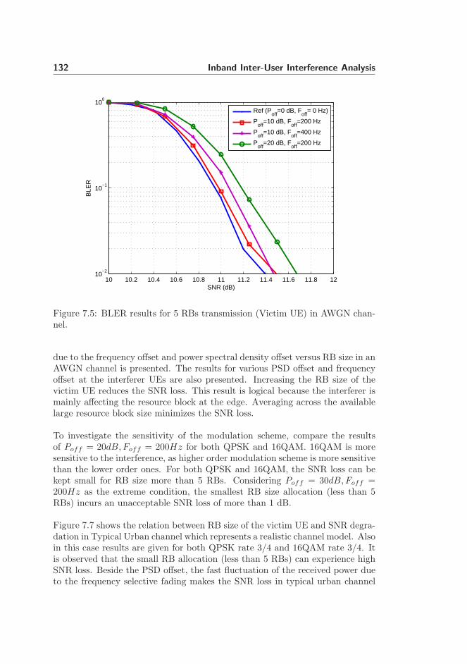
132 Inband Inter-User Interference Analysis
10 10.2 10.4 10.6 10.8 11 11.2 11.4 11.6 11.8 1210
−2
10−1
100
SNR (dB)
BLE
R
Ref (P
off=0 dB, F
off= 0 Hz)
Poff
=10 dB, Foff
=200 Hz
Poff
=10 dB, Foff
=400 Hz
Poff
=20 dB, Foff
=200 Hz
Figure 7.5: BLER results for 5 RBs transmission (Victim UE) in AWGN chan-nel.
due to the frequency offset and power spectral density offset versus RB size in anAWGN channel is presented. The results for various PSD offset and frequencyoffset at the interferer UEs are also presented. Increasing the RB size of thevictim UE reduces the SNR loss. This result is logical because the interferer ismainly affecting the resource block at the edge. Averaging across the availablelarge resource block size minimizes the SNR loss.
To investigate the sensitivity of the modulation scheme, compare the resultsof Poff = 20dB, Foff = 200Hz for both QPSK and 16QAM. 16QAM is moresensitive to the interference, as higher order modulation scheme is more sensitivethan the lower order ones. For both QPSK and 16QAM, the SNR loss can bekept small for RB size more than 5 RBs. Considering Poff = 30dB, Foff =200Hz as the extreme condition, the smallest RB size allocation (less than 5RBs) incurs an unacceptable SNR loss of more than 1 dB.
Figure 7.7 shows the relation between RB size of the victim UE and SNR degra-dation in Typical Urban channel which represents a realistic channel model. Alsoin this case results are given for both QPSK rate 3/4 and 16QAM rate 3/4. Itis observed that the small RB allocation (less than 5 RBs) can experience highSNR loss. Beside the PSD offset, the fast fluctuation of the received power dueto the frequency selective fading makes the SNR loss in typical urban channel

Impact of Frequency Offset and PSD offset 133
0 5 10 15 20 25 300
0.5
1
1.5
2
Number of RBs
SN
Rlo
ss (
dB)
P
off=20 dB, F
off=200 Hz
Poff
=10 dB, Foff
=800 Hz
Poff
=20 dB, Foff
=400 Hz
Poff
=30 dB, Foff
=200 Hz
0 5 10 15 20 25 300
0.5
1
1.5
2
Number of RBs
SN
Rlo
ss (
dB)
P
off=10 dB, F
off=200 Hz
Poff
=10 dB, Foff
=400 Hz
Poff
=20 dB, Foff
=200 Hz
QPSK 3/4
16QAM 3/4
Figure 7.6: Frequency offset and PSD effects (SNRloss)to the in-band interfer-ence in AWGN channel for different RB size
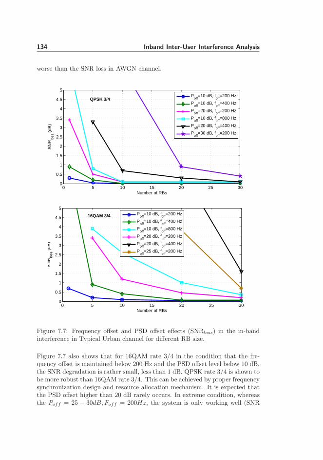
134 Inband Inter-User Interference Analysis
worse than the SNR loss in AWGN channel.
0 5 10 15 20 25 300
0.5
1
1.5
2
2.5
3
3.5
4
4.5
5
Number of RBs
SN
Rlo
ss (
dB)
P
off=10 dB, f
off=200 Hz
Poff
=10 dB, foff
=400 Hz
Poff
=20 dB, foff
=200 Hz
Poff
=10 dB, foff
=800 Hz
Poff
=20 dB, foff
=400 Hz
Poff
=30 dB, foff
=200 Hz
0 5 10 15 20 25 300
0.5
1
1.5
2
2.5
3
3.5
4
4.5
5
Number of RBs
SN
Rlo
ss (
dB)
P
off=10 dB, f
off=200 Hz
Poff
=10 dB, foff
=400 Hz
Poff
=10 dB, foff
=800 Hz
Poff
=20 dB, foff
=200 Hz
Poff
=20 dB, foff
=400 Hz
Poff
=25 dB, foff
=200 Hz
QPSK 3/4
16QAM 3/4
Figure 7.7: Frequency offset and PSD offset effects (SNRloss) in the in-bandinterference in Typical Urban channel for different RB size.
Figure 7.7 also shows that for 16QAM rate 3/4 in the condition that the fre-quency offset is maintained below 200 Hz and the PSD offset level below 10 dB,the SNR degradation is rather small, less than 1 dB. QPSK rate 3/4 is shown tobe more robust than 16QAM rate 3/4. This can be achieved by proper frequencysynchronization design and resource allocation mechanism. It is expected thatthe PSD offset higher than 20 dB rarely occurs. In extreme condition, whereasthe Poff = 25 − 30dB, Foff = 200Hz, the system is only working well (SNR
Impact of Phase Noise and PSD Offset 135
loss less than 1 dB) when a larger RB size is used by the victim UE (RB size=30).
7.6 Impact of Phase Noise and PSD Offset
Figure 7.8 shows the impact of phase noise on the inband interference for dif-ferent RB size. The results are for AWGN channel scenario so that the sourceof the performance degradation can be narrowed down to the AWGN noise andthe interference from neighboring users. A good (PN-A) and a medium (PN-B)quality local oscillator are assumed. In most cases, the SNR loss can be keptvery low for both QPSK rate 3/4 and 16QAM rate 3/4, except for a very smallRB size and at the extreme condition (Poff = 30dB).
To show the results in a realistic channel, the SNR loss versus the RB size isplotted and shown in Figure 7.9. The results presented are for various PSDoffsets and phase noise types. In general, the results follow the trend in theAWGN channel results. The results in a typical urban channel have a largescale of SNR loss. In most of the cases, the SNR loss can be maintained low forboth QPSK rate 3/4 and 16QAM rate 3/4, especially for a large RB size (RBsize ≥ 5). In extreme conditions in which the (Poff = 30dB, PN type A), thesystem can still work well for QPSK with RB size ≥ 5 and for 16QAM rate 3/4is only for RB size ≥ 30.
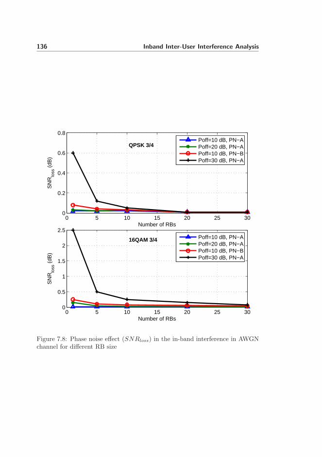
136 Inband Inter-User Interference Analysis
0 5 10 15 20 25 300
0.2
0.4
0.6
0.8
Number of RBs
SN
Rlo
ss (
dB)
Poff=10 dB, PN−APoff=20 dB, PN−APoff=10 dB, PN−BPoff=30 dB, PN−A
0 5 10 15 20 25 300
0.5
1
1.5
2
2.5
Number of RBs
SN
Rlo
ss (
dB)
Poff=10 dB, PN−APoff=20 dB, PN−APoff=10 dB, PN−BPoff=30 dB, PN−A
QPSK 3/4
16QAM 3/4
Figure 7.8: Phase noise effect (SNRloss) in the in-band interference in AWGNchannel for different RB size
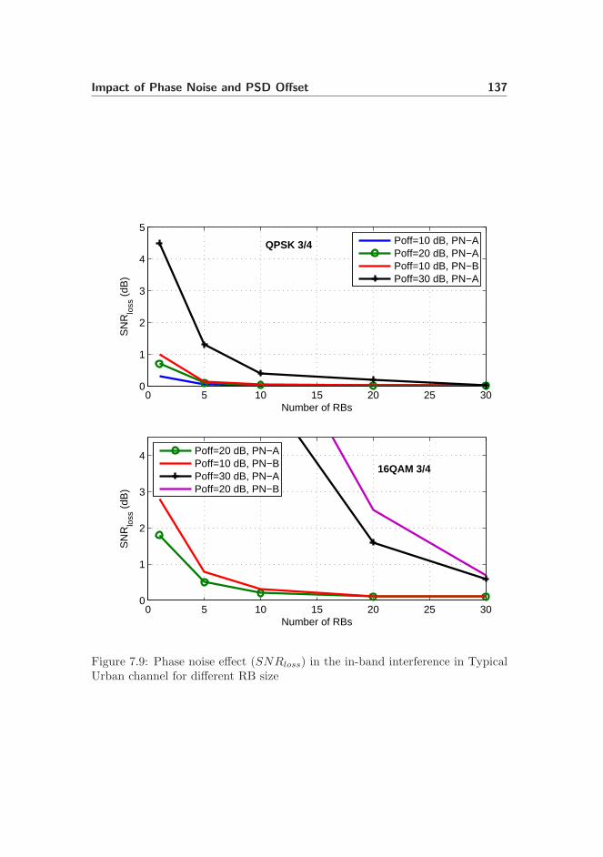
Impact of Phase Noise and PSD Offset 137
0 5 10 15 20 25 300
1
2
3
4
5
Number of RBs
SN
Rlo
ss (
dB)
Poff=10 dB, PN−APoff=20 dB, PN−APoff=10 dB, PN−BPoff=30 dB, PN−A
0 5 10 15 20 25 300
1
2
3
4
Number of RBs
SN
Rlo
ss (
dB)
Poff=20 dB, PN−APoff=10 dB, PN−BPoff=30 dB, PN−APoff=20 dB, PN−B
QPSK 3/4
16QAM 3/4
Figure 7.9: Phase noise effect (SNRloss) in the in-band interference in TypicalUrban channel for different RB size

138 Inband Inter-User Interference Analysis
PS
D(d
Bm
/Hz)
f
RB
#1
RB
#5
0
Cluster 1
Cluster 2Cluster 3
Figure 7.10: UE frequency domain scheduling solution to avoid large PSD offset
7.7 Proposed Solution
From the above analysis, the system can work well if the RF imperfections,such as the frequency offset and phase noise, can be kept low. For instance, thefrequency offset below 200 Hz and a good quality local oscillator (phase noisetype-A). In most cases those imperfections can be controlled by the selection ofgood components for the transmitter. The only remaining factor is to controlthe PSD offset, especially to avoid the victim UEs between the interferer UEsat larger RB size. A solution to avoid this scenario is to schedule the users inthe frequency domain based on the PSD level as shown in Fig.7.10. The usersare clustered based on the measured PSD at the receiver. The users with thehighest PSD are allocated in a cluster and separated away from the users withthe lowest PSD. Therefore, a significant PSD offset between adjacent users canbe avoided. However, it will cost on the degree of freedom of the users schedulingin frequency domain.
7.8 Summary
The impact of in-band interference on the uplink multiple access of beyond 3Gsystem has been investigated. The LTE system parameters are considered as thecase study. In-band and out-of-band interference arise as a result of transmitterimperfections. Out-of-band, or adjacent channel, interference can be controlledby a spectral shaping filter. However, the shaping filter is unable to control the
Summary 139
leakage within the system bandwidth, and the resulting leakage can interferewith other users’ transmission in the uplink multiple access. The interferencefrom the other users is mainly due to the frequency offset and phase noise at thetransmitter and potential differences in power spectral density of the receivedsignals from multiple UEs. The effect of RF imperfections and different PSDlevel from the UE interferers to a victim UE are investigated.
The impact on different UE resource block size allocation is also investigated.The situation is emphasized when the resource block allocation, and hence thebandwidth of the transmitted signal, is small, and when the interfering signal isreceived at higher power spectral density (PSD). Results obtained from an LTEuplink link level simulation show a significant SNR degradation for the victimUE with smaller resource block allocation, especially in realistic propagationchannels. Considering that the frequency offset can be maintained below 200Hz and the PSD offset below 10 dB, the SNR loss is less than 1 dB. Thiscan be achieved by proper frequency synchronization design and resource blockallocation mechanism.
The radio resource management (RRM) mechanism should be aware of placingthe UE frequency allocation to avoid significant SNR degradation, especially forthe UE with small RB size. One possibility to reduce the impact of in-bandinterference is to allocate the UE resource blocks based on the PSD level.

140 Inband Inter-User Interference Analysis

“ When the effective leader is finished with his work,the people say it happened naturally. .”
Lao Tse
Chapter 8
Conclusion
The suitability of beyond 3G systems air interfaces with user equipment hard-ware imperfections has been studied in this dissertation. As a case study, theUTRA LTE uplink is assumed. The analysis is based on the results from a linklevel simulation. The work presented was started with the baseline performanceevaluation of LTE uplink. Several prominent techniques in LTE uplink havebeen considered, such as radio access techniques, link adaptation, H-ARQ, andturbo equalizer. Afterwards, the impact of hardware imperfections on both in-band and out-of-band performance have been investigated. The performanceand requirements aspects in consequence of the imperfections are discussedthroughout the remaining dissertation.
Overall, the results and discussions in this study provide a link between systemlevel design and RF design. System level design is mainly dealing with the spec-tral efficiency and the required signal to noise ratio (SNR), whereas RF designdeals with Error Vector Magnitude (EVM), Adjacent Channel Leakage Ratio(ACLR), and spectrum emission mask (SEM) requirements. In this chapter,the main findings of the PhD study, recommendations, and future work aresummarized.
142 Conclusion
8.1 Main Findings and Contributions
SC-FDMA and OFDMA are the salient air interface for the uplink B3G/4G sys-tems. Baseline performance of both air interfaces combined with the key tech-niques in wireless communication has been analyzed. Both air interfaces havebeen proven to achieve high spectral efficiency. It is shown that the proposedSC-FDMA with turbo equalizer can further improve the BLER performance upto 1 dB in comparison to SC-FDMA with MMSE receiver. SC-FDMA can takeadvantage over OFDMA in cases where the lower order modulation schemesare selected. SC-FDMA achieves a significantly lower PAPR while OFDMA isnot affected by the selection of modulation scheme. SC-FDMA with π/2 BPSKachieves PAPR 4 dB lower than OFDMA. Therefore, the UE can operate at highpower and hence increase the cell coverage. Moreover, a lower PAPR results ina reduced back-off to maximize the power amplifier efficiency.
The most common RF imperfections in the Cartesian transmitter, such as non-linear power amplifier, gain imbalance, phase imbalance, DC offset and phasenoise, have been investigated. The nonlinear power amplifier is the foremostimperfection because it may affect the performance (in-band and out-of-band),the power usage, and the cell coverage. Considering the presence of nonlinearpower amplifier, SC-FDMA is in favor in comparison to OFDMA as a result ofthe lower PAPR. For 16QAM 4/5, SC-FDMA has a better performance by 0.7dB than OFDMA. Moreover, SC-FDMA provides a good balance between theperformance loss and meeting the RF requirements (SEM & ACLR).
Similar investigations on the impact of RF imperfections for the Polar EERtransmitter have been carried out. Timing delay alignment between the envelopeand phase paths is shown to be the most problematic imperfection to meetthe in-band and out-of band requirements. To maintain acceptable in-bandrequirements, the timing delay alignment must be below 8 ns, while the timingdelay alignment of 4 ns is required to meet out-of-band requirements. Otherimperfections, such as limited bandwidth in the envelope path and non-idealclass E power amplification are relatively easy to control.
The relation among individual RF imperfections on LTE uplink performancefor both Cartesian and Polar EER RF transmitters has been presented. Fromthis study, the EVM generated by each imperfection can be associated withthe corresponding link level performance in both AWGN and realistic mobilepropagation (typical urban) channel. The EVM has been shown as a gooddirect measure to estimate the link level performance loss in the practical EVMrange. For 16 QAM, the practical EVM range is around 8 %. Furthermore,an analytical derivation relating the performance loss as result of white noisesource to the EVM level shows a good match with the simulation result. The
Recommendations 143
simulation effort on the impact of RF imperfections on in-band performance canbe further simplified by including a white noise source as an equivalent modelof the RF transmitter imperfections.
A spectrum shaping technique based on a 10th order Inverse Chebyshev filterhas been proposed to control LTE spectrum emission. The proposed techniqueis capable of controlling the spectral emission for various bandwidth settingsand provides a good trade-off between spectrum emission control, capacity lossminimization, and implementation complexity. The spectrum shaping is onlycapable of controlling the out-of-band spectrum, and thus in-band inter-userinterference potentially exists. Therefore, also the impact of in-band interferenceon the LTE uplink has been scrutinized. Considering that the RF imperfectionssuch as frequency offset and phase noise are under control and the PSD offsetbelow 10 dB, the SNR loss for 16QAM 3/4 is less than 1 dB.
8.2 Recommendations
In general, both SC-FDMA and OFDMA air interfaces are suitable for uplinkbeyond 3G systems. SC-FDMA is the preferred selection for the system de-ployment which requires large scale coverage. SC-FDMA in combination witha lower order modulation shows a significantly lower PAPR than OFDMA. Fora small cell coverage in which the system operates at high SNR, OFDMA ispreferred to SC-FDMA. At high SNR, where both air interfaces operate withhigh order modulation, SC-FDMA does not take a significant advantage overOFDMA in terms of PAPR.
The impact of RF transmitter imperfections must be evaluated through bothin-band and out-of-band requirements. Meeting the out-of-band requirements istypically the limiting factor, but the inband performance becomes the limitingfactor for higher order modulation. Higher order modulation has a small EVMrequirement which is hard to achieve.
The EVM measurement results can be used to estimate the performance loss,especially in the practical EVM range. A white noise source as an equivalentmodel of the RF transmitter imperfections can be used to investigate the per-formance loss and hence simplify the investigations. However, it is strictly onlyfor in-band performance. The impact on the out-of band should be evaluatedbased on each RF transmitter imperfection.
The Radio Resource Management should be aware of placing the UE resourceblock allocation to avoid any significant SNR loss. One possibility is to allocate

144 Conclusion
the UE resource block based on the PSD level. However, such a solution willcost on the degree of freedom of the user allocation in the frequency domain.
8.3 Future Work
There are some issues which have not been addressed in this PhD study. Thus,the work can still be extended to the following potential topics.
The impact of RF hardware imperfections on beyond 3G system is investigatedbased on a link level simulation. It would be interesting to assess the impact ofimperfections from the real hardware measurements. There are some practicalissues which can also be investigated from the hardware measurements. Inves-tigation on the impact of power amplifier is still the most important topics.Especially, the capability of the power amplifier to deal with the LTE uplinkwhich has a wide band bandwidth. Moreover, the actual power amplifier effi-ciency obtained from the measurements can be further investigated. However,this work requires at least the availability of the following parts: an LTE uplinkbaseband signal generation, RF transceiver, and the measurement equipments.
The study presented is mainly focused on the impact of the hardware imper-fections for a single antenna configuration. Beyond 3G systems also considerto use multiple-antennas at the transmitter to further enhance the spectral ef-ficiency. There are two scenarios: multiple antennas by combining with otheruser equipments antennas to form a virtual MIMO and multiple antennas inone user equipment. The Virtual MIMO scenario is suitable for a portable userequipment while the other scenario is for a larger user equipment to maintainsufficient distance among antennas. Investigating the impact of hardware im-perfections on a multiple-antenna configuration is also a prominent topic. Thehardware imperfections are not just affecting the single antenna stream. It isexpected to create in-band interference between antennas.
The other potential topic is to investigate a method to overcome the hardwareimperfections. Linearization and pre-distortion of the power amplifier, DC offsetcompensation, IQ imbalance minimization are some example in this topic. Dur-ing this PhD work, the anticipated hardware imperfections have been discussedto provide the baseline for this future work.

Appendix A
LTE Uplink Link LevelSimulator: Descriptions &
Validation
The LTE link level simulator for both uplink and downlink direction has beendeveloped together with other colleagues in Aalborg University1 and NokiaSiemens Networks2. The LTE uplink part is carried out in this PhD project.The modeling of link level simulator is based on Matlab script and C language.In this Appendix general descriptions and validation of the simulator are pro-vided.
A.1 Descriptions
The model of LTE uplink is shown in Figure A.1. The left side is the trans-mitter, corresponding to the user equipment (UE), and the right side is thereceiver, corresponding to the base station (BS). The transmission from the UE
1PhD students at Department of Electronic Systems, Aalborg University: AkhileshPokhariyal, Wei Na, and Christian Rom
2Researcher at Nokia Siemens Networks Aalborg: Frank Frederiksen, Claudio Rosa

146 Appendix A
starts with the Transport Format and Resource Combination (TRFC) infor-mation from the Link Adaptation (LA) module to the transport block gener-ator. Transport block generator generates the packet based of the requestedsize. Then, the Cyclic Redundancy Check (CRC) based error-detecting code isperformed to the corresponding packet. According to the packet size and themaximum code block size, the packet is segmented into several blocks. Eachblock is coded and the coding used for this study is the turbo coding definedin the UTRA Release 6. The rate matching block adjusts the output bit rateaccording to the requirements by puncturing or repeating the coded bits. Therate matching implementation is following the description in the UTRA Release6 [12]. Afterwards, the output coded bits are interleaved and are passed to themodulator. The modulator is implemented based on the supported modulationschemes defined in [5], such as π/2 BPSK, QPSK, 8PSK and 16QAM. For QAMmodulation, a QAM remapping is performed to set the systematic bits at morereliable constellation points as this improves the decoder performance.
Single carrier transmission is formed by the DFT spreading. The DFT spreadingblock pre-coded the PSK / QAM data symbols. Thus, all of data symbols aremixed together to form an SC-FDMA symbol. Afterwards, several SC-FDMAsymbols are combined with pilot symbols in a time division multiplex (TDM)and mapped to the proper subcarriers. 3GG study item report [5] specifiedboth localized and distributed allocation mapping. Finally, the basic OFDMprocessing is performed. The data symbols are placed on orthogonal subcarriersby the IFFT and the addition of cyclic prefix.
At the receiver side, the base station basically performs the reverse operationswith respect to the process in the transmitter. The amplitude and phase varia-tion due to the transmission in a frequency selective fading are compensated byan equalizer. The equalizer is basically a one tap frequency domain equalizerlocated at the output of the FFT in the receiver. The equalizer coefficients in(3.10) can be generated based on either Zero Forcing (ZF) or Minimum MeanSquare Error (MMSE). The Zero forcing applies channel inversion and the equal-ization coefficient is given by:
Cm,k =H∗
m,k
|Hm,k|2(A.1)
The zero forcing has a disadvantage in terms of noise enhancement for smallamplitudes of Hm,k [77]. To overcome the noise enhancement problem in thezero forcing technique, the FDE complex coefficient, Cm,k can also be obtained

Descriptions 147
Transport block
generator
CRC attachment
Code block
segmentation
Channel Coding
L1-HARQ & Rate
Matching
Interleaver
QAM/PSK
Constellation
Mapping
DFT-Spreading
Sub-carrier Mapping
IFFT & CP Insertion
BER & BLER
Measurement
CRC verifications
Code block
desegmentation
Channel Decoding
L1-HARQ & de-Rate
Matching
Deinterleaver
QAM/PSK
Constellation
Demapping
IDFT-Despreading
FFT & CP removal
Multipath
Channel
UE Base stationInput
from LA
MMSE
Equalizer
Sub-carrier
Demapping
Figure A.1: Layer 1 UTRA LTE uplink Link Level Simulator
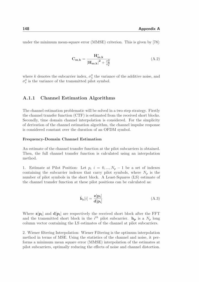
148 Appendix A
under the minimum mean-square error (MMSE) criterion. This is given by [78]:
Cm,k =H∗
m,k
|Hm,k|2 +σ2n
σ2s
(A.2)
where k denotes the subcarrier index, σ2n the variance of the additive noise, and
σ2s is the variance of the transmitted pilot symbol.
A.1.1 Channel Estimation Algorithms
The channel estimation problematic will be solved in a two step strategy. Firstlythe channel transfer function (CTF) is estimated from the received short blocks.Secondly, time domain channel interpolation is considered. For the simplicityof derivation of the channel estimation algorithm, the channel impulse responseis considered constant over the duration of an OFDM symbol.
Frequency-Domain Channel Estimation
An estimate of the channel transfer function at the pilot subcarriers is obtained.Then, the full channel transfer function is calculated using an interpolationmethod.
1. Estimate at Pilot Position: Let pi i = 0, ..., Np − 1 be a set of indexescontaining the subcarrier indexes that carry pilot symbols, where Np is thenumber of pilot symbols in the short block. A Least-Squares (LS) estimate ofthe channel transfer function at these pilot positions can be calculated as:
hp[i] =z[pi]
d[pi](A.3)
Where z[pi] and d[pi] are respectively the received short block after the FFTand the transmitted short block in the ith pilot subcarrier. hp is a Np longcolumn vector containing the LS estimates of the channel at pilot subcarriers.
2. Wiener filtering Interpolation: Wiener Filtering is the optimum interpolationmethod in terms of MSE. Using the statistics of the channel and noise, it per-forms a minimum mean square error (MMSE) interpolation of the estimates atpilot subcarriers, optimally reducing the effects of noise and channel distortion.

Descriptions 149
The full CTF is obtained by:
h = Rhhp·(Rhphp
+ σ2wINp
)−1hp (A.4)
where Rhhpis the cross correlation matrix of the true CTF and the true CTF at
pilot subcarriers, Rhphpis the autocorrelation matrix of the true CTF at pilot
subcarriers, σ2w is the noise power and INp
is the Np×Np identity matrix. Notethat the channel transfer function coefficients are assumed to be uncorrelatedto the noise process.
Time-Domain Channel Estimation
A simple time-domain channel estimation based on linear interpolation is as-sumed. In a sub-frame, the short block are transmitted. The channel estimationfor each sub-frame is a linear interpolation between these two short blocks.
A.1.2 Enhancement Mechanisms
Several throughput enhancement mechanisms are implemented in the simulator,including adaptive modulation coding (AMC) based on link adaptation (LA)and Hybrid ARQ (HARQ) based on fast L1 retransmissions. The HARQ isbased on chase combining (CC) and incremental redundancy (IR). LA withvarious modulations and channel coding sets (MCS) is applied to the shareddata channel. Here, a simple LA is assumed in which the MCS selection is basedon averaged SNR. No errors are assumed in the transmission of ACK/NACKmessages. As a result of the short retransmission delays, it is possible to operateat a 1st transmission block error rate (BLER) values of around 10-30%. Aretransmission scheme based on the stop and wait (SAW) principle with severalindependent HARQ processes per user is assumed [43].

150
A.2 Validation
This section provides the validation of the link level simulator. The validationstarts with the examining the performance of both QPSK and 16QAM in AWGNchannel. The results for uncoded BER of QPSK in AWGN channel is shownin Figure A.2. The simulated results is perfectly matched with the theoreticalcalculation as described in [79].
0 2 4 6 8 10 1210
−4
10−3
10−2
10−1
100
SNR (dB)
Unc
oded
BE
R
SimulatorTheoretical
Figure A.2: Uncoded BER results of QPSK in AWGN.
Figure A.3 shows the results for 16QAM and both simulated and theoreticalcalculation are obtained the same results.
Figure A.4 depicts the BLER performance in AWGN channel for several MCSsettings. The results are compared with the results presented in [2]. The turbodecoder used for both link-level simulations used a log-MAP decoding algorithm.Results show that the simulated results has a good agreement with the referenceresults. It is noted a small deviation of 0.3 dB for 16QAM rate 2/3.
Figure A.5 shows the BLER performance in typical urban channel. The result
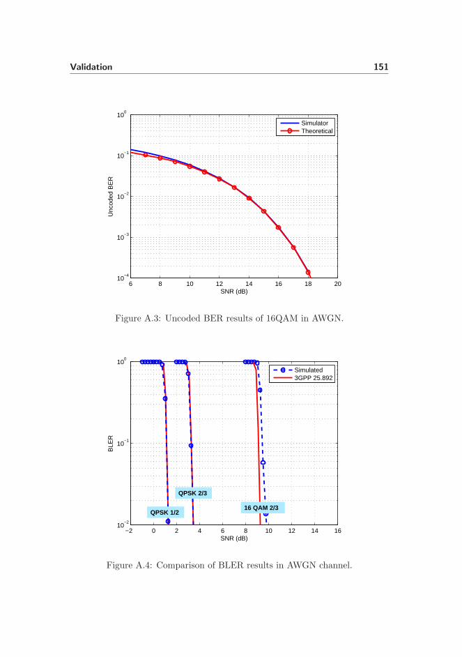
Validation 151
6 8 10 12 14 16 18 2010
−4
10−3
10−2
10−1
100
SNR (dB)
Unc
oded
BE
R
SimulatorTheoretical
Figure A.3: Uncoded BER results of 16QAM in AWGN.
−2 0 2 4 6 8 10 12 14 1610
−2
10−1
100
SNR (dB)
BLE
R
Simulated3GPP 25.892
16 QAM 2/3
QPSK 2/3
QPSK 1/2
Figure A.4: Comparison of BLER results in AWGN channel.
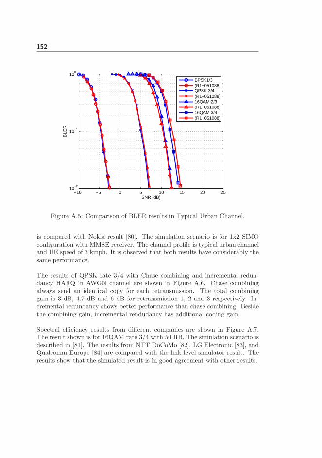
152
−10 −5 0 5 10 15 20 2510
−2
10−1
100
SNR (dB)
BLE
R
BPSK1/3(R1−051088)QPSK 3/4(R1−051088)16QAM 2/3(R1−051088)16QAM 3/4(R1−051088)
Figure A.5: Comparison of BLER results in Typical Urban Channel.
is compared with Nokia result [80]. The simulation scenario is for 1x2 SIMOconfiguration with MMSE receiver. The channel profile is typical urban channeland UE speed of 3 kmph. It is observed that both results have considerably thesame performance.
The results of QPSK rate 3/4 with Chase combining and incremental redun-dancy HARQ in AWGN channel are shown in Figure A.6. Chase combiningalways send an identical copy for each retransmission. The total combininggain is 3 dB, 4.7 dB and 6 dB for retransmission 1, 2 and 3 respectively. In-cremental redundancy shows better performance than chase combining. Besidethe combining gain, incremental rendudancy has additional coding gain.
Spectral efficiency results from different companies are shown in Figure A.7.The result shown is for 16QAM rate 3/4 with 50 RB. The simulation scenario isdescribed in [81]. The results from NTT DoCoMo [82], LG Electronic [83], andQualcomm Europe [84] are compared with the link level simulator result. Theresults show that the simulated result is in good agreement with other results.

Validation 153
−5 −4.5 −4 −3.5 −3 −2.5 −2 −1.5 −1 −0.5 0 0.5 1 1.5 2 2.5 3 3.5 4 4.5 5 5.5 60
0.2
0.4
0.6
0.8
1
1.2
1.4
SNR (dB)
Spe
ctra
l Effi
cien
cy (
b/s/
Hz)
QPSK 3/4 HARQ CCQPSK 3/4 HARQ CCQPSK 3/4 HARQ IRQPSK 3/4 HARQ IR
3 dB
1.7dB
1.3dB
Figure A.6: HARQ Chase Combining and Incremental Redundancy.
5 10 15 205
10
15
20
25
SNR (dB)
Thr
ough
put (
Mbp
s)
AAUQualcomm (R4−071200)LG (R4−071154)DoCoMo (R4−01364)
Figure A.7: Spectral Efficiency for 16QAM 3/4 in Typical Urban Channel.

154
Appendix B
Channel Model
The multipath channel model realization is based on the implementation in[85]. Several channel model have been implemented, including ITU Vehicular &Pedestrian channel, and Typical Urban channel. This channel model has alsobeen used in previous PhD project [86] in which the detailed channel modelverification is provided.
The channel model uses the correlation-based stochastic MIMO model. Toensure that the correlation properties in the frequency domain are realistic, thetypical urban with power delay profile (PDP) 6 paths and 20 paths are assumed.The path loss, shadowing, and other cell noise is modeled as AWGN noise. ThePDP of the typical urban is shown in Table B.1. These PDP have been used asthe tapped delay line coefficients to represent the multipath channel.
The frequency correlation property of both channels is shown in Figure B.1. Itis shown that the coherent bandwidth for both channels are equal at around 375kHz. Therefore, for a wideband transmission, i.e. 10 MHz, the channel profileis highly frequency selective fading channel.

156 Appendix B
Table B.1: Typical Urban Channel Power Delay Profile.
Number of TU 06 TU 20
path Delay (ns) Power (dB) Delay (ns) Power (dB)
1 0 -7.22 0 -5.7
2 195 -4.22 217 -7.6
3 488 -6.22 512 -10.1
4 1595 -10.22 514 -10.2
5 2311 -12.22 517 -10.2
6 5013 -14.22 674 -11.5
7 - - 882 -13.4
8 - - 1230 -16.3
9 - - 1287 -16.9
10 - - 1311 -17.1
11 - - 1349 -17.4
12 - - 1533 -19.0
13 - - 1535 -19.0
14 - - 1622 -19.8
15 - - 1818 -21.5
16 - - 1836 -21.6
17 - - 1884 -22.1
18 - - 1943 -22.6
19 - - 2048 -23.5
20 - - 2140 -24.3

Channel Model 157
0 0.5 1 1.5 2 2.5 3 3.5 4 4.5 50.4
0.5
0.6
0.7
0.8
0.9
1
Frequency (MHz)
Fre
quen
cy C
orre
latio
n
Typical Urban 20 pathsTypical Urban 6 paths
Figure B.1: Frequency correlation property of Typical Urban Channel Model.

158 Appendix B
Appendix C
Turbo Equalizer
C.1 System Model
The transmission scheme is presented in fig.C.1. A frame of information bitsbi is encoded by a turbo encoder. The resulting bl bits are interleaved usinga random permutation function. The interleaving coded bits bm are groupedin N q-length blocks {[b1,1, ..., b1,q] , ..., [bN,1, ..., bN,q]}, and each block of bits ismapped to a complex symbol si, i=1,...,M, where M = 2q is the number ofsymbols of the considered constellation. The SC-FDMA processing part of thetransmitter is identical to the OFDM one [5], except for the Discrete FourierTransform (DFT) spreading operation performed on the source symbol sequencesn, n=1,...,N before the subcarrier mapping operation
S[k] =1
N
N−1∑
n=0
snej2πkn
N k = 0, ...,N − 1 (C.1)
where N is the number of active subcarriers.
This operation spreads the source symbol sequence over all the subcarriers, so

160 Appendix C
Figure C.1: SC-FDMA transmitter
that each subcarrier takes information of the entire symbol sequence. Since thedata vector is processed by a DFT operation, the data generation is done intime-domain. The different samples are mapped to their definitive subcarrier(SMAP ) for the transmission [74].
Finally, the data is OFDM-processed by an IFFT block
x[p] =
NFFT−1∑
k=0
SMAP[k]e−j2πkl
N p = 0, ...,NFFT − 1 (C.2)
where NFFT is the FFT size, and a cyclic prefix (CP) is added [9], at the purposeof eliminating the intersymbol interference caused by time dispersive channel.SC-FDMA is expected to reduce the PAPR [87]; this characteristic is very im-portant for uplink since the UE has to be power-efficient due to battery limita-tions. Nevertheless, in SC-FDMA the symbol transmission is performed in timedomain; therefore it shows a noise enhancement compared with OFDM giventhat each received symbol contains the noise over all the frequencies.
In this work we assume that the maximum excess delay of the channel is shorterthan the ciclic prefix, and, therefore, the ISI can be completely removed.

System Model 161
Figure C.2: Turbo equalizer structure

162 Appendix C
C.2 Turbo Equalization
Considering that the frequency selective channel can be regarded as an encoderserially concatenated with the channel encoder of the transmitter, the mainidea of the turbo equalization is to perform jointly equalization/demodulationand decoding operation at the receiver [88]. In this case, equalizer and de-coder are considered as SISO (Soft Input Soft Output) blocks, separated bybit-deinterleavers and bit-interleavers: the information produced by one of theseblocks can be viewed as apriori information for the other one. The purpose ofthis system is to produce a more reliable estimation of the transmitted symbolsequence in each iteration. It is obtained through the progressive cancellationof the noise (interference) component and the knowledge of the structure of thecoded words given by the decoder.
The block diagram of our turbo equalizer is shown in Fig. C.2.
It uses soft interference cancellation (SIC) equalizer as described in [89] andthe equalization is performed in frequency domain. It results in more efficientoperation than traditional time domain equalization [90], since equalization isperformed on a block of data at a time, and the operations on this block involvean efficient FFT operation and a simple channel inversion operation.For the two receive antennas cases (1x2 SIMO), the received signals at eachantenna can be written as:
y1 = X · H1 + w1 (C.3)
y2 = X · H2 + w2 (C.4)
where X is diagonal matrix of the transmitted sub-carrier symbols, H1 and H2
are the channel frequency responses for the two antennas and w is the noisecomponent.
After the CP removal, the received signal is converted to frequency domainthrough a FFT operation. Frequency domain equalization is then performed,with a simple one tap equalizer. The equalizer coefficients are indicated as for-
ward coefficients (C(1)ff , C
(2)ff ), and these will be discussed in the next section.
After the maximal ratio combining (MRC) operation in SIMO case, the equal-ized signal is converted in time domain through an IDFT operation. The output

Turbo Equalization 163
is an estimation of the transmitted M-PSK or M-QAM symbols.
Remembering that at each symbol si of the constellation is associated a knownsequence of bits of length q, the log-likelihood ratio of all the coded bits iscomputed by using the max log MAP (Maximum A Posteriori) technique, asfollowing:
LE(bi,j) =(minǫi
k:bi,j=−1ǫik − minǫi
k:bi,j=1ǫik
)(C.5)
where bi,j is the jth bit associated at the constellation point si, k is the frequencybin, and ǫi
k denotes the squared euclidean distance of the equalizer output to si
, defined as:
ǫik =∣∣req,k − si
∣∣2 (C.6)
where req,k is the SIC equalizer output after the IFFT operation. The log-likelihood ratios of all the coded bits (LD
a (bl), obtained from (5) after theparallel-to-serial and the deinterleaving operations) are submitted to the turbodecoder, that should compute an improved log-likelihood ratio of all of them(LD(bl)), that takes into account of the knowledge of the encoder scheme. Thissoft output has been obtained modifying the structure of each MAP (Maxi-mum A Posteriori) decoder inside the turbo decoder structure [91], applyingthe BCJR algorithm [92] at both the systematic and the parity bits [93]. Atthis information is then subtracted the apriori information of the coded bits asfollows:
LDe (bl) = LD(bl) − LD
a (bl), (C.7)
at the purpose of extracting the so called extrinsic information [88] introducedby the channel encoder from LD(bl). Hence LD
e (bl) does not include any channelinformation.After the symmetrical interleaving operation, the resulting LE
a (·)s are groupedin q-length blocks
{[LE
e (b1,1), ..., LEa (b1,q)
], ...,
[LE
a (bN,1), ..., LEa (bN,q)
]}at the
purpose of constructing a matrix having in each row the log-likelihood ratiosof the bits related to each transmitted symbol. The probability of each bit iscomputed as follows:

164 Appendix C
Pe(bk,j = 0) =1
1 + exp(LEa (bk,j))
; (C.8)
Pe(bk,j = 1) = 1 − Pe(bk,j = 0). (C.9)
Thus, it is possible to compute the (NxM) apriori symbol probability matrix⌊Pa(si
k)⌋, that has in each row the probability of each symbol of the constellation
at frequency step k. Assuming independence between the interleaved coded bits,each element of this matrix is given by:
Pa(sik) =
q∏
j=1
Pe(bk,j = bi,j) (C.10)
for k=1,...N and i=1,...M.From each row of this matrix the estimation of the transmitted symbol vectorcan be computed:
sk = E(sik
)=
M∑
i=1
siPa(sik) (C.11)
So the estimated sequence is converted in frequency domain through a FFToperation, multiplied with the feedback coefficients (Cfb), in order to extractfrom it the noise component, and then subtracted from the equalized vector.Note that, for the next iterations of the algorithm, before passing the informa-tion generated by the equalizer to the decoder, the apriori information accruingfrom the previous iteration must be removed as follows:
Le(bl) = LD(bl) − La(bl) (C.12)
in order to prevent the decoder from ”reprocessing” its own information andhaving the so called ”positive feedback”[88].The computational complexity of the turbo equalizer processing is mostly re-lated to the computation of the (NxM) apriori symbol probability matrix, thatshould be recomputed at each iteration of the algorithm. Nevertheless, the com-plexity could be reduced through the Cyclic Redundancy Check (CRC) verifica-tion after the decoding operation: if the checking result is 0, no other iterationsare necessary.
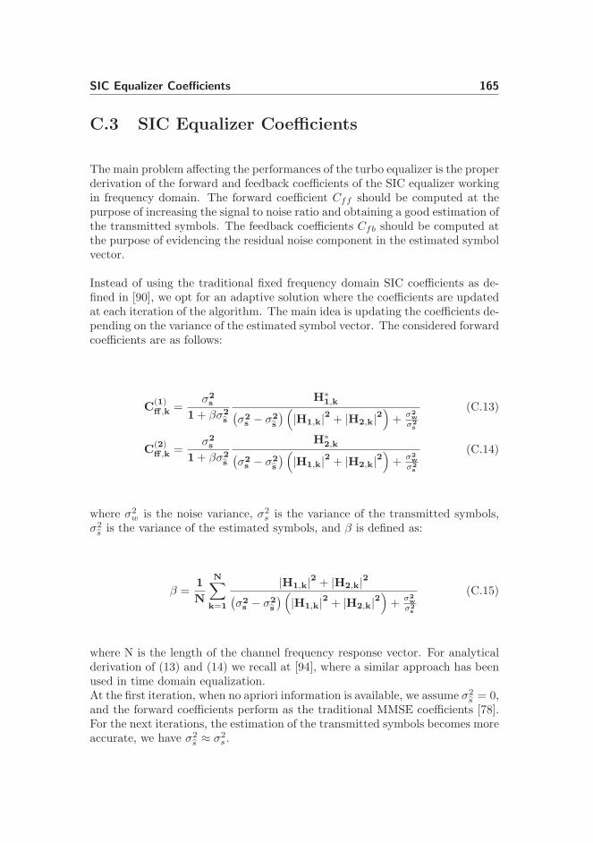
SIC Equalizer Coefficients 165
C.3 SIC Equalizer Coefficients
The main problem affecting the performances of the turbo equalizer is the properderivation of the forward and feedback coefficients of the SIC equalizer workingin frequency domain. The forward coefficient Cff should be computed at thepurpose of increasing the signal to noise ratio and obtaining a good estimation ofthe transmitted symbols. The feedback coefficients Cfb should be computed atthe purpose of evidencing the residual noise component in the estimated symbolvector.
Instead of using the traditional fixed frequency domain SIC coefficients as de-fined in [90], we opt for an adaptive solution where the coefficients are updatedat each iteration of the algorithm. The main idea is updating the coefficients de-pending on the variance of the estimated symbol vector. The considered forwardcoefficients are as follows:
C(1)ff ,k =
σ2s
1 + βσ2s
H∗
1,k(σ2s − σ2
s
) (|H1,k|2 + |H2,k|2
)+
σ2w
σ2s
(C.13)
C(2)ff ,k =
σ2s
1 + βσ2s
H∗
2,k(σ2s − σ2
s
) (|H1,k|2 + |H2,k|2
)+
σ2w
σ2s
(C.14)
where σ2w is the noise variance, σ2
s is the variance of the transmitted symbols,σ2
s is the variance of the estimated symbols, and β is defined as:
β =1
N
N∑
k=1
|H1,k|2 + |H2,k|2(σ2s − σ2
s
) (|H1,k|2 + |H2,k|2
)+
σ2w
σ2s
(C.15)
where N is the length of the channel frequency response vector. For analyticalderivation of (13) and (14) we recall at [94], where a similar approach has beenused in time domain equalization.At the first iteration, when no apriori information is available, we assume σ2
s = 0,and the forward coefficients perform as the traditional MMSE coefficients [78].For the next iterations, the estimation of the transmitted symbols becomes moreaccurate, we have σ2
s ≈ σ2s .
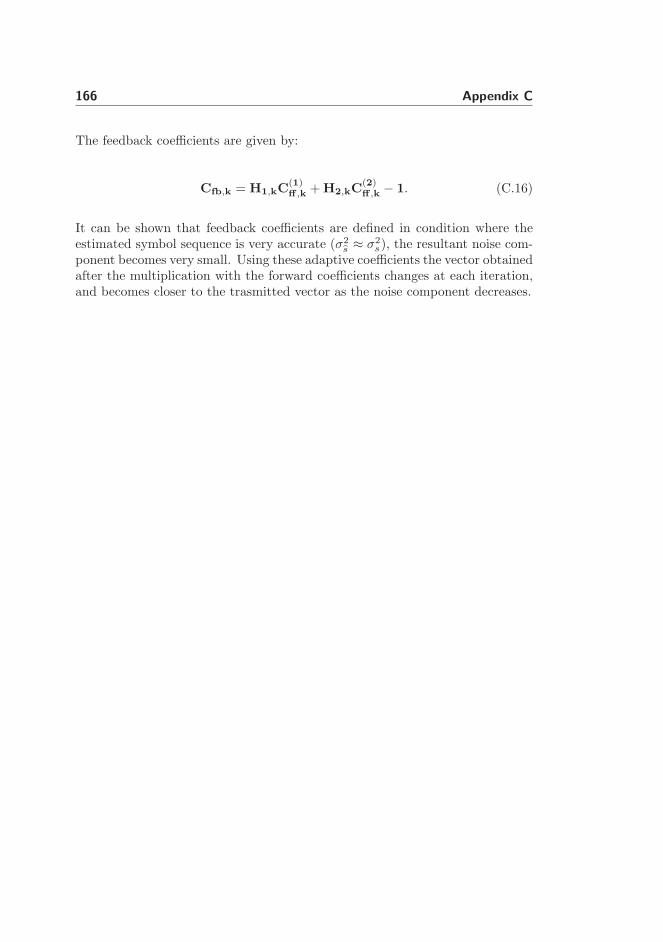
166 Appendix C
The feedback coefficients are given by:
Cfb,k = H1,kC(1)ff ,k + H2,kC
(2)ff ,k − 1. (C.16)
It can be shown that feedback coefficients are defined in condition where theestimated symbol sequence is very accurate (σ2
s ≈ σ2s), the resultant noise com-
ponent becomes very small. Using these adaptive coefficients the vector obtainedafter the multiplication with the forward coefficients changes at each iteration,and becomes closer to the trasmitted vector as the noise component decreases.

167

168
Bibliography
[1] P. Rysavy, “Mobile broadband: EDGE, HSPA, & LTE,” Online MaterialURL: http://www.itu.int/ITU-D/imt-2000/index.html, September 2006.
[2] 3GPP, “Feasibility study for orthogonal frequency division multiplexing(OFDM) for UTRAN enhancement,” Tech. Spec. TR 25.892 V6.0.0, June2004.
[3] J. Garcia, S. L. Jeunesse, and D. Bartow, “Measuring spurious free dynamicrange in a D/A converter,” Intersil, Tech. Rep. TB326, January 1995.
[4] J. Staudinger, “An overview of efficiency enhancements with applicationto linear handset power amplifier,” in Proc. IEEE Radio Freq. IntegratedCircuits Symposium., 2002.
[5] 3GPP, “Physical layer aspects for evolved universal terrestrial radio access(UTRA) (release 8),” Tech. Spec. TR 25.814 V7.1.0, September 2006.
[6] ——, “User Equipment (UE) radio transmission and reception (FDD) (re-lease 8),” TS 25.101 V8.1.0, December 2007.
[7] ——, “Requirements for Evolved UTRA (E-UTRA) and Evolved UTRAN(E-UTRAN),” TR 25.913, March 2006.
[8] 3GPP, “Physical channels & modulation,” TS 36.211 V0.2.2, December2006.
[9] D. Falconer, S. Ariyavisitakul, A. Benyamin-Seeyar, and B. Edison, “Fre-quency domain equalization for single-carrier broadband wireless systems,”IEEE Commun. Mag., vol. 40, no. 4, pp. 58–66, April 2002.

170 BIBLIOGRAPHY
[10] H. Sari, G. Karam, and I. Jeanclaude, “Transmission techniques for digitalterrestrial TV broadcasting,” IEEE Commun. Mag., vol. 33, no. 2, pp.100–109, February 1995.
[11] A. Czylwik, “Comparison between adaptive OFDM and single carrier mod-ulation with frequency domain equalization,” in Proc. Veh. TechnologyConf’97., vol. 2, Phoenix, AZ, May 1997, pp. 865–869.
[12] 3GPP, “Multiplexing and channel coding,” TS 25.212 V6.5.0(2005-06)),June 2005.
[13] E. Costa and S. Pupolin, “M-QAM-OFDM system performance in the pres-ence of a nonlinear amplifier and phase noise,” IEEE Trans. on Communi-cations, vol. 50, no. 3, pp. 462–472, March 2002.
[14] A. Georgiadis, “Gain, Phase Imbalance, and Phase Noise Effects on ErrorVector Magnitude,” IEEE Trans. on Vehicular Technology, vol. 53, no. 2,March 2004.
[15] Q. Gu, RF System Design of Transceivers for Wireless Communications.New York, USA: Springer, 2006.
[16] B. Razavi, RF Microelectronics, 1st ed. New Jersey, USA: Prentice HallPTR, 1998.
[17] B. Priyanto, T. Sørensen, and O. Jensen, “On investigation of nonlinearamplifier distortion in OFDM transmission,” in Proc. Wireless PersonalMultimedia Communications 2005., September 2005.
[18] S. Han and J. Lee, “An overview of peak-to-average power ratio reductiontechniques for multicarrier transmission,” IEEE Wireless Communications,vol. 12, no. 2, pp. 56–65, April 2005.
[19] B. Priyanto, C. Rom, C. Navarro, T. Sørensen, , P. Mogensen, andO. Jensen, “Effect of phase noise on spectral efficiency for UTRA LongTerm Evolution,” in Proc. IEEE PIMRC 2006., September 2006.
[20] A. Diet, C. Berland, M. Villegas, and G. Baudoin, “EER architecture speci-fications for OFDM transmitter using a class E amplifier,” IEEE Microwaveand Wireless Comp. Letters, vol. 14, no. 8, August 2004.
[21] M. Talonen and S. Lindfors, “System requirements for OFDM polar trans-mitter,” in Proc. Euro Conf. on Circuit Theory and Design, vol. 3, August2005.
[22] Y. Huang and T. Larsen, “Investigation of polar transmitter for WCDMAhandset applications,” in Proc. IEEE NORCHIP 2006., November 2006.

BIBLIOGRAPHY 171
[23] F. Raab, “Power amplifiers and transmitters for RF and microwave,” IEEETrans.on Microwave Theory and Tech., vol. 50, no. 3, March 2002.
[24] D. Rudolph, “Out-of-band emissions of digital transmissions using kahnEER technique,” IEEE Trans.on Microwave Theory and Tech., vol. 50,no. 8, August 2002.
[25] M. Faulkner, “The effect of filtering on the performance of OFDM systems,”IEEE Trans. On Veh. Tech, vol. 49, no. 5, September 2000.
[26] B. Razavi, “RF transmitter architectures and circuits,” in Proc. IEEE Cus-tom Integrated Circuits., vol. 12, San Diego, CA, May 1999, pp. 197–204.
[27] M. Feulner, “Direct up-conversion lowers base-station costs,” Wireless Eu-rope Mag., vol. 38, pp. 27–28, April 2005.
[28] A. Loke and F. Ali, “Direct conversion radio for digital mobile phone-design issues, status, and trends,” IEEE Trans. Microwave Theory andTechniques, vol. 50, no. 11, pp. 2422–2435, November 2002.
[29] J. MacLeod, M. Beach, P. Warr, and T. Nesimoglu, “Filter considerations inthe design of a software-defined radio,” in Proc. IST Mobile CommunicationSummit., vol. 1, Barcelona, Spain, September 2001, pp. 363–368.
[30] S. C. Cripps, RF Power Amplifiers for Wireless Communications, 2nd ed.Norwood, MA: Artech House, 2006.
[31] S. Mann, M. Beach, and J. McGeehan, “Increasing the talk-time of mobileradios with efficient linear transmitter architectures,” Elec and CommunEngineering Journal, vol. 13, no. 2, pp. 65–76, April 2001.
[32] X. Huang, “On transmitter gain/phase imbalance compensation at re-ceiver,” IEEE Communications on Letters, vol. 4, no. 11, November 2000.
[33] W. Songping and Y. Bar-Ness, “OFDM systems in the presence of phasenoise: Consequences and solutions,” IEEE Trans. Communications, vol. 52,no. 5, pp. 855–865, May 2004.
[34] A. Armada, “Understanding the effects of phase noise in orthogonal fre-quency division multiplexing (OFDM),” IEEE Trans. Broadcasting, vol. 47,no. 2, pp. 153–159, June 2001.
[35] Ericsson, “Impact of EVM on data throughput for different transmitterimpairments,” 3GPP, Gyeongju, Korea, Tech. Rep. R4-020779, May 2002.
[36] C. Masse, “A direct-conversion transmitter for WIMAX and WiBro appli-cations,” RF design Mag., vol. 1, pp. 42–46, January 2006.
172 BIBLIOGRAPHY
[37] L. Kahn, “Single-sideband transmission by envelope elimination andrestoration,” Proc. of IRE, pp. 803–806, July 1952.
[38] Y. Huang, Y. Wang, and T. Larsen, “Filter considerations in polar trans-mitters for multi-mode wireless applications,” in Proc. IEEE Wireless Mi-crowave Tech. 2005., November 2005, pp. 133–136.
[39] F. Wang, D. F. Kimball, J. D. Popp, A. H. Yang, D. Y. Lie, P. M. Asbeck,and L. E. Larson, “An improved power-added efficiency 19-dBm hybridenvelope elimination and restoration power amplifier for 802.11g WLANapplications,” IEEE Trans. Microwave Theory and Techniques, vol. 52,no. 12, pp. 4086–4099, December 2006.
[40] J. Bingham, “Multicarrier modulation for data transmission: An ideawhoce time has come,” IEEE Commun Mag., pp. 5–14, May 1990.
[41] K. Kansanen, “Wireless broadband single-carrier systems with MMSETurbo Equalization Receivers,” Ph.D. dissertation, University of Oulu,Oulu, Finland, 2005.
[42] L. Electronics, “PAPR comparison of uplink MA schemes,” 3GPP, Athens,Greece, Tech. Rep. R1-050475, May 2005.
[43] T. Kolding, F. Frederiksen, and P. Mogensen, “Performance aspects ofWCDMA systems with High Speed Downlink Packet Access (HSDPA),” inProc. IEEE VTC Fall 2002., Vancouver, Canada, July 2002, pp. 477–481.
[44] H. Holma and A. Toskala, WCDMA for UMTS, HSPA evolution and LTE,4th ed. Chichester, UK: Wiley, 2007.
[45] P. Hoher, “TCM on frequency-selective land-mobile fading channels,” inProc. Intl. Workshop on Digital Communications., vol. 1, Tirrena, Italy,September 1991.
[46] 3GPP, “Deployment aspects,” TR 25.943 V7.0.0, June 2006.
[47] Ericsson, “Impact of EVM on data throughput for different transmitterimpairments,” 3GPP, Tech. Rep. R4-020779, May 2002.
[48] Motorola, “Effect of modulation accuracy on HSDPA radio link perfor-mance,” 3GPP, Tech. Rep. R4-011439, November 2001.
[49] Nokia, “Definition of E-UTRA EVM for the BS,” 3GPP, Tallinn, Estonia,Tech. Rep. R4-060737, September 2006.
[50] ——, “Methodology for deriving E-UTRA EVM BS requirements,” 3GPP,Tallinn, Estonia, Tech. Rep. R4-060738, September 2006.

BIBLIOGRAPHY 173
[51] Siemens, “EVM Measure for LTE,” 3GPP, Riga, Latvia, Tech. Rep. R4-061227, November 2006.
[52] 3GPP, “Base station (BS) conformance testing (FDD),” Tech. Spec. TS25.141 V7.6.0, December 2006.
[53] T. Larsen, O. Jensen, and J. Mikkelsen, “Power amplifier modeling forvarying envelope modulation,” in Proc. IEEE NORCHIP Conf., November2004.
[54] A. Koukab, Y. Lei, and M. Declercq, “Multi-standard carrier generationsystem for quad-band GSM/WCDMA (FDD-TDD)/WLAN (802.11 a-b-g)radio,” in Proc. IEEE ESSCIRC., 2005.
[55] Motorola, “64 QAM for UL LTE,” 3GPP, St.Louis, Missouri, USA, Tech.Rep. R1-070759, February 2007.
[56] 3GPP, “Evolved UTRA (E-UTRA) user equipment (UE) radio transmis-sion and reception,” TR 36.803 V1.0.0, December 2007.
[57] Nokia, “Analysis of LTE UL spectrum shaping requirements,” 3GPP, Riga,Latvia, Tech. Rep. R4-061314, November 2006.
[58] Huawei, “Analysis of out-of-band spectrum emission of uplink transmissionunder current numerology,” 3GPP, Cannes, France, Tech. Rep. R1-061857,June 2006.
[59] Freescale, “Spectral mask issues for the LTE Uplink,” 3GPP, Tallin, Esto-nia, Tech. Rep. R4-061004, August 2006.
[60] Ericsson, “UE ACLR and spectrum emission requirements,” 3GPP, SophiaAntipolis, France, Tech. Rep. R4-070388, April 2007.
[61] N. S. Networks, Nokia, V. Wireless, Vodafone, and Ericsson, “Recom-mendations on lower E-UTRA bandwidth options,” 3GPP, Orlando, USA,Tech. Rep. R4-070918, June 2007.
[62] Nokia, “Considerations regarding specification of E-UTRA BS spectrumshaping,” 3GPP, Tallin, Estonia, Tech. Rep. R4-060746, August 2006.
[63] L. Technologies, “Windowing and spectral containment for OFDM down-link,” 3GPP, London, UK, Tech. Rep. R1-050919, August 2005.
[64] Nokia, “UE ACLR and SEM,” 3GPP, Sophia Antipolis, France, Tech. Rep.R4-070348, April 2007.
[65] M. Elliott, T. Montalvo, B. Jeffries, F. Murden, J. Strange, A. Hill,S. Nandipaku, and J. Harrebek, “A polar modulator transmitter forGSM/EDGE,” IEEE Trans. on Solid-State Circuits, vol. 39, no. 12, pp.2190–2199, December 2004.

174 BIBLIOGRAPHY
[66] N. D. Lopez, J. Xufeng, D. Maksimovic, and Z. Popovic, “Class-E poweramplifier in a polar EDGE transmitter,” in Int. IEEE Microwave Sympo-sium Digest, vol. 1, June 2006, pp. 785–788.
[67] J. Staudinger, B. Gilsdorf, D. Newman, G. Norris, G. Sadowniczak, R. Sher-man, and T. Quach, “High efficiency CDMA RF power amplifier using dy-namic envelope tracking technique,” in Int. IEEE Microwave SymposiumDigest., vol. 2, June 2000, pp. 873–876.
[68] 3GPP, “User Equipment (UE) radio transmission and reception (FDD)(release 7),” TS 25.101 V7.7.0, March 2007.
[69] B. Priyanto, T. Sørensen, O. Jensen, T. Kolding, T. Larsen, and P. Mo-gensen, “A spectrum shaping technique to control spectrum emission ofUTRA LTE User Equipment,” in Proc. IEEE NORCHIP 2007., November2007.
[70] W. Zhengdao, M. Xiaoli, and G. Giannakis, “OFDM or single-carrier blocktransmissions?” IEEE Trans. Communications, vol. 52, no. 3, pp. 380–394,March 2004.
[71] N. S. Networks, “On in-band adjacent RB selectivity requirements,” 3GPP,Athens, Greece, Tech. Rep. R4-071402, August 2006.
[72] Ericsson, “Initiation of modulation quality discussions for LTE,” 3GPP,Denver, USA, Tech. Rep. R4-060071, February 2006.
[73] ——, “On UE in-band unwanted emissions,” 3GPP, Tallinn, Estonia, Tech.Rep. R4-060881, September 2006.
[74] B. Priyanto, H. Codina, S. Rene, T. Sørensen, and P. Mogensen, “Ini-tial Performance Evaluation of DFT-Spread OFDM based SC-FDMA forUTRA LTE Uplink,” in Proc. IEEE VTC Spring 2007., April 2007.
[75] CATT, Ericsson, LGE, Motorola, Nokia, Nokia-Siemens, Nortel, N. Do-CoMo, Orange, Panasonic, Philips, Qualcomm, S. Samsung, TI, and Voda-fone, “Way forward on power control of pusch,” 3GPP, Orlando, USA,Tech. Rep. R1-073224, June 2007.
[76] Nokia, “LTE UL coexistence with LTE and other radio technologies,”3GPP, Tallinn, Estonia, Tech. Rep. R4-060764, September 2006.
[77] K. Fazel and S. Kaiser, Multi-Carrier and Spread Spectrum Systems.Chichester, UK: Wiley, 2003.
[78] H. Sari, G. Karam, , and I. Jeanclaude, “Frequency-domain equalizationof mobile radio and terrestrial broadcast channels,” in Proc. IEEE GlobalTelecommun. Conf., vol. 1, November 1994.

BIBLIOGRAPHY 175
[79] J. G. Proakis, Digital Communications, 4th ed. New York, USA: McGraw-Hill, 2001.
[80] Nokia, “Coverage comparison between UL OFDMA and SC-FDMA,”3GPP, San Diego, USA, Tech. Rep. R1-051088, October 2005.
[81] Ericsson, “Common simulation assumptions for eNodeB demodulation re-quirements,” 3GPP, Orlando, US, Tech. Rep. R4-070983, June 2007.
[82] N. DoCoMo, “Initial simulation results for LTE UL Demodulation,” 3GPP,Athens, Greece, Tech. Rep. R4-071364, August 2007.
[83] L. Electronics, “Simulation results for LTE eNodeB demodulation perfor-mance with rel-6 Turbo codec,” 3GPP, Athens, Greece, Tech. Rep. R4-071154, August 2007.
[84] Q. Europe, “LTE eNB demodulation link performance,” 3GPP, Athens,Greece, Tech. Rep. R4-0701200, August 2007.
[85] L. Schumacher, J. Kermoal, F. Frederiksen, K. Pedersen, A. Algans, andP. Mogensen, “MIMO Channel Characterisation,” IST Project, Tech. Rep.IST-1999-11729, February 2001, METRA Deliverable.
[86] L. Berger, “Performance of Multi-Antenna Enhanced HSDPA,” Ph.D. dis-sertation, Aalborg University, Aalborg, Denmark, 2005.
[87] J. Tubbax, B. Come, L. Perre, L. Deneire, and M. Engels, “OFDM versussingle carrier with cyclic prefix: A system-based comparison,” in Proc. 54thVeh. Technology Conf’2001., vol. 2, Atlantic City, NJ, October 2001, pp.1115–1119.
[88] R. Koetter, A. Singer, and M. Tuchler, “Turbo equalization,” IEEE SignalProcessing Mag., vol. 21, no. 1, pp. 67–80, January 2004.
[89] C. Laot, A. Glavieux, and J. Labat, “Turbo equalization: adaptive equal-ization and channel decoding jointly optimized,” IEEE Journal on Sel.Areas in Commun., vol. 19, no. 9, pp. 1744–1752, September 2001.
[90] M. Tuchler and J. Hagenauer, “Turbo equalization using frequency domainequalizers,” in Proc. Allerton Conference., vol. 1, Monticello, AR, October2000, pp. 144–153.
[91] W. Ryan, “A turbo code tutorial,” Online Material URL:http://www.ece.arizona.edu/ ryan/publications/turbo2c.pdf, pp. 1–9,1997.
[92] C. Berrou, A. Glavieux, and P. Thitimajshima, “Near shannon limit error-correcting coding and decoding: Turbo codes,” in Proc. 1993 Int.Conf.Comm., Geneva, Switzerland, May 1993, pp. 1064–1070.

176 BIBLIOGRAPHY
[93] D. Raphaeli and Y. Zarai, “Combined turbo equalization and turbo de-coding,” IEEE Communications Letters, vol. 2, no. 4, pp. 107–109, April1998.
[94] C. Laot and R. Bidan, “Low-complexity MMSE turbo equalization: Apossible solution for EDGE,” IEEE Transactions on Wireless Communica-tions, vol. 4, no. 3, pp. 965–974, May 2005.