al39 - multics processor manualthis manual includes the processor capabilities, modes of operation,...
TRANSCRIPT

HONEYWELL
DPS/LEVEL 68 &DPS 8MMULTICSPROCESSORMANUAL
HARDWARE

PREFACE
This manual describes the processors used in the Multics system. These are the DPS/L68, which refers to the DPS, L68 or older model processors (excluding the GE-645) and DPS 8M, which refers to the DPS 8 family of Multics processors, i.e. DPS 8/70M, DPS 8/62M and DPS 8/52M. The reader should be familiar with the overall modular organization of the Multics system and with the philosophy of asynchronous operation. In addition, this manual presents a discussion of virtual memory addressing concepts including segmentation and paging.
The manual is intended for use by systems programmers responsible for writing software to interface with the virtual memory hardware and with the fault and interrupt portions of the hardware. It should also prove valuable to programmers who must use machine instructions (particularly language translator implementors) and to those persons responsible for analyzing crash conditions in system dumps.
This manual includes the processor capabilities, modes of operation, functions, and detailed descriptions of machine instructions. Data representation, program-addressable registers, addressing by means of segmentation and paging, faults and interrupts, hardware ring implementation, and cache operation are also covered.
The information and specifications in this document are subject to change without notice. Consult your Honeywell Marketing Representative for product or service availability.
11/85©Honeywell Information Systems Inc., 1985 File No.: 1L03, 1L53 AL39-01C

CONTENTS
Preface...............................................................................................................................................2
Section 1: Introduction.......................................................................................................................8Multics Processor Features.......................................................................................8
Segmentation and Paging...................................................................................8Address Modification and Address Appending...................................................9Faults and Interrupts..........................................................................................9
Processor Modes of Operation..................................................................................9Instruction Execution Modes............................................................................10
Normal Mode.............................................................................................10Privileged Mode.........................................................................................10
Addressing Modes............................................................................................10Absolute Mode...........................................................................................10Append Mode.............................................................................................10BAR Mode..................................................................................................10
Processor Unit Functions........................................................................................10Appending Unit.................................................................................................11Associative Memory Assembly..........................................................................11Control Unit......................................................................................................11Operation Unit..................................................................................................11Decimal Unit.....................................................................................................11
Section 2: Data Representation........................................................................................................12Information Organization........................................................................................12Position Numbering.................................................................................................12Number System.......................................................................................................12Information Formats...............................................................................................13Data Parity..............................................................................................................14Representation of Data............................................................................................14
Numeric Data...................................................................................................15Fixed-point Binary Data.............................................................................15Floating-point Binary Data.........................................................................17Decimal Data.............................................................................................19
Alphanumeric Data...........................................................................................21Character String Data................................................................................22Bit String Data...........................................................................................22
Section 3: Program Accessible Registers.........................................................................................23Accumulator Register (A)........................................................................................24Quotient Register (Q)..............................................................................................24Accumulator-Quotient Register (AQ).......................................................................25Exponent Register (E).............................................................................................25Exponent-Accumulator-Quotient Register (EAQ).....................................................26Index Registers (Xn)................................................................................................26Indicator Register (IR).............................................................................................27Base Address Register (BAR)..................................................................................30Timer Register (TR).................................................................................................30Ring Alarm Register (RALR)....................................................................................31Pointer Registers (PRn)...........................................................................................31Address Registers (ARn)..........................................................................................32Procedure Pointer Register (PPR)...........................................................................33Temporary Pointer Register (TPR)..........................................................................34Descriptor Segment Base Register (DSBR).............................................................36Segment Descriptor Word Associative Memory (SDWAM)......................................37Page Table Word Associative Memory (PTWAM)....................................................39Fault Register (FR) – DPS and L68..........................................................................41Fault Register (FR) - DPS 8M..................................................................................43Mode Register (MR) - DPS and L68.........................................................................45

Mode Register (MR) - DPS 8M................................................................................48Cache Mode Register (CMR) - DPS and L68...........................................................49Cache Mode Register (CMR) - DPS 8M...................................................................51Control Unit (CU) History Registers - DPS and L68................................................53Control Unit (CU) History Registers - DPS 8M........................................................55Operations Unit (OU) History Registers - DPS and L68..........................................57Decimal Unit (DU) History Registers - DPS and L68...............................................59Decimal/Operations Unit (DU/OU) History Registers - DPS 8M..............................61Appending Unit (APU) History Registers - DPS and L68.........................................64Appending Unit (APU) History Registers – DPS 8M................................................65Configuration Switch Data - DPS and L68...............................................................68Configuration Switch Data - DPS 8M......................................................................69Control Unit Data....................................................................................................71Decimal Unit Data...................................................................................................76
Section 4: Machine Instructions.......................................................................................................79Instruction Repertoire.............................................................................................79
Arrangement of Instructions.............................................................................79Basic Operations...............................................................................................79Extended Instruction Set (EIS) Operations.......................................................79
EIS Single-Word Operations......................................................................79EIS Multiword Operations.........................................................................80
Format of Instruction Description...........................................................................80Definitions of Notation and Symbols.......................................................................82
Main Memory Addresses..................................................................................82Index Values.....................................................................................................82Abbreviations and Symbols...............................................................................82Register Positions and Contents.......................................................................83Other Symbols..................................................................................................84
Common Attributes of Instructions.........................................................................84Illegal Modification...........................................................................................84Parity Indicator.................................................................................................84
Instruction Word Formats.......................................................................................85Basic and EIS Single-Word Instructions...........................................................85Indirect Words..................................................................................................85EIS Multiword Instructions..............................................................................86EIS Modification Fields (MF)............................................................................87
MF Coding Examples.................................................................................89EIS Operand Descriptors and Indirect Pointers...............................................89
Operand Descriptor Indirect Pointer Format.............................................89Alphanumeric Operand Descriptor Format................................................90Numeric Operand Descriptor Format........................................................91Bit-string Operand Descriptor Format.......................................................93
Fixed-point Arithmetic Instructions.........................................................................94Fixed-Point Data Movement Load.....................................................................94Fixed-Point Data Movement Store..................................................................100Fixed-Point Data Movement Shift...................................................................107Fixed-Point Addition.......................................................................................111Fixed-Point Subtraction..................................................................................117Fixed-Point Multiplication..............................................................................122Fixed-Point Division........................................................................................124Fixed-Point Negate.........................................................................................126Fixed-Point Comparison.................................................................................127Fixed-Point Miscellaneous..............................................................................131
Boolean Operation Instructions.............................................................................132Boolean And....................................................................................................132Boolean Or......................................................................................................134Boolean Exclusive Or......................................................................................136Boolean Comparative And..............................................................................138Boolean Comparative Not...............................................................................140
Floating-point Arithmetic Instructions..................................................................142
Floating-Point Data Movement Load..............................................................142Floating-Point Data Movement Store..............................................................143Floating-Point Addition...................................................................................145Floating-Point Subtraction..............................................................................147Floating-Point Multiplication..........................................................................149Floating-Point Division...................................................................................151Floating-Point Negate.....................................................................................154Floating-Point Normalize................................................................................155Floating-Point Round......................................................................................156Floating-Point Compare..................................................................................158Floating-Point Miscellaneous..........................................................................160
Transfer Instructions.............................................................................................162Pointer Register Instructions................................................................................171
Pointer Register Data Movement Load...........................................................171Pointer Register Data Movement Store..........................................................175Pointer Register Address Arithmetic..............................................................178Pointer Register Miscellaneous......................................................................179
Miscellaneous Instructions....................................................................................180Calendar Clock...............................................................................................180Derail..............................................................................................................181Execute...........................................................................................................182Master Mode Entry.........................................................................................184No Operation..................................................................................................186Repeat............................................................................................................187Ring Alarm Register.......................................................................................193Store Base Address Register..........................................................................194Translation......................................................................................................195
Register Load........................................................................................................197Privileged Instructions..........................................................................................198
Privileged - Register Load..............................................................................198Privileged - Register Store..............................................................................203Privileged - Clear Associative Memory...........................................................209Privileged - Configuration and Status.............................................................212Privileged – System Control............................................................................215Privileged - Miscellaneous..............................................................................218
Extended Instruction Set (EIS)..............................................................................219EIS - Address Register Load...........................................................................219EIS - Address Register Store..........................................................................222EIS - Address Register Special Arithmetic.....................................................225EIS - Alphanumeric Compare.........................................................................233EIS - Alphanumeric Move...............................................................................243EIS - Numeric Compare..................................................................................249EIS - Numeric Move.......................................................................................251EIS - Bit String Combine................................................................................255EIS - Bit String Compare................................................................................258EIS - Bit String Set Indicators........................................................................260EIS - Data Conversion.....................................................................................262EIS - Decimal Addition....................................................................................265EIS - Decimal Subtraction..............................................................................270EIS - Decimal Multiplication...........................................................................272EIS - Decimal Division....................................................................................275
Micro Operations for Edit Instructions..................................................................278Micro Operation Sequence.............................................................................278Edit Insertion Table........................................................................................278Edit Flags.......................................................................................................279Terminating Micro Operations.......................................................................279MVNE and MVE Differences..........................................................................279
Numeric Edit............................................................................................279Alphanumeric Edit...................................................................................280
Micro Operations............................................................................................280Micro Operation Code Assignment Map.........................................................287

Section 5: Addressing -- Segmentation and Paging........................................................................288Addressing Modes.................................................................................................288
Absolute Mode................................................................................................288Append Mode..................................................................................................288
Segmentation........................................................................................................288Paging...................................................................................................................289Changing Addressing Modes.................................................................................292Address Appending................................................................................................292
Address Appending Sequences.......................................................................292Appending Unit Data Word Formats.....................................................................294
Segment Descriptor Word (SDW) Format......................................................294Page Table Word (PTW) Format.....................................................................296
Section 6: Virtual Address Formation............................................................................................297Definition of Virtual Address.................................................................................297Types of Virtual Address Formation......................................................................297Symbology (ALM)..................................................................................................298
Symbolic Fields..............................................................................................298ALM Pseudo-Instructions................................................................................298
Computed Address Formation...............................................................................299The Address Modifier (TAG) Field..................................................................299General Types of Computed Address Modification.........................................299Computed Address Formation Flowcharts.....................................................300Register (r) Modification................................................................................300Register Then Indirect (ri) Modifications.......................................................302Indirect Then Register (ir) Modification.........................................................303Indirect Then Tally (it) Modification...............................................................305
Virtual Address Formation Involving Both Segment Number and Computed Address..................................................................................................................311
The Use of Bit 29 in the Instruction Word......................................................311Special Address Modifiers..............................................................................312
Indirect to Pointer (ITP) Modification......................................................312Indirect to Segment (ITS) Modification....................................................313
Effective Segment Number Generation..........................................................314Virtual Address Formation for Extended Instruction Set......................................316
Character- and Bit-String Addressing.............................................................317Character- and Bit-String Address Arithmetic Algorithms..............................318
9-bit Byte String Address Arithmetic.......................................................3186-bit Character String Address Arithmetic..............................................3184-bit Byte String Address Arithmetic.......................................................319Bit String Address Arithmetic..................................................................319
Section 7: Faults and Interrupts ....................................................................................................320Fault Cycle Sequence............................................................................................320Fault Priority.........................................................................................................322Fault Recognition..................................................................................................322Fault Descriptions.................................................................................................323
Group 1 Faults................................................................................................323Group 2 Faults................................................................................................323Group 3 Faults................................................................................................324Group 4 Faults................................................................................................324Group 5 Faults................................................................................................325Group 6 Faults................................................................................................325Group 7 Faults................................................................................................326
Interrupts and External Faults..............................................................................326Interrupt Sampling.........................................................................................327Interrupt Cycle Sequence...............................................................................327
Section 8: Hardware Ring Implementation....................................................................................329Ring Protection in Multics.....................................................................................329Ring Protection in the Processor...........................................................................330

Appending Unit Operation with Ring Mechanism.................................................330
Section 9: DPS/L68 Cache Memory Operation...............................................................................342Philosophy of Cache Memory................................................................................342Cache Memory Organization.................................................................................342
Cache Memory / Main Memory Mapping........................................................342Cache Memory Addressing.............................................................................343
Cache Memory Control..........................................................................................345Enabling and Disabling Cache Memory..........................................................345Cache Memory Control in Segment Descriptor Words...................................345Loading the Cache Memory............................................................................346Clearing the Cache Memory...........................................................................346
General Clear...........................................................................................346Selective Clear.........................................................................................346
Dumping the Cache Memory..........................................................................347
Appendix A: Operation Code Map..................................................................................................348
Appendix B: Alphabetic Operation Code List.................................................................................351EIS Micro Operations.....................................................................................357
Appendix C: Address Modifiers......................................................................................................358Nonstandard Modifiers..........................................................................................358

SECTION 1: INTRODUCTION
The processor described in this reference manual is a hardware module designed for use with Multics. The many distinctive features and functions of Multics are enhanced by the powerful hardware features of the processor. The addressing features, in particular, are designed to permit the Multics software to compute relative and absolute addresses, locate data and programs in the Multics virtual memory, and retrieve such data and programs as necessary.
MULTICS PROCESSOR FEATURES
The Multics processor contains the following general features:
1. Storage protection to place access restrictions on specified segments.
2. Capability to interrupt program execution in response to an external signal (e.g., I/O termination) at the end of any even/odd instruction pair (midinstruction interrupts are permitted for some instructions), to save processor status, and to restore the status at a later time without loss of continuity of the program.
3. Capability to fetch instruction pairs and to buffer two instructions (up to four instructions, depending on certain main memory overlap conditions) including the one currently in execution.
4. Overlapping instruction execution, address preparation, and instruction fetch. While an instruction is being executed, address preparation for the next operand (or even the operand following it) or the next instruction pair is taking place. The operations unit can be executing instruction N, instruction N+1 can be buffered in the operations unit (with its operand buffered in a main memory port), and the control unit can be executing instructions N+2 or N+3 (if such execution does not involve the main memory port or registers of instructions N or N+1) or preparing the address to fetch instructions N+4 and N+5. This includes the capability to detect store instructions that alter the contents of buffered instructions and the ability to delay preprocessing of an address using register modification if the instruction currently in execution changes the register to be used in that modification.
5. Interlacing capability to direct main memory accesses to interlaced system controller modules.
6. Intermediate storage of address and control information in high-speed registers addressable by content (associative memory).
7. Intermediate storage of base address and control information in pointer registers that are loaded by the executing program.
8. Absolute address computation at execution time.
9. Ability to hold recently referenced operands and instructions in a high-speed look-aside memory (cache option).
Segmentation and Paging
A segment is a collection of data or instructions that is assigned a symbolic name and addressed symbolically by the user. Paging is controlled by the system software; the user need not be aware of the existence of pages. User-visible address preparation is concerned with the calculation of a virtual memory address; the processor hardware completes address preparation by translating the final virtual memory address into an absolute main memory address. The user may view each of his segments as residing in an independent main memory unit. Each segment has its

own origin that can be addressed as location zero. The size of each segment varies without affecting the addressing of the other segments. Each segment can be addressed like a conventional main memory image starting at location zero. Maximum segment size is 262,144 words.
When viewed from the processor, main memory consists of blocks or page frames, each of which has a length of "page-size" words. The page size used by Multics is 1024 words. Each frame begins at an absolute address which is zero modulo the page size. Any page of a segment can be placed in any available main memory frame. These pages may be addressed as if they were contiguous, even though they may be in widely scattered absolute locations. Only currently referenced pages need be in main memory. A segment need not be paged, in which case the complete segment is located in contiguous words of main memory. In Multics, all user segments are paged. See Section 5 for additional discussion.
Address Modification and Address Appending
Before each main memory access, two major phases of address preparation take place:
1. Address modification by register or indirect word content, if specified by the instruction word or indirect word.
2. Address appending, in which a virtual memory address is translated into an absolute address to access main memory.
Although the above two types of modification are combined in most operations, they are described separately in Sections 5 and 6. The address modification procedure can go on indefinitely, with one type of modification leading to repetitions of the same type or to other types of modification prior to a main memory access for an operand.
Faults and Interrupts
The processor detects certain illegal instruction usages, faulty communication with the main memory, programmed faults, certain external events, and arithmetic faults. Many of the processor fault conditions are deliberately or inadvertently caused by the software and do not necessarily involve error conditions. The processor communicates with the other system modules (I/O multiplexers, bulk store controllers, and other processors) by setting and answering external interrupts. When a fault or interrupt is recognized, a "trap" results. The trap causes the forced execution of a pair of instructions in a main memory location, unique to the fault or interrupt, known as the fault or interrupt vector. The first of the forced instructions may cause safe storage of the processor status. The second instruction in a fault vector should be some form of transfer, or the faulting program will be resumed at the point of interruption. Faults and interrupts are described in Section 7.
Interrupts and certain low-priority faults are recognized only at specific times during the execution of an instruction pair. If, at these times, bit 28 in the instruction word is set ON, the trap is inhibited and program execution continues. The interrupt or fault signal is saved for future recognition and is reset only when the trap occurs.
PROCESSOR MODES OF OPERATION
There are three modes of main memory addressing (absolute mode, append mode, and BAR mode), and two modes of instruction execution (normal mode and privileged mode).

Instruction Execution Modes
Normal Mode
Most instructions can be executed in the normal mode. Certain instructions, classed as privileged, cannot be executed in normal mode. These are identified in the individual instruction descriptions. An attempt to execute privileged instructions while in the normal mode results in an illegal procedure fault. The processor executes instructions in normal mode only if it is forming addresses in append mode and the segment descriptor word (SDW) for the executing segment specifies a nonprivileged procedure.
Privileged Mode
In privileged mode, all instructions can be executed. The processor executes instructions in privileged mode when forming addresses in absolute mode or when forming addresses in append mode and the segment descriptor word (SDW) for the segment in execution specifies a privileged procedure and the execution ring is equal to zero. See Sections 5 and 7 for additional discussion.
Addressing Modes
Absolute Mode
In absolute mode, the final computed address is treated as the absolute main memory address unless the appending hardware mechanism is invoked for a particular main memory reference. During instruction fetches, the procedure pointer register is ignored. The processor enters absolute mode when it is initialized or immediately after a fault or interrupt. It remains in absolute mode until it executes a transfer instruction whose operand is obtained via explicit use of the appending hardware mechanism.
The appending hardware mechanism may be invoked for an instruction by setting bit 29 of the instruction word ON to cause a reference to a properly loaded pointer register or by the use of indirect-to-segment (its) or indirect-to-pointer (itp) modification in an indirect word.
Append Mode
The append mode is the most commonly used main memory addressing mode. In append mode the final computed address is either combined with the procedure pointer register, or it is combined with one of the eight pointer registers. If bit 29 of the instruction word contains a 0, then the procedure pointer register is selected; otherwise, the pointer register given by bits 0-2 of the instruction word is selected.
BAR Mode
In BAR mode, the base address register (BAR) is used. The BAR contains an address bound and a base address. All computed addresses are relocated by adding the base address. The relocated address is combined with the procedure pointer register to form the virtual memory address. A program is kept within certain limits by subtracting the unrelocated computed address from the address bound. If the result is zero or negative, the relocated address is out of range, and a store fault occurs.
PROCESSOR UNIT FUNCTIONS
Major functions of each principal logic element are listed below and are described in subsequent sections of this manual.
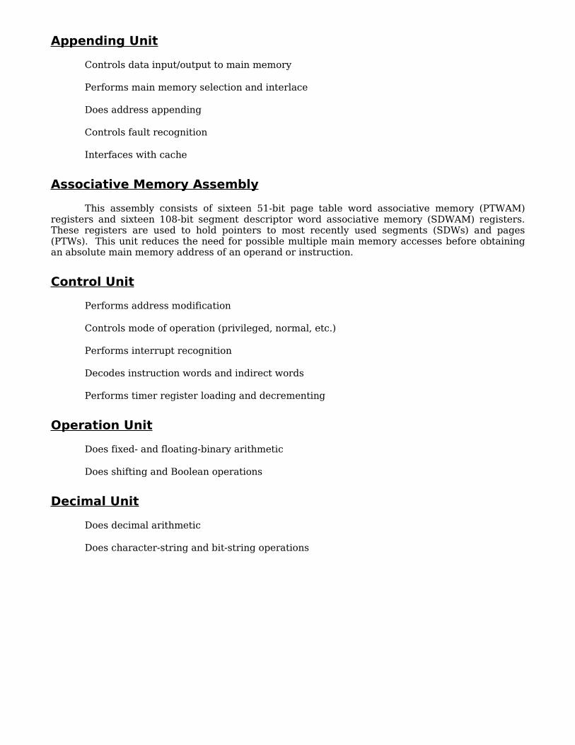
Appending Unit
Controls data input/output to main memory
Performs main memory selection and interlace
Does address appending
Controls fault recognition
Interfaces with cache
Associative Memory Assembly
This assembly consists of sixteen 51-bit page table word associative memory (PTWAM) registers and sixteen 108-bit segment descriptor word associative memory (SDWAM) registers. These registers are used to hold pointers to most recently used segments (SDWs) and pages (PTWs). This unit reduces the need for possible multiple main memory accesses before obtaining an absolute main memory address of an operand or instruction.
Control Unit
Performs address modification
Controls mode of operation (privileged, normal, etc.)
Performs interrupt recognition
Decodes instruction words and indirect words
Performs timer register loading and decrementing
Operation Unit
Does fixed- and floating-binary arithmetic
Does shifting and Boolean operations
Decimal Unit
Does decimal arithmetic
Does character-string and bit-string operations
SECTION 2: DATA REPRESENTATION
INFORMATION ORGANIZATION
The processor, like the rest of the Multics system, is organized to deal with information in basic units of 36-bit words. Other units of 4-, 6-, 9-bit characters or bytes, 18-bit half words, and 72-bit word pairs can be manipulated within the processor by use of the instruction set. These bit groupings are used by the hardware and software to represent a variety of forms of coded data. Certain processor functions appear to manipulate larger units of 144, 288, 576, and 1152 bits, but these functions are performed by means of repeated use of 72-bit word pairs. All information is transmitted, stored, and processed as strings of binary bits. The data values are derived when the bit strings are interpreted according to the various formats discussed in this section.
POSITION NUMBERING
The numbering of bit positions, character and byte positions, and words increases from 0 in the direction of conventional reading and writing: from the most significant to the least significant digit of a number, and from left to right in conventional alphanumeric text.
Graphic presentations in this manual show registers and data with position numbers increasing from left to right.
NUMBER SYSTEM
The binary arithmetic functions of the processor are implemented in the twos complement, binary number system. One of the primary properties of this number system is that a field (or register) having width n bits may be interpreted in two different ways; the logical case and the arithmetic or algebraic case.
In the logical case, the number is unsigned, positive, and lies in the range [0,2n-1] where n is the size of the register or the length of the field. The results of arithmetic operations on numbers for this case are interpreted as modulo 2n numbers. Overflow is not defined for this case since the range of the field or register cannot be exceeded. The numbers 0 and 2n-1 are consecutive (not separated) in the set of numbers defined for the field or register.
In the arithmetic case, the number is signed and lies in the range [-2(n-1),2(n-1)-1]. Overflow is defined for this case since the range can be exceeded in either direction (positive or negative). The left-hand-most bit of the field or register (bit 0) serves as the sign bit and does not contribute to the magnitude of the number.
The main advantage of this implementation is that the hardware arithmetic algorithms for the two cases are identical; the only distinction lying in the interpretation of the results by the user. Instruction set features are provided for performing binary arithmetic with overflow disabled (the so-called logical instructions) and for comparing numbers in either sense.
Subtraction is performed by adding the twos complement of the subtrahend to the minuend. (Note that when the subtrahend is zero the algorithm for forming the twos complement is still carried out, but, since the twos complement of zero is zero, the result is correct.)
Another important feature of the twos complement number system (with respect to comparison of numeric values) is that the no borrow condition in true subtraction is identical to the carry condition in true addition and vice versa.
A statement on the assumed location of the binary point has significance only for multiplication and division. These two operations are implemented for the arithmetic case in both integer and fraction modes. Integer means that the position of the binary point is assumed to the

right of the least significant bit position, that is, to the right of the right-hand-most bit of the field or register, and fraction means that the position of the binary point is assumed to the left of the most significant bit position, that is, between bit 0 and bit 1 of the field or register (recall that bit 0 is the sign bit).
INFORMATION FORMATS
The figures that follow show the unstructured formats (templates) for the various information units defined for the processor. Data transfer between the processor and main memory is word oriented; a 36-bit machine word is transferred for single-precision operands and subfields of machine words, and a 72-bit word pair is transferred for all other cases (multiword operands, instruction fetches, bit- and character-string operands, etc.). The information unit to be used and the data transfer mode are determined by the processor according to the function to be performed.
The 36-bit unstructured machine word shown in Figure 2-1 is the minimum addressable information unit in main memory. Its location is uniquely determined by its main memory address, Y. All other information units are defined relative to the 36-bit machine word.
Figure 2-1. Unstructured Machine Word Format
Two consecutive machine words as shown in Figure 2-2, the first having an even main memory address, form a 72-bit word pair. In 72-bit word pair data transfer mode, the word pair is uniquely located by the main memory address of either of its constituent 36-bit machine words. Thus, if Y is even, the word pair at (Y,Y+1) is selected. If Y is odd, the word pair at (Y-1,Y) is selected. The term Y-pair is used when referring to such a word pair.
Figure 2-2. Unstructured Word Pair Format
Four-bit bytes are mapped onto 36-bit machine words as shown in Figure 2-3. The 0 bits at bit positions 0, 9, 18, and 27 are forced to be 0 by the processor on data transfers to main memory and are ignored on data transfers from main memory.
Figure 2-3. Unstructured 4-bit Byte Format
Six-bit characters are mapped onto 36-bit machine words as shown in Figure 2-4.
00
36
35
00
35
36
36
71
36
Even word Odd word
00
0
1
01
04
4
05
08
4
09
0
1
10
13
4
14
17
4
18
0
1
19
22
4
23
26
4
27
0
1
28
31
4
32
35
4

Figure 2-4. Unstructured 6-bit Character Format
Nine-bit bytes are mapped onto 36-bit machine words as shown in Figure 2-5.
Figure 2-5. Unstructured 9-bit Byte Format
Eighteen-bit half words are mapped onto 36-bit machine words as shown in Figure 2-6.
Figure 2-6. Unstructured 18-bit Half Word Format
DATA PARITY
Odd parity on each 36-bit machine word transferred to main memory is generated as it leaves the processor, is verified at several points along the transmission path, and is held in main memory either as an extra bit in the case of magnetic core memory or as part of the error detecting and correcting (EDAC) code in the case of magnetic oxide semiconductor (MOS) memory. If an incorrect parity is detected at any of the various parity check points, the main memory returns an illegal action signal and a code appropriate to the check point.
On data transfers from main memory, the parity information is retrieved and transmitted with the data information. The same verification checks are made and illegal action signalled for errors. The processor makes a final parity check as the data enters the processor.
Any detected parity error causes the processor parity indicator to be set ON and (if enabled) a parity fault occurs.
REPRESENTATION OF DATA
Data is defined by imposing an operand structure on the information units just described. Data is represented in two forms: numeric or alphanumeric. The form is determined by the processor according to the function to be performed.
In the definitions below, ai is the value of the bit in the ith bit position, either 0 or 1.
00
05
6
06
11
6
12
17
6
18
23
6
24
29
6
30
35
6
00
08
9
09
17
9
18
26
9
27
35
9
Upper half Lower half
00
17
18
18
35
18
Numeric Data
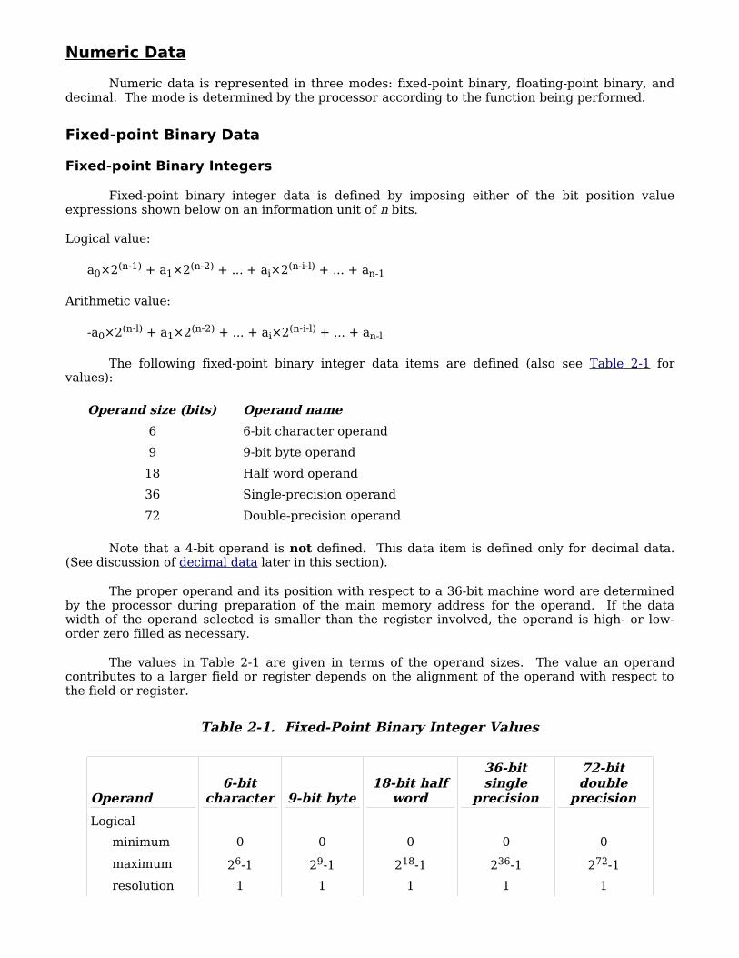
Numeric data is represented in three modes: fixed-point binary, floating-point binary, and decimal. The mode is determined by the processor according to the function being performed.
Fixed-point Binary Data
Fixed-point Binary Integers
Fixed-point binary integer data is defined by imposing either of the bit position value expressions shown below on an information unit of n bits.
Logical value:
a0×2(n-1) + a1×2(n-2) + ... + ai×2(n-i-l) + ... + an-1
Arithmetic value:
-a0×2(n-l) + a1×2(n-2) + ... + ai×2(n-i-l) + ... + an-l
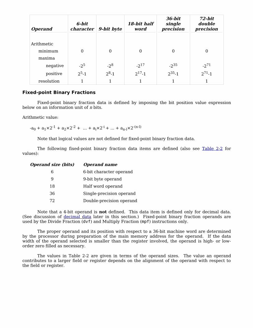
The following fixed-point binary integer data items are defined (also see Table 2-1 for values):
Operand size (bits) Operand name
6 6-bit character operand
9 9-bit byte operand
18 Half word operand
36 Single-precision operand
72 Double-precision operand
Note that a 4-bit operand is not defined. This data item is defined only for decimal data. (See discussion of decimal data later in this section).
The proper operand and its position with respect to a 36-bit machine word are determined by the processor during preparation of the main memory address for the operand. If the data width of the operand selected is smaller than the register involved, the operand is high- or low-order zero filled as necessary.
The values in Table 2-1 are given in terms of the operand sizes. The value an operand contributes to a larger field or register depends on the alignment of the operand with respect to the field or register.
Table 2-1. Fixed-Point Binary Integer Values
Operand6-bit
character 9-bit byte18-bit half
word
36-bit single
precision
72-bit double
precision
Logical
minimum 0 0 0 0 0
maximum 26-1 29-1 218-1 236-1 272-1
resolution 1 1 1 1 1
Operand6-bit
character 9-bit byte18-bit half
word
36-bit single
precision
72-bit double
precision
Arithmetic
minimum 0 0 0 0 0
maxima
negative -25 -28 -217 -235 -271
positive 25-1 28-1 217-1 235-1 271-1
resolution 1 1 1 1 1
Fixed-point Binary Fractions
Fixed-point binary fraction data is defined by imposing the bit position value expression below on an information unit of n bits.
Arithmetic value:
-a0 + a1×2-1 + a2×2-2 + ... + ai×2-i + ... + an-l×2-(n-l)
Note that logical values are not defined for fixed-point binary fraction data.
The following fixed-point binary fraction data items are defined (also see Table 2-2 for values):
Operand size (bits) Operand name
6 6-bit character operand
9 9-bit byte operand
18 Half word operand
36 Single-precision operand
72 Double-precision operand
Note that a 4-bit operand is not defined. This data item is defined only for decimal data. (See discussion of decimal data later in this section.) Fixed-point binary fraction operands are used by the Divide Fraction (dvf) and Multiply Fraction (mpf) instructions only.
The proper operand and its position with respect to a 36-bit machine word are determined by the processor during preparation of the main memory address for the operand. If the data width of the operand selected is smaller than the register involved, the operand is high- or low-order zero filled as necessary.
The values in Table 2-2 are given in terms of the operand sizes. The value an operand contributes to a larger field or register depends on the alignment of the operand with respect to the field or register.
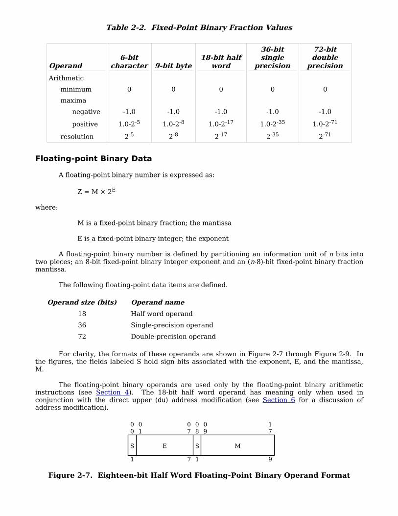
Table 2-2. Fixed-Point Binary Fraction Values
Operand6-bit
character 9-bit byte18-bit half
word
36-bit single
precision
72-bit double
precision
Arithmetic
minimum 0 0 0 0 0
maxima
negative -1.0 -1.0 -1.0 -1.0 -1.0
positive 1.0-2-5 1.0-2-8 1.0-2-17 1.0-2-35 1.0-2-71
resolution 2-5 2-8 2-17 2-35 2-71
Floating-point Binary Data
A floating-point binary number is expressed as:
Z = M × 2E
where:
M is a fixed-point binary fraction; the mantissa
E is a fixed-point binary integer; the exponent
A floating-point binary number is defined by partitioning an information unit of n bits into two pieces; an 8-bit fixed-point binary integer exponent and an (n-8)-bit fixed-point binary fraction mantissa.
The following floating-point data items are defined.
Operand size (bits) Operand name
18 Half word operand
36 Single-precision operand
72 Double-precision operand
For clarity, the formats of these operands are shown in Figure 2-7 through Figure 2-9. In the figures, the fields labeled S hold sign bits associated with the exponent, E, and the mantissa, M.
The floating-point binary operands are used only by the floating-point binary arithmetic instructions (see Section 4). The 18-bit half word operand has meaning only when used in conjunction with the direct upper (du) address modification (see Section 6 for a discussion of address modification).
Figure 2-7. Eighteen-bit Half Word Floating-Point Binary Operand Format
00
S
1
01
E
07
7
08
S
1
09
M
17
9

Figure 2-8. Single-Precision Floating-Point Binary Operand Format
Figure 2-9. Double-Precision Floating-Point Binary Operand Format
The proper operand is selected by the processor during preparation of the main memory address for the operand.
Overlength Registers
The AQ-register is used to hold the mantissa of all floating-point binary numbers. The AQ-register is said to be overlength with respect to the operands since it has more bits than are provided by the operands. Operands are low-order zero filled when loaded and low-order truncated (or rounded, depending on the instruction) when stored. Thus, the result of all floating-point instructions has more bits of precision in the AQ-register than may be stored.
Users are cautioned that calculations involving floating-point operands may suffer from propagation of truncation errors even if the computation algorithms are designed to hold mantissas in the AQ-register as long as possible. It is possible to retain full AQ-register precision of intermediate results if they are saved with the Store AQ (staq) and Store Exponent (ste) instructions but such saved data are not usable as a floating-point operand.
Normalized Numbers
A floating-point binary number is said to be normalized if the relation
-0.5 > M > -1 or 0.5 ≤ M < 1 or [M=0 and E=-128]
is satisfied. This is a result of using a 2's complement mantissa. Bits 8 and 9 are different unless the number is zero. The presence of unnormalized numbers in any finite mantissa arithmetic can only degrade the accuracy of results. For example, in an arithmetic allowing only two digits in the mantissa, the number 0.005×10² has the value zero instead of the value one-half.
Normalization is a process of shifting the mantissa and adjusting the exponent until the relation above is satisfied. Normalization may be used to recover some or all of the extra bits of the overlength AQ-register after a floating-point operation.
There are cases where the limits of the registers force the use of unnormalized numbers. For example, in an arithmetic allowing three digits of mantissa and one digit of exponent, the calculation 0.3×10⁻¹⁰ - 0.1×10⁻¹¹ (the normalized case) may not be made, but 0.03×10⁻⁹ – 0.001×10-9 = 0.029×10⁻⁹ (the unnormalized case) is a valid result.
Some examples of normalized and unnormalized floating-point binary numbers are:
Unnormalized positive binary 0.00011010 × 27
00
S
1
01
E
07
7
08
S
1
09
M
35
27
00
S
1
01
E
07
7
08
S
1
09
M
71
63
Same number normalized 0.11010000 × 24
Unnormalized negative binary 1.11010111 × 2-4
Same number normalized 1.01011100 × 2-6
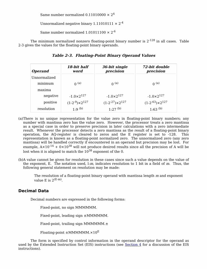
The minimum normalized nonzero floating-point binary number is 2-128 in all cases. Table 2-3 gives the values for the floating-point binary operands.
Table 2-3. Floating-Point Binary Operand Values
Operand18-bit half
word36-bit single
precision72-bit double
precision
Unnormalized
minimum 0 (a) 0 (a) 0 (a)
maxima
negative -1.0×2127 -1.0×2127 -1.0×2127
positive (1-2-9)×2127 (1-2-27)×2127 (1-2-63)×2127
resolution 1:9 (b) 1:27 (b) 1:63 (b)
(a)There is no unique representation for the value zero in floating-point binary numbers; any number with mantissa zero has the value zero. However, the processor treats a zero mantissa as a special case in order to preserve precision in later calculations with a zero intermediate result. Whenever the processor detects a zero mantissa as the result of a floating-point binary operation, the AQ-register is cleared to zeros and the E register is set to -128. This representation is known as a floating-point normalized zero. The unnormalized zero (any zero mantissa) will be handled correctly if encountered in an operand but precision may be lost. For example, A×10-14 + 0×1038 will not produce desired results since all the precision of A will be lost when it is aligned to match the 1038 exponent of the 0.
(b)A value cannot be given for resolution in these cases since such a value depends on the value of the exponent, E. The notation used, l:m, indicates resolution to 1 bit in a field of m. Thus, the following general statement on resolution may be made:
The resolution of a floating-point binary operand with mantissa length m and exponent value E is 2(E-m).
Decimal Data
Decimal numbers are expressed in the following forms:
Fixed-point, no sign MMMMMM.
Fixed-point, leading sign ±MMMMMM.
Fixed-point, trailing sign MMMMMM.±
Floating-point ±MMMMMM.×10E
The form is specified by control information in the operand descriptor for the operand as used by the Extended Instruction Set (EIS) instructions (see Section 4 for a discussion of the EIS instructions).
A decimal number is defined by imposing any of the byte position value expressions below on a 4- or 9-bit byte information unit of length n bytes.
Fixed-point, no sign:
c0×10(n-1) + c1×10(n-2) + ... + c(n-1)
Fixed-point, leading sign:
[sign=c0] c1×10(n-2) + c2×10(n-3) + ... + c(n-1)
Fixed-point, trailing sign:
c0×10(n-2) + c1×10(n-3) + ... + c(n-2) [sign=c(n-1)]
Floating-point:
[sign=c0] c1×10(n-3) + c2×10(n-4) + ... + c(n-3) [exponent=8 bits]
where:
ci is the decimal value of the byte in the ith byte position.
[sign=ci] indicates that ci is interpreted as a sign byte.
[exponent=8 bits] indicates that the exponent value is taken from the last 8 bits of the string. If the data is in 9-bit bytes, the exponent is bits 1-8 of c(n-1). If the data is in 4-bit bytes, the exponent is the binary value of the concatenation of c(n-2) and c(n-1).
The decimal number as described above is the only decimal data item defined. It may begin on any legal byte boundary (without regard to word boundaries) and has a maximum extent of 63 bytes.
The processor handles decimal data as 4-bit bytes internally. Thus, 9-bit bytes are high-order truncated as they are transferred from main memory and high-order filled as they are transferred to main memory. The fill pattern is "00011"b for digit bytes and "00010" for sign bytes. The floating-point exponent is a special case and is treated as a fixed-point binary integer.
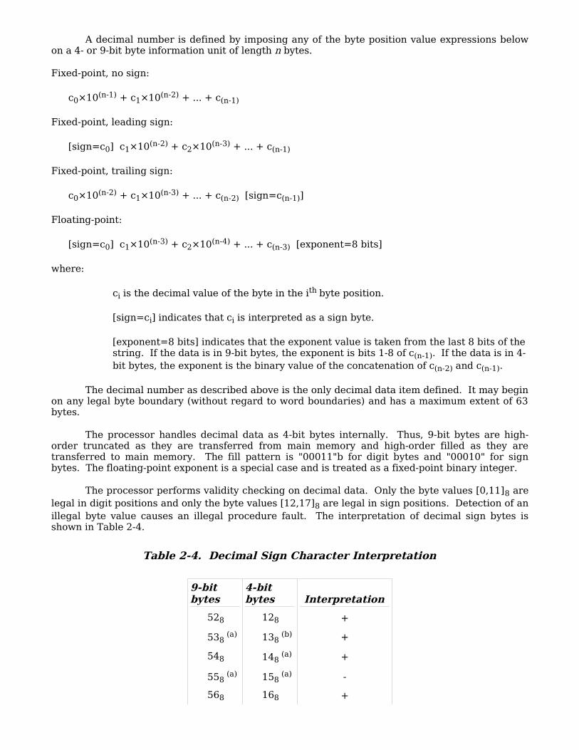
The processor performs validity checking on decimal data. Only the byte values [0,11]8 are legal in digit positions and only the byte values [12,17]8 are legal in sign positions. Detection of an illegal byte value causes an illegal procedure fault. The interpretation of decimal sign bytes is shown in Table 2-4.
Table 2-4. Decimal Sign Character Interpretation
9-bit bytes
4-bit bytes Interpretation
528 128 +
538 (a) 138
(b) +
548 148 (a) +
558 (a) 158
(a) -
568 168 +

9-bit bytes
4-bit bytes Interpretation
578 178 +
(a)This value is used as the default sign byte for storage of results. The presence of other values will yield correct results according to the interpretation.
(b)An optional control bit in the EIS decimal arithmetic instructions (see Section 4) allows the selection of 138 for the plus sign byte for storage of results in 4-bit data mode.
Decimal Data Values
The operand descriptors for decimal data operands have a 6-bit fixed-point binary integer field for specification of a scaling factor (SF). This scaling factor has the same effect as the value of E in floating-point decimal operands; a negative value moves the assumed decimal point to the left; a positive value, to the right. The use of the scaling factor extends the range and resolution of decimal data operands. The range of the scaling factor is [-32,31]10. See Table 2-5 for decimal data operand values.
Table 2-5. Decimal Data Values
OperandFixed-point unsigned
Fixed-point signed
Floating-point 9 bit
Floating-point 4 bit
Arithmetic
minimum 0 0 (a) 0 (a) 0 (a)
maximum (1063-1)×1031 ±(1062-1)×1031 ±(1061-1)×10158 ±(1060-1)×10158
resolution 1:SF (b) 1:SF (b) 1:E (c) 1:E (c)
(a)As in floating-point binary arithmetic, there is no unique representation of the value zero except in the case of fixed-point, unsigned data. Therefore, the processor detects a zero result and forces a value of +0. for fixed-point, signed data and +0.×10127 for floating-point data. Again, as in floating-point binary arithmetic, other representations of the value zero will be handled correctly except for possible loss of precision during operand alignment.
(b)A value cannot be given for resolution in these cases since such a value depends on the value of the scaling factor, SF. The notation used, 1:SF, indicates resolution to 1 part in 10(SF). Thus, the following general statement on resolution may be made:
The resolution of a fixed-point decimal operand with scaling factor SF is 10SF.
(c)A value cannot be given for resolution in these cases since such a value depends on the value of the exponent, E. The notation used, 1:E, indicates resolution to 1 part in 10(E). Thus, the following general statement on resolution may be made:
The resolution of a floating-point decimal operand with exponent E is 10(E).
The scaling factor is ignored by the hardware.
Alphanumeric Data
Alphanumeric data is represented in two modes; character-string and bit-string. The mode is determined by the processor according to the function being performed.

Character String Data
Character string data is defined by imposing the character position structure below on a 4-bit, 6-bit, or 9-bit information unit of length n bytes or characters.
c0 || c1 || ... || c(n-1)
where:
ci is the character in the ith character position.
|| indicates the concatenation operation.
The character string described above is the only character string data item defined. It may begin on any legal character boundary (without regard to word boundaries) and has a maximum extent as shown in Table 2-6.
Table 2-6. Character String Data Length Limits
Character size Length limit
9-bit 1048576
6-bit 1572864
4-bit 2097152
No interpretation of the characters is made except as specified for the instruction being executed (see Section 4).
Bit String Data
Bit string data is defined by imposing the bit position structure below on a bit information unit of length n bits.
b0 || b1 || ... || b(n-1)
where:
bi is the value of the bit in the ith position.
|| indicates the concatenation operation.
The bit string described above is the only bit string data item defined. It may begin at any bit position (without regard to character or word boundaries) and has a maximum extent of 9437184 bits.
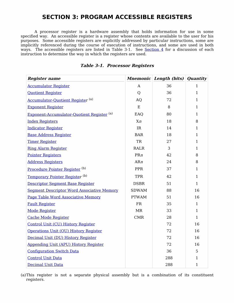
SECTION 3: PROGRAM ACCESSIBLE REGISTERS
A processor register is a hardware assembly that holds information for use in some specified way. An accessible register is a register whose contents are available to the user for his purposes. Some accessible registers are explicitly addressed by particular instructions, some are implicitly referenced during the course of execution of instructions, and some are used in both ways. The accessible registers are listed in Table 3-1. See Section 4 for a discussion of each instruction to determine the way in which the registers are used.
Table 3-1. Processor Registers
Register name Mnemonic Length (bits) Quantity
Accumulator Register A 36 1
Quotient Register Q 36 1
Accumulator-Quotient Register (a) AQ 72 1
Exponent Register E 8 1
Exponent-Accumulator-Quotient Register (a) EAQ 80 1
Index Registers Xn 18 8
Indicator Register IR 14 1
Base Address Register BAR 18 1
Timer Register TR 27 1
Ring Alarm Register RALR 3 1
Pointer Registers PRn 42 8
Address Registers ARn 24 8
Procedure Pointer Register (b) PPR 37 1
Temporary Pointer Register (b) TPR 42 1
Descriptor Segment Base Register DSBR 51 1
Segment Descriptor Word Associative Memory SDWAM 88 16
Page Table Word Associative Memory PTWAM 51 16
Fault Register FR 35 1
Mode Register MR 33 1
Cache Mode Register CMR 28 1
Control Unit (CU) History Register 72 16
Operations Unit (OU) History Register 72 16
Decimal Unit (DU) History Register 72 16
Appending Unit (APU) History Register 72 16
Configuration Switch Data 36 5
Control Unit Data 288 1
Decimal Unit Data 288 1
(a)This register is not a separate physical assembly but is a combination of its constituent registers.
(b)This register is not explicitly addressable, but is included because of its vital role in instruction and operand address preparation.
In the descriptions that follow, the diagrams given for register formats do not imply that a physical assembly possessing the pictured bit pattern exists. The diagram is a graphic representation of the form of the register data as it appears in main memory when the register contents are stored or how data bits must be assembled for loading into the register.
If the diagrams contain the characters "x" or "0", the values of the bits in the positions shown are irrelevant to the register. Bits pictured as "x" are not changed when the register is stored. Bits pictured as "0" are set to 0 when the register is stored. Neither "x" bits or "0" bits are loaded into the register.
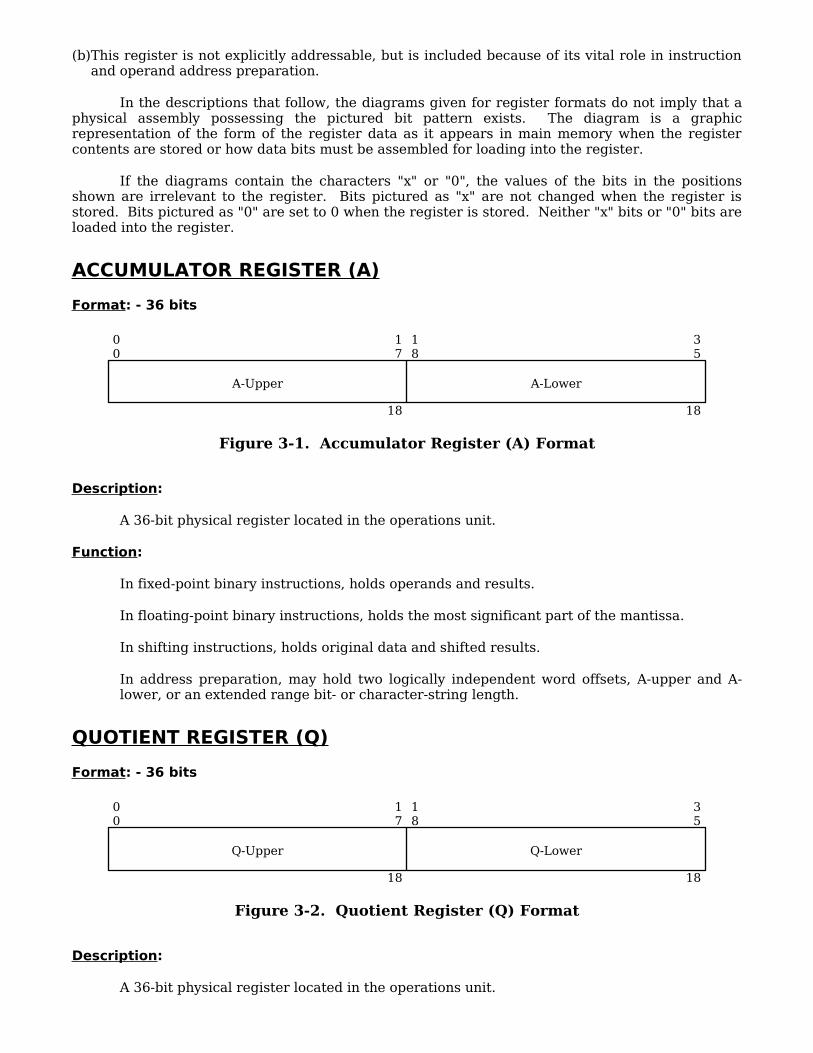
ACCUMULATOR REGISTER (A)
Format: - 36 bits
Figure 3-1. Accumulator Register (A) Format
Description:
A 36-bit physical register located in the operations unit.
Function:
In fixed-point binary instructions, holds operands and results.
In floating-point binary instructions, holds the most significant part of the mantissa.
In shifting instructions, holds original data and shifted results.
In address preparation, may hold two logically independent word offsets, A-upper and A-lower, or an extended range bit- or character-string length.
QUOTIENT REGISTER (Q)
Format: - 36 bits
Figure 3-2. Quotient Register (Q) Format
Description:
A 36-bit physical register located in the operations unit.
A-Upper A-Lower
00
17
18
18
35
18
Q-Upper Q-Lower
00
17
18
18
35
18

Function:
In fixed-point binary instructions, holds operands and results.
In floating-point binary instructions, holds the least significant part of the mantissa.
In shifting instructions, holds original data and shifted results.
In address preparation, may hold two logically independent word offsets, Q-upper and Q-lower, or an extended range bit- or character-string length.
ACCUMULATOR-QUOTIENT REGISTER (AQ)
Format: - 72 bits
Figure 3-3. Accumulator-Quotient Register (AQ) Format
Description:
A combination of the accumulator (A) and quotient (Q) registers.
Function:
In fixed-point binary instructions, holds double-precision operands and results.
In floating-point binary instructions, holds the mantissa.
In shifting instructions, holds original data and shifted results.
EXPONENT REGISTER (E)
Format: - 8 bits
Figure 3-4. Exponent Register (E) Format
Description:
An 8-bit physical register located in the operations unit.
Function:
In floating-point binary instructions, holds the exponent.
Even word Odd word
A Q
00
35
36
36
71
36
00
8
07
08
0 0 0 0 0 0 0 0 0 0 0 0 0 0 0 0 0 0 0 0 0 0 0 0 0 0 0
35
0
28
exponent

EXPONENT-ACCUMULATOR-QUOTIENT REGISTER (EAQ)
Format: - 80 bits
Figure 3-5. Exponent-Accumulator-Quotient Register (EAQ) Format
Description:
A combination of the exponent (E), accumulator (A), and quotient (Q) registers. Although the combined register has a total of 80 bits, only 72 are involved in transfers to and from main memory. The 8 low-order bits are discarded on store and zero-filled on load.
Function:
In floating-point binary instructions, holds operands and results.
INDEX REGISTERS (X n )
Format: - 18 bits each
Figure 3-6. Index Register (Xn) Format
Description:
Eight 18-bit physical registers in the operations unit numbered 0 through 7. Index register data may occupy the position of either an upper or lower 18-bit half-word operand (see Section 2).
Function:
In fixed-point binary instructions, hold half-word operands and results.
In address preparation, hold word offsets or extended range bit- or character-string lengths.
00
8
07
08
71
64
exponent mantissa
00
17
18

INDICATOR REGISTER (IR)
Format: - 14 bits
Figure 3-7. Indicator Register (IR) Format
Description:
An assemblage of 15 indicator flags from various units of the processor. The data occupies the position of a lower 18-bit half word operand (see Section 2). When interpreted as data, a bit value of 1 corresponds to the ON state of the indicator, a bit value of 0 corresponds to the OFF state.
Function:
The functions of the individual indicator bits are given below. An "x" in the column headed "L" indicates that the state of the indicator is not affected by instructions that load the IR.
key L Indicator name Action
a Zero This indicator is set ON whenever the output of the main binary adder consists entirely of zero bits for binary or shifting instructions or the output of the decimal adder consists entirely of zero digits for decimal instructions; otherwise, it is set OFF.
b Negative This indicator is set ON whenever the output of bit 0 of the main binary adder has value 1 for binary or shifting instructions or the sign character of the result of a decimal instruction is the negative sign character; otherwise, it is set OFF.
c Carry This indicator is set ON for any of the following conditions; otherwise, it is set OFF.
(1) If a bit propagates leftward out of bit 0 of the main binary adder for any binary or shifting instruction.
(2) If | value1 | <= | value2 | for a decimal numeric comparison instruction.
(3) If char1 <= char2 for a decimal alphanumeric compare instruction.
d Overflow This indicator is set ON if the arithmetic range of a register is exceeded in a fixed-point binary instruction or if the target string of a decimal numeric instruction is too small to hold the integer part of the result. It remains ON until reset by the Transfer On Overflow (tov) instruction or is reset by some other instruction that loads the IR. The event that sets this indicator ON may also cause an overflow fault. (See overflow mask indicator below.)
00
x x x x x x x x x x x x x x x x x
17
x
18
18
a
1
19
b
1
20
c
1
21
d
1
22
e
1
23
f
1
24
g
1
25
h
1
26
i
1
27
j
1
28
k
1
29
l
1
30
m
1
31
n
1
32
o
1
0 0
35
0
3

key L Indicator name Action
e Exponent overflow
This indicator is set ON if the exponent of the result of a floating-point binary or decimal numeric instruction is greater than +127. It remains ON until reset by the Transfer On Exponent Overflow (teo) instruction or is reset by some other instruction that loads the IR. The event that sets this indicator ON may also cause an overflow fault. (See overflow mask indicator below.)
f Exponent underflow
This indicator is set ON if the exponent of the result of a floating-point binary or decimal numeric instruction is less than -128. It remains ON until reset by the Transfer On Exponent Underflow (teu) instruction or is reset by some other instruction that loads the IR. The event that sets this indicator ON may also cause an overflow fault. (See overflow mask indicator below.)
g Overflow mask This indicator is set ON or OFF only by the instructions that load the IR. When set ON, the IR inhibits the generation of the fault for those events that normally cause an overflow fault. If the overflow mask indicator is set OFF after occurrence of an overflow event, an overflow fault does not occur even though the indicator for that event is still set ON. The state of the overflow mask indicator does not affect the setting, testing, or storing of any other indicator.
h Tally runout This indicator is set OFF at initialization of any tallying operation, that is, any repeat instruction or any indirect then tally address modification. It is then set ON for any of the following conditions:
(1) If any repeat instruction terminates because of tally exhaust.
(2) If a Repeat Link (rpl) instruction terminates because of a zero link address.
(3) If a tally exhaust is detected for an indirect then tally modifier. The instruction is executed whether or not tally exhaust occurs.
(4) If an EIS string scanning instruction reaches the end of the string without finding a match condition.
i Parity error This indicator is set ON whenever a system controller signals illegal action with a parity error code or the processor detects an internal parity error condition. The indicator is set OFF only by instructions that load the IR.
j Parity mask This indicator is set ON or OFF only by the instructions that load the IR and is changed only when the processor is in privileged or absolute mode. When it is set ON, the IR inhibits the generation of the parity fault for all events that set the parity error indicator. If the parity mask indicator is set OFF after the occurrence of a parity error event, a parity fault does not occur even though the parity error indicator may still be set ON. The state of the parity mask indicator does not affect the loading, testing, or storing of any other indicator.

key L Indicator name Action
k x Not BAR mode This indicator is set OFF (placing the processor in BAR mode) only by execution of the Transfer and Set Slave (tss) instruction or by the operand data of the Restore Control Unit (rcu) instruction and is changed only when the processor is in privileged or absolute mode. It is set ON (taking the processor out of BAR node) by the execution of any transfer instruction other than tss during a fault or interrupt trap. (See Section 7.) If a fault or interrupt trap occurs while in BAR node and the IR is stored before any transfer occurs, then a Return (ret) or Restore Control Unit (rcu) instruction that reloads the stored data will return the processor to BAR mode.
l Truncation This indicator is set ON whenever the target string of a decimal numeric instruction is too small to hold all the digits of the result or the target string of an alphanumeric instruction is too small to hold all the bits or characters to be stored. (Also see the overflow indicator for decimal numeric instructions.) The event that sets this indicator ON may also cause an overflow fault. (See overflow mask indicator above.)
m Mid instruction interrupt fault
This indicator is set OFF at the start of execution of each instruction and is set ON by the events described below. The indicator has meaning only when determining the proper restart sequence for the interrupted instruction. This indicator can be set on:
(1) By any fault during execution of an EIS instruction; however, the state is safe-stored in the Control Unit Data only for access violation and directed faults.
(2) By an interrupt signal during execution of those EIS instructions that allow very long operand strings.
(3) If the processor is in absolute or privileged mode, by the execution of a Load Indicator Register (ldi), Return (ret), or Restore Control Unit (rcu) instruction with bit 30 set to 1 in the IR data.
n x Absolute mode This indicator is set ON (placing the processor in absolute mode) when the processor is initialized and by execution of an nonappended transfer instruction during a fault or interrupt trap and is set OFF (placing the processor in append mode) by any execution of an appended transfer instruction. If the processor is not in absolute mode when the fault or interrupt occurs and the transfer instruction is Return (ret) or Restore Control Unit (rcu) and the appropriate mode bit is properly set in the IR data, the processor remains in its current mode.
o Hex mode When the hexadecimal permission indicator (bit 33 of the Mode Register) is set on and this indicator is also on, then the exponent of a floating point number has a power of 16 rather than a power of two (binary floating point). The state of the hex mode indicator can be changed by executing a Load Indicator Register (ldi), Return (ret), or Restore Control Unit (rcu), instruction with the desired state (1 or 0) set in bit 32 of the IR data. Hexadecimal mode is only available on DPS 8M processors. Indicator Register bit 32 is set to a zero value on DPS/L68 processors.
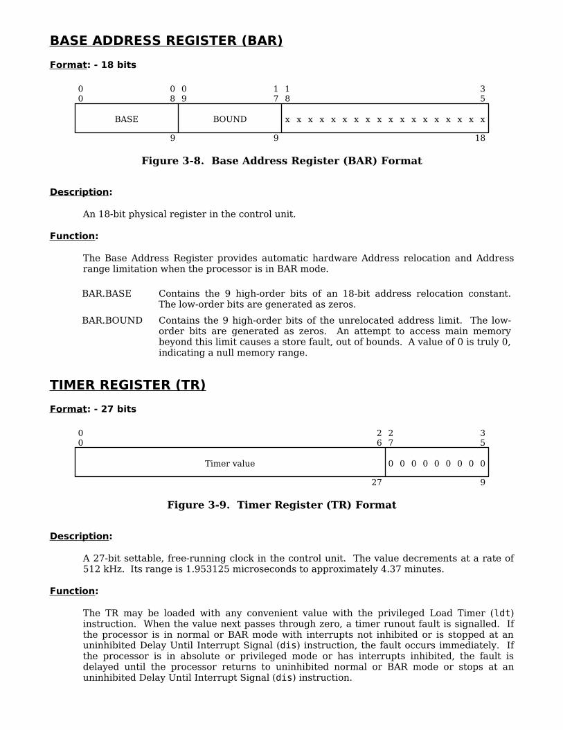
BASE ADDRESS REGISTER (BAR)
Format: - 18 bits
Figure 3-8. Base Address Register (BAR) Format
Description:
An 18-bit physical register in the control unit.
Function:
The Base Address Register provides automatic hardware Address relocation and Address range limitation when the processor is in BAR mode.
BAR.BASE Contains the 9 high-order bits of an 18-bit address relocation constant. The low-order bits are generated as zeros.
BAR.BOUND Contains the 9 high-order bits of the unrelocated address limit. The low-order bits are generated as zeros. An attempt to access main memory beyond this limit causes a store fault, out of bounds. A value of 0 is truly 0, indicating a null memory range.
TIMER REGISTER (TR)
Format: - 27 bits
Figure 3-9. Timer Register (TR) Format
Description:
A 27-bit settable, free-running clock in the control unit. The value decrements at a rate of 512 kHz. Its range is 1.953125 microseconds to approximately 4.37 minutes.
Function:
The TR may be loaded with any convenient value with the privileged Load Timer (ldt) instruction. When the value next passes through zero, a timer runout fault is signalled. If the processor is in normal or BAR mode with interrupts not inhibited or is stopped at an uninhibited Delay Until Interrupt Signal (dis) instruction, the fault occurs immediately. If the processor is in absolute or privileged mode or has interrupts inhibited, the fault is delayed until the processor returns to uninhibited normal or BAR mode or stops at an uninhibited Delay Until Interrupt Signal (dis) instruction.
00
08
9
09
17
9
18
x x x x x x x x x x x x x x x x x
35
x
18
BASE BOUND
00
26
27
27
0 0 0 0 0 0 0 0
35
0
9
Timer value

RING ALARM REGISTER (RALR)
Format: - 3 bits
Figure 3-10. Ring Alarm Register (RALR) Format
Description:
A 3-bit physical register in the appending unit.
Function:
If the RALR contains a value other than zero and the effective ring number (see TPR.TRR below) is greater than or equal to the contents of the RALR and the instruction for which an absolute main memory address is being prepared is a transfer instruction, an access violation, ring alarm, fault occurs. Operating system software may use this register to detect crossings from inner rings to outer rings.
POINTER REGISTERS (PR n )
Format: - 42 bits each
Even word of ITS pointer pair
Odd word of ITS pointer pair
00
0 0 0 0 0 0 0 0 0 0 0 0 0 0 0 0 0 0 0 0 0 0 0 0 0 0 0 0 0 0 0 0
32
0
33
33
RALR
35
3
15
00
0 0
02
0
3
03
17
18
SNR
20
3
21
0 0 0 0 0 0 0 0
29
0
9
30
(43)8
35
6
RNR
36
53
18
54
0 0
56
0
3
57
62
6
63
0 0
65
0
3
66
71
6
(TAG)BITNOWORDNO

Data as stored by Store Pointer Register n Packed (sprpn)
Figure 3-11. Pointer Register (PRn) Format
Description:
Eight combinations of physical registers from the appending unit and decimal unit numbered 0 through 7. PRn.RNR, PRn.SNR, and PRn.BITNO are located in the appending unit and PRn.WORDNO is located in the decimal unit. The WORDNO registers also form part of the address registers discussed later in this section.
Function:
The pointer registers hold information relative to the location in main memory of data items that may be external to the segment containing the procedure being executed. The functions of the individual constituent registers are:
Register Function
PRn.SNR The segment number of the segment containing the data item described by the pointer register.
PRn.RNR The final effective ring number value calculated during execution of the instruction that last loaded the PR.
(43)8 This field is not part of the PR but is generated each time the PR is stored as an ITS pair.
PRn.WORDNO The offset in words from the base or origin of the segment to the data item.
PRn.BITNO The number of the bit within PRn.WORDNO that is the first bit of the data item. Data items aligned on word boundaries always have the value 0. Unaligned data items may have any value in the range [1,35].
(TAG) This field is not part of the PR but, in an ITS pointer pair, holds an address modifier for use in address preparation.
ADDRESS REGISTERS (AR n )
Format: - 24 bits each
Data as stored by Store Address Register n (sarn)
Figure 3-12. Address Register (ARn) Format
00
05
6
06
17
WORDNO
12
18
35
18
SNRBITNO
00
17
18
18
a
19
2
20
23
BITNO
4
24
0 0 0 0 0 0 0 0 0 0 0
35
0
12
WORDNO

Description:
Eight combinations of physical registers from the decimal unit numbered 0 through 7. The WORDNO registers also form part of the pointer registers discussed earlier in this section.
Function:
The address registers hold information relative to the location in main memory of the next bit, character, or byte of an EIS operand to be processed by an EIS instruction. The functions of the individual constituent registers are:
key Register Function
ARn.WORDNO The offset in words relative to the current addressing base referent (segment origin, BAR.BASE, or absolute 0 depending on addressing mode) to the word containing the next data item element.
a ARn.CHAR The number of the 9-bit byte within ARn.WORDNO containing the first bit of the next data item element.
ARn.BITNO The number of the bit within ARn.CHAR that is the first bit of the next data item element.
NOTE: The reader's attention is directed to the presence of two bit number registers, PRn.BITNO and ARn.BITNO. Because the Multics processor was implemented as an enhancement to an existing design, certain apparent anomalies appear. One of these is the difference in the handling of unaligned data items by the appending unit and decimal unit. The decimal unit handles all unaligned data items with a 9-bit byte number and bit offset within the byte. Conversion from the description given in the EIS operand descriptor is done automatically by the hardware. The appending unit maintains compatibility with the earlier generation Multics processor by handling all unaligned data items with a bit offset from the prior word boundary; again with any necessary conversion done automatically by the hardware. Thus, a pointer register, PRn, may be loaded from an ITS pointer pair having a pure bit offset and modified by one of the EIS address register instructions (a4bd, s9bd, etc.) using character displacement counts. The automatic conversion performed ensures that the pointer register, PRi, and its matching address register, ARi, both describe the same physical bit in main memory.
SPECIAL NOTICE: The decimal unit has built-in hardware checks for illegal bit offset values but the appending unit does not except for a single case for packed pointers. See NOTES for Load Packed Pointers (lprpn) in Section 4.
PROCEDURE POINTER REGISTER (PPR)
Format: - 37 bits
Shown as part of word 0 of control unit data
00
PRR
02
3
03
PSR
17
15
18
P
1
Other control unit data

Shown as part of word 4 of control unit data
Figure 3-13. Procedure Pointer Register (PPR) Format
Description:
A combination of physical registers from the appending unit and the control unit. PPR.PRR, PPR.PSR, and PPR.P are located in the appending unit and PPR.IC is located in the control unit. The PPR is not explicitly addressable but its data is extracted and stored as part of the data stored with the Store Control Unit (scu) and Store Control Double (stcd) instructions. It is loaded from the control unit data with the Restore Control Unit (rcu) instruction.
Function:
The Procedure Pointer Register holds information relative to the location in main memory of the procedure segment in execution and the location of the current instruction within that segment. The functions of the individual constituent registers are:
Register Function
PPR.PRR The number of the ring in which the process is executing. It is set to the effective ring number of the procedure segment when control is transferred to the procedure.
PPR.PSR The segment number of the procedure being executed.
PPR.P A flag controlling execution of privileged instructions. Its value is 1 (permitting execution of privileged instructions) if PPR.PRR is 0 and the privileged bit in the segment descriptor word (SDW.P) for the procedure is 1; otherwise, its value is 0.
PPR.IC The word offset from the origin of the procedure segment to the current instruction.
TEMPORARY POINTER REGISTER (TPR)
Format: - 42 bits
Shown as part of word 2 of control unit data
00
IC
17
18
Other control unit data
00
TRR
02
3
03
TSR
17
15
Other control unit data
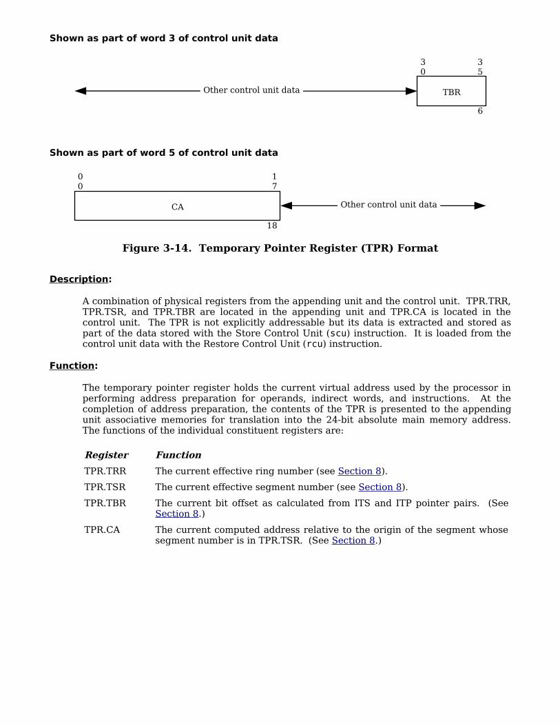
Shown as part of word 3 of control unit data
Shown as part of word 5 of control unit data
Figure 3-14. Temporary Pointer Register (TPR) Format
Description:
A combination of physical registers from the appending unit and the control unit. TPR.TRR, TPR.TSR, and TPR.TBR are located in the appending unit and TPR.CA is located in the control unit. The TPR is not explicitly addressable but its data is extracted and stored as part of the data stored with the Store Control Unit (scu) instruction. It is loaded from the control unit data with the Restore Control Unit (rcu) instruction.
Function:
The temporary pointer register holds the current virtual address used by the processor in performing address preparation for operands, indirect words, and instructions. At the completion of address preparation, the contents of the TPR is presented to the appending unit associative memories for translation into the 24-bit absolute main memory address. The functions of the individual constituent registers are:
Register Function
TPR.TRR The current effective ring number (see Section 8).
TPR.TSR The current effective segment number (see Section 8).
TPR.TBR The current bit offset as calculated from ITS and ITP pointer pairs. (See Section 8.)
TPR.CA The current computed address relative to the origin of the segment whose segment number is in TPR.TSR. (See Section 8.)
30
35
TBR
6
Other control unit data
00
CA
17
18
Other control unit data
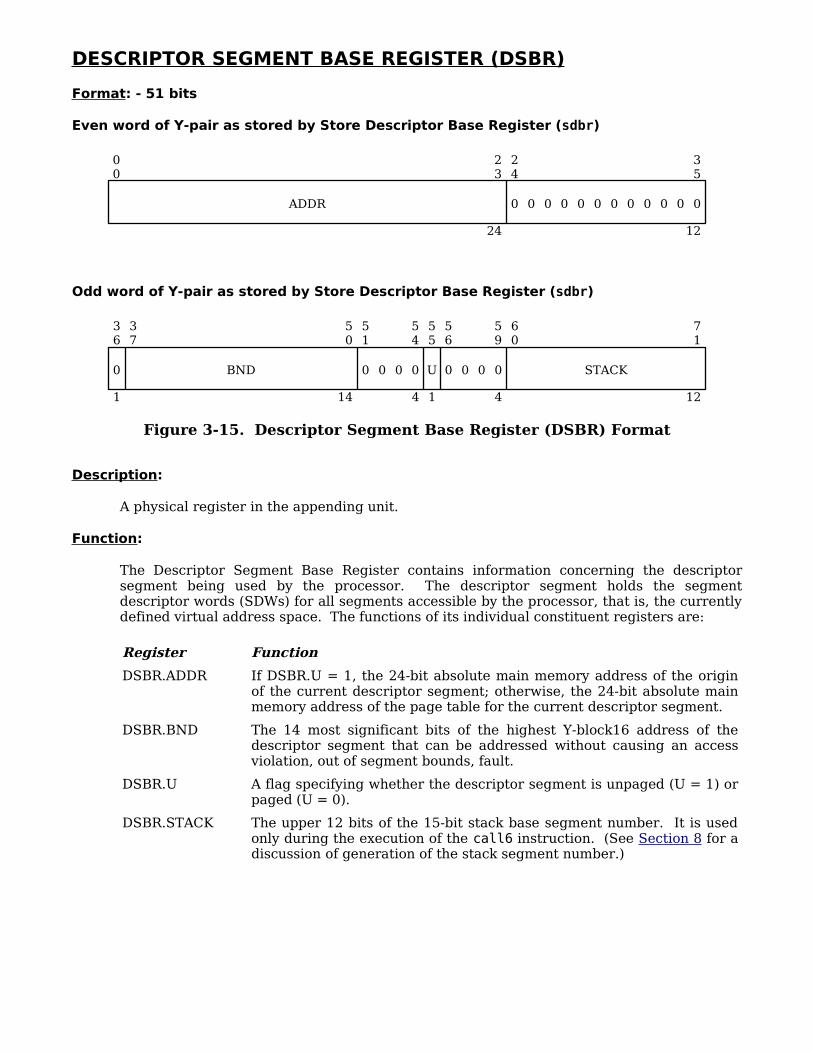
DESCRIPTOR SEGMENT BASE REGISTER (DSBR)
Format: - 51 bits
Even word of Y-pair as stored by Store Descriptor Base Register (sdbr)
Odd word of Y-pair as stored by Store Descriptor Base Register (sdbr)
Figure 3-15. Descriptor Segment Base Register (DSBR) Format
Description:
A physical register in the appending unit.
Function:
The Descriptor Segment Base Register contains information concerning the descriptor segment being used by the processor. The descriptor segment holds the segment descriptor words (SDWs) for all segments accessible by the processor, that is, the currently defined virtual address space. The functions of its individual constituent registers are:
Register Function
DSBR.ADDR If DSBR.U = 1, the 24-bit absolute main memory address of the origin of the current descriptor segment; otherwise, the 24-bit absolute main memory address of the page table for the current descriptor segment.
DSBR.BND The 14 most significant bits of the highest Y-block16 address of the descriptor segment that can be addressed without causing an access violation, out of segment bounds, fault.
DSBR.U A flag specifying whether the descriptor segment is unpaged (U = 1) or paged (U = 0).
DSBR.STACK The upper 12 bits of the 15-bit stack base segment number. It is used only during the execution of the call6 instruction. (See Section 8 for a discussion of generation of the stack segment number.)
24 12
00
23
24
0 0 0 0 0 0 0 0 0 0 0
35
0ADDR
36
0
1
37
50
14
51
0 0 0
54
0
4
55
U
1
56
0 0 0
59
0
4
60
71
BND
12
STACK
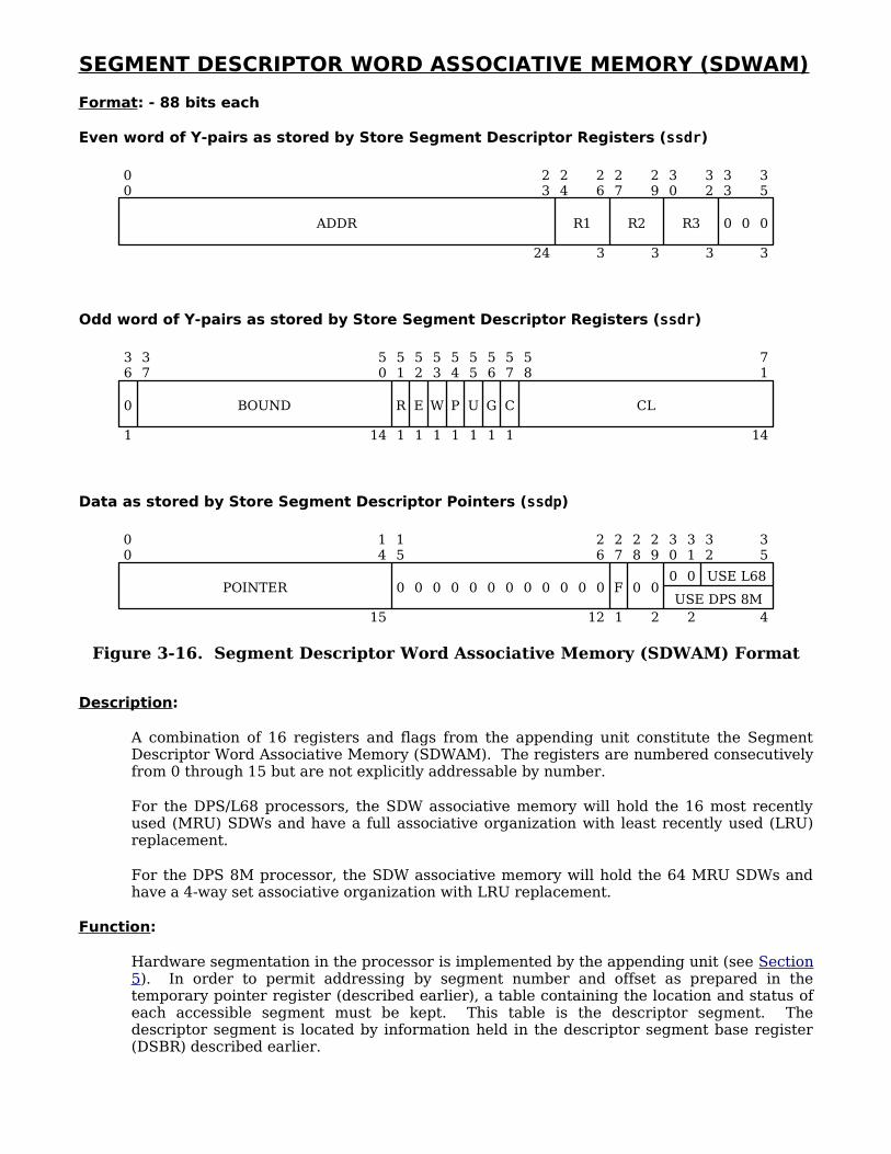
SEGMENT DESCRIPTOR WORD ASSOCIATIVE MEMORY (SDWAM)
Format: - 88 bits each
Even word of Y-pairs as stored by Store Segment Descriptor Registers (ssdr)
Odd word of Y-pairs as stored by Store Segment Descriptor Registers (ssdr)
Data as stored by Store Segment Descriptor Pointers (ssdp)
Figure 3-16. Segment Descriptor Word Associative Memory (SDWAM) Format
Description:
A combination of 16 registers and flags from the appending unit constitute the Segment Descriptor Word Associative Memory (SDWAM). The registers are numbered consecutively from 0 through 15 but are not explicitly addressable by number.
For the DPS/L68 processors, the SDW associative memory will hold the 16 most recently used (MRU) SDWs and have a full associative organization with least recently used (LRU) replacement.
For the DPS 8M processor, the SDW associative memory will hold the 64 MRU SDWs and have a 4-way set associative organization with LRU replacement.
Function:
Hardware segmentation in the processor is implemented by the appending unit (see Section 5). In order to permit addressing by segment number and offset as prepared in the temporary pointer register (described earlier), a table containing the location and status of each accessible segment must be kept. This table is the descriptor segment. The descriptor segment is located by information held in the descriptor segment base register (DSBR) described earlier.
00
23
ADDR
24
24
R1
26
3
27
R2
29
3
30
R3
32
3
33
0 0
35
0
3
36
0
1
37
50
BOUND
14
51
R
1
52
E
1
53
W
1
54
P
1
55
U
1
56
G
1
57
C
1
58
71
CL
14
00
14
POINTER
15
15
0 0 0 0 0 0 0 0 0 0 0
26
0
12
27
F
1
28
0
29
0
2
30
0
31
0
2
32
USE L68
35
4USE DPS 8M
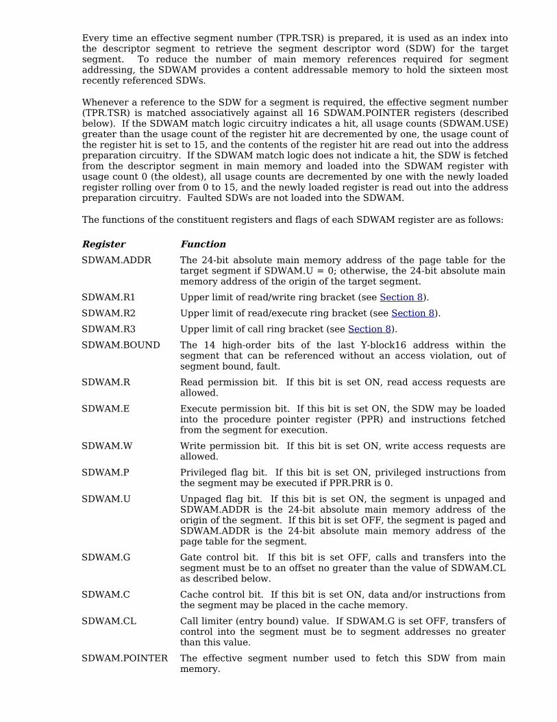
Every time an effective segment number (TPR.TSR) is prepared, it is used as an index into the descriptor segment to retrieve the segment descriptor word (SDW) for the target segment. To reduce the number of main memory references required for segment addressing, the SDWAM provides a content addressable memory to hold the sixteen most recently referenced SDWs.
Whenever a reference to the SDW for a segment is required, the effective segment number (TPR.TSR) is matched associatively against all 16 SDWAM.POINTER registers (described below). If the SDWAM match logic circuitry indicates a hit, all usage counts (SDWAM.USE) greater than the usage count of the register hit are decremented by one, the usage count of the register hit is set to 15, and the contents of the register hit are read out into the address preparation circuitry. If the SDWAM match logic does not indicate a hit, the SDW is fetched from the descriptor segment in main memory and loaded into the SDWAM register with usage count 0 (the oldest), all usage counts are decremented by one with the newly loaded register rolling over from 0 to 15, and the newly loaded register is read out into the address preparation circuitry. Faulted SDWs are not loaded into the SDWAM.
The functions of the constituent registers and flags of each SDWAM register are as follows:
Register Function
SDWAM.ADDR The 24-bit absolute main memory address of the page table for the target segment if SDWAM.U = 0; otherwise, the 24-bit absolute main memory address of the origin of the target segment.
SDWAM.R1 Upper limit of read/write ring bracket (see Section 8).
SDWAM.R2 Upper limit of read/execute ring bracket (see Section 8).
SDWAM.R3 Upper limit of call ring bracket (see Section 8).
SDWAM.BOUND The 14 high-order bits of the last Y-block16 address within the segment that can be referenced without an access violation, out of segment bound, fault.
SDWAM.R Read permission bit. If this bit is set ON, read access requests are allowed.
SDWAM.E Execute permission bit. If this bit is set ON, the SDW may be loaded into the procedure pointer register (PPR) and instructions fetched from the segment for execution.
SDWAM.W Write permission bit. If this bit is set ON, write access requests are allowed.
SDWAM.P Privileged flag bit. If this bit is set ON, privileged instructions from the segment may be executed if PPR.PRR is 0.
SDWAM.U Unpaged flag bit. If this bit is set ON, the segment is unpaged and SDWAM.ADDR is the 24-bit absolute main memory address of the origin of the segment. If this bit is set OFF, the segment is paged and SDWAM.ADDR is the 24-bit absolute main memory address of the page table for the segment.
SDWAM.G Gate control bit. If this bit is set OFF, calls and transfers into the segment must be to an offset no greater than the value of SDWAM.CL as described below.
SDWAM.C Cache control bit. If this bit is set ON, data and/or instructions from the segment may be placed in the cache memory.
SDWAM.CL Call limiter (entry bound) value. If SDWAM.G is set OFF, transfers of control into the segment must be to segment addresses no greater than this value.
SDWAM.POINTER The effective segment number used to fetch this SDW from main memory.
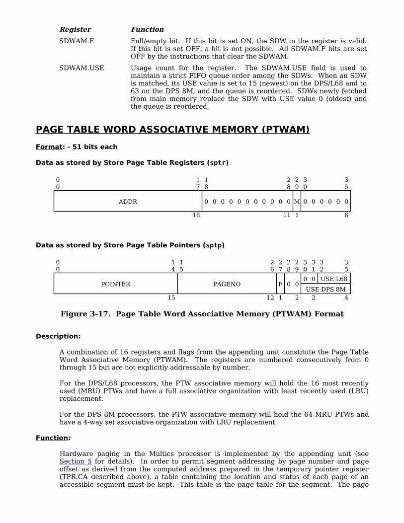
Register Function
SDWAM.F Full/empty bit. If this bit is set ON, the SDW in the register is valid. If this bit is set OFF, a hit is not possible. All SDWAM.F bits are set OFF by the instructions that clear the SDWAM.
SDWAM.USE Usage count for the register. The SDWAM.USE field is used to maintain a strict FIFO queue order among the SDWs. When an SDW is matched, its USE value is set to 15 (newest) on the DPS/L68 and to 63 on the DPS 8M, and the queue is reordered. SDWs newly fetched from main memory replace the SDW with USE value 0 (oldest) and the queue is reordered.
PAGE TABLE WORD ASSOCIATIVE MEMORY (PTWAM)
Format: - 51 bits each
Data as stored by Store Page Table Registers (sptr)
Data as stored by Store Page Table Pointers (sptp)
Figure 3-17. Page Table Word Associative Memory (PTWAM) Format
Description:
A combination of 16 registers and flags from the appending unit constitute the Page Table Word Associative Memory (PTWAM). The registers are numbered consecutively from 0 through 15 but are not explicitly addressable by number.
For the DPS/L68 processors, the PTW associative memory will hold the 16 most recently used (MRU) PTWs and have a full associative organization with least recently used (LRU) replacement.
For the DPS 8M processors, the PTW associative memory will hold the 64 MRU PTWs and have a 4-way set associative organization with LRU replacement.
Function:
Hardware paging in the Multics processor is implemented by the appending unit (see Section 5 for details). In order to permit segment addressing by page number and page offset as derived from the computed address prepared in the temporary pointer register (TPR.CA described above), a table containing the location and status of each page of an accessible segment must be kept. This table is the page table for the segment. The page
00
ADDR
17
18
18
0 0 0 0 0 0 0 0 0 0
28
0
11
29
M
1
30
0 0 0 0 0
35
0
6
00
14
POINTER
15
15
PAGENO
26
12
27
F
1
28
0
29
0
2
30
0
31
0
2
32
USE L68
35
4USE DPS 8M

table for an accessible paged segment is located by information held in the segment descriptor word (SDW) for the segment.
Every time a computed address (TPR.CA) for a paged segment is prepared, it is separated into a page number and a page offset. The page number is used as an index into the page table to retrieve the page table word (PTW) for the target page. To reduce the number of main memory references required for paging, the PTWAM provides a content addressable memory to hold the 16 most recently referenced PTWs.
Whenever a reference to the PTW for a page of a paged segment is required, the page number (as derived from TPR.CA) is matched associatively against all 16 PTWAM.PAGENO registers (described below) and, simultaneously, TPR.TSR is matched against PTWAM.POINTER (described below). If the PTWAM match logic circuitry indicates a hit, all usage counts (PTWAM.USE) greater than the usage count of the register hit are decremented by one, the usage count of the register hit is set to 15, and the contents of the register hit are read out into the address preparation circuitry. If the PTWAM match logic does not indicate a hit, the PTW is fetched from main memory and loaded into the PTWAM register with usage count 0 (the oldest), all usage counts are decremented by one with the newly loaded register rolling over from 0 to 15, and the newly loaded register is read out into the address preparation circuitry. Faulted PTWs are not loaded into the PTWAM.
The functions of the constituent registers and flags of each PTWAM register are: (See Section 8 for additional details.)
Register Function
PTWAM.ADDR The 18 high-order bits of the 24-bit absolute main memory address of the page. The hardware ignores low-order bits of this page address according to page size based on the following:
Page size in words64
128256512
102420484096
ADDR bits ignorednone17
16-1715-1714-1713-1712-17
PTWAM.M Page modified flag bit. This bit is set ON whenever the PTW is used for a store type instruction. When the bit changes value from 0 to 1, a special extra cycle is generated to write it back into the PTW in the page table in main memory.
PTWAM.POINTER The effective segment number used to fetch this PTW from main memory.
PTWAM.PAGENO The 12 high-order bits of the 18-bit computed address (TPR.CA) used to fetch this PTW from main memory. Low-order bits are forced to zero by the hardware and not used as part of the page table index according to page size based on the following:
Page size in words64
128256512
102420484096
PAGENO bits forcednone11
10-1109-1108-1107-1106-11
PTWAM.F Full/empty bit. If this bit is set ON, the PTW in the register is valid. If this bit is set OFF, a hit is not possible. All PTWAM.F bits are set OFF by the instructions that clear the PTWAM.
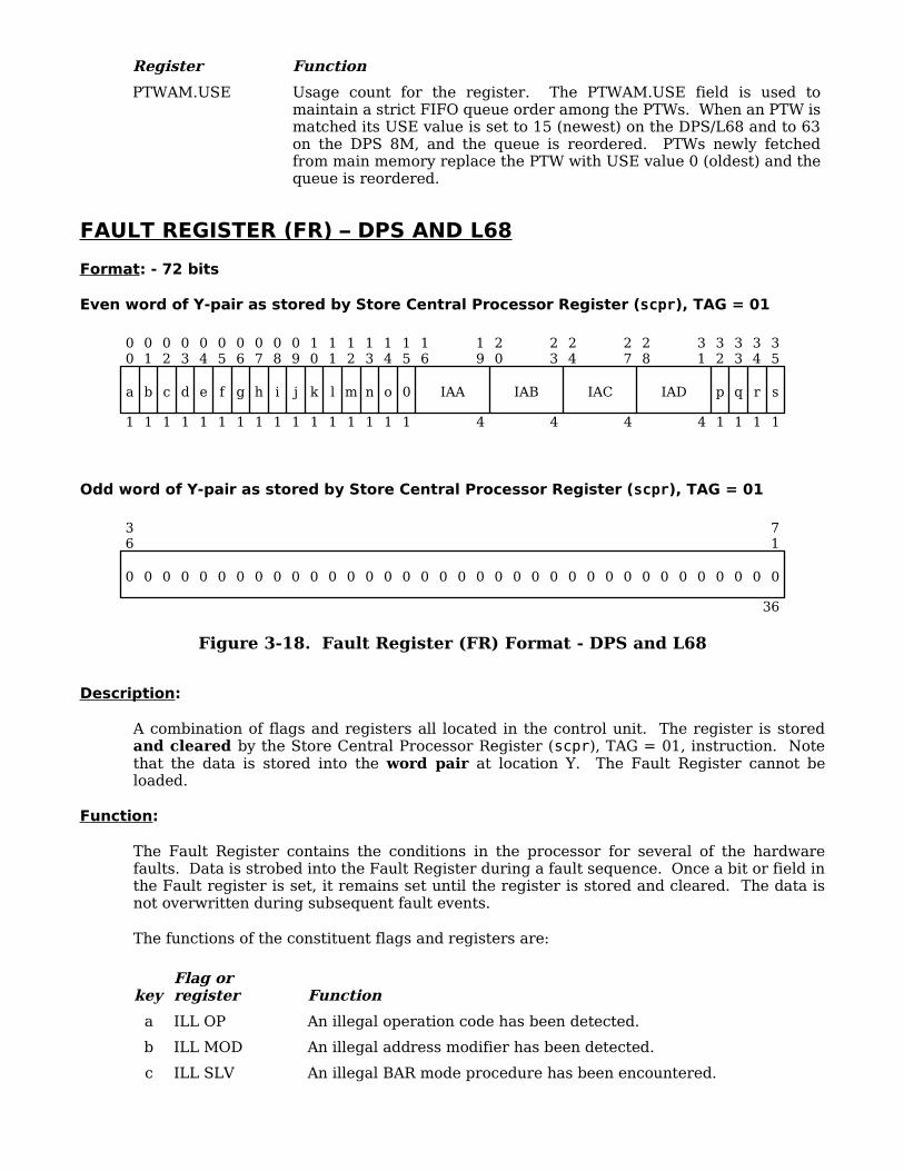
Register Function
PTWAM.USE Usage count for the register. The PTWAM.USE field is used to maintain a strict FIFO queue order among the PTWs. When an PTW is matched its USE value is set to 15 (newest) on the DPS/L68 and to 63 on the DPS 8M, and the queue is reordered. PTWs newly fetched from main memory replace the PTW with USE value 0 (oldest) and the queue is reordered.
FAULT REGISTER (FR) – DPS AND L68
Format: - 72 bits
Even word of Y-pair as stored by Store Central Processor Register (scpr), TAG = 01
Odd word of Y-pair as stored by Store Central Processor Register (scpr), TAG = 01
Figure 3-18. Fault Register (FR) Format - DPS and L68
Description:
A combination of flags and registers all located in the control unit. The register is stored and cleared by the Store Central Processor Register (scpr), TAG = 01, instruction. Note that the data is stored into the word pair at location Y. The Fault Register cannot be loaded.
Function:
The Fault Register contains the conditions in the processor for several of the hardware faults. Data is strobed into the Fault Register during a fault sequence. Once a bit or field in the Fault register is set, it remains set until the register is stored and cleared. The data is not overwritten during subsequent fault events.
The functions of the constituent flags and registers are:
keyFlag or register Function
a ILL OP An illegal operation code has been detected.
b ILL MOD An illegal address modifier has been detected.
c ILL SLV An illegal BAR mode procedure has been encountered.
00
a
1
01
b
1
02
c
1
03
d
1
04
e
1
05
f
1
06
g
1
07
h
1
08
i
1
09
j
1
10
k
1
11
l
1
12
m
1
13
n
1
14
o
1
15
0
1
16
IAA
19
4
20
23
4
24
27
4
28
31
4
32
p
1
33
q
1
34
r
1
35
s
1
IAB IAC IAD
36
0 0 0 0 0 0 0 0 0 0 0 0 0 0 0 0 0 0 0 0 0 0 0 0 0 0 0 0 0 0 0 0 0 0 0
71
0
36

keyFlag or register Function
d ILL PROC An illegal procedure other than the three above has been encountered.
e NEM A nonexistent main memory address has been requested.
f OOB A BAR mode boundary violation has occurred.
g ILL DIG An illegal decimal digit or sign has been detected by the decimal unit.
h PROC PARU A parity error has been detected in the upper 36 bits of data.
i PROC PARL A parity error has been detected in the lower 36 bits of data.
j $CON A A $CONNECT signal has been received through port A.
k $CON B A $CONNECT signal has been received through port B.
1 $CON C A $CONNECT signal has been received through port C.
m $CON D A $CONNECT signal has been received through port D.
n DA ERR1 Operation not complete. Processor/system controller interface sequence error 1 has been detected. ($DATA-AVAIL received with no prior $INTERRUPT sent.)
o DA ERR2 Operation not complete. Processor/system controller interface sequence error 2 has been detected. (Multiple $DATA-AVAIL received or $DATA-AVAIL received out of order.)
IAA Coded illegal action, port A. (see Table 3-2)
IAB Coded illegal action, port B. (See Table 3-2)
IAC Coded illegal action, port C. (See Table 3-2)
IAD Coded illegal action, port D. (See Table 3-2)
p CPAR DIR A parity error has been detected in the cache memory directory.
q CPAR STR A data parity error has been detected in the cache memory.
r CPAR IA An illegal action has been received from a system controller during a store operation with cache memory enabled. This implies that the data are correct in cache memory and incorrect in main memory.
s CPAR BLK A cache memory parity error has occurred during a cache memory data block load.
Table 3-2. System Controller Illegal Action Codes
Code Priority Fault Reason
00 -- No illegal action
01 -- Command Unassigned
02 05 Store Nonexistent address
03 01 Command Stop on condition
04 -- Command Unassigned
05 12 Parity Data parity, store unit to system controller
06 11 Parity Data parity in store unit
07 10 Parity Data parity in store unit and store unit to system controller
10 04 Command Not control (a)

Code Priority Fault Reason
11 13 Command Port not enabled
12 03 Command Illegal command
13 07 Store Store unit not ready
14 02 Parity Zone-address-command parity, processor to system controller
15 06 Parity Data parity, processor to system controller
16 08 Parity Zone-address-command parity, system controller to store unit
17 09 Parity Data parity, system controller to store unit
(a) This illegal action code not relevant to later model system controllers.
FAULT REGISTER (FR) - DPS 8M
Format: - 72 bits
Even word of Y-pair as stored by Store Central Processor Register (scpr), TAG = 01
Odd word of Y-pair as stored by Store Central Processor Register (scpr), TAG = 01
Figure 3-19. Fault Register (FR) Format - DPS 8M
Function:
The Fault Register contains the conditions in the processor for several of the hardware faults on the DPS 8M CPU and cache directory buffer overflows. Data is strobed into the Fault Register during a fault or buffer overflow fault sequence. Once a bit or field in the Fault Register is set, it remains set until the register is stored and cleared. The data is not overwritten during subsequent fault events.
The functions of the constituent flags and registers are:
keyFlag or register Fault Function
a ILL OP IPR An illegal operation code has been detected.
b ILL MOD IPR An illegal address modifier has been detected.
c ILL SLV IPR An illegal BAR mode procedure has been encountered.
00
a
1
01
b
1
02
c
1
03
d
1
04
e
1
05
f
1
06
g
1
07
h
1
08
i
1
09
j
1
10
k
1
11
l
1
12
m
1
13
n
1
14
o
1
15
0
1
16
IAA
19
4
20
23
4
24
27
4
28
31
4
32
p
1
33
q
1
34
r
1
35
s
1
IAB IAC IAD
36
t
1
37
u
1
38
v
1
39
w
1
40
x
1
41
y
1
42
z
1
43
A
1
44
B
1
45
C
1
46
D
1
47
E
1
48
F
1
0 0 0 0 0 0 0 0 0 0 0 0 0 0 0 0 0 0 0 0 0 0
71
0
25

keyFlag or register Fault Function
d ILL PROC IPR An illegal procedure other than the three above has been encountered.
e NEM ONC A nonexistent main memory address has been requested.
f OOB STR A BAR mode boundary violation has occurred.
g ILL DIG IPR An illegal decimal digit or sign has been detected by the decimal unit.
h PROC PARU PAR A parity error has been detected in the upper 36 bits of data.
i PROC PARL PAR A parity error has been detected in the lower 36 bits of data.
j $CON A CON A $CONNECT signal has been received through port A.
k $CON B CON A $CONNECT signal has been received through port B.
l $CON C CON A $CONNECT signal has been received through port C.
m $CON D CON A $CONNECT signal has been received through port D.
n DA ERR ONC Operation not complete. Processor/system controller interface sequence error 1 has been detected. ($DATA-AVAIL received with no prior $INTERRUPT sent.)
o DA ERR2 ONC Operation not completed. Processor/system controller interface sequence error 2 has been detected. (Multiple $DATA-AVAIL received or $DATA-AVAIL received out of order.)
IAA Coded illegal action, port A. (See Table 3-2)
IAB Coded illegal action, port B. (See Table 3-2)
IAC Coded illegal action, port C. (See Table 3-2)
IAD Coded illegal action, port D. (See Table 3-2)
p CPAR DIR None A parity error has been detected in the cache memory directory.
q CPAR STR PAR A data parity error has been detected in the cache memory.
r CPAR IA PAR An illegal action has been received from a system controller during a store operation with cache memory enabled. This implies that the data are correct in cache memory and incorrect in main memory.
s CPAR BLK PAR A cache memory parity error has occurred during a cache memory data block load.
Cache Duplicate Directory WNO Buffer Overflow
t None Port A
u None Port B
v None Port C
w None Port D
x None Cache Primary Directory WNO Buffer Overflow
y None Write Notify (WNO) Parity Error on Port A, B, C, or D.
None Cache Duplicate Directory Parity Error
z None Level 0
A None Level 1
B None Level 2

keyFlag or register Fault Function
C None Level 3
D Cache Duplicate Directory Multiple Match
E None A parity error has been detected in the SDWAM.
F None A parity error has been detected in the PTWAM.
MODE REGISTER (MR) - DPS AND L68
Format: - 33 bits
Even word of Y-pair as stored by Store Central Processor Register (scpr), TAG = 06
Figure 3-20. Mode Register (MR) Format - DPS and L68
Description:
An assemblage of flags and registers from the control unit. The Mode Register and the Cache Mode Register are both stored into the Y-pair by the Store Central Processor Register (scpr), TAG = 06. The Mode Register is loaded with the Load Central Processor Register (lcpr), TAG = 04, instruction.
Function:
The Mode Register controls the operation of those features of the processor that are capable of being enabled and disabled.
The functions of the constituent flags and registers are:
keyFlag or register Function
FFV A floating-fault vector address. The 15 high-order bits of the Y-block8 address of four word pairs constituting a floating-fault vector. Traps to these floating faults are generated by other conditions the mode register sets.
a OC TRAP Trap on OPCODE match. If this bit is set ON and OPCODE matches the operation code of the instruction for which an address is being prepared (including indirect cycles), generate the second floating fault (xed FFV+2). See NOTE below.
b ADR TRAP Trap on ADDRESS match. If this bit is set ON and the computed address (TPR.CA) matches the setting of the address switches on the processor maintenance panel, generate the fourth floating fault (xed FFV+6). See NOTE below.
00
14
FFV
15
15
0
1
16
a
1
17
b
1
18
c1
19
d1
20
e1
21
f1
22
g
23
2
24
h
25
2
26
0
27
02
28
i
1
29
j
1
30
k
1
31
l
1
32
m
1
33
0
34
0
2
35
n
1
OPCODE
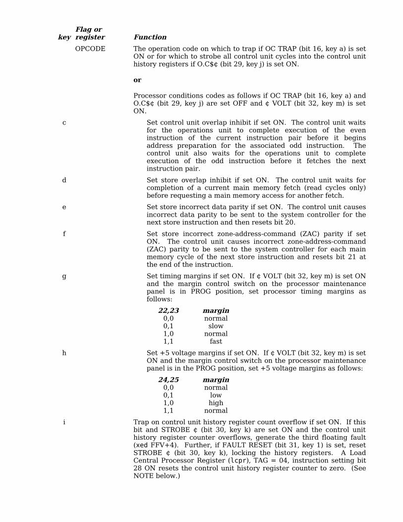
keyFlag or register Function
OPCODE The operation code on which to trap if OC TRAP (bit 16, key a) is set ON or for which to strobe all control unit cycles into the control unit history registers if O.C$¢ (bit 29, key j) is set ON.
or
Processor conditions codes as follows if OC TRAP (bit 16, key a) and O.C$¢ (bit 29, key j) are set OFF and ¢ VOLT (bit 32, key m) is set ON.
c Set control unit overlap inhibit if set ON. The control unit waits for the operations unit to complete execution of the even instruction of the current instruction pair before it begins address preparation for the associated odd instruction. The control unit also waits for the operations unit to complete execution of the odd instruction before it fetches the next instruction pair.
d Set store overlap inhibit if set ON. The control unit waits for completion of a current main memory fetch (read cycles only) before requesting a main memory access for another fetch.
e Set store incorrect data parity if set ON. The control unit causes incorrect data parity to be sent to the system controller for the next store instruction and then resets bit 20.
f Set store incorrect zone-address-command (ZAC) parity if set ON. The control unit causes incorrect zone-address-command (ZAC) parity to be sent to the system controller for each main memory cycle of the next store instruction and resets bit 21 at the end of the instruction.
g Set timing margins if set ON. If ¢ VOLT (bit 32, key m) is set ON and the margin control switch on the processor maintenance panel is in PROG position, set processor timing margins as follows:
22,230,00,11,01,1
marginnormal
slownormal
fast
h Set +5 voltage margins if set ON. If ¢ VOLT (bit 32, key m) is set ON and the margin control switch on the processor maintenance panel is in the PROG position, set +5 voltage margins as follows:
24,250,00,11,01,1
marginnormal
lowhigh
normal
i Trap on control unit history register count overflow if set ON. If this bit and STROBE ¢ (bit 30, key k) are set ON and the control unit history register counter overflows, generate the third floating fault (xed FFV+4). Further, if FAULT RESET (bit 31, key 1) is set, reset STROBE ¢ (bit 30, key k), locking the history registers. A Load Central Processor Register (lcpr), TAG = 04, instruction setting bit 28 ON resets the control unit history register counter to zero. (See NOTE below.)

keyFlag or register Function
j O.C$¢ Strobe control unit history registers on OPCODE match. If this bit and STROBE ¢ (bit 30, key k) are set ON and the operation code of the current instruction matches OPCODE, strobe the control unit history registers on all control unit cycles (including indirect cycles).
k STROBE ¢ Enable history registers. If this bit is set ON, all history registers are strobed at appropriate points in the various processor cycles. If this bit is set OFF or MR ENABLE (bit 35, key n) is set OFF, all history registers are locked. This bit is set OFF with a Load Central Processor Register (lcpr), TAG = 04, instruction providing a 0 bit, by an operation not complete fault, and, conditionally, by other faults (see FAULT RESET (bit 31, key 1) below). Once set OFF, this bit must be set ON with a Load Central Processor Register (lcpr), TAG = 04, instruction providing a 1 bit to re-enable the history registers.
l FAULT RESET History register lock control. If this bit is set ON, set STROBE ¢ (bit 30, key k) OFF, locking the history registers for all faults including the floating faults. See NOTE below.
m ¢ VOLT Test mode indicator. This bit is set ON whenever the TEST/NORMAL switch on the processor maintenance panel is in TEST position; otherwise, it is set OFF. It serves to enable the program control of voltage and timing margins.
n MR ENABLE Enable mode register. When this bit is set ON, all other bits and controls of the mode register are active. When this bit is set OFF, the mode register controls are disabled.
NOTE: The traps described above (address match, OPCODE match, control unit history register counter overflow) occur after completion of the next odd instruction following their detection. They are handled as Group 7 faults in regard to servicing and inhibition. (See Section 7 for descriptions of these faults.) The complete Group 7 priority sequence (in increasing order) is:
1 - Connect
2 - Time runout
3 - Shutdown
4 - OPCODE trap
5 - Control unit history register counter overflow
6 - Address match trap
7 - External interrupts

MODE REGISTER (MR) - DPS 8M
Format: - 36 bits
Even word of Y-pair as stored by Store Central Processor Register (scpr), TAG = 06
Figure 3-21. Mode Register (MR) Format - DPS 8M
Description:
An assemblage of flags and registers from the control unit. The Mode Register and the Cache Mode Register are both stored into the Y-pair by the Store Central Processor Register (scpr), TAG = 06. The Mode Register is loaded with the Load Central Processor Register (lcpr), TAG = 04, instruction.
Function:
The mode register controls the operation of those features of the processor that are capable of being enabled and disabled.
The functions of the constituent flags and registers are:
keyFlag or register Function
a cuolin Set CU overlap inhibit. The CU waits for the OU to complete execution of the even instruction before it begins address preparation for the associated odd instruction. The CU also waits for the OU to complete execution of the odd instruction before it fetches the next instruction pair.
b solin Set store overlap inhibit. The CU waits for completion of a current memory fetch (read cycles only) before requesting a memory access for another fetch.
c sdpap Set store incorrect data parity. The CU causes incorrect data parity to be sent to the SC for the next data store instruction and then resets bit 20.
d separ Set store incorrect ZAC parity. The CU causes incorrect zone-address-command (ZAC) parity to be sent to the SC for each memory cycle of the next data store instruction and resets bit 21 at the end of the instruction.
e tm Set timing margins. If bit 32 key (k) is set and the margin control switch on the CPU maintenance panel is in program position, set CPU timing margins as follows:
22,230,00,11,01,1
marginnormal
slownormal
fast
f vm Set +5 voltage margins. If bit 32 (key k) is set and the margin control switch on the CPU maintenance panel is in the program position, set +5 voltage margins as follows:
00
0 0 0 0 0 0 0 0 0 0 0 0 0 0 0 0 0
17
0
18
18
a
1
19
b
1
20
c
1
21
d
1
22
e
23
2
24
f
25
2
26
0
27
0
2
28
g
1
29
h
1
30
i
1
31
j
1
32
k
1
33
l
1
34
0
1
35
m
1

keyFlag or register Function
24,250,00,11,01,1
marginnormal
lowhigh
normal
g hrhlt Stop HR Strobe on HR Counter Overflow. (Setting bit 28 shall cause the HR counter to be reset to zero.)
h hrxfr Strobe the HR on Transfer Made. If bits 29,30, and 35 are = 1, the HR will be strobed on all Transfers Made. Bits 36-53 of the OU/DU register will indicate the "From" location and bits 36-59 of the CU register will contain the real address of the final "To" location.
i ihr Enable History Registers. If bit 30 = 1, the HRs may be strobed. If bit 30 = 0 or bit 35 = 0, they will be locked out. This bit will be reset by either an LCPR with the bit corresponding to 30 = 0 or by an Op Not Complete fault. It may be reset by other faults (see bit 31). After being reset, it must be enabled by another LCPR instruction before the History Registers may be strobed again.
j ihrrs Additional resetting of bit 30. If bit 31 = 1, the following faults also reset bit 30:
- Lock Up- Parity- Command- Store- Illegal Procedure- Shutdown
k mrgctl Margin Control. Bit 32 informs the software when it can control margins. A one indicates that software has control. When the LOCAL/REMOTE switch on the power supply is in REMOTE and bit 35 = 1, bit 32 is set to 1 by occurrence of the following conditions: the NORMAL/TEST switch is in the TEST position, the Memory and CU Overlap Inhibit switches are OFF, the Timing Margins for the OU, CU, DU and VU are NORMAL, and the Forced Data and ZAC Parity are OFF.
l hexfp Hexadecimal Exponent Floating Point Arithmetic Mode can be set. When this bit is set, the Hex mode becomes effective when the Indicator Register bit 32 is set to 1.
m emr Enable Mode Register. Unless bit 35 = 1, all other bits in the Mode Register are ignored and the History Register is ignored and locked.
CACHE MODE REGISTER (CMR) - DPS AND L68
Format: - 28 bits
Odd word of Y-pair as stored by Store Central Processor Register (scpr), TAG = 06
Figure 3-22. Cache Mode Register (CMR) Format - DPS and L68
36
50
CACHE DIR ADDRESS
1
51
a
1
52
b
1
53
0
1
54
c
1
55
d
1
56
e
1
57
f
1
58
0
1
59
g
1
60
h
1
61
i
1
62
j
63
2
64
0 0 0 0 0
69
0
6
70
k
71
2

Description:
An assemblage of flags and registers from the control unit. The Mode Register and Cache Mode Register are both stored into the Y-pair by the Store Central Processor Register (scpr), TAG = 06, instruction. The Cache Mode Register is loaded with the Load Central Processor Register (lcpr), TAG = 02, instruction.
The data stored from the cache mode register is address-dependent. The algorithm used to map main memory into the cache memory (see Section 9) is effective for the Store Central Processor Register (scpr) instruction. In general, the user may read out data from the directory entry for any cache memory block by proper selection of certain subfields in the 24-bit absolute main memory address. In particular, the user may read out the directory entry for the cache memory block involved in a suspected cache memory error by ensuring that the required 24-bit absolute main memory address subfields are the same as those for the access which produced the suspected error.
The fault handling procedure(s) should be unencacheable (SDW.C = 0) and the history registers and cache memory should be disabled as quickly as possible in order that vital information concerning the suspected error not be lost.
Function:
The Cache Mode register provides configuration information and software control over the operation of the cache memory. Those items with an "x" in the column headed L are not loaded by the Load Central Processor Register (lcpr), TAG = 02, instruction.
The functions of the constituent flags and registers are:
key L Register Function
x CACHE DIR ADDRESS
15 high-order bits of the cache memory block address from the cache directory.
a x PAR BIT Cache memory directory parity bit.
b x LEV FUL The selected column and level is loaded with active data.
c CSH1 ON Enable the upper 1024 words of the cache memory (see Section 9).
d CSH2 ON Enable the lower 1024 words of the cache memory (see Section 9).
e OPND ON Enable the cache memory for operands (see Section 9).
f INST ON Enable the cache memory for instructions (see Section 9).
g CSH REG Enable cache-to-register (dump) mode. When this bit is set ON, double-precision operations unit read operands (e.g., Load AQ (ldaq) operands) are read from the cache memory according to the mapping algorithm and without regard to matching of the full 24-bit absolute main memory address. All other operands address main memory as though the cache memory were disabled. This bit is reset automatically by the hardware for any fault or interrupt.
h x STR ASD Enable store aside. When this bit is set ON, the processor does not wait for main memory cycle completion after a store operation but proceeds after the cache memory cycle is complete.
i x COL FUL Selected cache memory column is full.
j x RRO A,B Cache round robin counter (see Section 9).
k LUF MSB,LSB Lockup timer setting. The lockup timer may be set to four different values according to the value of this field.

LUF value
0123
Lockup time
2ms4ms8ms16ms
The lockup timer is set to 16ms when the processor is initialized.
CACHE MODE REGISTER (CMR) - DPS 8M
Format: - 36 bits
Odd word of Y-pair as stored by Store Central Processor Register (scpr), TAG = 06.
Figure 3-23. Cache Mode Register (CMR) Format - DPS 8M
Description:
An assemblage of flags and registers from the control unit. The Mode Register and Cache Mode Register are both stored into the Y-pair by the Store Central Processor Register (scpr), TAG = 06, instruction. The Cache Mode Register is loaded with the Load Central Processor Register (lcpr), TAG = 02, instruction.
The data stored from the Cache Mode register is address-dependent. The algorithm used to map main memory into the cache memory (see Section 9) is effective for the Store central Processor Register (scpr) instruction. In general, the user may read out data from the directory entry for any cache memory block by proper selection of certain subfields in the 24-bit absolute main memory address. In particular, the user may read out the directory entry for the cache memory block involved in a suspected cache memory error by ensuring that the required 24-bit absolute main memory address subfields are the same as those for the access which produced the suspected error.
The fault handling procedure(s) should be unencacheable (SDW.D = 0) and the history registers and cache memory should be disabled as quickly as possible in order that vital information concerning the suspected error not be lost.
Function:
The Cache Mode Register provides configuration information and software control over the operation of the cache memory. Those items with an "x" in the column headed L are not loaded by the Load Central Processor Register (lcpr), TAG = 02, instruction.
The functions of the constituent flags and registers are:
key L Register Function
x CACHE DIR ADDRESS
15 high-order bits of the cache memory block address from the cache directory.
a x PAR BIT Cache memory directory parity bit.
b x LEV FUL The selected column and level is loaded with active data.
36
50
CACHE DIR ADDRESS
15
51
a
1
52
b
1
53
0
1
54
c
1
55
d
1
56
0
1
57
e
1
58
0
1
59
f
1
60
g
1
61
h
1
62
i
63
2
64
0 0 0
67
0
4
68
j
1
69
0
1
70
k
71
2
key L Register Function
c CSH1 ON Enable the upper 4096 words of the cache memory (see Section 9).
d CSH2 ON Enable the lower 4096 words of the cache memory (see Section 9).
e INST ON Enable the cache memory for instructions (see Section 9).
f CSH REG Enable cache-to-register (dump) mode. When this bit is set ON, double-precision operations unit read operands (e.g., Load AQ (ldaq) operands) are read from the cache memory according to the mapping algorithm and without regard to matching of the full 24-bit absolute main memory address. All other operands address main memory as though the cache memory were disabled. This bit is reset automatically by the hardware for any fault or interrupt.
g x STR ASD Enable store aside. When this bit is set ON, the processor does not wait for main memory cycle completion after a store operation but proceeds after the cache memory cycle is complete.
h x COL FUL Selected cache memory column is full.
i x RRO A,B Cache round-robin counter (see Section 9).
j Bypass cache bit. Enables the bypass option of SDW.C when set OFF. See Notes below for further information.
k LUF MSB,LSB Lockup timer setting. The lockup timer may be set to four different values according to the value of this field.
LUF value
0123
Lockup time
2ms4ms8ms16ms
The lockup timer is set to 16ms when the processor is initialized.
Notes
1. The COL FUL, RRO A, RRO B, and CACHE DIR ADDRESS fields reflect different locations in cache depending on the final (absolute) address of the scpr instruction storing this data.
2. If either cache enable bit c or d changes from disable state to enable state, the entire cache is cleared.
3. The DPS 8M processors contain an 8k hardware-controlled cache memory. When running a mixed configuration of DPS 8M and DPS/L68 processors, bit 68 of the CMR (reference j) allows the DPS 8M processor to utilize software compatible with the older 2k software controlled by the DPS/L68 and DPS processors. The following summarizes the operation of the DPS 8M hardware-controlled cache.
a. The cache bypass option in the segment descriptor word is retained. An overriding bypass enable, bit 68 of the Cache Mode Register, is added. The cache mode is set as follows:
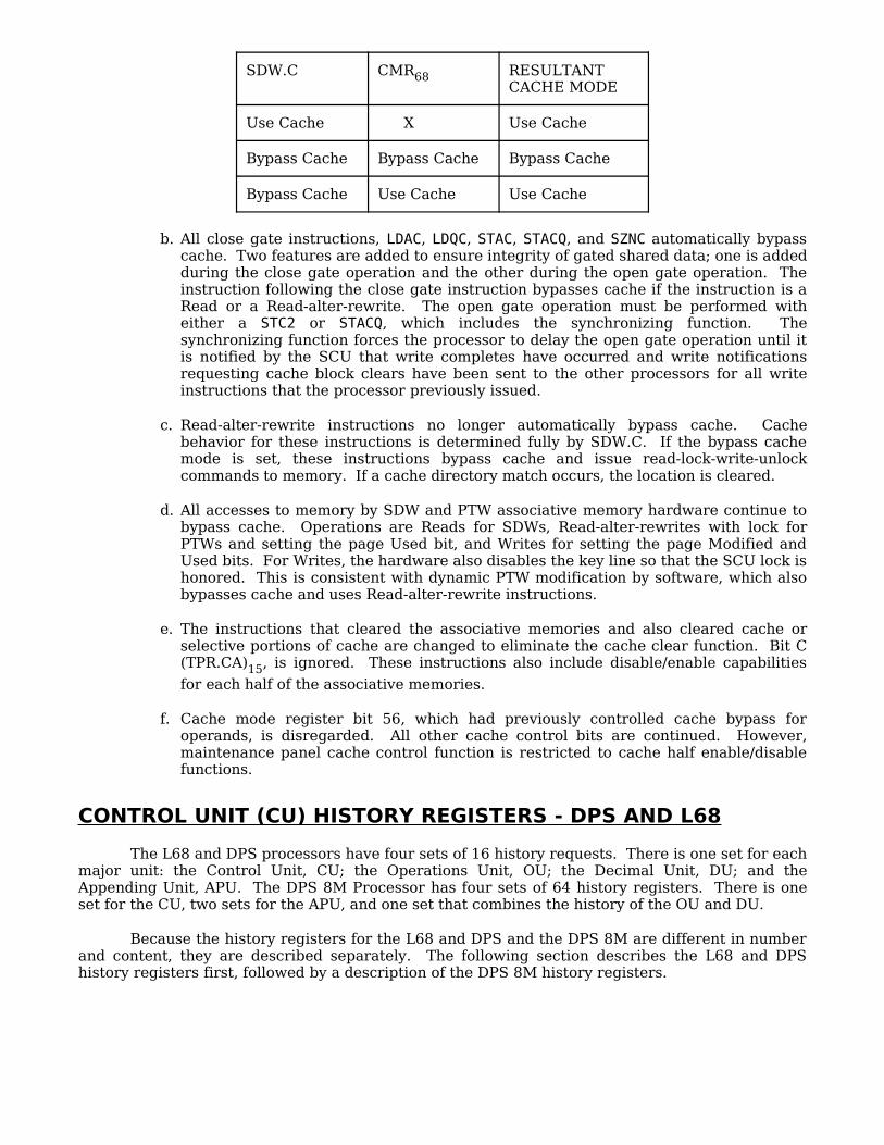
SDW.C CMR68 RESULTANT CACHE MODE
Use Cache X Use Cache
Bypass Cache Bypass Cache Bypass Cache
Bypass Cache Use Cache Use Cache
b. All close gate instructions, LDAC, LDQC, STAC, STACQ, and SZNC automatically bypass cache. Two features are added to ensure integrity of gated shared data; one is added during the close gate operation and the other during the open gate operation. The instruction following the close gate instruction bypasses cache if the instruction is a Read or a Read-alter-rewrite. The open gate operation must be performed with either a STC2 or STACQ, which includes the synchronizing function. The synchronizing function forces the processor to delay the open gate operation until it is notified by the SCU that write completes have occurred and write notifications requesting cache block clears have been sent to the other processors for all write instructions that the processor previously issued.
c. Read-alter-rewrite instructions no longer automatically bypass cache. Cache behavior for these instructions is determined fully by SDW.C. If the bypass cache mode is set, these instructions bypass cache and issue read-lock-write-unlock commands to memory. If a cache directory match occurs, the location is cleared.
d. All accesses to memory by SDW and PTW associative memory hardware continue to bypass cache. Operations are Reads for SDWs, Read-alter-rewrites with lock for PTWs and setting the page Used bit, and Writes for setting the page Modified and Used bits. For Writes, the hardware also disables the key line so that the SCU lock is honored. This is consistent with dynamic PTW modification by software, which also bypasses cache and uses Read-alter-rewrite instructions.
e. The instructions that cleared the associative memories and also cleared cache or selective portions of cache are changed to eliminate the cache clear function. Bit C (TPR.CA)15, is ignored. These instructions also include disable/enable capabilities
for each half of the associative memories.
f. Cache mode register bit 56, which had previously controlled cache bypass for operands, is disregarded. All other cache control bits are continued. However, maintenance panel cache control function is restricted to cache half enable/disable functions.
CONTROL UNIT (CU) HISTORY REGISTERS - DPS AND L68
The L68 and DPS processors have four sets of 16 history requests. There is one set for each major unit: the Control Unit, CU; the Operations Unit, OU; the Decimal Unit, DU; and the Appending Unit, APU. The DPS 8M Processor has four sets of 64 history registers. There is one set for the CU, two sets for the APU, and one set that combines the history of the OU and DU.
Because the history registers for the L68 and DPS and the DPS 8M are different in number and content, they are described separately. The following section describes the L68 and DPS history registers first, followed by a description of the DPS 8M history registers.
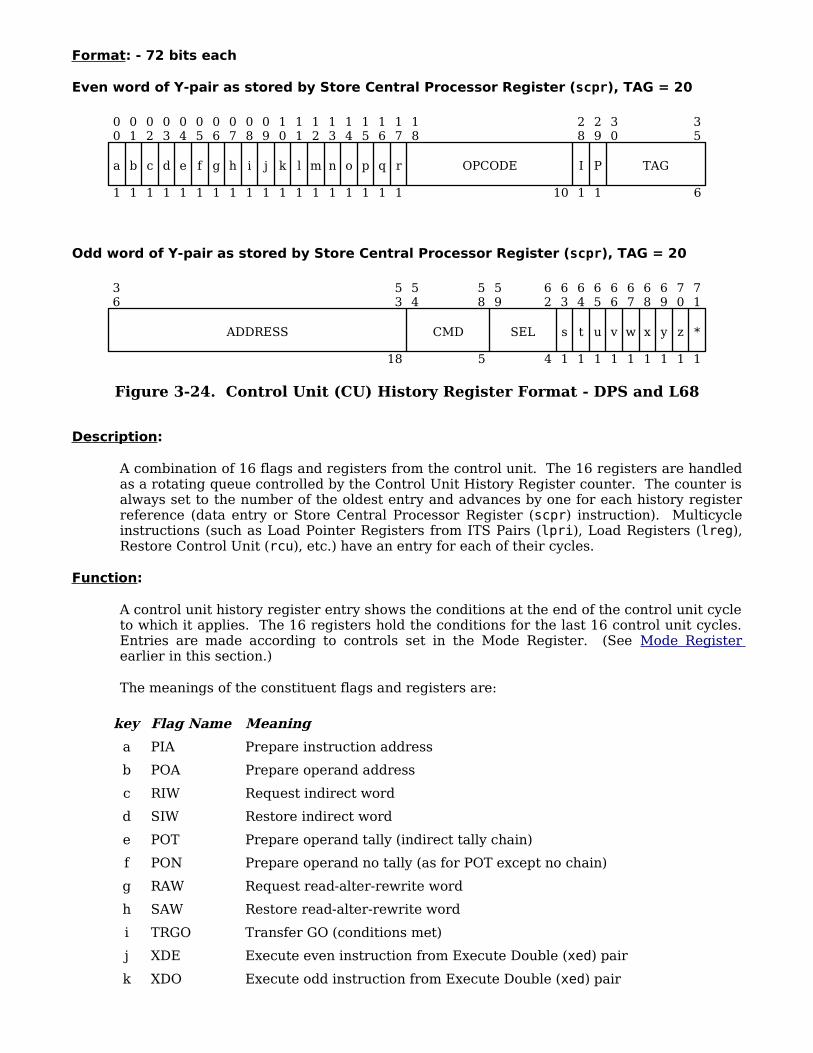
Format: - 72 bits each
Even word of Y-pair as stored by Store Central Processor Register (scpr), TAG = 20
Odd word of Y-pair as stored by Store Central Processor Register (scpr), TAG = 20
Figure 3-24. Control Unit (CU) History Register Format - DPS and L68
Description:
A combination of 16 flags and registers from the control unit. The 16 registers are handled as a rotating queue controlled by the Control Unit History Register counter. The counter is always set to the number of the oldest entry and advances by one for each history register reference (data entry or Store Central Processor Register (scpr) instruction). Multicycle instructions (such as Load Pointer Registers from ITS Pairs (lpri), Load Registers (lreg), Restore Control Unit (rcu), etc.) have an entry for each of their cycles.
Function:
A control unit history register entry shows the conditions at the end of the control unit cycle to which it applies. The 16 registers hold the conditions for the last 16 control unit cycles. Entries are made according to controls set in the Mode Register. (See Mode Register earlier in this section.)
The meanings of the constituent flags and registers are:
key Flag Name Meaning
a PIA Prepare instruction address
b POA Prepare operand address
c RIW Request indirect word
d SIW Restore indirect word
e POT Prepare operand tally (indirect tally chain)
f PON Prepare operand no tally (as for POT except no chain)
g RAW Request read-alter-rewrite word
h SAW Restore read-alter-rewrite word
i TRGO Transfer GO (conditions met)
j XDE Execute even instruction from Execute Double (xed) pair
k XDO Execute odd instruction from Execute Double (xed) pair
00
a
1
01
b
1
02
c
1
03
d
1
04
e
1
05
f
1
06
g
1
07
h
1
08
i
1
09
j
1
10
k
1
11
l
1
12
m
1
13
n
1
14
o
1
15
p
1
16
q
1
17
r
1
18
28
OPCODE
1
29
P
1
30
35
TAG
6
I
10
36
53
ADDRESS
18
54
58
CMD
5
59
62
SEL
4
63
s
1
64
t
1
65
u
1
66
v
1
67
w
1
68
x
1
69
y
1
70
z
1
71
*
1
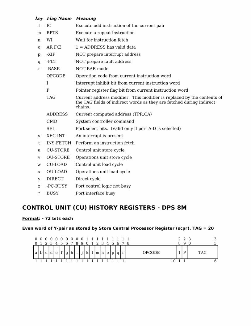
key Flag Name Meaning
l IC Execute odd instruction of the current pair
m RPTS Execute a repeat instruction
n WI Wait for instruction fetch
o AR F/E 1 = ADDRESS has valid data
p -XIP NOT prepare interrupt address
q -FLT NOT prepare fault address
r -BASE NOT BAR mode
OPCODE Operation code from current instruction word
I Interrupt inhibit bit from current instruction word
P Pointer register flag bit from current instruction word
TAG Current address modifier. This modifier is replaced by the contents of the TAG fields of indirect words as they are fetched during indirect chains.
ADDRESS Current computed address (TPR.CA)
CMD System controller command
SEL Port select bits. (Valid only if port A-D is selected)
s XEC-INT An interrupt is present
t INS-FETCH Perform an instruction fetch
u CU-STORE Control unit store cycle
v OU-STORE Operations unit store cycle
w CU-LOAD Control unit load cycle
x OU-LOAD Operations unit load cycle
y DIRECT Direct cycle
z -PC-BUSY Port control logic not busy
* BUSY Port interface busy
CONTROL UNIT (CU) HISTORY REGISTERS - DPS 8M
Format: - 72 bits each
Even word of Y-pair as stored by Store Central Processor Register (scpr), TAG = 20
00
a
1
01
b
1
02
c
1
03
d
1
04
e
1
05
f
1
06
g
1
07
h
1
08
i
1
09
j
1
10
k
1
11
l
1
12
m
1
13
n
1
14
o
1
15
p
1
16
q
1
17
r
1
18
28
OPCODE
1
29
P
1
30
35
TAG
6
I
10
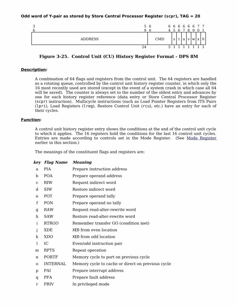
Odd word of Y-pair as stored by Store Central Processor Register (scpr), TAG = 20
Figure 3-25. Control Unit (CU) History Register Format - DPS 8M
Description:
A combination of 64 flags and registers from the control unit. The 64 registers are handled as a rotating queue, controlled by the control unit history register counter, in which only the 16 most recently used are stored (except in the event of a system crash in which case all 64 will be saved). The counter is always set to the number of the oldest entry and advances by one for each history register reference (data entry or Store Central Processor Register (scpr) instruction). Multicycle instructions (such as Load Pointer Registers from ITS Pairs (lpri), Load Registers (lreg), Restore Control Unit (rcu), etc.) have an entry for each of their cycles.
Function:
A control unit history register entry shows the conditions at the end of the control unit cycle to which it applies. The 16 registers hold the conditions for the last 16 control unit cycles. Entries are made according to controls set in the Mode Register. (See Mode Register earlier in this section.)
The meanings of the constituent flags and registers are:
key Flag Name Meaning
a PIA Prepare instruction address
b POA Prepare operand address
c RIW Request indirect word
d SIW Restore indirect word
e POT Prepare operand tally
f PON Prepare operand no tally
g RAW Request read-alter-rewrite word
h SAW Restore read-alter-rewrite word
i RTRGO Remember transfer GO (condition met)
j XDE XED from even location
k XDO XED from odd location
l IC Even/odd instruction pair
m RPTS Repeat operation
n PORTF Memory cycle to port on previous cycle
o INTERNAL Memory cycle to cache or direct on previous cycle
p PAI Prepare interrupt address
q PFA Prepare fault address
r PRIV In privileged mode
36
59
ADDRESS
24
60
CMD
64
5
65
s
1
66
t
1
67
u
1
68
v
1
69
w
1
70
x
1
71
0
1

key Flag Name Meaning
OPCODE Opcode of instruction
I Inhibit interrupt bit
P AR reg mod flag
TAG Tag field of instruction
ADDRESS Absolute mean address of instruction
CMD Processor command register
s XINT Execute instruction
t IFT Instruction fetch
u CRD Cache read, this CU cycle
v MRD Memory read, this CU cycle
w MSTO Memory store, this CU cycle
x PIB Memory port interface busy
OPERATIONS UNIT (OU) HISTORY REGISTERS - DPS AND L68
Format: - 72 bits each
Even word of Y-pair as stored by Store Central Processor Register (scpr), TAG = 40
Odd word of Y-pair as stored by Store Central Processor Register (scpr), TAG = 40
Figure 3-26. Operations Unit (OU) History Register Format
Description:
A combination of 16 flags and registers from the operation unit and control unit. The 16 registers are handled as a rotating queue controlled by the operations unit history register counter. The counter is always set to the number of the oldest entry and advances by one for each history register reference (data entry or Store Central Processor Register (scpr) instruction).
Function:
An Operations Unit History Register entry shows the conditions at the end of the operations unit cycle to which it applies. The 16 registers hold the conditions for the last 16 operations unit cycles. As the operations unit performs various cycles in the execution of an
00
08
OP CODE9
09
a1
10
b
12
3
13
c1
14
d1
15
16
EAC2
17
0
1
18
26
RS REG
9
27
e
1
28
f
1
29
g
1
30
h
1
31
i
1
32
j
1
33
k
1
34
l
1
35
m
1
RP REG
36
n
1
37
o
1
38
p
1
39
q
1
40
r
1
41
1
42
1
43
1
44
1
45
1
46
1
47
1
48
1
49
1
50
1
51
0 0
53
0
3
54
71
ICT TRACKER
18
s t u v w x y z A B

instruction, it does not advance the counter for each such cycle. The counter is advanced only at successful completion of the instruction or if the instruction is aborted for a fault condition. Entries are made according to controls set in the Mode Register. (See Mode Register earlier in this section.)
The meanings of the constituent flags and registers are:
key Flag Name Meaning
RP REG Primary operations unit operation register. RP REG receives the operation code and other data for the next instruction from the control unit during the control unit instruction fetch cycle while the operations unit may be busy with a prior instruction. RP REG is further substructured as:
OP CODE The 9 high-order bits of the 10-bit operation code from the instruction word. Note that basic (non EIS) instructions do not involve bit 27 hence the 9-bit field is sufficient to determine the instruction.
a 9 CHAR Character size for indirect then tally address modifiers0 = 6-bit1 = 9-bit
b TAG1,2,3 The 3 low-order bits of the address modifier from the instruction word. This field may contain a character position for an indirect then tally address modifier.
c CR FLG Character operation flag
d DR FLG Direct operation flag
EAC Address counter for lreg/sreg instructions
RS REG Secondary operations unit operation register. OP CODE is moved from RP REG to RS REG during the operand fetch cycle and is held until completion of the instruction.
e RB1 FULL OP CODE buffer is loaded
f RP FULL RP REG is loaded
g RS FULL RS REG is loaded
h GIN First cycle for all OU instructions
i GOS Second cycle for multicycle OU instructions
j GD1 First divide cycle
k GD2 Second divide cycle
l GOE Exponent compare cycle
m GOA Mantissa alignment cycle
n GOM General operations unit cycle
o GON Normalize cycle
p GOF Final operations unit cycle
q STR OP Store (output) data available
r -DA-AV Data not available
s -A-REG A register not in use
t -Q-REG Q register not in use
u -X0-RG X0 not in use
v -X1-RG X1 not in use
w -X2-RG X2 not in use
x -X3-RG X3 not in use
y -X4-RG X4 not in use
z -X5-RG X5 not in use
A -X6-RG X6 not in use
B -X7-RG X7 not in use
ICT TRACKER
The current value of the instruction counter (PPR.IC). Since the Control Unit and Operations Unit run asynchronously and overlap is usually enabled, the value of ICT TRACKER may not be the address of the operations unit instruction currently being executed.
DECIMAL UNIT (DU) HISTORY REGISTERS - DPS AND L68
Format: - 72 bits each
Decimal Unit History Register data is stored with the Store Central Processor Register (scpr), TAG = 10, instruction. There is no format diagram because the data is defined as individual bits.
Description:
A combination of 16 flags from the decimal unit. The 16 registers are handled as a rotating queue controlled by the decimal unit history register counter. The counter is always set to the number of the oldest entry and advances by one for each history register reference (data entry or Store Central Processor Register (scpr) instruction).
The decimal unit and the control unit run synchronously. There is a control unit history register entry for every decimal unit history register entry and vice versa (except for instruction fetch and EIS descriptor fetch cycles). If the processor is not executing a decimal instruction, the decimal unit history register entry shows an idle condition.
Function:
A decimal unit history register entry shows the conditions in the decimal unit at the end of the control unit cycle to which it applies. The 16 registers hold the conditions for the last 16 control unit cycles. Entries are made according to controls set in the Mode Register. (See Mode Register earlier in this section.)
A minus (-) sign preceding the flag name indicates that the complement of the flag is shown. Unused bits are set ON.
The meanings of the constituent flags are:
bit Flag Name Meaning
0 -FPOL Prepare operand length
l -FPOP Prepare operand pointer
2 -NEED-DESC Need descriptor
3 -SEL-ADR Select address register
4 -DLEN=DIRECT Length equals direct
5 -DFRST Descriptor processed for first time
6 -FEXR Extended register modification
7 -DLAST-FRST Last cycle of DFRST
bit Flag Name Meaning
8 -DDU-LDEA Decimal unit load
9 -DDU-STAE Decimal unit store
10 -DREDO Redo operation without pointer and length update
11 -DLVL<WD-SZ Load with count less than word size
12 -EXH Exhaust
13 DEND-SEQ End of sequence
14 -DEND End of instruction
15 -DU=RD+WRT Decimal unit write-back
16 -PTRA00 PR address bit 0
17 -PTRA01 PR address bit l
18 FA/Il Descriptor l active
19 FA/I2 Descriptor 2 active
20 FA/I3 Descriptor 3 active
21 -WRD Word operation
22 -NINE 9-bit character operation
23 -SIX 6-bit character operation
24 -FOUR 4-bit character operation
25 -BIT Bit operation
26 Unused
27 Unused
28 Unused
29 Unused
30 FSAMPL Sample for mid-instruction interrupt
31 -DFRST-CT Specified first count of a sequence
32 -ADJ-LENGTH Adjust length
33 -INTRPTD Mid-instruction interrupt
34 -INHIB Inhibit STC1 (force "STC0")
35 Unused
36 DUD Decimal unit idle
37 -GDLDA Descriptor load gate A
38 -GDLDB Descriptor load gate B
39 -GDLDC Descriptor load gate C
40 NLD1 Prepare alignment count for first numeric operand load
41 GLDP1 Numeric operand one load gate
42 NLD2 Prepare alignment count for second numeric operand load
43 GLDP2 Numeric operand two load gate
44 ANLD1 Alphanumeric operand one load gate
45 ANLD2 Alphanumeric operand two load gate
46 LDWRT1 Load rewrite register one gate
47 LDWRT2 Load rewrite register two gate
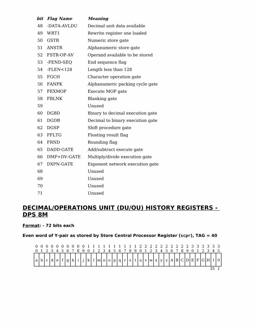
bit Flag Name Meaning
48 -DATA-AVLDU Decimal unit data available
49 WRT1 Rewrite register one loaded
50 GSTR Numeric store gate
51 ANSTR Alphanumeric store gate
52 FSTR-OP-AV Operand available to be stored
53 -FEND-SEQ End sequence flag
54 -FLEN<128 Length less than 128
55 FGCH Character operation gate
56 FANPK Alphanumeric packing cycle gate
57 FEXMOP Execute MOP gate
58 FBLNK Blanking gate
59 Unused
60 DGBD Binary to decimal execution gate
61 DGDB Decimal to binary execution gate
62 DGSP Shift procedure gate
63 FFLTG Floating result flag
64 FRND Rounding flag
65 DADD-GATE Add/subtract execute gate
66 DMP+DV-GATE Multiply/divide execution gate
67 DXPN-GATE Exponent network execution gate
68 Unused
69 Unused
70 Unused
71 Unused
DECIMAL/OPERATIONS UNIT (DU/OU) HISTORY REGISTERS - DPS 8M
Format: - 72 bits each
Even word of Y-pair as stored by Store Central Processor Register (scpr), TAG = 40
00
a
01
b
02
c
03
d
04
e
05
f
06
g
07
h
08
i
09
j
10
k
11
l
12
m
13
n
14
o
15
p
16
q
17
r
18
s
19
t
20
u
21
v
22
w
23
x
24
y
25
z
26
A
27
B
28
C
29
D
30
E
31
F
32
G
33
H
34
I
35
35
0
1
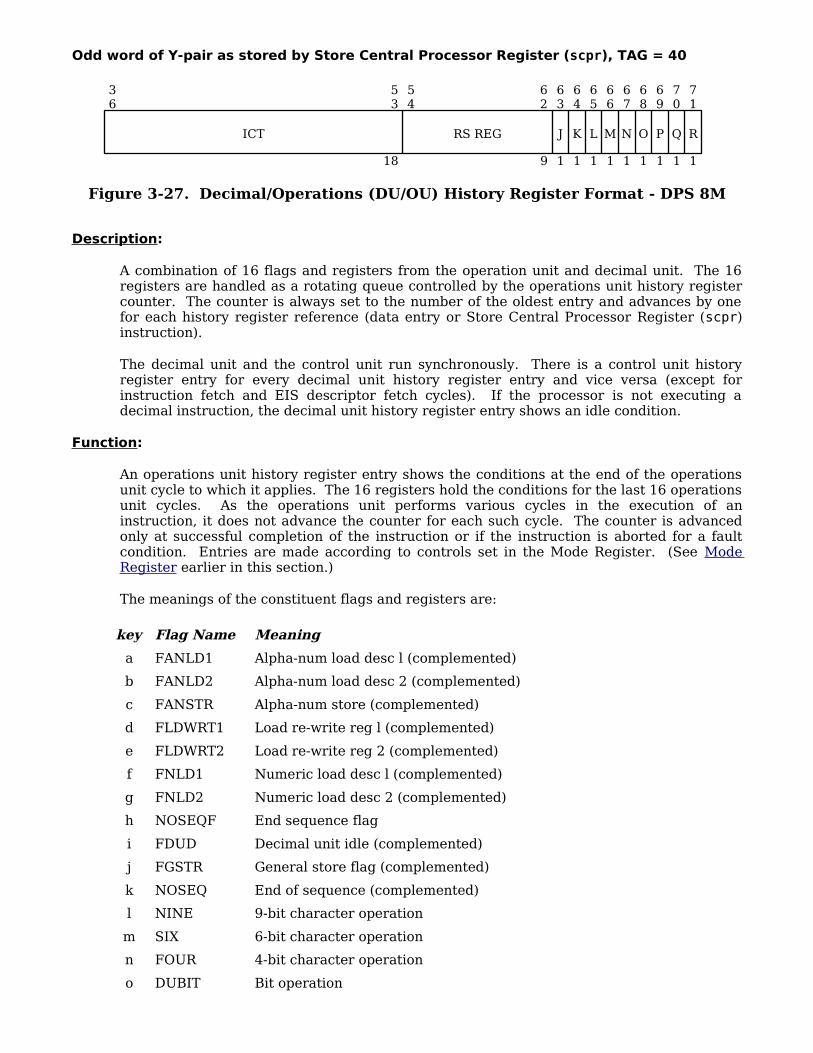
Odd word of Y-pair as stored by Store Central Processor Register (scpr), TAG = 40
Figure 3-27. Decimal/Operations (DU/OU) History Register Format - DPS 8M
Description:
A combination of 16 flags and registers from the operation unit and decimal unit. The 16 registers are handled as a rotating queue controlled by the operations unit history register counter. The counter is always set to the number of the oldest entry and advances by one for each history register reference (data entry or Store Central Processor Register (scpr) instruction).
The decimal unit and the control unit run synchronously. There is a control unit history register entry for every decimal unit history register entry and vice versa (except for instruction fetch and EIS descriptor fetch cycles). If the processor is not executing a decimal instruction, the decimal unit history register entry shows an idle condition.
Function:
An operations unit history register entry shows the conditions at the end of the operations unit cycle to which it applies. The 16 registers hold the conditions for the last 16 operations unit cycles. As the operations unit performs various cycles in the execution of an instruction, it does not advance the counter for each such cycle. The counter is advanced only at successful completion of the instruction or if the instruction is aborted for a fault condition. Entries are made according to controls set in the Mode Register. (See Mode Register earlier in this section.)
The meanings of the constituent flags and registers are:
key Flag Name Meaning
a FANLD1 Alpha-num load desc l (complemented)
b FANLD2 Alpha-num load desc 2 (complemented)
c FANSTR Alpha-num store (complemented)
d FLDWRT1 Load re-write reg l (complemented)
e FLDWRT2 Load re-write reg 2 (complemented)
f FNLD1 Numeric load desc l (complemented)
g FNLD2 Numeric load desc 2 (complemented)
h NOSEQF End sequence flag
i FDUD Decimal unit idle (complemented)
j FGSTR General store flag (complemented)
k NOSEQ End of sequence (complemented)
l NINE 9-bit character operation
m SIX 6-bit character operation
n FOUR 4-bit character operation
o DUBIT Bit operation
36
53
ICT
18
54
62
RS REG
9
63
J
1
64
K
1
65
L
1
66
M
1
67
N
1
68
O
1
69
P
1
70
Q
1
71
R
1
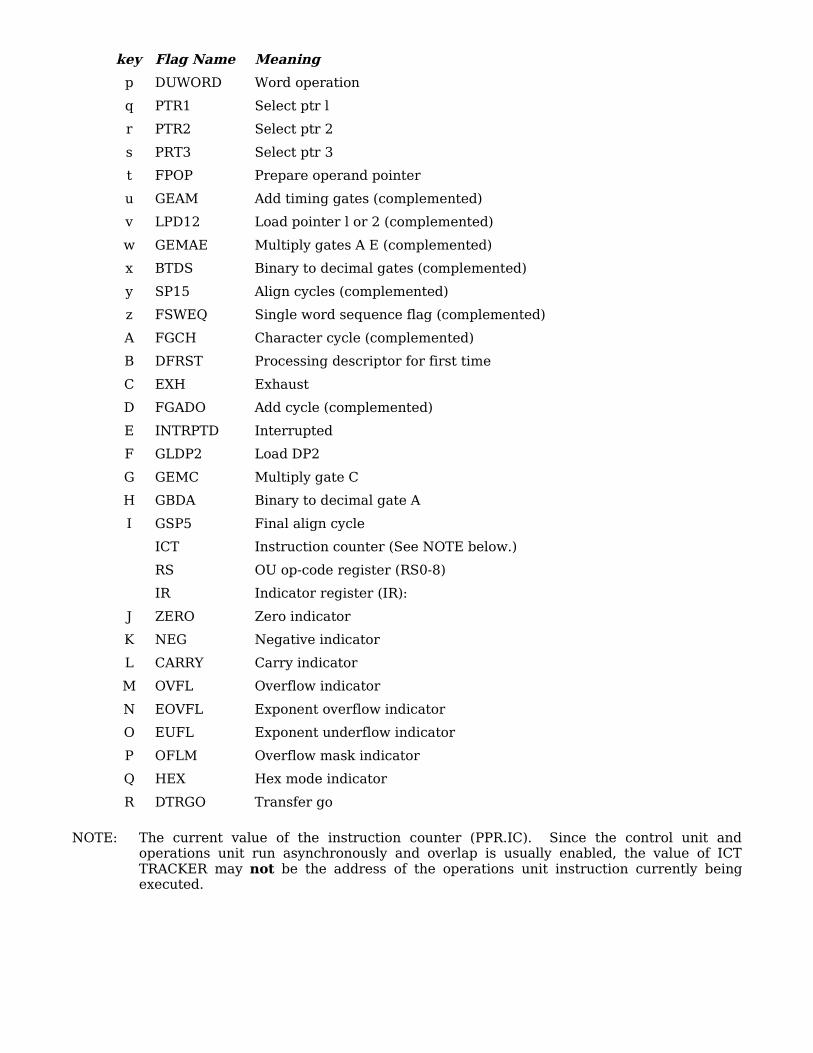
key Flag Name Meaning
p DUWORD Word operation
q PTR1 Select ptr l
r PTR2 Select ptr 2
s PRT3 Select ptr 3
t FPOP Prepare operand pointer
u GEAM Add timing gates (complemented)
v LPD12 Load pointer l or 2 (complemented)
w GEMAE Multiply gates A E (complemented)
x BTDS Binary to decimal gates (complemented)
y SP15 Align cycles (complemented)
z FSWEQ Single word sequence flag (complemented)
A FGCH Character cycle (complemented)
B DFRST Processing descriptor for first time
C EXH Exhaust
D FGADO Add cycle (complemented)
E INTRPTD Interrupted
F GLDP2 Load DP2
G GEMC Multiply gate C
H GBDA Binary to decimal gate A
I GSP5 Final align cycle
ICT Instruction counter (See NOTE below.)
RS OU op-code register (RS0-8)
IR Indicator register (IR):
J ZERO Zero indicator
K NEG Negative indicator
L CARRY Carry indicator
M OVFL Overflow indicator
N EOVFL Exponent overflow indicator
O EUFL Exponent underflow indicator
P OFLM Overflow mask indicator
Q HEX Hex mode indicator
R DTRGO Transfer go
NOTE: The current value of the instruction counter (PPR.IC). Since the control unit and operations unit run asynchronously and overlap is usually enabled, the value of ICT TRACKER may not be the address of the operations unit instruction currently being executed.

APPENDING UNIT (APU) HISTORY REGISTERS - DPS AND L68
Format: - 72 bits each
Even word of Y-pair as stored by Store Central Processor Register (scpr), TAG = 00
Odd word of Y-pair as stored by Store Central Processor Register (scpr), TAG = 00
Figure 3-28. Appending Unit (APU) History Register Format - DPS and L68
Description:
A combination of 16 flags and registers from the appending unit. The 16 registers are handled as a rotating queue controlled by the appending unit history register counter. The counter is always set to the number of the oldest entry and advances by one for each history register reference (data entry or Store Central Processor Register (scpr) instruction).
Function:
An appending unit history register entry shows the conditions in the appending unit at the end of an address preparation cycle in appending mode. The 16 registers hold the conditions for the last 16 such address preparation cycles. Entries are made according to controls set in the Mode Register. (See Mode Register earlier in this section.)
The meanings of the constituent flags and registers are:
key Flag Name Meaning
ESN Effective segment number (TPR.TSR)
a BSY Data source for ESN00 = from PPR.PSR01 = from PRn.SNR10 = from TPR.TSR11 = not used
b FDSPTW Descriptor segment PTW fetch
c MDSPTW Descriptor segment PTW modification
d FSDWP SDW fetch from paged descriptor segment
e FPTW PTW fetch
f FPTW2 PTW+1 fetch (prepaging for certain EIS instructions)
g MPTW PTW modification
00
14
ESN
15
15
16
a
2
17
b
1
18
c
1
19
d
1
20
e
1
21
f
1
22
g
1
23
h
1
24
i
1
25
j
1
26
29
SDWAMR
4
30
k
1
31
34
PTWAMR
4
35
l
1
36
59
ADD
24
60
TRR
62
3
63
0 0
65
0
3
66
m
1
67
0 0
69
0
3
70
n
1
71
0
1

key Flag Name Meaning
h FANP Final address fetch from nonpaged segment
i FAP Final address fetch from paged segment
j SDWAMM SDWAM match occurred
SDWAMR SDWAM register number if SDWAMM=1
k PTWAMM PTWAM match occurred
PTWAMR PTWAM register number if PTWAMM=1
l FLT Access violation or directed fault on this cycle
ADD 24-bit absolute main memory address from this cycle
TRR Ring number from this cycle (TPR.TRR)
m Multiple match error in SDWAM
n CA Segment is encacheable
p Multiple match error in PTWAM
r FHLD An access violation or directed fault is waiting
APPENDING UNIT (APU) HISTORY REGISTERS – DPS 8M
Format: - 72 bits each
Even word of Y-pair as stored by Store Central Processor Register (scpr), TAG = 00
Odd word of Y-pair as stored by Store Central Processor Register (scpr), TAG = 00
00
14
ESN
15
15
a
1
16
b
1
17
c
1
18
d
1
19
e
1
20
f
1
21
g
1
22
h
1
23
i
1
24
j
1
25
k
1
26
l
1
27
28
BSY
2
29
m
1
30
m1
31
2
32
n
34
3
35
o
1
36
59
RMA
24
60
p
62
3
63
q
1
64
r
65
2
66
s
1
67
t
1
68
69
u
2
70
v
1
71
w
1
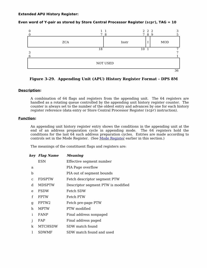
Extended APU History Register:
Even word of Y-pair as stored by Store Central Processor Register (scpr), TAG = 10
Figure 3-29. Appending Unit (APU) History Register Format - DPS 8M
Description:
A combination of 64 flags and registers from the appending unit. The 64 registers are handled as a rotating queue controlled by the appending unit history register counter. The counter is always set to the number of the oldest entry and advances by one for each history register reference (data entry or Store Central Processor Register (scpr) instruction).
Function:
An appending unit history register entry shows the conditions in the appending unit at the end of an address preparation cycle in appending mode. The 64 registers hold the conditions for the last 64 such address preparation cycles. Entries are made according to controls set in the Mode Register. (See Mode Register earlier in this section.)
The meanings of the constituent flags and registers are:
key Flag Name Meaning
ESN Effective segment number
a PIA Page overflow
b PIA out of segment bounds
c FDSPTW Fetch descriptor segment PTW
d MDSPTW Descriptor segment PTW is modified
e FSDW Fetch SDW
f FPTW Fetch PTW
g FPTW2 Fetch pre-page PTW
h MPTW PTW modified
i FANP Final address nonpaged
j FAP Final address paged
k MTCHSDW SDW match found
l SDWMF SDW match found and used
00
17
ZCA
18
18
27
Instr
10
28
I
1
29
35
MOD
736
36
71
NOT USED
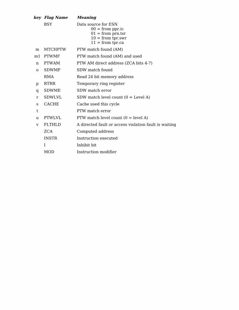
key Flag Name Meaning
BSY Data source for ESN00 = from ppr.ic01 = from prn.tsr10 = from tpr.swr11 = from tpr.ca
m MTCHPTW PTW match found (AM)
m1 PTWMF PTW match found (AM) and used
n PTWAM PTW AM direct address (ZCA bits 4-7)
o SDWMF SDW match found
RMA Read 24 bit memory address
p RTRR Temporary ring register
q SDWME SDW match error
r SDWLVL SDW match level count (0 = Level A)
s CACHE Cache used this cycle
t PTW match error
u PTWLVL PTW match level count (0 = level A)
v FLTHLD A directed fault or access violation fault is waiting
ZCA Computed address
INSTR Instruction executed
I Inhibit bit
MOD Instruction modifier
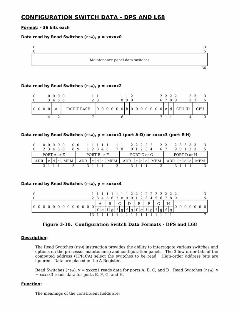
CONFIGURATION SWITCH DATA - DPS AND L68
Format: - 36 bits each
Data read by Read Switches (rsw), y = xxxxx0
Data read by Read Switches (rsw), y = xxxxx2
Data read by Read Switches (rsw), y = xxxxx1 (port A-D) or xxxxx3 (port E-H)
Data read by Read Switches (rsw), y = xxxxx4
Figure 3-30. Configuration Switch Data Formats - DPS and L68
Description:
The Read Switches (rsw) instruction provides the ability to interrogate various switches and options on the processor maintenance and configuration panels. The 3 low-order bits of the computed address (TPR.CA) select the switches to be read. High-order address bits are ignored. Data are placed in the A Register.
Read Switches (rsw), y = xxxxx1 reads data for ports A, B, C, and D. Read Switches (rsw), y = xxxxx3 reads data for ports E, F, G, and H.
Function:
The meanings of the constituent fields are:
00
36
35
Maintenance panel data switches
00
0 0 0
03
0
4
04
05
a
2
06
FAULT BASE
12
7
13
0 0 0 0 0
18
0
6
19
b
1
20
0 0 0 0 0 0
26
0
7
27
c
1
28
d
1
29
CPU ID
32
4
33
CPU
35
3
00
ADR
02
3
03
c1
04
d1
05
e1
06
MEM
08
3
09
ADR
11
3
12
c1
13
d1
14
e1
15
MEM
17
3
18
ADR
20
3
21
c1
22
d1
23
e1
24
MEM
26
3
27
ADR
29
3
30
c1
31
d1
32
e1
33
MEM
35
3
PORT A or E PORT B or F PORT C or G PORT D or H
00
0 0 0 0 0 0 0 0 0 0 0 0
12
0
13
13
f1
14
g1
15
f1
16
g1
17
f1
18
g1
19
f1
20
g1
21
f1
22
g1
23
f1
24
g1
25
f1
26
g1
27
f1
28
g1
29
0 0 0 0 0 0
35
0
7
A B C D E F G H

key Field Name Meaning
a CPU-Type Equals "00" for a L68 or a DPS processor.
FLT BASE The seven MSB of the 12-bit fault base address
b dps_option Processor option0 = L68 processor1 = DPS processor
c cache 2K cache option0 = disabled1 = enabled
d ext_gcos GCOS mode extended memory option0 = disabled1 = enabled
CPU_ID These bit positions have a configuration of "1110" for a L68 or a DPS CPU.
CPU Processor number from processor configuration panel number switches.
PORT A or E, etc. Port data fields further substructured as:
ADR Address assignment switch setting for port
c Port enabled flag
d System initialize enabled flag
e Interlace enabled flag
MEM Coded memory size . . .
000001010011100101110111
32K64K128K256K512K1024K2048K4096K
A, B, etc. Port data fields further substructured as:
f Interlace mode0 = 4 word if interlace enabled for port1 = 2 word if interlace enabled for port
g Main memory size0 = full, all of MEM is configured1 = half, half of MEM is configured
CONFIGURATION SWITCH DATA - DPS 8M
The following changes apply to the DPS 8M processor.
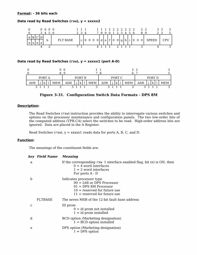
Format: - 36 bits each
Data read by Read Switches (rsw), y = xxxxx2
Data read by Read Switches (rsw), y = xxxxx1 (port A-D)
Figure 3-31. Configuration Switch Data Formats - DPS 8M
Description:
The Read Switches (rsw) instruction provides the ability to interrogate various switches and options on the processor maintenance and configuration panels. The two low-order bits of the computed address (TPR.CA) select the switches to be read. High-order address bits are ignored. Data are placed in the A Register.
Read Switches (rsw), y = xxxxx1 reads data for ports A, B, C, and D.
Function:
The meanings of the constituent fields are:
key Field Name Meaning
a If the corresponding rsw 1 interface enabled flag, bit (e) is ON, then0 = 4 word interfaces1 = 2 word interfacesFor ports A - D
b Indicates processor type00 = L68 or DPS Processor01 = DPS 8M Processor10 = reserved for future use11 = reserved for future use
FLTBASE The seven MSB of the 12-bit fault base address
c ID prom0 = id prom not installed1 = id prom installed
d BCD option (Marketing designation)1 = BCD option installed
e DPS option (Marketing designation)1 = DPS option
00
a a a
03
a4
04
05
b
2
06
FLT BASE
12
7
13
c
1
14
0 0 0
17
0
4
18
d
1
19
e
1
20
f
1
21
0
22
0
2
23
g
1
24
h
1
25
i
1
26
0 0
28
0
3
29
SPEED
32
4
33
CPU
35
3
A B C D
00
ADR3
j1
k1
l1
MEM
08
3
09
ADR3
j1
k1
l1
MEM
17
3
18
ADR3
j1
k1
l1
MEM
26
3
27
ADR3
j1
k1
l1
MEM
35
3
PORT A PORT B PORT C PORT D
key Field Name Meaning
f 8K cache1 = 8K cache installed
g DPS 8M Processor type designation1 = DPS 8/xxM0 = DPS 8/xx
h GCOS/VMS switch position1 = Virtual Mode0 = GCOS Mode
i Current or new product line peripheral type1 = NPL0 = CPL
SPEED Processor speed options0000 = 8/700100 = 8/52
CPU Processor number
ADR Address assignment switch setting for port
j Port enabled flag
k System initialize enabled flag
l Interface enabled flag
MEM Coded memory size:
000001010011100101110111
32K64K128K256K512K1024K2048K4096K
CONTROL UNIT DATA
Format: - 288 bits, 8 machine words
Data as stored by Store Control Unit (scu) instruction
Word
00
PRR
02
3
03
17
PSR
15
18
a
1
19
b
1
20
c
1
21
d
1
22
e
1
23
f
1
24
g
1
25
h
1
26
i
1
27
j
1
28
k
1
29
l
1
30
m
1
31
n
1
32
o
1
33
FCT
35
3
0
00
a
1
01
b
1
02
c
1
03
d
1
04
e
1
05
f
1
06
g
1
07
h
1
08
i
1
09
j
1
10
k
1
11
l
1
12
m
1
13
n
1
14
o
1
15
p
1
16
q
1
17
r
1
18
s
1
19
t
1
20
IA
23
4
24
IACHN
26
3
27
CNCHN
29
3
30
F/I ADDR
34
5
35
u
1
1
Figure 3-32. Control Unit Data Format
Description:
A collection of flags and registers from the appending unit and the control unit. In general, the data has valid meaning only when stored with the Store Control Unit (scu) instruction as the first instruction of a fault or interrupt trap pair.
Function:
The control unit data allows the processor to restart an instruction at the point of interruption when it is interrupted by an access violation fault, a directed fault, or (for certain EIS instructions) an interrupt. Directed faults are intentional, and most access violation faults and interrupts are recoverable. If the interruption is not recoverable, the control unit data provides enough information to determine the exact nature of the error.
Instruction execution restarts immediately upon execution of a Restore Control Unit (rcu) instruction referencing the Y-block8 area into which the control unit data was stored.
00
TRR
02
3
03
17
TSR
15
18
a
19
b
20
c
21
d4
22
e
23
f
24
25
4
26
0
1
27
CPU
29
3
30
35
DELTA
6
2PTW SDW
g h
00
0 0 0 0 0 0 0 0 0 0 0 0 0 0 0 0 0
17
0
18
18
a
20
3
21
b1
22
a
24
3
25
b1
26
a
28
3
29
b1
30
TEMP BIT
35
6
3TSNA TSNB TSNC
00
17
IC
18
18
a
1
19
b
1
20
c
1
21
d
1
22
e
1
23
f
1
24
g
1
25
h
1
26
i
1
27
j
1
28
k
1
29
l
1
30
m
1
31
n
1
32
0 0 0
35
0
4
4
00
17
COMPUTED ADDRESS
18
18
a
1
19
b
1
20
c
1
21
d
1
22
e
1
23
f
1
24
g
1
25
h
1
26
i
1
27
j
1
28
k
1
29
l
1
30
35
CT HOLD
6
5
00
17
ADDRESS
18
18
27
OPCODE
10
28
I
1
29
P
1
30
35
TAG
6
6
00
17
ADDRESS
18
18
27
OPCODE
10
28
I
1
29
P
1
30
35
TAG
6
7
Fields having an "x" in the column headed L are not restored by the Restore Control Unit (rcu) instruction.
The meanings of the constituent fields are:
Word key L Field Name Meaning
0 PRR Procedure ring register (PPR.PRR)
0 PSR Procedure segment register (PPR.PSR)
0 a P Privileged bit (PPR.P)
0 b XSF External segment flag
0 c x SDWAMM Match on SDWAM
0 d x SD-ON SDWAM enabled
0 e x PTWAMM Match on PTWAM
0 f x PT-ON PTWAM enabled
0 g x PI-AP Instruction fetch append cycle
0 h x DSPTW Fetch descriptor segment PTW
0 i x SDWNP Fetch SDW - nonpaged
0 j x SDWP Fetch SDW - paged
0 k x PTW Fetch PTW
0 l x PTW2 Fetch prepage PTW
0 m x FAP Fetch final address - paged
0 n x FANP Fetch final address - nonpaged
0 o x FABS Fetch final address - absolute
0 FCT Fault counter - counts retries
1 a xx
IROISN
For access violation fault - illegal ring orderFor store fault - illegal segment number
1 b xx
ORBIOC
For access violation fault - out of execute bracketFor illegal procedure fault - illegal op code
1 c xx
E-OFFIA+IM
For access violation fault - execute bit is OFFFor illegal procedure fault - illegal address or modifier
1 d xx
ORBISP
For access violation fault - out of read bracketFor illegal procedure fault - illegal slave procedure
1 e xx
R-OFFIPR
For access violation fault - read bit is OFFFor illegal procedure fault - illegal EIS digit
1 f xx
OWBNEA
For access violation fault - out of write bracketFor store fault - nonexistent address
1 g xx
W-OFFOOB
For access violation fault - write bit is OFFFor store fault - out of bounds (BAR mode)
1 h x NO GA For access violation fault - not a gate
1 i x OCB For access violation fault - out of call bracket
1 j x OCALL For access violation fault - outward call
1 k x BOC For access violation fault - bad outward call
1 l x PTWAM_ER For access violation fault - on DPS 8M processors, a PTW associative memory error. Not used on DPS/L68 processors.

Word key L Field Name Meaning
1 m x CRT For access violation fault - cross ring transfer
1 n x RALR For access violation fault - ring alarm
1 o x SDWAM_ER For access violation fault - on DPS 8M an SDW associative memory error. An associative memory error on DPS/L68.
1 p x OOSB For access violation fault - out of segment bounds
1 q x PARU For parity fault - processor parity upper
1 r x PARL For parity fault - processor parity lower
1 s x ONC1 For operation not complete fault – processor/system controller sequence error #1
1 t x ONC2 For operation not complete fault – processor/system controller sequence error #2
1 x IA System controller illegal action lines (see Table 3-2)
1 x IACHN Illegal action processor port
1 x CNCHN For connect fault - connect processor port
1 x F/I ADDR Modulo 2 fault/interrupt vector address
1 u x F/I Fault/interrupt flag0 = interrupt1 = fault
2 TRR Temporary ring register (TPR.TRR)
2 TSR Temporary segment register (TPR.TSR)
PTW DPS 8M processors only; this field mbz on DPS/L68 processors:
2222
abcd
x x x x
PTWAM levels A, B enabled (enabled = 1)PTWAM levels C, D enabledPTWAM levels A, B match (match = 1)PTWAM levels C, D match
SDW DPS 8M processors only; this field mbz on DPS/L68 processors:
2222
efgh
xxxx
SDWAM levels A, B enabledSDWAM levels C, D enabledSDWAM levels A, B matchSDWAM levels C, D match
2 CPU CPU number
2 DELTA Address increment for repeats
3 TSNA Pointer register number for non-EIS operands or for EIS operand #1 further substructured as:
3 a PRNO Pointer register number
3 b ---- 1 = PRNO is valid
3 TSNB Pointer register number for EIS operand #2 further substructured as for TSNA above
3 TSNC Pointer register number for EIS operand #3 further substructured as for TSNA above
3 TEMP BIT Current bit offset (TPR.TBR)
4 IC Instruction counter (PPR.IC)
4 a ZERO Zero indicator

Word key L Field Name Meaning
4 b NEG Negative indicator
4 c CARY Carry indicator
4 d OVFL Overflow indicator
4 e EOVF Exponent overflow indicator
4 f EUFL Exponent underflow indicator
4 g OFLM Overflow mask indicator
4 h TRO Tally runout indicator
4 i PAR Parity error indicator
4 j PARM Parity mask indicator
4 k -BM Not BAR mode indicator
4 l TRU EIS truncation indicator
4 m MIF Mid-instruction interrupt indicator
4 n ABS Absolute mode indicator
4 o HEX Hex mode indicator (DPS 8M processors only)
5 x CA Current computed address (TPR.CA)
5 a RF First cycle of all repeat instructions
5 b RPT Execute a Repeat (rpt) instruction
5 c RD Execute a Repeat Double (rpd) instruction
5 d RL Execute a Repeat Link (rpl) instruction
5 e POT Prepare operand tally. This flag is up until the indirect word of an indirect then tally address modifier is successfully fetched.
5 f PON Prepare operand no tally. This flag is up until the indirect word of a return type transfer instruction is successfully fetched. It indicates that there is no indirect chain even though an indirect fetch is being performed.
5 g XDE Execute instruction from Execute Double even pair
5 h XDO Execute instruction from Execute Double odd pair
5 i ITP Execute ITP indirect cycle
5 j RFI Restart this instruction
5 k ITS Execute ITS indirect cycle
5 l FIF Fault occurred during instruction fetch
5 CT HOLD Contents of the modifier holding register
6 Word 6 is the contents of the working instruction register and reflects conditions at the exact point of address preparation when the fault or interrupt occurred. The ADDRESS and TAG fields are replaced with data from pointer registers, indirect pointers, and/or indirect words during each indirect cycle. Each instruction of the current pair is moved to this register before actual address preparation begins.
Word key L Field Name Meaning
7 Word 7 is the contents of the instruction holding register. It contains the odd word of the last instruction pair fetched from main memory. Note that, primarily because of overlap, this instruction is not necessarily paired with the instruction in word 6.
DECIMAL UNIT DATA
Format: - 288 bits, 8 machine words
Data as stored by Store Pointers and Lengths (spl) instruction
Word
00
0 0 0 0 0 0 0 0
08
0
9
09
Z
1
10
Ø
1
11
0
1
35
CH TALLY
24
0
12
00
0 0 0 0 0 0 0 0 0 0 0 0 0 0 0 0 0 0 0 0 0 0 0 0 0 0 0 0 0 0 0 0 0 0 0
35
0
36
1
00
23
D1 PTR
24
24
0
1
25
26
TA
2
27
0 0
29
0
3
30
I
1
31
F
1
32
A
1
33
0 0
35
0
3
2
00
09
LEVEL 1
10
10
0
11
0
2
12
35
D1 RES
24
3
00
23
D2 PTR
24
24
0
1
25
26
TA
2
27
0 0
29
0
3
30
R
1
31
F
1
32
A
1
33
0 0
35
0
3
4
00
09
LEVEL 2
10
10
0
11
0
2
12
35
D2 RES
24
5
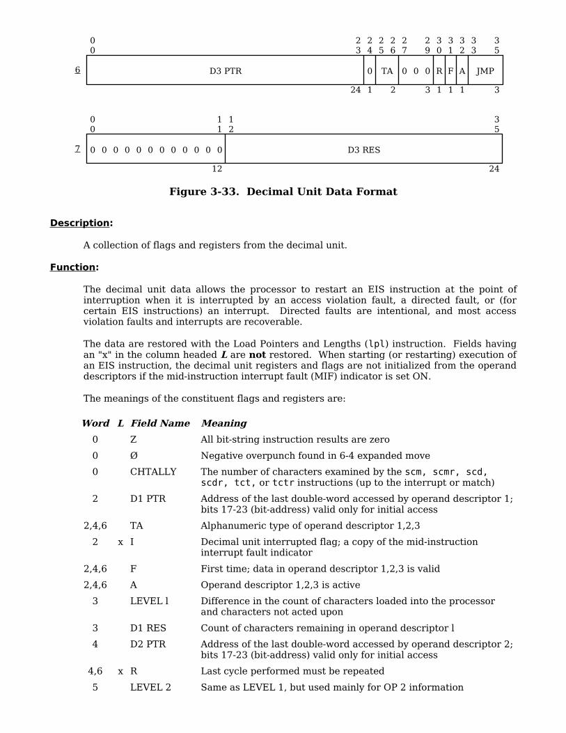
Figure 3-33. Decimal Unit Data Format
Description:
A collection of flags and registers from the decimal unit.
Function:
The decimal unit data allows the processor to restart an EIS instruction at the point of interruption when it is interrupted by an access violation fault, a directed fault, or (for certain EIS instructions) an interrupt. Directed faults are intentional, and most access violation faults and interrupts are recoverable.
The data are restored with the Load Pointers and Lengths (lpl) instruction. Fields having an "x" in the column headed L are not restored. When starting (or restarting) execution of an EIS instruction, the decimal unit registers and flags are not initialized from the operand descriptors if the mid-instruction interrupt fault (MIF) indicator is set ON.
The meanings of the constituent flags and registers are:
Word L Field Name Meaning
0 Z All bit-string instruction results are zero
0 Ø Negative overpunch found in 6-4 expanded move
0 CHTALLY The number of characters examined by the scm, scmr, scd, scdr, tct, or tctr instructions (up to the interrupt or match)
2 D1 PTR Address of the last double-word accessed by operand descriptor 1; bits 17-23 (bit-address) valid only for initial access
2,4,6 TA Alphanumeric type of operand descriptor 1,2,3
2 x I Decimal unit interrupted flag; a copy of the mid-instruction interrupt fault indicator
2,4,6 F First time; data in operand descriptor 1,2,3 is valid
2,4,6 A Operand descriptor 1,2,3 is active
3 LEVEL l Difference in the count of characters loaded into the processor and characters not acted upon
3 D1 RES Count of characters remaining in operand descriptor l
4 D2 PTR Address of the last double-word accessed by operand descriptor 2; bits 17-23 (bit-address) valid only for initial access
4,6 x R Last cycle performed must be repeated
5 LEVEL 2 Same as LEVEL 1, but used mainly for OP 2 information
00
23
D3 PTR
24
24
0
1
25
26
TA
2
27
0 0
29
0
3
30
R
1
31
F
1
32
A
1
33
JMP
35
3
6
00
0 0 0 0 0 0 0 0 0 0 0
11
0
12
12
35
D3 RES
24
7

Word L Field Name Meaning
5 D2 RES Count of characters remaining in operand descriptor 2
6 D3 PTR Address of the last double-word accessed by operand descriptor 3; bits 17-23 (bit-address) valid only for initial access
6 JMP Descriptor count; number of words to skip to find the next instruction following this multiword instruction
7 D3 RES Count of characters remaining in operand descriptor 3

SECTION 4: MACHINE INSTRUCTIONS
This section describes the complete set of machine instructions for the Multics processor. The presentation assumes that the reader is familiar with the general structure of the processor, the representation of information, the data formats, and the method of address preparation. Additional information on these subjects appears near the beginning of this section and in Sections 2, 3, 5, and 6.
INSTRUCTION REPERTOIRE
The processor interprets a 10-bit field of the instruction word as the operation code. This field size yields 1024 possible instructions of which 547 are implemented. There are 456 basic operations and 91 extended instruction set (EIS) operations.
Arrangement of Instructions
Instructions are presented alphabetically by their mnemonic codes within functional categories. An overall alphabetic listing of instruction codes and their names appears in Appendix B.
Basic Operations
The 456 basic operations in the processor all require exactly one 36-bit machine word. They are categorized as follows:
181 Fixed-point binary arithmetic
85 Boolean operations
34 Floating-point binary arithmetic
36 Transfer of control
75 Pointer register
17 Miscellaneous
28 Privileged
Extended Instruction Set (EIS) Operations
The 91 extended instruction set (EIS) operations are divided into 62 EIS single-word instructions and 29 EIS multiword instructions.
EIS Single-Word Operations
The 62 EIS single-word instructions load, store, and perform special arithmetic on the address registers (ARn) used to access bit- and character-string operands, and safe-store decimal unit (DU) control information required to service a processor fault or interrupt. Like the basic operations, EIS single-word instructions require exactly one 36-bit machine word.

EIS Multiword Operations
The 29 EIS multiword instructions perform decimal arithmetic and bit- and character-string operations. They require three or four 36-bit machine words depending on individual operand descriptor requirements.
FORMAT OF INSTRUCTION DESCRIPTION
Each instruction in the repertoire is described in the following pages of this section. The descriptions are presented in the format shown below.
MNEMONIC INSTRUCTION NAME OPCODE
FORMAT: Figure or figure reference
SUMMARY: Text and/or bit transfer equations
MODIFICATIONS: Text
INDICATORS: Text and/or logic statements
NOTES: Text
Line 1: MNEMONIC, INSTRUCTION NAME, OPCODE
This line has three parts that contain the following:
1. MNEMONIC -- The mnemonic code for the operation field of the assembler statement. The Multics assembler, ALM, recognizes this character string value and maps it into the appropriate binary pattern when generating the actual object code.
2. INSTRUCTION NAME -- The name of the machine instruction from which the mnemonic was derived.
3. OPCODE -- The octal value of the operation code for the instruction. A 0 or a 1 in parentheses following an octal code indicates whether bit 27 (opcode extension bit) of the instruction word is OFF or ON.
Line 2: FORMAT
The layout and definition of the subfields of the instruction word or words are given here either as a figure or as a reference to a figure.
Line 3: SUMMARY
The change in the state of the processor effected by the execution of the instruction is described in a short, symbolic form. If reference is made to the state of an indicator in the summary, it is the state of the indicator before the instruction is executed.
Line 4: MODIFICATIONS
Those modifiers that cannot be used with the instruction are listed explicitly as exceptions. See Section 6 for a discussion of address modification.

Line 5: INDICATORS
Only those indicators are listed whose state can be changed by the execution of the instruction. In most cases, a condition for setting ON as well as one for setting OFF is stated. If only one of the two is stated, then the indicator remains unchanged if the condition is not met. Unless stated otherwise, the conditions refer to the contents of registers existing after instruction execution. Refer also to "Common Attributes of Instructions," later in this section.
Line 6: NOTES
This part of the description exists only in those cases where the summary is not sufficient for in-depth understanding of the instruction.

DEFINITIONS OF NOTATION AND SYMBOLS
Main Memory Addresses
y an 18-bit computed address as generated during address preparation.
Y a 24-bit main memory address of the instruction operand after all address preparation (including appending) is complete.
Y-pair a pair of main memory locations with successive addresses, the smaller address being even. When Y is even, it designates the pair Y(even), Y+1; and when it is odd, the pair Y-1, Y(odd). The main memory location with the smaller (even) address contains the most significant part of a double-word operand or the first of a pair of instructions.
Y-blockn a block of main memory locations of 4-, 8-, 16-, or 32-word extent. For a block of n-word extent, the processor forces Y-blockn to a 0 modulo n address and performs address incrementing through the block accordingly, stopping when the address next reaches a value 0 modulo n.
Y-charnk a character or string of characters in main memory of character size n bits as described by the kth operand descriptor. n is specified by the data type field of operand descriptor k and may have values 4, 6, or 9. See Section 6 for details of operand descriptors.
Y-bitk a bit or string of bits in main memory as described by the kth operand descriptor. See Section 6 for details of operand descriptors.
Index Values
When reference is made to the elements of a string of characters or bits in main memory, the notation shown in "Register Position and Contents" below is used. The index used to show traversing a string of extent n may take any of the values in the interval (1,n) unless noted otherwise. The elements of a main memory block are traversed explicitly by using the index as an addend to the given block address, (e.g., Y-block8+m and Y-block4+2m+1).
Abbreviations and Symbols
A Accumulator register
ARn Address register n (n = 0, 1, 2, ..., 7)
AQ Combined accumulator-quotient register
BAR Base address register
C( ) "Contents of"
CA Computed address
DSBR Descriptor segment base register
DSBR.ADDR Address field of DSBR
DSBR.BND Bound field of DSBR
DSBR.STACK Stack base field of DSBR
DSBR.U Unpaged flag of DSBR

E Exponent register
EA Combined exponent-accumulator register
EAQ Combined exponent-accumulator-quotient register
ERN Effective ring number
ESN Effective segment number
IC Instruction counter
IR Indicator register
PPR Procedure pointer register
PPR.PRR Procedure ring register of PPR
PPR.PSR Procedure segment register of PPR
PPR.IC Instruction counter register of PPR (same as IC above)
PPR.P Privileged flag of PPR
PRn Pointer register n (n = 0, 1, 2, ..., 7)
PRn.RNR Ring number register of PRn
PRn.SNR Segment number register of PRn
PRn.WORDNO Word address register of PRn
PRn.CHAR Character address register of PRn
PRn.BITNO Bit offset register of PRn
Q Quotient register
PTWAM Page table word associative memory
SDWAM Segment descriptor word associative memory
RALR Ring alarm register
TPR Temporary pointer register
TPR.CA Computed address register of TPR (same as CA above)
TPR.TRR Temporary ring register of TPR
TPR.TSR Temporary segment register of TPR
TPR.TBR Temporary bit register of TPR
TR Timer register
Xn Index register n (n = 0, 1, 2, ..., 7)
Z Temporary pseudo-result of a nonstore comparative operation
Register Positions and Contents
In the definitions that follow, "R" stands for any of the registers listed above, as well as for main memory words, word-pairs, word-blocks, and bit- or character-strings.
Ri The ith bit, character, or byte position of R
R(i) The ith register of a set of n registers named R
Ri,j The bit, character, or byte positions i through j of R
C(R) The contents of the full register R
C(R)i The contents of the ith bit, character, or byte of R
C(R)i,j The contents of the bits, characters, or bytes i through j of R
xx...x A string of binary bits (0's or l's) of any necessary length
When the description of an instruction specifies a change for a part of a register or main memory location, it is understood that the part of the register or main memory location not mentioned remains unchanged.
Other Symbols
→ replaces
:: compare with
& the Boolean connective AND
| the Boolean connective OR
⊕ the Boolean connective NON-EQUIVALENCE (or EXCLUSIVE OR)
~XXX the logical inverse (ones complement) of the quantity XXX
≠ not equal
n**m indicates exponentiation (n and m are integers); for example, the fifth power of 2 is represented as 2**5.
× multiplication; for example, C(Y) times C(Q) is represented as C(Y) × C(Q)
/ division; for example, C(Y) divided by C(A) is represented as C(Y) / C(A).
|| concatenation; for example, string1 || string2.
| ... | the absolute value of the value between vertical bars (no algebraic sign). For example the absolute value of C(A) plus C(Y) is represented as: | C(A) + C(Y) | .
C(R)modn A coined notation for remaindering or modulo arithmetic; for example C(REG) modulo 9 is represented as C(REG)mod9
COMMON ATTRIBUTES OF INSTRUCTIONS
Illegal Modification
If an illegal modifier is used with any instruction, an illegal procedure fault with a subcode class of illegal modifier occurs.
Parity Indicator
The parity indicator is turned ON at the end of a main memory access that has incorrect parity.
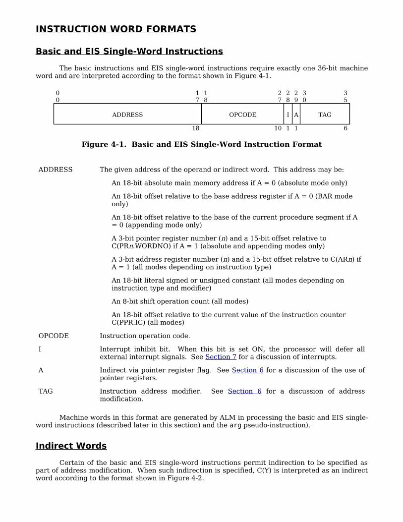
INSTRUCTION WORD FORMATS
Basic and EIS Single-Word Instructions
The basic instructions and EIS single-word instructions require exactly one 36-bit machine word and are interpreted according to the format shown in Figure 4-1.
Figure 4-1. Basic and EIS Single-Word Instruction Format
ADDRESS The given address of the operand or indirect word. This address may be:
An 18-bit absolute main memory address if A = 0 (absolute mode only)
An 18-bit offset relative to the base address register if A = 0 (BAR mode only)
An 18-bit offset relative to the base of the current procedure segment if A = 0 (appending mode only)
A 3-bit pointer register number (n) and a 15-bit offset relative to C(PRn.WORDNO) if A = 1 (absolute and appending modes only)
A 3-bit address register number (n) and a 15-bit offset relative to C(ARn) if A = 1 (all modes depending on instruction type)
An 18-bit literal signed or unsigned constant (all modes depending on instruction type and modifier)
An 8-bit shift operation count (all modes)
An 18-bit offset relative to the current value of the instruction counter C(PPR.IC) (all modes)
OPCODE Instruction operation code.
I Interrupt inhibit bit. When this bit is set ON, the processor will defer all external interrupt signals. See Section 7 for a discussion of interrupts.
A Indirect via pointer register flag. See Section 6 for a discussion of the use of pointer registers.
TAG Instruction address modifier. See Section 6 for a discussion of address modification.
Machine words in this format are generated by ALM in processing the basic and EIS single-word instructions (described later in this section) and the arg pseudo-instruction).
Indirect Words
Certain of the basic and EIS single-word instructions permit indirection to be specified as part of address modification. When such indirection is specified, C(Y) is interpreted as an indirect word according to the format shown in Figure 4-2.
00
17
ADDRESS
18
18
OPCODE
27
10
28
I
1
29
A
1
30
35
TAG
6

Figure 4-2. Indirect Word Format
ADDRESS The given address of the operand or next indirect word. This address may be:
An 18-bit absolute main memory address if A = 0 in the instruction word (absolute mode only)
An 18-bit offset relative to the base address register (BAR) if A = 0 in the instruction word (BAR mode only)
An 18-bit offset relative to the base of the segment in which the word resides if A = 0 (appending mode only)
Three zero bits and a 15-bit segment number if TAG = (43)8 (ITS modification) (absolute and appending modes only)
A 3-bit pointer register number and 15 zero bits if TAG = (41)8 (ITP modification) (absolute and appending modes only)
TALLY A count field for use by those address modifiers that involve tallying
TAG This field may be (depending on the TAG value causing the indirection):
A 6-bit address modifier
A 6-bit increment to be added to or subtracted from ADDRESS on each reference
A 1-bit character mode (6- or 9-bit) flag, two 0 bits, and a 3-bit character position number
Machine words in this format may be generated by use of the ALM vfd pseudo-instruction.
EIS Multiword Instructions
The EIS multiword instructions require three or four machine words depending on the operand descriptor requirements of the individual instructions. The words are interpreted according to the format shown in Figure 4-3. The instruction descriptions (later in this section) contain ALM coding examples. Refer to the Multics Commands and Active Functions, Order No. AG92, "alm" command for additional information.
00
17
18
18
29
12
30
35
6
ADDRESS TALLY TAG
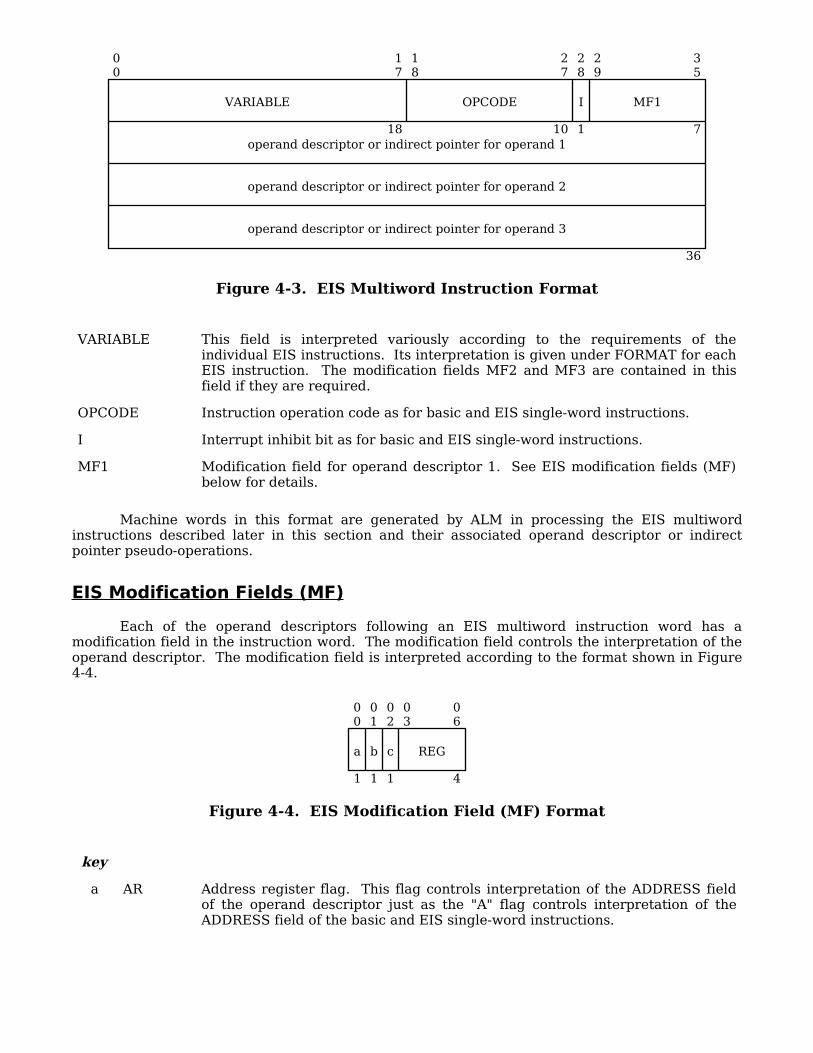
Figure 4-3. EIS Multiword Instruction Format
VARIABLE This field is interpreted variously according to the requirements of the individual EIS instructions. Its interpretation is given under FORMAT for each EIS instruction. The modification fields MF2 and MF3 are contained in this field if they are required.
OPCODE Instruction operation code as for basic and EIS single-word instructions.
I Interrupt inhibit bit as for basic and EIS single-word instructions.
MF1 Modification field for operand descriptor 1. See EIS modification fields (MF) below for details.
Machine words in this format are generated by ALM in processing the EIS multiword instructions described later in this section and their associated operand descriptor or indirect pointer pseudo-operations.
EIS Modification Fields (MF)
Each of the operand descriptors following an EIS multiword instruction word has a modification field in the instruction word. The modification field controls the interpretation of the operand descriptor. The modification field is interpreted according to the format shown in Figure 4-4.
Figure 4-4. EIS Modification Field (MF) Format
key
a AR Address register flag. This flag controls interpretation of the ADDRESS field of the operand descriptor just as the "A" flag controls interpretation of the ADDRESS field of the basic and EIS single-word instructions.
00
17
18
27
28
29
35
VARIABLE
18
OPCODE I MF1
7operand descriptor or indirect pointer for operand 1
operand descriptor or indirect pointer for operand 2
operand descriptor or indirect pointer for operand 3
36
10 1
00
a
1
01
b
1
02
c
1
03
06
REG
4
b RL Register length control. If RL = 0, then the length (N) field of the operand descriptor contains the length of the operand. If RL = 1, then the length (N) field of the operand descriptor contains a selector value specifying a register holding the operand length. Operand length is interpreted as units of the data size (1-, 4-, 6-, or 9-bit) given in the associated operand descriptor.
c ID Indirect descriptor control. If ID = 1 for Mfk, then the kth word following the instruction word is an indirect pointer to the operand descriptor for the kth operand; otherwise, that word is the operand descriptor.
REG The register number for R-type modification (if any) of ADDRESS of the operand descriptor. These modifications are similar to R-type modifications for basic instructions and are summarized in Table 4-1. Illegal modifiers have the entry "IPR" and cause an illegal procedure fault.
Table 4-1. R-type Modifiers for REG Fields
Octal Code R-type MF.REG
Meaning as used in:
Indirect operand descriptor-pointer C(operand descriptor)32,35
00 n n n IPR
01 au au au au
02 qu qu qu qu
03 du IPR IPR du (a)
04 ic ic ic ic (b)
05 al a (c) al a (c)
06 ql q (c) ql q (c)
07 dl IPR IPR IPR
10 x0 x0 x0 x0
11 x1 x1 x1 x1
12 x2 x2 x2 x2
13 x3 x3 x3 x3
14 x4 x4 x4 x4
15 x5 x5 x5 x5
16 x6 x6 x6 x6
17 x7 x7 x7 x7
a) The du modifier is permitted only in the second operand descriptor of the scd, scdr, scm, and scmr instructions to specify that the test character(s) reside(s) in bits 0-18 of the operand descriptor.
b) The ic modifier is permitted in MFk.REG and C (od)32,35 only if MFk.RL = 0, that is, if the contents of the register is an address offset, not the designation of a register containing the operand length.
c) The limit of addressing extent of the processor is 2**18 words; that is, given an address, y, a modifier may be employed to access a main memory word anywhere in the range (y-2**17, y+2**17-1), provided other address range constraints are not violated. Since it is desirable to address this same extent as words, characters, and bits it is necessary to provide a register

with range greater than the 12 bits of N or the 18 bits of normal R-type modifiers. This is done by extending the range of the A and Q modifiers as follows:
Mode Range A,Q bits
9-bit 21 15,35
6-bit 21 15,35
4-bit 22 14,35
bit 24 12,35
The unused high-order bits are ignored.
MF Coding Examples
All of the EIS instruction descriptions in this section give examples of ALM coding formats. For example, the mlr instruction shows:
mlr (MF1),(MF2)[,fill(octalexpression)][,enablefault]
descna Y-charn1[(CN1)],N1 n = 4, 6, or 9 (TA1 = 2, 1, or 0)
descna Y-charn2[(CN2)],N2 n = 4, 6, or 9 (TA2 = 2, 1, or 0)
where MF1 and MF2 represent the EIS Modifier Fields for the first and second data descriptors, respectively.
The meanings of the various codes in an MF field are:
If C(MFn) Contains It Means
pr Y-charn is not the memory address of the data but is a reference to a pointer register pointing to the data.
id The data in descn is not the data descriptor but is the memory address (or pointer register reference) of the data descriptor.
rl The field Nn is not the data length but is the code for register containing the data length (see Table 4-1).
EIS Operand Descriptors and Indirect Pointers
The words following an EIS multiword instruction word are either operand descriptors or indirect pointers to the operand descriptors. The interpretation of the words is performed according to the settings of the control bits in the associated modification field (MF). The kth word following the instruction word is interpreted according to the contents of MFk. See EIS modification fields (MF) above for meaning of the various control bits. See Section 2 and Section 6 for further details.
Operand Descriptor Indirect Pointer Format
If MFk.ID = 1, then the kth word following an EIS multiword instruction word is not an operand descriptor, but is an indirect pointer to an operand descriptor and is interpreted as shown in Figure 4-5.

Figure 4-5. Operand Descriptor Indirect Pointer Format
ADDRESS The given address of the operand descriptor. This address may be:
An 18-bit absolute main memory address if A = 0 (absolute mode only)
An 18-bit offset relative to the base address register (BAR) if A = 0 (BAR mode only)
An 18-bit offset relative to the base of the current procedure segment if A = 0 (appending mode only)
A 3-bit pointer register number (n) and a 15-bit offset relative to C(PRn.WORDNO) if A = 1 (all modes)
A Indirect via pointer register flag. This flag controls interpretation of the ADDRESS field of the indirect pointer just as the "A" flag controls interpretation of the ADDRESS field of the basic and EIS single-word instructions.
REG Address modifier for ADDRESS. All register modifiers except du and dl may be used. If the ic modifier is used, then ADDRESS is an 18-bit offset relative to value of the instruction counter for the instruction word. C(REG) is always interpreted as a word offset.
Machine words in this format are generated by the ALM arg pseudo-instruction giving an appropriate TAG field.
Alphanumeric Operand Descriptor Format
For any operand of an EIS multiword instruction that requires alphanumeric data, the operand descriptor is interpreted as shown in Figure 4-6.
Figure 4-6. Alphanumeric Operand Descriptor Format
ADDRESS The given address of the operand. This address may be (for the kth operand):
An 18-bit absolute main memory address if MFk.AR= 0 (absolute mode only)
An 18-bit offset relative to the base address register if MFk.AR = 0 (BAR mode only)
An 18-bit offset relative to the base of the current procedure segment if MFk.AR = 0 (appending mode only)
00
17
ADDRESS
18
18
0 0 0 0 0 0 0 0 0 0
28
0
11
29
A
1
30
0
31
0
2
32
35
REG
4
00
17
ADDRESS
18
18
CN
20
3
21
22
TA
2
23
0
1
24
35
N
12

A 3-bit address register number (n) and a 15-bit word offset relative to C(ARn) if MFk.AR = 1 (all modes)
CN Character number. This field gives the character position relative to ADDRESS of the first operand character. Its interpretation depends on the data type (see TA below) of the operand. below shows the interpretation of the field. A digit in the table indicates the corresponding character position (see Section 2 for data formats) and an "x" indicates an invalid code for the data type. Invalid codes cause illegal procedure faults. (For further explanation, see the Note under ARn.BITNO in Section 3, "Address Registers".)
TA Type alphanumeric. This is the data type code for the operand. The interpretation of the field is shown in Table 4-3. The code shown as Invalid causes an illegal procedure fault.
N Operand length. If MFk.RL = 0, this field contains the string length of the operand. If MFk.RL = 1, this field contains the code for a register holding the operand string length. See Table 4-1 and EIS modification fields (MF) above for a discussion of register codes.
Machine words of this format are generated by ALM when processing the desc4a, desc6a, and desc9a pseudo-instructions.
Table 4-2. Alphanumeric Character Number (CN) Codes
Data type
C(CN) 4-bit 6-bit 9-bit
000 0 0 0
001 1 1 x
010 2 2 1
011 3 3 x
100 4 4 2
101 5 5 x
110 6 x 3
111 7 x x
Table 4-3. Alphanumeric Data Type (TA) Codes
C(TA) Data type
00 9-bit
01 6-bit
10 4-bit
11 Invalid
Numeric Operand Descriptor Format
For any operand of an EIS multiword instruction that requires numeric data, the operand descriptor is interpreted as shown in Figure 4-7.
Figure 4-7. Numeric Operand Descriptor Format
key
ADDRESS The given address of the operand. This address may be (for the kth operand):
An 18-bit absolute main memory address if MFk.AR= 0 (absolute mode only)
An 18-bit offset relative to the base address register if MFk.AR = 0 (BAR mode only)
An 18-bit offset relative to the base of the current procedure segment if MFk.AR = 0 (appending mode only)
A 3-bit address register number (n) and a 15-bit word offset relative to C(ARn) if MFk.AR = 1 (all modes)
CN Character number. This field gives the character position relative to ADDRESS of the first operand digit. Its interpretation depends on the data type (see TN below) of the operand. Table 4-2 above shows the interpretation of the field. (For further information, see the Note under ARn.BITNO in Section 3 on Address Registers.)
a TN Type numeric. This is the data type code for the operand. The codes are:
C(TN) Data type
0 9-bit
1 4-bit
S Sign and decimal type of data. The interpretation of the field is shown in Table 4-4.
SF Scaling factor. This field contains the two's complement value of the base 10 scaling factor; that is, the value of m for numbers represented as n × 10**m. The decimal point is assumed to the right of the least significant digit of n. Negative values move the decimal point to the left; positive values, to the right. The range of m is (-32,31). The scaling factor is ignored if S=00.
N Operand length. If MFk.RL = 0, this field contains the operand length in digits. If MFk.RL = 1, it contains the REG code for the register holding the operand length and C(REG) is treated as a 0 modulo 64 number. See Table 4-1 and EIS modification fields (MF) above for a discussion of register codes.
Machine words in this format are generated by ALM when processing the desc4fl, desc4ls, desc4ts, desc4ns, desc9fl, desc9ls, desc9ts, and desc9ns pseudo-instructions.
Table 4-4. Sign and Decimal Type (S) Codes
C(S) Sign and decimal type
00 Floating-point, leading sign
00
17
ADDRESS
18
18
CN
20
3
21
a
1
22
23
S
2
24
SF
29
6
30
35
N
6

C(S) Sign and decimal type
01 Scaled fixed-point, leading sign
10 Scaled fixed-point, trailing sign
11 Scaled fixed-point, unsigned
Bit-string Operand Descriptor Format
For any operand of an EIS multiword instruction that requires bit-string data, the operand descriptor is interpreted as shown in Figure 4-8.
Figure 4-8. Bit String Operand Descriptor Format
ADDRESS The given address of the operand. This address may be (for the kth operand):
An 18-bit main memory address if MFk.AR= 0 (absolute mode only)
An 18-bit offset relative to the base address register if MFk.AR = 0 (BAR mode only)
An 18-bit offset relative to the base of the current procedure segment if MFk.AR = 0 (appending mode only)
A 3-bit address register number (n) and a 15-bit word offset relative to C(ARn) if MFk.AR = 1 (all modes)
C The character number of the 9-bit character relative to ADDRESS containing the first bit of the operand. (For further explanation, see the Note under ARn.BITNO in Section 3 on Address Registers.)
B The bit number within the 9-bit character, C, of the first bit of the operand.
N Operand length. If MFk.RL = 0, this field contains the string length of the operand. If MFk.RL = 1, this field contains the code for a register holding the operand string length. See Table 4-1 and EIS modification fields (MF) above for a discussion of register codes.
Machine words of this format are generated by ALM when processing the descb pseudo-instruction.
00
17
ADDRESS
18
18
19
C
2
20
B
23
4
24
35
N
12

FIXED-POINT ARITHMETIC INSTRUCTIONS
Fixed-Point Data Movement Load
eaa Effective Address to A 635 (0)
FORMAT: Basic instruction format (see Figure 4-1).
SUMMARY: C(TPR.CA) C(A)→ 0,17
00...0 C(A)→ 18,35
MODIFICATIONS: All except du, dl
INDICATORS: (Indicators not listed are not affected)
Zero If C(A) = 0, then ON: otherwise OFF
Negative If C(A)0 = 1, then ON; otherwise OFF
NOTES: The eaa instruction, and the instructions eaq and eaxn, facilitate interregister data movements. The data source is specified by the address modification, and the data destination by the operation code of the instruction.
Attempted repetition with the rpl instruction causes an illegal procedure fault.
eaq Effective Address to Q 636 (0)
FORMAT: Basic instruction format (see Figure 4-1).
SUMMARY: C(TPR.CA) C(Q)→ 0,17
00...0 C(Q)→ 18,35
MODIFICATIONS: All except du, dl
INDICATORS: (Indicators not listed are not affected)
Zero If C(Q) = 0, then ON; otherwise OFF
Negative If C(Q)0 = 1, then ON; otherwise OFF
NOTES: Attempted repetition with the rpl instruction causes an illegal procedure fault.
eaxn Effective Address to Index Register n 62n (0)
FORMAT: Basic instruction format (see Figure 4-1).
SUMMARY: For n = 0, 1, ..., or 7 as determined by operation code
C(TPR.CA) C(Xn)→
MODIFICATIONS: All except du, dl
INDICATORS: (Indicators not listed are not affected)
Zero If C(Xn) = 0, then ON; otherwise OFF
Negative If C(Xn)0 = 1, then ON; otherwise OFF
NOTES: Attempted repetition with the rpl instruction causes an illegal procedure fault.
lca Load Complement A 335 (0)
FORMAT: Basic instruction format (see Figure 4-1).
SUMMARY: -C(Y) C(A)→
MODIFICATIONS: All
INDICATORS: (Indicators not listed are not affected)
Zero If C(A) = 0, then ON; otherwise OFF
Negative If C(A)0 = 1, then ON; otherwise OFF
Overflow If range of A is exceeded, then ON
NOTES: The lca instruction changes the number to its negative while moving it from Y to A. The operation is executed by forming the twos complement of the string of 36 bits. In twos complement arithmetic, the value 0 is its own negative. An overflow condition exists if C(Y) = -2**35.
lcaq Load Complement AQ 337 (0)
FORMAT: Basic instruction format (see Figure 4-1).
SUMMARY: -C(Y-pair) C(AQ)→
MODIFICATIONS: All except du, dl, ci, sc, scr
INDICATORS: (Indicators not listed are not affected)
Zero If C(AQ) = 0, then ON; otherwise OFF
Negative If C(AQ)0 = 1, then ON; otherwise OFF
Overflow If range of AQ is exceeded, then ON
NOTES: The lcaq instruction changes the number to its negative while moving it from Y-pair to AQ. The operation is executed by forming the twos complement of the string of 72 bits. In twos complement arithmetic, the value 0 is its own negative. An overflow condition exists if C(Y-pair) = -2**71.
lcq Load Complement Q 336 (0)
FORMAT: Basic instruction format (see Figure 4-1).
SUMMARY: -C(Y) C(Q)→
MODIFICATIONS: All

INDICATORS: (Indicators not listed are not affected)
Zero If C(Q) = 0, then ON; otherwise OFF
Negative If C(Q)0 = 1, then ON; otherwise OFF
Overflow If range of Q is exceeded, then ON
NOTES: The lcq instruction changes the number to its negative while moving it from Y to Q The operation is executed by forming the twos complement of the string of 36 bits. In twos complement arithmetic, the value 0 is its own negative. An overflow condition exists if C(Y) = -2**35.
lcxn Load Complement Index Register n 32n (0)
FORMAT: Basic instruction format (see Figure 4-1).
SUMMARY: For n = 0, 1, ..., or 7 as determined by operation code
-C(Y)0,17 C(Xn)→
MODIFICATIONS: All except ci, sc, scr
INDICATORS: (Indicators not listed are not affected)
Zero If C(Xn) = 0, then ON; otherwise OFF
Negative If C(Xn)0 = 1, then ON; otherwise OFF
Overflow If range of Xn is exceeded, then ON
NOTES: The lcxn instruction changes the number to its negative while moving it from Y0,17 to Xn The operation is executed by forming the twos complement of the string of 18 bits. In twos complement arithmetic, the value 0 is its own negative. An overflow condition exists if C(Y)0,17 = -2**17.
Attempted repetition with the rpl instruction and with the same register given as target and modifier causes an illegal procedure fault.
lda Load A 235 (0)
FORMAT: Basic instruction format (see Figure 4-1).
SUMMARY: C(Y) C(A)→
MODIFICATIONS: All
INDICATORS: (Indicators not listed are not affected)
Zero If C(A) = 0, then ON; otherwise OFF
Negative If C(A)0 = 1, then ON; otherwise OFF
ldac Load A and Clear 034 (0)
FORMAT: Basic instruction format (see Figure 4-1).

SUMMARY: C(Y) C(A)→
00...0 C(Y)→
MODIFICATIONS: All except du, dl, ci, sc, scr
INDICATORS: (Indicators not listed are not affected)
Zero If C(A) = 0, then ON; otherwise OFF
Negative If C(A)0 = 1, then ON; otherwise OFF
NOTES: The ldac instruction causes a special main memory reference that performs the load and clear in one cycle. Thus, this instruction can be used in locking data.
ldaq Load AQ 237 (0)
FORMAT: Basic instruction format (see Figure 4-1).
SUMMARY: C(Y-pair) C(AQ)→
MODIFICATIONS: All except du, dl, ci, sc, scr
INDICATORS: (Indicators not listed are not affected)
Zero If C(AQ) = 0, then ON; otherwise OFF
Negative If C(AQ)0 = 1, then ON; otherwise OFF
ldi Load Indicator Register 634 (0)
FORMAT: Basic instruction format (see Figure 4-1).
SUMMARY: C(Y)18,31 C(IR)→
MODIFICATIONS: All except ci, sc, scr
INDICATORS: (Indicators not listed are not affected)
Parity mask If C(Y)27 = 1, and the processor is in absolute or instruction privileged mode, then ON; otherwise OFF. This indicator is not affected in the normal or BAR modes.
Not BAR mode Cannot be changed by the ldi instruction
Mid instruction interrupt fault
If C(Y)30 = 1, and the processor is in absolute or instruction privileged mode, then ON; otherwise OFF. This indicator is not affected in normal or BAR modes.
Absolute mode Cannot be changed by the ldi instruction
All other indicators
If corresponding bit in C(Y) is 1, then ON; otherwise, OFF
NOTES: The relation between C(Y)18,31 and the indicators is given in Table 4-5 below.
The tally runout indicator reflects C(Y)25 regardless of what address modification is performed on the ldi instruction.
Attempted repetition with the rpt, rpd, or rpl instructions causes an illegal procedure fault.
Table 4-5. Relation Between Data Bits and Indicators Bit
Bit Position C(Y) Indicator
18 Zero
19 Negative
20 Carry
21 Overflow
22 Exponent overflow
23 Exponent underflow
24 Overflow mask
25 Tally runout
26 Parity error
27 Parity mask
28 Not BAR mode
29 Truncation
30 Mid instruction interrupt fault
31 Absolute mode
ldq Load Q 236 (0)
FORMAT: Basic instruction format (see Figure 4-1).
SUMMARY: C(Y) C(Q)→
MODIFICATIONS: All
INDICATORS: (Indicators not listed are not affected)
Zero If C(Q) = 0, then ON; otherwise OFF
Negative If C(Q)0 = 1, then ON; otherwise OFF
ldqc Load Q and Clear 032 (0)
FORMAT: Basic instruction format (see Figure 4-1).
SUMMARY: C(Y) C(Q)→
00...0 C(Y)→
MODIFICATIONS: All except du, dl, ci, sc, scr
INDICATORS: (Indicators not listed are not affected)
Zero If C(Y) = 0, then ON; otherwise OFF
Negative If C(Y)0 = 1, then ON, otherwise OFF
NOTES: The ldqc instruction causes a special main memory reference that performs the load and clear in one cycle. Thus, this instruction can be used in locking data.
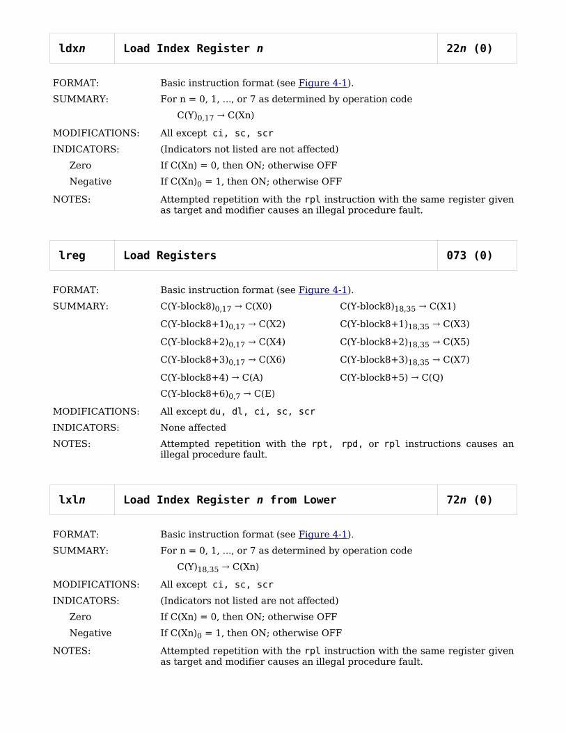
ldxn Load Index Register n 22n (0)
FORMAT: Basic instruction format (see Figure 4-1).
SUMMARY: For n = 0, 1, ..., or 7 as determined by operation code
C(Y)0,17 C(Xn)→
MODIFICATIONS: All except ci, sc, scr
INDICATORS: (Indicators not listed are not affected)
Zero If C(Xn) = 0, then ON; otherwise OFF
Negative If C(Xn)0 = 1, then ON; otherwise OFF
NOTES: Attempted repetition with the rpl instruction with the same register given as target and modifier causes an illegal procedure fault.
lreg Load Registers 073 (0)
FORMAT: Basic instruction format (see Figure 4-1).
SUMMARY: C(Y-block8)0,17 C(X0)→ C(Y-block8)18,35 C(X1)→
C(Y-block8+1)0,17 C(X2)→ C(Y-block8+1)18,35 C(X3)→
C(Y-block8+2)0,17 C(X4)→ C(Y-block8+2)18,35 C(X5)→
C(Y-block8+3)0,17 C(X6)→ C(Y-block8+3)18,35 C(X7)→
C(Y-block8+4) C(A)→ C(Y-block8+5) C(Q)→
C(Y-block8+6)0,7 C(E)→
MODIFICATIONS: All except du, dl, ci, sc, scr
INDICATORS: None affected
NOTES: Attempted repetition with the rpt, rpd, or rpl instructions causes an illegal procedure fault.
lxln Load Index Register n from Lower 72n (0)
FORMAT: Basic instruction format (see Figure 4-1).
SUMMARY: For n = 0, 1, ..., or 7 as determined by operation code
C(Y)18,35 C(Xn)→
MODIFICATIONS: All except ci, sc, scr
INDICATORS: (Indicators not listed are not affected)
Zero If C(Xn) = 0, then ON; otherwise OFF
Negative If C(Xn)0 = 1, then ON; otherwise OFF
NOTES: Attempted repetition with the rpl instruction with the same register given as target and modifier causes an illegal procedure fault.

Fixed-Point Data Movement Store
sreg Store Registers 753 (0)
FORMAT: Basic instruction format (see Figure 4-1).
SUMMARY: C(X0) C(Y-block8)→ 0,17 C(X1) C(Y-block8)→ 18,35
C(X2) C(Y-block8+1)→ 0,17 C(X3) C(Y-block8+1)→ 18,35
C(X4) C(Y-block8+2)→ 0,17 C(X5) C(Y-block8+2)→ 18,35
C(X6) C(Y-block8+3)→ 0,17 C(X7) C(Y-block8+3)→ 18,35
C(A) C(Y-block8+4)→ C(Q) C(Y-block8+5)→
C(E) C(Y-block8+6)→ 0,7 00...0 C(Y-block8+6)→ 8,35
C(TR) C(Y-block8+7)→ 0,26 00...0 C(Y-block8+7)→ 27,32
C(RALR) C(Y-block8+7)→ 33,35
MODIFICATIONS: All except du, dl, ci, sc, scr
INDICATORS: None affected
NOTES: Attempted repetition with the rpt, rpd, or rpl instructions causes an illegal procedure fault.
sta Store A 755 (0)
FORMAT: Basic instruction format (see Figure 4-1).
SUMMARY: C(A) C(Y)→
MODIFICATIONS: All except du, dl
INDICATORS: None affected
NOTES: Attempted repetition with the rpl instruction causes an illegal procedure fault.
stac Store A Conditional 354 (0)
FORMAT: Basic instruction format (see Figure 4-1).
SUMMARY: If C(Y) = 0, then C(A) C(Y)→
MODIFICATIONS: All except du, dl, ci, sc, scr
INDICATORS: (Indicators not listed are not affected)
Zero If initial C(Y) = 0, then ON; otherwise OFF
NOTES: If the initial C(Y) is nonzero, then C(Y) is not changed by the stac instruction.

The stac instruction uses a special main memory reference that prohibits such references by other processors between the test and the data transfer. Thus, it may be used for data locking.
Attempted repetition with the rpl instruction causes an illegal procedure fault.
stacq Store A Conditional on Q 654 (0)
FORMAT: Basic instruction format (see Figure 4-1).
SUMMARY: If C(Y) = C(Q), then C(A) C(Y)→
MODIFICATIONS: All except du, dl, ci, sc, scr
INDICATORS: (Indicators not listed are not affected)
Zero If initial C(Y) = C(Q), then ON; otherwise OFF
NOTES: If the initial C(Y) is ≠ C(Q), then C(Y) is not changed by the stacq instruction.
The stacq instruction uses a special main memory reference that prohibits such references by other processors between the test and the data transfer. Thus, it may be used for shared data locking and unlocking.
On the DPS 8M processor, data shared by more than one processor may, at any time, be in more than one processor's cache memory. To aid the integrity of shared data, the stacq instruction will always bypass cache and obtain its operand from main memory. In addition, a synchronizing function inhibits completion of the stacq instruction until the processor executing the stacq instruction is notified by the scu that write completes have occurred and write notifications requesting cache block clears have been sent to the other processors for all write instructions that the processor previously issued. This feature, therefore, makes the stacq instruction the preferred choice for unlocking shared data bases.
Attempted repetition with the rpl instruction causes an illegal procedure fault.
staq Store AQ 757 (0)
FORMAT: Basic instruction format (see Figure 4-1).
SUMMARY: C(AQ) C(Y-pair)→
MODIFICATIONS: All except du, dl, ci, sc, scr
INDICATORS: None affected
NOTES: Attempted repetition with the rpl instruction causes an illegal procedure fault.
stba Store Bytes of A 551 (0)
FORMAT: Basic instruction format (see Figure 4-1).
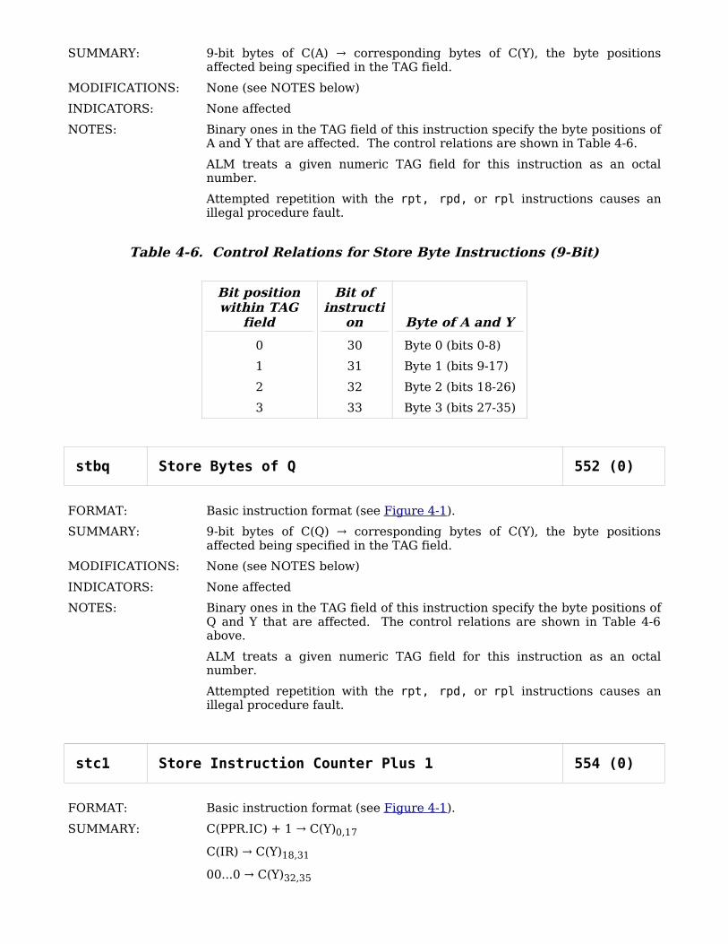
SUMMARY: 9-bit bytes of C(A) corresponding bytes of C(Y), the byte positions→ affected being specified in the TAG field.
MODIFICATIONS: None (see NOTES below)
INDICATORS: None affected
NOTES: Binary ones in the TAG field of this instruction specify the byte positions of A and Y that are affected. The control relations are shown in Table 4-6.
ALM treats a given numeric TAG field for this instruction as an octal number.
Attempted repetition with the rpt, rpd, or rpl instructions causes an illegal procedure fault.
Table 4-6. Control Relations for Store Byte Instructions (9-Bit)
Bit position within TAG
field
Bit of instructi
on Byte of A and Y
0 30 Byte 0 (bits 0-8)
1 31 Byte 1 (bits 9-17)
2 32 Byte 2 (bits 18-26)
3 33 Byte 3 (bits 27-35)
stbq Store Bytes of Q 552 (0)
FORMAT: Basic instruction format (see Figure 4-1).
SUMMARY: 9-bit bytes of C(Q) corresponding bytes of C(Y), the byte positions→ affected being specified in the TAG field.
MODIFICATIONS: None (see NOTES below)
INDICATORS: None affected
NOTES: Binary ones in the TAG field of this instruction specify the byte positions of Q and Y that are affected. The control relations are shown in Table 4-6 above.
ALM treats a given numeric TAG field for this instruction as an octal number.
Attempted repetition with the rpt, rpd, or rpl instructions causes an illegal procedure fault.
stc1 Store Instruction Counter Plus 1 554 (0)
FORMAT: Basic instruction format (see Figure 4-1).
SUMMARY: C(PPR.IC) + 1 C(Y)→ 0,17
C(IR) C(Y)→ 18,31
00...0 C(Y)→ 32,35
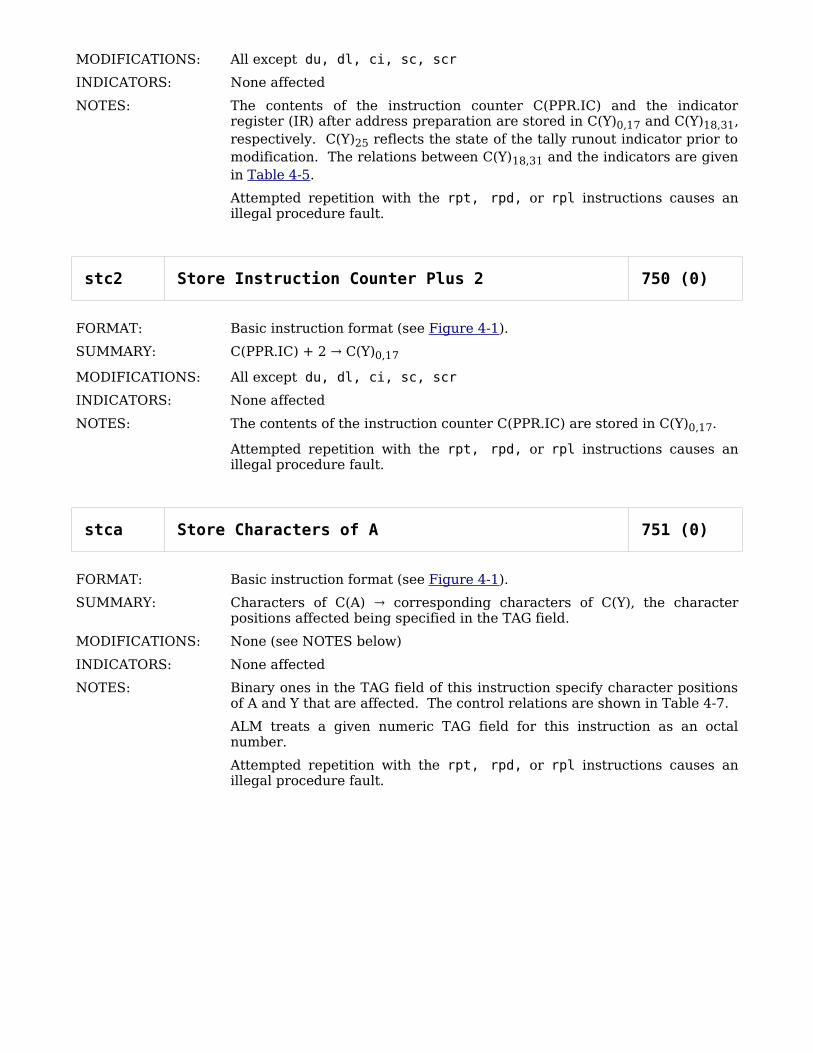
MODIFICATIONS: All except du, dl, ci, sc, scr
INDICATORS: None affected
NOTES: The contents of the instruction counter C(PPR.IC) and the indicator register (IR) after address preparation are stored in C(Y)0,17 and C(Y)18,31, respectively. C(Y)25 reflects the state of the tally runout indicator prior to modification. The relations between C(Y)18,31 and the indicators are given in Table 4-5.
Attempted repetition with the rpt, rpd, or rpl instructions causes an illegal procedure fault.
stc2 Store Instruction Counter Plus 2 750 (0)
FORMAT: Basic instruction format (see Figure 4-1).
SUMMARY: C(PPR.IC) + 2 C(Y)→ 0,17
MODIFICATIONS: All except du, dl, ci, sc, scr
INDICATORS: None affected
NOTES: The contents of the instruction counter C(PPR.IC) are stored in C(Y)0,17.
Attempted repetition with the rpt, rpd, or rpl instructions causes an illegal procedure fault.
stca Store Characters of A 751 (0)
FORMAT: Basic instruction format (see Figure 4-1).
SUMMARY: Characters of C(A) corresponding characters of C(Y), the character→ positions affected being specified in the TAG field.
MODIFICATIONS: None (see NOTES below)
INDICATORS: None affected
NOTES: Binary ones in the TAG field of this instruction specify character positions of A and Y that are affected. The control relations are shown in Table 4-7.
ALM treats a given numeric TAG field for this instruction as an octal number.
Attempted repetition with the rpt, rpd, or rpl instructions causes an illegal procedure fault.
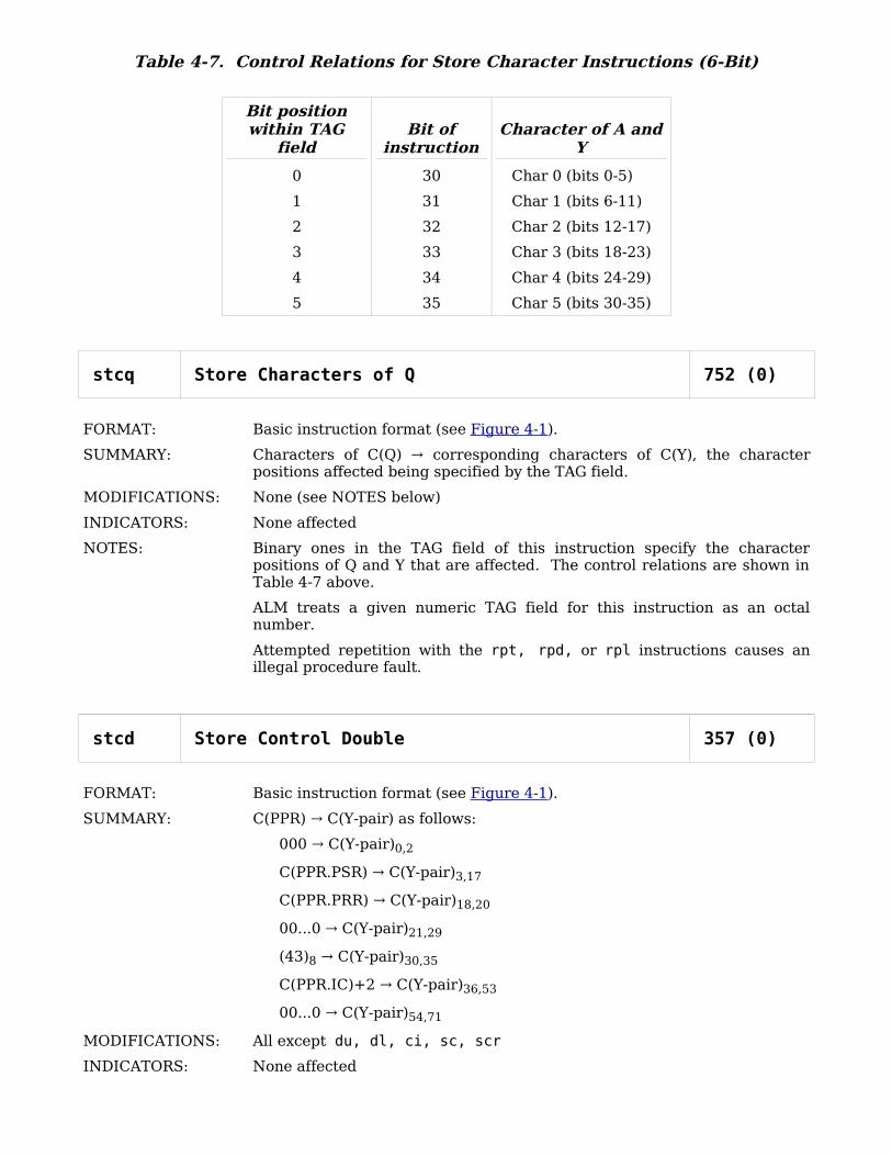
Table 4-7. Control Relations for Store Character Instructions (6-Bit)
Bit position within TAG
fieldBit of
instructionCharacter of A and
Y
0 30 Char 0 (bits 0-5)
1 31 Char 1 (bits 6-11)
2 32 Char 2 (bits 12-17)
3 33 Char 3 (bits 18-23)
4 34 Char 4 (bits 24-29)
5 35 Char 5 (bits 30-35)
stcq Store Characters of Q 752 (0)
FORMAT: Basic instruction format (see Figure 4-1).
SUMMARY: Characters of C(Q) corresponding characters of C(Y), the character→ positions affected being specified by the TAG field.
MODIFICATIONS: None (see NOTES below)
INDICATORS: None affected
NOTES: Binary ones in the TAG field of this instruction specify the character positions of Q and Y that are affected. The control relations are shown in Table 4-7 above.
ALM treats a given numeric TAG field for this instruction as an octal number.
Attempted repetition with the rpt, rpd, or rpl instructions causes an illegal procedure fault.
stcd Store Control Double 357 (0)
FORMAT: Basic instruction format (see Figure 4-1).
SUMMARY: C(PPR) C(Y-pair) as follows:→
000 C(Y-pair)→ 0,2
C(PPR.PSR) C(Y-pair)→ 3,17
C(PPR.PRR) C(Y-pair)→ 18,20
00...0 C(Y-pair)→ 21,29
(43)8 C(Y-pair)→ 30,35
C(PPR.IC)+2 C(Y-pair)→ 36,53
00...0 C(Y-pair)→ 54,71
MODIFICATIONS: All except du, dl, ci, sc, scr
INDICATORS: None affected

NOTES: Attempted repetition with the rpt, rpd, or rpl instructions causes an illegal procedure fault.
sti Store Indicator Register 754 (0)
FORMAT: Basic instruction format (see Figure 4-1).
SUMMARY: C(IR) C(Y)→ 18,31
00...0 C(Y)→ 32,35
MODIFICATIONS: All except du, dl, ci, sc, scr
INDICATORS: None affected
NOTES: The contents of the indicator register after address preparation are stored in C(Y)18,31. C(Y)18,31 reflects the state of the tally runout indicator prior to address preparation. The relation between C(Y)18,31 and the indicators is given in Table 4-5.
Attempted repetition with the rpt, rpd, or rpl instructions causes an illegal procedure fault.
stq Store Q 756 (0)
FORMAT: Basic instruction format (see Figure 4-1).
SUMMARY: C(Q) C(Y)→
MODIFICATIONS: All except du, dl
INDICATORS: None affected
NOTES: Attempted repetition with the rpl instruction causes an illegal procedure fault.
stt Store Timer Register 454 (0)
FORMAT: Basic instruction format (see Figure 4-1).
SUMMARY: C(TR) C(Y)→ 0,26
00...0 C(Y)→ 27,35
MODIFICATIONS: All except du, dl, ci, sc, scr
INDICATORS: None affected
NOTES: Attempted repetition with the rpt, rpd, or rpl instructions causes an illegal procedure fault.
stxn Store Index Register n 74n (0)
FORMAT: Basic instruction format (see Figure 4-1).
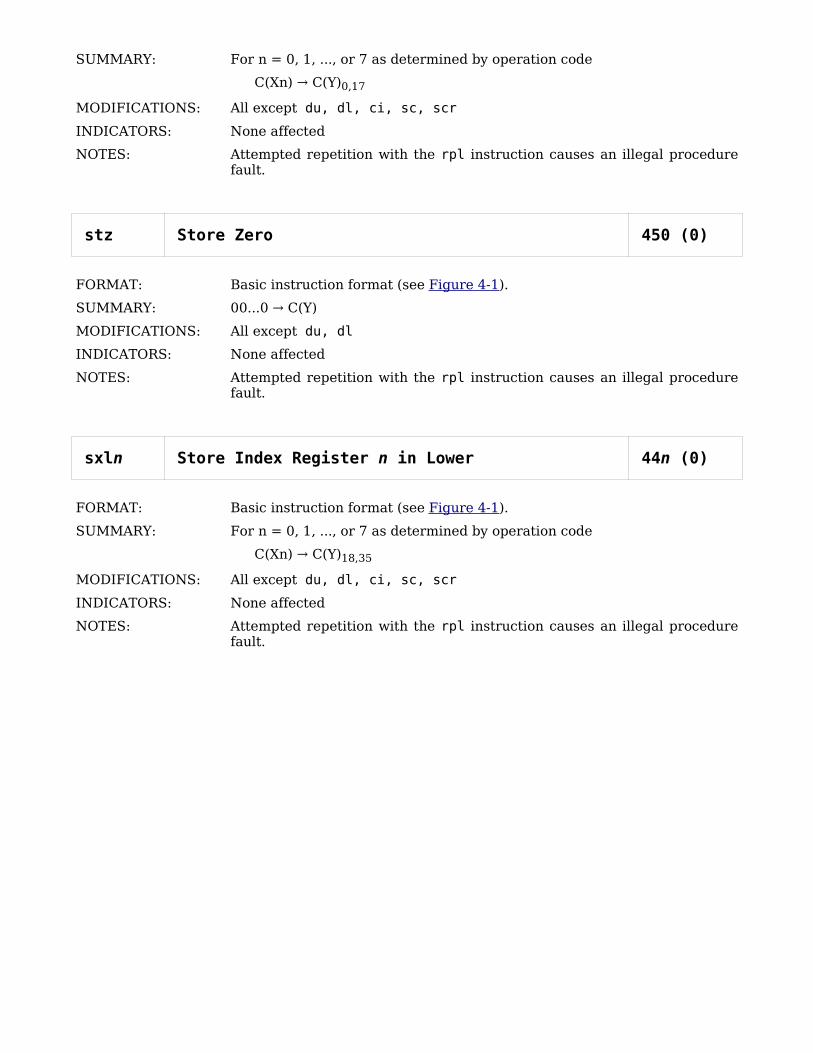
SUMMARY: For n = 0, 1, ..., or 7 as determined by operation code
C(Xn) C(Y)→ 0,17
MODIFICATIONS: All except du, dl, ci, sc, scr
INDICATORS: None affected
NOTES: Attempted repetition with the rpl instruction causes an illegal procedure fault.
stz Store Zero 450 (0)
FORMAT: Basic instruction format (see Figure 4-1).
SUMMARY: 00...0 C(Y)→
MODIFICATIONS: All except du, dl
INDICATORS: None affected
NOTES: Attempted repetition with the rpl instruction causes an illegal procedure fault.
sxln Store Index Register n in Lower 44n (0)
FORMAT: Basic instruction format (see Figure 4-1).
SUMMARY: For n = 0, 1, ..., or 7 as determined by operation code
C(Xn) C(Y)→ 18,35
MODIFICATIONS: All except du, dl, ci, sc, scr
INDICATORS: None affected
NOTES: Attempted repetition with the rpl instruction causes an illegal procedure fault.

Fixed-Point Data Movement Shift
alr A Left Rotate 775 (0)
FORMAT: Basic instruction format (see Figure 4-1).
SUMMARY: Shift C(A) left the number of positions given in C(TPR.CA)11,17; entering each bit leaving A0 into A35.
MODIFICATIONS: All except du, dl, ci, sc, scr
INDICATORS: (Indicators not listed are not affected)
Zero If C(A) = 0, then ON; otherwise OFF
Negative If C(A)0 = 1, then ON; otherwise OFF
NOTES: Attempted repetition with the rpl instruction causes an illegal procedure fault.
als A Left Shift 735 (0)
FORMAT: Basic instruction format (see Figure 4-1).
SUMMARY: Shift C(A) left the number of positions given in by C(TPR.CA)11,17; filling vacated positions with zeros.
MODIFICATIONS: All except du, dl, ci, sc, scr
INDICATORS: (Indicators not listed are not affected)
Zero If C(A) = 0, then ON; otherwise OFF
Negative If C(A)0 = 1, then ON; otherwise OFF
Carry If C(A)0 changes during the shift, then ON; otherwise OFF
NOTES: Attempted repetition with the rpl instruction causes an illegal procedure fault.
arl A Right Logical 771 (0)
FORMAT: Basic instruction format (see Figure 4-1).
SUMMARY: Shift C(A) right the number of positions given in C(TPR.CA)11,17; filling vacated positions with zeros.
MODIFICATIONS: All except du, dl, ci, sc, scr
INDICATORS: (Indicators not listed are not affected)
Zero If C(A) = 0, then ON; otherwise OFF
Negative If C(A)0 = 1, then ON; otherwise OFF
NOTES: Attempted repetition with the rpl instruction causes an illegal procedure fault.
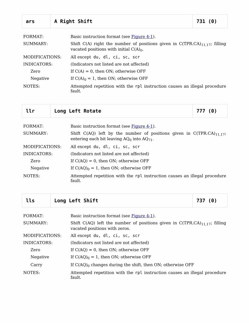
ars A Right Shift 731 (0)
FORMAT: Basic instruction format (see Figure 4-1).
SUMMARY: Shift C(A) right the number of positions given in C(TPR.CA)11,17; filling vacated positions with initial C(A)0.
MODIFICATIONS: All except du, dl, ci, sc, scr
INDICATORS: (Indicators not listed are not affected)
Zero If C(A) = 0, then ON; otherwise OFF
Negative If C(A)0 = 1, then ON; otherwise OFF
NOTES: Attempted repetition with the rpl instruction causes an illegal procedure fault.
llr Long Left Rotate 777 (0)
FORMAT: Basic instruction format (see Figure 4-1).
SUMMARY: Shift C(AQ) left by the number of positions given in C(TPR.CA)11,17; entering each bit leaving AQ0 into AQ71.
MODIFICATIONS: All except du, dl, ci, sc, scr
INDICATORS: (Indicators not listed are not affected)
Zero If C(AQ) = 0, then ON; otherwise OFF
Negative If C(AQ)0 = 1, then ON; otherwise OFF
NOTES: Attempted repetition with the rpl instruction causes an illegal procedure fault.
lls Long Left Shift 737 (0)
FORMAT: Basic instruction format (see Figure 4-1).
SUMMARY: Shift C(AQ) left the number of positions given in C(TPR.CA)11,17; filling vacated positions with zeros.
MODIFICATIONS: All except du, dl, ci, sc, scr
INDICATORS: (Indicators not listed are not affected)
Zero If C(AQ) = 0, then ON; otherwise OFF
Negative If C(AQ)0 = 1, then ON; otherwise OFF
Carry If C(AQ)0 changes during the shift, then ON; otherwise OFF
NOTES: Attempted repetition with the rpl instruction causes an illegal procedure fault.
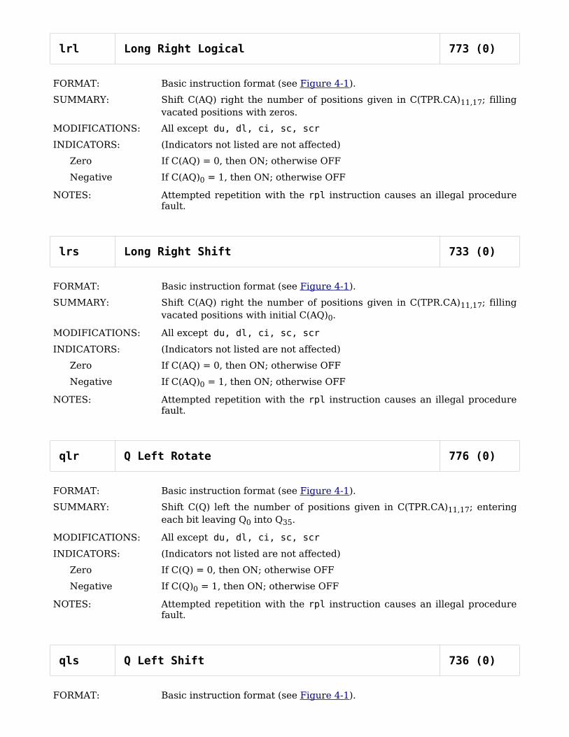
lrl Long Right Logical 773 (0)
FORMAT: Basic instruction format (see Figure 4-1).
SUMMARY: Shift C(AQ) right the number of positions given in C(TPR.CA)11,17; filling vacated positions with zeros.
MODIFICATIONS: All except du, dl, ci, sc, scr
INDICATORS: (Indicators not listed are not affected)
Zero If C(AQ) = 0, then ON; otherwise OFF
Negative If C(AQ)0 = 1, then ON; otherwise OFF
NOTES: Attempted repetition with the rpl instruction causes an illegal procedure fault.
lrs Long Right Shift 733 (0)
FORMAT: Basic instruction format (see Figure 4-1).
SUMMARY: Shift C(AQ) right the number of positions given in C(TPR.CA)11,17; filling vacated positions with initial C(AQ)0.
MODIFICATIONS: All except du, dl, ci, sc, scr
INDICATORS: (Indicators not listed are not affected)
Zero If C(AQ) = 0, then ON; otherwise OFF
Negative If C(AQ)0 = 1, then ON; otherwise OFF
NOTES: Attempted repetition with the rpl instruction causes an illegal procedure fault.
qlr Q Left Rotate 776 (0)
FORMAT: Basic instruction format (see Figure 4-1).
SUMMARY: Shift C(Q) left the number of positions given in C(TPR.CA)11,17; entering each bit leaving Q0 into Q35.
MODIFICATIONS: All except du, dl, ci, sc, scr
INDICATORS: (Indicators not listed are not affected)
Zero If C(Q) = 0, then ON; otherwise OFF
Negative If C(Q)0 = 1, then ON; otherwise OFF
NOTES: Attempted repetition with the rpl instruction causes an illegal procedure fault.
qls Q Left Shift 736 (0)
FORMAT: Basic instruction format (see Figure 4-1).
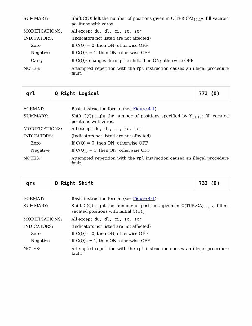
SUMMARY: Shift C(Q) left the number of positions given in C(TPR.CA)11,17; fill vacated positions with zeros.
MODIFICATIONS: All except du, dl, ci, sc, scr
INDICATORS: (Indicators not listed are not affected)
Zero If C(Q) = 0, then ON; otherwise OFF
Negative If C(Q)0 = 1, then ON; otherwise OFF
Carry If C(Q)0 changes during the shift, then ON; otherwise OFF
NOTES: Attempted repetition with the rpl instruction causes an illegal procedure fault.
qrl Q Right Logical 772 (0)
FORMAT: Basic instruction format (see Figure 4-1).
SUMMARY: Shift C(Q) right the number of positions specified by Y11,17; fill vacated positions with zeros.
MODIFICATIONS: All except du, dl, ci, sc, scr
INDICATORS: (Indicators not listed are not affected)
Zero If C(Q) = 0, then ON; otherwise OFF
Negative If C(Q)0 = 1, then ON; otherwise OFF
NOTES: Attempted repetition with the rpl instruction causes an illegal procedure fault.
qrs Q Right Shift 732 (0)
FORMAT: Basic instruction format (see Figure 4-1).
SUMMARY: Shift C(Q) right the number of positions given in C(TPR.CA)11,17; filling vacated positions with initial C(Q)0.
MODIFICATIONS: All except du, dl, ci, sc, scr
INDICATORS: (Indicators not listed are not affected)
Zero If C(Q) = 0, then ON; otherwise OFF
Negative If C(Q)0 = 1, then ON; otherwise OFF
NOTES: Attempted repetition with the rpl instruction causes an illegal procedure fault.

Fixed-Point Addition
ada Add to A 075 (0)
FORMAT: Basic instruction format (see Figure 4-1).
SUMMARY: C(A) + C(Y) C(A)→
MODIFICATIONS: All
INDICATORS: (Indicators not listed are not affected)
Zero If C(A) = 0, then ON; otherwise OFF
Negative If C(A)0 = 1, then ON; otherwise OFF
Overflow If range of A is exceeded, then ON
Carry If a carry out of A0 is generated, then ON; otherwise OFF
adaq Add to AQ 077 (0)
FORMAT: Basic instruction format (see Figure 4-1).
SUMMARY: C(AQ) + C(Y-pair) C(AQ)→
MODIFICATIONS: All except du, dl, ci, sc, scr
INDICATORS: (Indicators not listed are not affected)
Zero If C(AQ) = 0, then ON; otherwise OFF
Negative If C(AQ)0 = 1, then ON; otherwise OFF
Overflow If range of AQ is exceeded, then ON
Carry If a carry out of AQ0 is generated, then ON; otherwise OFF
adl Add Low to AQ 033 (0)
FORMAT: Basic instruction format (see Figure 4-1).
SUMMARY: C(AQ) + C(Y) sign extended C(AQ)→
MODIFICATIONS: All except ci, sc, scr
INDICATORS: (Indicators not listed are not affected)
Zero If C(AQ) = 0, then ON; otherwise OFF
Negative If C(AQ)0 = 1, then ON; otherwise OFF
Overflow If range of AQ is exceeded, then ON
Carry If a carry out of AQ0 is generated, then ON; otherwise OFF
NOTES: A 72-bit number is formed from C(Y) in the following manner:
The lower 36 bits (36,71) are identical to C(Y).Each of the upper 36 bits (0,35) is identical to C(Y)0.
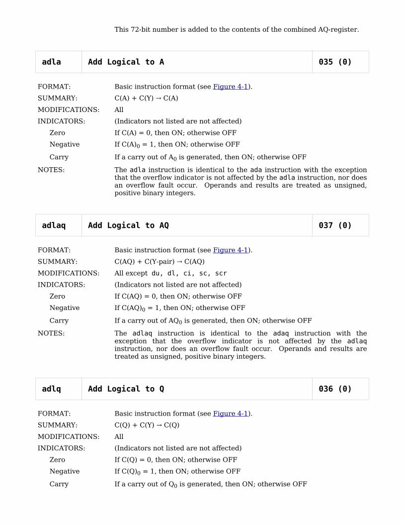
This 72-bit number is added to the contents of the combined AQ-register.
adla Add Logical to A 035 (0)
FORMAT: Basic instruction format (see Figure 4-1).
SUMMARY: C(A) + C(Y) C(A)→
MODIFICATIONS: All
INDICATORS: (Indicators not listed are not affected)
Zero If C(A) = 0, then ON; otherwise OFF
Negative If C(A)0 = 1, then ON; otherwise OFF
Carry If a carry out of A0 is generated, then ON; otherwise OFF
NOTES: The adla instruction is identical to the ada instruction with the exception that the overflow indicator is not affected by the adla instruction, nor does an overflow fault occur. Operands and results are treated as unsigned, positive binary integers.
adlaq Add Logical to AQ 037 (0)
FORMAT: Basic instruction format (see Figure 4-1).
SUMMARY: C(AQ) + C(Y-pair) C(AQ)→
MODIFICATIONS: All except du, dl, ci, sc, scr
INDICATORS: (Indicators not listed are not affected)
Zero If C(AQ) = 0, then ON; otherwise OFF
Negative If C(AQ)0 = 1, then ON; otherwise OFF
Carry If a carry out of AQ0 is generated, then ON; otherwise OFF
NOTES: The adlaq instruction is identical to the adaq instruction with the exception that the overflow indicator is not affected by the adlaq instruction, nor does an overflow fault occur. Operands and results are treated as unsigned, positive binary integers.
adlq Add Logical to Q 036 (0)
FORMAT: Basic instruction format (see Figure 4-1).
SUMMARY: C(Q) + C(Y) C(Q)→
MODIFICATIONS: All
INDICATORS: (Indicators not listed are not affected)
Zero If C(Q) = 0, then ON; otherwise OFF
Negative If C(Q)0 = 1, then ON; otherwise OFF
Carry If a carry out of Q0 is generated, then ON; otherwise OFF
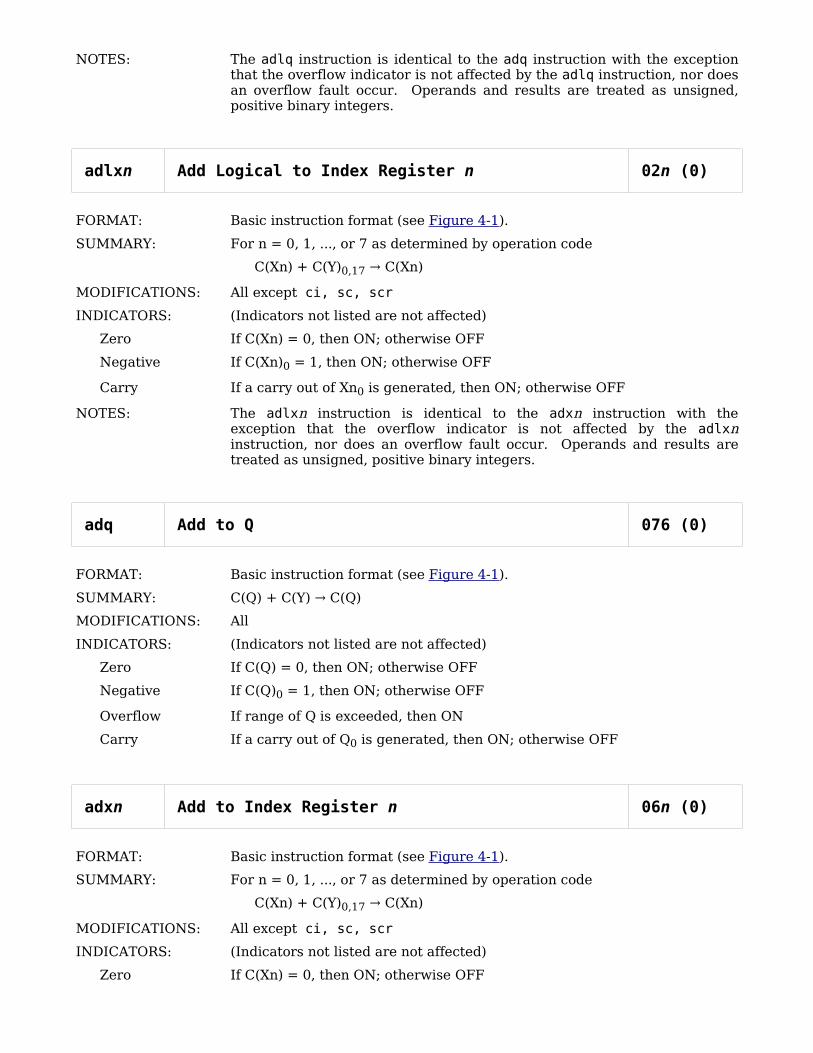
NOTES: The adlq instruction is identical to the adq instruction with the exception that the overflow indicator is not affected by the adlq instruction, nor does an overflow fault occur. Operands and results are treated as unsigned, positive binary integers.
adlxn Add Logical to Index Register n 02n (0)
FORMAT: Basic instruction format (see Figure 4-1).
SUMMARY: For n = 0, 1, ..., or 7 as determined by operation code
C(Xn) + C(Y)0,17 C(Xn)→
MODIFICATIONS: All except ci, sc, scr
INDICATORS: (Indicators not listed are not affected)
Zero If C(Xn) = 0, then ON; otherwise OFF
Negative If C(Xn)0 = 1, then ON; otherwise OFF
Carry If a carry out of Xn0 is generated, then ON; otherwise OFF
NOTES: The adlxn instruction is identical to the adxn instruction with the exception that the overflow indicator is not affected by the adlxn instruction, nor does an overflow fault occur. Operands and results are treated as unsigned, positive binary integers.
adq Add to Q 076 (0)
FORMAT: Basic instruction format (see Figure 4-1).
SUMMARY: C(Q) + C(Y) C(Q)→
MODIFICATIONS: All
INDICATORS: (Indicators not listed are not affected)
Zero If C(Q) = 0, then ON; otherwise OFF
Negative If C(Q)0 = 1, then ON; otherwise OFF
Overflow If range of Q is exceeded, then ON
Carry If a carry out of Q0 is generated, then ON; otherwise OFF
adxn Add to Index Register n 06n (0)
FORMAT: Basic instruction format (see Figure 4-1).
SUMMARY: For n = 0, 1, ..., or 7 as determined by operation code
C(Xn) + C(Y)0,17 C(Xn)→
MODIFICATIONS: All except ci, sc, scr
INDICATORS: (Indicators not listed are not affected)
Zero If C(Xn) = 0, then ON; otherwise OFF

Negative If C(Xn)0 = 1, then ON; otherwise OFF
Overflow If range of Xn is exceeded, then ON
Carry If a carry out of Xn0 is generated, then ON; otherwise OFF
aos Add One to Storage 054 (0)
FORMAT: Basic instruction format (see Figure 4-1).
SUMMARY: C(Y) + 1 C(Y)→
MODIFICATIONS: All except du, dl, ci, sc, scr
INDICATORS: (Indicators not listed are not affected)
Zero If C(Y) = 0, then ON; otherwise OFF
Negative If C(Y)0 = 1, then ON; otherwise OFF
Overflow If range of Y is exceeded, then ON
Carry If a carry out of Y0 is generated, then ON; otherwise OFF
NOTES: Attempted repetition with the rpl instruction causes an illegal procedure fault.
asa Add Stored to A 055 (0)
FORMAT: Basic instruction format (see Figure 4-1).
SUMMARY: C(A) + C(Y) C(Y)→
MODIFICATIONS: All except du, dl, ci, sc, scr
INDICATORS: (Indicators not listed are not affected)
Zero If C(Y) = 0, then ON; otherwise OFF
Negative If C(Y)0 = 1, then ON; otherwise OFF
Overflow If range of Y is exceeded, then ON
Carry If a carry out of Y0 is generated, then ON; otherwise OFF
NOTES: Attempted repetition with the rpl instruction causes an illegal procedure fault.
asq Add Stored to Q 056 (0)
FORMAT: Basic instruction format (see Figure 4-1).
SUMMARY: C(Q) + C(Y) C(Y)→
MODIFICATIONS: All except du, dl, ci, sc, scr
INDICATORS: (Indicators not listed are not affected)
Zero If C(Y) = 0, then ON; otherwise OFF
Negative IF C(Y)0 = 1, then ON; otherwise OFF

Overflow If range of Y is exceeded, then ON
Carry If a carry out of Y0 is generated, then ON; otherwise OFF
NOTES: Attempted repetition with the rpl instruction causes an illegal procedure fault.
asxn Add Stored to Index Register n 04n (0)
FORMAT: Basic instruction format (see Figure 4-1).
SUMMARY: For n = 0, 1, ..., or 7 as determined by operation code
C(Xn) + C(Y)0,17 C(Y)→ 0,17
MODIFICATIONS: All except du, dl, ci, sc, scr
INDICATORS: (Indicators not listed are not affected)
Zero If C(Y)0,17 = 0, then ON; otherwise OFF
Negative If C(Y)0 = 1, then ON; otherwise OFF
Overflow If range of Y0,17 is exceeded, then ON
Carry If a carry out of Y0 is generated, then ON; otherwise OFF
NOTES: Attempted repetition with the rpl instruction causes an illegal procedure fault.
awca Add with Carry to A 071 (0)
FORMAT: Basic instruction format (see Figure 4-1).
SUMMARY: If carry indicator OFF, then C(A) + C(Y) C(A)→
If carry indicator ON, then C(A) + C(Y) + 1 C(A)→
MODIFICATIONS: All
INDICATORS: (Indicators not listed are not affected)
Zero If C(A) = 0, then ON; otherwise OFF
Negative If C(A)0 = 1, then ON; otherwise OFF
Overflow If range of A is exceeded, then ON
Carry If a carry out of A0 is generated, then ON; otherwise OFF
NOTES: The awca instruction is identical to the ada instruction with the exception that when the carry indicator is ON at the beginning of the instruction, 1 is added to the sum of C(A) and C(Y).
awcq Add with Carry to Q 072 (0)
FORMAT: Basic instruction format (see Figure 4-1).
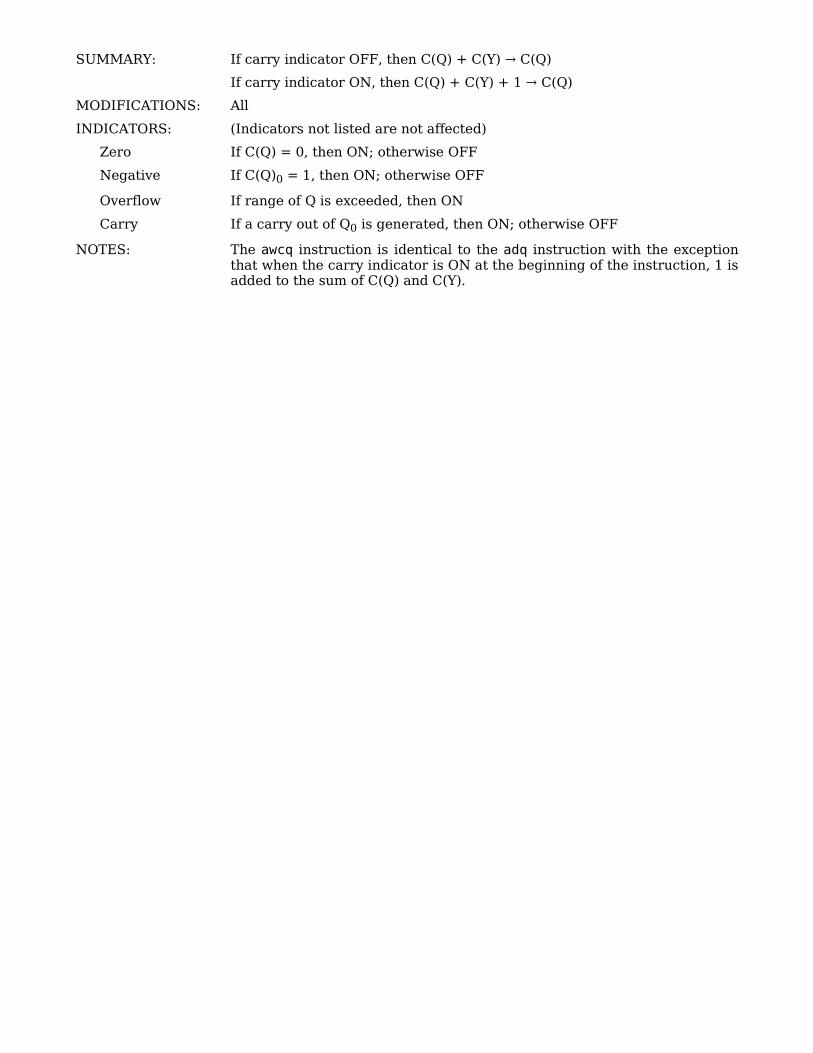
SUMMARY: If carry indicator OFF, then C(Q) + C(Y) C(Q)→
If carry indicator ON, then C(Q) + C(Y) + 1 C(Q)→
MODIFICATIONS: All
INDICATORS: (Indicators not listed are not affected)
Zero If C(Q) = 0, then ON; otherwise OFF
Negative If C(Q)0 = 1, then ON; otherwise OFF
Overflow If range of Q is exceeded, then ON
Carry If a carry out of Q0 is generated, then ON; otherwise OFF
NOTES: The awcq instruction is identical to the adq instruction with the exception that when the carry indicator is ON at the beginning of the instruction, 1 is added to the sum of C(Q) and C(Y).

Fixed-Point Subtraction
sba Subtract from A 175 (0)
FORMAT: Basic instruction format (see Figure 4-1).
SUMMARY: C(A) - C(Y) C(A)→
MODIFICATIONS: All
INDICATORS: (Indicators not listed are not affected)
Zero If C(A) = 0, then ON; otherwise OFF
Negative If C(A)0 = 1, then ON; otherwise OFF
Overflow If range of A is exceeded, then ON
Carry If a carry out of A0 is generated, then ON; otherwise OFF
sbaq Subtract from AQ 177 (0)
FORMAT: Basic instruction format (see Figure 4-1).
SUMMARY: C(AQ) - C(Y-pair) C(AQ)→
MODIFICATIONS: All except du, dl, ci, sc, scr
INDICATORS: (Indicators not listed are not affected)
Zero If C(AQ) = 0, then ON; otherwise OFF
Negative If C(AQ)0 = 1, then ON; otherwise OFF
Overflow If range of AQ is exceeded, then ON
Carry If a carry out of AQ0 is generated, then ON; otherwise OFF
sbla Subtract Logical from A 135 (0)
FORMAT: Basic instruction format (see Figure 4-1).
SUMMARY: C(A) - C(Y) C(A)→
MODIFICATIONS: All
INDICATORS: (Indicators not listed are not affected)
Zero If C(A) = 0, then ON; otherwise OFF
Negative If C(A)0 = 1, then ON; otherwise OFF
Carry If a carry out of A0 is generated, then ON; otherwise OFF
NOTES: The sbla instruction is identical to the sba instruction with the exception that the overflow indicator is not affected by the sbla instruction, nor does an overflow fault occur. Operands and results are treated as unsigned, positive binary integers.

sblaq Subtract Logical from AQ 137 (0)
FORMAT: Basic instruction format (see Figure 4-1).
SUMMARY: C(AQ) - C(Y-pair) C(AQ)→
MODIFICATIONS: All except du, dl, ci, sc, scr
INDICATORS: (Indicators not listed are not affected)
Zero If C(AQ) = 0, then ON; otherwise OFF
Negative If C(AQ)0 = 1, then ON; otherwise OFF
Carry If a carry out of AQ0 is generated, then ON; otherwise OFF
NOTES: The sblaq instruction is identical to the sbaq instruction with the exception that the overflow indicator is not affected by the sblaq instruction, nor does an overflow fault occur. Operands and results are treated as unsigned, positive binary integers.
sblq Subtract Logical from Q 136 (0)
FORMAT: Basic instruction format (see Figure 4-1).
SUMMARY: C(Q) - C(Y) C(Q)→
MODIFICATIONS: All
INDICATORS: (Indicators not listed are not affected)
Zero If C(Q) = 0, then ON; otherwise OFF
Negative If C(Q)0 = 1, then ON; otherwise OFF
Carry If a carry out of Q0 is generated, then ON; otherwise OFF
NOTES: The sblq instruction is identical to the sbq instruction with the exception that the overflow indicator is not affected by the sblq instruction, nor does an overflow fault occur. Operands and results are treated as unsigned, positive binary integers.
sblxn Subtract Logical from Index Register n 12n (0)
FORMAT: Basic instruction format (see Figure 4-1).
SUMMARY: For n = 0, 1, ..., or 7 as determined by operation code
C(Xn) - C(Y)0,17 C(Xn)→
MODIFICATIONS: All except ci, sc, scr
INDICATORS: (Indicators not listed are not affected)
Zero If C(Xn) = 0, then ON; otherwise OFF
Negative If C(Xn)0 = 1, then ON; otherwise OFF
Carry If a carry out of Xn0 is generated, then ON; otherwise OFF

NOTES The sblxn instruction is identical to the sbxn instruction with the exception that the overflow indicator is not affected by the sblxn instruction, nor does an overflow fault occur. Operands and results are treated as unsigned, positive binary integers.
sbq Subtract from Q 176 (0)
FORMAT: Basic instruction format (see Figure 4-1).
SUMMARY: C(Q) - C(Y) C(Q)→
MODIFICATIONS: All
INDICATORS: (Indicators not listed are not affected)
Zero If C(Q) = 0, then ON; otherwise OFF
Negative If C(Q)0 = 1, then ON; otherwise OFF
Overflow If range of Q is exceeded, then ON
Carry If a carry out of Q0 is generated, then ON; otherwise OFF
sbxn Subtract from Index Register n 16n (0)
FORMAT: Basic instruction format (see Figure 4-1).
SUMMARY: For n = 0, 1, ..., or 7 as determined by operation code
C(Xn) - C(Y)0,17 C(Xn)→
MODIFICATIONS: All except ci, sc, scr
INDICATORS: (Indicators not listed are not affected)
Zero If C(Xn) = 0, then ON; otherwise OFF
Negative If C(Xn)0 = 1, then ON; otherwise OFF
Overflow If range of Xn is exceeded, then ON
Carry If a carry out of Xn0 is generated, then ON; otherwise OFF
ssa Subtract Stored from A 155 (0)
FORMAT: Basic instruction format (see Figure 4-1).
SUMMARY: C(A) - C(Y) C(Y)→
MODIFICATIONS: All except du, dl, ci, sc, scr
INDICATORS: (Indicators not listed are not affected)
Zero If C(Y) = 0, then ON; otherwise OFF
Negative If C(Y)0 = 1, then ON; otherwise OFF
Overflow If range of Y is exceeded, then ON
Carry If a carry out of Y0 is generated, then ON; otherwise OFF

NOTES: Attempted repetition with the rpl instruction causes an illegal procedure fault.
ssq Subtract Stored from Q 156 (0)
FORMAT: Basic instruction format (see Figure 4-1).
SUMMARY: C(Q) - C(Y) C(Y)→
MODIFICATIONS: All except du, dl, ci, sc, scr
INDICATORS: (Indicators not listed are not affected)
Zero If C(Y) = 0, then ON; otherwise OFF
Negative If C(Y)0 = 1, then ON; otherwise OFF
Overflow If range of Y is exceeded, then ON
Carry If a carry out of Y0 is generated, then ON; otherwise OFF
NOTES: Attempted repetition with the rpl instruction causes an illegal procedure fault.
ssxn Subtract Stored from Index Register n 14n (0)
FORMAT: Basic instruction format (see Figure 4-1).
SUMMARY: For n = 0, 1, ..., or 7 as determined by operation code
C(Xn) - C(Y)0,17 C(Y)→ 0,17
MODIFICATIONS: All except du, dl, ci, sc, scr
INDICATORS: (Indicators not listed are not affected)
Zero If C(Y)0,17 = 0, then ON; otherwise OFF
Negative If C(Y)0 = 1, then ON; otherwise OFF
Overflow If range of Y0,17 exceeded, then ON
Carry If a carry out of Y0 is generated, then ON; otherwise OFF
NOTES: Attempted repetition with the rpl instruction causes an illegal procedure fault.
swca Subtract with Carry from A 171 (0)
FORMAT: Basic instruction format (see Figure 4-1).
SUMMARY: If carry indicator ON, then C(A)- C(Y) C(A)→
If carry indicator OFF, then C(A) - C(Y) - 1 C(A)→
MODIFICATIONS: All
INDICATORS: (Indicators not listed are not affected)
Zero If C(A) = 0, then ON; otherwise OFF
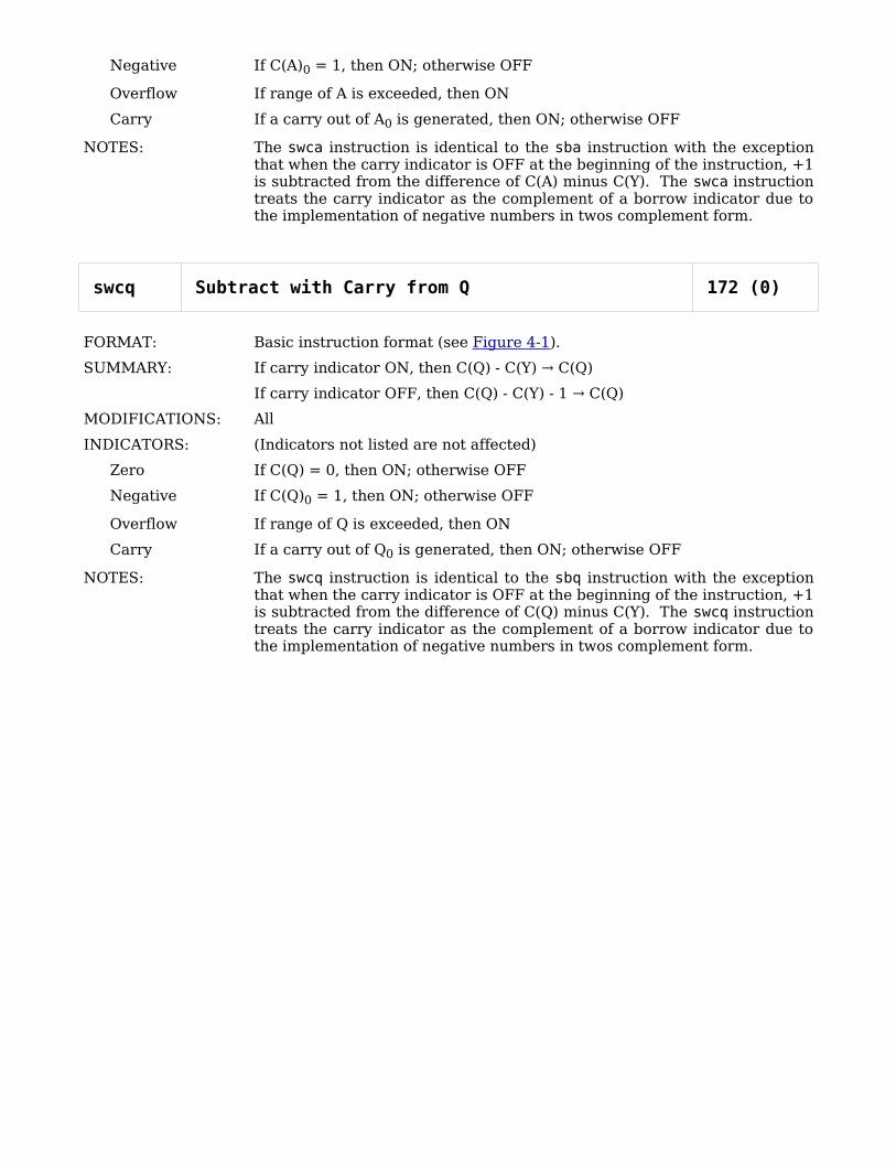
Negative If C(A)0 = 1, then ON; otherwise OFF
Overflow If range of A is exceeded, then ON
Carry If a carry out of A0 is generated, then ON; otherwise OFF
NOTES: The swca instruction is identical to the sba instruction with the exception that when the carry indicator is OFF at the beginning of the instruction, +1 is subtracted from the difference of C(A) minus C(Y). The swca instruction treats the carry indicator as the complement of a borrow indicator due to the implementation of negative numbers in twos complement form.
swcq Subtract with Carry from Q 172 (0)
FORMAT: Basic instruction format (see Figure 4-1).
SUMMARY: If carry indicator ON, then C(Q) - C(Y) C(Q)→
If carry indicator OFF, then C(Q) - C(Y) - 1 C(Q)→
MODIFICATIONS: All
INDICATORS: (Indicators not listed are not affected)
Zero If C(Q) = 0, then ON; otherwise OFF
Negative If C(Q)0 = 1, then ON; otherwise OFF
Overflow If range of Q is exceeded, then ON
Carry If a carry out of Q0 is generated, then ON; otherwise OFF
NOTES: The swcq instruction is identical to the sbq instruction with the exception that when the carry indicator is OFF at the beginning of the instruction, +1 is subtracted from the difference of C(Q) minus C(Y). The swcq instruction treats the carry indicator as the complement of a borrow indicator due to the implementation of negative numbers in twos complement form.
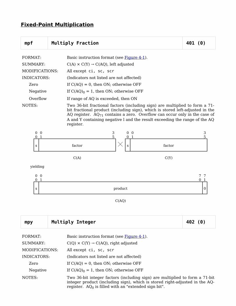
Fixed-Point Multiplication
mpf Multiply Fraction 401 (0)
FORMAT: Basic instruction format (see Figure 4-1).
SUMMARY: C(A) × C(Y) C(AQ), left adjusted→
MODIFICATIONS: All except ci, sc, scr
INDICATORS: (Indicators not listed are not affected)
Zero If C(AQ) = 0, then ON; otherwise OFF
Negative If C(AQ)0 = 1, then ON; otherwise OFF
Overflow If range of AQ is exceeded, then ON
NOTES: Two 36-bit fractional factors (including sign) are multiplied to form a 71-bit fractional product (including sign), which is stored left-adjusted in the AQ register. AQ71 contains a zero. Overflow can occur only in the case of A and Y containing negative l and the result exceeding the range of the AQ register.
mpy Multiply Integer 402 (0)
FORMAT: Basic instruction format (see Figure 4-1).
SUMMARY: C(Q) × C(Y) C(AQ), right adjusted→
MODIFICATIONS: All except ci, sc, scr
INDICATORS: (Indicators not listed are not affected)
Zero If C(AQ) = 0, then ON; otherwise OFF
Negative If C(AQ)0 = 1, then ON; otherwise OFF
NOTES: Two 36-bit integer factors (including sign) are multiplied to form a 71-bit integer product (including sign), which is stored right-adjusted in the AQ-register. AQ0 is filled with an "extended sign bit".
00
factor factor
35
ss
01
35
00
01
╳
C(A) C(Y)
yielding
s 0
00
01
71
product
C(AQ)
70
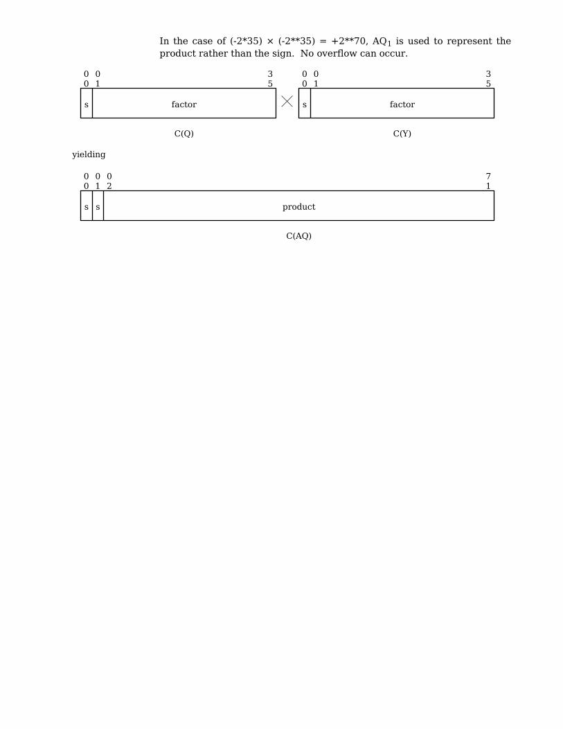
In the case of (-2*35) × (-2**35) = +2**70, AQ1 is used to represent the product rather than the sign. No overflow can occur.
00
factor factor
35
ss
01
35
00
01
╳
C(Q) C(Y)
yielding
s s
00
01
71
product
C(AQ)
02
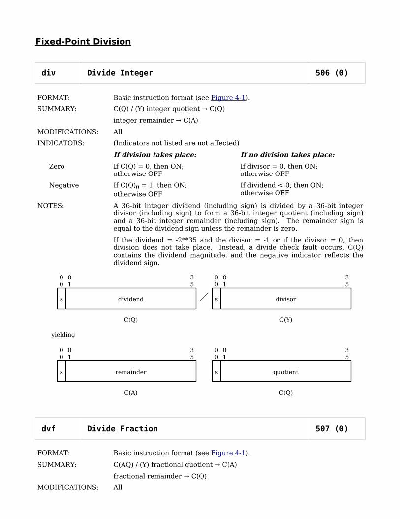
Fixed-Point Division
div Divide Integer 506 (0)
FORMAT: Basic instruction format (see Figure 4-1).
SUMMARY: C(Q) / (Y) integer quotient C(Q)→
integer remainder C(A)→
MODIFICATIONS: All
INDICATORS: (Indicators not listed are not affected)
If division takes place: If no division takes place:
Zero If C(Q) = 0, then ON;otherwise OFF
If divisor = 0, then ON;otherwise OFF
Negative If C(Q)0 = 1, then ON;otherwise OFF
If dividend < 0, then ON;otherwise OFF
NOTES: A 36-bit integer dividend (including sign) is divided by a 36-bit integer divisor (including sign) to form a 36-bit integer quotient (including sign) and a 36-bit integer remainder (including sign). The remainder sign is equal to the dividend sign unless the remainder is zero.
If the dividend = -2**35 and the divisor = -1 or if the divisor = 0, then division does not take place. Instead, a divide check fault occurs, C(Q) contains the dividend magnitude, and the negative indicator reflects the dividend sign.
dvf Divide Fraction 507 (0)
FORMAT: Basic instruction format (see Figure 4-1).
SUMMARY: C(AQ) / (Y) fractional quotient C(A)→
fractional remainder C(Q)→
MODIFICATIONS: All
s
00
dividend divisor
35
s
01
35
00
01
╱
C(Q) C(Y)
yielding
00
remainder quotient
35
s
01
35
00
01
C(A) C(Q)
s
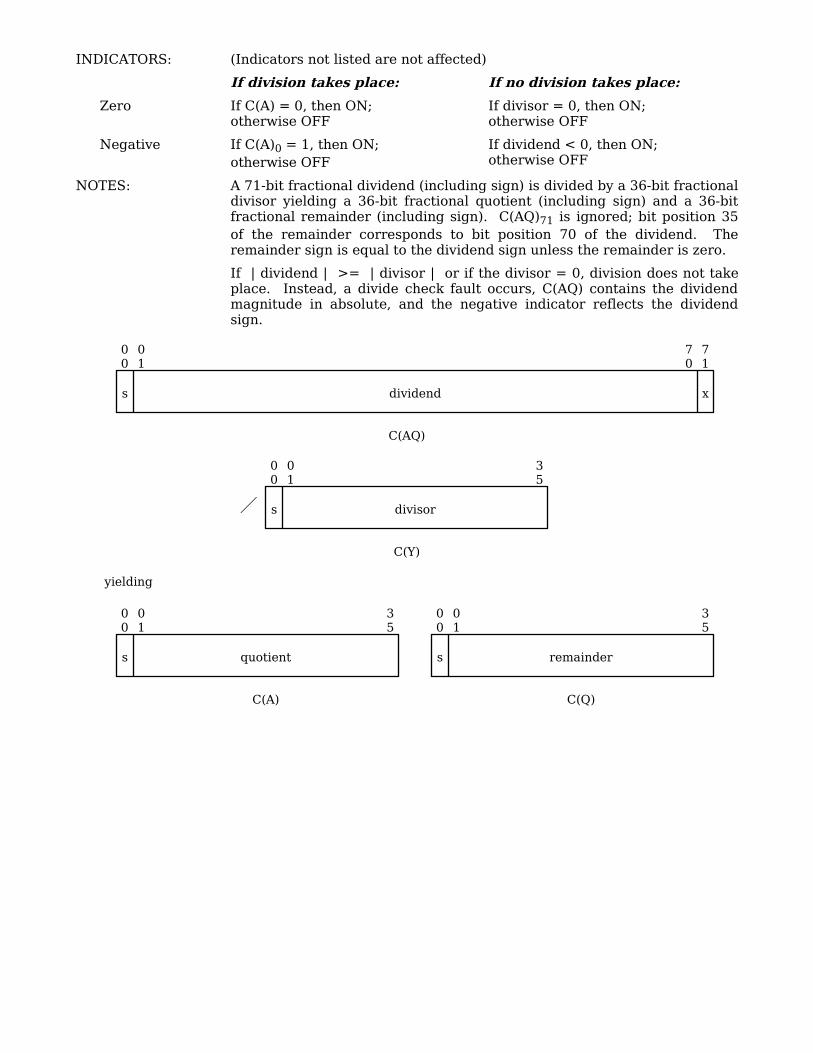
INDICATORS: (Indicators not listed are not affected)
If division takes place: If no division takes place:
Zero If C(A) = 0, then ON;otherwise OFF
If divisor = 0, then ON;otherwise OFF
Negative If C(A)0 = 1, then ON;otherwise OFF
If dividend < 0, then ON;otherwise OFF
NOTES: A 71-bit fractional dividend (including sign) is divided by a 36-bit fractional divisor yielding a 36-bit fractional quotient (including sign) and a 36-bit fractional remainder (including sign). C(AQ)71 is ignored; bit position 35 of the remainder corresponds to bit position 70 of the dividend. The remainder sign is equal to the dividend sign unless the remainder is zero.
If | dividend | >= | divisor | or if the divisor = 0, division does not take place. Instead, a divide check fault occurs, C(AQ) contains the dividend magnitude in absolute, and the negative indicator reflects the dividend sign.
divisor
35
s
00
01
╱
C(Y)
yielding
s
00
01
71
dividend
C(AQ)
70
x
00
quotient remainder
35
s
01
35
00
01
C(A) C(Q)
s
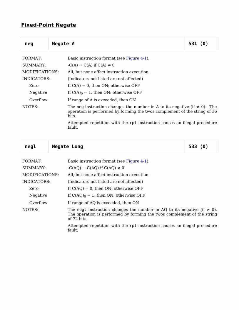
Fixed-Point Negate
neg Negate A 531 (0)
FORMAT: Basic instruction format (see Figure 4-1).
SUMMARY: -C(A) C(A) if C(A) ≠ 0→
MODIFICATIONS: All, but none affect instruction execution.
INDICATORS: (Indicators not listed are not affected)
Zero If C(A) = 0, then ON; otherwise OFF
Negative If C(A)0 = 1, then ON; otherwise OFF
Overflow If range of A is exceeded, then ON
NOTES: The neg instruction changes the number in A to its negative (if ≠ 0). The operation is performed by forming the twos complement of the string of 36 bits.
Attempted repetition with the rpl instruction causes an illegal procedure fault.
negl Negate Long 533 (0)
FORMAT: Basic instruction format (see Figure 4-1).
SUMMARY: -C(AQ) C(AQ) if C(AQ) ≠ 0→
MODIFICATIONS: All, but none affect instruction execution.
INDICATORS: (Indicators not listed are not affected)
Zero If C(AQ) = 0, then ON; otherwise OFF
Negative If C(AQ)0 = 1, then ON; otherwise OFF
Overflow If range of AQ is exceeded, then ON
NOTES: The negl instruction changes the number in AQ to its negative (if ≠ 0). The operation is performed by forming the twos complement of the string of 72 bits.
Attempted repetition with the rpl instruction causes an illegal procedure fault.
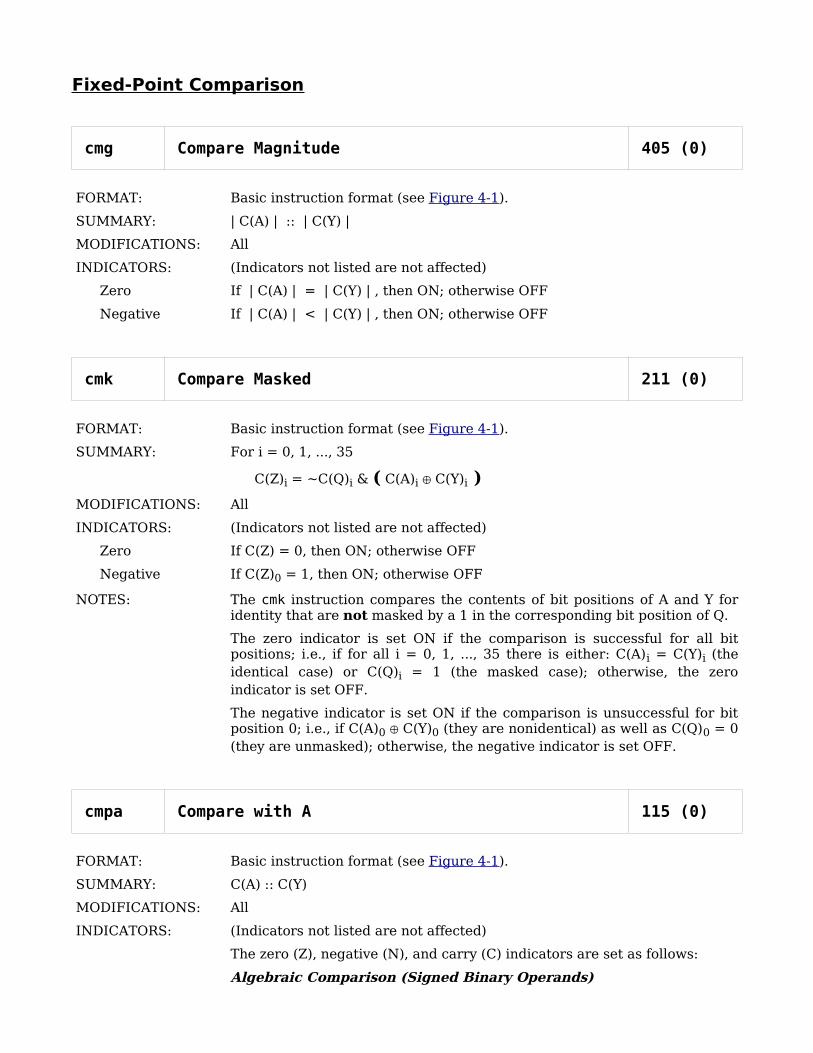
Fixed-Point Comparison
cmg Compare Magnitude 405 (0)
FORMAT: Basic instruction format (see Figure 4-1).
SUMMARY: | C(A) | :: | C(Y) |
MODIFICATIONS: All
INDICATORS: (Indicators not listed are not affected)
Zero If | C(A) | = | C(Y) | , then ON; otherwise OFF
Negative If | C(A) | < | C(Y) | , then ON; otherwise OFF
cmk Compare Masked 211 (0)
FORMAT: Basic instruction format (see Figure 4-1).
SUMMARY: For i = 0, 1, ..., 35
C(Z)i = ~C(Q)i & ( C(A)i C(Y)⊕ i )
MODIFICATIONS: All
INDICATORS: (Indicators not listed are not affected)
Zero If C(Z) = 0, then ON; otherwise OFF
Negative If C(Z)0 = 1, then ON; otherwise OFF
NOTES: The cmk instruction compares the contents of bit positions of A and Y for identity that are not masked by a 1 in the corresponding bit position of Q.
The zero indicator is set ON if the comparison is successful for all bit positions; i.e., if for all i = 0, 1, ..., 35 there is either: C(A)i = C(Y)i (the identical case) or C(Q)i = 1 (the masked case); otherwise, the zero indicator is set OFF.
The negative indicator is set ON if the comparison is unsuccessful for bit position 0; i.e., if C(A)0 C(Y)⊕ 0 (they are nonidentical) as well as C(Q)0 = 0 (they are unmasked); otherwise, the negative indicator is set OFF.
cmpa Compare with A 115 (0)
FORMAT: Basic instruction format (see Figure 4-1).
SUMMARY: C(A) :: C(Y)
MODIFICATIONS: All
INDICATORS: (Indicators not listed are not affected)
The zero (Z), negative (N), and carry (C) indicators are set as follows:
Algebraic Comparison (Signed Binary Operands)

Z N C Relation Sign
0 0 0 C(A) > C(Y) C(A)0 = 0, C(Y)0 = 1
0 0 1 C(A) > C(Y) C(A)0 = C(Y)0
1 0 1 C(A) = C(Y) C(A)0 = C(Y)0
0 1 0 C(A) < C(Y) C(A)0 = C(Y)0
0 1 1 C(A) < C(Y) C(A)0 = 1, C(Y)0 = 0
Logical Comparison (Unsigned Positive Binary Operands)
Z C Relation
0 0 C(A) < C(Y)
1 1 C(A) = C(Y)
0 1 C(A) > C(Y)
cmpaq Compare with AQ 117 (0)
FORMAT: Basic instruction format (see Figure 4-1).
SUMMARY: C(AQ) :: C(Y-pair)
MODIFICATIONS: All except du, dl, ci, sc, scr
INDICATORS: (Indicators not listed are not affected)
The zero (Z), negative (N), and carry (C) indicators are set as follows:
Algebraic Comparison (Signed Binary Operands)
Z N C Relation Sign
0 0 0 C(AQ) > C(Y-pair) C(AQ)0 = 0, C(Y-pair)0 = 1
0 0 1 C(AQ) > C(Y-pair) C(AQ)0 = C(Y-pair)0
1 0 1 C(AQ) = C(Y-pair) C(AQ)0 = C(Y-pair)0
0 1 0 C(AQ) < C(Y-pair) C(AQ)0 = C(Y-pair)0
0 1 1 C(AQ) < C(Y-pair) C(AQ)0 = 1, C(Y-pair)0 = Q
Logical Comparison (Unsigned Positive Binary Operands)
Z C Relation
0 0 C(AQ) < C(Y-pair)
1 1 C(AQ) = C(Y-pair)
0 1 C(AQ) > C(Y-pair)
cmpq Compare with Q 116 (0)
FORMAT: Basic instruction format (see Figure 4-1).
SUMMARY: C(Q) :: C(Y)
MODIFICATIONS: All
INDICATORS: (Indicators not listed are not affected)

The zero (Z), negative (N), and carry (C) indicators are set as follows:
Algebraic Comparison (Signed Binary Operands)
Z N C Relation Sign
0 0 0 C(Q) > C(Y) C(Q)0 = 0, C(Y)0 = 1
0 0 1 C(Q) > C(Y) C(Q)0 = C(Y)0
1 0 1 C(Q) = C(Y) C(Q)0 = C(Y)0
0 1 0 C(Q) < C(Y) C(Q)0 = C(Y)0
0 1 1 C(Q) < C(Y) C(Q)0 = 1, C(Y)0 = 0
Logical Comparison (Unsigned Positive Binary Operands)
Z C Relation
0 0 C(Q) < C(Y)
1 1 C(Q) = C(Y)
0 1 C(Q) > C(Y)
cmpxn Compare with Index Register n l0n (0)
FORMAT: Basic instruction format (see Figure 4-1).
SUMMARY: For n = 0, 1, ..., or 7 as determined by operation code
C(Xn) :: C(Y)0,17
MODIFICATIONS: All except ci, sc, scr
INDICATORS: (Indicators not listed are not affected)
The zero (Z), negative (N), and carry (C) indicators are set as follows:
Algebraic Comparison (Signed Binary Operands)
Z N C Relation Sign
0 0 0 C(Xn) > C(Y)0,17 C(Xn)0 = 0, C(Y)0 = 1
0 0 1 C(Xn) > C(Y)0,17 C(Xn)0 = C(Y)0
1 0 1 C(Xn) = C(Y)0,17 C(Xn)0 = C(Y)0
0 1 0 C(Xn) < C(Y)0,17 C(Xn)0 = C(Y)0
0 1 1 C(Xn) < C(Y)0,17 C(Xn)0 = 1, C(Y)0 = 0
Logical Comparison (Unsigned Positive Binary Operands)
Z C Relation
0 0 C(Xn) < C(Y)0,17
1 1 C(Xn) = C(Y)0,17
0 1 C(Xn) > C(Y)0,17

cwl Compare with Limits 111 (0)
FORMAT: Basic instruction format (see Figure 4-1).
SUMMARY: C(Y) :: closed interval [C(A);C(Q)]C(Y) :: C(Q)
MODIFICATIONS: All
INDICATORS: (Indicators not listed are not affected)
Zero If C(A) <= C(Y) <= C(Q) or C(A) >= C(Y) >= C(Q), then ON; otherwise OFF.
The negative (N) and carry (C) indicators are set as follows:
N C Relation Sign
0 0 C(Q) > C(Y) C(Q)0 = 0, C(Y)0 = 1
0 1 C(Q) >= C(Y) C(Q)0 = C(Y)0
1 0 C(Q) < C(Y) C(Q)0 = C(Y)0
1 1 C(Q) < C(Y) C(Q)0 = 1, C(Y)0 = Q
NOTES: The cwl instruction tests the value of C(Y) to determine if it is within the range of values set by C(A) and C(Q). The comparison of C(Y) with C(Q) locates C(Y) with respect to the interval if C(Y) is not contained within the interval.

Fixed-Point Miscellaneous
szn Set Zero and Negative Indicators 234 (0)
FORMAT: Basic instruction format (see Figure 4-1).
SUMMARY: Set indicators according to C(Y)
MODIFICATIONS: All
INDICATORS: (Indicators not listed are not affected)
Zero If C(Y) = 0, then ON; otherwise OFF
Negative If C(Y)0 = 1, then ON; otherwise OFF
sznc Set Zero and Negative Indicators and Clear 214 (0)
FORMAT: Basic instruction format (see Figure 4-1).
SUMMARY: Set indicators according to C(Y)
00...0 C(Y)→
MODIFICATIONS: All except du, dl, ci, sc, scr
INDICATORS: (Indicators not listed are not affected)
Zero If C(Y) = 0, then ON, otherwise OFF
Negative If C(Y)0 = 1, then ON; otherwise OFF
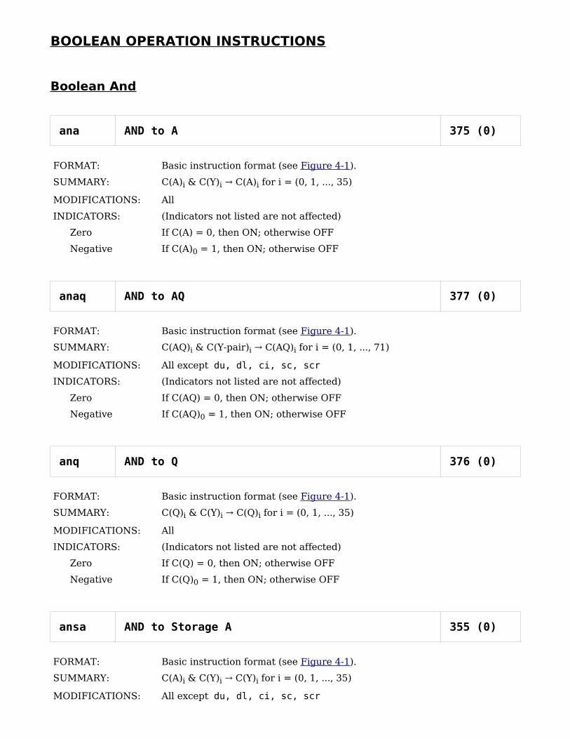
BOOLEAN OPERATION INSTRUCTIONS
Boolean And
ana AND to A 375 (0)
FORMAT: Basic instruction format (see Figure 4-1).
SUMMARY: C(A)i & C(Y)i C(A)→ i for i = (0, 1, ..., 35)
MODIFICATIONS: All
INDICATORS: (Indicators not listed are not affected)
Zero If C(A) = 0, then ON; otherwise OFF
Negative If C(A)0 = 1, then ON; otherwise OFF
anaq AND to AQ 377 (0)
FORMAT: Basic instruction format (see Figure 4-1).
SUMMARY: C(AQ)i & C(Y-pair)i C(AQ)→ i for i = (0, 1, ..., 71)
MODIFICATIONS: All except du, dl, ci, sc, scr
INDICATORS: (Indicators not listed are not affected)
Zero If C(AQ) = 0, then ON; otherwise OFF
Negative If C(AQ)0 = 1, then ON; otherwise OFF
anq AND to Q 376 (0)
FORMAT: Basic instruction format (see Figure 4-1).
SUMMARY: C(Q)i & C(Y)i C(Q)→ i for i = (0, 1, ..., 35)
MODIFICATIONS: All
INDICATORS: (Indicators not listed are not affected)
Zero If C(Q) = 0, then ON; otherwise OFF
Negative If C(Q)0 = 1, then ON; otherwise OFF
ansa AND to Storage A 355 (0)
FORMAT: Basic instruction format (see Figure 4-1).
SUMMARY: C(A)i & C(Y)i C(Y)→ i for i = (0, 1, ..., 35)
MODIFICATIONS: All except du, dl, ci, sc, scr

INDICATORS: (Indicators not listed are not affected)
Zero If C(Y) = 0, then ON; otherwise OFF
Negative If C(Y)0 = 1, then ON; otherwise OFF
NOTES: Attempted repetition with the rpl instruction causes an illegal procedure fault.
ansq AND to Storage Q 356 (0)
FORMAT: Basic instruction format (see Figure 4-1).
SUMMARY: C(Q)i & C(Y)i C(Y)→ i for i = (0, 1, ..., 35)
MODIFICATIONS: All except du, dl, ci, sc, scr
INDICATORS: (Indicators not listed are not affected)
Zero If C(Y) = 0, then ON; otherwise OFF
Negative If C(Y)0 = 1, then ON; otherwise OFF
NOTES: Attempted repetition with the rpl instruction causes an illegal procedure fault.
ansxn AND to Storage Index Register n 34n (0)
FORMAT: Basic instruction format (see Figure 4-1).
SUMMARY: For n = 0, 1, ..., or 7 as determined by operation code
C(Xn)i & C(Y)i C(Y)→ i for i = (0, 1, ..., 17)
MODIFICATIONS: All except du, dl, ci, sc, scr
INDICATORS: (Indicators not listed are not affected)
Zero If C(Y)0,17 = 0, then ON; otherwise OFF
Negative If C(Y)0 = 1, then ON; otherwise OFF
NOTES: Attempted repetition with the rpl instruction causes an illegal procedure fault.
anxn AND to Index Register n 36n (0)
FORMAT: Basic instruction format (see Figure 4-1).
SUMMARY: For n = 0, 1, ..., or 7 as determined by operation code
C(Xn)i & C(Y)i C(Xn)→ i for i = (0, 1, ..., 17)
MODIFICATIONS: All except ci, sc, scr
INDICATORS: (Indicators not listed are not affected)
Zero If C(Xn) = 0, then ON; otherwise OFF
Negative If C(Xn)0 = 1, then ON; otherwise OFF

Boolean Or
ora OR to A 275 (0)
FORMAT: Basic instruction format (see Figure 4-1).
SUMMARY: C(A)i | C(Y)i C(A)→ i for i = (0, 1, ..., 35)
MODIFICATIONS: All
INDICATORS: (Indicators not listed are not affected)
Zero If C(A) = 0, then ON; otherwise OFF
Negative If C(A)0 = 1, then ON; otherwise OFF
oraq OR to AQ 277 (0)
FORMAT: Basic instruction format (see Figure 4-1).
SUMMARY: C(AQ)i | C(Y-pair)i C(AQ)→ i for i = (0, 1, ..., 71)
MODIFICATIONS: All except du, dl, ci, sc, scr
INDICATORS: (Indicators not listed are not affected)
Zero If C(AQ) = 0, then ON; otherwise OFF
Negative If C(AQ)0 = 1, then ON; otherwise OFF
orq OR to Q 276 (0)
FORMAT: Basic instruction format (see Figure 4-1).
SUMMARY: C(Q)i | C(Y)i C(Q)→ i for i = (0, 1, ..., 35)
MODIFICATIONS: All
INDICATORS: (Indicators not listed are not affected)
Zero If C(Q) = 0, then ON; otherwise OFF
Negative If C(Q)0 = 1, then ON; otherwise OFF
orsa OR to Storage A 255 (0)
FORMAT: Basic instruction format (see Figure 4-1).
SUMMARY: C(A)i | C(Y)i C(Y)→ i for i = (0, 1, ..., 35)
MODIFICATIONS: All except du, dl, ci, sc, scr
INDICATORS: (Indicators not listed are not affected)
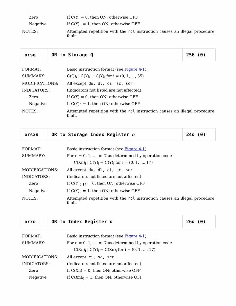
Zero If C(Y) = 0, then ON; otherwise OFF
Negative If C(Y)0 = 1, then ON; otherwise OFF
NOTES: Attempted repetition with the rpl instruction causes an illegal procedure fault.
orsq OR to Storage Q 256 (0)
FORMAT: Basic instruction format (see Figure 4-1).
SUMMARY: C(Q)i | C(Y)i C(Y)→ i for i = (0, 1, ..., 35)
MODIFICATIONS: All except du, dl, ci, sc, scr
INDICATORS: (Indicators not listed are not affected)
Zero If C(Y) = 0, then ON; otherwise OFF
Negative If C(Y)0 = 1, then ON; otherwise OFF
NOTES: Attempted repetition with the rpl instruction causes an illegal procedure fault.
orsxn OR to Storage Index Register n 24n (0)
FORMAT: Basic instruction format (see Figure 4-1).
SUMMARY: For n = 0, 1, ..., or 7 as determined by operation code
C(Xn)i | C(Y)i C(Y)→ i for i = (0, 1, ..., 17)
MODIFICATIONS: All except du, dl, ci, sc, scr
INDICATORS: (Indicators not listed are not affected)
Zero If C(Y)0,17 = 0, then ON; otherwise OFF
Negative If C(Y)0 = 1, then ON; otherwise OFF
NOTES: Attempted repetition with the rpl instruction causes an illegal procedure fault.
orxn OR to Index Register n 26n (0)
FORMAT: Basic instruction format (see Figure 4-1).
SUMMARY: For n = 0, 1, ..., or 7 as determined by operation code
C(Xn)i | C(Y)i C(Xn)→ i for i = (0, 1, ..., 17)
MODIFICATIONS: All except ci, sc, scr
INDICATORS: (Indicators not listed are not affected)
Zero If C(Xn) = 0, then ON; otherwise OFF
Negative If C(Xn)0 = 1, then ON; otherwise OFF
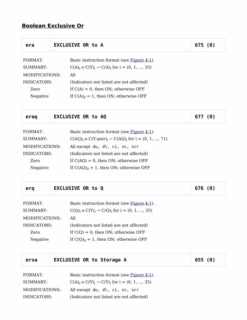
Boolean Exclusive Or
era EXCLUSIVE OR to A 675 (0)
FORMAT: Basic instruction format (see Figure 4-1).
SUMMARY: C(A)i C(Y)⊕ i C(A)→ i for i = (0, 1, ..., 35)
MODIFICATIONS: All
INDICATORS: (Indicators not listed are not affected)
Zero If C(A) = 0, then ON; otherwise OFF
Negative If C(A)0 = 1, then ON; otherwise OFF
eraq EXCLUSIVE OR to AQ 677 (0)
FORMAT: Basic instruction format (see Figure 4-1).
SUMMARY: C(AQ)i C(Y-pair)⊕ i C(AQ)→ i for i = (0, 1, ..., 71)
MODIFICATIONS: All except du, dl, ci, sc, scr
INDICATORS: (Indicators not listed are not affected)
Zero If C(AQ) = 0, then ON; otherwise OFF
Negative If C(AQ)0 = 1, then ON; otherwise OFF
erq EXCLUSIVE OR to Q 676 (0)
FORMAT: Basic instruction format (see Figure 4-1).
SUMMARY: C(Q)i C(Y)⊕ i C(Q)→ i for i = (0, 1, ..., 35)
MODIFICATIONS: All
INDICATORS: (Indicators not listed are not affected)
Zero If C(Q) = 0, then ON; otherwise OFF
Negative If C(Q)0 = 1, then ON; otherwise OFF
ersa EXCLUSIVE OR to Storage A 655 (0)
FORMAT: Basic instruction format (see Figure 4-1).
SUMMARY: C(A)i C(Y)⊕ i C(Y)→ i for i = (0, 1, ..., 35)
MODIFICATIONS: All except du, dl, ci, sc, scr
INDICATORS: (Indicators not listed are not affected)

Zero If C(Y) = 0, then ON; otherwise OFF
Negative If C(Y)0 = 1, then ON; otherwise OFF
NOTES: Attempted repetition with the rpl instruction causes an illegal procedure fault.
ersq EXCLUSIVE OR to Storage Q 656 (0)
FORMAT: Basic instruction format (see Figure 4-1).
SUMMARY: C(Q)i C(Y)⊕ i C(Y)→ i for i = (0, 1, ..., 35)
MODIFICATIONS: All except du, dl, ci, sc, scr
INDICATORS: (Indicators not listed are not affected)
Zero If C(Y) = 0, then ON; otherwise OFF
Negative If C(Y)0 = 1, then ON; otherwise OFF
NOTES: Attempted repetition with the rpl instruction causes an illegal procedure fault.
ersxn EXCLUSIVE OR to Storage Index Register n 64n (0)
FORMAT: Basic instruction format (see Figure 4-1).
SUMMARY: For n = 0, 1, ..., or 7 as determined by operation code
C(Xn)i C(Y)⊕ i C(Y)→ i for i = (0, 1, ..., 17)
MODIFICATIONS: All except du, dl, ci, sc, scr
INDICATORS: (Indicators not listed are not affected)
Zero If C(Y)0,17 = 0, then ON; otherwise OFF
Negative If C(Y)0 = 0, then ON; otherwise OFF
NOTES: Attempted repetition with the rpl instruction causes an illegal procedure fault.
erxn EXCLUSIVE OR to Index Register n 66n (0)
FORMAT: Basic instruction format (see Figure 4-1).
SUMMARY: For n = 0, 1, ..., or 7 as determined by operation code
C(Xn)i C(Y)⊕ i C(Xn)→ i for i = (0, 1, ..., 17)
MODIFICATIONS: All except ci, sc, scr
INDICATORS: (Indicators not listed are not affected)
Zero If C(Xn) = 0, then ON; otherwise OFF
Negative If C(Xn)0 = 1, then ON; otherwise OFF

Boolean Comparative And
cana Comparative AND with A 315 (0)
FORMAT: Basic instruction format (see Figure 4-1).
SUMMARY: C(Z)i = C(A)i & C(Y)i for i = (0, 1, ..., 35)
MODIFICATIONS: All
INDICATORS: (Indicators not listed are not affected)
Zero If C(Z) = 0, then ON; otherwise OFF
Negative If C(Z)0 = 1, then ON; otherwise OFF
canaq Comparative AND with AQ 317 (0)
FORMAT: Basic instruction format (see Figure 4-1).
SUMMARY: C(Z)i = C(AQ)i & C(Y-pair)i for i = (0, 1, ..., 71)
MODIFICATIONS: All except du, dl, ci, sc, scr
INDICATORS: (Indicators not listed are not affected)
Zero If C(Z) = 0, then ON; otherwise OFF
Negative If C(Z)0 = 1, then ON; otherwise OFF
canq Comparative AND with Q 316 (0)
FORMAT: Basic instruction format (see Figure 4-1).
SUMMARY: C(Z)i = C(Q)i & C(Y)i for i = (0, 1, ..., 35)
MODIFICATIONS: All
INDICATORS: (Indicators not listed are not affected)
Zero If C(Z) = 0, then ON; otherwise OFF
Negative If C(Z)0 = 1, then ON; otherwise OFF
canxn Comparative AND with Index Register n 30n (0)
FORMAT: Basic instruction format (see Figure 4-1).
SUMMARY: For n = 0, 1, ..., or 7 as determined by operation code
C(Z)i = C(Xn)i & C(Y)i for i = (0, 1, ..., 17)
MODIFICATIONS: All except ci, sc, scr

INDICATORS: (Indicators not listed are not affected)
Zero If C(Z) = 0, then ON; otherwise OFF
Negative If C(Z)0 = 1, then ON; otherwise OFF

Boolean Comparative Not
cnaa Comparative NOT with A 215 (0)
FORMAT: Basic instruction format (see Figure 4-1).
SUMMARY: C(Z)i = C(A)i & ~C(Y)i for i = (0, 1, ..., 35)
MODIFICATIONS: All
INDICATORS: (Indicators not listed are not affected)
Zero If C(Z) = 0, then ON; otherwise OFF
Negative If C(Z)0 = 1, then ON; otherwise OFF
cnaaq Comparative NOT with AQ 217 (0)
FORMAT: Basic instruction format (see Figure 4-1).
SUMMARY: C(Z)i = C (AQ)i & ~C(Y-pair)i for i = (0, 1, ..., 71)
MODIFICATIONS: All except du, dl, ci, sc, scr
INDICATORS: (Indicators not listed are not affected)
Zero If C(Z) = 0, then ON; otherwise OFF
Negative If C(Z)0 = 1, then ON; otherwise OFF
cnaq Comparative NOT with Q 216 (0)
FORMAT: Basic instruction format (see Figure 4-1).
SUMMARY: C(Z)i = C(Q)i & ~C(Y)i for i = (0, 1, ..., 35)
MODIFICATIONS: All
INDICATORS: (Indicators not listed are not affected)
Zero If C(Z) = 0, then ON; otherwise OFF
Negative If C(Z)0 = 1, then ON; otherwise OFF
cnaxn Comparative NOT with Index Register n 20n (0)
FORMAT: Basic instruction format (see Figure 4-1).
SUMMARY: For n = 0, 1, ..., or 7 as determined by operation code
C(Z)i = C(Xn)i & ~C(Y)i for i = (0, 1, ..., 17)

MODIFICATIONS: All except ci, sc, scr
INDICATORS: (Indicators not listed are not affected)
Zero If C(Z) = 0, then ON; otherwise OFF
Negative If C(Z)0 = 1, then ON; otherwise OFF

FLOATING-POINT ARITHMETIC INSTRUCTIONS
Floating-Point Data Movement Load
dfld Double-Precision Floating Load 433 (0)
FORMAT: Basic instruction format (see Figure 4-1).
SUMMARY: C(Y-pair)0,7 C(E)→
C(Y-pair)8,71 C(AQ)→ 0,63
00...0 C(AQ)→ 64,71
MODIFICATIONS: All except du, dl, ci, sc, scr
INDICATORS: (Indicators not listed are not affected)
Zero If C(AQ) = 0, then ON; otherwise OFF
Negative If C(AQ)0 = 1, then ON; otherwise OFF
fld Floating Load 431 (0)
FORMAT: Basic instruction format (see Figure 4-1).
SUMMARY: C(Y)0,7 C(E)→
C(Y)8,35 C(AQ)→ 0,27
00...0 C(AQ)→ 30,71
MODIFICATIONS: All except ci, sc, scr
INDICATORS: (Indicators not listed are not affected)
Zero If C(AQ) = 0, then ON; otherwise OFF
Negative If C(AQ)0 = 1, then ON; otherwise OFF

Floating-Point Data Movement Store
dfst Double-Precision Floating Store 457 (0)
FORMAT: Basic instruction format (see Figure 4-1).
SUMMARY: C(E) C(Y-pair)→ 0,7
C(AQ)0,63 C(Y-pair)→ 8,71
MODIFICATIONS: All except du, dl, ci, sc, scr
INDICATORS: None affected
NOTES: Attempted repetition with the rpl instruction causes an illegal procedure fault.
dfstr Double-Precision Floating Store Rounded 472 (0)
FORMAT: Basic instruction format (see Figure 4-1).
SUMMARY: C(EAQ) rounded C(Y-pair) (as in → dfst)
MODIFICATIONS: All except du, dl, ci, sc, scr
INDICATORS: (Indicators not listed are not affected)
Zero If C(Y-pair) = floating point 0, then ON; otherwise OFF
Negative If C(Y-pair)8 = 1, then ON; otherwise OFF
Exponent Overflow
If exponent is greater than +127, then ON
Exponent Underflow
If exponent is less than -128, then ON
NOTES: The dfstr instruction performs a double-precision true round and normalization on C(EAQ) as it is stored.
The definition of true round is located under the description of the frd instruction.
The definition of normalization is located under the description of the fno instruction.
Except for the precision of the stored result, the dfstr instruction is identical to the fstr instruction.
Attempted repetition with the rpl instruction causes an illegal procedure fault.
fst Floating Store 455 (0)
FORMAT: Basic instruction format (see Figure 4-1).

SUMMARY: C(E) C(Y)→ 0,7
C(A)0,27 C(Y)→ 8,35
MODIFICATIONS: All except du, dl, ci, sc, scr
INDICATORS: None affected
NOTES: Attempted repetition with the rpl instruction causes an illegal procedure fault.
fstr Floating Store Rounded 470 (0)
FORMAT: Basic instruction format (see Figure 4-1).
SUMMARY: C(EAQ) rounded C(Y) (as in → fst)
MODIFICATIONS: All except du, dl, ci, sc, scr
INDICATORS: (Indicators not listed are not affected)
Zero If C(Y) = floating point 0, then ON; otherwise OFF
Negative If C(Y)8 = 1, then ON; otherwise OFF
Exponent Overflow
If exponent is greater than +127, then ON
Exponent Underflow
If exponent is less than -128, then ON
NOTES: The fstr instruction performs a true round and normalization on C(EAQ) as it is stored.
The definition of true round is located under the description of the frd instruction.
The definition of normalization is located under the description of the fno instruction.
Attempted repetition with the rpl instruction causes an illegal procedure fault.

Floating-Point Addition
dfad Double-Precision Floating Add 477 (0)
FORMAT: Basic instruction format (see Figure 4-1).
SUMMARY: ( C(EAQ) + C(Y-pair) ) normalized C(EAQ)→
MODIFICATIONS: All except du, dl, ci, sc, scr
INDICATORS: (Indicators not listed are not affected)
Zero If C(AQ) = 0, then ON; otherwise OFF
Negative If C(AQ)0 = 1, then ON; otherwise OFF
Exponent Overflow
If exponent is greater than +127, then ON
Exponent Underflow
If exponent is less than -128, then ON
Carry If a carry out of AQ0 is generated, then ON; otherwise OFF
NOTES: The dfad instruction may be thought of as a dufa instruction followed by a fno instruction.
The definition of normalization is located under the description of the fno instruction.
dufa Double-Precision Unnormalized Floating Add 437 (0)
FORMAT: Basic instruction format (see Figure 4-1).
SUMMARY: C(EAQ) + C(Y-pair) C(EAQ)→
MODIFICATIONS: All except du, dl, ci, sc, scr
INDICATORS: (Indicators not listed are not affected)
Zero If C(AQ) = 0, then ON; otherwise OFF
Negative If C(AQ)0 = 1, then ON; otherwise OFF
Exponent Overflow
If exponent is greater than +127, then ON
Exponent Underflow
If exponent is less than -128, then ON
Carry If a carry out of AQ0 is generated, then ON; otherwise OFF
NOTES: Except for the precision of the mantissa of the operand from main memory, the dufa instruction is identical to the ufa instruction.
fad Floating Add 475 (0)
FORMAT: Basic instruction format (see Figure 4-1).

SUMMARY: ( C(EAQ) + C(Y) ) normalized C(EAQ)→
MODIFICATIONS: All except ci, sc, scr
INDICATORS: (Indicators not listed are not affected)
Zero If C(AQ) = 0, then ON; otherwise OFF
Negative If C(AQ)0 = 1, then ON; otherwise OFF
Exponent Overflow
If exponent is greater than +127, then ON
Exponent Underflow
If exponent is less than -128, then ON
Carry If a carry out of AQ0 is generated, then ON; otherwise OFF
NOTES: The fad instruction may be thought of a an ufa instruction followed by a fno instruction.
The definition of normalization is located under the description of the fno instruction.
ufa Unnormalized Floating Add 435 (0)
FORMAT: Basic instruction format (see Figure 4-1).
SUMMARY: C(EAQ) + C(Y) C(EAQ)→
MODIFICATIONS: All except ci, sc, scr
INDICATORS: (Indicators not listed are not affected)
Zero If C(AQ) = 0, then ON; otherwise OFF
Negative If C(AQ)0 = 1, then ON; otherwise OFF
Exponent Overflow
If exponent is greater than +127, then ON
Exponent Underflow
If exponent is less than -128, then ON
Carry If a carry out of AQ0 is generated, then ON; otherwise OFF
NOTES: The ufa instruction is executed as follows:
The mantissas are aligned by shifting the mantissa of the operand having the algebraically smaller exponent to the right the number of places equal to the absolute value of the difference in the two exponents. Bits shifted beyond the bit position equivalent to AQ71 are lost.
The algebraically larger exponent replaces C(E).
The sum of the mantissas replaces C(AQ).
If an overflow occurs during addition, then;
C(AQ) are shifted one place to the right.
C(AQ)0 is inverted to restore the sign.
C(E) is increased by one.

Floating-Point Subtraction
dfsb Double-Precision Floating Subtract 577 (0)
FORMAT: Basic instruction format (see Figure 4-1).
SUMMARY: ( C(EAQ) – C(Y-pair) ) normalized C(EAQ)→
MODIFICATIONS: All except du, dl, ci, sc, scr
INDICATORS: (Indicators not listed are not affected)
Zero If C(AQ) = 0, then ON; otherwise OFF
Negative If C(AQ)0 = 1, then ON; otherwise OFF
Exponent Overflow
If exponent is greater than +127, then ON
Exponent Underflow
If exponent is less than -128, then ON
Carry If a carry out of AQ0 is generated, then ON; otherwise OFF
NOTES: The dfsb instruction is identical to the dfad instruction with the exception that the twos complement of the mantissa of the operand from main memory is used.
dufs Double-Precision Unnormalized Floating Subtract
537 (0)
FORMAT: Basic instruction format (see Figure 4-1).
SUMMARY: C(EAQ) - C(Y-pair) C(EAQ)→
MODIFICATIONS: All except du, dl, ci, sc, scr
INDICATORS: (Indicators not listed are not affected)
Zero If C(AQ) = 0, then ON; otherwise OFF
Negative If C(AQ)0 = 1, then ON; otherwise OFF
Exponent Overflow
If exponent is greater than +127, then ON
Exponent Underflow
If exponent is less than -128, then ON
Carry If a carry out of AQ0 is generated, then ON; otherwise OFF
NOTES: Except for the precision of the mantissa of the operand from main memory, the dufs instruction is identical with the ufs instruction.
fsb Floating Subtract 575 (0)
FORMAT: Basic instruction format (see Figure 4-1).
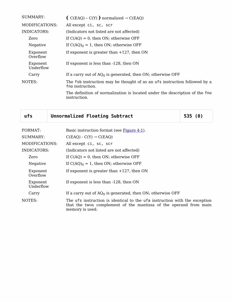
SUMMARY: ( C(EAQ) – C(Y) ) normalized C(EAQ)→
MODIFICATIONS: All except ci, sc, scr
INDICATORS: (Indicators not listed are not affected)
Zero If C(AQ) = 0, then ON; otherwise OFF
Negative If C(AQ)0 = 1, then ON; otherwise OFF
Exponent Overflow
If exponent is greater than +127, then ON
Exponent Underflow
If exponent is less than -128, then ON
Carry If a carry out of AQ0 is generated, then ON; otherwise OFF
NOTES: The fsb instruction may be thought of as an ufs instruction followed by a fno instruction.
The definition of normalization is located under the description of the fno instruction.
ufs Unnormalized Floating Subtract 535 (0)
FORMAT: Basic instruction format (see Figure 4-1).
SUMMARY: C(EAQ) - C(Y) C(EAQ)→
MODIFICATIONS: All except ci, sc, scr
INDICATORS: (Indicators not listed are not affected)
Zero If C(AQ) = 0, then ON; otherwise OFF
Negative If C(AQ)0 = 1, then ON; otherwise OFF
Exponent Overflow
If exponent is greater than +127, then ON
Exponent Underflow
If exponent is less than -128, then ON
Carry If a carry out of AQ0 is generated, then ON; otherwise OFF
NOTES: The ufs instruction is identical to the ufa instruction with the exception that the twos complement of the mantissa of the operand from main memory is used.

Floating-Point Multiplication
dfmp Double-Precision Floating Multiply 463 (0)
FORMAT: Basic instruction format (see Figure 4-1).
SUMMARY: ( C(EAQ) × C(Y-Pair) ) normalized C(EAQ)→
MODIFICATIONS: All except du, dl, ci, sc, scr
INDICATORS: (Indicators not listed are not affected)
Zero If C(AQ) = 0, then ON; otherwise OFF
Negative If C(AQ)0 = 1, then ON; otherwise OFF
Exponent Overflow
If exponent is greater than +127, then ON
Exponent Underflow
If exponent is less than -128, then ON
NOTES: The dfmp instruction may be thought of as a dufm instruction followed by a fno instruction.
The definition of normalization is located under the description of the fno instruction.
dufm Double-Precision Unnormalized Floating Multiply
423 (0)
FORMAT: Basic instruction format (see Figure 4-1).
SUMMARY: C(EAQ) × C(Y-pair) C(EAQ)→
MODIFICATIONS: All except du, dl, ci, sc, scr
INDICATORS: (Indicators not listed are not affected)
Zero If C(AQ) = 0, then ON; otherwise OFF
Negative If C(AQ)0 = 1, then ON; otherwise OFF
Exponent Overflow
If exponent is greater than +127, then ON
Exponent Underflow
If exponent is less than -128, then ON
NOTES: Except for the precision of the mantissa of the operand from main memory, the dufm instruction is identical to the ufm instruction.
fmp Floating Multiply 461 (0)
FORMAT: Basic instruction format (see Figure 4-1).
SUMMARY: ( C(EAQ) × C(Y) ) normalized C(EAQ)→

MODIFICATIONS: All except ci, sc, scr
INDICATORS: (Indicators not listed are not affected)
Zero If C(AQ) = 0, then ON; otherwise OFF
Negative If C(AQ)0 = 1, then ON; otherwise OFF
Exponent Overflow
If exponent is greater than +127, then ON
Exponent Underflow
If exponent is less than -128, then ON
NOTES: The fmp instruction may be thought of as a ufm instruction followed by a fno instruction.
The definition of normalization is located under the description of the fno instruction.
ufm Unnormalized Floating Multiply 421 (0)
FORMAT: Basic instruction format (see Figure 4-1).
SUMMARY: C(EAQ) × C(Y) C(EAQ)→
MODIFICATIONS: All except ci, sc, scr
INDICATORS: (Indicators not listed are not affected)
Zero If C(AQ) = 0, then ON; otherwise OFF
Negative If C(AQ)0 = 1, then ON; otherwise OFF
Exponent Overflow
If exponent is greater than +127, then ON
Exponent Underflow
If exponent is less than -128, then ON
NOTES: The ufm instruction is executed as follows:
C(E) + C(Y)0,7 C(E)→
( C(AQ) × C(Y)8,35 )0,71 C(AQ)→
A normalization is performed only in the case of both factor mantissas being 100...0 which is the twos complement approximation to the decimal value -1.0.
The definition of normalization is located under the description of the fno instruction.
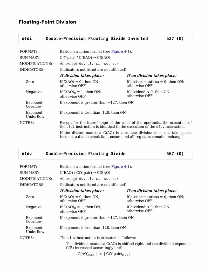
Floating-Point Division
dfdi Double-Precision Floating Divide Inverted 527 (0)
FORMAT: Basic instruction format (see Figure 4-1).
SUMMARY: C(Y-pair) / C(EAQ) C(EAQ)→
MODIFICATIONS: All except du, dl, ci, sc, scr
INDICATORS: (Indicators not listed are not affected)
If division takes place: If no division takes place:
Zero If C(AQ) = 0, then ON;otherwise OFF
If divisor mantissa = 0, then ON;otherwise OFF
Negative If C(AQ)0 = 1, then ON;otherwise OFF
If dividend < 0, then ON;otherwise OFF
Exponent Overflow
If exponent is greater than +127, then ON
Exponent Underflow
If exponent is less than -128, then ON
NOTES: Except for the interchange of the roles of the operands, the execution of the dfdi instruction is identical to the execution of the dfdv instruction.
If the divisor mantissa C(AQ) is zero, the division does not take place. Instead, a divide check fault occurs and all registers remain unchanged.
dfdv Double-Precision Floating Divide 567 (0)
FORMAT: Basic instruction format (see Figure 4-1).
SUMMARY: C(EAQ) / C(Y-pair) C(EAQ)→
MODIFICATIONS: All except du, dl, ci, sc, scr
INDICATORS: (Indicators not listed are not affected)
If division takes place: If no division takes place:
Zero If C(AQ) = 0, then ON;otherwise OFF
If divisor mantissa = 0, then ON;otherwise OFF
Negative If C(AQ)0 = 1, then ON;otherwise OFF
If dividend < 0, then ON;otherwise OFF
Exponent Overflow
If exponent is greater than +127, then ON
Exponent Underflow
If exponent is less than -128, then ON
NOTES: The dfdv instruction is executed as follows:
The dividend mantissa C(AQ) is shifted right and the dividend exponent C(E) increased accordingly until
| C(AQ)0,63 | < | C(Y-pair)8,71 |
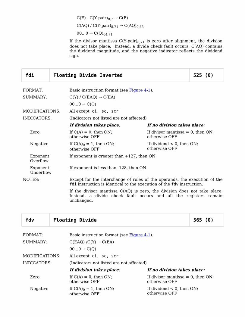
C(E) - C(Y-pair)0,7 C(E)→
C(AQ) / C(Y-pair)8,71 C(AQ)→ 0,63
00...0 C(Q)→ 64,71
If the divisor mantissa C(Y-pair)8,71 is zero after alignment, the division does not take place. Instead, a divide check fault occurs, C(AQ) contains the dividend magnitude, and the negative indicator reflects the dividend sign.
fdi Floating Divide Inverted 525 (0)
FORMAT: Basic instruction format (see Figure 4-1).
SUMMARY: C(Y) / C(EAQ) C(EA)→
00...0 C(Q)→
MODIFICATIONS: All except ci, sc, scr
INDICATORS: (Indicators not listed are not affected)
If division takes place: If no division takes place:
Zero If C(A) = 0, then ON;otherwise OFF
If divisor mantissa = 0, then ON;otherwise OFF
Negative If C(A)0 = 1, then ON;otherwise OFF
If dividend < 0, then ON;otherwise OFF
Exponent Overflow
If exponent is greater than +127, then ON
Exponent Underflow
If exponent is less than -128, then ON
NOTES: Except for the interchange of roles of the operands, the execution of the fdi instruction is identical to the execution of the fdv instruction.
If the divisor mantissa C(AQ) is zero, the division does not take place. Instead, a divide check fault occurs and all the registers remain unchanged.
fdv Floating Divide 565 (0)
FORMAT: Basic instruction format (see Figure 4-1).
SUMMARY: C(EAQ) /C(Y) C(EA)→
00...0 C(Q)→
MODIFICATIONS: All except ci, sc, scr
INDICATORS: (Indicators not listed are not affected)
If division takes place: If no division takes place:
Zero If C(A) = 0, then ON;otherwise OFF
If divisor mantissa = 0, then ON;otherwise OFF
Negative If C(A)0 = 1, then ON;otherwise OFF
If dividend < 0, then ON;otherwise OFF
Exponent Overflow
If exponent is greater than +127, then ON
Exponent Underflow
If exponent is less than -128, then ON
NOTES: The fdv instruction is executed as follows:
The dividend mantissa C(AQ) is shifted right and the dividend exponent C(E) increased accordingly until
| C(AQ)0,27 | < | C(Y)8,35 |
C(E) - C(Y)0,7 C(E)→
C(AQ) / C(Y)8,35 C(A)→
00...0 C(Q)→
If the divisor mantissa C(Y)8,35 is zero after alignment, the division does not take place. Instead, a divide check fault occurs, C(AQ) contains the dividend magnitude, and the negative indicator reflects the dividend sign.
Floating-Point Negate
fneg Floating Negate 513 (0)
FORMAT: Basic instruction format (see Figure 4-1).
SUMMARY: -C(EAQ) normalized C(EAQ)→
MODIFICATIONS: All, but none affect instruction execution.
INDICATORS: (Indicators not listed are not affected)
Zero If C(AQ) = 0, then ON; otherwise OFF
Negative If C(AQ)0 = 1, then ON; otherwise OFF
Exponent Overflow
If exponent is greater than +127, then ON
Exponent Underflow
If exponent is less than -128, then ON
NOTES: This instruction changes the number in C(EAQ) to its normalized negative (if C(AQ) ≠ 0). The operation is executed by first forming the twos complement of C(AQ), and then normalizing C(EAQ).
Even if originally C(EAQ) were normalized, an exponent overflow can still occur, namely when C(E) = +127 and C(AQ) = 100...0 which is the twos complement approximation for the decimal value -1.0.
The definition of normalization may be found under the description of the fno instruction.
Attempted repetition with the rpl instruction causes an illegal procedure fault.
Floating-Point Normalize
fno Floating Normalize 573 (0)
FORMAT: Basic instruction format (see Figure 4-1).
SUMMARY: C(EAQ) normalized C(EAQ)→
MODIFICATIONS: All, but none affect instruction execution.
INDICATORS: (Indicators not listed are not affected)
Zero If C(EAQ) = floating point 0, then ON; otherwise OFF
Negative If C(AQ)0 = 1, then ON; otherwise OFF
Exponent Overflow
If exponent is greater than +127, then ON
Exponent Underflow
If exponent is less than -128, then ON
Overflow Set OFF
NOTES: The fno instruction normalizes the number in C(EAQ) if C(AQ) ≠ 0 and the overflow indicator is OFF.
A normalized floating number is defined as one whose mantissa lies in the interval [0.5,1.0] such that
0.5 <= | C(AQ) | < 1.0
which, in turn, requires that C(AQ)0 ≠ C(AQ)1.
If the overflow indicator is ON, then C(AQ) is shifted one place to the right, C(AQ)0 is inverted to reconstitute the actual sign, and the overflow indicator is set OFF. This action makes the fno instruction useful in correcting overflows that occur with fixed point numbers.
Normalization is performed by shifting C(AQ)1,71 one place to the left and reducing C(E) by 1, repeatedly, until the conditions for C(AQ)0 and C(AQ)1 are met. Bits shifted out of AQ1 are lost.
If C(AQ) = 0, then C(E) is set to -128 and the zero indicator is set ON.
Attempted repetition with the rpl instruction causes an illegal procedure fault.
Floating-Point Round
dfrd Double-Precision Floating Round 473 (0)
FORMAT: Basic instruction format (see Figure 4-1).
SUMMARY: C(EAQ) rounded to 64 bits C(EAQ)→
0 C(AQ)→ 65,71
MODIFICATIONS: All, but none affect instruction execution.
INDICATORS: (Indicators not listed are not affected)
Zero If C(EAQ) = floating point 0, then ON; otherwise OFF
Negative If C(AQ)0 = 1, then ON; otherwise OFF
Exponent Overflow
If exponent is greater than +127, then ON
Exponent Underflow
If exponent is less than -128, then ON
NOTES: The dfrd instruction is identical to the frd instruction except that the rounding constant used is (11...1)65,71 instead of (11...1)29,71.
Attempted repetition with the rpl instruction causes an illegal procedure fault
frd Floating Round 471 (0)
FORMAT: Basic instruction format (see Figure 4-1).
SUMMARY: C(EAQ) rounded to 28 bits C(EAQ)→
0 C(AQ)→ 29,71
MODIFICATIONS: All, but none affect instruction execution.
INDICATORS: (Indicators not listed are not affected)
Zero If C(EAQ) = floating point 0, then ON; otherwise OFF
Negative If C(AQ)0 = 1 then ON; otherwise OFF
Exponent Overflow
If exponent is greater than +127, then ON
Exponent Underflow
If exponent is less than -128, then ON
NOTES: If C(AQ) ≠ 0, the frd instruction performs a true round to a precision of 28 bits and a normalization on C(EAQ).
A true round is a rounding operation such that the sum of the result of applying the operation to two numbers of equal magnitude but opposite sign is exactly zero.

The frd instruction is executed as follows:
C(AQ) + (11...1)29,71 C(AQ)→
If C(AQ)0 = 0, then a carry is added at AQ71
If overflow occurs, C(AQ) is shifted one place to the right and C(E) is increased by 1.
If overflow does not occur, C(EAQ) is normalized.
If C(AQ) = 0, C(E) is set to -128 and the zero indicator is set ON.
Attempted repetition with the rpl instruction causes an illegal procedure fault.
Floating-Point Compare
dfcmg Double-Precision Floating Compare Magnitude 427 (0)
FORMAT: Basic instruction format (see Figure 4-1).
SUMMARY: C(E) :: C(Y-pair)0,7
| C(AQ)0,63 | :: | C(Y-pair)8,71 |
MODIFICATIONS: All except du, dl, ci, sc, scr
INDICATORS: (Indicators not listed are not affected)
Zero If | C(EAQ) | = | C(Y-pair) | , then ON; otherwise OFF
Negative If | C(EAQ) | < | C(Y-pair) | , then ON; otherwise OFF
NOTES: The dfcmg instruction is identical to the dfcmp instruction except that the magnitudes of the mantissas are compared instead of the algebraic values.
dfcmp Double-Precision Floating Compare 517 (0)
FORMAT: Basic instruction format (see Figure 4-1).
SUMMARY: C(E) :: C(Y-pair)0,7
C(AQ)0,63 :: C(Y-pair)8,71
MODIFICATIONS: All except du, dl, ci, sc, scr
INDICATORS: (Indicators not listed are not affected)
Zero If C(EAQ) = C(Y-pair), then ON; otherwise OFF
Negative If C(EAQ) < C(Y-pair), then ON; otherwise OFF
NOTES: The dfcmp instruction is identical to the fcmp instruction except for the precision of the mantissas actually compared.
fcmg Floating Compare Magnitude 425 (0)
FORMAT: Basic instruction format (see Figure 4-1).
SUMMARY: C(E) :: C(Y)0,7
| C(AQ)0,27 | :: | C(Y)8,35 |
MODIFICATIONS: All except ci, sc, scr
INDICATORS: (Indicators not listed are not affected)
Zero If | C(EAQ) | = | C(Y) | , then ON; otherwise OFF
Negative If | C(EAQ) | < | C(Y) | , then ON; otherwise OFF
NOTES: The fcmg instruction is identical to the fcmp instruction except that the magnitudes of the mantissas are compared instead of the algebraic values.

fcmp Floating Compare 515 (0)
FORMAT: Basic instruction format (see Figure 4-1).
SUMMARY: C(E) :: C(Y)0,7
C(AQ)0,27 :: C(Y)8,35
MODIFICATIONS: All except ci, sc, scr
INDICATORS: (Indicators not listed are not affected)
Zero If C(EAQ) = C(Y), then ON; otherwise OFF
Negative If C(EAQ) < C(Y), then ON; otherwise OFF
NOTES: The fcmp instruction is executed as follows:
The mantissas are aligned by shifting the mantissa of the operand with the algebraically smaller exponent to the right the number of places equal to the difference in the two exponents.
The aligned mantissas are compared and the indicators set accordingly.
Floating-Point Miscellaneous
ade Add to Exponent 415 (0)
FORMAT: Basic instruction format (see Figure 4-1).
SUMMARY: C(E) + C(Y)0,7 C(E)→
MODIFICATIONS: All except ci, sc, scr
INDICATORS: (Indicators not listed are not affected)
Zero Set OFF
Negative Set OFF
Exponent Overflow
If exponent is greater than +127, then ON
Exponent Underflow
If exponent is less than -128, then ON
fszn Floating Set Zero and Negative Indicators 430 (0)
FORMAT: Basic instruction format (see Figure 4-1).
SUMMARY: Set indicators according to C(Y)
MODIFICATIONS: All except ci, sc, scr
INDICATORS: (Indicators not listed are not affected)
Zero If C(Y)8,35 = 0, then ON; otherwise OFF
Negative If C(Y)8 = 1, then ON; otherwise OFF
lde Load Exponent 411 (0)
FORMAT: Basic instruction format (see Figure 4-1).
SUMMARY: C(Y)0,7 C(E)→
MODIFICATIONS: All except ci, sc, scr
INDICATORS: (Indicators not listed are not affected)
Zero Set OFF
Negative Set OFF
ste Store Exponent 456 (0)
FORMAT: Basic instruction format (see Figure 4-1).

SUMMARY: C(E) C(Y)→ 0,7
00...0 C(Y)→ 8,17
MODIFICATIONS: All except du, dl, ci, sc, scr
INDICATORS: None affected
TRANSFER INSTRUCTIONS
call6 Call (Using PR6 and PR7) 713 (0)
FORMAT: Basic instruction format (see Figure 4-1).
SUMMARY: If C(TPR.TRR) < C(PPR.PRR) then
C(DSBR.STACK) || C(TPR.TRR) C(PR7.SNR)→
If C(TPR.TRR) = C(PPR.PRR) then C(PR6.SNR) C(PR7.SNR)→
C(TPR.TRR) C(PR7.RNR)→
If C(TPR.TRR) = 0 then C(SDW.P) C(PPR.P);→
otherwise 0 C(PPR.P)→
00...0 C(PR7.WORDNO)→
00...0 C(PR7.BITNO)→
C(TPR.TRR) C(PPR.PRR)→
C(TPR.TSR) C(PPR.PSR)→
C(TPR.CA) C(PPR.IC)→
MODIFICATIONS: All except du, dl, ci, sc, scr
INDICATORS: None affected
NOTES: See Section 3 for descriptions of the various registers and Section 8 for a flowchart of their role in address preparation.
If C(TPR.TRR) > C(PPR.PRR), an access violation fault (outward call) occurs and the call6 instruction is not executed.
If the call6 instruction is executed with the processor in absolute mode with bit 29 of the instruction word set OFF and without indirection through an ITP or ITS pair, then:
the appending mode is entered for the address preparation of the call6 operand address and is retained if the instruction executes successfully,
and the effective segment number generated for the SDW fetch and subsequent loading into C(TPR.TSR) is equal to C(PPR.PSR) and may be undefined in absolute mode,
and the effective ring number loaded into C(TPR.TRR) prior to the SDW fetch is equal to C(PPR.PRR) (which is 0 in absolute mode) implying that the access violation checks for outward call and bad outward call are ineffective and that an access violation (out of call brackets) will occur if C(SDW.R1) ≠ 0.
Attempted repetition with the rpt, rpd, or rpl instructions causes an illegal procedure fault.
ret Return 630 (0)
FORMAT: Basic instruction format (see Figure 4-1).

SUMMARY: C(Y)0,17 C(PPR.IC)→
C(Y)18,31 C(IR)→
MODIFICATIONS: All except du, dl, ci, sc, scr
INDICATORS: (Indicators not listed are not affected)
Parity mask If C(Y)27 = 1, and the processor is in absolute or mask privileged mode, then ON; otherwise OFF. This indicator is not affected in the normal or BAR modes.
Not BAR mode Can be set OFF but not ON by the ret instruction
Absolute mode Can be set OFF but not ON by the ret instruction
All other indicators
If corresponding bit in C(Y) is 1, then ON; otherwise, OFF
NOTES: The relation between C(Y)18,31 and the indicators is given in Table 4-5 earlier in this section.
The tally runout indicator reflects C(Y)25 regardless of what address modification is performed on the ret instruction.
The ret instruction may be thought of as a ldi instruction followed by a transfer to location C(Y)0,17.
Attempted repetition with the rpt, rpd, or rpl instructions causes an illegal procedure fault.
rtcd Return Control Double 610 (0)
FORMAT: Basic instruction format (see Figure 4-1).
SUMMARY: C(Y-pair)3,17 C(PPR.PSR)→
Maximum of
C(Y-pair)18,20; C(TPR.TRR); C(SDW.R1) C(PPR.PRR)→
C(Y-pair)36,53 C(PPR.IC)→
If C(PPR.PRR) = 0 then C(SDW.P) C(PPR.P);→
otherwise 0 C(PPR.P)→
C(PPR.PRR) C(PRn.RNR) for n = (0, 1, ..., 7)→
MODIFICATIONS: All except du, dl, ci, sc, scr
INDICATORS: None affected
NOTES: See Section 3 for descriptions of the various registers and Section 8 for a flowchart of their role in address preparation.
If an access violation fault occurs when fetching the SDW for the Y-pair, the C(PPR.PSR) and C(PPR.PRR) are not altered.
If the rtcd instruction is executed with the processor in absolute mode with bit 29 of the instruction word set OFF and without indirection through an ITP or ITS pair, then:
appending mode is entered for address preparation for the rtcd operand and is retained if the instruction executes successfully,
and the effective segment number generated for the SDW fetch and subsequent loading into C(TPR.TSR) is equal to C(PPR.PSR) and may be undefined in absolute mode,

and the effective ring number loaded into C(TPR.TRR) prior to the SDW fetch is equal to C(PPR.PRR) (which is 0 in absolute mode) implying that control is always transferred into ring 0.
Attempted repetition with the rpt, rpd, or rpl instructions causes an illegal procedure fault.
teo Transfer on Exponent Overflow 614 (0)
FORMAT: Basic instruction format (see Figure 4-1).
SUMMARY: If exponent overflow indicator ON then
C(TPR.CA) C(PPR.IC)→
C(TPR.TSR) C(PPR.PSR)→
otherwise, no change to C(PPR)
MODIFICATIONS: All except du, dl, ci, sc, scr
INDICATORS: (Indicators not listed are not affected)
Exponent overflow
Set OFF
NOTES: Attempted repetition with the rpt, rpd, or rpl instructions causes an illegal procedure fault.
teu Transfer on Exponent Underflow 615 (0)
FORMAT: Basic instruction format (see Figure 4-1).
SUMMARY: If exponent underflow indicator ON then
C(TPR.CA) C(PPR.IC)→
C(TPR.TSR) C(PPR.PSR)→
otherwise, no change to C(PPR)
MODIFICATIONS: All except du, dl, ci, sc, scr
INDICATORS: (Indicators not listed are not affected)
Exponent underflow
Set OFF
NOTES: Attempted repetition with the rpt, rpd, or rpl instructions causes an illegal procedure fault.
tmi Transfer on Minus 604 (0)
FORMAT: Basic instruction format (see Figure 4-1).
SUMMARY: If negative indicator ON then
C(TPR.CA) C(PPR.IC)→
C(TPR.TSR) C(PPR.PSR)→
otherwise, no change to C(PPR)
MODIFICATIONS: All except du, dl, ci, sc, scr
INDICATORS: None affected
NOTES: Attempted repetition with the rpt, rpd, or rpl instructions causes an illegal procedure fault.
tmoz Transfer on Minus or Zero 604 (1)
FORMAT: Basic instruction format (see Figure 4-1).
SUMMARY: If negative or zero indicator ON then
C(TPR.CA) C(PPR.IC)→
C(TPR.TSR) C(PPR.PSR)→
otherwise, no change to C(PPR)
MODIFICATIONS: All except du, dl, ci, sc, scr
INDICATORS: None affected
NOTES: Attempted repetition with the rpt, rpd, or rpl instructions causes an illegal procedure fault.
tnc Transfer on No Carry 602 (0)
FORMAT: Basic instruction format (see Figure 4-1).
SUMMARY: If carry indicator OFF then
C(TPR.CA) C(PPR.IC)→
C(TPR.TSR) C(PPR.PSR)→
otherwise, no change to C(PPR)
MODIFICATIONS: All except du, dl, ci, sc, scr
INDICATORS: None affected
NOTES: Attempted repetition with the rpt, rpd, or rpl instructions causes an illegal procedure fault.
tnz Transfer on Nonzero 601 (0)
FORMAT: Basic instruction format (see Figure 4-1).
SUMMARY: If zero indicator OFF then
C(TPR.CA) C(PPR.IC)→
C(TPR.TSR) C(PPR.PSR)→
otherwise, no change to C(PPR)
MODIFICATIONS: All except du, dl, ci, sc, scr
INDICATORS: None affected
NOTES: Attempted repetition with the rpt, rpd, or rpl instructions causes an illegal procedure fault.
tov Transfer on Overflow 617 (0)
FORMAT: Basic instruction format (see Figure 4-1).
SUMMARY: If overflow indicator ON then
C(TPR.CA) C(PPR.IC)→
C(TPR.TSR) C(PPR.PSR)→
otherwise, no change to C(PPR)
MODIFICATIONS: All except du, dl, ci, sc, scr
INDICATORS: (Indicators not listed are not affected)
Overflow Set OFF
NOTES: Attempted repetition with the rpt, rpd, or rpl instructions causes an illegal procedure fault.
tpl Transfer on Plus 605 (0)
FORMAT: Basic instruction format (see Figure 4-1).
SUMMARY: If negative indicator OFF, then
C(TPR.CA) C(PPR.IC)→
C(TPR.TSR) C(PPR.PSR)→
otherwise, no change to C(PPR)
MODIFICATIONS: All except du, dl, ci, sc, scr
INDICATORS: None affected
NOTES: Attempted repetition with the rpt, rpd, or rpl instructions causes an illegal procedure fault.
tpnz Transfer on Plus and Nonzero 605 (1)
FORMAT: Basic instruction format (see Figure 4-1).
SUMMARY: If negative and zero indicators are OFF then
C(TPR.CA) C(PPR.IC)→
C(TPR.TSR) C(PPR.PSR)→
otherwise, no change to C(PPR)
MODIFICATIONS: All except du, dl, ci, sc, scr
INDICATORS: None affected
NOTES: Attempted repetition with the rpt, rpd, or rpl instructions causes an illegal procedure fault.
tra Transfer Unconditionally 710 (0)
FORMAT: Basic instruction format (see Figure 4-1).
SUMMARY: C(TPR.CA) C(PPR.IC)→
C(TPR.TSR) C(PPR.PSR)→
MODIFICATIONS: All except du, dl, ci, sc, scr
INDICATORS: None affected
NOTES: Attempted repetition with the rpt, rpd, or rpl instructions causes an illegal procedure fault.
trc Transfer on Carry 603 (0)
FORMAT: Basic instruction format (see Figure 4-1).
SUMMARY: If carry indicator ON then
C(TPR.CA) C(PPR.IC)→
C(TPR.TSR) C(PPR.PSR)→
otherwise, no change to C(PPR)
MODIFICATIONS: All except du, dl, ci, sc, scr
INDICATORS: None affected
NOTES: Attempted repetition with the rpt, rpd, or rpl instructions causes an illegal procedure fault.
trtf Transfer on Truncation Indicator OFF 601 (1)
FORMAT: Basic instruction format (see Figure 4-1).
SUMMARY: If truncation indicator OFF then
C(TPR.CA) C(PPR.IC)→
C(TPR.TSR) C(PPR.PSR)→
otherwise, no change to C(PPR)
MODIFICATIONS: All except du, dl, ci, sc, scr

INDICATORS: None affected
NOTES: Attempted repetition with the rpt, rpd, or rpl instructions causes an illegal procedure fault.
trtn Transfer on Truncation Indicator ON 600 (1)
FORMAT: Basic instruction format (see Figure 4-1).
SUMMARY: If truncation indicator ON then
C(TPR.CA) C(PPR.IC)→
C(TPR.TSR) C(PPR.PSR)→
otherwise, no change to C(PPR)
MODIFICATIONS: All except du, dl, ci, sc, scr
INDICATORS: (Indicators not listed are not affected)
Truncation Set OFF
NOTES: Attempted repetition with the rpt, rpd, or rpl instructions causes an illegal procedure fault.
tsp0 Transfer and Set Pointer Register 0 270 (0)
tsp1 Transfer and Set Pointer Register 1 271 (0)
tsp2 Transfer and Set Pointer Register 2 272 (0)
tsp3 Transfer and Set Pointer Register 3 273 (0)
tsp4 Transfer and Set Pointer Register 4 670 (0)
tsp5 Transfer and Set Pointer Register 5 671 (0)
tsp6 Transfer and Set Pointer Register 6 672 (0)
tsp7 Transfer and Set Pointer Register 7 673 (0)
FORMAT: Basic instruction format (see Figure 4-1).
SUMMARY: For n = 0, 1, ..., or 7 as determined by operation code
C(PPR.PRR) C(PRn.RNR)→
C(PPR.PSR) C(PRn.SNR)→
C(PPR.IC) + 1 C(PRn.WORDNO)→
00...0 C(PRn.BITNO)→
C(TPR.CA) C(PPR.IC)→
C(TPR.TSR) C(PPR.PSR)→
MODIFICATIONS: All except du, dl, ci, sc, scr
INDICATORS: None affected
NOTES: Attempted repetition with the rpt, rpd, or rpl instructions causes an illegal procedure fault.
tss Transfer and Set Slave 715 (0)
FORMAT: Basic instruction format (see Figure 4-1).
SUMMARY: C(TPR.CA) + (BAR base) C(PPR.IC)→
C(TPR.TSR) C(PPR.PSR)→
MODIFICATIONS: All except du, dl, ci, sc, scr
INDICATORS: (Indicators not listed are not affected)
Not BAR mode Set OFF (see notes below)
Absolute mode Set OFF
NOTES: If the tss instruction is executed with the processor not in BAR mode the not BAR mode indicator is set OFF to enable subsequent addressing in the BAR mode. The base address register (BAR) is used in the address preparation of the transfer, and the BAR will be used in address preparation for all subsequent instructions until a fault or interrupt occurs.
If the tss instruction is executed with the not BAR mode indicator already OFF, it functions as a tra instruction and no indicators are changed.
If C(TPR.CA) >= (BAR bound) the transfer does not take place. Instead, a store fault (out of bounds) occurs.
Attempted repetition with the rpt, rpd, or rpl instructions causes an illegal procedure fault.
tsxn Transfer and Set Index Register n 70n (0)
FORMAT: Basic instruction format (see Figure 4-1).
SUMMARY: For n = 0, 1, ..., or 7 as determined by operation code
C(PPR.IC) + 1 C(Xn)→
C(TPR.CA) C(PPR.IC)→
C(TPR.TSR) C(PPR.PSR)→
MODIFICATIONS: All except du, dl, ci, sc, scr
INDICATORS: None affected
NOTES: Attempted repetition with the rpt, rpd, or rpl instructions causes an illegal procedure fault.
ttf Transfer on Tally Runout Indicator OFF 607 (0)
FORMAT: Basic instruction format (see Figure 4-1).
SUMMARY: If tally runout indicator OFF then
C(TPR.CA) C(PPR.IC)→
C(TPR.TSR) C(PPR.PSR)→
otherwise, no change to C(PPR)
MODIFICATIONS: All except du, dl, ci, sc, scr
INDICATORS: None affected
NOTES: Attempted repetition with the rpt, rpd, or rpl instructions causes an illegal procedure fault.
ttn Transfer on Tally Runout Indicator ON 606 (1)
FORMAT: Basic instruction format (see Figure 4-1).
SUMMARY: If tally runout indicator ON then
C(TPR.CA) C(PPR.IC)→
C(TPR.TSR) C(PPR.PSR)→
otherwise, no change to C(PPR)
MODIFICATIONS: All except du, dl, ci, sc, scr
INDICATORS: None affected
NOTES: Attempted repetition with the rpt, rpd, or rpl instructions causes an illegal procedure fault.
tze Transfer on Zero 600 (0)
FORMAT: Basic instruction format (see Figure 4-1).
SUMMARY: If zero indicator ON then
C(TPR.CA) C(PPR.IC)→
C(TPR.TSR) C(PPR.PSR)→
otherwise, no change to C(PPR)
MODIFICATIONS: All except du, dl, ci, sc, scr
INDICATORS: None affected
NOTES: Attempted repetition with the rpt, rpd, or rpl instructions causes an illegal procedure fault.

POINTER REGISTER INSTRUCTIONS
Pointer Register Data Movement Load
easp0 Effective Address to Segment Number of PR0 311 (0)
easp1 Effective Address to Segment Number of PR1 310 (1)
easp2 Effective Address to Segment Number of PR2 313 (0)
easp3 Effective Address to Segment Number of PR3 312 (1)
easp4 Effective Address to Segment Number of PR4 331 (0)
easp5 Effective Address to Segment Number of PR5 330 (1)
easp6 Effective Address to Segment Number of PR6 333 (0)
easp7 Effective Address to Segment Number of PR7 332 (1)
FORMAT: Basic instruction format (see Figure 4-1).
SUMMARY: For n = 0, 1, ..., or 7 as determined by operation code
C(TPR.CA) C(PRn.SNR)→
MODIFICATIONS: All except du, dl, ci, sc, scr
INDICATORS: None affected
NOTES: Attempted execution in BAR mode causes an illegal procedure fault.
Attempted repetition with the rpt, rpd, or rpl instructions causes an illegal procedure fault.
eawp0 Effective Address to Word/Bit Number of PR0 310 (0)
eawp1 Effective Address to Word/Bit Number of PR1 311 (1)
eawp2 Effective Address to Word/Bit Number of PR2 312 (0)
eawp3 Effective Address to Word/Bit Number of PR3 313 (1)
eawp4 Effective to Word/Bit Number of PR4 Address 330 (0)
eawp5 Effective Address to Word/Bit Number of PR5 331 (1)
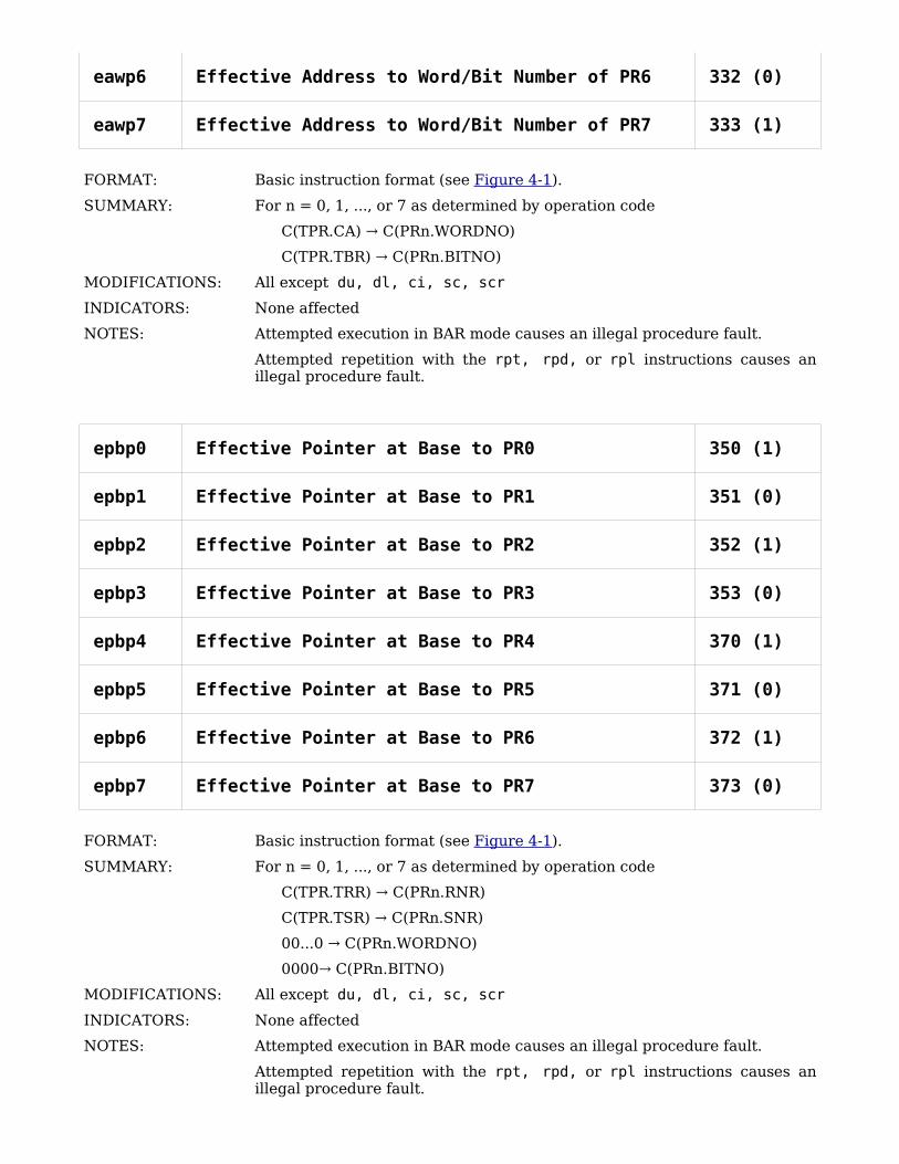
eawp6 Effective Address to Word/Bit Number of PR6 332 (0)
eawp7 Effective Address to Word/Bit Number of PR7 333 (1)
FORMAT: Basic instruction format (see Figure 4-1).
SUMMARY: For n = 0, 1, ..., or 7 as determined by operation code
C(TPR.CA) C(PRn.WORDNO)→
C(TPR.TBR) C(PRn.BITNO)→
MODIFICATIONS: All except du, dl, ci, sc, scr
INDICATORS: None affected
NOTES: Attempted execution in BAR mode causes an illegal procedure fault.
Attempted repetition with the rpt, rpd, or rpl instructions causes an illegal procedure fault.
epbp0 Effective Pointer at Base to PR0 350 (1)
epbp1 Effective Pointer at Base to PR1 351 (0)
epbp2 Effective Pointer at Base to PR2 352 (1)
epbp3 Effective Pointer at Base to PR3 353 (0)
epbp4 Effective Pointer at Base to PR4 370 (1)
epbp5 Effective Pointer at Base to PR5 371 (0)
epbp6 Effective Pointer at Base to PR6 372 (1)
epbp7 Effective Pointer at Base to PR7 373 (0)
FORMAT: Basic instruction format (see Figure 4-1).
SUMMARY: For n = 0, 1, ..., or 7 as determined by operation code
C(TPR.TRR) C(PRn.RNR)→
C(TPR.TSR) C(PRn.SNR)→
00...0 C(PRn.WORDNO)→
0000 C(PRn.BITNO)→
MODIFICATIONS: All except du, dl, ci, sc, scr
INDICATORS: None affected
NOTES: Attempted execution in BAR mode causes an illegal procedure fault.
Attempted repetition with the rpt, rpd, or rpl instructions causes an illegal procedure fault.

epp0 Effective Pointer to Pointer Register 0 350 (0)
epp1 Effective Pointer to Pointer Register 1 351 (1)
epp2 Effective Pointer to Pointer Register 2 352 (0)
epp3 Effective Pointer to Pointer Register 3 353 (1)
epp4 Effective Pointer to Pointer Register 4 370 (0)
epp5 Effective Pointer to Pointer Register 5 371 (1)
epp6 Effective Pointer to Pointer Register 6 372 (0)
epp7 Effective Pointer to Pointer Register 7 373 (1)
FORMAT: Basic instruction format (see Figure 4-1).
SUMMARY: For n = 0, 1, ..., or 7 as determined by operation code
C(TPR.TRR) C(PRn.RNR)→
C(TPR.TSR) C(PRn.SNR)→
C(TPR.CA) C(PRn.WORDNO)→
C(TPR.TBR) C(PRn.BITNO)→
MODIFICATIONS: All except du, dl, ci, sc, scr
INDICATORS: None affected
NOTES: Attempted execution in BAR mode causes an illegal procedure fault.
Attempted repetition with the rpt, rpd, or rpl instructions causes an illegal procedure fault.
lpri Load Pointer Registers from ITS Pairs 173 (0)
FORMAT: Basic instruction format (see Figure 4-1).
SUMMARY: For n = 0, 1, ..., 7
Y-pair = Y-block16 + 2n
Maximum of
C(Y-pair)18,20; C(SDW.R1); C(TPR.TRR) C(PRn.RNR)→
C(Y-pair)3,17 C(PRn.SNR)→
C(Y-pair)36,53 C(PRn.WORDNO)→
C(Y-pair)57,62 C(PRn.BITNO)→
MODIFICATIONS: All except du, dl, ci, sc, scr
INDICATORS: None affected

NOTES: Starting at location Y-block16, the contents of eight word pairs (in ITS pair format) replace the contents of pointer registers 0 through 7 as shown.
Since C(TPR.TRR) and C(SDW.R1) are both equal to zero in absolute mode, C(Y-pair)18,20 are loaded into PRn.RNR in absolute mode.
Attempted execution in BAR mode causes an illegal procedure fault.
Attempted repetition with the rpt, rpd, or rpl instructions causes an illegal procedure fault.
lprpn Load Pointer Register n Packed 76n (0)
FORMAT: Basic instruction format (see Figure 4-1).
SUMMARY: For n = 0, 1, ..., or 7 as determined by operation code
C(TPR.TRR) C(PRn.RNR)→
If C(Y)0,1 ≠ 11, then
C(Y)0,5 C(PRn.BITNO);→
otherwise, generate command fault
If C(Y)6,17 = ll...1, then 111 C(PRn.SNR)→ 0,2
otherwise, 000 C(PRn.SNR)→ 0,2
C(Y)6,17 C(PRn.SNR)→ 3,14
C(Y)18,35 C(PRn.WORDNO)→
MODIFICATIONS: All except du, dl, ci, sc, scr
INDICATORS: None affected
NOTES: Binary 1s in C(Y)0,1 correspond to an illegal BITNO, that is, a bit position beyond the extent of C(Y). Detection of these bits causes a command fault.
Attempted execution in BAR mode causes an illegal procedure fault.
Attempted repetition with the rpt, rpd, or rpl instructions causes an illegal procedure fault.

Pointer Register Data Movement Store
spbp0 Store Segment Base Pointer of PR0 250 (1)
spbp1 Store Segment Base Pointer of PR1 251 (0)
spbp2 Store Segment Base Pointer of PR2 252 (1)
spbp3 Store Segment Base Pointer of PR3 253 (0)
spbp4 Store Segment Base Pointer of PR4 650 (1)
spbp5 Store Segment Base Pointer of PR5 651 (0)
spbp6 Store Segment Base Pointer of PR6 652 (1)
spbp7 Store Segment Base Pointer of PR7 653 (0)
FORMAT: Basic instruction format (see Figure 4-1).
SUMMARY: For n = 0, 1, ..., or 7 as determined by operation code
C(PRn.SNR) C(Y-pair)→ 3,17
C(PRn.RNR) C(Y-pair)→ 18,20
000 C(Y-pair)→ 0,2
00...0 C(Y-pair)→ 21,29
(43)8 C(Y-pair)→ 30,35
00...0 C(Y-pair)→ 36,71
MODIFICATIONS: All except du, dl, ci, sc, scr
INDICATORS: None affected
NOTES: Attempted execution in BAR mode causes an illegal procedure fault.
Attempted repetition with the rpt, rpd, or rpl instructions causes an illegal procedure fault.
spri Store Pointer Registers as ITS Pairs 254 (0)
FORMAT: Basic instruction format (see Figure 4-1).
SUMMARY: For n = 0, 1, ..., 7
Y-pair = Y-block16 + 2n
000 C(Y-pair)→ 0,2
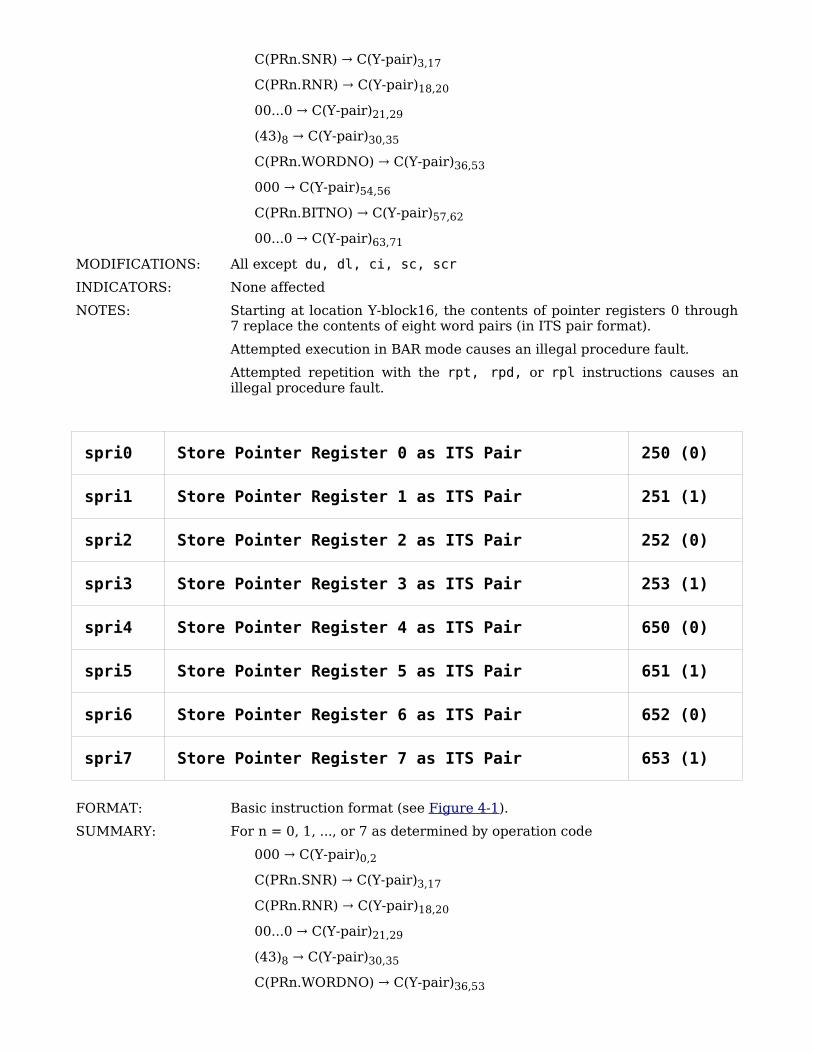
C(PRn.SNR) C(Y-pair)→ 3,17
C(PRn.RNR) C(Y-pair)→ 18,20
00...0 C(Y-pair)→ 21,29
(43)8 C(Y-pair)→ 30,35
C(PRn.WORDNO) C(Y-pair)→ 36,53
000 C(Y-pair)→ 54,56
C(PRn.BITNO) C(Y-pair)→ 57,62
00...0 C(Y-pair)→ 63,71
MODIFICATIONS: All except du, dl, ci, sc, scr
INDICATORS: None affected
NOTES: Starting at location Y-block16, the contents of pointer registers 0 through 7 replace the contents of eight word pairs (in ITS pair format).
Attempted execution in BAR mode causes an illegal procedure fault.
Attempted repetition with the rpt, rpd, or rpl instructions causes an illegal procedure fault.
spri0 Store Pointer Register 0 as ITS Pair 250 (0)
spri1 Store Pointer Register 1 as ITS Pair 251 (1)
spri2 Store Pointer Register 2 as ITS Pair 252 (0)
spri3 Store Pointer Register 3 as ITS Pair 253 (1)
spri4 Store Pointer Register 4 as ITS Pair 650 (0)
spri5 Store Pointer Register 5 as ITS Pair 651 (1)
spri6 Store Pointer Register 6 as ITS Pair 652 (0)
spri7 Store Pointer Register 7 as ITS Pair 653 (1)
FORMAT: Basic instruction format (see Figure 4-1).
SUMMARY: For n = 0, 1, ..., or 7 as determined by operation code
000 C(Y-pair)→ 0,2
C(PRn.SNR) C(Y-pair)→ 3,17
C(PRn.RNR) C(Y-pair)→ 18,20
00...0 C(Y-pair)→ 21,29
(43)8 C(Y-pair)→ 30,35
C(PRn.WORDNO) C(Y-pair)→ 36,53

000 C(Y-pair)→ 54,56
C(PRn.BITNO) C(Y-pair)→ 57,62
00...0 C(Y-pair)→ 63,71
MODIFICATIONS: All except du, dl, ci, sc, scr
INDICATORS: None affected
NOTES: Attempted execution in BAR mode causes an illegal procedure fault.
Attempted repetition with the rpt, rpd, or rpl instructions causes an illegal procedure fault.
sprpn Store Pointer Register n Packed 54n (0
FORMAT: Basic instruction format (see Figure 4-1).
SUMMARY: For n = 0, 1, ..., or 7 as determined by operation code
C(PRn.BITNO) C(Y)→ 0,5
C(PRn.SNR)3,14 C(Y)→ 6,17
C(PRn.WORDNO) C(Y)→ 18,35
MODIFICATIONS: All except du, dl, ci, sc, scr
INDICATORS: None affected
NOTES: If C(PRn.SNR)0,2 are nonzero, and C(PRn.SNR) ≠ 11...1, then a store fault (illegal pointer) will occur and C(Y) will not be changed.
Attempted execution in BAR mode causes an illegal procedure fault.
Attempted repetition with the rpt, rpd, or rpl instructions causes an illegal procedure fault.

Pointer Register Address Arithmetic
adwp0 Add to Word Number of Pointer Register 0 050 (0)
adwp1 Add to Word Number of Pointer Register 1 051 (0)
adwp2 Add to Word Number of Pointer Register 2 052 (0)
adwp3 Add to Word Number of Pointer Register 3 053 (0)
adwp4 Add to Word Number of Pointer Register 4 150 (0)
adwp5 Add to Word Number of Pointer Register 5 151 (0)
adwp6 Add to Word Number of Pointer Register 6 152 (0)
adwp7 Add to Word Number of Pointer Register 7 153 (0)
FORMAT: Basic instruction format (see Figure 4-1).
SUMMARY: For n = 0, 1, ..., or 7 as determined by operation code
C(Y)0,17 + C(PRn.WORDNO) C(PRn.WORDNO)→
00...0 C(PRn.BITNO)→
MODIFICATIONS: All except dl, ci, sc, scr
INDICATORS: None affected
NOTES: Attempted execution in BAR mode causes an illegal procedure fault.
Attempted repetition with the rpt, rpd, or rpl instructions causes an illegal procedure fault.
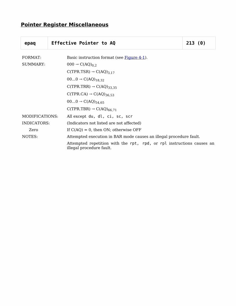
Pointer Register Miscellaneous
epaq Effective Pointer to AQ 213 (0)
FORMAT: Basic instruction format (see Figure 4-1).
SUMMARY: 000 C(AQ)→ 0,2
C(TPR.TSR) C(AQ)→ 3,17
00...0 C(AQ)→ 18,32
C(TPR.TRR) C(AQ)→ 33,35
C(TPR.CA) C(AQ)→ 36,53
00...0 C(AQ)→ 54,65
C(TPR.TBR) C(AQ)→ 66,71
MODIFICATIONS: All except du, dl, ci, sc, scr
INDICATORS: (Indicators not listed are not affected)
Zero If C(AQ) = 0, then ON; otherwise OFF
NOTES: Attempted execution in BAR mode causes an illegal procedure fault.
Attempted repetition with the rpt, rpd, or rpl instructions causes an illegal procedure fault.

MISCELLANEOUS INSTRUCTIONS
Calendar Clock
rccl Read Calendar Clock 633 (0)
FORMAT: Basic instruction format (see Figure 4-1).
SUMMARY: 00...0 C(AQ)→ 0,19
C(calendar clock) C(AQ)→ 20,71
MODIFICATIONS: All except du, dl, ci, sc, scr
INDICATORS: None affected
NOTES: C(TPR.CA)0,2 (C(TPR.CA)1,2 for the DPS 8M processor) specify which processor port (i.e., which system controller) is to be used. The contents of the clock in the designated system controller replace the contents of the AQ-register
Attempted execution in BAR mode causes an illegal procedure fault.
Attempted repetition with the rpt, rpd, or rpl instructions causes an illegal procedure fault.

Derail
drl Derail 002 (0)
FORMAT: Basic instruction format (see Figure 4-1).
SUMMARY: Causes a fault which fetches and executes, in absolute mode, the instruction pair at main memory location C+(14)8. The value of C is obtained from the FAULT VECTOR switches on the processor configuration panel.
MODIFICATIONS: All, but none affect instruction execution
INDICATORS: None affected
NOTES: Except for the different constant used for fetching the instruction pair from main memory, the drl instruction is identical to the mme instruction.
Attempted repetition with the rpt, rpd, or rpl instructions causes an illegal procedure fault.

Execute
xec Execute 716 (0)
FORMAT: Basic instruction format (see Figure 4-1).
SUMMARY: Fetch and execute the instruction in C(Y)
MODIFICATIONS: All except du, dl, ci, sc, scr
INDICATORS: None affected
NOTES: The xec instruction itself does not affect any indicator. However, the execution of the instruction from C(Y) may affect indicators.
If the execution of the instruction from C(Y) modifies C(PPR.IC), then a transfer of control occurs; otherwise, the next instruction to be executed is fetched from C(PPR.IC)+1.
To execute a rpd instruction, the xec instruction must be in an odd location. The instruction pair repeated is that instruction pair at C(PPR.IC)+1, that is, the instruction pair immediately following the xec instruction. C(PPR.IC) is adjusted during the execution of the repeated instruction pair so that the next instruction fetched for execution is from the first word following the repeated instruction pair.
EIS multiword instructions may be executed with the xec instruction but the required operand descriptors must be located immediately after the xec instruction, that is, starting at C(PPR.IC)+1. C(PPR.IC) is adjusted during execution of the EIS multiword instruction so that the next instruction fetched for execution is from the first word following the EIS operand descriptors.
Attempted repetition with the rpt, rpd, or rpl instructions causes an illegal procedure fault.
xed Execute Double 717 (0)
FORMAT: Basic instruction format (see Figure 4-1).
SUMMARY: Fetch and execute the instruction pair at C(Y-pair)
MODIFICATIONS: All except du, dl, ci, sc, scr
INDICATORS: None affected
NOTES: The xed instruction itself does not affect any indicator. However, the execution of the instruction pair from C(Y-pair) may affect indicators.
The even instruction from C(Y-pair) must not alter C(Y-pair)36,71, and must not be another xed instruction.
If the execution of the instruction pair from C(Y-pair) alters C(PPR.IC), then a transfer of control occurs; otherwise, the next instruction to be executed is fetched from C(PPR.IC)+1. If the even instruction from C(Y-pair) alters C(PPR.IC), then the transfer of control is effective immediately and the odd instruction is not executed.
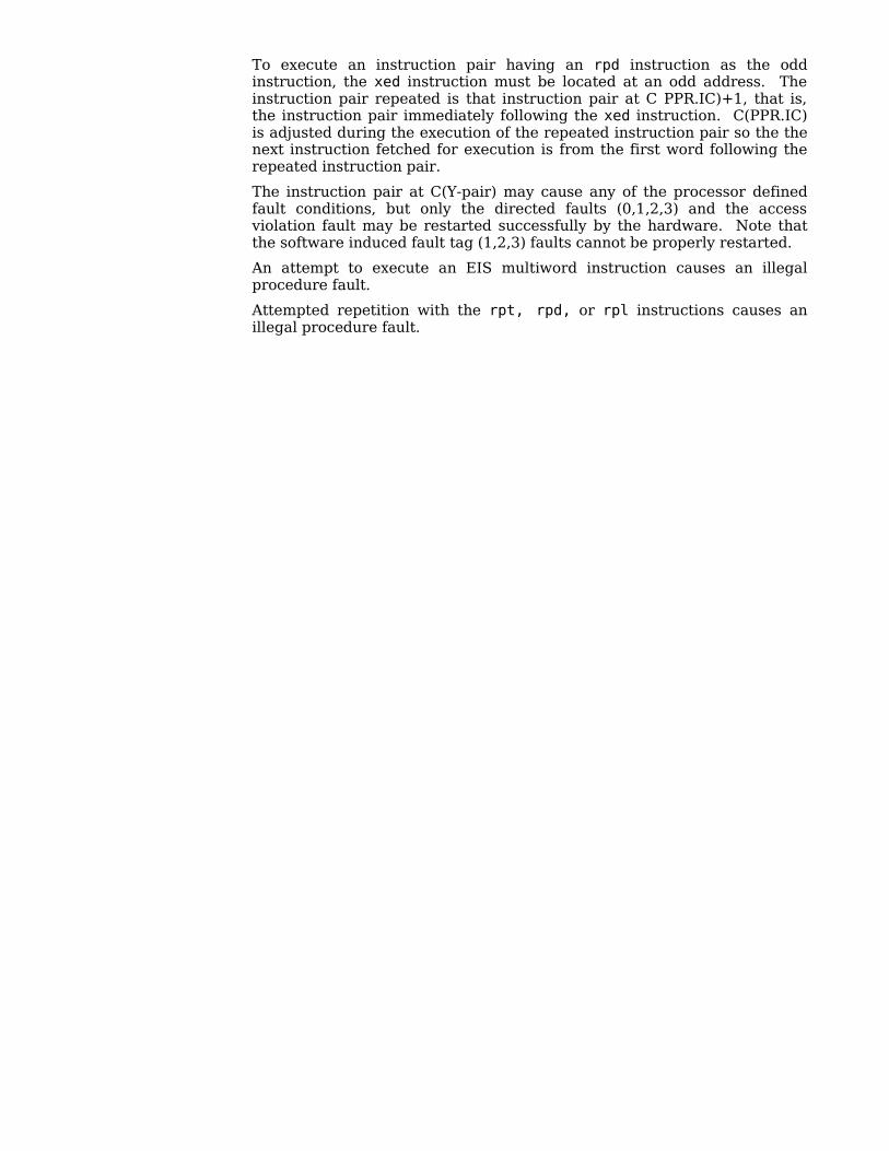
To execute an instruction pair having an rpd instruction as the odd instruction, the xed instruction must be located at an odd address. The instruction pair repeated is that instruction pair at C PPR.IC)+1, that is, the instruction pair immediately following the xed instruction. C(PPR.IC) is adjusted during the execution of the repeated instruction pair so the the next instruction fetched for execution is from the first word following the repeated instruction pair.
The instruction pair at C(Y-pair) may cause any of the processor defined fault conditions, but only the directed faults (0,1,2,3) and the access violation fault may be restarted successfully by the hardware. Note that the software induced fault tag (1,2,3) faults cannot be properly restarted.
An attempt to execute an EIS multiword instruction causes an illegal procedure fault.
Attempted repetition with the rpt, rpd, or rpl instructions causes an illegal procedure fault.
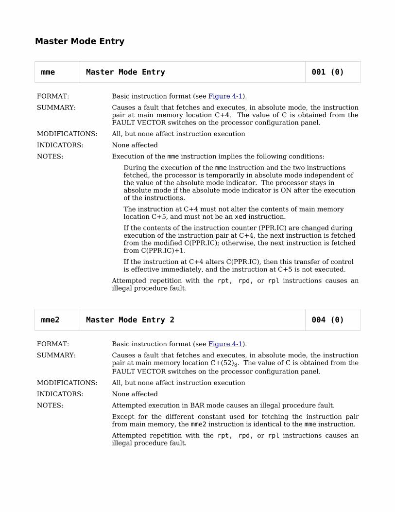
Master Mode Entry
mme Master Mode Entry 001 (0)
FORMAT: Basic instruction format (see Figure 4-1).
SUMMARY: Causes a fault that fetches and executes, in absolute mode, the instruction pair at main memory location C+4. The value of C is obtained from the FAULT VECTOR switches on the processor configuration panel.
MODIFICATIONS: All, but none affect instruction execution
INDICATORS: None affected
NOTES: Execution of the mme instruction implies the following conditions:
During the execution of the mme instruction and the two instructions fetched, the processor is temporarily in absolute mode independent of the value of the absolute mode indicator. The processor stays in absolute mode if the absolute mode indicator is ON after the execution of the instructions.
The instruction at C+4 must not alter the contents of main memory location C+5, and must not be an xed instruction.
If the contents of the instruction counter (PPR.IC) are changed during execution of the instruction pair at C+4, the next instruction is fetched from the modified C(PPR.IC); otherwise, the next instruction is fetched from C(PPR.IC)+1.
If the instruction at C+4 alters C(PPR.IC), then this transfer of control is effective immediately, and the instruction at C+5 is not executed.
Attempted repetition with the rpt, rpd, or rpl instructions causes an illegal procedure fault.
mme2 Master Mode Entry 2 004 (0)
FORMAT: Basic instruction format (see Figure 4-1).
SUMMARY: Causes a fault that fetches and executes, in absolute mode, the instruction pair at main memory location C+(52)8. The value of C is obtained from the FAULT VECTOR switches on the processor configuration panel.
MODIFICATIONS: All, but none affect instruction execution
INDICATORS: None affected
NOTES: Attempted execution in BAR mode causes an illegal procedure fault.
Except for the different constant used for fetching the instruction pair from main memory, the mme2 instruction is identical to the mme instruction.
Attempted repetition with the rpt, rpd, or rpl instructions causes an illegal procedure fault.
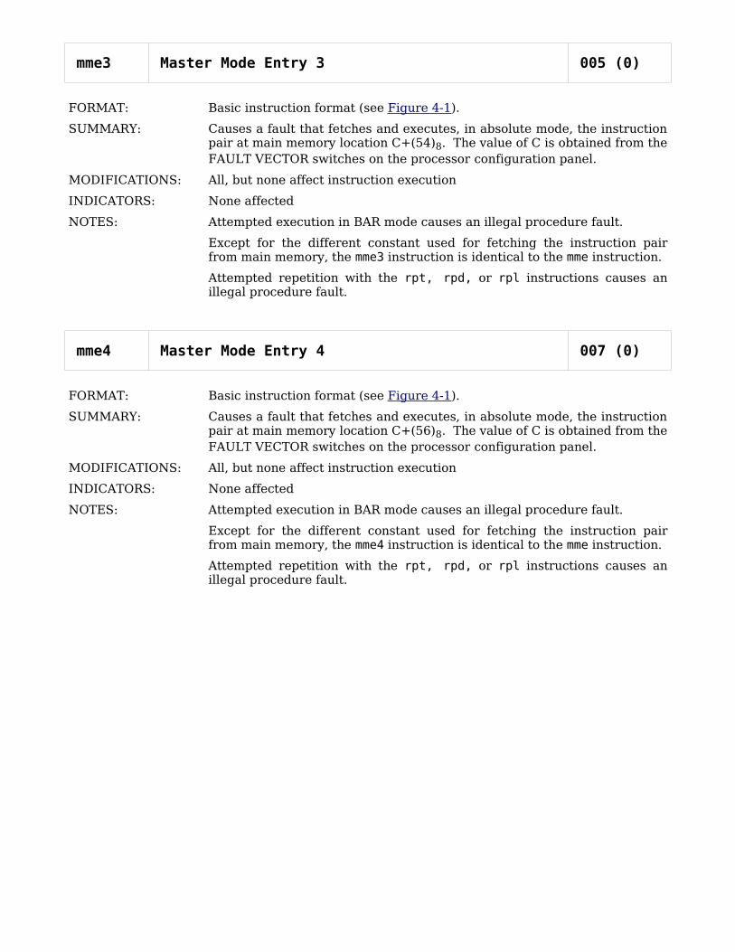
mme3 Master Mode Entry 3 005 (0)
FORMAT: Basic instruction format (see Figure 4-1).
SUMMARY: Causes a fault that fetches and executes, in absolute mode, the instruction pair at main memory location C+(54)8. The value of C is obtained from the FAULT VECTOR switches on the processor configuration panel.
MODIFICATIONS: All, but none affect instruction execution
INDICATORS: None affected
NOTES: Attempted execution in BAR mode causes an illegal procedure fault.
Except for the different constant used for fetching the instruction pair from main memory, the mme3 instruction is identical to the mme instruction.
Attempted repetition with the rpt, rpd, or rpl instructions causes an illegal procedure fault.
mme4 Master Mode Entry 4 007 (0)
FORMAT: Basic instruction format (see Figure 4-1).
SUMMARY: Causes a fault that fetches and executes, in absolute mode, the instruction pair at main memory location C+(56)8. The value of C is obtained from the FAULT VECTOR switches on the processor configuration panel.
MODIFICATIONS: All, but none affect instruction execution
INDICATORS: None affected
NOTES: Attempted execution in BAR mode causes an illegal procedure fault.
Except for the different constant used for fetching the instruction pair from main memory, the mme4 instruction is identical to the mme instruction.
Attempted repetition with the rpt, rpd, or rpl instructions causes an illegal procedure fault.
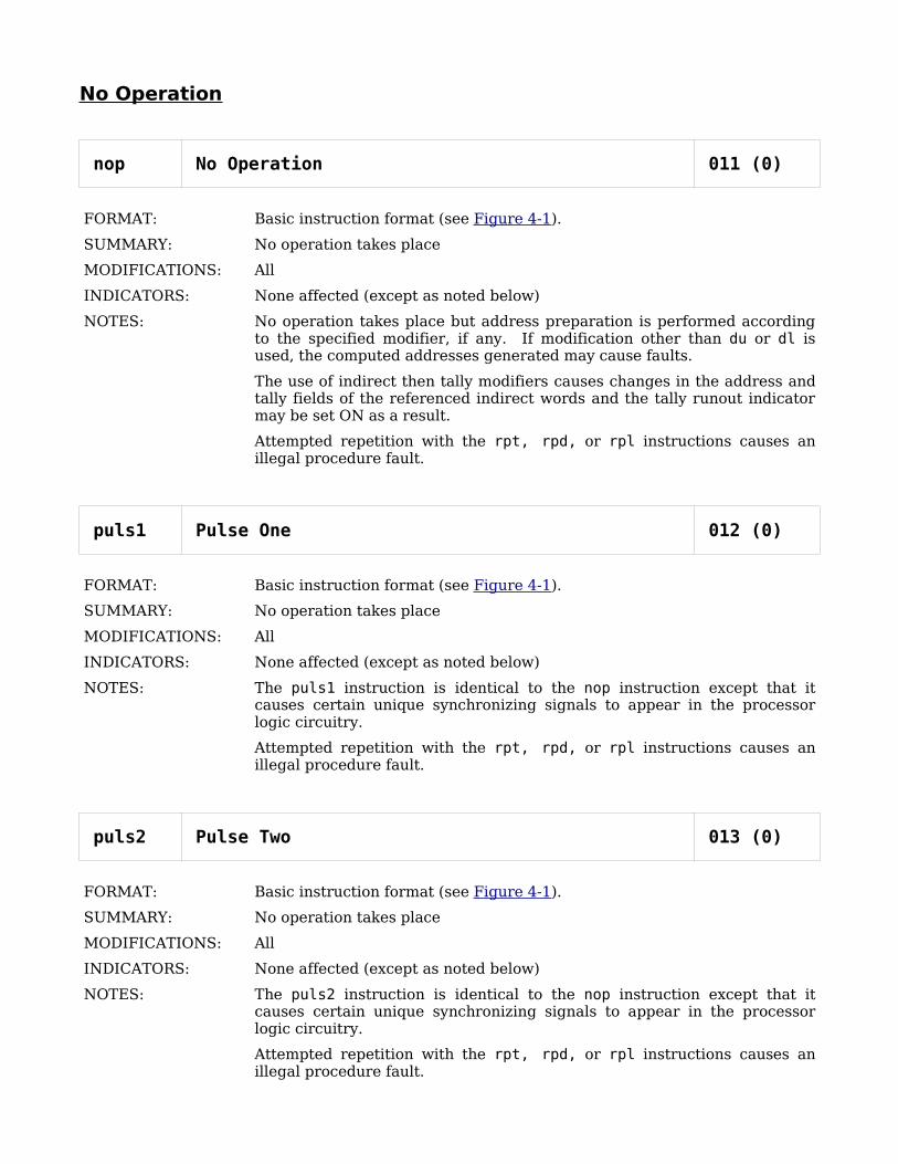
No Operation
nop No Operation 011 (0)
FORMAT: Basic instruction format (see Figure 4-1).
SUMMARY: No operation takes place
MODIFICATIONS: All
INDICATORS: None affected (except as noted below)
NOTES: No operation takes place but address preparation is performed according to the specified modifier, if any. If modification other than du or dl is used, the computed addresses generated may cause faults.
The use of indirect then tally modifiers causes changes in the address and tally fields of the referenced indirect words and the tally runout indicator may be set ON as a result.
Attempted repetition with the rpt, rpd, or rpl instructions causes an illegal procedure fault.
puls1 Pulse One 012 (0)
FORMAT: Basic instruction format (see Figure 4-1).
SUMMARY: No operation takes place
MODIFICATIONS: All
INDICATORS: None affected (except as noted below)
NOTES: The puls1 instruction is identical to the nop instruction except that it causes certain unique synchronizing signals to appear in the processor logic circuitry.
Attempted repetition with the rpt, rpd, or rpl instructions causes an illegal procedure fault.
puls2 Pulse Two 013 (0)
FORMAT: Basic instruction format (see Figure 4-1).
SUMMARY: No operation takes place
MODIFICATIONS: All
INDICATORS: None affected (except as noted below)
NOTES: The puls2 instruction is identical to the nop instruction except that it causes certain unique synchronizing signals to appear in the processor logic circuitry.
Attempted repetition with the rpt, rpd, or rpl instructions causes an illegal procedure fault.
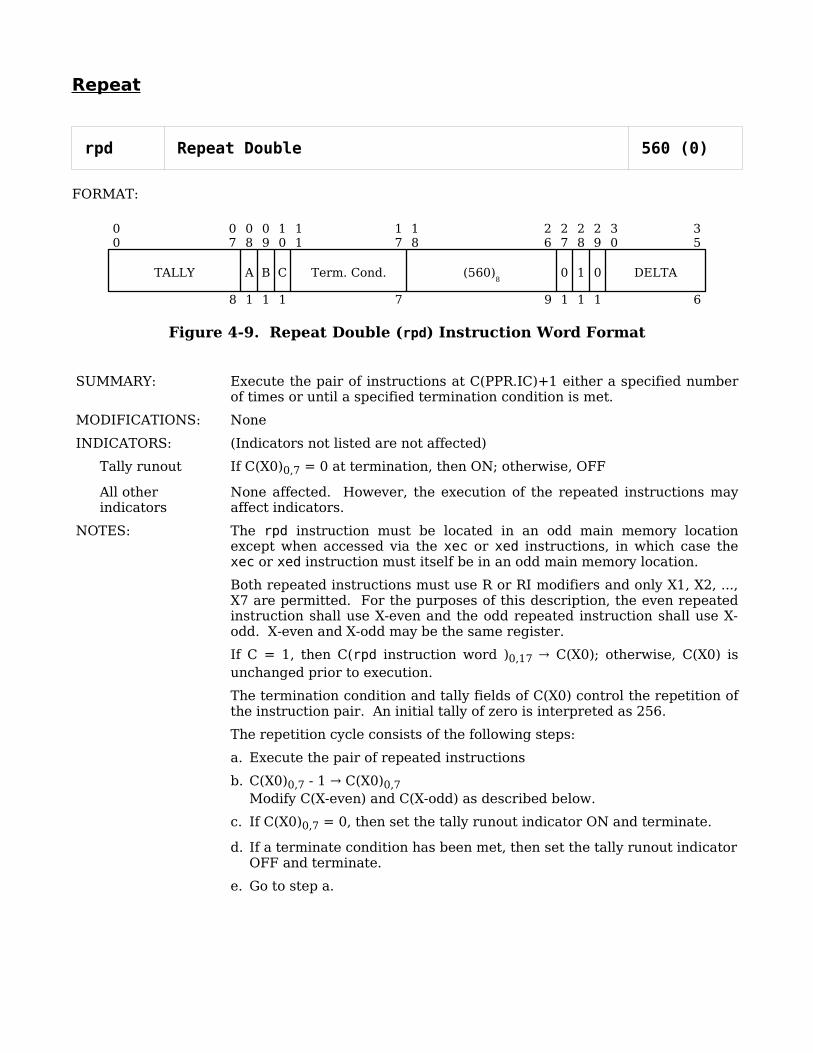
Repeat
rpd Repeat Double 560 (0)
FORMAT:
Figure 4-9. Repeat Double (rpd) Instruction Word Format
SUMMARY: Execute the pair of instructions at C(PPR.IC)+1 either a specified number of times or until a specified termination condition is met.
MODIFICATIONS: None
INDICATORS: (Indicators not listed are not affected)
Tally runout If C(X0)0,7 = 0 at termination, then ON; otherwise, OFF
All other indicators
None affected. However, the execution of the repeated instructions may affect indicators.
NOTES: The rpd instruction must be located in an odd main memory location except when accessed via the xec or xed instructions, in which case the xec or xed instruction must itself be in an odd main memory location.
Both repeated instructions must use R or RI modifiers and only X1, X2, ..., X7 are permitted. For the purposes of this description, the even repeated instruction shall use X-even and the odd repeated instruction shall use X-odd. X-even and X-odd may be the same register.
If C = 1, then C(rpd instruction word )0,17 C(X0); otherwise, C(X0) is→ unchanged prior to execution.
The termination condition and tally fields of C(X0) control the repetition of the instruction pair. An initial tally of zero is interpreted as 256.
The repetition cycle consists of the following steps:
a. Execute the pair of repeated instructions
b. C(X0)0,7 - 1 C(X0)→ 0,7Modify C(X-even) and C(X-odd) as described below.
c. If C(X0)0,7 = 0, then set the tally runout indicator ON and terminate.
d. If a terminate condition has been met, then set the tally runout indicator OFF and terminate.
e. Go to step a.
00
07
TALLY
8
08
A
1
09
B
1
10
C
1
11
17
Term. Cond.
7
18
26
(560)8
9
27
0
1
28
1
1
29
0
1
30
35
DELTA
6

If a fault occurs during the execution of the instruction pair, the repetition loop is terminated and control passes to the instruction pair associated with the fault according to the conditions for the fault. C(X0), C(X-even), and C(X-odd) are not updated for the repetition cycle in which the fault occurs. Note in particular that certain faults occurring during execution of the even instruction preclude the execution of the odd instruction for the faulting repetition cycle.
EIS multiword instructions cannot be repeated. All other instructions may be repeated except as noted for individual instructions or those that explicitly alter C(X0).
The computed addresses, y-even and y-odd, of the operands (in the case of R modification) or indirect words (in the case of RI modification) are determined as follows:
For the first execution of the repeated instruction pair:
C(C(PPR.IC)+ 1)0,17 + C(X-even) y-even, y-even C(X-even)→ →
C(C(PPR.IC)+2)0,17 + C(X-odd) y-odd, y-odd C(X-odd)→ →
For all successive executions of the repeated instruction pair:
if C(X0)8 = 1, then C(X-even) + Delta y-even,→
y-even C(X-even);→
otherwise, C(X-even) y-even→
if C(X0)9 = 1, then C(X-odd) + Delta y-odd,→
y-odd C(X-odd);→
otherwise, C(X-odd) y-odd→
C(X0)8,9 correspond to control bits A and B, respectively, of the rpd instruction word.
In the case of RI modification, only one indirect reference is made per repeated execution. The TAG field of the indirect word is not interpreted. The indirect word is treated as though it had R modification with R = N.
The bit configuration in C(X0)11,17 defines the conditions for which the repetition loop is terminated. The terminate conditions are examined at the completion of execution of the odd instruction. If more than one condition is specified, the repeat terminates if any of the specified conditions are met.
Bit 17 = 0 Ignore all overflows. Do not set the overflow indicator and inhibit the overflow fault.
Bit 17 = 1 Process overflows. If the overflow mask indicator is ON, then set the overflow indicator and terminate; otherwise, cause an overflow fault.
Bit 16 = 1 Terminate if the carry indicator is OFF.
Bit 15 = 1 Terminate if the carry indicator is ON.
Bit 14 = 1 Terminate if the negative indicator is OFF.
Bit 13 = 1 Terminate if the negative indicator is ON.
Bit 12 = 1 Terminate if the zero indicator is OFF.
Bit 11 = 1 Terminate if the zero indicator is ON.
At the time of termination:
C(X0)0,7 contain the tally residue; that is, the number of repeats remaining until a tally runout would have occurred.
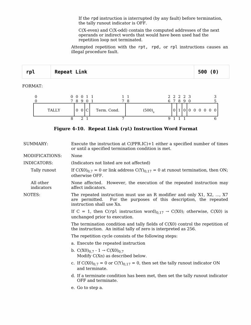
If the rpd instruction is interrupted (by any fault) before termination, the tally runout indicator is OFF.
C(X-even) and C(X-odd) contain the computed addresses of the next operands or indirect words that would have been used had the repetition loop not terminated.
Attempted repetition with the rpt, rpd, or rpl instructions causes an illegal procedure fault.
rpl Repeat Link 500 (0)
FORMAT:
Figure 4-10. Repeat Link (rpl) Instruction Word Format
SUMMARY: Execute the instruction at C(PPR.IC)+1 either a specified number of times or until a specified termination condition is met.
MODIFICATIONS: None
INDICATORS: (Indicators not listed are not affected)
Tally runout If C(X0)0,7 = 0 or link address C(Y)0,17 = 0 at runout termination, then ON; otherwise OFF.
All other indicators
None affected. However, the execution of the repeated instruction may affect indicators.
NOTES: The repeated instruction must use an R modifier and only X1, X2, ..., X7 are permitted. For the purposes of this description, the repeated instruction shall use Xn.
If C = 1, then C(rpl instruction word)0,17 C(X0); otherwise, C(X0) is→ unchanged prior to execution.
The termination condition and tally fields of C(X0) control the repetition of the instruction. An initial tally of zero is interpreted as 256.
The repetition cycle consists of the following steps:
a. Execute the repeated instruction
b. C(X0)0,7 - 1 C(X0)→ 0,7Modify C(Xn) as described below.
c. If C(X0)0,7 = 0 or C(Y)0,17 = 0, then set the tally runout indicator ON and terminate.
d. If a terminate condition has been met, then set the tally runout indicator OFF and terminate.
e. Go to step a.
00
07
TALLY
8
08
0
09
0
2
10
C
1
11
17
Term. Cond.
7
18
26
(500)8
9
27
0
1
28
1
1
29
0
1
30
0 0 0 0 0
35
0
6

If a fault occurs during the execution of the instruction, the repetition loop is terminated and control passes to the instruction pair associated with the fault according to the conditions for the fault. C(X0) and C(Xn) are not updated for the repetition cycle in which the fault occurs.
EIS multiword instructions cannot be repeated. All other instructions may be repeated except as noted for individual instructions or those that explicitly alter C(X0) or explicitly alter the link address, C(Y)0,17.
The computed address, y, of the operand is determined as follows:
For the first execution of the repeated instruction:
C(C(PPR.IC)+1)0,17 + C(Xn) y, y C(Xn)→ →
For all successive executions of the repeated instruction:
C(Xn) y→
if C(Y)0,17 ≠ 0, then C (y)0,17 C(Xn);→
otherwise, no change to C(Xn)
C(Y)0,17 is known as the link address and is the computed address of the next entry in a threaded list of operands to be referenced by the repeated instruction.
The operand is formed as:
(00...0)0,17 || C(Y)18,p
where p is 35 for single precision operands and 71 for double precision operands.
The bit configuration in C(X0)11,17 and the link address, C(Y)0,17 define the conditions for which the repetition loop is terminated. The terminate conditions are examined at the completion of execution of the instruction. If more than one condition is specified, the repeat terminates if any of the specified conditions are met.
C(Y)0,17 = 0 Set the tally runout indicator ON and terminate.
Bit 17 = 0 Ignore all overflows. Do not set the overflow indicator and inhibit the overflow fault.
Bit 17 = 1 Process overflows. If the overflow mask indicator is ON, then set the overflow indicator and terminate; otherwise, cause an overflow fault.
Bit 16 = 1 Terminate if the carry indicator is OFF.
Bit 15 = 1 Terminate if the carry indicator is ON.
Bit 14 = 1 Terminate if the negative indicator is OFF.
Bit 13 = 1 Terminate if the negative indicator is ON.
Bit 12 = 1 Terminate if the zero indicator is OFF.
Bit 11 = 1 Terminate if the zero indicator is ON.
At the time of termination:
C(X0)0,7 contain the tally residue; that is, the number of repeats remaining until a tally runout would have occurred.
If the rpl instruction is interrupted (by any fault) before termination, the tally runout indicator is OFF.
C(Xn) contain the last link address, that is, the computed address of the list word containing the last operand and the next link address.

Attempted repetition with the rpt, rpd, or rpl instructions causes an illegal procedure fault.
rpt Repeat 520 (0)
FORMAT:
Figure 4-11. Repeat (rpt) Instruction Word Format
SUMMARY: Execute the instruction at C(PPR.IC)+1 either a specified number of times or until a specified termination condition is met.
MODIFICATIONS: None
INDICATORS: (Indicators not listed are not affected)
Tally runout If C(X0)0,7 = 0 at termination, then ON; otherwise, OFF
All other indicators
None affected. However, the execution of the repeated instruction may affect indicators.
NOTES: The repeated instruction must use an R or RI modifier and only X1, X2, ..., X7 are permitted. For the purposes of this description, the repeated instruction shall use Xn.
If C = 1, then C(rpt instruction word)0,17 C(X0); otherwise, C(X0)→ unchanged prior to execution.
The termination condition and tally fields of C(X0) control the repetition of the instruction. An initial tally of zero is interpreted as 256.
The repetition cycle consists of the following steps:
a. Execute the repeated instruction
b. C(X0)0,7 - 1 C(X0)→ 0,7Modify C(Xn) as described below
c. If C(X0)0,7 = 0, then set the tally runout indicator ON and terminate
d. If a terminate condition has been met, then set the tally runout indicator OFF and terminate
e. Go to step a
If a fault occurs during the execution of the instruction, the repetition loop is terminated and control passes to the instruction pair associated with the fault according to the conditions for the fault. C(X0) and C(Xn) are not updated for the repetition cycle in which the fault occurs.
EIS multiword instructions cannot be repeated. All other instructions may be repeated except as noted for individual instructions or those that explicitly alter C(X0) or explicitly alter the instruction pair containing the repeated instruction.
The computed address, y, of the operand (in the case of R modification) or indirect word (in the case of RI modification) is determined as follows:
00
07
TALLY
8
08
0
09
0
2
10
C
1
11
17
Term. Cond.
7
18
26
(520)8
9
27
0
1
28
1
1
29
0
1
30
35
DELTA
6

For the first execution of the repeated instruction:
C(C(PPR.IC)+1)0,17 + C(Xn) y, y C(Xn)→ →
For all successive executions of the repeated instruction:
C(Xn) + Delta y, y C(Xn);→ →
In the case of RI modification, only one indirect reference is made per repeated execution. The TAG field of the indirect word is not interpreted. The indirect word is treated as though it had R modification with R = N.
The bit configuration in C(X0)11,17 defines the conditions for which the repetition loop is terminated. The terminate conditions are examined at the completion of execution of the instruction. If more than one condition is specified, the repeat terminates if any of the specified conditions are met. overflow indicator and inhibit the overflow fault.
Bit 17 = 0 Ignore all overflows. Do not set the overflow indicator and inhibit the overflow fault.
Bit 17 = 1 Process overflows. If the overflow mask indicator is ON, then set the overflow indicator and terminate; otherwise, cause an overflow fault.
Bit 16 = 1 Terminate if the carry indicator is OFF.
Bit 15 = 1 Terminate if the carry indicator is ON.
Bit 14 = 1 Terminate if the negative indicator is OFF.
Bit 13 = 1 Terminate if the negative indicator is ON.
Bit 12 = 1 Terminate if the zero indicator is OFF.
Bit 11 = 1 Terminate if the zero indicator is ON.
At the time of termination:
C(X0)0,7 contain the tally residue; that is, the number of repeats remaining until a tally runout would have occurred.
If the rpt instruction is interrupted (by any fault) before termination, the tally runout indicator is OFF.
C(Xn) contain the computed address of the next operand or indirect word that would have been used had the repetition loop not terminated.
Attempted repetition with the rpt, rpd, or rpl instructions causes an illegal procedure fault.
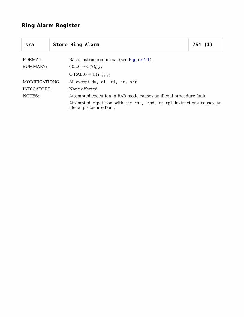
Ring Alarm Register
sra Store Ring Alarm 754 (1)
FORMAT: Basic instruction format (see Figure 4-1).
SUMMARY: 00...0 C(Y)→ 0,32
C(RALR) C(Y)→ 33,35
MODIFICATIONS: All except du, dl, ci, sc, scr
INDICATORS: None affected
NOTES: Attempted execution in BAR mode causes an illegal procedure fault.
Attempted repetition with the rpt, rpd, or rpl instructions causes an illegal procedure fault.

Store Base Address Register
sbar Store Base Address Register 550 (0)
FORMAT: Basic instruction format (see Figure 4-1).
SUMMARY: C(BAR) C(Y) → 0,17
MODIFICATIONS: All except du, dl, ci, sc, scr
INDICATORS: None affected

Translation
bcd Binary to Binary-Coded-Decimal 505 (0)
FORMAT: Basic instruction format (see Figure 4-1).
SUMMARY: Shift C(A) left three positions
| C(A) | / C(Y) 4-bit quotient plus remainder→
Shift C(Q) left six positions
4-bit quotient C(Q)→ 32,35
remainder C(A)→
MODIFICATIONS: All except ci, sc, scr
INDICATORS: (Indicators not listed are not affected)
Zero If C(A) = 0, then ON; otherwise OFF
Negative If C(A)0 = 1 before execution, then ON; otherwise OFF
NOTES: The bcd instruction carries out one step in an algorithm for the conversion of a binary number to a string of Binary-Coded-Decimal (BCD) digits. The algorithm requires the repeated short division of the binary number or last remainder by a set of constants = 8**i x 10**(n-i) for i = 1, 2, ..., n with n being defined by:
10**(n-1) <= | <binary number> | <= 10**n - 1.
The values in the table that follows are the conversion constants to be used with the bcd instruction. Each vertical column represents the set of constants to be used depending on the initial value of the binary number to be converted. The instruction is executed once per digit while traversing the appropriate column from top to bottom.
An alternate use of the table for conversion involves the use of the constants in the row corresponding to conversion step 1. If, after each execution, the contents of the accumulator are shifted right 3 positions, the constants in the first row, starting at the appropriate column, may be used while traversing the row from left to right.
Because there is a limit on range, a full 36-bit word cannot be converted. The largest binary number that may be converted correctly is 2**33 - 1 yielding ten decimal digits.
Attempted repetition with the rpl instruction causes an illegal procedure fault.
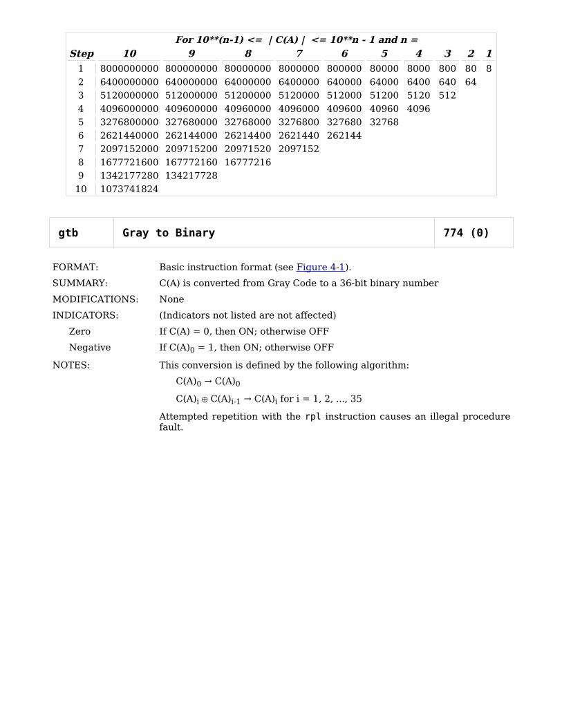
For 10**(n-1) <= | C(A) | <= 10**n - 1 and n =
Step 10 9 8 7 6 5 4 3 2 1
1 8000000000 800000000 80000000 8000000 800000 80000 8000 800 80 8
2 6400000000 640000000 64000000 6400000 640000 64000 6400 640 643 5120000000 512000000 51200000 5120000 512000 51200 5120 512
4 4096000000 409600000 40960000 4096000 409600 40960 40965 3276800000 327680000 32768000 3276800 327680 32768
6 2621440000 262144000 26214400 2621440 2621447 2097152000 209715200 20971520 2097152
8 1677721600 167772160 167772169 1342177280 134217728
10 1073741824
gtb Gray to Binary 774 (0)
FORMAT: Basic instruction format (see Figure 4-1).
SUMMARY: C(A) is converted from Gray Code to a 36-bit binary number
MODIFICATIONS: None
INDICATORS: (Indicators not listed are not affected)
Zero If C(A) = 0, then ON; otherwise OFF
Negative If C(A)0 = 1, then ON; otherwise OFF
NOTES: This conversion is defined by the following algorithm:
C(A)0 C(A)→ 0
C(A)i C(A)⊕ i-1 C(A)→ i for i = 1, 2, ..., 35
Attempted repetition with the rpl instruction causes an illegal procedure fault.

REGISTER LOAD
lbar Load Base Address Register 230 (0)
FORMAT: Basic instruction format (see Figure 4-1).
SUMMARY: C(Y)0,17 C(BAR)→
MODIFICATIONS: All except ci, sc, scr
INDICATORS: None affected
NOTES: Attempted repetition with the rpt, rpd, or rpl instructions causes an illegal procedure fault.
Attempted execution in BAR mode causes a illegal procedure fault.
PRIVILEGED INSTRUCTIONS
Privileged - Register Load
lcpr Load Central Processor Register 674 (0)
FORMAT: Basic instruction format (see Figure 4-1).
SUMMARY: Load selected register as noted
MODIFICATIONS: None. The instruction word TAG field is used for register selection as follows:
C(TAG) Data and Register(s)
02 C(Y) C(cache mode register)→
04 C(Y) C(mode register)→
03 DPS/L68 processors:
00...0 C(CU, OU, DU, and APU history register)→ 0,71
DPS 8M processors:
00...0 C(CU, OU/DU, APU #1 and APU #2 history→ register)0,71
07 DPS/L68 processors:
11...1 C(CU, OU, DU, and APU history register)→ 0,71
DPS 8M processors:
11...1 C(CU, OU/DU, APU #1 and APU #2 history→ register)0,71
INDICATORS: None affected
NOTES: See Section 3 for descriptions and use of the various registers.
For TAG values 03 and 07, the history register loaded is selected by the current value of a cyclic counter for each unit. All four cyclic counters are advanced by one count for each execution of the instruction.
Use of TAG values other than those defined above causes an illegal procedure fault.
Attempted execution in normal or BAR modes causes a illegal procedure fault.
Attempted repetition with the rpt, rpd, or rpl instructions causes an illegal procedure fault.
ldbr Load Descriptor Segment Base Register 232 (0)
FORMAT: Basic instruction format (see Figure 4-1).
SUMMARY: If SDWAM is enabled, then
0 C(SDWAM(i).FULL) for i = 0, 1, ..., 15→
i C(SDWAM(i).USE) for i = 0, 1, ..., 15→
If PTWAM is enabled, then
0 C(PTWAM(i).FULL) for i = 0, 1, ..., 15→
i C(PTWAM(i).USE) for i = 0, 1, ..., 15→
If cache is enabled, reset all cache column and level full flags
C(Y-pair)0,23 C(DSBR.ADDR)→
C(Y-pair)37,50 C(DSBR.BOUND)→
C(Y-pair)55 C(DSBR.U)→
C(Y-pair)60,71 C(DSBR.STACK)→
MODIFICATIONS: All except du, dl, ci, sc, scr
INDICATORS: None affected
NOTES: The associative memories and cache are cleared (full indicators reset) if they are enabled.
See Section 3 and Section 5 for descriptions and use of the SDWAM, PTWAM, and DSBR
Attempted execution in normal or BAR modes causes an illegal procedure fault.
Attempted repetition with the rpt, rpd, or rpl instructions causes an illegal procedure fault.
ldt Load Timer Register 637 (0)
FORMAT: Basic instruction format (see Figure 4-1).
SUMMARY: C(Y)0,26 C(TR)→
MODIFICATIONS: All except ci, sc, scr
INDICATORS: None affected
NOTES: Attempted execution in normal or BAR modes causes a illegal procedure fault.
Attempted repetition with the rpt, rpd, or rpl instructions causes an illegal procedure fault.
lptp Load Page Table Pointers 257 (1)
FORMAT: Basic instruction format (see Figure 4-1).
SUMMARY: For i = 0, 1, ..., 15
m = C(PTWAM(i).USE)
C(Y-block16+m)0,14 C(PTWAM(m).POINTER)→
C(Y-block16+m)15,26 C(PTWAM(m).PAGE)→
C(Y-block16+m)27 C(PTWAM(m).F)→
MODIFICATIONS: All except du, dl, ci, sc, scr
INDICATORS: None affected
NOTES: The associative memory is ignored (forced to "no match") during address preparation.
See Section 3 and Section 5 for description and use of the PTWAM.
This instruction is not available on the DPS 8M processor and attempted execution on a DPS 8M processor causes an illegal procedure fault.
Attempted execution in normal or BAR modes causes an illegal procedure fault.
Attempted repetition with the rpt, rpd, or rpl instructions causes an illegal procedure fault.
lptr Load Page Table Registers 173 (1)
FORMAT: Basic instruction format (see Figure 4-1).
SUMMARY: For i = 0, 1, ..., 15
m = C(PTWAM(i).USE)
C(Y-block16+m)0,17 C(PTWAM(m).ADDR)→
C(Y-block16+m)29 C(PTWAM(m).M)→
MODIFICATIONS: All except du, dl, ci, sc, scr
INDICATORS: None affected
NOTES: The associative memory is ignored (forced to "no match") during address preparation.
See Section 3 and Section 5 for description and use of the PTWAM.
Attempted execution in normal or BAR modes causes an illegal procedure fault.
This instruction is not available on the DPS 8M processor and attempted execution on a DPS 8M processor produces an illegal procedure fault.
Attempted repetition with the rpt, rpd, or rpl instructions causes an illegal procedure fault.
lra Load Ring Alarm Register 774 (1)
FORMAT: Basic instruction format (see Figure 4-1).
SUMMARY: C(Y)33,35 C(RALR)→
MODIFICATIONS: All except du, dl, ci, sc, scr

INDICATORS: None affected
NOTES: Attempted execution in normal or BAR modes causes an illegal procedure fault.
Attempted repetition with the rpt, rpd, or rpl instructions causes an illegal procedure fault.
lsdp Load Segment Descriptor Pointers 257 (0)
FORMAT: Basic instruction format (see Figure 4-1).
SUMMARY: For i = 0, 1, ..., 15
m = C(SDWAM(i).USE)
C(Y-block16+m)0,14 C(SDWAM(m).POINTER)→
C(Y-block16+m)17 C(SDWAM(m).P)→
MODIFICATIONS: All except du, dl, ci, sc, scr
INDICATORS: None affected
NOTES: The associative memory is ignored (forced to "no match") during address preparation.
See Section 3 and Section 5 for description and use of the SDWAM.
This instruction is not available on the DPS 8M processor and attempted execution on a DPS 8M processor produces an illegal procedure fault.
Attempted execution in normal or BAR modes causes an illegal procedure fault.
Attempted repetition with the rpt, rpd, or rpl instructions causes an illegal procedure fault.
lsdr Load Segment Descriptor Registers 232 (1)
FORMAT: Basic instruction format (see Figure 4-1).
SUMMARY: For i = 0, 1, ..., 15
m = C(SDWAM(i).USE)
Y-pair = Y-block32 + 2m
C(Y-pair)0,23 C(SDWAM(m).ADDR)→
C(Y-pair)24,32 C(SDWAM(m).R1, R2, R3)→
C(Y-pair)37,50 C(SDWAM(m).BOUND)→
C(Y-pair)52,57 C(SDWAM(m).R, E, W, P, U, G, C)→
C(Y-pair)58,71 C(SDWAM(m).CL)→
MODIFICATIONS: All except du, dl, ci, sc, scr
INDICATORS: None affected
NOTES: The associative memory is ignored (forced to "no-match") during address preparation.
See Section 3 and Section 5 for description and use of the SDWAM.
This instruction is not available on the DPS 8M processor and attempted execution on a DPS 8M processor produces an illegal procedure fault.
Attempted execution in normal or BAR modes causes an illegal procedure fault.
Attempted repetition with the rpt, rpd, or rpl instructions causes an illegal procedure fault.
rcu Restore Control Unit 613 (0)
FORMAT: Basic instruction format (see Figure 4-1).
SUMMARY: C(Y-block8) words 0 to 7 (control unit data)→
MODIFICATIONS: All except du, dl, ci, sc, scr
INDICATORS: None affected
NOTES: See Section 3 for description and use of control unit data.
Attempted execution in normal or BAR modes causes an illegal procedure fault.
Attempted repetition with the rpt, rpd, or rpl instructions causes an illegal procedure fault.

Privileged - Register Store
scpr Store Central Processor Register 452 (0)
FORMAT: Basic instruction format (see Figure 4-1).
SUMMARY: Store selected register as noted
MODIFICATIONS: None. The instruction word TAG field is used for register selection word as follows:
C(TAG) MEANING
00 DPS/L68 processor:
C(APU history register) C(Y-pair)→
DPS 8M processor:
C(APU history register #1) C(Y-pair)→
01 C(fault register) C(Y-pair)→ 0,35
00...0 C(Y-pair)→ 36,71
06 C(mode register) C(Y-pair)→ 0,35
C(cache mode register) C(Y-pair)→ 36,71
10 DPS/L68 processor:
C(DU history register) C(Y-pair)→
DPS 8M processor:
C(APU history register #2) C(Y-pair)→
20 C(CU history register) C(Y-pair)→
40 DPS/L68 processor
C(OU history register) C(Y-pair)→
DPS 8M processor:
C(OU/DU history register) C(Y-pair)→
INDICATORS: None affected
NOTES: See Section 3 for description and use of the various registers.
The TAG field values shown are octal.
For TAG values 00, 10, 20, and 40, the history register stored is selected by the current value of a cyclic counter for each unit. The individual cyclic counters are advanced by one count for each execution of the instruction.
The use of TAG values other than those defined above causes an illegal procedure fault.
Attempted execution in normal or BAR modes causes an illegal procedure fault.
Attempted repetition with the rpt, rpd, or rpl instructions causes an illegal procedure fault.

scu Store Control Unit 657 (0)
FORMAT: Basic instruction format (see Figure 4-1).
SUMMARY: (control unit data) C(Y-block8)→
MODIFICATIONS: All except du, dl, ci, sc, scr
INDICATORS: None affected
NOTES: See Section 3 for description and use of control unit data.
The scu instruction safe-stores control information required to service a fault or interrupt. The control unit data is not, in general, valid at any time except when safe-stored by the first of the pair of instructions associated with the fault or interrupt.
Attempted execution in normal or BAR modes causes an illegal procedure fault.
Attempted repetition with the rpt, rpd, or rpl instructions causes an illegal procedure fault.
sdbr Store Descriptor Segment Base Register 154 (0)
FORMAT: Basic instruction format (see Figure 4-1).
SUMMARY: C(DSBR.ADDR) C(Y-pair)→ 0,23
00...0 C(Y-pair)→ 24,36
C(DSBR.BOUND) C(Y-pair)→ 37,50
0000 C(Y-pair)→ 51,54
C(DSBR.U) C(Y-pair)→ 55
000 C(Y-pair)→ 56,59
C(DSBR.STACK) C(Y-pair)→ 60,71
MODIFICATIONS: All except du, dl, ci, sc, scr
INDICATORS: None affected
NOTES: C(DSBR) are unchanged.
See Section 3 and Section 5 for description and use of the DSBR
Attempted execution in normal or BAR modes causes an illegal procedure fault.
Attempted repetition with the rpt, rpd, or rpl instructions causes an illegal procedure fault.
sptp Store Page Table Pointers 557 (1)
FORMAT: Basic instruction format (see Figure 4-1).
SUMMARY: DPS/L68 processors:
For i = 0, 1, ..., 15
C(PTWAM(i).POINTER) C(Y-block16+i)→ 0,14
C(PTWAM(i).PAGE) C(Y-block16+i)→ 15,26
C(PTWAM(i).F) C(Y-block16+i)→ 27
0000 C(Y-block16+i)→ 8,31
C(PTWAM(i).USE) C(Y-block16+i)→ 32,35
DPS 8M processors:
This instruction stores 16 words from the selected level (j) of the directory of the Page Table Word associative memory. There are four levels.
Level j is selected by C(TPR.CA)12,13
For i = 0, 1, ..., 15
C(PTWAM(i,j).POINTER) C(Y-block16+i)→ 0,14
C(PTWAM(i,j).PAGENO) C(Y-block16+i)→ 15,22
0000 C(Y-block16+i)→ 23,26
C(PTWAM(i,j).F) C(Y-block16+i)→ 27
00 C(Y-block16+i)→ 28,29
C(PTWAM(i,j).LRU) C(Y-block16+i)→ 30,35
MODIFICATIONS: All except du, dl, ci, sc, scr
INDICATORS: None affected
NOTES: The contents of the associative memory remain unchanged.
The associative memory is ignored (forced to "no match") during address preparation.
See Section 3 and Section 5 for description and use of the PTWAM.
Attempted execution in normal or BAR modes causes an illegal procedure fault.
Attempted repetition with the rpt, rpd, or rpl instructions causes an illegal procedure fault.
sptr Store Page Table Registers 154 (1)
FORMAT: Basic instruction format (see Figure 4-1).
SUMMARY: DPS/L68 processors:
For i = 0, 1, ..., 15
C(PTWAM(i).ADDR) C(Y-block16+i)→ 0,17
00...0 C(Y-block16+i)→ 18,28
C(PTWAM(i).M) C(Y-block16+i)→ 29
00...0 C(Y-block16+i)→ 30,35
DPS 8M processors:

This instruction stores 16 words from the selected level (j) of the contents of the Page Table Word associative memory. There are four levels.
Level j is selected by C(TPR.CA)12,13
For i = 0, 1, ..., 15
C(PTWAM(i,j).PAGE ADDR) C(Y-block16+1)→ 0,13
00...0 C(Y-block16+i)→ 14,28
C(PTWAM(i,j).M C(Y-block16+i)→ 29
000000 C(Y-block16+i)→ 30,3
MODIFICATIONS: All except du, dl, ci, sc, scr
INDICATORS: None affected
NOTES: The contents of the associative memory are unchanged.
The associative memory is ignored (forced to "no match") during address preparation.
See Section 3 and Section 5 for description and use of the PTWAM.
Attempted execution in normal or BAR modes causes an illegal procedure fault.
Attempted repetition with the rpt, rpd, or rpl instructions causes an illegal procedure fault.
ssdp Store Segment Descriptor Pointers 557 (0)
FORMAT: Basic instruction format (see Figure 4-1).
SUMMARY: DPS/L68 processors:
For i = 0, 1, ..., 15
C(SDWAM(i).POINTER) C(Y-block16+i)→ 0,14
00...0 C(Y-block16+i)→ 15,26
C(SDWAM(i).F) C(Y-block16+i)→ 27
0000 C(Y-block16+i)→ 28,31
C(SDWAM(i).USE) C(Y-block16+i)→ 32,35
DPS 8M processors:
This instruction stores 16 words from the selected level (j) of the directory of the Segment Descriptor Word associative memory. There are four levels.
Level j is selected by C(TPR.CA)12,13
For i = 0, 1, ..., 15
C(SDWAM(i,j).POINTER) C(Y-block16+i)→ 0,14
00...0 C(Y-block16+i)→ 15,26
C(SDWAM(i,j).F) C(Y-block16+i)→ 27
00 C(Y-block16+i)→ 28,29
C(SDWAM(i,j).LRU) C(Y-block16+i)→ 30,35
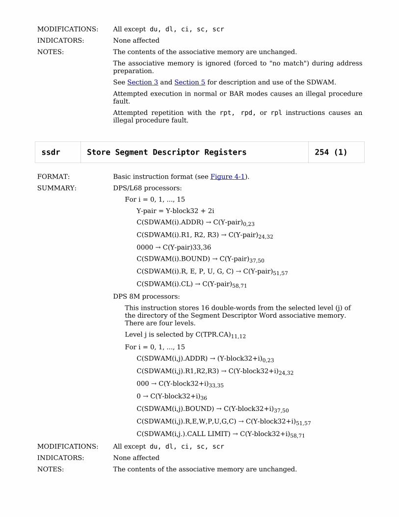
MODIFICATIONS: All except du, dl, ci, sc, scr
INDICATORS: None affected
NOTES: The contents of the associative memory are unchanged.
The associative memory is ignored (forced to "no match") during address preparation.
See Section 3 and Section 5 for description and use of the SDWAM.
Attempted execution in normal or BAR modes causes an illegal procedure fault.
Attempted repetition with the rpt, rpd, or rpl instructions causes an illegal procedure fault.
ssdr Store Segment Descriptor Registers 254 (1)
FORMAT: Basic instruction format (see Figure 4-1).
SUMMARY: DPS/L68 processors:
For i = 0, 1, ..., 15
Y-pair = Y-block32 + 2i
C(SDWAM(i).ADDR) C(Y-pair)→ 0,23
C(SDWAM(i).R1, R2, R3) C(Y-pair)→ 24,32
0000 C(Y-pair)33,36→
C(SDWAM(i).BOUND) C(Y-pair)→ 37,50
C(SDWAM(i).R, E, P, U, G, C) C(Y-pair)→ 51,57
C(SDWAM(i).CL) C(Y-pair)→ 58,71
DPS 8M processors:
This instruction stores 16 double-words from the selected level (j) of the directory of the Segment Descriptor Word associative memory. There are four levels.
Level j is selected by C(TPR.CA)11,12
For i = 0, 1, ..., 15
C(SDWAM(i,j).ADDR) (Y-block32+i)→ 0,23
C(SDWAM(i,j).R1,R2,R3) C(Y-block32+i)→ 24,32
000 C(Y-block32+i)→ 33,35
0 C(Y-block32+i)→ 36
C(SDWAM(i,j).BOUND) C(Y-block32+i)→ 37,50
C(SDWAM(i,j).R,E,W,P,U,G,C) C(Y-block32+i)→ 51,57
C(SDWAM(i,j.).CALL LIMIT) C(Y-block32+i)→ 58,71
MODIFICATIONS: All except du, dl, ci, sc, scr
INDICATORS: None affected
NOTES: The contents of the associative memory are unchanged.

The associative memory is ignored (forced to "no match") during address preparation.
See Section 3 and Section 5 for description and use of the SDWAM.
Attempted execution in normal or BAR modes causes an illegal procedure fault.
Attempted repetition with the rpt, rpd, or rpl instructions causes an illegal procedure fault.

Privileged - Clear Associative Memory
camp Clear Associative Memory Pages 532 (1)
FORMAT: Basic instruction format (see Figure 4-1).
SUMMARY: DPS/L68 processors:
For i = 0, 1, ..., 15
0 C(PTWAM(i).F)→
(i) C(PTWAM(i).USE)→
DPS 8M processors:
If the associative memory is enabled
0 C(PTWAM.F)→
C(PTWAM.LRU) is initialized for all PTWAM registers
MODIFICATIONS: All except du, dl, ci, sc, scr
INDICATORS: None affected
NOTES: DPS/L68 processors:
The full/empty bit of each PTWAM register is set to 0, and the usage counters (PTWAM.USE) are set to their pre-assigned values of 0 through 15. The remainder of C PTWAM(i)) is unchanged .
The execution of this instruction enables the PTWAM if it is disabled and C(TPR.CA)16,17 = 10.
The execution of this instruction disables the PTWAM if C(TPR.CA)16,17 = 01.
If C(TPR.CA)15 = 1, a selective clear of cache is executed. Any cache block for which the upper 14 bits of the directory entry equal C(PTWAM(i).ADDR)0,13 will have its full/empty bit set to empty.
DPS 8M processors:
The full/empty bit of cache PTWAM register is set to zero and the LRU counters are initialized. The remainder of the contents of the registers are unchanged. If the associative memory is disabled, F and LRU are unchanged.
C(TPR.CA)16,17 control disabling or enabling the associative memory. This may be done to either or both halves.
C(TPR.CA)13,14 Selection
00 both halves
01 lower half, levels C & D
10 upper half, levels A & B
11 both halves
The selected portion of the associative memory is
-disabled if C(TPR.CA)16,17 = 01
-enabled if C(TPR.CA)16,17 = 10
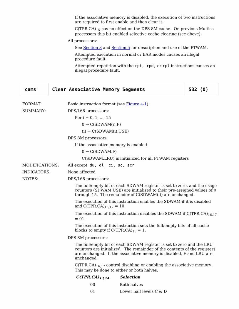
If the associative memory is disabled, the execution of two instructions are required to first enable and then clear it.
C(TPR.CA)15 has no effect on the DPS 8M cache. On previous Multics processors this bit enabled selective cache clearing (see above).
All processors:
See Section 3 and Section 5 for description and use of the PTWAM.
Attempted execution in normal or BAR modes causes an illegal procedure fault.
Attempted repetition with the rpt, rpd, or rpl instructions causes an illegal procedure fault.
cams Clear Associative Memory Segments 532 (0)
FORMAT: Basic instruction format (see Figure 4-1).
SUMMARY: DPS/L68 processors:
For i = 0, 1, ..., 15
0 C(SDWAM(i).F)→
(i) C(SDWAM(i).USE)→
DPS 8M processors:
If the associative memory is enabled
0 C(SDWAM.F)→
C(SDWAM.LRU) is initialized for all PTWAM registers
MODIFICATIONS: All except du, dl, ci, sc, scr
INDICATORS: None affected
NOTES: DPS/L68 processors:
The full/empty bit of each SDWAM register is set to zero, and the usage counters (SDWAM.USE) are initialized to their pre-assigned values of 0 through 15. The remainder of C(SDWAM(i)) are unchanged.
The execution of this instruction enables the SDWAM if it is disabled and C(TPR.CA)16,17 = 10.
The execution of this instruction disables the SDWAM if C(TPR.CA)16,17 = 01.
The execution of this instruction sets the full/empty bits of all cache blocks to empty if C(TPR.CA)15 = 1.
DPS 8M processors:
The full/empty bit of each SDWAM register is set to zero and the LRU counters are initialized. The remainder of the contents of the registers are unchanged. If the associative memory is disabled, F and LRU are unchanged.
C(TPR.CA)16,17 control disabling or enabling the associative memory. This may be done to either or both halves.
C(TPR.CA)13,14 Selection
00 Both halves
01 Lower half levels C & D

C(TPR.CA)13,14 Selection
10 Upper half, levels A & B
11 Both halves
The selected portion of the associative memory is
-disabled if C(TPR.CA)16,17 = 01
-enabled if C(TPR.CA)16,17 = 10
If the associative memory is disabled, the execution of two instructions are required to first enable and then clear it.
C(TPR.CA)15 has no effect on the DPS 8M cache. On previous Multics processors this bit enabled a full cache clear (see above).
All processors:
See Section 3 and Section 5 for description and use of the SDWAM.
Attempted execution in normal or BAR modes causes an illegal procedure fault.
Attempted repetition with the rpt, rpd, or rpl instructions causes an illegal procedure fault.
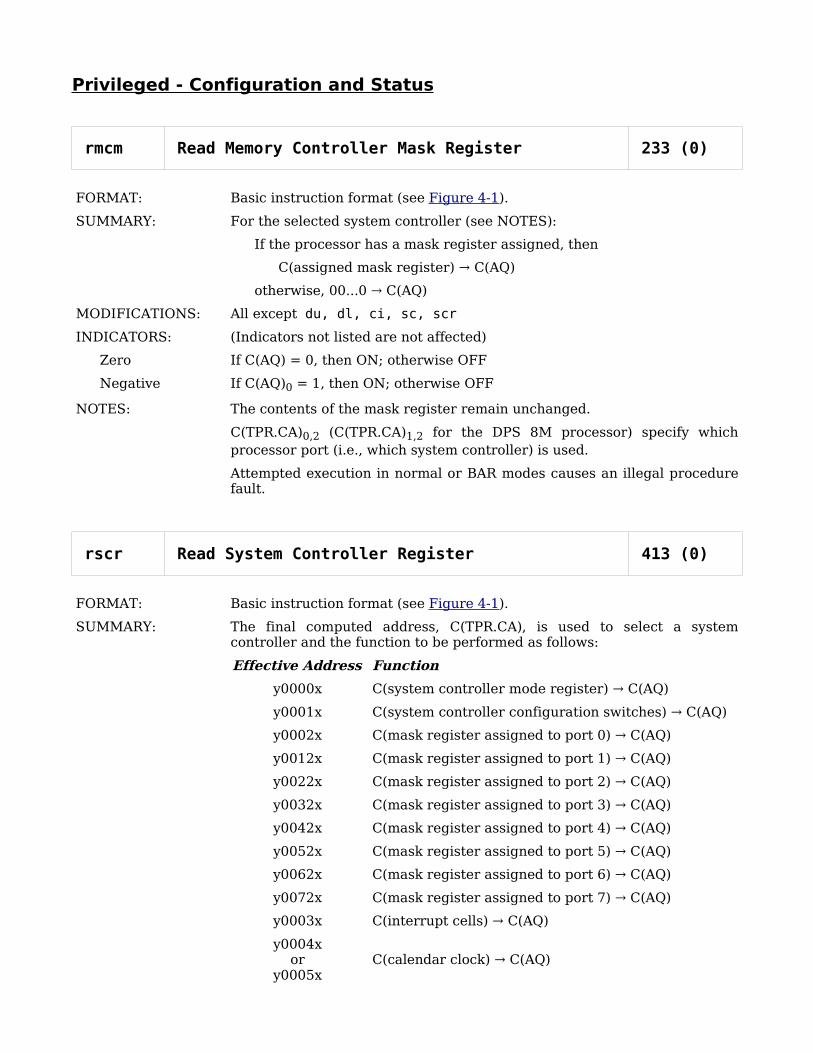
Privileged - Configuration and Status
rmcm Read Memory Controller Mask Register 233 (0)
FORMAT: Basic instruction format (see Figure 4-1).
SUMMARY: For the selected system controller (see NOTES):
If the processor has a mask register assigned, then
C(assigned mask register) C(AQ)→
otherwise, 00...0 C(AQ)→
MODIFICATIONS: All except du, dl, ci, sc, scr
INDICATORS: (Indicators not listed are not affected)
Zero If C(AQ) = 0, then ON; otherwise OFF
Negative If C(AQ)0 = 1, then ON; otherwise OFF
NOTES: The contents of the mask register remain unchanged.
C(TPR.CA)0,2 (C(TPR.CA)1,2 for the DPS 8M processor) specify which processor port (i.e., which system controller) is used.
Attempted execution in normal or BAR modes causes an illegal procedure fault.
rscr Read System Controller Register 413 (0)
FORMAT: Basic instruction format (see Figure 4-1).
SUMMARY: The final computed address, C(TPR.CA), is used to select a system controller and the function to be performed as follows:
Effective Address Function
y0000x C(system controller mode register) C(AQ)→
y0001x C(system controller configuration switches) C(AQ)→
y0002x C(mask register assigned to port 0) C(AQ)→
y0012x C(mask register assigned to port 1) C(AQ)→
y0022x C(mask register assigned to port 2) C(AQ)→
y0032x C(mask register assigned to port 3) C(AQ)→
y0042x C(mask register assigned to port 4) C(AQ)→
y0052x C(mask register assigned to port 5) C(AQ)→
y0062x C(mask register assigned to port 6) C(AQ)→
y0072x C(mask register assigned to port 7) C(AQ)→
y0003x C(interrupt cells) C(AQ)→
y0004xor
y0005xC(calendar clock) C(AQ)→

Effective Address Function
y0006xor
y0007xC(store unit mode register) C(AQ)→
where: y = value of C(TPR.CA)0,2 (C(TPR.CA)1,2 for the DPS 8M processor) used to select the system controller
x = any octal digit
MODIFICATIONS: All except du, dl, ci, sc, scr
INDICATORS: None affected
NOTES: See Section 3 for description and use of the various registers.
For computed addresses y0006x and y0007x, store unit selection is done by the normal address decoding function of the system controller.
Attempted execution in normal or BAR modes causes an illegal procedure fault.
Attempted repetition with the rpl instruction causes an illegal procedure fault.
rsw Read Switches 231 (0)
FORMAT: Basic instruction format (see Figure 4-1).
SUMMARY: The final computed address, C(TPR.CA), is used to select certain processor switches whose settings are read into the A-register.
The switches selected are as follows:
Effective Address Function
xxxxx0 C(data switches) C(A)→
xxxxxl C(configuration switches for ports A, B, C, D)
C(A)→
xxxxx2 DPS/L68 processors:
00...0 C(A)→ 0,5
C(fault base switches) C(A)→ 6,12
00...0 C(A)→ 13,22
C(processor ID) C(A )→ 23,33
C(processor number switches) C(A)→ 34,35
DPS 8M processors:
C(Port interface, Ports A-D) C(A)→ 0,3
01 C(A)→ 4,5
C(Fault base switches) C(A)→ 6,12
1 C(A)→ 13
0000 C(A)→ 14,17
111 C(A)→ 18,20
00 C(A)→ 21,22
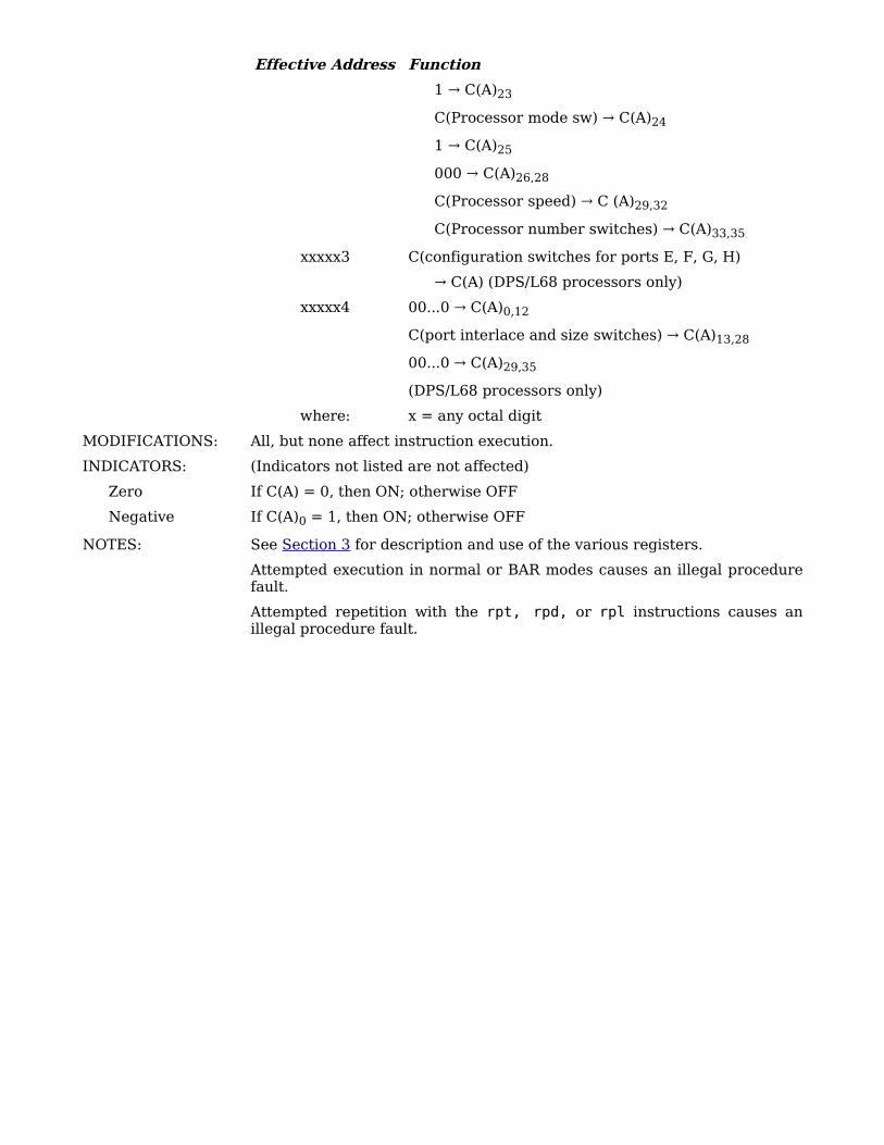
Effective Address Function
1 C(A)→ 23
C(Processor mode sw) C(A)→ 24
1 C(A)→ 25
000 C(A)→ 26,28
C(Processor speed) C (A)→ 29,32
C(Processor number switches) C(A)→ 33,35
xxxxx3 C(configuration switches for ports E, F, G, H)
C(A) (DPS/L68 processors only)→
xxxxx4 00...0 C(A)→ 0,12
C(port interlace and size switches) C(A)→ 13,28
00...0 C(A)→ 29,35
(DPS/L68 processors only)
where: x = any octal digit
MODIFICATIONS: All, but none affect instruction execution.
INDICATORS: (Indicators not listed are not affected)
Zero If C(A) = 0, then ON; otherwise OFF
Negative If C(A)0 = 1, then ON; otherwise OFF
NOTES: See Section 3 for description and use of the various registers.
Attempted execution in normal or BAR modes causes an illegal procedure fault.
Attempted repetition with the rpt, rpd, or rpl instructions causes an illegal procedure fault.

Privileged – System Control
cioc Connect I/O Channel 015 (0)
FORMAT: Basic instruction format (see Figure 4-1).
SUMMARY: The system controller addressed by Y (i.e., contains the word at Y) sends a connect signal to the port specified by C(Y)33,35.
MODIFICATIONS: All except du, dl, ci, sc, scr
INDICATORS: None affected
NOTES: Attempted execution in normal or BAR modes causes an illegal procedure fault.
Attempted repetition with the rpt, rpd, or rpl instructions causes an illegal procedure fault.
smcm Set Memory Controller Mask Register 553 (0)
FORMAT: Basic instruction format (see Figure 4-1).
SUMMARY: For the selected system controller:
If the processor has a mask register assigned, then
C(AQ) C(assigned mask register)→
otherwise a store fault (not control) occurs.
MODIFICATIONS: All except du, dl, ci, sc, scr
INDICATORS: None affected
NOTES: C(TPR.CA)0,2 (C(TPR.CA)1,2 on the DPS 8M processor) specify which processor port (i.e., which system controller) is used.
Attempted execution in normal or BAR modes causes an illegal procedure fault.
Attempted repetition with the rpl instruction causes an illegal procedure fault.
If the SCU is a 4MW type SCU, the illegal action code 1000 (Not Control Port) is not used.
smic Set Memory Controller interrupt Cells 451 (0)
FORMAT: Basic instruction format (see Figure 4-1).
SUMMARY: For i = 0, 1, ..., 15 and C(A)35 = 0:
if C(A)i = 1, then set interrupt cell i ON
For i = 0, 1, ..., 15 and C(A)35 = 1:
if C(A)i = 1, then set interrupt cell 16+i ON

MODIFICATIONS: All except du, dl, ci, sc, scr
INDICATORS: None affected
NOTES: C(TPR.CA)0,2 (C(TPR.CA)1,2 on a DPS 8M processor) specify which processor port (i.e., which system controller) is used.
If the processor has no assigned mask register in the selected system controller, a store fault (not control) occurs.
If the SCU is a 4MW type SCU, the illegal action code 1000 (Not Control Port) is not used.
Attempted execution in normal or BAR modes causes an illegal procedure fault.
sscr Set System Controller Register 057 (0)
FORMAT: Basic instruction format (see Figure 4-1).
SUMMARY: The final computed address, C(TPR.CA), is used to select a system controller and the function to be performed as follows:
Effective Address Function
y0000x C(AQ) C(system controller mode register)→
y0001x C(AQ) system controller configuration register→ (4WM SCU only)
y0002x C(AQ) C(mask register assigned to port 0)→
y0012x C(AQ) C(mask register assigned to port 1)→
y0022x C(AQ) C(mask register assigned to port 2)→
y0032x C(AQ) C(mask register assigned to port 3)→
y0042x C(AQ) C(mask register assigned to port 4)→
y0052x C(AQ) C(mask register assigned to port 5)→
y0062x C(AQ) C(mask register assigned to port 6)→
y0072x C(AQ) C(mask register assigned to port 7)→
y0003x C(AQ)0,15 C(interrupt cells 0-15)→C(AQ)36,51 C(interrupt cells 16-31)→
y0004xor
y0005x
C(AQ) (calendar clock)→(for 4MW SCU only)
y0006xor
y0007xC(AQ) C(store unit mode register)→
where: y = value of C(TPR.CA)0,2 (C(TPR.CA)1,2 on the DPS 8M processor) used to select the system controller
x = any octal digit
MODIFICATIONS: All except du, dl, ci, sc, scr
INDICATORS: None affected
NOTES: If the processor does not have a mask register assigned in the selected system controller, a store fault (not control) occurs.

For computed addresses y0006x and y0007x, store unit selection is done by the normal address decoding function of the system controller.
See Section 3 for description and use of the various registers.
Attempted execution in normal or BAR modes causes an illegal procedure fault.

Privileged - Miscellaneous
absa Absolute Address to A-Register 212 (0)
FORMAT: Basic instruction format (see Figure 4-1).
SUMMARY: Final main memory address, Y C(A)→ 0,23
00...0 C(A)→ 24,35
MODIFICATIONS: All except du, dl, ci, sc, scr
INDICATORS: (Indicators not listed are not affected)
Zero If C(A) = 0, then ON; otherwise OFF
Negative If C(A)0 = 1, then ON; otherwise OFF
NOTES: If the absa instruction is executed in absolute mode, C(A) will be undefined.
Attempted execution in normal or BAR modes causes an illegal procedure fault.
Attempted repetition with the rpt, rpd, or rpl instructions causes an illegal procedure fault.
dis Delay Until Interrupt Signal 616 (0)
FORMAT: Basic instruction format (see Figure 4-1).
SUMMARY: No operation takes place, and the processor does not continue with the next instruction; it waits for a external interrupt signal.
MODIFICATIONS: All, but none affect instruction execution
INDICATORS: None affected
NOTES: Attempted execution in normal or BAR modes causes an illegal procedure fault.
Attempted repetition with the rpt, rpd, or rpl instructions causes an illegal procedure fault.
EXTENDED INSTRUCTION SET (EIS)
EIS - Address Register Load
aarn Alphanumeric Descriptor to Address Register n 56n (1)
FORMAT: EIS single-word instruction format (see Figure 4-1).
SUMMARY: For n = 0, 1, ..., or 7 as determined by operation code
C(Y)0,17 C(ARn.WORDNO)→
If C(Y)21,22 = 00 (TA code = 0), then
C(Y)18,19 C(ARn.CHAR)→
0000 C(ARn.BITNO)→
If C(Y)21,22 = 0l (TA code = 1), then
(6 * C(Y)18,20) / 9 C(ARn.CHAR)→
(6 * C(Y)18,20)mod9 C(ARn.BITNO)→
If C(Y)21,22 = 10 (TA code = 2), then
C(Y)18,20 / 2 C(ARn.CHAR)→
4 * (C(Y)18,20)mod2 + 1 C(ARn.BITNO)→
MODIFICATIONS: All except du, dl, ci, sc, scr
INDICATORS: None affected.
NOTES: An alphanumeric descriptor is fetched from Y and C(Y)21,22 (TA field) is examined to determine the data type described.
If TA = 0 (9-bit data), then C(Y)18,19 goes to C(ARn.CHAR) and zeros fill C(ARn.BITNO).
If TA = 1 (6-bit data) or TA = 2 (4-bit data), C(Y)18,20 is appropriately translated into an equivalent character and bit position that goes to C(ARn.CHAR) and C(ARn.BITNO) .
If C(Y)21,22 = 11 (TA code = 3) an illegal procedure fault occurs.
If C(Y)23 = 1 an illegal procedure fault occurs.
If C (Y)21,22 = 00 (TA code = 0) and C(Y)20 = 1 an illegal procedure fault occurs.
If C(Y)21,22 = 01 (TA code = 1) and C(Y)18,20 = 110 or 111 an illegal procedure fault occurs.
Attempted repetition with the rpt, rpd, or rpl instructions causes an illegal procedure fault.
larn Load Address Register n 76n (1)
FORMAT: EIS single-word instruction format (see Figure 4-1).
SUMMARY: For n = 0, 1, ..., or 7 as determined by operation code
C(Y)0,23 C(ARn)→
MODIFICATIONS: All except du, dl, ci, sc, scr
INDICATORS: None affected.
NOTES: Attempted repetition with the rpt, rpd, or rpl instructions causes an illegal procedure fault.
lareg Load Address Registers 463 (1)
FORMAT: EIS single-word instruction format (see Figure 4-1).
SUMMARY: For i = 0, 1, ..., 7
C(Y-block8+i)0,23 C(ARi)→
MODIFICATIONS: All except du, dl, ci, sc, scr
INDICATORS: None affected.
NOTES: Attempted repetition with the rpt, rpd, or rpl instructions causes an illegal procedure fault.
lpl Load Pointers and Lengths 467 (1)
FORMAT: EIS single-word instruction format (see Figure 4-1).
SUMMARY: C(Y-block8) C(decimal unit data)→
MODIFICATIONS: All except du, dl, ci, sc, scr
INDICATORS: None affected
NOTES: See Section 3 for description and use of decimal unit data .
Attempted repetition with the rpt, rpd, or rpl instructions causes an illegal procedure fault.
narn Numeric Descriptor to Address Register n 66n (1)
FORMAT: EIS single-word instruction format (see Figure 4-1).
SUMMARY: For n = 0, 1, ..., or 7 as determined by operation code
C(Y)0,17 C(ARn.WORDNO)→
If C(Y)21 = 0 (TN code = 0), then
C(Y)18,20 C(ARn.CHAR)→
0000 C(ARn.BITNO)→
If C(Y)21 = 1 (TN code = 1), then
(C(Y)18,20) / 2 C(ARn.CHAR)→
4 * (C(Y)18,20)mod2 + 1 C(ARn.BITNO)→

MODIFICATIONS: All except du, dl, ci, sc, scr
INDICATORS: None affected
NOTES: A numeric descriptor is fetched from Y and C(Y)21 (TN bit) is examined.
If TN = 0 (9-bit data), then C(Y)18,19 goes to C(ARn.CHAR) and zeros fill C(ARn.BITNO).
If TN = 1 (4-bit data), C(Y) is appropriately translated to an equivalent character and bit position that goes to C(ARn.CHAR) and C(ARn.BITNO).
If C(Y)21 = 0 (TN code = 0) and C(Y)20 = 1 an illegal procedure fault occurs.
Attempted repetition with the rpt, rpd, or rpl instructions causes an illegal procedure fault.

EIS - Address Register Store
aran Address Register n to Alphanumeric Descriptor 54n (1)
FORMAT: EIS single-word instruction format (see Figure 4-1).
SUMMARY: For n = 0, 1, ..., or 7 as determined by operation code
C(ARn.WORDNO) C(Y)→ 0,17
If C(Y)21,22 = 00 (TA code = 0), then
C(ARn.CHAR) C(Y)→ 18,19
0 C(Y)→ 20
If C(Y)21,22 = 0l (TA code = 1), then
(9 * C(ARn.CHAR) + C(ARn.BITNO)) / 6 C(Y)→ 18,20
If C(Y)21,22 = 10 (TA code = 2), then
(9 * C(ARn.CHAR) + C(ARn.BITNO) – 1) / 4 C(Y)→ 18,20
MODIFICATIONS: All except du, dl, ci, sc, scr
INDICATORS: None affected
NOTES: This instruction is the inverse of the aarn instruction.
The alphanumeric descriptor is fetched from Y and C(Y)21,22 (TA field) is examined to determine the data type described.
If TA = 0 (9-bit data), C(ARn.CHAR) goes to C(Y)18,19.
If TA = 1 (6-bit data) or TA = 2 (4-bit data), C(ARn.CHAR) and C(ARn.BITNO) are translated to an equivalent character position that goes to C(Y)18,20.
If C(Y)21,22 = 11 (TA code = 3) or C(Y)23 = 1 (unused bit), an illegal procedure fault occurs.
Attempted repetition with the rpt, rpd, or rpl instructions causes an illegal procedure fault.
arnn Address Register n to Numeric Descriptor 64n (1)
FORMAT: EIS single-word instruction format (see Figure 4-1).
SUMMARY: For n = 0, 1, ..., or 7 as determined by operation code
C(ARn.WORDNO) C(Y)→ 0,17
If C(Y)21 = 0 (TN code = 0), then
C(ARn.CHAR) C(Y)→ 18,19
0 C(Y)→ 20
If C(Y)21 = 1 (TN code = 1), then
(9 * C(ARn.CHAR) + C(ARn.BITNO) – 1) / 4 C(Y)→ 18,20

MODIFICATIONS: All except du, dl, ci, sc, scr
INDICATORS: None affected
NOTES: This instruction is the inverse of the narn instruction.
The numeric descriptor is fetched from Y and C(Y)21 (TN bit) is examined.
If TN = 0 (9-bit data), then C(ARn.CHAR) goes to C(Y)18,19.
If TN = 1 (4-bit data), then C(ARn.CHAR) and C(ARn.BITNO) are translated to an equivalent character position that goes to C(Y)18,20.
Attempted repetition with the rpt, rpd, or rpl instructions causes an illegal procedure fault.
sarn Store Address Register n 74n (1)
FORMAT: EIS single-word instruction format (see Figure 4-1).
SUMMARY: For n = 0, 1, ..., or 7 as determined by operation code
C(ARn) C(Y)→ 0,23
C(Y)24,35 unchanged→
MODIFICATIONS: All except du, dl, ci, sc, scr
INDICATORS: None affected
NOTES: Attempted repetition with the rpt, rpd, or rpl instructions causes an illegal procedure fault.
sareg Store Address Registers 443 (1)
FORMAT: EIS single-word instruction format (see Figure 4-1).
SUMMARY: For i = 0, 1, ..., 7
C(ARi) C(Y-block8+i)→ 0,23
00...0 C(Y-block8+i)→ 24,35
MODIFICATIONS: All except du, dl, ci, sc, scr
INDICATORS: None affected
NOTES: Attempted repetition with the rpt, rpd, or rpl instructions causes an illegal procedure fault.
spl Store Pointers and Lengths 447 (1)
FORMAT: EIS single-word instruction format (see Figure 4-1).
SUMMARY: C(decimal unit data) C(Y-block8)→
MODIFICATIONS: All except du, dl, ci, sc, scr
INDICATORS: None affected
NOTES: See Section 3 for description and use of decimal unit data .

Attempted repetition with the rpt, rpd, or rpl instructions causes an illegal procedure fault.
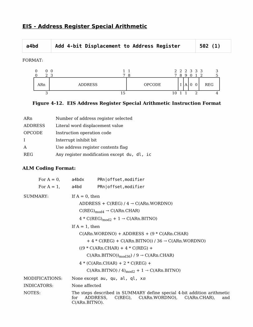
EIS - Address Register Special Arithmetic
a4bd Add 4-bit Displacement to Address Register 502 (1)
FORMAT:
Figure 4-12. EIS Address Register Special Arithmetic Instruction Format
ARn Number of address register selected
ADDRESS Literal word displacement value
OPCODE Instruction operation code
I Interrupt inhibit bit
A Use address register contents flag
REG Any register modification except du, dl, ic
ALM Coding Format:
For A = 0, a4bdx PRn|offset,modifier
For A = 1, a4bd PRn|offset,modifier
SUMMARY: If A = 0, then
ADDRESS + C(REG) / 4 C(ARn.WORDNO)→
C(REG)mod4 C(ARn.CHAR)→
4 * C(REG)mod2 + 1 C(ARn.BITNO)→
If A = 1, then
C(ARn.WORDNO) + ADDRESS + (9 * C(ARn.CHAR)
+ 4 * C(REG) + C(ARn.BITNO)) / 36 C(ARn.WORDNO)→
((9 * C(ARn.CHAR) + 4 * C(REG) +
C(ARn.BITNO))mod36) / 9 C(ARn.CHAR)→
4 * (C(ARn.CHAR) + 2 * C(REG) +
C(ARn.BITNO) / 4)mod2 + 1 C(ARn.BITNO)→
MODIFICATIONS: None except au, qu, al, ql, xn
INDICATORS: None affected
NOTES: The steps described in SUMMARY define special 4-bit addition arithmetic for ADDRESS, C(REG), C(ARn.WORDNO), C(ARn.CHAR), and C(ARn.BITNO).
00
ARn
02
3
03
17
ADDRESS
15
18
27
OPCODE
10
28
I
1
29
A
1
30
0
31
0
2
32
35
REG
4

C(REG) is always treated as a count of 4-bit characters.
The use of an address register is inherent; the value of bit 29 in the instruction word affects operand evaluation but not register selection.
Attempted repetition with the rpt, rpd, or rpl instructions causes an illegal procedure fault.
a6bd Add 6-bit Displacement to Address Register 501 (1)
FORMAT: EIS address register special arithmetic instruction format (see Figure 4-12).
ALM Coding Format:
For A = 0, a6bdx PRn|offset,modifier
For A = 1, a6bd PRn|offset,modifier
SUMMARY: If A = 0, then
ADDRESS + C(REG) / 6 C(ARn.WORDNO)→
((6 * C(REG))mod36) / 9 C(ARn.CHAR)→
(6 * C(REG))mod9 C(ARn.BITNO)→
If A = 1, then
C(ARn.WORDNO) + ADDRESS + (9 * C(ARn.CHAR) +
6 * C(REG) + C(ARn.BITNO)) / 36 C(ARn.WORDNO)→
((9 * C(ARn.CHAR) + 6 * C(REG) +
C(ARn.BITNO))mod36) / 9 C(ARn.CHAR)→
(9 * C(ARn.CHAR) + 6 * C(REG) +
C(ARn.BITNO))mod9 C(ARn.BITNO)→
MODIFICATIONS: None except au, qu, al, ql, xn
INDICATORS: None affected
NOTES: The steps described in SUMMARY define special 6-bit addition arithmetic for ADDRESS, C(REG), C(ARn.WORDNO), C(ARn.CHAR), and C(ARn.BITNO).
C(REG) is always treated as a count of 6-bit characters.
The use of an address register is inherent; the value of bit 29 in the instruction word affects address preparation but not register selection.
Attempted repetition with the rpt, rpd, or rpl instructions causes an illegal procedure fault.
a9bd Add 9-bit Displacement to Address Register 500 (1)
FORMAT: EIS address register special arithmetic instruction format (see Figure 4-12).

ALM Coding Format:
For A = 0, a9bdx PRn|offset,modifier
For A = 1, a9bd PRn|offset,modifier
SUMMARY: If A = 0, then
ADDRESS + C(REG) / 4 C(ARn.WORDNO)→
C(REG)mod4 C(ARn.CHAR)→
If A = 1, then
C(ARn.WORDNO) + ADDRESS +
(C(REG) + C(ARn.CHAR)) / 4 C(ARn.WORDNO)→
(C(ARn.CHAR) + C(REG))mod4 C(ARn.CHAR)→
0000 C(ARn.BITNO)→
MODIFICATIONS: None except au, qu, al, ql, xn
INDICATORS: None affected
NOTES: The steps described in SUMMARY define special 9-bit addition arithmetic for ADDRESS, C(REG), C(ARn.WORDNO), and C(ARn.CHAR).
C(REG) is always treated as a count of 9-bit bytes.
The use of an address register is inherent; the value of bit 29 in the instruction word affects operand evaluation but not register selection.
Attempted repetition with the rpt, rpd, or rpl instructions causes an illegal procedure fault.
abd Add Bit Displacement to Address Register 503 (1)
FORMAT: EIS address register special arithmetic instruction format (see Figure 4-12).
ALM Coding Format:
For A = 0, abdx PRn|offset,modifier
For A = 1, abd PRn|offset,modifier
SUMMARY: If A = 0, then
ADDRESS + C(REG) / 36 C(ARn.WORDNO)→
(C(REG)mod36) / 9 C(ARn.CHAR)→
C(REG)mod9 C(ARn.BITNO)→
If A = 1, then
C(ARn.WORDNO) + ADDRESS + (9 * C(ARn.CHAR)
+ 36 * C(REG) + C(ARn.BITNO)) / 36 C(ARn.WORDNO)→
((9 * C(ARn.CHAR) + 36 * C(REG) +
C(ARn.BITNO))mod36) / 9 C(ARn.CHAR)→
(9 * C(ARn.CHAR) + 36 * C(REG) +
C(ARn.BITNO))mod9 C(ARn.BITNO)→
MODIFICATIONS: None except au, qu, al, ql, xn
INDICATORS: None affected
NOTES: The steps described in SUMMARY define special bit addition arithmetic for ADDRESS, C(REG), C(ARn.WORDNO), C(ARn.CHAR), and C(ARn.BITNO).
C(REG) is always treated as a bit count.
The use of an address register is inherent; the value of bit 29 in the instruction word affects operand evaluation but not register selection.
Attempted repetition with the rpt, rpd, or rpl instructions causes an illegal procedure fault.
awd Add Word Displacement to Address Register 507 (1)
FORMAT: EIS address register special arithmetic instruction format (see Figure 4-12).
ALM Coding Format:
For A = 0, awdx PRn|offset,modifier
For A = 1, awd PRn|offset,modifier
SUMMARY: If A = 0, then
ADDRESS + C(REG) C(ARn.WORDNO)→
If A = 1, then
C(ARn.WORDNO) + ADDRESS + C(REG) C(ARn.WORDNO)→
00 C(ARn.CHAR)→
0000 C(ARn.BITNO)→
MODIFICATIONS: None except au, qu, al, ql, xn
INDICATORS: None affected
NOTES: The use of an address register is inherent; the value of bit 29 in the instruction word affects operand evaluation but not register selection.
C(REG) is always treated as a word count.
Attempted repetition with the rpt, rpd, or rpl instructions causes an illegal procedure fault.

s4bd Subtract 4-bit Displacement from Address Register
522 (1)
FORMAT: EIS address register special arithmetic instruction format (see Figure 4-12).
ALM Coding Format:
For A = 0, s4bdx PRn|offset,modifier
For A = 1, s4bd PRn|offset,modifier
SUMMARY: If A = 0, then
- (ADDRESS + C(REG) / Ah) C(ARn.WORDNO)→
- C(REG)mod4 C(ARn.CHAR)→
- 4 * C(REG)mod2 + 1 C(ARn.BITNO)→
If A = 1, then
C(ARn.WORDNO) - ADDRESS + (9 * C(ARn.CHAR)
- 4 * C(REG) + C(ARn.BITNO)) / 36 C(ARn.WORDNO)→
((9 * C(ARn.CHAR) - 4 * C(REG) +
C(ARn.BITNO))mod36) / 9 C(ARn.CHAR)→
4 * (C(ARn.CHAR) - 2 * C(REG) +
C(ARn.BITNO) / 4)mod2 + 1 C(ARn.BITNO)→
MODIFICATIONS: None except au, qu, al, ql, xn
INDICATORS: None affected
NOTES: The steps described in SUMMARY define special 4-bit subtraction arithmetic for ADDRESS, C(REG), C(ARn.WORDNO), C(ARn.CHAR), and C(ARn.BITNO).
C(REG) is always treated as a count of 4-bit characters.
The use of an address register is inherent; the value of bit 29 in the instruction word affects operand evaluation but not register selection.
Attempted repetition with the rpt, rpd, or rpl instructions causes an illegal procedure fault.
s6bd Subtract 6-bit Displacement from Address Register
521 (1)
FORMAT: EIS address register special arithmetic instruction format (see Figure 4-12).
ALM Coding Format:
For A = 0, s6bdx PRn|offset,modifier
For A = 1, s6bd PRn|offset,modifier
SUMMARY: If A = 0, then
- (ADDRESS + C(REG) / 6) C(ARn.WORDNO)→
- ((6 * C(REG))mod36) / 9 C(ARn.CHAR)→
- (6 * C(REG))mod9 C(ARn.BITNO)→
If A = 1, then
C(ARn.WORDNO) - ADDRESS + (9 * C(ARn.CHAR)
- 6 * C(REG) + C(ARn.BITNO)) / 36 C(ARn.WORDNO)→
((9 * C(ARn.CHAR) - 6 * C(REG) +
C(ARn.BITNO))mod36) / 9 C(ARn.CHAR)→
(9 * C(ARn.CHAR) - 6 * C(REG) +
C(ARn.BITNO))mod9 C(ARn.BITNO)→
MODIFICATIONS: None except au, qu, al, ql, xn
INDICATORS: None affected
NOTES: The steps described in SUMMARY define special 6-bit subtraction arithmetic for ADDRESS, C(REG), C(ARn.WORDNO), C(ARn.CHAR), and C(ARn.BITNO).
C(REG) is always treated as a count of 6-bit characters.
The use of an address register is inherent; the value of bit 29 in the instruction word affects operand evaluation but not register selection.
Attempted repetition with the rpt, rpd, or rpl instructions causes an illegal procedure fault.
s9bd Subtract 9-bit Displacement from Address Register
520 (1)
FORMAT: EIS address register special arithmetic instruction format (see Figure 4-12).
ALM Coding Format:
For A = 0, s9bdx PRn|offset,modifier
For A = 1, s9bd PRn|offset,modifier
SUMMARY: If A = 0, then
- (ADDRESS + C(REG) / 4) C(ARn.WORDNO)→
- C(REG)mod4 C(ARn.CHAR)→
If A = 1, then
C(ARn.WORDNO) - ADDRESS +
(C(ARn.CHAR) - C(REG)) / 4 C(ARn.WORDNO)→
(C(ARn.CHAR) - C(REG))mod4 C(ARn.CHAR)→
0000 C(ARn.BITNO)→
MODIFICATIONS: None except au, qu, al, qu, xn

INDICATORS: None affected
NOTES: The steps described in SUMMARY define special 9-bit subtraction arithmetic for ADDRESS, C(REG), C(ARn.WORDNO), and C(ARn.CHAR).
C(REG) is always treated as a count of 9-bit bytes.
The use of an address register is inherent: the value of bit 29 in the instruction word affects operand evaluation but not register selection.
Attempted repetition with the rpt, rpd, or rpl instructions causes an illegal procedure fault.
sbd Subtract Bit Displacement from Address Register
523 (1)
FORMAT: EIS address register special arithmetic instruction format (see Figure 4-12).
ALM Coding Format:
For A = 0, sbdx PRn|offset,modifier
For A = 1, sbd PRn|offset,modifier
SUMMARY: If A = 0, then
- (ADDRESS + C(REG) / 36) C(ARn.WORDNO)→
- (C(REG)mod36) / 9 C(ARn.CHAR)→
- C(REG)mod9 C(ARn.BITNO)→
If A = 1, then
C(ARn.WORDNO) - ADDRESS + (9 * C(ARn.CHAR)
- 36 * C(REG) + C(ARn.BITNO)) / 36 C(ARn.WORDNO)→
((9 * C(ARn.CHAR) - 36 * C(REG) +
C(ARn.BITNO))mod36) / 9 C(ARn.CHAR)→
(9 * C(ARn.CHAR) - 36 * C(REG) +
C(ARn.BITNO))mod9 C(ARn.BITNO)→
MODIFICATIONS: None except au, qu, al, ql, xn
INDICATORS: None affected
NOTES: The steps described in SUMMARY define special bit subtraction arithmetic for ADDRESS, C(REG), C(ARn.WORDNO), C(ARn.CHAR), and C(ARn.BITNO).
C(REG) is always treated as a bit count.
The use of an address register is inherent; the value of bit 29 in the instruction word affects operand evaluation but not register selection.
Attempted repetition with the rpt, rpd, or rpl instructions causes an illegal procedure fault.

swd Subtract Word Displacement from Address Register
527 (1)
FORMAT: EIS address register special arithmetic instruction format (see Figure 4-12).
ALM Coding Format:
For A = 0, swdx PRn|offset,modifier
For A = 1, swd PRn|offset,modifier
SUMMARY: If A = 0, then
- (ADDRESS + C(REG)) C(ARn.WORDNO)→
If A = 1, then
C(ARn.WORDNO) - (ADDRESS + C(REG)) C(ARn.WORDNO)→
00 C(ARn.CHAR)→
0000 C(ARn.BITNO)→
MODIFICATIONS: None except au, qu, al, ql, xn
INDICATORS: None affected
NOTES: The use of an address register is inherent; the value of bit 29 in the instruction word affects operand evaluation but not register selection.
Attempted repetition with the rpt, rpd, or rpl instructions causes an illegal procedure fault.
EIS - Alphanumeric Compare
cmpc Compare Alphanumeric Character Strings 106 (1)
FORMAT:
Figure 4-13. Compare Alphanumeric Character Strings (cmpc)EIS Multiword Instruction Format
FILL Fill character for string extension
MF1 Modification field for operand descriptor 1
MF2 Modification field for operand descriptor 2
I Interrupt inhibit bit
Y-charn1 Address of left-hand string
CN1 First character position of left-hand string
TA1 Data type of left-hand string
N1 Length of left-hand string
Y-charn2 Address of right-hand string
CN2 First character position of right-hand string
N2 Length of right-hand string
ALM Coding Format:
cmpc (MF1),(MF2)[,fill(octalexpression)]
descna Y-charn1[(CN1)],N1 n = 4, 6, or 9 (TA1 = 2, 1, or 0)
descna Y-charn2[(CN2)],N2 n = 4, 6, or 9 (TA2 is ignored)
SUMMARY: For i = 1, 2, ..., minimum (N1,N2)
C(Y-charn1)i-1 :: C(Y-charn2)i-1
If N1 < N2, then for i = N1+1, N1+2, ..., N2
C(FILL) :: C(Y-charn2)i-1
00
08
09
10
11
17
18
20
21
22
23
24
27
28
29
35
FILL
9
0 0
2
MF2
7
106 (1)
10
I
1
MF1
7Y-charn1 CN1 TA1
2
0
1
N1
CN2
3
0 0 0
3
N2
1218
Y-charn2

If N1 > N2, then for i = N2+1, N2+2, ..., N1
C(Y-charn1)i-1 :: C(FILL)
MODIFICATIONS: None except au, qu, al, ql, xn for MF1 and MF2
INDICATORS: (Indicators not listed are not affected)
Zero If C(Y-charn1)i-1 = C(Y-charn2)i-1 for all i, then ON; otherwise, OFF
Carry If C(Y-charn1)i-1 < C(Y-charn2)i-1 for any i, then OFF; otherwise ON
NOTES: Both strings are treated as the data type given for the left-hand string, TA1. A data type given for the right-hand string, TA2, is ignored.
Comparison is made on full 9-bit fields. If the given data type is not 9-bit (TA1 ≠ 0), then characters from C(Y-charn1) and C(Y-charn2) are high-order zero filled. All 9 bits of C(FILL) are used.
Instruction execution proceeds until an inequality is found or the larger string length count is exhausted.
If MFk.RL = 1, then Nk does not contain the operand length; instead, it contains a register code for a register holding the operand length.
If MFk.ID = 1, then the kth word following the instruction word does not contain an operand descriptor; instead, it contains an indirect pointer to the operand descriptor.
Attempted execution with the xed instruction causes an illegal procedure fault.
Attempted repetition with the rpt, rpd, or rpl instructions causes an illegal procedure fault.
scd Scan Characters Double 120 (1)
FORMAT:
Figure 4-14. Scan Characters Double (scd) EIS Multiword Instruction Format
MF1 Modification field for operand descriptor 1
MF2 Modification field for operand descriptor 2
I Interrupt inhibit bit
Y-charn1 Address of string
30
31
32
00
10
11
17
18
20
21
22
23
24
27
28
29
35
0 0 0 0 0 0 0 0 0 0 0
11
MF2
7
120 (1)
10
I
1
MF1
7Y-charn1 CN1 TA1
2
0
1
N1
12CN2
3
0 0 0 0 0 0 0 0 0 0 0 0 0 0 0
15
18
0 0 0 0 0 0 0 0 0 0 0
11
A
1
0 0
2
REG
4
Y-charn2
Y3

CN1 First character position of string
TA1 Data type of string
N1 Length of string
Y-charn2 Address of test character pair
CN2 First character position of test character pair
Y3 Address of compare count word
A Indirect via pointer register flag for Y3
REG Register modifier for Y3
ALM Coding Format:
scd (MF1),(MF2)
descna Y-charn1[(CN1)],N1 n = 4, 6, or 9 (TA1 = 2, 1, or 0)
descna Y-charn2[(CN2)] n = 4, 6, or 9 (TA2 is ignored)
arg Y3[,tag]
SUMMARY: For i = 1, 2, ..., N1-1
C(Y-charn1)i-1,i :: C(Y-charn2)0,1
On instruction completion, if a match was found:
00...0 C(Y3)→ 0,11
i-1 C(Y3)→ 12,35
If no match was found:
00...0 C(Y3)→ 0,11
N1-1 C(Y3)→ 12,35
MODIFICATIONS: None except au, qu, al, ql, xn for MF1 and REG
None except du, au, qu, al, ql, xn for MF2
INDICATORS: (Indicators not listed are not affected)
Tally runout If the string length count is exhausted without a match, or if N1 = 1, then ON; otherwise OFF
NOTES: Both the string and the test character pair are treated as the data type given for the string, TA1. A data type given for the test character pair, TA2, is ignored.
Instruction execution proceeds until a character pair match is found or the string length count is exhausted.
If MFk.RL = 1, then Nk does not contain the operand length; instead, it contains a register code for a register holding the operand length.
If MFk.ID = 1, then the kth word following the instruction word does not contain an operand descriptor; instead, it contains an indirect pointer to the operand descriptor.
If MF2.ID = 0 and MF2.REG = du, then the second word following the instruction word does not contain an operand descriptor for the test character pair; instead, it contains the test character pair as a direct upper operand in bits 0,17.
Attempted execution with the xed instruction causes an illegal procedure fault.

Attempted repetition with the rpt, rpd, or rpl instructions causes an illegal procedure fault.
scdr Scan Characters Double in Reverse 121 (1)
FORMAT: Same as Scan Characters Double (scd) format (see Figure 4-14).
SUMMARY: For i = 1, 2, ..., N1-1
C(Y-charn1)N1-i-1,N1-i :: C(Y-charn2)0,1
On instruction completion, if a match was found:
00...0 C(Y3)→ 0,11
i-1 C(Y3)→ 12,35
If no match was found:
00...0 C(Y3)→ 0,11
N1-1 C(Y3)→ 12,35
MODIFICATIONS: None except au, qu, al, ql, xn for MF1 and REG
None except du, au, qu, al, ql, xn for MF2
INDICATORS: (Indicators not listed are not affected)
Tally runout If the string length count is exhausted without a match, or if N1 = 1, then ON; otherwise OFF
NOTES: Both the string and the test character pair are treated as the data type given for the string, TA1. A data type given for the test character pair, TA2, is ignored.
Instruction execution proceeds until a character pair match is found or the string length count is exhausted.
If MFk.RL = 1, then Nk does not contain the operand length; instead, it contains a register code for a register holding the operand length.
If MFk.ID = 1, then the kth word following the instruction word does not contain an operand descriptor; instead, it contains an indirect pointer to the operand descriptor .
If MF2.ID = 0 and MF2.REG = du, then the second word following the instruction word does not contain an operand descriptor for the test character pair; instead, it contains the test character pair as a direct upper operand in bits 0, 17.
Attempted execution with the xed instruction causes an illegal procedure fault.
Attempted repetition with the rpt, rpd, or rpl instructions causes an illegal procedure fault.

scm Scan with Mask 124 (1)
FORMAT:
Figure 4-15. Scan with Mask (scm) EIS Multiword Instruction Format
MASK Comparison bit mask
MF1 Modification field for operand descriptor 1
MF2 Modification field for operand descriptor 2
I Interrupt inhibit bit
Y-charn1 Address of string
CN1 First character position of string
TA1 Data type of string
N1 Length of string
Y- charn2 Address of test character
CN2 First character position of test character
Y3 Address of compare count word
A Indirect via pointer register flag for Y3
REG Register modifier for Y3
ALM Coding Format:
scm (MF1),(MF2)[,mask(octalexpression)]
descna Y-charn1[(CN1)],N1 n = 4, 6, or 9 (TA1 = 2, 1, or 0)
descna Y-charn2[(CN2)] n = 4, 6, or 9 (TA2 is ignored)
arg Y3[,tag]
SUMMARY: For characters i = 1, 2, ..., N1
For bits j = 0, 1, ..., 8
C(Z)j = ~C(MASK)j & ((C(Y-charn1)i-1 )j (C(Y-char⊕ n2)0)j)
00
08
09
10
11
17
18
20
21
22
23
24
27
28
29
35
MASK
9
0 0
2
MF2
7
124 (1)
10
I
1
MF1
7Y-charn1 CN1 TA1
2
0
1
N1
12CN2
3
0 0 0 0 0 0 0 0 0 0 0 0 0 0 0
15
18
0 0 0 0 0 0 0 0 0 0 0
11
A
1
0 0
2
REG
4
Y-charn2
Y3
30
31
32
If C(Z)0,8 = 00...0, then
00...0 C(Y3)→ 0,11
i-1 C(Y3)→ 12,35
otherwise, continue scan of C(Y-charn1)
If a masked character match was not found, then
00...0 C(Y3)→ 0,11
N1 C(Y3)→ 12,35
MODIFICATIONS: None except au, qu, al, ql, xn for MF1 and REG
None except du, au, qu, al, ql, xn for MF2
INDICATORS: (Indicators not listed are not affected)
Tally runout If the string length count exhausts, then ON; otherwise, OFF
NOTES: Both the string and the test character pair are treated as the data type given for the string, TA1. A data type given for the test character pair, TA2, is ignored.
1 bits in C(MASK) specify those bits of each character that will not take part in the masked comparison.
Instruction execution proceeds until a masked character match is found or the string length count is exhausted.
Masking and comparison is done on full 9-bit fields. If the given data type is not 9-bit (TA1 ≠ 0), then characters from C(Y-charn1) and C(Y-charn2) are high-order zero filled. All 9 bits of C(MASK) are used.
If MF1.RL = 1, then N1 does not contain the operand length; instead, it contains a register code for a register holding the operand length.
If MFk.ID = 1, then the kth word following the instruction word does not contain an operand descriptor; instead, it contains an indirect pointer to the operand descriptor.
If MF2.ID = 0 and MF2.REG = du, then the second word following the instruction word does not contain an operand descriptor for the test character; instead, it contains the test character as a direct upper operand in bits 0,8.
Attempted execution with the xed instruction causes an illegal procedure fault.
Attempted repetition with the rpt, rpd, or rpl instructions causes an illegal procedure fault.
scmr Scan with Mask in Reverse 125 (1)
FORMAT: Same as Scan with Mask (scm) format (see Figure 4-15).
SUMMARY: For characters i = 1, 2, ..., N1
For bits j = 0, 1, ..., 8
C(Z)j = ~C(MASK)j & ((C(Y-charn1)N1-i)j (C(Y-char⊕ n2)0)j)

If C(Z)0,8 = 00...0, then
00...0 C(Y3)→ 0,11
i-1 C(Y3)→ 12,35
otherwise, continue scan of C(Y-charn1)
If a masked character match was not found, then
00...0 C(Y3)→ 0,11
N1 C(Y3)→ 12,35
MODIFICATIONS: None except au, qu, al, ql, xn for MF1 and REG
None except du, au, qu, al, ql, xn for MF2
INDICATORS: (Indicators not listed are not affected)
Tally runout If the string length count exhausts, then ON; otherwise, OFF
NOTES: Both the string and the test character are treated as the data type given for the string, TA1. A data type given for the test character, TA2, is ignored.
1 bits in C(MASK) specify those bits of each character that will not take part in the masked comparison.
Instruction execution proceeds until a masked character match is found or the string length count is exhausted.
Masking and comparison is done on full 9-bit fields. If the given data type is not 9-bit (TA1 ≠ 0), then characters from C(Y-charn1) and C(Y-charn2) are high-order zero filled. All 9 bits of C(MASK) are used.
If MF1.RL = 1, then N1 does not contain the operand length; instead, it contains a register code for a register holding the operand length.
If MFk.ID = 1, then the kth word following the instruction word does not contain an operand descriptor; instead, it contains an indirect pointer to the operand descriptor.
If MF2.ID = 0 and MF2.REG = du, then the second word following the instruction word does not contain an operand descriptor for the test character; instead, it contains the test character as a direct upper operand in bits 0,8.
Attempted execution with the xed instruction causes an illegal procedure fault.
Attempted repetition with the rpt, rpd, or rpl instructions causes an illegal procedure fault.
tct Test Character and Translate 164 (1)
FORMAT:
Figure 4-16. Test Character and Translate (tct)EIS Multiword Instruction Format
MF1 Modification field for operand descriptor 1
I Interrupt inhibit bit
Y-charn1 Address of string
CN1 First character position of string
TA1 Data type of string
N1 Length of string
Y-char92 Address of character translation table
Y3 Address of result word
A Indirect via pointer register flag for Y2 and Y3
REG Register modifier for Y2 and Y3
ALM Coding Format:
tct (MF1)
descna Y-charn1[(CN1)],N1 n = 4, 6, or 9 (TA1 = 2, 1, or 0)
arg Y-char92[,tag]
arg Y3[,tag]
SUMMARY: For i = 1, 2, ..., N1
m = C(Y-charn1)i-1
If C(Y-char92)m ≠ 00...0, then
C(Y-char92)m C(Y3)→ 0,8
000 C(Y3)→ 9,11
i-1 C(Y3)→ 12,35
otherwise, continue scan of C(Y-charn1)
00
17
18
20
21
22
23
24
27
28
29
35
0 0 0 0 0 0 0 0 0 0 0 0 0 0 0 0 0 0 164 (1)
10
I
1
MF1
7Y-charn1 CN1
3
TA1
2
0
1
N1
120 0 0 0 0 0 0 0 0 0 0 A 0 0 REG
18
0 0 0 0 0 0 0 0 0 0 0
11
A
1
0 0
2
REG
4
Y-char92
Y3
30
31
32
If a non-zero table entry was not found, then
00...0 C(Y3)→ 0,11
N1 C(Y3)→ 12,3
MODIFICATIONS: None except au, qu, al, ql, xn for MF1 and MF2
INDICATORS: (Indicators not listed are not affected)
Tally runout If the string length count exhausts, then ON; otherwise, OFF
NOTES: If the data type of the string to be scanned is not 9-bit (TA1 ≠ 0), then characters from C(Y-charn1) are high-order zero filled in forming the table index, m.
Instruction execution proceeds until a non-zero table entry is found or the string length count is exhausted.
If MF1.RL = 1, then N1 does not contain the operand length; instead, it contains a register code for a register holding the operand length.
If MF1.ID = 1, then the first word following the instruction word does not contain an operand descriptor; instead, it contains an indirect pointer to the operand descriptor.
Attempted execution with the xed instruction causes an illegal procedure fault.
Attempted repetition with the rpt, rpd, or rpl instructions causes an illegal procedure fault.
The character number of Y-char92 must be zero, i.e., Y-char92 must start on a word boundary.
If a non-zero table entry was not found, then
00...0 C(Y3)→ 0,11
N1 C(Y3)→ 12,35
tctr Test Character and Translate in Reverse 165 (1)
FORMAT: Same as Test Character and Translate (tct) format (see Figure 4-16).
SUMMARY: For i = 1, 2, ..., N1
m = C(Y-charn1)N1-i
If C(Y-char92)m ≠ 00...0, then
C(Y-char92)m C(Y3)→ 0,8
000 C(Y3)→ 9,11
i-1 C(Y3)→ 12,35
otherwise, continue scan of C(Y-charn1)
If a non-zero table entry was not found, then
00...0 C(Y3)→ 0,11
N1 C(Y3)→ 12,35
MODIFICATIONS: None except au, qu, al, ql, xn for MF1 and REG
INDICATORS: (Indicators not listed are not affected)
Tally runout If the string length count exhausts, then ON; otherwise, OFF

NOTES: If the data type of the string to be scanned is not 9-bit (TA1 ≠ 0), then characters from C(Y-charn1) are high-order zero filled in forming the table index, m.
Instruction execution proceeds until a non-zero table entry is found or the string length count is exhausted.
If MF1.RL = 1, then N1 does not contain the operand length; instead, it contains a register code for a register holding the operand length.
If MF1.ID = 1, then the first word following the instruction word does not contain an operand descriptor; instead, it contains an indirect pointer to the operand descriptor.
Attempted execution with the xed instruction causes an illegal procedure fault.
Attempted repetition with the rpt, rpd, or rpl instructions causes an illegal procedure fault.

EIS - Alphanumeric Move
mlr Move Alphanumeric Left to Right 100 (1)
FORMAT:
Figure 4-17. Move Alphanumeric Left to Right (mlr)EIS Multiword Instruction Format
FILL Fill character for string extension
T Truncation fault enable bit
MF1 Modification field for operand descriptor 1
MF2 Modification field for operand descriptor 2
Y-charn1 Address of sending string
CN1 First character position of sending string
TA1 Data type of sending string
N1 Length of sending string
Y- charn2 Address of receiving string
CN2 First character position of receiving string
TA2 Data type of receiving string
N2 Length of receiving string
ALM Coding Format:
mlr (MF1),(MF2)[,fill(octalexpression)][,enablefault]
descna Y-charn1[(CN1)],N1 n = 4, 6, or 9 (TA1 = 2, 1, or 0)
descna Y-charn2[(CN2)],N2 n = 4, 6, or 9 (TA2 = 2, 1, or 0)
SUMMARY: For i = 1, 2, ..., minimum (N1,N2)
C(Y-charn1)i-1 C(Y-char→ n2)i-1
If N1 < N2, then for i = N1+1, N1+2, ..., N2
C(FILL) C(Y-char→ n2)i-1
00
08
09
10
11
17
18
20
21
22
23
24
27
28
29
35
FILL
9
T 0 MF2
7
100 (1)
10
I
1
MF1
7Y-charn1 CN1 TA1
2
0 N1
CN2
3
TA2 0
1
N2
1218
Y-charn2
1 1
MODIFICATIONS: None except au, qu, al, ql, xn for MF1 and MF2
INDICATORS: (Indicators not listed are not affected)
Truncation If N1 > N2 then ON; otherwise OFF
NOTES: If data types are dissimilar (TA1 ≠ TA2), each character is high-order truncated or zero filled, as appropriate, as it is moved. No character conversion takes place.
If N1 > N2, then (N1-N2) trailing characters of C(Y-charn1) are not moved and the truncation indicator is set ON.
If N1 < N2 and TA2, = 2 (4-bit data) or 1 (6-bit data), then FILL characters are high-order truncated as they are moved to C(Y-charn2). No character conversion takes place.
If N1 < N2, C(FILL)0 = 1, TA1 = 1, and TA2 = 2, then C(Y-charn1)N1-1 is examined for a GBCD overpunch sign. If a negative overpunch sign is found, then the minus sign character is placed in C(Y-charn2)N2-1; otherwise, a plus sign character is placed in C(Y-charn2)N2-1.
If MFk.RL = 1,, then Nk does not contain the operand length; instead, it contains a register code for a register holding the operand length.
If MFk.ID = 1, then the kth word following the instruction word does not contain an operand descriptor; instead, it contains an indirect pointer to the operand descriptor.
C(Y-charn1) and C(Y-charn2) may be overlapping strings; no check is made. This feature is useful for replication of substrings within a larger string, but care must be exercised in the construction of the operand descriptors so that sending string, C(Y-charn1), data is not inadvertently destroyed.
The user of string replication or overlaying is warned that the decimal unit addresses the main memory in unaligned (not on modulo 8 boundary) units of Y-block8 words and that the overlayed string, C(Y-charn2), is not returned to main memory until the unit of Y-block8 words is filled or the instruction completes.
If T = 1 and the truncation indicator is set ON by execution of the instruction, then a truncation (overflow) fault occurs.
Attempted execution with the xed instruction causes an illegal procedure fault.
Attempted repetition with the rpt, rpd, or rpl instructions causes an illegal procedure fault.
mrl Move Alphanumeric Right to Left 101 (1)
FORMAT: Same as Move Alphanumeric Left to Right (mlr) format (see Figure 4-17).
SUMMARY: For i = 1, 2, ..., minimum (N1,N2)
C(Y-charn1)N1-i C(Y-char→ n2)N2-i
If N1 < N2, then for i = N1+1, N1+2, ..., N2
C(FILL) C(Y-char→ n2)N2-i
MODIFICATIONS: None except au, qu, al, ql, xn for MF1 and MF2
INDICATORS: (Indicators not list,ed are not affected)
Truncation If N1 > N2 then ON; otherwise OFF
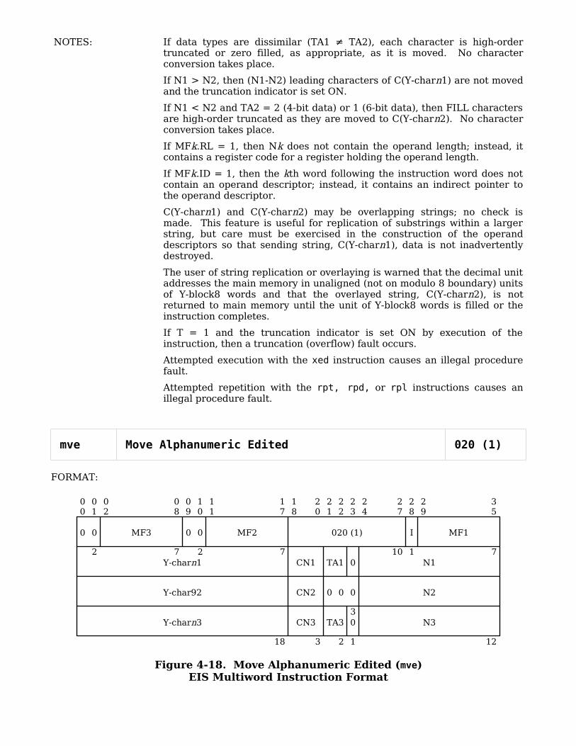
NOTES: If data types are dissimilar (TA1 ≠ TA2), each character is high-order truncated or zero filled, as appropriate, as it is moved. No character conversion takes place.
If N1 > N2, then (N1-N2) leading characters of C(Y-charn1) are not moved and the truncation indicator is set ON.
If N1 < N2 and TA2 = 2 (4-bit data) or 1 (6-bit data), then FILL characters are high-order truncated as they are moved to C(Y-charn2). No character conversion takes place.
If MFk.RL = 1, then Nk does not contain the operand length; instead, it contains a register code for a register holding the operand length.
If MFk.ID = 1, then the kth word following the instruction word does not contain an operand descriptor; instead, it contains an indirect pointer to the operand descriptor.
C(Y-charn1) and C(Y-charn2) may be overlapping strings; no check is made. This feature is useful for replication of substrings within a larger string, but care must be exercised in the construction of the operand descriptors so that sending string, C(Y-charn1), data is not inadvertently destroyed.
The user of string replication or overlaying is warned that the decimal unit addresses the main memory in unaligned (not on modulo 8 boundary) units of Y-block8 words and that the overlayed string, C(Y-charn2), is not returned to main memory until the unit of Y-block8 words is filled or the instruction completes.
If T = 1 and the truncation indicator is set ON by execution of the instruction, then a truncation (overflow) fault occurs.
Attempted execution with the xed instruction causes an illegal procedure fault.
Attempted repetition with the rpt, rpd, or rpl instructions causes an illegal procedure fault.
mve Move Alphanumeric Edited 020 (1)
FORMAT:
Figure 4-18. Move Alphanumeric Edited (mve)EIS Multiword Instruction Format
00
01
02
08
09
10
11
17
18
20
21
22
23
24
27
28
29
35
0 0
2
MF3
7
0 0
2
MF2
7
020 (1)
10
I
1
MF1
7Y-charn1 CN1 TA1 0 N1
CN2 0 0 0 N2
18
CN3
3
TA3
2
0
1
N3
12
Y-char92
Y-charn33

MF1 Modification field for operand descriptor 1
MF2 Modification field for operand descriptor 2
MF3 Modification field for operand descriptor 3
I Interrupt inhibit bit
Y-charn1 Address of sending string
CN1 First character position of sending string
TA1 Data type of sending string
N1 Length of sending string
Y-char92 Address of MOP control string
CN2 First character position of MOP control string
N2 Length of MOP control string
Y-charn3 Address of receiving string
CN3 First character position of receiving string
TA3 Data type of receiving string
N3 Length of receiving string
ALM Coding Format:
mve (MF1),(MF2),(MF3)
descna Y-charn1[(CN1)],N1 n = 4, 6, or 9 (TA1 = 2, 1, or 0)
desc9a Y-char92[(CN2)],N2
descna Y-charn3[(CN3)],N3 n = 4, 6, or 9 (TA3 = 2, 1, or 0)
SUMMARY: C(Y-charn1) C(Y-char→ n3) under C(Y-char92) MOP control
See "Micro Operations for Edit Instructions" later in this section for details of editing under MOP control.
MODIFICATIONS: None except au, qu, al, ql, xn for MF1, MF2, and MF3
INDICATORS: None affected
NOTES: If data types are dissimilar (TA1 ≠ TA3), each character of C(Y-charn1) is high-order truncated or zero filled, as appropriate, as it is moved. No character conversion takes place.
If the data type of the receiving string is not 9-bit (TA3 = 0), then insertion characters are high-order truncated as they are inserted.
The maximum string length is 63. The count fields N1, N2, and N3 are treated as modulo 64 numbers.
The instruction completes normally only if N3 is the first tally to exhaust: otherwise, an illegal procedure fault occurs.
If MFk.RL = 1, then Nk does not contain the operand length; instead, it contains a register code for a register holding the operand length.
If MFk.ID = 1, then the kth word following the instruction word does not contain an operand descriptor; instead, it contains an indirect pointer to the operand descriptor.

C(Y-charn1) and C(Y-charn3) may be overlapping strings; no check is made. This feature is useful for replication of substrings within a larger string, but care must be exercised in the construction of the operand descriptors so that sending string, C(Y-charn1), data is not inadvertently destroyed.
The user of string replication or overlaying is warned that the decimal unit addresses the main memory in unaligned (not on modulo 8 boundary) units of Y-block8 words and that the overlayed string, C(Y-charn3), is not returned to main memory until the unit of Y-block8 words is filled or the instruction completes.
Attempted execution with the xed instruction causes an illegal procedure fault.
Attempted repetition with the rpt, rpd, or rpl instructions causes an illegal procedure fault.
mvt Move Alphanumeric with Translation 160 (1)
FORMAT:
Figure 4-19. Move Alphanumeric with Translation (mvt)EIS Multiword Instruction Format
FILL Fill character for string extension
T Truncation fault enable bit
MF1 Modification field for operand descriptor 1
MF2 Modification field for operand descriptor 2
Y-charn1 Address of sending string
CN1 First character position of sending string
TA1 Data type of sending string
N1 Length of sending string
Y- charn2 Address of receiving string
CN2 First character position of receiving string
TA2 Data type of receiving string
N2 Length of receiving string
00
01
02
08
09
10
11
17
18
20
21
22
23
24
27
28
29
35
0 0
2
MF3
7
0 0
2
MF2
7
020 (1)
10
I
1
MF1
7Y-charn1 CN1 TA1 0 N1
CN2 0 0 0 N2
18
CN3
3
TA3
2
0
1
N3
12
Y-char92
Y-charn33

Y-char93 Address of character translation table
A Indirect via pointer register flag for Y-char93
REG Register modifier for Y-char93
ALM Coding Format:
mvt (MF1),(MF2)[,fill(octalexpression)][,enablefault]
descna Y-charn1[(CN1)],N1 n = 4, 6, or 9 (TA1 = 2, 1, or 0)
descna Y-charn2[(CN2)],N2 n = 4, 6, or 9 (TA1 = 2, 1, or 0)
arg Y-char93[,tag]
SUMMARY: For i = 1, 2, ..., minimum (N1,N2)
m = C(Y-charn1)i-1
C(Y-char93)m C(Y-char→ n2)i-1
If N1 < N2, then for i = N1+1, N1+2, ..., N2
m = C(FILL)
C(Y-char93)m C(Y-char→ n2)i-1
MODIFICATIONS: None except au, qu, al, ql, xn for MF1, MF2, and REG
INDICATORS: (Indicators not listed are not affected)
Truncation If N1 > N2 then ON; otherwise OFF
NOTES: If the data type of the receiving field is not 9-bit (TA2 ≠ 0), then characters from C(Y-char93) are high-order truncated, as appropriate, as they are moved.
If the data type of the sending field is not 9-bit (TA1 ≠ 0), then characters from C(Y-charn1) are high-order zero filled when forming the table index.
If N1 > N2, then (N1-N2) trailing characters of C(Y-charn1) are not moved and the truncation indicator is set ON.
If MFk.RL = 1, then Nk does not contain the operand length; instead, it contains a register code for a register holding the operand length.
If MFk.ID = 1, then the kth word following the instruction word does not contain an operand descriptor; instead, it contains an indirect pointer to the operand descriptor.
C(Y-charn1) and C(Y-charn2) may be overlapping strings; no check is made. This feature is useful for replication of substrings within a larger string, but care must be exercised in the construction of the operand descriptors so that sending string, C(Y-charn1), data is not inadvertently destroyed.
The user of string replication or overlaying is warned that the decimal unit addresses the main memory in unaligned (not on modulo 8 boundary) units of Y-block8 words and that the overlayed string, C(Y-charn2), is not returned to main memory until the unit of Y-block8 words is filled or the instruction completes.
If T = 1 and the truncation indicator is set ON by execution of the instruction, then a truncation (overflow) fault occurs.
Attempted execution with the xed instruction causes an illegal procedure fault.
Attempted repetition with the rpt, rpd, or rpl instructions causes an illegal procedure fault.

EIS - Numeric Compare
cmpn Compare Numeric 303 (1)
FORMAT:
Figure 4-20. Compare Numeric (cmpn) EIS Multiword Instruction Format
key
MF1 Modification field for operand descriptor 1
MF2 Modification field for operand descriptor 2
I Interrupt inhibit bit
Y-charn1 Address of left-hand number
CN1 First character position of left-hand number
a TN1 Data type of left-hand number
S1 Sign and decimal type of left-hand number
SF1 Scaling factor of left-hand number
N1 Length of left-hand number
Y- charn2 Address of right-hand number
CN2 First character position of right-hand number
b TN2 Data type of right-hand number
S2 Sign and decimal type of right-hand number
SF2 Scaling factor of right-hand number
N2 Length of right-hand string
ALM Coding Format:
cmpn (MF1),(MF2)
descn[fl,ls,ns,ts] Y-charn1[(CN1)],N1,SF1 n = 4 or 9
descn[fl,ls,ns,ts] Y-charn2[(CN2)],N2,SF2 n = 4 or 9
SUMMARY: C(Y-charn1) :: C(Y-charn2) as numeric values
00
10
11
17
18
20
21
22
23
24
27
28
29
35
0 0 0 0 0 0 0 0 0 0 0
11
MF2
7
303 (1)
10
I
1
MF1
7Y-charn1 CN1 a S1 SF1
1
N1
1CN2
3
b
1
S2
2
SF2
6
N2
618
Y-charn2
30

MODIFICATIONS: None except au, qu, al, ql, xn for MF1 and MF2
INDICATORS: (Indicators not listed are not affected)
Zero If C(Y-charn1) = C(Y-charn2), then ON; otherwise OFF
Negative If C(Y-charn1) > C(Y-charn2), then ON; otherwise OFF
Carry If | C(Y-charn1) | > | C(Y-charn2) | , then OFF, otherwise ON
NOTES: Comparison is made on 4-bit numeric values contained in each character of C(Y-charnk). If either given data type is 9-bit (TNk = 0), characters from C(Y-char9k) are high-order truncated to 4 bits before comparison.
Sign characters are located according to information in CNk, Sk, and Nk and interpreted as 4-bit fields; 9-bit sign characters are high-order truncated before interpretation. The sign character 158 is interpreted as a minus sign; all other legal sign characters are interpreted as plus signs.
The position of the decimal point in C(Y-charnk) is determined from information in CNk, Sk, SFk, and Nk.
Comparison begins at the decimal position corresponding to the first digit of the operand with the larger number of integer digits and ends with the last digit of the operand with the larger number of fraction digits.
Four-bit numeric zeros are used to represent digits to the left of the first given digit of the operand with the smaller number of integer digits.
Four-bit numeric zeros are used to represent digits to the right of the last given digit of the operand with the smaller number of fraction digits.
Instruction execution proceeds until an inequality is found or the larger string length count is exhausted.
If MFk.RL = 1, then Nk does not contain the operand length; instead, it contains a register code for a register holding the operand length.
If MFk.ID = 1, then the kth word following the instruction word does not contain an operand descriptor; instead, it contains an indirect pointer to the operand descriptor.
Detection of a character outside the range [0,11]8 in a digit position or a character outside the range [12,l7]8 in a sign position causes an illegal procedure fault.
Attempted execution with the xed instruction causes an illegal procedure fault.
Attempted repetition with the rpt, rpd, or rpl instructions causes an illegal procedure fault.

EIS - Numeric Move
mvn Move Numeric 300 (1)
FORMAT:
Figure 4-21. Move Numeric (mvn) EIS Multiword Instruction Format
key
P 4-bit data sign character control
T Truncation fault enable bit
R Rounding flag
MF1 Modification field for operand descriptor 1
MF2 Modification field for operand descriptor 2
I Interrupt inhibit bit
Y-charn1 Address of sending number
CN1 First character position of sending number
a TN1 Data type of sending number
S1 Sign and decimal type of sending number
SF1 Scaling factor of sending number
N1 Length of sending number
Y- charn2 Address of receiving number
CN2 First character position of receiving number
b TN2 Data type of receiving number
S2 Sign and decimal type of receiving number
SF2 Scaling factor of receiving number
N2 Length of receiving string
00
01
08
09
10
11
17
18
20
21
22
23
24
27
28
29
35
P
1
0 0 0 0 0 0 0 0
8
T
1
R
1
MF2
7
300 (1)
10
I
1
MF1
7Y-charn1 CN1 a S1 SF1
1
N1
1CN2
3
b
1
S2
2
SF2
6
N2
618
Y-charn2
30
ALM Coding Format:
mvn (MF1),(MF2)[,enablefault][,round]
descn[fl,ls,ns,ts] Y-charn1[(CN1)],N1,SF1 n = 4 or 9
descn[fl,ls,ns,ts] Y-charn2[(CN2)],N2,SF2 n = 4 or 9
SUMMARY: C(Y-charn1) converted and/or rescaled C(Y-char→ n2)
MODIFICATIONS: None except au, qu, al, ql, xn for MF1 and MF2
INDICATORS: (Indicators not listed are not affected)
Zero If C(Y-charn2) = decimal 0, then ON; otherwise OFF
Negative If a minus sign character is moved to C(Y-charn2), then ON; otherwise OFF
Truncation If low-order digit truncation occurs without rounding, then ON; otherwise OFF
Overflow If fixed-point integer overflow occurs, then ON; otherwise unchanged. (see NOTES)
Exponent overflow
If exponent of floating-point result exceeds +127, then ON; otherwise unchanged.
Exponent underflow
If exponent of floating-point result is less than -128 then ON; otherwise unchanged.
NOTES: If data types are dissimilar (TN1 ≠ TN2), each character is high-order truncated or filled, as appropriate, as it is moved. The fill data used is "00011"b for digit characters and "00010"b for sign characters.
If TN2 and S2 specify a 4-bit signed number and P = 1, then a legal plus sign character in C(Y-charn1) is converted to 138 as it is moved.
If N2 is not large enough to hold the integer part of C(Y-charn1) as rescaled by SF2, an overflow condition exists; the overflow indicator is set ON and an overflow fault occurs. This implies that an unsigned fixed-point receiving field has a minimum length of 1 character; a signed fixed-point field, 2 characters; and a floating-point field, 3 characters.
If N2 is not large enough to hold all the given digits of C(Y-charn1) as rescaled by SF2 and R = 0, then a truncation condition exists; data movement stops when C(Y-charn2) is filled and the truncation indicator is set ON. If R = 1, then the last digit moved is rounded according to the absolute value of the remaining digits of C(Y-charn1) and the instruction completes normally.
If MFk.RL = 1, then Nk does not contain the operand length; instead, it contains a register code for a register holding the operand length.
If MFk.ID = 1, then the kth word following the instruction word does not contain an operand descriptor; instead, it contains an indirect pointer to the operand descriptor.
C(Y-charn1) and C(Y-charn2) may be overlapping strings; no check is made. This feature is useful for replication of substrings within a larger string, but care must be exercised in the construction of the operand descriptors so that sending string, C(Y-charn1), data is not inadvertently destroyed. Difficulties may be encountered because of scaling factors and the special treatment of sign characters and floating-point exponents.
The user of string replication or overlaying is warned that the decimal unit addresses the main memory in unaligned (not on modulo 8 boundary) units of Y-block8 words and that the overlayed string, C(Y-charn2), is not returned to main memory until the unit of Y-block8 words is filled or the instruction completes.

If T = 1 and the truncation indicator is set ON by execution of the instruction, then a truncation (overflow) fault occurs.
Detection of a character outside the range [0,11]8 in a digit position or a character outside the range [12,l7]8 in a sign position causes an illegal procedure fault.
Attempted execution with the xed instruction causes an illegal procedure fault.
Attempted repetition with the rpt, rpd, or rpl instructions causes an illegal procedure fault.
mvne Move Numeric Edited 024 (1)
FORMAT:
Figure 4-22. Move Numeric Edited (mvne) EIS Multiword Instruction Format
key
MF1 Modification field for operand descriptor 1
MF2 Modification field for operand descriptor 2
MF3 Modification field for operand descriptor 3
I Interrupt inhibit bit
Y-charn1 Address of sending string
CN1 First character position of sending string
a TN1 Data type of sending string
S1 Sign and decimal type of sending string
N1 Length of sending string
Y-char92 Address of MOP control string
CN2 First character position of MOP control string
N2 Length of MOP control string
Y-charn3 Address of receiving string
CN3 First character position of receiving string
TA3 Data type of receiving string
00
01
02
08
09
10
11
17
18
20
21
22
23
24
27
28
29
35
0 0
2
MF3
7
0 0
2
MF2
7
024 (1)
10
I
1
MF1
7Y-charn1 CN1 a
1
S1
2
0 0 0 0 0 0
6
N1
CN2 0 0 0 0 0 0 0 0 0
9
N2
18
CN3
3
TA3
2
0 0 0 0 0 0 0
7
N3
6
Y-char92
Y-charn3
30

N3 Length of receiving string
ALM Coding Format:
mvne (MF1),(MF2),(MF3)
descn[fl,ls,ns,ts] Y-charn1[(CN1)],N1 n = 4 or 9
desc9a Y-char92[(CN2)],N2
descna Y-charn3[(CN3)],N3 n = 4, 6, or 9
SUMMARY: C(Y-charn1) C(Y-char→ n3) under C(Y-char92) MOP control
See "Micro Operations for Edit Instructions" later in this section for details of editing under MOP control.
MODIFICATIONS: None except au, qu, al, ql, xn for MF1, MF2, and MF3
INDICATORS: None affected
NOTES: If data types are dissimilar (TA1 ≠ TA3), each character of C(Y-charn1) is high-order truncated or zero filled, as appropriate, as it is moved. No character conversion takes place.
If the data type of the receiving string is not 9-bit (TA3 ≠ ≠ 0), then insertion characters are high-order truncated as they are inserted.
The maximum string length is 63. The count fields N1, N2, and N3 are treated as modulo 64 numbers.
The instruction completes normally only if N3 is the first tally to exhaust: otherwise, an illegal procedure fault occurs.
If MFk.RL = 1, then Nk does not contain the operand length; instead, it contains a register code for a register holding the operand length.
If MFk.ID = 1, then the kth word following the instruction word does not contain an operand descriptor; instead, it contains an indirect pointer to the operand descriptor.
C(Y-charn1) and C(Y-charn3) may be overlapping strings; no check is made. This feature is useful for replication of substrings within a larger string, but care must be exercised in the construction of the operand descriptors so that sending string, C(Y-charn1), data is not inadvertently destroyed.
The user of string replication or overlaying is warned that the decimal unit addresses the main memory in unaligned (not on modulo 8 boundary) units of Y-block8 words and that the overlayed string, C(Y-charn3), is not returned to main memory until the unit of Y-block8 words is filled or the instruction completes.
Attempted execution with the xed instruction causes an illegal procedure fault.
Attempted repetition with the rpt, rpd, or rpl instructions causes an illegal procedure fault.

EIS - Bit String Combine
csl Combine Bit Strings Left 060 (1)
FORMAT:
Figure 4-23. Combine Bit Strings Left (csl) EIS Multiword Instruction Format
F Fill bit for string extension
BOLR Boolean result control field
T Truncation fault enable bit
MF1 Modification field for operand descriptor 1
MF2 Modification field for operand descriptor 2
I Interrupt inhibit bit
Y-bit1 Address of sending string
C1 First character position of sending string
B1 First bit position of sending string
N1 Length of sending string
Y-bit2 Address of receiving string
C2 First character position of receiving string
B2 First bit position of receiving string
N2 Length of receiving string
ALM Coding Format:
csl (MF1),(MF2)[,enablefault][,bool(octalexpression)][,fill(0|1)]
descb Y-bit1[(BITNO1)],N1
descb Y-bit2[(BITNO2)],N2
SUMMARY: For i = bits 1, 2, ..., minimum (N1,N2)
m = C(Y-bit1)i-1 || C(Y-bit2)i-1 (a 2-bit number)
C(BOLR)m C(Y-bit2)→ i-1
00
01
04
05
08
09
10
11
17
18
20
19
23
24
27
28
29
35
F 0 0 0 0
4
BOLR
4
T
1
0
1
MF2
7
060 (1)
10
I
1
MF1
7Y-bit1 C1 B1 N1
C2
2
B2
4
N2
1218
Y-bit2
1

If N1 < N2, then for i = N1+l, N1+2, ..., N2
m = C(F) || C(Y-bit2)i-1 (a 2-bit number)
C(BOLR)m C(Y-bit2)→ i-1
MODIFICATIONS: None except au, qu, al, ql, xn for MF1 and MF2
INDICATORS: (Indicators not listed are not affected)
Zero If C(Y-bit2) = 00...0, then ON; otherwise OFF
Truncation If N1 > N2, then ON; otherwise OFF
NOTES: If N1 > N2, the low order (N1-N2) bits of C(Y-bit1) are not processed and the truncation indicator is set ON.
The bit pattern in C(BOLR) defines the Boolean operation to be performed. Any of the sixteen possible Boolean operations may be used. Some common Boolean operations and their BOLR fields are shown below.
Operation C(BOLR)
MOVE 0011
AND 0001
OR 0111
NAND 1110
EXCLUSIVE OR 0110
Clear 0000
Invert 1100
If MFk.RL = 1, then Nk does not contain the operand length; instead, it contains a register code for a register holding the operand length.
If MFk.ID = 1, then the kth word following the instruction word does not contain an operand descriptor; instead, it contains an indirect pointer to the operand descriptor.
C(Y-bit1) and C(Y-bit2) may be overlapping strings; no check is made. This feature is useful for replication of substrings within a larger string, but care must be exercised in the construction of the operand descriptors so that sending string, C(Y-bit1), data is not inadvertently destroyed.
The user of string replication or overlaying is warned that the decimal unit addresses the main memory in unaligned (not on modulo 8 boundary) units of Y-block8 words and that the overlayed string, C(Y-bit2), is not returned to main memory until the unit of Y-block8 words is filled or the instruction completes.
If T = 1 and the truncation indicator is set ON by execution of the instruction, then a truncation (overflow) fault occurs.
Attempted execution with the xed instruction causes an illegal procedure fault.
Attempted repetition with the rpt, rpd, or rpl instructions causes an illegal procedure fault.
csr Combine Bit Strings Right 061 (1)
FORMAT: Same as Combine Bit Strings Left (csl) (see Figure 4-23).

SUMMARY: For i = bits 1, 2, ..., minimum (N1,N2)
m = C(Y-bit1)N1-i || C(Y-bit2)N2-i (a 2-bit number)
C(BOLR)m C( Y-bit2)→ N2-i
If N1 < N2, then for i = N1+i, N1+2, ..., N2
m = C(F) || C(Y-bit2)N2-i (a 2-bit number)
C(BOLR)m C( Y-bit2)→ N2-i
MODIFICATIONS: None except au, qu, al, ql, xn for MF1 and MF2
INDICATORS: (Indicators not listed are not affected)
Zero If C(Y-bit2) = 00...0, then ON; otherwise OFF
Truncation If N1 > N2, then ON; otherwise OFF
NOTES: If N1 > N2, the high order (N1-N2) bits of C(Y-bit1) are not processed and the truncation indicator is set ON.
The bit pattern in C(BOLR) defines the Boolean operation to be performed. Any of the sixteen possible Boolean operations may be used. See NOTES under the Combine Bit Strings Left (csl) instruction for examples of BOLR
If MFk.RL = 1, then Nk does not contain the operand length; instead, it contains a register code for a register holding the operand length.
If MFk.ID = 1, then the kth word following the instruction word does not contain an operand descriptor; instead, it contains an indirect pointer to the operand descriptor.
C(Y-bit1) and C(Y-bit2) may be overlapping strings; no check is made. This feature is useful for replication of substrings within a larger string, but care must be exercised in the construction of the operand descriptors so that sending string, C(Y-bit1), data is not inadvertently destroyed.
The user of string replication or overlaying is warned that the decimal unit addresses the main memory in unaligned (not on modulo 8 boundary) units of Y-block8 words and that the overlayed string, C(Y-bit2), is not returned to main memory until the unit of Y-block8 words is filled or the instruction completes.
If T = 1 and the truncation indicator is set ON by execution of the instruction, then a truncation (overflow) fault occurs.
Attempted execution with the xed instruction causes an illegal procedure fault.
Attempted repetition with the rpt, rpd, or rpl instructions causes an illegal procedure fault.
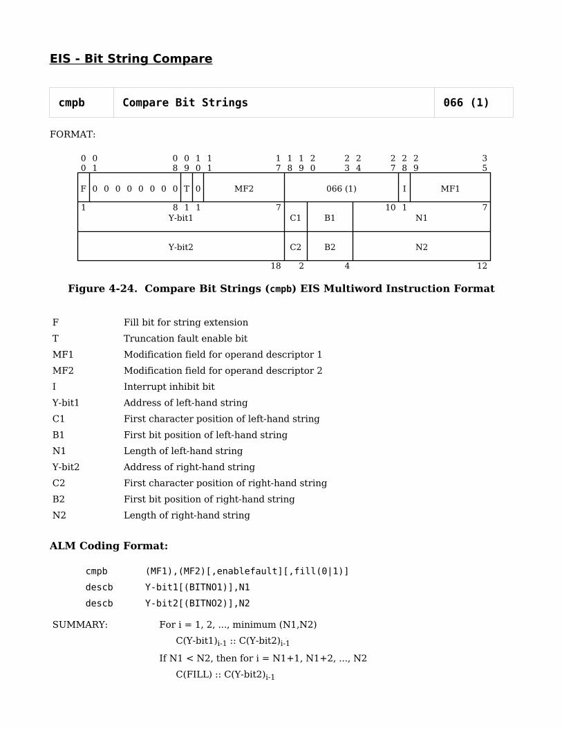
EIS - Bit String Compare
cmpb Compare Bit Strings 066 (1)
FORMAT:
Figure 4-24. Compare Bit Strings (cmpb) EIS Multiword Instruction Format
F Fill bit for string extension
T Truncation fault enable bit
MF1 Modification field for operand descriptor 1
MF2 Modification field for operand descriptor 2
I Interrupt inhibit bit
Y-bit1 Address of left-hand string
C1 First character position of left-hand string
B1 First bit position of left-hand string
N1 Length of left-hand string
Y-bit2 Address of right-hand string
C2 First character position of right-hand string
B2 First bit position of right-hand string
N2 Length of right-hand string
ALM Coding Format:
cmpb (MF1),(MF2)[,enablefault][,fill(0|1)]
descb Y-bit1[(BITNO1)],N1
descb Y-bit2[(BITNO2)],N2
SUMMARY: For i = 1, 2, ..., minimum (N1,N2)
C(Y-bit1)i-1 :: C(Y-bit2)i-1
If N1 < N2, then for i = N1+1, N1+2, ..., N2
C(FILL) :: C(Y-bit2)i-1
00
01
08
09
10
11
17
18
20
23
24
27
28
29
35
F 0 0 0 0 0 0 0 0
8
T
1
0
1
MF2
7
066 (1)
10
I
1
MF1
7Y-bit1 C1 B1 N1
C2
2
B2
4
N2
1218
Y-bit2
19
1
If N1 > N2, then for i = N2+l, N2+2, ..., N1
C(Y-bit1)i-1 :: C(FILL)
MODIFICATIONS: None except au, qu, al, ql, xn for MF1 and MF2
INDICATORS: (Indicators not listed are not affected)
Zero If C(Y-bit1)i = C(Y-bit2)i for all i, then ON; otherwise, OFF
Carry If C(Y-bit1)i < C(Y-bit2)i for any i, then OFF; otherwise ON
NOTES: Instruction execution proceeds until an inequality is found or the larger string length count is exhausted.
If MFk.RL = 1, then Nk does not contain the operand length; instead, it contains a register code for a register holding the operand length.
If MFk.ID = 1, then the kth word following the instruction word does not contain an operand descriptor; instead, it contains an indirect pointer to the operand descriptor.
Attempted execution with the xed instruction causes an illegal procedure fault.
Attempted repetition with the rpt, rpd, or rpl instructions causes an illegal procedure fault.
EIS - Bit String Set Indicators
sztl Set Zero and Truncation Indicators with Bit Strings Left
064 (1)
FORMAT: Same as Combine Bit Strings Left (csl) (see Figure 4-23).
SUMMARY: For i = bits 1, 2, ..., minimum (N1,N2)
m = C(Y-bit1)i-1 || C(Y-bit2)i-1 (a 2-bit number)
If C(BOLR)m ≠ 0, then terminate
If N1 < N2, then for i = N1+i, N1+2, ..., N2
m = C(F) || C(Y-bit2)i-1 (a 2-bit number)
If C(BOLR)m ≠ 0, then terminate
MODIFICATIONS: None except au, qu, al, ql, xn for MF1 and MF2
INDICATORS: (Indicators not listed are not affected)
Zero If C(BOLR)m = 0 for all i, then ON; otherwise OFF
Truncation If N1 > N2, then ON; otherwise OFF
NOTES: If N1 > N2, the low order (N1-N2) bits of C(Y-biti) are not processed and the truncation indicator is set ON.
The execution of this instruction is identical to the Combine Bit Strings Left (csl) instruction except that C(BOLR)m is not placed into C(Y-bit2)i-1.
The bit pattern in C(BOLR) defines the Boolean operation to be performed. Any of the sixteen possible Boolean operations may be used. See NOTES under the Combine Bit Strings Left (csl) instruction for examples of BOLR.
If MFk.RL = 1, then Nk does not contain the operand length; instead, it contains a register code for a register holding the operand length.
If MFk.ID = 1, then the kth word following the instruction word does not contain an operand descriptor; instead, it contains an indirect pointer to the operand descriptor.
If T = 1 and the truncation indicator is set ON by execution of the instruction, then a truncation (overflow) fault occurs.
Attempted execution with the xed instruction causes an illegal procedure fault.
Attempted repetition with the rpt, rpd, or rpl instructions causes an illegal procedure fault.
sztr Set Zero and Truncation Indicators with Bit Strings Right
065 (1)
FORMAT: Same as Combine Bit Strings Left (csl) (see Figure 4-23).

SUMMARY: For i = bits 1, 2, ..., minimum (N1,N2)
m = C(Y-bit1)N1-i || C(Y-bit2)N2-i (a 2-bit number)
If C(BOLR)m ≠ 0, then terminate
If N1 < N2, then for i = N1+1, N1+2, ..., N2
m = C(F) || C(Y-bit2)N2-i (a 2-bit number)
If C(BOLR)m ≠ 0, then terminate
MODIFICATIONS: None except au, qu, al, ql, xn for MF1 and MF2
INDICATORS: (Indicators not listed are not affected)
Zero If C(BOLR)m = 0 for all i, then ON; otherwise OFF
Truncation If N1 > N2, then ON; otherwise OFF
NOTES: If N1 > N2, the low order (N1-N2) bits of C(Y-bit1) are not processed and the truncation indicator is set ON.
The execution of this instruction is identical to the Combine Bit Strings Right (csr) instruction except that C(BOLR)m is not placed into C(Y-bit2)N2-i.
The bit pattern in C(BOLR) defines the Boolean operation to be performed. Any of the sixteen possible Boolean operations may be used. See NOTES under the Combine Bit Strings Left (csl) instruction for examples of BOLR.
If MFk.RL = 1, then Nk does not contain the operand length; instead, it contains a register code for a register holding the operand length.
If MFk.ID = 1, then the kth word following the instruction word does not contain an operand descriptor; instead, it contains an indirect pointer to the operand descriptor.
If T = 1 and the truncation indicator is set ON by execution of the instruction, then a truncation (overflow) fault occurs.
Attempted execution with the xed instruction causes an illegal procedure fault.
Attempted repetition with the rpt, rpd, or rpl instructions causes an illegal procedure fault.
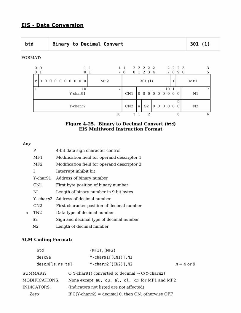
EIS - Data Conversion
btd Binary to Decimal Convert 301 (1)
FORMAT:
Figure 4-25. Binary to Decimal Convert (btd)EIS Multiword Instruction Format
key
P 4-bit data sign character control
MF1 Modification field for operand descriptor 1
MF2 Modification field for operand descriptor 2
I Interrupt inhibit bit
Y-char91 Address of binary number
CN1 First byte position of binary number
N1 Length of binary number in 9-bit bytes
Y- charn2 Address of decimal number
CN2 First character position of decimal number
a TN2 Data type of decimal number
S2 Sign and decimal type of decimal number
N2 Length of decimal number
ALM Coding Format:
btd (MF1),(MF2)
desc9a Y-char91[(CN1)],N1
descn[ls,ns,ts] Y-charn2[(CN2)],N2 n = 4 or 9
SUMMARY: C(Y-char91) converted to decimal C(Y-char→ n2)
MODIFICATIONS: None except au, qu, al, ql, xn for MF1 and MF2
INDICATORS: (Indicators not listed are not affected)
Zero If C(Y-charn2) = decimal 0, then ON: otherwise OFF
00
01
10
11
17
18
20
21
22
23
24
30
27
28
29
35
P
1
0 0 0 0 0 0 0 0 0 0
10
MF2
7
301 (1)
10
I
1
MF1
7Y-char91 CN1 0 0 0 0 0 0 0 0 0
9
N1
CN2
3
a
1
S2
2
0 0 0 0 0 0
6
N2
618
Y-charn2

Negative If a minus sign character is moved to C(Y-charn2), then ON; otherwise OFF
Overflow If fixed-point integer overflow occurs, then ON; otherwise unchanged (see NOTES)
NOTES: C(Y-char91) contains a twos complement binary integer aligned on 9-bit character boundaries with length 0 < N1 <= 8.
If TN2 and S2 specify a 4-bit signed number and P = 1, then if C(Y-char91) is positive (bit 0 of C(Y-char91)0 = 0), then the 138 plus sign character is moved to C(Y-charn2) as appropriate.
The scaling factor of C(Y-charn2), SF2, must be 0.
If N2 is not large enough to hold the digits generated by conversion of C(Y-char91) an overflow condition exists; the overflow indicator is set ON and an overflow fault occurs. This implies that an unsigned fixed-point receiving field has a minimum length of 1 character and a signed fixed-point field, 2 characters.
If MFk.RL = 1, then Nk does not contain the operand length; instead; it contains a register code for a register holding the operand length.
If MFk.ID = 1, then the kth word following the instruction word does not contain an operand descriptor; instead, it contains an indirect pointer to the operand descriptor.
C(Y-char91) and C(Y-charn2) may be overlapping strings; no check is made.
Attempted conversion to a floating-point number (S2 = 0) or attempted use of a scaling factor (SF2 ≠ 0) causes an illegal procedure fault.
If N1 = 0 or N1 > 8 an illegal procedure fault occurs.
Attempted execution with the xed instruction causes an illegal procedure fault.
Attempted repetition with the rpt, rpd, or rpl instructions causes an illegal procedure fault.
dtb Decimal to Binary Convert 305 (1)
FORMAT:
Figure 4-26. Decimal to Binary Convert (dtb)EIS Multiword Instruction Format
00
10
11
17
18
20
21
22
23
24
30
27
28
29
35
0 0 0 0 0 0 0 0 0 0 0
11
MF2
7
305 (1)
10
I
1
MF1
7Y-charn1 CN1 a S1 0 0 0 0 0 0
6
N1
CN2
3
01
0 02
0 0 0 0 0 0
9
N2
618
Y-char92

key
MF1 Modification field for operand descriptor 1
MF2 Modification field for operand descriptor 2
I Interrupt inhibit bit
Y-charn1 Address of decimal number
CN1 First character position of decimal number
a TN1 Data type of decimal number
S1 Sign and decimal type of decimal number
N1 Length of decimal number
Y-char92 Address of binary number
CN2 First byte position of binary number
N2 Length of binary number in 9-bit bytes
ALM Coding Format:
dtb (MF1),(MF2)
descn[ls,ns,ts] Y-charn1[(CN1)],N1 n = 4 or 9
desc9a Y-char92[(CN2)],N2
SUMMARY: C(Y-charn1) converted to binary C(Y-char92)→
MODIFICATIONS: None except au, qu, al, ql, xn for MF1 ad MF2
INDICATORS: (Indicators not listed are not affected)
Zero If C(Y-char92) = 0, then ON: otherwise OFF
Negative If a minus sign character is found in C(Y-charn1), then ON; otherwise OFF
Overflow If fixed-point integer overflow occurs, then ON; otherwise unchanged (see NOTES)
NOTES: C(Y-char92) will contain a twos complement binary integer aligned on 9-bit byte boundaries with length 0 < N2 <= 8.
The scaling factor of C(Y-charn1), SF1, must be 0.
If N2 is not large enough to hold the converted value of C(Y-charn1) an overflow condition exists; the overflow indicator is set ON and an overflow fault occurs.
If MFk.RL = 1, then Nk does not contain the operand length; instead, it contains a register code for a register holding the operand length.
If MFk.ID = 1, then the kth word following the instruction word does not contain an operand descriptor; instead, it contains an indirect pointer to the operand descriptor.
C(Y-charn1) and C(Y-char92) may be overlapping strings; no check is made.
Attempted conversion of a floating-point number (S1 = 0) or attempted use of a scaling factor (SF1 ≠ 0) causes an illegal procedure fault.
If N2 = 0 or N2 > 8 an illegal procedure fault occurs.
Attempted execution with the xed instruction causes an illegal procedure fault.
Attempted repetition with the rpt, rpd, or rpl instructions causes an illegal procedure fault.
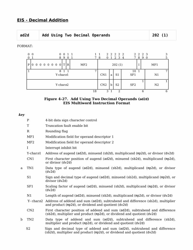
EIS - Decimal Addition
ad2d Add Using Two Decimal Operands 202 (1)
FORMAT:
Figure 4-27. Add Using Two Decimal Operands (ad2d)EIS Multiword Instruction Format
key
P 4-bit data sign character control
T Truncation fault enable bit
R Rounding flag
MF1 Modification field for operand descriptor 1
MF2 Modification field for operand descriptor 2
I Interrupt inhibit bit
Y-charn1 Address of augend (ad2d), minuend (sb2d), multiplicand (mp2d), or divisor (dv2d)
CN1 First character position of augend (ad2d), minuend (sb2d), multiplicand (mp2d), or divisor (dv2d)
a TN1 Data type of augend (ad2d), minuend (sb2d), multiplicand (mp2d), or divisor (dv2d)
S1 Sign and decimal type of augend (ad2d), minuend (sb2d), multiplicand (mp2d), or divisor (dv2d)
SF1 Scaling factor of augend (ad2d), minuend (sb2d), multiplicand (mp2d), or divisor (dv2d)
N1 Length of augend (ad2d), minuend (sb2d), multiplicand (mp2d), or divisor (dv2d)
Y- charn2 Address of addend and sum (ad2d), subtrahend and difference (sb2d), multiplier and product (mp2d), or dividend and quotient (dv2d)
CN2 First character position of addend and sum (ad2d), subtrahend and difference (sb2d), multiplier and product (mp2d), or dividend and quotient (dv2d)
b TN2 Data type of addend and sum (ad2d), subtrahend and difference (sb2d), multiplier and product (mp2d), or dividend and quotient (dv2d)
S2 Sign and decimal type of addend and sum (ad2d), subtrahend and difference (sb2d), multiplier and product (mp2d), or dividend and quotient (dv2d)
00
01
08
09
10
11
17
18
20
21
22
23
24
27
28
29
35
P
1
0 0 0 0 0 0 0 0
8
T
1
R
1
MF2
7
202 (1)
10
I
1
MF1
7Y-charn1 CN1 a S1 SF1
1
N1
1CN2
3
b
1
S2
2
SF2
6
N2
618
Y-charn2
30
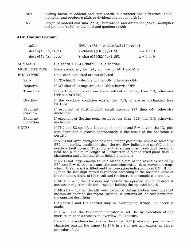
SF2 Scaling factor of addend and sum (ad2d), subtrahend and difference (sb2d), multiplier and product (mp2d), or dividend and quotient (dv2d)
N2 Length of addend and sum (ad2d), subtrahend and difference (sb2d), multiplier and product (mp2d), or dividend and quotient (dv2d)
ALM Coding Format:
ad2d (MF1),(MF2)[,enablefault][,round]
descn[fl,ls,ns,ts] Y-charn1[(CN1)],N1,SF1 n = 4 or 9
descn[fl,ls,ns,ts] Y-charn2[(CN2)],N2,SF2 n = 4 or 9
SUMMARY: C(Y-charn1) + C(Y-charn2) C(Y-char→ n2)
MODIFICATIONS: None except au, qu, al, ql, xn for MF1 and MF2
INDICATORS: (Indicators not listed are not affected)
Zero If C(Y-charn2) = decimal 0, then ON; otherwise OFF
Negative If C(Y-charn2) is negative, then ON; otherwise OFF
Truncation If the truncation condition exists without rounding, then ON; otherwise OFF see NOTES)
Overflow If the overflow condition exists, then ON; otherwise unchanged (see NOTES)
Exponent overflow
If exponent of floating-point result exceeds 127 then ON; otherwise unchanged.
Exponent underflow
If exponent of floating-point result is less than -128 then ON; otherwise unchanged
NOTES: If TN2 and S2 specify a 4-bit signed number and P = 1, then the 138 plus sign character is placed appropriately if the result of the operation is positive.
If N2 is not large enough to hold the integer part of the result as scaled by SF2, an overflow condition exists; the overflow indicator is set ON and an overflow fault occurs. This implies that an unsigned fixed-point receiving field has a minimum length of l character; a signed fixed-point field, 2 characters; and a floating-point field, 3 characters.
If N2 is not large enough to hold all the digits of the result as scaled by SF2 and R = 0, then a truncation condition exists; data movement stops when. C(Y-charn2) is filled and the truncation indicator is set ON. If R = 1, then the last digit moved is rounded according to the absolute value of the remaining digits of the result and the instruction completes normally.
If MFk.RL = 1, then Nk does not contain the operand length; instead, it contains a register code for a register holding the operand length.
If MFk.ID = 1, then the kth word following the instruction word does not contain an operand descriptor; instead, it contains an indirect pointer to the operand descriptor.
C(Y-charn1) and C(Y-charn2) may be overlapping strings; no check is made.
If T = l and the truncation indicator is set ON by execution of the instruction, then a truncation (overflow) fault occurs.
Detection of a character outside the range [0,11]8 in a digit position or a character outside the range [12,17]8 in a sign position causes an illegal procedure fault.

Attempted execution with the xed instruction causes an illegal procedure fault.
Attempted repetition with the rpt, rpd, or rpl instructions causes an illegal procedure fault.
ad3d Add Using Three Decimal Operands 222 (1)
FORMAT:
Figure 4-28. Add Using Three Decimal Operands (ad3d)EIS Multiword Instruction Format
key
P 4-bit data sign character control
T Truncation fault enable bit
R Rounding flag
MF1 Modification field for operand descriptor 1
MF2 Modification field for operand descriptor 2
MF3 Modification field for operand descriptor 3
I Interrupt inhibit bit
Y-charn1 Address of augend (ad3d), minuend (sb3d), multiplicand (mp3d), or divisor (dv3d)
CN1 First character position of augend (ad3d), minuend (sb3d), multiplicand (mp3d), or divisor (dv3d)
a TN1 Data type of augend (ad3d), minuend (sb3d), multiplicand (mp3d), or divisor (dv3d)
S1 Sign and decimal type of augend (ad3d), minuend (sb3d), multiplicand (mp3d), or divisor (dv3d)
SF1 Scaling factor of augend (ad3d), minuend (sb3d), multiplicand (mp3d), or divisor (dv3d)
N1 Length of augend (ad3d), minuend (sb3d), multiplicand (mp3d), or divisor (dv3d)
Y- charn2 Address of addend (ad3d), subtrahend (sb3d), multiplier (mp3d), or dividend (dv3d)
00
01
02
08
09
10
11
17
18
20
21
22
23
24
27
28
29
35
P
1
0
1
MF3
7
T
1
R
1
MF2
7
222 (1)
10
I
1
MF1
7Y-charn1 CN1 a S1 SF1 N1
CN2 b S2 SF2 N2
18
CN3
3
c
1
S3
2
SF3
6
N3
6
Y-charn2
Y-charn3
30
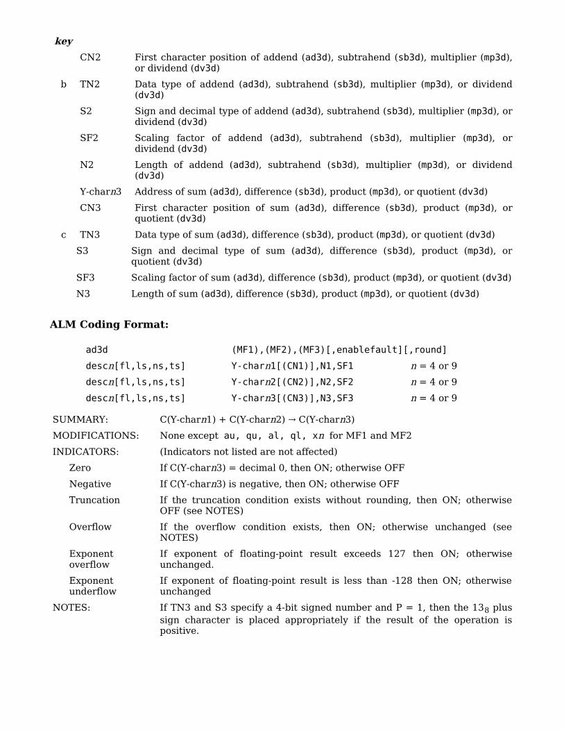
key
CN2 First character position of addend (ad3d), subtrahend (sb3d), multiplier (mp3d), or dividend (dv3d)
b TN2 Data type of addend (ad3d), subtrahend (sb3d), multiplier (mp3d), or dividend (dv3d)
S2 Sign and decimal type of addend (ad3d), subtrahend (sb3d), multiplier (mp3d), or dividend (dv3d)
SF2 Scaling factor of addend (ad3d), subtrahend (sb3d), multiplier (mp3d), or dividend (dv3d)
N2 Length of addend (ad3d), subtrahend (sb3d), multiplier (mp3d), or dividend (dv3d)
Y-charn3 Address of sum (ad3d), difference (sb3d), product (mp3d), or quotient (dv3d)
CN3 First character position of sum (ad3d), difference (sb3d), product (mp3d), or quotient (dv3d)
c TN3 Data type of sum (ad3d), difference (sb3d), product (mp3d), or quotient (dv3d)
S3 Sign and decimal type of sum (ad3d), difference (sb3d), product (mp3d), or quotient (dv3d)
SF3 Scaling factor of sum (ad3d), difference (sb3d), product (mp3d), or quotient (dv3d)
N3 Length of sum (ad3d), difference (sb3d), product (mp3d), or quotient (dv3d)
ALM Coding Format:
ad3d (MF1),(MF2),(MF3)[,enablefault][,round]
descn[fl,ls,ns,ts] Y-charn1[(CN1)],N1,SF1 n = 4 or 9
descn[fl,ls,ns,ts] Y-charn2[(CN2)],N2,SF2 n = 4 or 9
descn[fl,ls,ns,ts] Y-charn3[(CN3)],N3,SF3 n = 4 or 9
SUMMARY: C(Y-charn1) + C(Y-charn2) C(Y-char→ n3)
MODIFICATIONS: None except au, qu, al, ql, xn for MF1 and MF2
INDICATORS: (Indicators not listed are not affected)
Zero If C(Y-charn3) = decimal 0, then ON; otherwise OFF
Negative If C(Y-charn3) is negative, then ON; otherwise OFF
Truncation If the truncation condition exists without rounding, then ON; otherwise OFF (see NOTES)
Overflow If the overflow condition exists, then ON; otherwise unchanged (see NOTES)
Exponent overflow
If exponent of floating-point result exceeds 127 then ON; otherwise unchanged.
Exponent underflow
If exponent of floating-point result is less than -128 then ON; otherwise unchanged
NOTES: If TN3 and S3 specify a 4-bit signed number and P = 1, then the 138 plus sign character is placed appropriately if the result of the operation is positive.

If N3 is not large enough to hold the integer part of the result as scaled by SF3, an overflow condition exists; the overflow indicator is set ON and an overflow fault occurs. This implies that an unsigned fixed-point receiving field has a minimum length of 1 character; a signed fixed-point field, 2 characters; and a floating-point field, 3 characters.
If N3 is not large enough to hold all the digits of the result as scaled by SF3 and R = 0, then a truncation condition exists; data movement stops when C(Y-charn3) is filled and the truncation indicator is set ON. If R = 1, then the last digit moved is rounded according to the absolute value of the remaining digits of the result and the instruction completes normally.
If MFk.RL = 1, then Nk does not contain the operand length; instead, it contains a register code for a register holding the operand length.
If MFk.ID = 1, then the kth word following the instruction word does not contain an operand descriptor; instead, it contains an indirect pointer to the operand descriptor.
C(Y-charn1), C(Y-charn2), and G(Y-charn3) may be overlapping strings; no check is made.
If T = 1 and the truncation indicator is set ON by execution of the instruction, then a truncation (overflow) fault occurs.
Detection of a character outside the range [0,11]8 in a digit position or a character outside the range [12,17]8 in a sign position causes an illegal procedure fault.
Attempted execution with the xed instruction causes an illegal procedure fault.
Attempted repetition with the rpt, rpd, or rpl instructions causes an illegal procedure fault.

EIS - Decimal Subtraction
sb2d Subtract Using Two Decimal Operands 203 (1)
FORMAT: Same as Add Using Two Decimal Operands (ad2d) (see Figure 4-27).
SUMMARY: C(Y-charn1) - C(Y-charn2) C(Y-char→ n2)
MODIFICATIONS: None except au, qu, al, ql, xn for MF1 and MF2
INDICATORS: (Indicators not listed are not affected)
Zero If C(Y-charn2) = decimal 0, then ON; otherwise OFF
Negative If C(Y-charn2) is negative, then ON; otherwise OFF
Truncation If the truncation condition exists without rounding, then ON; otherwise OFF (see NOTES)
Overflow If the overflow condition exists, then ON; otherwise unchanged (see NOTES)
Exponent overflow
If exponent of floating-point result exceeds 127 then ON; otherwise unchanged.
Exponent underflow
If exponent of floating-point result is less than -128 then ON; otherwise unchanged
NOTES: If TN2 and S2 specify a 4-bit signed number and P = 1, then the 138 plus sign character is placed appropriately if the result of the operation is positive.
If N2 is not large enough to hold the integer part of the result as scaled by SF2, an overflow condition exists; the overflow indicator is set ON and an overflow fault occurs. This implies that an unsigned fixed-point receiving field has a minimum length of 1 character; a signed fixed-point field, 2 characters; and a floating-point field, 3 characters.
If N2 is not large enough to hold all the digits of the result as scaled by SF2 and R = 0, then a truncation condition exists; data movement stops when C(Y-charn2) is filled and the truncation indicator is set ON. If R = 1, then the last digit moved is rounded according to the absolute value of the remaining digits of the result and the instruction completes normally.
If MFk.RL = 1, then Nk does not contain the operand length; instead, it contains a register code for a register holding the operand length.
If MFk.ID = 1, then the kth word following the instruction word does not contain an operand descriptor; instead, it contains an indirect pointer to the operand descriptor.
C(Y-charn1) and C(Y-charn2) may be overlapping strings; no check is made.
If T = 1 and the truncation indicator is set ON by execution of the instruction, then a truncation (overflow) fault occurs.
Detection of a character outside the range [0,11]8 in a digit position or a character outside the range [12,17]8 in a sign position causes an illegal procedure fault.
Attempted execution with the xed instruction causes an illegal procedure fault.

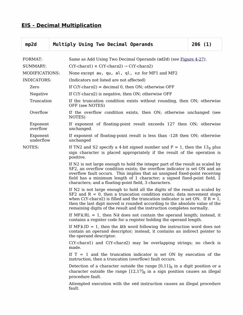
EIS - Decimal Multiplication
mp2d Multiply Using Two Decimal Operands 206 (1)
FORMAT: Same as Add Using Two Decimal Operands (ad2d) (see Figure 4-27).
SUMMARY: C(Y-charn1) × C(Y-charn2) C(Y-char→ n2)
MODIFICATIONS: None except au, qu, al, ql, xn for MF1 and MF2
INDICATORS: (Indicators not listed are not affected)
Zero If C(Y-charn2) = decimal 0, then ON; otherwise OFF
Negative If C(Y-charn2) is negative, then ON; otherwise OFF
Truncation If the truncation condition exists without rounding, then ON; otherwise OFF (see NOTES)
Overflow If the overflow condition exists, then ON; otherwise unchanged (see NOTES)
Exponent overflow
If exponent of floating-point result exceeds 127 then ON; otherwise unchanged.
Exponent underflow
If exponent of floating-point result is less than -128 then ON; otherwise unchanged
NOTES: If TN2 and S2 specify a 4-bit signed number and P = 1, then the 138 plus sign character is placed appropriately if the result of the operation is positive.
If N2 is not large enough to hold the integer part of the result as scaled by SF2, an overflow condition exists; the overflow indicator is set ON and an overflow fault occurs. This implies that an unsigned fixed-point receiving field has a minimum length of 1 character; a signed fixed-point field, 2 characters; and a floating-point field, 3 characters.
If N2 is not large enough to hold all the digits of the result as scaled by SF2 and R = 0, then a truncation condition exists; data movement stops when C(Y-charn2) is filled and the truncation indicator is set ON. If R = 1, then the last digit moved is rounded according to the absolute value of the remaining digits of the result and the instruction completes normally.
If MFk.RL = 1, then Nk does not contain the operand length; instead, it contains a register code for a register holding the operand length.
If MFk.ID = 1, then the kth word following the instruction word does not contain an operand descriptor; instead, it contains an indirect pointer to the operand descriptor.
C(Y-charn1) and C(Y-charn2) may be overlapping strings; no check is made.
If T = 1 and the truncation indicator is set ON by execution of the instruction, then a truncation (overflow) fault occurs.
Detection of a character outside the range [0,11]8 in a digit position or a character outside the range [12,17]8 in a sign position causes an illegal procedure fault.
Attempted execution with the xed instruction causes an illegal procedure fault.

Attempted repetition with the rpt, rpd, or rpl instructions causes an illegal procedure fault.
mp3d Multiply Using Three Decimal Operands 226 (1)
FORMAT: Same as Add Using Three Decimal Operands (ad3d) (see Figure 4-28).
SUMMARY: C(Y-charn1) × C(Y-charn2) C(Y-char→ n3)
MODIFICATIONS: None except au, qu, al, ql, xn for MF1 and MF2
INDICATORS: (Indicators not listed are not affected)
Zero If C(Y-charn3) = decimal 0, then ON; otherwise OFF
Negative If C(Y-charn3) is negative, then ON; otherwise OFF
Truncation If the truncation condition exists without rounding, then ON; otherwise OFF (see NOTES)
Overflow If the overflow condition exists, then ON; otherwise unchanged (see NOTES)
Exponent overflow
If exponent of floating-point result exceeds 127 then ON; otherwise unchanged.
Exponent underflow
If exponent of floating-point result is less than -128 then ON; otherwise unchanged
NOTES: If TN3 and S3 specify a 4-bit signed number and P = 1, then the 138 plus sign character is placed appropriately if the result of the operation is positive.
If N3 is not large enough to hold the integer part of the result as scaled by SF3, an overflow condition exists; the overflow indicator is set ON and an overflow fault occurs. This implies that an unsigned fixed-point receiving field has a minimum length of 1 character; a signed fixed-point field, 2 characters; and a floating-point field, 3 characters.
If N3 is not large enough to hold all the digits of the result as scaled by SF3 and R = 0, then a truncation condition exists; data movement stops when C(Y-charn3) is filled and the truncation indicator is set ON. If R = 1, then the last digit moved is rounded according to the absolute value of the remaining digits of the result and the instruction completes normally.
If MFk.RL = 1, then Nk does not contain the operand length; instead, it contains a register code for a register holding the operand length.
If MFk.ID = 1, then the kth word following the instruction word does not contain an operand descriptor; instead, it contains an indirect pointer to the operand descriptor.
C(Y-charn1), C(Y-charn2), and C(Y-charn3) may be overlapping strings; no check is made.
If T = 1 and the truncation indicator is set ON by execution of the instruction, then a truncation (overflow) fault occurs.
Detection of a character outside the range [0,11]8 in a digit position or a character outside the range [12,17]8 in a sign position causes an illegal procedure fault.
Attempted execution with the xed instruction causes an illegal procedure fault.

Attempted repetition with the rpt, rpd, or rpl instructions causes an illegal procedure fault.

EIS - Decimal Division
dv2d Divide Using Two Decimal Operands 207 (1)
FORMAT: Same as Add Using Two Decimal Operands (ad2d) (see Figure 4-27).
SUMMARY: C(Y-charn2) / C(Y-charn1) C(Y-char→ n2)
MODIFICATIONS: None except au, qu, al, ql, xn for MF1 and MF2
INDICATORS: (Indicators not listed are not affected)
Zero If C(Y-charn2) = decimal 0, then ON; otherwise OFF
Negative If C(Y-charn2) is negative, then ON; otherwise OFF
Overflow If the overflow condition exists, then ON; otherwise unchanged (see NOTES)
Exponent overflow
If exponent of floating-point result exceeds 127 then ON; otherwise unchanged.
Exponent Underflow
If exponent of floating-point result is less than -128 then ON; otherwise unchanged
NOTES: This instruction performs continued long division on the operands until it has produced enough output digits to satisfy the requirements of the quotient field. The number of required quotient digits, NQ, is determined before division begins as follows:
1) Floating-point quotient
NQ = N2, but if the divisor is greater than the dividend after operand alignment, the leading zero digit produced is counted and the effective precision of the result is reduced by one.
2) Fixed-point quotient
NQ = (N2-LZ2+1) - (N1-LZ1) + (E2-E1-SF2)
where: Nn = given operand field length
LZn = leading zero count for operand n
En = exponent of operand n
SF2 = scaling factor of quotient
3) Rounding
If rounding is specified (R = 1), then one extra quotient digit is produced.
If C(Y-charn1) = decimal 0 or NQ > 63, then division does not take place, C(Y-charn2) are unchanged, and a divide check fault occurs.
If TN2 and S2 specify a 4-bit signed number and P = 1, then the 138 plus sign character is placed appropriately if the result of the operation is positive.
If N2 is not large enough to hold the integer part of the result as scaled by SF2, an overflow condition exists; the overflow indicator is set ON and an overflow fault occurs. This implies that an unsigned fixed-point receiving field has a minimum length of 1 character; a signed fixed-point field, 2 characters; and a floating-point field, 3 characters.

If N2 is not large enough to hold all the digits of the result as scaled by SF2 and R = 0, then a truncation condition exists; data movement stops when C(Y-charn2) is filled and the truncation indicator is set ON. If R = 1, then the last digit moved is rounded according to the absolute value of the extra quotient digit and the instruction completes normally.
If MFk.RL = 1, then Nk does not contain the operand length; instead, it contains a register code for a register holding the operand length.
If MFk.ID = 1, then the kth word following the instruction word does not contain an operand descriptor; instead, it contains an indirect pointer to the operand descriptor.
C(Y-charn1) and C(Y-charn2) may be overlapping strings; no check is made.
Detection of a character outside the range [0,11]8 in a digit position or a character outside the range [12,17]8 in a sign position causes an illegal procedure fault.
Attempted execution with the xed instruction causes an illegal procedure fault.
Attempted repetition with the rpt, rpd, or rpl instructions causes an illegal procedure fault.
dv3d Divide Using Three Decimal Operands 227 (1)
FORMAT: Same as Add Using Three Decimal Operands (ad3d) (see Figure 4-28).
SUMMARY: C(Y-charn2) / C(Y-charn1) C(Y-char→ n3)
MODIFICATIONS: None except au, qu, al, ql, xn for MF1 and MF2
INDICATORS: (Indicators not listed are not affected)
Zero If C(Y-charn3) = decimal 0, then ON; otherwise OFF
Negative If C(Y-charn3) is negative, then ON; otherwise OFF
Overflow If the overflow condition exists, then ON; otherwise unchanged (see NOTES)
Exponent overflow
If exponent of floating-point result exceeds 127 then ON; otherwise unchanged.
Exponent underflow
If exponent of floating-point result is less than -128 then ON; otherwise unchanged
NOTES: This instruction performs continued long division on the operands until it has produced enough output digits to satisfy the requirements of the quotient field. The number of required quotient digits, NQ, is determined before division begins as follows:
1) Floating-point quotient
NQ = N3, but if the divisor is greater than the dividend after operand alignment, the leading zero digit produced is counted and the effective precision of the result is reduced by one.
2) Fixed-point quotient
NQ = (N2-LZ2+1) - (N1-LZ1) + (E2-E1-SF3)
where: Nn = given operand field length
LZn = leading zero count for operand n
En = exponent of operand n
SF3 = scaling factor of quotient
3) Rounding
If rounding is specified (R = 1), then one extra quotient digit is produced.
If C(Y-charn1) = decimal 0 or NQ > 63, then division does not take place, C(Y-charn3) are unchanged, and a divide check fault occurs.
If TN3 and S3 specify a 4-bit signed number and P = 1 , then the 138 plus sign character is placed appropriately if the result of the operation is positive.
If N3 is not large enough to hold the integer part of the result as scaled by SF3, an overflow condition exists; the overflow indicator is set ON and an overflow fault occurs. This implies that an unsigned fixed-point receiving field has a minimum length of 1 character; a signed fixed-point field, 2 characters; and a floating-point field, 3 characters.
If N3 is not large enough to hold all the digits of the result as scaled by SF3 and R = 0, then a truncation condition exists; data movement stops when C(Y-charn3) is filled and the truncation indicator is set ON. If R = 1, then the last digit moved is rounded according to the absolute value of the extra quotient digit and the instruction completes normally.
If MFk.RL = 1, then Nk does not contain the operand length; instead, it contains a register code for a register holding the operand length.
If MFk.ID = 1, then the kth word following the instruction word does not contain an operand descriptor; instead, it contains an indirect pointer to the operand descriptor.
C(Y-charn1), G(Y-charn2), and C(Y-charn3) may be overlapping strings; no check is made.
Detection of a character outside the range [0,11]8 in a digit position or a character outside the range [12,17]8 in a sign position causes an illegal procedure fault.
Attempted execution with the xed instruction causes an illegal procedure fault.
Attempted repetition with the rpt, rpd, or rpl instructions causes an illegal procedure fault.

MICRO OPERATIONS FOR EDIT INSTRUCTIONS
The Move Alphanumeric Edited (mve) and Move Numeric Edited (mvne) instructions require micro operations to perform the editing functions in an efficient manner. The sequence of micro operation steps to be executed is contained in main memory and is referenced by the second operand descriptor of the mve or mvne instructions. Some of the micro operations require special characters for insertion into the string of characters being edited. These special characters are shown in the "Edit Insertion Table" discussion below.
Micro Operation Sequence
The micro operation string operand descriptor points to a string of 9-bit bytes that specify the micro operations to be performed during an edited move. Each of the 9-bit bytes defines a micro operation and has the following format:
Figure 4-29. Micro Operation (MOP) Character Format
MOP 5-bit code specifying the micro operator
IF Information field containing one of the following:
1) A sending string character count. A value of 0 is interpreted as 16.
2) The index of an entry in the edit insertion table to be used. Permissible values are 1 through 8.
3) An interpretation of the "blank-when-zero" operation
Edit Insertion Table
While executing an edit instruction, the processor provides a register of eight 9-bit bytes to hold insertion information. This register, called the edit insertion table, is not maintained after execution of an edit instruction. At the start of each edit instruction, the processor initializes the table to the values given in Table 4-8, where each symbol refers to the corresponding standard ASCII character.
Table 4-8. Default Edit Insertion Table Characters
Table Entry Number Character
1 blank
2 *
3 +
4 -
5 $
6 ,
00
MOP
04
5
05
IF
08
4

Table Entry Number Character
7 .
8 0 (zero)
One or all of the table entries can be changed by the Load Table Entry (lte) or the Change Table (cht) micro operations to provide different insertion characters.
Edit Flags
The processor provides the following four edit flags for use by the micro operations.
ES End suppression flag; initially OFF and set ON by a micro operation when zero suppression ends.
SN Sign flag; initially set OFF if the sending string is alphanumeric or unsigned numeric. If the sending string is signed numeric, the sending string sign character is tested and SN is set OFF if positive, and ON if negative.
Z Zero flag; initially set ON. It is set OFF whenever a sending string character that is not decimal zero is moved into the receiving string.
BZ Blank-when-zero flag; initially set OFF and is set ON by either the enf or ses micro operation. If, at the completion of a move, both the Z and BZ are ON, the receiving string is filled with character 1 of the edit insertion table.
Terminating Micro Operations
The micro operation sequence is terminated normally when the receiving string length becomes exhausted. The micro operation sequence is terminated abnormally (with an illegal procedure fault) if a move from an exhausted sending string or the use of an exhausted MOP string is attempted.
MVNE and MVE Differences
The processor executes mvne in a slightly different manner than it executes mve. This is due to the inherent differences in the way numeric and alphanumeric data are handled. The following are brief descriptions of the hardware operations for mvne and mve.
Numeric Edit
1. Load the entire sending string number (maximum length 63 characters) into the decimal unit input buffer as 4-bit digits (high-order truncating 9-bit data). Strip the sign and exponent characters (if any), put them aside into special holding registers and decrease the input buffer count accordingly.
2. Test sign and, if required, set the SN flag.
3. Execute micro operation string, starting with first (4-bit) digit.
4. If an edit insertion table entry or MOP insertion character is to be stored, ANDed, or ORed into a receiving string of 4- or 6-bit characters, high-order truncate the character accordingly.
5. If the receiving string is 9-bit characters, high-order fill the (4-bit) digits from the input buffer with bits 0-4 of character 8 of the edit insertion table. If the receiving string is 6-bit characters, high-order fill the digits with "00"b.

Alphanumeric Edit
1. Load decimal unit input buffer with sending string characters. Data is read from main memory in unaligned units (not modulo 8 boundary) of Y-block8 words. The number of characters loaded is the minimum of the remaining sending string count, the remaining receiving string count, and 64.
2. Execute micro operation string, starting with the first receiving string character.
3. If an edit insertion table entry or MOP insertion character is to be stored, ANDed, or ORed into a receiving string of 4- or 6-bit characters, high-order truncate the character accordingly.
Micro Operations
A description of the 17 micro operations (MOPs) follows. The mnemonic, name, octal value, and the function performed is given for each MOP in a format similar to that for processor instructions. These micro operations are included in the alphabetic list of instructions in Appendix B, identified by the code MOP.
Checks for termination are made during and after each micro operation. All MOPs that make a zero test of a sending string character test only the four least significant bits of the character.
The following additional abbreviations and symbols are used in the description of the MOPs.
EIT edit insertion table
pin current position in the sending string
pmop current position in the micro operation string
pout current position in the receiving string
After each MOP, add one to pmop.
cht Change Table 21
SUMMARY: For i = 1, 2, ..., 8
C(Y-char92)pmop+i C(EIT)→ i
pmop = pmop + 8
FLAGS: None affected
NOTES: C(IF) is not interpreted for this operation.
enf End Floating Suppression 02
SUMMARY: If C(IF)0 = 0, then

If ES is OFF, then
If SN is OFF, then C(EIT)3 C(Y-char→ n3)pout
If SN is ON, then C(EIT)4 C(Y-char→ n3)pout
pout = pout + 1
ES set ON
If ES is ON, then no action
If C(IF)0 = 1, then
If ES is OFF, then
C(EIT)5 C(Y-char→ n3)pout
pout = pout + 1
ES set ON
If ES is ON, then no action
If C(IF)1 = 1, then BZ set ON; otherwise no action
FLAGS: (Flags not listed are not affected)
ES If OFF, then set ON
BZ If C(IF) = 1, then set ON; otherwise no change
ign Ignore Source Character 14
SUMMARY: pin = pin + C(IF)
FLAGS: None affected
insa Insert Asterisk on Suppression 11
SUMMARY: If ES is OFF, then
C(EIT)2 C(Y-char→ n3)pout
If C(IF) = 0, then pmop = pmop
If ES is ON, then
If C(IF) ≠ 0, then
m = C(IF)
C(EIT)m C(Y-char→ n3)pout
If C(IF) = 0, then
C(Y-char92)pmop+1 C(Y-char→ n3)pout
pmop = pmop + 1
pout = pout + 1
FLAGS: None affected
NOTES: If C(IF) > 8 an illegal procedure fault occurs.
insb Insert Blank on Suppression 10
SUMMARY: If ES is OFF, then
C(EIT)1 C(Y-char→ n3)pout
If C(IF) = 0, then pmop = pmop + 1
If ES is ON, then
If C(IF) ≠ 0, then
m = C(IF)
C(EIT)m C(Y-char→ n3)pout
If C(IF) = 0, then
C(Y-char92)pmop+1 C(Y-char→ n3)pout
pmop = pmop + 1
pout = pout + 1
FLAGS: None affected
NOTES: If C(IF) > 8 an illegal procedure fault occurs.
insm Insert Table Entry One Multiple 01
SUMMARY: For i = 0, 1, ..., C(IF) - 1
C(EIT)1 C(Y-char→ n3)pout+i
pout = pout + C(IF)
FLAGS: None affected
insn Insert On Negative 12
SUMMARY: If SN is OFF, then
C(EIT)1 C(Y-char→ n3)pout
If C(IF) = 0, then pmop = pmop + 1
If SN is ON, then
If C(IF) ≠ 0, then
m = C(IF)
C(EIT)m C(Y-char→ n3)pout
If C(IF) = 0, then
C(Y-char92)pmop+1 C(Y-char→ n3)pout
pmop = pmop + 1
pout = pout + 1
FLAGS: None affected
NOTES: If C(IF) > 8 an illegal procedure fault occurs.

insp Insert On Positive 13
SUMMARY: If SN is ON, then
C(EIT)1 C(Y-char→ n3)pout
If C(IF) = 0, then pmop = pmop + 1
If SN is OFF, then
If C(IF) ≠ 0, then
m = C(IF)
C(EIT)m C(Y-char→ n3)pout
If C(IF) = 0, then
C(Y-char92)pmop+1 C(Y-char→ n3)pout
pmop = pmop + 1
pout = pout + 1
FLAGS: None affected
NOTES: If C(IF) > 8 an illegal procedure fault occurs.
lte Load Table Entry 20
SUMMARY: m = C(IF)
C(Y-char92)pmop+1 C(EIT)→ m
pmop = pmop + 1
FLAGS: None affected
NOTES: If C(IF) = 0 or C(IF) > 8 an illegal procedure fault occurs.
mflc Move with Floating Currency Symbol Insertion 07
SUMMARY: For i = 0, 1, ..., C(IF) - 1
If ES is ON, then C(Y-charn1)pin+i C(Y-char→ n3)pout+i
If ES is OFF and C(Y-charn1)pin+i = decimal 0, then
C(EIT)1 C(Y-char→ n3)pout+i
If ES is OFF and C(Y-charn1)pin+i ≠ decimal 0, then
C(EIT)5 C(Y-char→ n3)pout+i
C(Y-charn1)pin+i C(Y-char→ n3)pout+i+1
pout = pout + 1
ES set ON
pin = pin + C(IF)
pout = pout + C(IF)

FLAGS: (Flags not listed are not affected)
ES If OFF and any of C(Y-charn1)pin+i ≠ decimal 0, then ON; otherwise unchanged
Z See the "Edit Flags" section.
NOTES: The number of characters moved to the receiving string is data dependent. If the entire C(Y-charn1) are decimal 0s, C(IF) characters are moved to C(Y-charn3). However, if the sending string contains a non-zero character, then C(IF)+1 characters are moved to C(Y-charn3); the insertion character plus C(Y-charn1). A possible illegal procedure fault due to this condition may be avoided by assuring that the Z and BZ flags are ON.
mfls Move with Floating Sign Insertion 06
SUMMARY: For i = 0, 1, ..., C(IF) - 1
If ES is ON, then C(Y-charn1)pin+i C(Y-char→ n3)pout+i
If ES is OFF and C(Y-charn1)pin+i = decimal 0, then
C(EIT)1 C(Y-char→ n3)pout+i
If ES is OFF and C(Y-charn1)pin+i ≠ decimal 0, then
If SN is OFF, then C(EIT)3 C(Y-char→ n3)pout+i
If SN is ON, then C(EIT)4 C(Y-char→ n3)pout+i
C(Y-charn1)pin+i C(Y-char→ n3)pout+i+1
pout = pout + 1
ES set On
pin = pin + C(IF)
pout = pout + C(IF)
FLAGS: (Flags not listed are not affected)
ES If OFF and any of C(Y-charn1)pin+i ≠ decimal 0, then ON; otherwise unchanged
Z See the "Edit Flags" section
NOTES: The number of characters moved to the receiving string is data dependent. If the entire C(Y-charn1) are decimal 0s, C(IF) characters are moved to C(Y-charn3). However, if the sending string contains a non-zero character, then C(IF)+1 characters are moved to C(Y-charn3); the insertion character plus C(Y-charn1) A possible illegal procedure fault due to this condition may be avoided by assuring that the Z and BZ flags are ON.
mors Move and OR Sign 17
SUMMARY: For i = 0, 1, ..., C(IF) - 1
If SN is OFF, then
C(Y-charn1)pin+i | C(EIT)3 C(Y-char→ n3)pout+i
If SN is ON, then
C(Y-charn1)pin+i | C(EIT)4 C(Y-char→ n3)pout+i
pin = pin + C(IF)
pout = pout + C(IF)
FLAGS: (Flags not listed are not affected)
Z See the "Edit Flags" section
mses Move and Set Sign 16
SUMMARY: For mvne
For i = 0, 1, ..., C(IF) - 1
C(Y-charn1)pin+i C(Y-char→ n3)pout+i
pin = pin + C(IF)
pout = pout + C(IF)
For mve
C(Z) = 0
For i = 0, 1, ..., C(IF) - 1
C(Y-charn1)pin+i C(Y-char→ n3)pout+i
If C(Z) = 0, then
C(Z) = C(Y-charn1)pin+i & C(EIT)3
If C(Z) = 0, then
C(Z) = C(Y-charn1)pin+i & C(EIT)4
If C(Z) ≠ 0, then SN set ON
pin = pin + C(IF)
pout = pout + C(IF)
FLAGS: (Flags not listed are not affected)
SN If C(EIT)4 found in C(Y-charn1), then ON; otherwise no change
Z See the "Edit Flags" section
mvc Move Source Characters 15
SUMMARY: For i = 0, 1, ..., C(IF) - 1
C(Y-charn1)pin+i C(Y-char→ n3)pout+i
pin = pin + C(IF)
pout = pout + C(IF)
FLAGS: (Flags not listed are not affected)
Z See the "Edit Flags" section

mvza Move with Zero Suppression and Asterisk Replacement
05
SUMMARY: For i = 0, 1, ..., C(IF) - 1
If ES is ON, then C(Y-charn1)pin+i C(Y-char→ n3)pout+i
If ES is OFF and C(Y-charn1)pin+i = decimal 0, then
C(EIT)2 C(Y-char→ n3)pout+i
If ES is OFF and C(Y-charn1)pin+i ≠ decimal 0, then
C(Y-charn1)pin+i C(Y-char→ n3)pout+i
ES set On
pin = pin + C(IF)
pout = pout + C(IF)
FLAGS: (Flags not listed are not affected)
ES If OFF and any of C(Y-charn1)pin+i ≠ decimal 0, then ON; otherwise unchanged
Z See the "Edit Flags" section
mvzb Move with Zero Suppression and Blank Replacement
04
SUMMARY: For i = 0, 1, ..., C(IF) - 1
If ES is ON, then C(Y-charn1)pin+i C(Y-char→ n3)pout+i
If ES is OFF and C(Y-charn1)pin+i = decimal 0, then
C(EIT)1 C(Y-char→ n3)pout+i
If ES is OFF and C(Y-charn1)pin+i ≠ decimal 0, then
C(Y-charn1)pin+i C(Y-char→ n3)pout+i
ES set ON
pin = pin + C(IF)
pout = pout + C(IF)
FLAGS: (Flags not listed are not affected)
ES If OFF and any of C(Y-charn1)pin+i ≠ decimal 0, then ON; otherwise unchanged
Z See the "Edit Flags" section
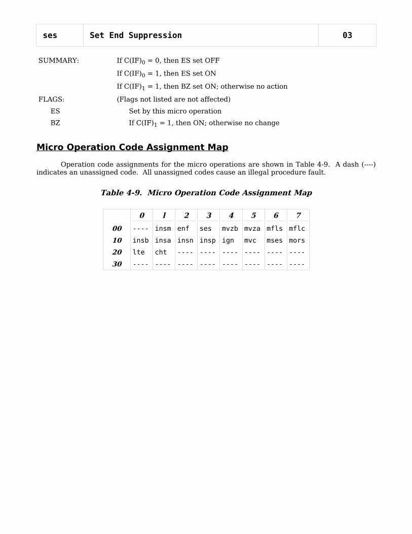
ses Set End Suppression 03
SUMMARY: If C(IF)0 = 0, then ES set OFF
If C(IF)0 = 1, then ES set ON
If C(IF)1 = 1, then BZ set ON; otherwise no action
FLAGS: (Flags not listed are not affected)
ES Set by this micro operation
BZ If C(IF)1 = 1, then ON; otherwise no change
Micro Operation Code Assignment Map
Operation code assignments for the micro operations are shown in Table 4-9. A dash (----) indicates an unassigned code. All unassigned codes cause an illegal procedure fault.
Table 4-9. Micro Operation Code Assignment Map
0 l 2 3 4 5 6 7
00 ---- insm enf ses mvzb mvza mfls mflc
10 insb insa insn insp ign mvc mses mors
20 lte cht ---- ---- ---- ---- ---- ----
30 ---- ---- ---- ---- ---- ---- ---- ----

SECTION 5: ADDRESSING -- SEGMENTATION AND PAGING
ADDRESSING MODES
The Multics processor is able to access the main memory in either absolute mode or append mode. The processor prepares an 18-bit computed address (TPR.CA) for each main memory reference for instructions or operands using the address preparation algorithms described in Section 6. This computed address is a scalar index into a virtual memory with an extent of 262,144 words.
Absolute Mode
In absolute mode, the appending unit is bypassed for instruction fetches and most operand fetches and the final 18-bit computed address (TPR.CA) from address preparation becomes the absolute main memory address.
Thus, all instructions to be executed in absolute mode must reside in the low-order 262,144 words of main memory, that is, main memory addresses 0 through 262,143. Operands normally also reside in the low-order 262,144 words of main memory but, by specifying in an instruction word that the appending unit be used for the main memory access, operands may reside anywhere in main memory. An appended operand fetch may be specified by:
1. Specifying register then indirect (ri) address modification in the instruction word and indirect to segment (its) or indirect to pointer (itp) address modification in the indirect word.
2. Specifying pointer register modification in the instruction word (bit 29 = 1) and giving a pointer register number in the instruction address C(y)0,2.
3. Specifying pointer register modification (MFk.AR = 1) in the modification field for an EIS operand descriptor.
The use of any of the above constructs in absolute mode places the processor in append mode for one or more address preparation cycles. All necessary registers must be properly loaded, all tables of segment descriptor words (SDWs) and page table words (PTWs) expected by the appending unit must exist and be properly described, and all fault conditions must be considered (see append mode below).
If a transfer of control is made with any of the above constructs, the processor remains in append mode after the transfer and subsequent instruction fetches are made in append mode.
Although no segment is defined for absolute mode, it may be helpful to visualize a virtual, unpaged segment overlaying the first 262,144 words of main memory.
Append Mode
In append mode, the appending unit is employed for all main memory references. The appending unit is described later in this section.
SEGMENTATION
In Multics, a segment is defined as an array of arbitrary (but limited) size of machine words containing arbitrary data. A segment is identified within the processor by a segment number (segno) unique to the segment.

To simplify this discussion, the operation of the hardware ring mechanism is not described although it is an integral part of address preparation. See Section 8 for a discussion of the ring mechanism hardware.
A virtual memory address in the processor consists of a pair of integers, (segno,offset) The range of segno is [0,215-1] and the range of offset is [0,218-1]. The description of the segment whose segno value is n is kept in the nth word-pair in a table known as the descriptor segment. The location of the descriptor segment is held by the processor in the descriptor segment base register (DSBR) (see Section 3). Each word-pair of a descriptor segment is known as a segment descriptor word (SDW) and is 72 bits long (see Figure 5-5).
A bit in the SDW for a segment (SDW.U) specifies whether the segment is paged or unpaged. The following is a simplified description of the appending process for unpaged segments (also using an unpaged descriptor segment) (refer to Figures 3-15 and 5-5).
1. If 2 * segno >= 16 * (DSBR.BND + 1), then generate an access violation, out of segment bounds, fault.
2. Fetch the target segment SDW from DSBR.ADDR + 2 * segno.
3. If SDW.F = 0, then generate directed fault n where n is given in SDW.FC. The value of n used here is the value assigned to define a missing segment fault or, simply, a segment fault.
4. If offset >= 16 * (SDW.BOUND + 1), then generate an access violation, out of segment bounds, fault.
5. If the access bits (SDW.R, SDW.E, etc.) of the segment are incompatible with the reference, generate the appropriate access violation fault.
6. Generate 24-bit absolute main memory address SDW.ADDR + offset.
Figure 5-1 depicts the relationships just described.
Figure 5-1. Main Memory Address Generation for Unpaged Segments
PAGING
In Multics, a page is defined as a block of virtual memory with a size of 210 machine words. The processor is designed in such a way that the page size is adjustable over the range [26, 212] but no basis has been found to justify an assertion that any page size is more efficient than 210 or 1024 words.
`SDW SDW(segno)
2 * segno
descriptorsegment
DSBR.ADDR
16 * (DSBR..BND + 1)
`
offset
data
targetsegment
16 * (SDW..BOUND + 1)
The processor divides a k-bit offset or segno value into two parts; the high-order (k-n) bits forming a page number, x, and the low-order n bits forming a word number, y. This may be stated as:
y = (value) modulo (page size)
x = (value - y) / (page size)
The symbols x and y are used in this context throughout this section. An example of page number formation is shown in Figure 5-2.
Figure 5-2. Page Number Formation
A bit in the SDW for a segment (SDW.U) specifies whether the segment is paged or unpaged. A paged segment may be defined as an array of arbitrary (but limited) size of pages and a page may be defined as an array of 1024 machine words. Thus, x is a scalar index into the array of pages, y is a scalar index into the page, and a reference to a word of a paged segment may be treated as a reference to word y of page x of the segment.
Multics subdivides the virtual memory into page size blocks of 1024 words each. Such a subdivision of space allows a segment page to be handled as a physical block independently from the other pages of the segment and from other segments. In main memory, the blocks are known as frames; on secondary storage, they are known as records. When a reference to a word in a paged segment is required (and the page containing the word is not already in main memory), a main memory frame is allocated and the page is read in from secondary storage. Unneeded pages need not occupy space in main memory.
The location and status of page x of a paged segment is kept in the xth word of a table known as the page table for the segment. The words in this table are known as page table words (PTWs) (see Figure 5-6).
Any segment may be paged as appropriate and convenient. The address field of the segment descriptor word (SDW.ADDR) for a paged segment contains the 24-bit absolute main memory address of the page table for the segment instead of the address of the origin of the segment. If the descriptor segment is paged, the address field of the descriptor segment base register (DSBR.ADDR) contains the 24-bit absolute main memory address of the page table for the descriptor segment.
The full algorithm used by the processor to access word offset of paged segment segno (including descriptor segment paging) is as follows. (Refer to Figures 3-15, 5-5, and 5-6.)
1. If 2 * segno >= 16 * (DSBR.BND + 1), then generate an access violation, out of segment bounds, fault.
2. Form the quantities:
y1 = (2 * segno) modulo 1024
00
17
offset
18
00
17
y
10
07
08
8
x

x1 = (2 * segno – y1) / 1024
3. Fetch the descriptor segment PTW(x1) from DSBR.ADR + x1.
4. If PTW(x1).F = 0, then generate directed fault n where n is given in PTW(x1).FC. The value of n used here is the value assigned to define a missing page fault or, simply, a page fault.
5. Fetch the target segment SDW, SDW(segno), from the descriptor segment page at PTW(x1).ADDR + y1.
6. If SDW(segno).F = 0, then generate directed fault n where n is given in SDW(segno).FC. This is a segment fault as discussed earlier in this section.
7. If offset >= 16 * (SDW(segno).BOUND + 1), then generate an access violation, out of segment bounds, fault.
8. If the access bits (SDW(segno).R, SDW(segno).E, etc.) of the segment are incompatible with the reference, generate the appropriate access violation fault.
9. Form the quantities:
y2 = offset modulo 1024
x2 = (offset – y2) / 1024
10.Fetch the target segment PTW(x2) from SDW(segno).ADDR + x2.
11.If PTW(x2).F = 0, then generate directed fault n where n is given in PTW(x2).FC. This is a page fault as in Step 4 above.
12.Generate the 24-bit absolute main memory address PTW(x2).ADDR + y2.
Figure 5-3 depicts the relationships described above.
Figure 5-3. Main Memory Address Generation for Paged Segments
SDW(segno)
`
SDW
descriptorsegment
page
1024
y1
PTW(x2)`PTW
targetsegment
page table
x2`PTW
descriptorsegment
page table
PTW(x1)
x1
DSBR.ADDR
1024
`
data
targetsegment
y2
y1 = (2*segno) modulo 1024x1 = (2 * segno - y1) / 1024y2 = offset modulo 1024x2 = (offset - y2) / 1024

CHANGING ADDRESSING MODES
The processor is placed in absolute mode by the initialize, initialize and clear, or system initialize functions. The first response to faults and interrupts is in absolute mode and the mode thereafter is determined by the instruction sequence entered through the fault or interrupt trap pair. The processor remains in absolute mode until a transfer of control via the appending unit takes place. Note that a Return (ret) or Restore Control Unit (rcu) instruction that sets the absolute indicator OFF (see Section 3 for a discussion of the indicators) or a Return Control Double (rtcd) instruction also places the processor in append mode.
When it responds to a fault or interrupt, the processor enters absolute mode temporarily for the fetch and execution of the trap pair. If an unappended transfer is executed while in the trap pair, the processor remains in absolute mode, otherwise it returns to append mode.
ADDRESS APPENDING
At the completion of the formation of the virtual memory address (see Section 6) an effective segment number (segno) is in the segment number register of the temporary pointer register (TPR.SNR) and a computed address (offset) is in the computed address register of the temporary pointer register (TPR.CA). (See Section 3 for a discussion of the temporary pointer register.)
Address Appending Sequences
Once segno and offset are formed in TPR.SNR and TPR.CA, respectively, the process of generating the 24-bit absolute main memory address can involve a number of different and distinct appending unit cycles.
The operation of the appending unit is shown in the flowchart in Figure 5-4. This flowchart assumes that directed faults, store faults, and parity faults do not occur.
A segment boundary check is made in every cycle except PSDW. If a boundary violation is detected, an access violation, out of segment bounds, fault is generated and the execution of the instruction interrupted. The occurrence of any fault interrupts the sequence at the point of occurrence. The operating system software should store the control unit data for possible later continuation and attempt to resolve the fault condition.
The value of the associative memories may be seen in the flowchart by observing the number of appending unit cycles bypassed if an SDW or PTW is found in the associative memories.
There are nine different appending unit cycles that involve accesses to main memory. Two of these (FANP, FAP) generate the 24-bit absolute main memory address and initiate a main memory access for the operand, indirect word, or instruction pair; five (NSDW, PSDW, PTW, PTW2, and DSPTW) generate a main memory access to fetch an SDW or PTW; and two (MDSPTW and MPTW) generate a main memory access to update page status bits (PTW.U and PTW.M) in a PTW. The cycles are defined in Table 5-1.
Table 5-1. Appending Unit Cycle Definitions
Cycle name Function
FANP Final address nonpaged
Generates the 24-bit absolute main memory address and initiates a main memory access to an unpaged segment for operands, indirect words, or instructions.
FAP Final address paged
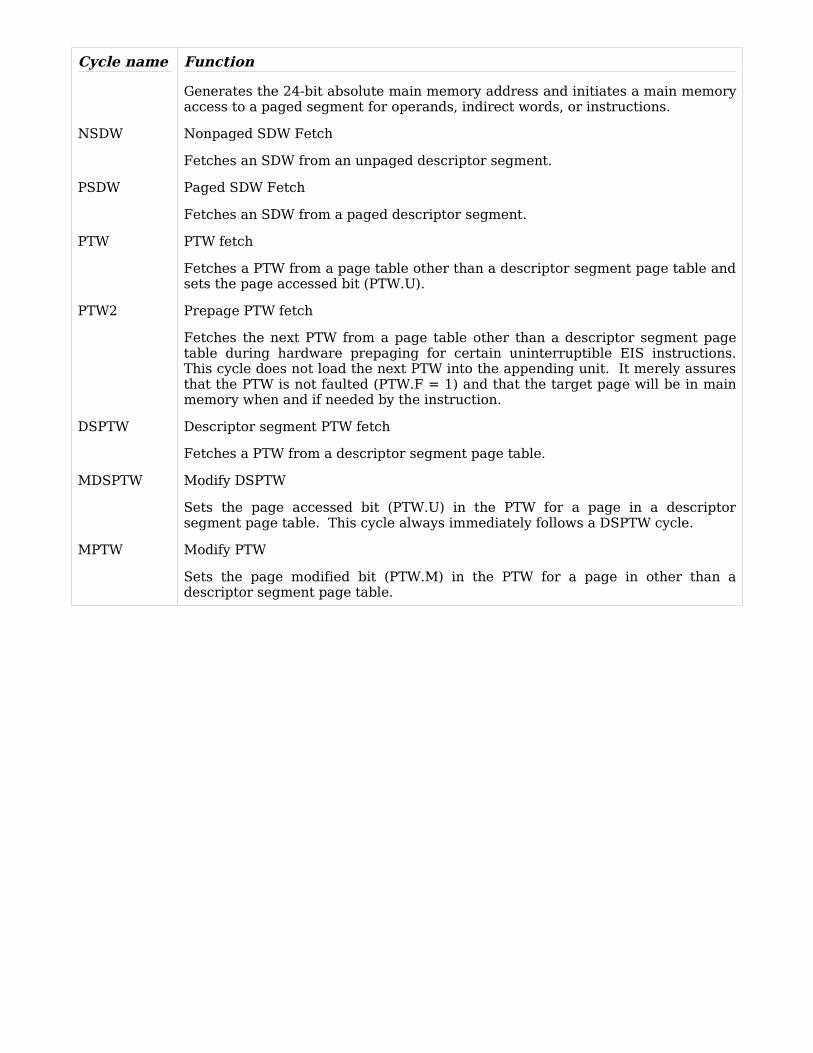
Cycle name Function
Generates the 24-bit absolute main memory address and initiates a main memory access to a paged segment for operands, indirect words, or instructions.
NSDW Nonpaged SDW Fetch
Fetches an SDW from an unpaged descriptor segment.
PSDW Paged SDW Fetch
Fetches an SDW from a paged descriptor segment.
PTW PTW fetch
Fetches a PTW from a page table other than a descriptor segment page table and sets the page accessed bit (PTW.U).
PTW2 Prepage PTW fetch
Fetches the next PTW from a page table other than a descriptor segment page table during hardware prepaging for certain uninterruptible EIS instructions. This cycle does not load the next PTW into the appending unit. It merely assures that the PTW is not faulted (PTW.F = 1) and that the target page will be in main memory when and if needed by the instruction.
DSPTW Descriptor segment PTW fetch
Fetches a PTW from a descriptor segment page table.
MDSPTW Modify DSPTW
Sets the page accessed bit (PTW.U) in the PTW for a page in a descriptor segment page table. This cycle always immediately follows a DSPTW cycle.
MPTW Modify PTW
Sets the page modified bit (PTW.M) in the PTW for a page in other than a descriptor segment page table.

Figure 5-4. Appending Unit Operation Flowchart
APPENDING UNIT DATA WORD FORMATS
Segment Descriptor Word (SDW) Format
The segment descriptor word (SDW) pair contains information that controls the access to a segment. The SDW for segment n is located at offset 2n in the descriptor segment whose description is currently loaded into the descriptor segment base register (DSBR).
START APPEND
YesNo
No
Yes
No
Yes
No
YesNo
Yes
Yes
No
Yes
No
END APPEND
DSPTWcycle
PSDWcycle
NSDWcycle
LoadSDWAM
MDSPTWcycle
FAPcycle
MPTWcycle
PTW2cycle
PTWcycle
FANPcycle
is SDW inSDWAM?
is segmentpaged?
is PTW inPTWAM?
Prepagemode?
STR-OP &PTW.M = 0
is descriptorsegment paged?
is DSPTW.Uset on?
Note: A STR-OP is any processor functionthat writes data to main memory.
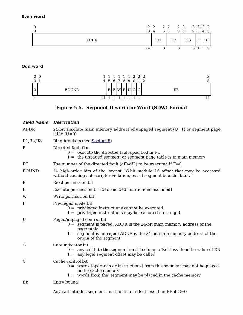
Even word
Odd word
Figure 5-5. Segment Descriptor Word (SDW) Format
Field Name Description
ADDR 24-bit absolute main memory address of unpaged segment (U=1) or segment page table (U=0)
R1,R2,R3 Ring brackets (see Section 8)
F Directed fault flag0 = execute the directed fault specified in FC1 = the unpaged segment or segment page table is in main memory
FC The number of the directed fault (df0-df3) to be executed if F=0
BOUND 14 high-order bits of the largest 18-bit modulo 16 offset that may be accessed without causing a descriptor violation, out of segment bounds, fault.
R Read permission bit
E Execute permission bit (xec and xed instructions excluded)
W Write permission bit
P Privileged mode bit0 = privileged instructions cannot be executed1 = privileged instructions may be executed if in ring 0
U Paged/unpaged control bit0 = segment is paged; ADDR is the 24-bit main memory address of the
page table1 = segment is unpaged; ADDR is the 24-bit main memory address of the
origin of the segment
G Gate indicator bit0 = any call into the segment must be to an offset less than the value of EB1 = any legal segment offset may be called
C Cache control bit0 = words (operands or instructions) from this segment may not be placed
in the cache memory1 = words from this segment may be placed in the cache memory
EB Entry bound
Any call into this segment must be to an offset less than EB if G=0
00
23
ADDR
24
24
R1
26
3
27
R2
29
3
30
R3
32
3
33
F
35
FC
2
34
1
00
0
1
01
14
BOUND
14
15
R
1
16
E
1
17
W
1
18
P
1
19
U
1
20
G
1
21
C
1
22
35
ER
14
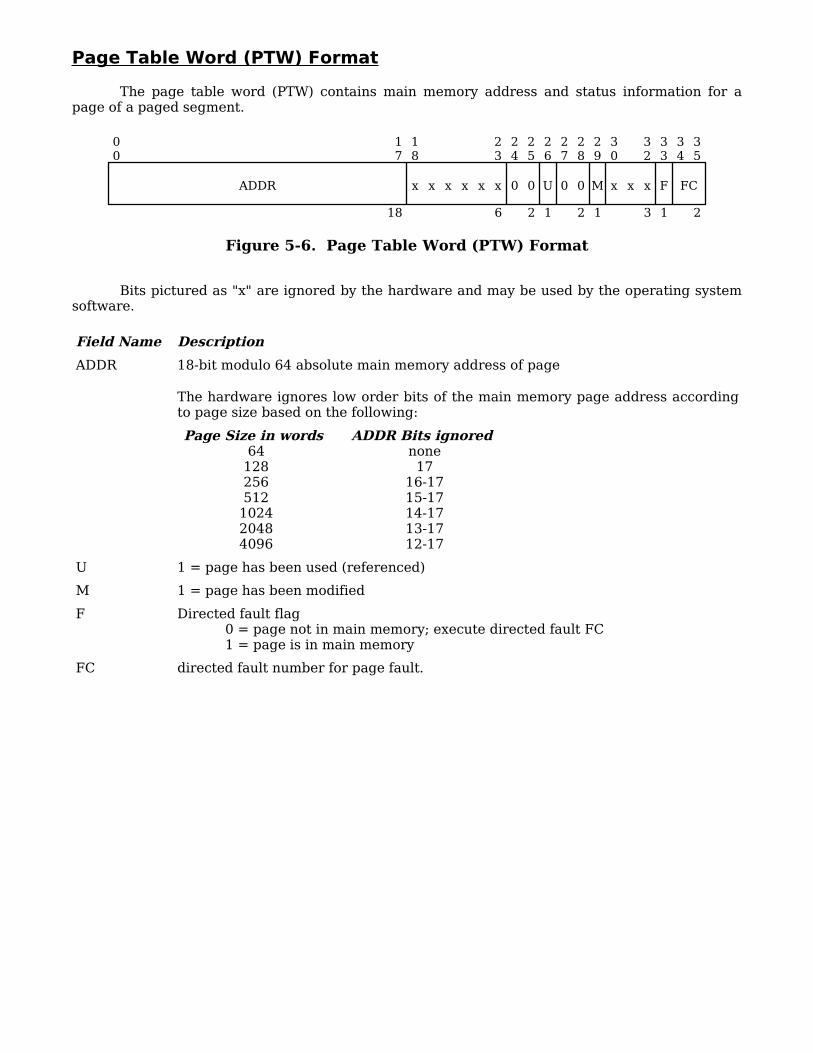
Page Table Word (PTW) Format
The page table word (PTW) contains main memory address and status information for a page of a paged segment.
Figure 5-6. Page Table Word (PTW) Format
Bits pictured as "x" are ignored by the hardware and may be used by the operating system software.
Field Name Description
ADDR 18-bit modulo 64 absolute main memory address of page
The hardware ignores low order bits of the main memory page address according to page size based on the following:
Page Size in words 64
128256512
102420484096
ADDR Bits ignored none17
16-1715-1714-1713-1712-17
U 1 = page has been used (referenced)
M 1 = page has been modified
F Directed fault flag0 = page not in main memory; execute directed fault FC1 = page is in main memory
FC directed fault number for page fault.
00
17
ADDR
18
18
x x x x x
23
x
6
24
0
25
0
2
26
U
1
27
0
28
0
2
29
M
1
30
x x
32
x
3
33
F
1
34
35
FC
2

SECTION 6: VIRTUAL ADDRESS FORMATION
DEFINITION OF VIRTUAL ADDRESS
The virtual address in the Multics processor is the user's specification of the location of a data item in the Multics virtual memory. Each reference to the virtual memory for operands, indirect words, indirect pointers, operand descriptors, or instructions must provide a virtual address. The hardware and the operating system translate the virtual address into the true location of the data item and assure that the data item is in main memory for the reference.
The virtual address consists of two parts, an effective segment number and an offset or computed address. The value of each part is the result of the evaluation of a hardware algorithm (expression) of one or more terms. The selection of the algorithm is made by the use of control bits in the instruction word; for example, bit 29 for modification by pointer register and bits 30-35 (the TAG field) for modification by index register or indirect word. For certain modifications by indirect word, the TAG field of the indirect word is also treated as an address modifier, thus establishing a continuing "indirect chain". Bit 29 of an indirect word has no meaning in the context of virtual address formation.
The results of evaluation of the virtual address formation algorithms are stored in temporary registers used as working registers by the processor. The effective segment number is stored in the temporary segment register, TPR.TSR. The offset is stored in the computed address register, TPR.CA. When each virtual address computation has been completed, C(TPR.TSR) and C(TPR.CA) are presented to the appending unit for translation to a 24-bit absolute main memory address (see Section 5).
TYPES OF VIRTUAL ADDRESS FORMATION
There are two types of virtual address formation. The first type does not make explicit use of segment numbers. The algorithms produce values for the computed address, C(TPR.CA), only. The effective segment number in C(TPR.TSR) does not change from the value used to fetch the current instruction. In this case, all references are said to be "local" to the procedure segment pointed to by the procedure pointer register (PPR).
The second type makes use of a segment number in an indirect word-pair in main memory or in a pointer register (PRn). The algorithms produce values for both the effective segment number, C(TPR.TSR), and the computed address, C(TPR.CA). The effective segment number in C(TPR.TSR) may change and, if it changes, references are said to be "external" to the procedure segment.
Both types of virtual address formation for the operand of a basic or EIS single-word instruction begin with a preliminary step of loading TPR.CA with the ADDRESS field of the instruction word. This preliminary step takes place during instruction decode.
The two types of virtual address formation can be intermixed. In cases where virtual address calculations are chained together through pointer registers or indirect words, each virtual address is translated to a 24-bit absolute main memory address to fetch the next item in the chain.
This description of virtual address formation is divided into two parts corresponding to the two types. The first part describes the type that involves only the computed address, C(TPR.CA). The effective segment number is constant. In append mode its value is equal to C(PPR.PSR) (a local reference) and in absolute mode its value is undefined.
The second part describes the type that involves both the effective segment number, C(TPR.TSR), and the computed address, C(TPR.CA).
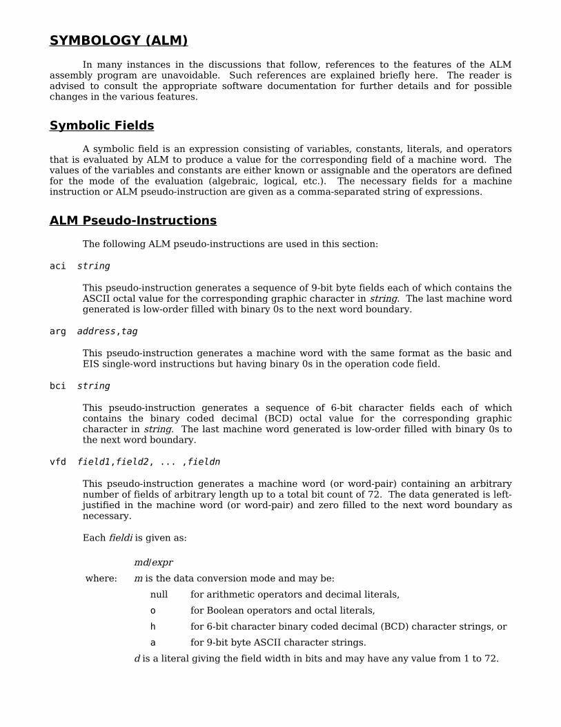
SYMBOLOGY (ALM)
In many instances in the discussions that follow, references to the features of the ALM assembly program are unavoidable. Such references are explained briefly here. The reader is advised to consult the appropriate software documentation for further details and for possible changes in the various features.
Symbolic Fields
A symbolic field is an expression consisting of variables, constants, literals, and operators that is evaluated by ALM to produce a value for the corresponding field of a machine word. The values of the variables and constants are either known or assignable and the operators are defined for the mode of the evaluation (algebraic, logical, etc.). The necessary fields for a machine instruction or ALM pseudo-instruction are given as a comma-separated string of expressions.
ALM Pseudo-Instructions
The following ALM pseudo-instructions are used in this section:
aci string
This pseudo-instruction generates a sequence of 9-bit byte fields each of which contains the ASCII octal value for the corresponding graphic character in string. The last machine word generated is low-order filled with binary 0s to the next word boundary.
arg address,tag
This pseudo-instruction generates a machine word with the same format as the basic and EIS single-word instructions but having binary 0s in the operation code field.
bci string
This pseudo-instruction generates a sequence of 6-bit character fields each of which contains the binary coded decimal (BCD) octal value for the corresponding graphic character in string. The last machine word generated is low-order filled with binary 0s to the next word boundary.
vfd field1,field2, ... ,fieldn
This pseudo-instruction generates a machine word (or word-pair) containing an arbitrary number of fields of arbitrary length up to a total bit count of 72. The data generated is left-justified in the machine word (or word-pair) and zero filled to the next word boundary as necessary.
Each fieldi is given as:
md/expr
where: m is the data conversion mode and may be:
null for arithmetic operators and decimal literals,
o for Boolean operators and octal literals,
h for 6-bit character binary coded decimal (BCD) character strings, or
a for 9-bit byte ASCII character strings.
d is a literal giving the field width in bits and may have any value from 1 to 72.

expr is the expression to be evaluated or converted. Conversion is done with full 36-bit precision and the field value is the conversion result modulo the field width.
COMPUTED ADDRESS FORMATION
The address formation algorithms described here produce values only for the computed address. The effective segment number is constant and equal to C(PPR.PSR) if the processor is in append mode or is undefined if the processor is in absolute mode.
The Address Modifier (TAG) Field
Bits 30-35 of an instruction word or indirect word constitute the address modifier or TAG field. The format of the TAG field is:
Figure 6-1. Address Modifier (TAG) Field Format
Field Name Function
Tm modifier field, specifies one of four general types of computed address modification
Td designator field, selects among several variations available for the general type given with Tm
General Types of Computed Address Modification
There are four general types of computed address modification: register, register then indirect, indirect then register, and indirect then tally. The general types are described in Table 6-1. The value loaded into TPR.CA is symbolized by "y" in the descriptions following.
Table 6-1. General Computed Address Modification Types
Tm value Type Description
0 Register (r)
The contents of the register specified in C(Td) are added to the current computed address, C(TPR.CA), to form the modified computed address. Addition is twos complement, modulo 218, and overflow does not occur.
1 Register then indirect (ri)
The contents of the register specified in C(Td) are added to the current computed address, C(TPR.CA), to form the modified computed address as for register modification. The modified C(TPR.CA) is then used to fetch an indirect word. The TAG field of the indirect word specifies the next step in computed address formation. The use of du or dl as the designator in this modification type will cause an illegal procedure, illegal modifier, fault.
30
35
Td
4
31
32
2
Tm

Tm value Type Description
2 Indirect then tally (it)
The indirect word at C(TPR.CA) is fetched and the modification performed according to the variation specified in C(Td) of the instruction word and the contents of the indirect word. This modification type allows automatic incrementing and decrementing of addresses and tally counting.
3 Indirect then register (ir)
The register designator, C(Td), is safe-stored in a special holding register, CT-HOLD. The word at C(TPR.CA) is fetched and interpreted as an indirect word. The TAG field of the indirect word specifies the next step in computed address formation as follows:
Indirect TAG Next step
r or it Perform register modification using Td from CT-HOLD.(1)
ri Perform the register then indirect modification immediately and fetch the next indirect word from the result of that modification.
ir Replace the safe-stored Td value in CT-HOLD with the Td value from the indirect word TAG field and use the ADDRESS field of the indirect word as a computed address value to fetch the next indirect word.
(1)In this instance, the indirect then tally variations fault tag 1, fault tag 2, and fault tag 3 are treated differently. The fault tag 1 variation results in the action described here but fault tag 2 and fault tag 3 result in the generation of a fault. See the discussion of indirect then tally modification later in this section.
Computed Address Formation Flowcharts
The flowcharts depicting the computed address formation process are scattered throughout this section and are linked together by figure references. The flowcharts start with Figure 6-2.
Figure 6-2. Common Computed Address Formation Flowchart
Register (r) Modification
In register modification (Tm = 0) the value of Td designates a register whose contents are to be added to C(TPR.CA) to form a modified C(TPR.CA). This modified C(TPR.CA) becomes the computed address of the operand. See Figure 6-3, Table 6-2, and the examples following.
START CA
RI MODR MOD IR MODIT MOD
Tm=r Tm=ri Tm=it Tm=ir
(Figure 6-3) (Figure 6-4) (Figure 6-5) (Figure 6-6)
`
InterpretTm

Figure 6-3. Register Modification Flowchart
Table 6-2. Register Modification Decode
Td value Register
Coding Symbol Computed Address
0 none n, null y
1 A0,17 au y + C(A)0,17
2 Q0,17 qu y + C(Q)0,17
3 none du none; y becomes the upper 18 bits of the 36-bit zero filled operand
4 PPR.IC ic y +C(PPR.IC)
5 A18,35 al y +C(A)18,35
6 Q18,35 ql y +C(Q)18,35
7 none dl none; y becomes the lower 18 bits of the 36-bit zero filled operand
10 X0 0, x0 y +C(X0)
11 X1 1, x1 y +C(X1)
12 X2 2, x2 y +C(X2)
13 X3 3, x3 y +C(X3)
14 X4 4, x4 y +C(X4)
15 X5 5, x5 y +C(X5)
16 X6 6, x6 y +C(X6)
17 X7 7, x7 y +C(X7)
R MOD
Yes
Yes
No
END CA
No
r = TdC(TPR.CA) + C(r ) C(TPR.CA)→
Set direct operand flagForm operand
Td = 0?
Td = 3or 7?

Examples:
Location Instruction Computed address
1. a lda y y
2. a sta y,n y
3. a ldaq y,au y + C(A)0,17
4. a tra 3,ic a + 3
5. a ldq y,du none; operand has the form y || (00...0)18
6. a lxl4 y,dl none; operand has the form (00...0)18 || y
7. a mpy y,1 y + C(X1)
8. a stx4 y,7 y + C(X7)
Register Then Indirect (ri) Modifications
In register then indirect modification (Tm = 1) the value of Td designates a register whose contents are to be added to C(TPR.CA) to form a modified C(TPR.CA). This modified C(TPR.CA) is used as a computed address to fetch an indirect word. The ADDRESS field of the indirect word is loaded into TPR.CA and the TAG field of the indirect word is interpreted in the next step of an indirect chain. The TALLY field of the indirect word is ignored.
The indirect chain continues until an indirect word TAG field specifies a modification without indirection.
The coding symbol for register then indirect modification is r* where r is any of the coding symbols for register modification as given in Table 6-1 above except du and dl. The du and dl register codes are illegal and and their use causes an illegal procedure, illegal modifier, fault. See Figure 6-4, Table 6-1, and the examples following.
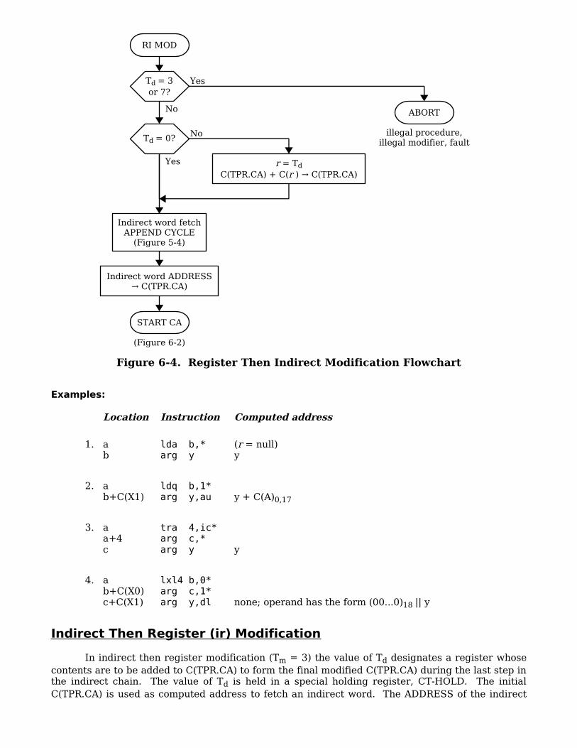
Figure 6-4. Register Then Indirect Modification Flowchart
Examples:
Location Instruction Computed address
1. a lda b,* (r = null)b arg y y
2. a ldq b,1*b+C(X1) arg y,au y + C(A)0,17
3. a tra 4,ic*a+4 arg c,*c arg y y
4. a lxl4 b,0*b+C(X0) arg c,1*c+C(X1) arg y,dl none; operand has the form (00...0)18 || y
Indirect Then Register (ir) Modification
In indirect then register modification (Tm = 3) the value of Td designates a register whose contents are to be added to C(TPR.CA) to form the final modified C(TPR.CA) during the last step in the indirect chain. The value of Td is held in a special holding register, CT-HOLD. The initial C(TPR.CA) is used as computed address to fetch an indirect word. The ADDRESS of the indirect
RI MOD
Yes
Yes
No
START CA
No ABORT
illegal procedure,illegal modifier, fault
(Figure 6-2)
Td = 3or 7?
Td = 0?
r = TdC(TPR.CA) + C(r ) C(TPR.CA)→
Indirect word fetchAPPEND CYCLE
(Figure 5-4)
Indirect word ADDRESS → C(TPR.CA)
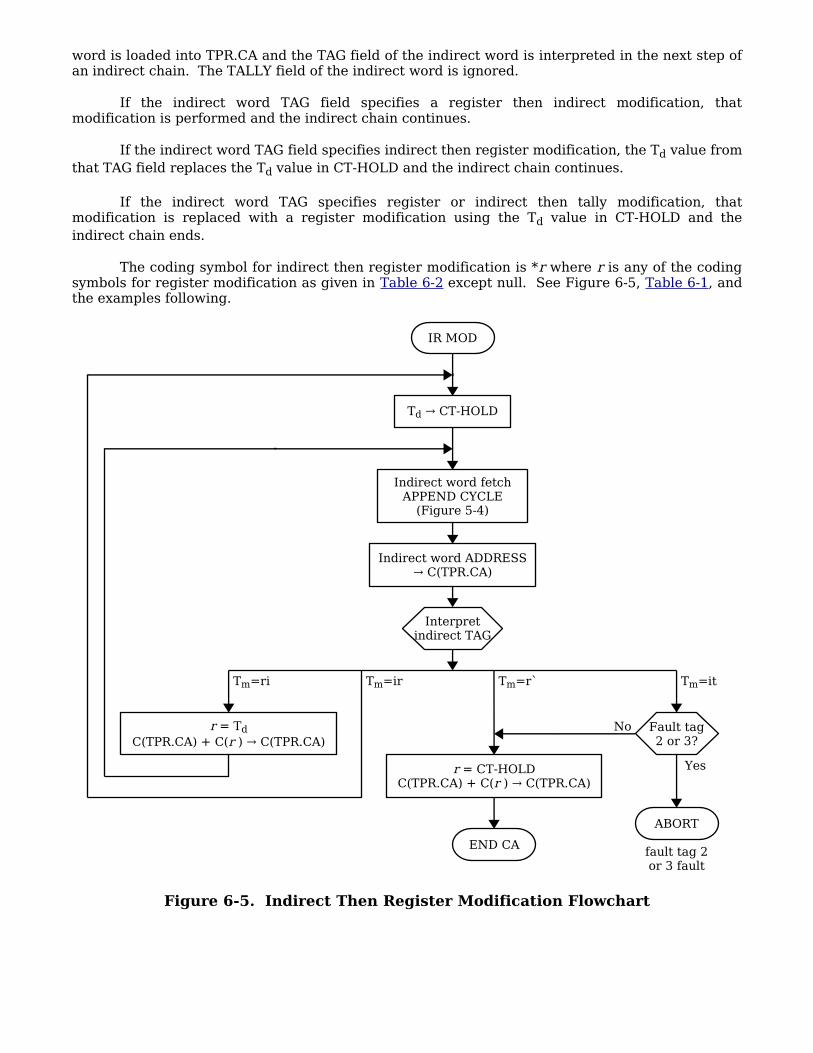
word is loaded into TPR.CA and the TAG field of the indirect word is interpreted in the next step of an indirect chain. The TALLY field of the indirect word is ignored.
If the indirect word TAG field specifies a register then indirect modification, that modification is performed and the indirect chain continues.
If the indirect word TAG field specifies indirect then register modification, the Td value from that TAG field replaces the Td value in CT-HOLD and the indirect chain continues.
If the indirect word TAG specifies register or indirect then tally modification, that modification is replaced with a register modification using the Td value in CT-HOLD and the indirect chain ends.
The coding symbol for indirect then register modification is *r where r is any of the coding symbols for register modification as given in Table 6-2 except null. See Figure 6-5, Table 6-1, and the examples following.
Figure 6-5. Indirect Then Register Modification Flowchart
IR MOD
Yes
No
END CA fault tag 2or 3 fault
ABORT
Tm=ri Tm=ir Tm=r` Tm=it
Td CT-HOLD→
Indirect word fetchAPPEND CYCLE
(Figure 5-4)
Indirect word ADDRESS → C(TPR.CA)
Interpretindirect TAG
Fault tag2 or 3?
r = CT-HOLDC(TPR.CA) + C(r ) C(TPR.CA)→
r = TdC(TPR.CA) + C(r ) C(TPR.CA)→
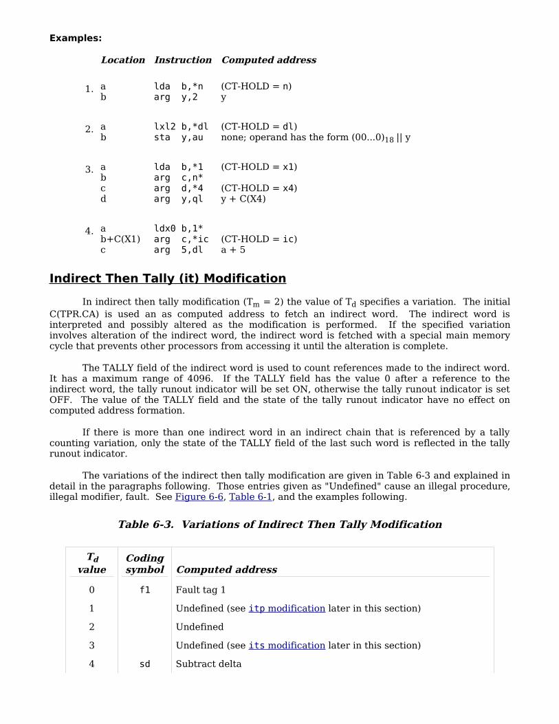
Examples:
Location Instruction Computed address
1. a lda b,*n (CT-HOLD = n)b arg y,2 y
2. a lxl2 b,*dl (CT-HOLD = dl)b sta y,au none; operand has the form (00...0)18 || y
3. a lda b,*1 (CT-HOLD = x1)b arg c,n*c arg d,*4 (CT-HOLD = x4)d arg y,ql y + C(X4)
4. a ldx0 b,1*b+C(X1) arg c,*ic (CT-HOLD = ic)c arg 5,dl a + 5
Indirect Then Tally (it) Modification
In indirect then tally modification (Tm = 2) the value of Td specifies a variation. The initial C(TPR.CA) is used an as computed address to fetch an indirect word. The indirect word is interpreted and possibly altered as the modification is performed. If the specified variation involves alteration of the indirect word, the indirect word is fetched with a special main memory cycle that prevents other processors from accessing it until the alteration is complete.
The TALLY field of the indirect word is used to count references made to the indirect word. It has a maximum range of 4096. If the TALLY field has the value 0 after a reference to the indirect word, the tally runout indicator will be set ON, otherwise the tally runout indicator is set OFF. The value of the TALLY field and the state of the tally runout indicator have no effect on computed address formation.
If there is more than one indirect word in an indirect chain that is referenced by a tally counting variation, only the state of the TALLY field of the last such word is reflected in the tally runout indicator.
The variations of the indirect then tally modification are given in Table 6-3 and explained in detail in the paragraphs following. Those entries given as "Undefined" cause an illegal procedure, illegal modifier, fault. See Figure 6-6, Table 6-1, and the examples following.
Table 6-3. Variations of Indirect Then Tally Modification
Td value
Coding symbol Computed address
0 f1 Fault tag 1
1 Undefined (see itp modification later in this section)
2 Undefined
3 Undefined (see its modification later in this section)
4 sd Subtract delta

Td value
Coding symbol Computed address
5 scr Sequence character reverse
6 f2 Fault tag 2
7 f3 Fault tag 3
10 ci Character indirect
11 i Indirect
12 sc Sequence character
13 ad Add delta
14 di Decrement address, increment tally
15 dic Decrement address, increment tally, and continue
16 id Increment address, decrement tally
17 idc Increment address, decrement tally, and continue
Fault tag 1 (Td = 0)
If this variation appears in an indirect word and the TAG of the instruction word or preceding indirect word is indirect then register (ir), then terminate computed address formation with a register (r) modification using the register held in CT-HOLD. If this variation appears in an instruction word or in an indirect word and the TAG of the instruction word or preceding indirect word is not indirect then register (ir), then generate a fault tag 1 fault.
C(TPR.CA) at the time of the fault contains the computed address of the word containing the fault tag 1 variation. Thus, the ADDRESS and TALLY fields of that word may contain information relative to recovery from the fault.
Subtract delta (Td = 4)
The TAG field of the indirect word is interpreted as a 6-bit, unsigned, positive address increment value, delta. For each reference to the indirect word, the ADDRESS field is reduced by delta and the TALLY field is increased by 1 before the computed address is formed. ADDRESS arithmetic is modulo 218. TALLY arithmetic is modulo 4096. If the TALLY field overflows to 0, the tally runout indicator is set ON, otherwise it is set OFF. The computed address is the value of the decremented ADDRESS field of the indirect word.
Example:
Location Instruction Reference count
Computed address
Tally value
a lda b,sd 1 c-d t+lb vfd 18/c,12/t,6/d 2 c-2d t+2
3 c-3d t+3...n c-nd t+n
Sequence character reverse (Td = 5)
Bit 30 of the TAG field of the indirect word is interpreted as a character size flag, tb, with the value 0 indicating 6-bit characters and the value 1 indicating 9-bit bytes. Bits 33-35 of
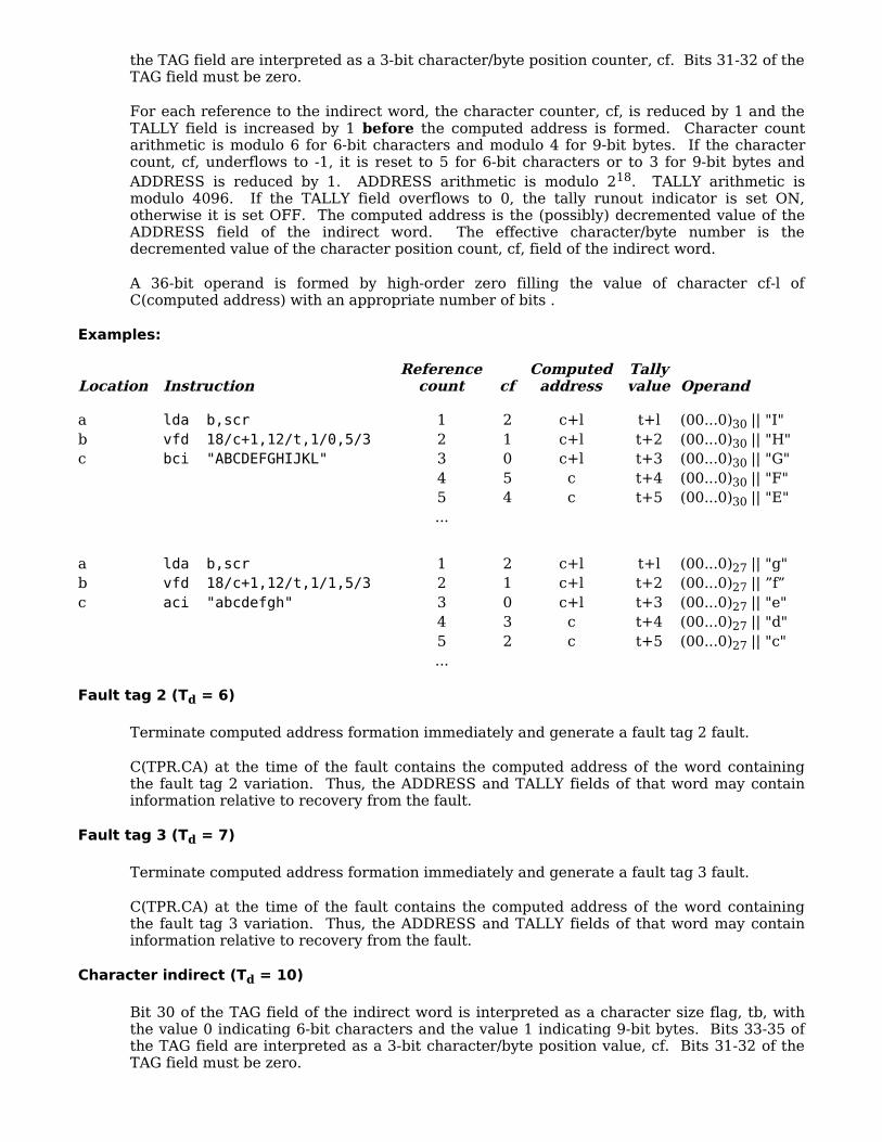
the TAG field are interpreted as a 3-bit character/byte position counter, cf. Bits 31-32 of the TAG field must be zero.
For each reference to the indirect word, the character counter, cf, is reduced by 1 and the TALLY field is increased by 1 before the computed address is formed. Character count arithmetic is modulo 6 for 6-bit characters and modulo 4 for 9-bit bytes. If the character count, cf, underflows to -1, it is reset to 5 for 6-bit characters or to 3 for 9-bit bytes and ADDRESS is reduced by 1. ADDRESS arithmetic is modulo 218. TALLY arithmetic is modulo 4096. If the TALLY field overflows to 0, the tally runout indicator is set ON, otherwise it is set OFF. The computed address is the (possibly) decremented value of the ADDRESS field of the indirect word. The effective character/byte number is the decremented value of the character position count, cf, field of the indirect word.
A 36-bit operand is formed by high-order zero filling the value of character cf-l of C(computed address) with an appropriate number of bits .
Examples:
Location InstructionReference
count cfComputed address
Tally value Operand
a lda b,scr 1 2 c+l t+l (00...0)30 || "I"b vfd 18/c+1,12/t,1/0,5/3 2 1 c+l t+2 (00...0)30 || "H"c bci "ABCDEFGHIJKL" 3 0 c+l t+3 (00...0)30 || "G"
4 5 c t+4 (00...0)30 || "F"5 4 c t+5 (00...0)30 || "E"...
a lda b,scr 1 2 c+l t+l (00...0)27 || "g"b vfd 18/c+1,12/t,1/1,5/3 2 1 c+l t+2 (00...0)27 || ”f”c aci "abcdefgh" 3 0 c+l t+3 (00...0)27 || "e"
4 3 c t+4 (00...0)27 || "d"5 2 c t+5 (00...0)27 || "c"...
Fault tag 2 (Td = 6)
Terminate computed address formation immediately and generate a fault tag 2 fault.
C(TPR.CA) at the time of the fault contains the computed address of the word containing the fault tag 2 variation. Thus, the ADDRESS and TALLY fields of that word may contain information relative to recovery from the fault.
Fault tag 3 (Td = 7)
Terminate computed address formation immediately and generate a fault tag 3 fault.
C(TPR.CA) at the time of the fault contains the computed address of the word containing the fault tag 3 variation. Thus, the ADDRESS and TALLY fields of that word may contain information relative to recovery from the fault.
Character indirect (Td = 10)
Bit 30 of the TAG field of the indirect word is interpreted as a character size flag, tb, with the value 0 indicating 6-bit characters and the value 1 indicating 9-bit bytes. Bits 33-35 of the TAG field are interpreted as a 3-bit character/byte position value, cf. Bits 31-32 of the TAG field must be zero.
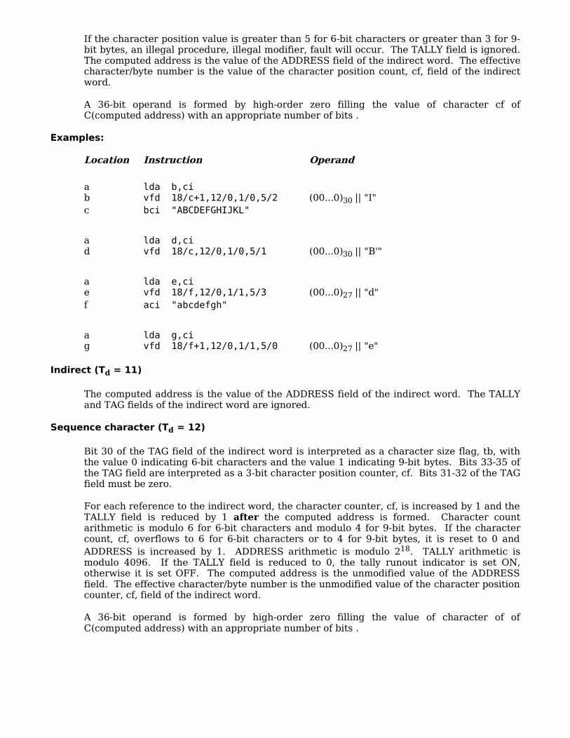
If the character position value is greater than 5 for 6-bit characters or greater than 3 for 9-bit bytes, an illegal procedure, illegal modifier, fault will occur. The TALLY field is ignored. The computed address is the value of the ADDRESS field of the indirect word. The effective character/byte number is the value of the character position count, cf, field of the indirect word.
A 36-bit operand is formed by high-order zero filling the value of character cf of C(computed address) with an appropriate number of bits .
Examples:
Location Instruction Operand
a lda b,cib vfd 18/c+1,12/0,1/0,5/2 (00...0)30 || "I"c bci "ABCDEFGHIJKL"
a lda d,cid vfd 18/c,12/0,1/0,5/1 (00...0)30 || "B'"
a lda e,cie vfd 18/f,12/0,1/1,5/3 (00...0)27 || "d"f aci "abcdefgh"
a lda g,cig vfd 18/f+1,12/0,1/1,5/0 (00...0)27 || "e"
Indirect (Td = 11)
The computed address is the value of the ADDRESS field of the indirect word. The TALLY and TAG fields of the indirect word are ignored.
Sequence character (Td = 12)
Bit 30 of the TAG field of the indirect word is interpreted as a character size flag, tb, with the value 0 indicating 6-bit characters and the value 1 indicating 9-bit bytes. Bits 33-35 of the TAG field are interpreted as a 3-bit character position counter, cf. Bits 31-32 of the TAG field must be zero.
For each reference to the indirect word, the character counter, cf, is increased by 1 and the TALLY field is reduced by 1 after the computed address is formed. Character count arithmetic is modulo 6 for 6-bit characters and modulo 4 for 9-bit bytes. If the character count, cf, overflows to 6 for 6-bit characters or to 4 for 9-bit bytes, it is reset to 0 and ADDRESS is increased by 1. ADDRESS arithmetic is modulo 218. TALLY arithmetic is modulo 4096. If the TALLY field is reduced to 0, the tally runout indicator is set ON, otherwise it is set OFF. The computed address is the unmodified value of the ADDRESS field. The effective character/byte number is the unmodified value of the character position counter, cf, field of the indirect word.
A 36-bit operand is formed by high-order zero filling the value of character of of C(computed address) with an appropriate number of bits .

Examples:
Location InstructionReference
count cfComputed address
Tally value Operand
a lda b,sc 1 4 c t-1 (00...0)30 || "E"b vfd 18/c,12/t,1/0,5/4 2 5 c t-2 (00...0)30 || "F"c bci "ABCDEFGHIJKL" 3 0 c+l t-3 (00...0)30 || "G"
4 1 c+l t-4 (00...0)30 || "H"5 2 c+l t-5 (00...0)30 || "I"...
a lda b,sc 1 2 c t-1 (00...0)27 || "c"b vfd 18/c,12/t,1/1,5/2 2 3 c t-2 (00...0)27 || "d"c aci "abcdefgh" 3 0 c+l t-3 (00...0)27 || "e"
4 1 c+l t-4 (00...0)27 || "f"5 2 c+l t-5 (00...0)27 || "g"...
Add delta (Td = 13)
The TAG field of the indirect word is interpreted as a 6-bit, unsigned, positive address increment value, delta. For each reference to the indirect word, the ADDRESS field is increased by delta and the TALLY field is reduced by 1 after the computed address is formed. ADDRESS arithmetic is modulo 218. TALLY arithmetic is modulo 4096. If the TALLY field is reduced to 0, the tally runout indicator is set ON, otherwise it is set OFF. The computed address is the value of the unmodified ADDRESS field of the indirect word.
Example:
Location Instruction Reference count Computed address
Tally value
a lda b,ad 1 c t-1b vfd 18/c,1/t,6/d 2 c+d t-2
3 c+2d t-3...n c+(n-l)d t-n
Decrement address, increment tally (Td = 14)
For each reference to the indirect word, the ADDRESS field is reduced by 1 and the TALLY field is increased by 1 before the computed address is formed. ADDRESS arithmetic is modulo 218. TALLY arithmetic is modulo 4096. If the TALLY field overflows to 0, the tally runout indicator is set ON, otherwise it is set OFF. The TAG field of the indirect word is ignored. The computed address is the value of the decremented ADDRESS field.
Example:
Location Instruction Reference count
Computed address
Tally value
a lda b,di 1 c-1 t+lb vfd 18/c,12/t 2 c-2 t+2
3 c-3 t+3...n c-n t+n
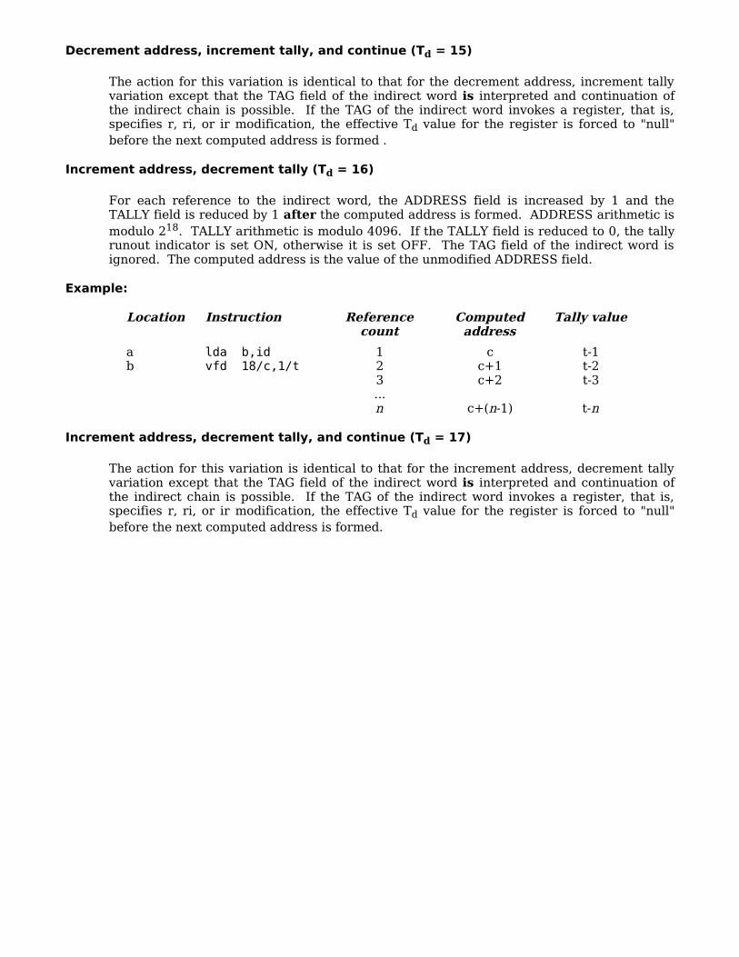
Decrement address, increment tally, and continue (Td = 15)
The action for this variation is identical to that for the decrement address, increment tally variation except that the TAG field of the indirect word is interpreted and continuation of the indirect chain is possible. If the TAG of the indirect word invokes a register, that is, specifies r, ri, or ir modification, the effective Td value for the register is forced to "null" before the next computed address is formed .
Increment address, decrement tally (Td = 16)
For each reference to the indirect word, the ADDRESS field is increased by 1 and the TALLY field is reduced by 1 after the computed address is formed. ADDRESS arithmetic is modulo 218. TALLY arithmetic is modulo 4096. If the TALLY field is reduced to 0, the tally runout indicator is set ON, otherwise it is set OFF. The TAG field of the indirect word is ignored. The computed address is the value of the unmodified ADDRESS field.
Example:
Location Instruction Reference count
Computed address
Tally value
a lda b,id 1 c t-1b vfd 18/c,1/t 2 c+1 t-2
3 c+2 t-3...n c+(n-1) t-n
Increment address, decrement tally, and continue (Td = 17)
The action for this variation is identical to that for the increment address, decrement tally variation except that the TAG field of the indirect word is interpreted and continuation of the indirect chain is possible. If the TAG of the indirect word invokes a register, that is, specifies r, ri, or ir modification, the effective Td value for the register is forced to "null" before the next computed address is formed.

Figure 6-6. Indirect Then Tally Modification Flowchart
VIRTUAL ADDRESS FORMATION INVOLVING BOTH SEGMENT NUMBER AND COMPUTED ADDRESS
The second type of virtual address formation generates an effective segment number and a computed address simultaneously.
The Use of Bit 29 in the Instruction Word
The reader is reminded that there is a preliminary step of loading TPR.CA with the ADDRESS field of the instruction word during instruction decode.
If bit 29 of the instruction word is set to 1, modification by pointer register is invoked and the preliminary step is executed as follows:
1. The ADDRESS field of the instruction word is interpreted as shown in Figure 6-7 below.
2. C(PRn.SNR) C(TPR.TSR)→
IT MOD
Yes
No
???cf field, and
ADDRESS. Formcomputed address
END CA
ABORT
fault tag 1,2, or 3 fault
Td = 0, 6, 7(f1, f2, f3)
Td = 1, 2, 3(undef)
Td = 10, 12, 5(ci, sc, scr)
Td = 11, 13, 4, 14, 16(i, ad, sd, di, id)
Td = 15, 17(dic, idc)
ABORT
illegal procedure,illegal modifier, fault
START CA
Tm = r Tm = ir or it Tm = ri
(Figure 6-2)
InterpretTd
is the cfvalue legal?
Interpretindirect TAG
Indirect word fetchAPPEND CYCLE
(Figure 5-4)
Indirect word fetchAPPEND CYCLE
(Figure 5-4)
Indirect word fetchAPPEND CYCLE
(Figure 5-4)
Indirect word fetchAPPEND CYCLE
(Figure 5-4)
Adjust TALLYand form
computed address
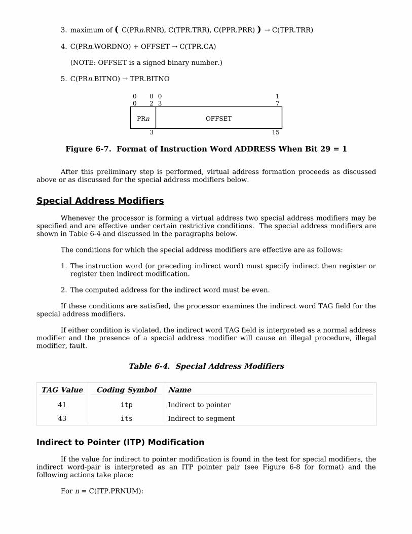
3. maximum of ( C(PRn.RNR), C(TPR.TRR), C(PPR.PRR) ) C(TPR.TRR)→
4. C(PRn.WORDNO) + OFFSET C(TPR.CA)→
(NOTE: OFFSET is a signed binary number.)
5. C(PRn.BITNO) TPR.BITNO→
Figure 6-7. Format of Instruction Word ADDRESS When Bit 29 = 1
After this preliminary step is performed, virtual address formation proceeds as discussed above or as discussed for the special address modifiers below.
Special Address Modifiers
Whenever the processor is forming a virtual address two special address modifiers may be specified and are effective under certain restrictive conditions. The special address modifiers are shown in Table 6-4 and discussed in the paragraphs below.
The conditions for which the special address modifiers are effective are as follows:
1. The instruction word (or preceding indirect word) must specify indirect then register or register then indirect modification.
2. The computed address for the indirect word must be even.
If these conditions are satisfied, the processor examines the indirect word TAG field for the special address modifiers.
If either condition is violated, the indirect word TAG field is interpreted as a normal address modifier and the presence of a special address modifier will cause an illegal procedure, illegal modifier, fault.
Table 6-4. Special Address Modifiers
TAG Value Coding Symbol Name
41 itp Indirect to pointer
43 its Indirect to segment
Indirect to Pointer (ITP) Modification
If the value for indirect to pointer modification is found in the test for special modifiers, the indirect word-pair is interpreted as an ITP pointer pair (see Figure 6-8 for format) and the following actions take place:
For n = C(ITP.PRNUM):
00
17
OFFSET
15
02
03
3
PRn
C(PRn.SNR) C(TPR.TSR)→
maximum of ( C(PRn.RNR), C(SDW.R1), C(TPR.TRR) ) C(TPR.TRR)→
C(ITP.BITNO) C(TPR.TBR)→
C(PRn.WORDNO) + C(ITP.WORDNO) + C(r) C(TPR.CA)→
where:
1. r = C(CT-HOLD) if the instruction word or preceding indirect word specified indirect then register modification, or
2. r = C(ITP.MOD.Td) if the instruction word or preceding indirect word specified register then indirect modification and ITP.MOD.Tm specifies either register or register then indirect modification.
3. SDW.R1 is the upper limit of the read/write ring bracket for the segment C(TPR.TSR) (see Section 8).
Even word
Odd word
Figure 6-8. ITP Pointer Pair Format
Field Name Meaning
PRNUM The number of the pointer register through which to make the segment reference
WORDNO A word offset value to be added to C(PRn.WORDNO)
BITNO A bit offset value for the data item
MOD Any normal address modifier (not ITP or ITS)
Indirect to Segment (ITS) Modification
If the value for indirect to segment modification is found in the test for special modifiers, the indirect word-pair is interpreted as an ITS pointer pair (see Figure 6-9 for format) and the following actions take place:
C(ITS.SEGNO) C(TPR.TSR)→
00
PRNUM
02
3
03
0 0 0 0 0 0 0 0 0 0 0 0 0 0 0 0 0 0 0 0 0 0 0 0 0 0
29
0
27
30
418
35
6
00
17
WORDNO
18
18
0 0
20
0
3
21
26
BITNO
6
27
0 0
29
0
3
30
MOD
31
2
32
Td
35
4TmTm
maximum of ( C(ITS. RN), C(SDW.R1), C(TPR.TRR) ) C(TPR.TRR)→
C(ITS.BITNO) C(TPR.TBR)→
C(ITS.WORDNO) + C(r) C(TPR.CA)→
where:
1. r = C(CT-HOLD) if the instruction word or preceding indirect word specified indirect then register modification, or
2. r = C(ITS.MOD.Td) if the instruction word or preceding indirect word specified register then indirect modification and ITS.MOD.Tm specifies either register or register then indirect modification.
3. SDW.R1 is the upper limit of the read/write ring bracket for the segment C(TPR.TSR) (see Section 8).
Even word
Odd word
Figure 6-9. ITS Pointer Pair Format
Field Name Meaning
SEGNO The number of the segment to be referenced
WORDNO Word offset to be used in the computed address formation
BITNO The bit offset for the data item
MOD Any valid normal address modifier (not ITS or ITP)
Effective Segment Number Generation
A simplified flowchart for effective segment number generation is given in Figure 6-10. Although effective ring number generation and access checking are an integral part of this process, their treatment is deferred to Section 8.
00
0 0
02
0
3
03
17
SEGNO
15
18
RN
20
3
21
0 0 0 0 0 0 0 0
29
0
9
30
438
35
6
00
17
WORDNO
18
18
0 0
20
0
3
21
26
BITNO
6
27
0 0
29
0
3
30
MOD
31
2
32
Td
35
4TmTm

Figure 6-10. Effective Segment Generation Flowchart
START ESN
Yes
No
Yes
No
Yes
No
Yes
No
Yes
No
BA
C(PPR.PSR) C(TPR.TSR)→n = C(instruction word)0,2
C(PRn .SNR) C(TPR.TSR)→
CA CYCLE(Figure 6-2)
Was last cycle anindirect word?
Is bit29 ON?
Was it asequential instruction
fetch?
Indirectword fetch?
ri or ir &TPR.CA even?

Figure 6-10(cont). Effective Segment Number Generation Flowchart
VIRTUAL ADDRESS FORMATION FOR EXTENDED INSTRUCTION SET
The steps involved in virtual address formation for the operand of an EIS instruction are shown in Figure 6-11. The flowchart depicts the virtual address formation for operand k as described by its modification field, MFk. This virtual address formation is performed for each operand as its operand descriptor is decoded.
START ESN
YesNo
BA
Yes
No
Yes
No
Yes
No
Yes
No
Yes
No
EXECUTE
END ESN
appendingunit data
movement?
C(Y)3,17 C(TPR.TSR)→C(Y+1)0,17 C(TPR.CA)→
C(ITS.MOD) TAG→
n = C(Y)0,2C(PRn .SNR) C(TPR.TSR)→
C(PRn .WORDNO) + C(Y+1)0,17 → C(TPR.CA)
C(ITP.MOD) TAG→
C(Y)3,17 C(PPR.PSR)→C(Y+1)0,17 C(PPR.IC)→
C(TPR.TSR) C(PPR.PSR)→C(TPR.CA) C(PPR.IC)`→
TAG =ITS?
TAG =ITP?
Need anindirect word?
rtcdoperand?
call6 ortransfer
operand?
(Not shown)

Figure 6-11. EIS Virtual Address Formation Flowchart
NOTE 1: The symbol "Y" stands for the contents of the ADDRESS field of the operand descriptor. The symbols '"CN" and "C" stand for the contents of the character number field. The symbol "B" stands for the contents of the bit number field.
NOTE 2: The algorithms used in the formation of the effective word/char/bit address are described below.
Character- and Bit-String Addressing
The processor represents the effective address of a character- or bit-string operand in three different forms as follows:
1. Pointer register form
This form consists of a word value (PRn.WORDNO) and a bit value (PRn.BITNO). The word value is the word offset of the word containing the first character or bit of the operand and the bit value is the bit position of that character or bit within the word. This
START EIS CA
YesNo
END EIS CA
YesNo
Yes No
ESN CYCLE(Figure 6-10)
operand descriptorAPPEND CYCLE
(Figure 5-4)
MFk .AR= 1?
MFk .REG= 0?
MFk .ID= 1?
n = C(Y)0,2(NOTE 1)
n = null
r = null r = Mfk .REG
Form effective word/char/bitaddress from
Y, CN, C, B, C(PRn), C(r )(NOTE 1, 2)
form is seen when C(PRn) are stored as an ITS pointer pair or as a packed pointer (see discussion of ITS pointers earlier in this section and the Store Pointer Register n Packed (sprpn) instruction in Section 4).
2. Address register form
This form consists of a word value (ARn.WORDNO), a byte number (ARn.CHAR), and a bit value (ARn.BITNO). The word value is the word offset of the word containing the first character or bit of the operand. The byte number is the number of the 9-bit byte containing the first character or bit. The bit value is the bit position within ARn.CHAR of the first character or bit. This form is seen when C(ARn) are stored with the Store Address Register n (sarn) instruction (see Section 4).
3. Operand Descriptor Form
This form is valid for character-string operands only. It consists of a word value (ADDRESS) and a character number (CN). The word value is the word offset of the word containing the first character of the operand and the character number is the number of that character within the word. This form is seen when C(ARn) are stored with the Address Register n to Alphanumeric Descriptor (aran) or Address Register n to Numeric Descriptor (arnn) instructions. (The operand descriptor form for bit-string operands is identical to the address register form.)
The terms "pointer register" and "address register" both apply to the same physical hardware. The distinction arises from the manner in which the register is used and in the interpretation of the register contents. "Pointer register" refers to the register as used by the appending unit and "address register" refers to the register as used by the decimal unit.
The three forms are compatible and may be freely intermixed. For example, PRn may be loaded in pointer register form with the Effective Pointer to Pointer Register n (eppn) instruction, then modified in pointer register form with the Effective Address to Word/Bit Number of Pointer Register n (eawpn) instruction, then further modified in address register form (assuming character size k) with the Add k-Bit Displacement to Address Register (akbd) instruction, and finally invoked in operand descriptor form by the use of MF.AR in an EIS multiword instruction .
Character- and Bit-String Address Arithmetic Algorithms
The arithmetic algorithms for calculating character- and bit-string addresses are presented below. The symbols "ADDRESS" and "CN" represent the ADDRESS and CN fields of the operand descriptor being decoded. "r" and "n" are set according to the flowchart in Figure 6-11. If either has the value "null", the contents of all associated fields are identically zero.
9-bit Byte String Address Arithmetic
Effective BITNO = 0000
Effective CHAR = (CN + C(ARn.CHAR) + C(r))[4]
Effective WORDNO = ADDRESS + C(ARn.WORDNO) +(CN + C(ARn.CHAR) + C(r)) / 4
6-bit Character String Address Arithmetic
Effective BITNO = (9*C(ARn.CHAR) + 6*C(r) + C(ARn.BITNO))[9]
Effective CHAR = ((9*C(ARn.CHAR) + 6*C(r) + C(ARn.BITNO))[36]) / 9
Effective WORDNO = ADDRESS + C(ARn.WORDNO) +(9*C(ARn.CHAR) + 6*C(r) + C(ARn.BITNO)) / 36
4-bit Byte String Address Arithmetic
Effective BITNO = 4 * (C(ARn.CHAR) + 2*C(r) + C(ARn.BITNO)/4)[2] + 1
Effective CHAR = ((9*C(ARn.CHAR) + 4*C(r) + C(ARn.BITNO))[36] / 9
Effective WORDNO = ADDRESS + C(ARn.WORDNO) +(9*C(ARn.CHAR) + 4*C(r) + C(ARn.BITNO)) / 36
Bit String Address Arithmetic
Effective BITNO = (9*C(ARn.CHAR) + 36*C(r) + C(ARn.BITNO))[9]
Effective CHAR = ((9*C(ARn.CHAR) + 36*C(r) + C(ARn.BITNO))[36]) / 9
Effective WORDNO = ADDRESS + C(ARn.WORDNO) +(9*C(ARn.CHAR) + 36*C(r) + C(ARn.BITNO)) / 36
SECTION 7: FAULTS AND INTERRUPTS
Faults and interrupts both result in an interruption of normal sequential processing, but there is a difference in how they originate. Generally, faults are caused by events or conditions that are internal to the processor and interrupts are caused by events or conditions that are external to the processor. Faults and interrupts enable the processor to respond promptly when conditions occur that require system attention.
A unique word-pair is dedicated for the instructions to service each fault and interrupt condition. The instruction pair associated with a fault or interrupt is called the trap pair for that fault or interrupt. The set of all interrupt trap pairs is called the interrupt vector and is located at absolute main memory address 0. The set of all fault trap pairs is called the fault vector and is located at a 0 modulo 32 absolute main memory address whose high-order bits are given by the setting of the FAULT BASE switches on the processor configuration panel. The fault vector is constrained to lie within the lowest 4096 words of main memory.
FAULT CYCLE SEQUENCE
Following the detection of a fault condition, the control unit determines the proper time to initiate the fault sequence according to the fault group (Fault groups are discussed later in this section). At that time, the control unit interrupts normal sequential processing with an ABORT CYCLE. The ABORT CYCLE brings all overlapped and asynchronous functions within the processor to an orderly halt. At the end of the ABORT CYCLE, the control unit initiates a FAULT CYCLE.
In the FAULT CYCLE, the processor safe-stores the Control Unit Data (see Section 3) into program-invisible holding registers in preparation for a Store Control Unit (scu) instruction, then enters temporary absolute mode, forces the current ring of execution C(PPR.PRR) to 0, and generates a computed address for the fault trap pair by concatenating the setting of the FAULT BASE switches on the processor configuration panel with twice the fault number (see Table 7-1). This computed address and the operation code for the Execute Double (xed) instruction are forced into the instruction register and executed as an instruction. Note that the execution of the instruction is not done in a normal EXECUTE CYCLE but in the FAULT CYCLE with the processor in temporary absolute mode.
If the attempt to fetch and execute the instruction pair at the fault trap pair results in another fault, the current FAULT CYCLE is aborted and a new FAULT CYCLE for the trouble fault (fault number 31) is initiated. In the FAULT CYCLE for a trouble fault, the processor does not safe-store the Control Unit Data. Therefore, it may be possible to recover the conditions for the original fault (except the fault number) by use of the Store Control Unit (scu) instruction. The fault number may usually be recovered by analysis of the computed address for the original fault trap pair stored in the control unit history registers.
If either of the two instructions in the fault trap pair results in a transfer of control to a computed address generated in absolute mode, the absolute mode indicator is set ON for the transfer and remains ON thereafter until changed by program action.
If either of the two instructions in the fault trap pair results in a transfer of control to a computed address generated in append mode (through the use of bit 29 of the instruction word or by use of the its or itp modifiers), the transfer is made in the append mode and the processor remains in append mode thereafter.
If no transfer of control takes place, the processor returns to the mode in effect at the time of the fault and resumes normal sequential execution with the instruction following the faulting instruction (C(PPR.IC) + 1). Note that the current ring of execution C(PPR.PRR) was forced to 0 during the FAULT CYCLE and that normal sequential execution will resume in ring 0.

Many of the fault conditions are deliberately or inadvertently caused by the software and do not necessarily involve error conditions. The operating supervisor determines the proper action for each fault condition by analyzing the detailed state of the processor at the time of the fault. In order to accomplish this analysis, it is necessary that the first instruction in each of the fault trap pairs be the Store Control Unit (scu) instruction and the second be a transfer to a fault analysis routine. If a fault condition is to be intentionally ignored, the fault trap pair for that condition should contain an scu/rcu pair referencing a unique Y-block8. By using this pair to ignore a fault, the state of the processor for the ignored fault condition may be recovered if the ignored fault causes a trouble fault. The use of the scu/rcu pair also ensures that execution is resumed in the original ring of execution.
Table 7-1. List of Faults
Decimal fault number
Octal (1)
fault address
Fault mnemonic Fault name Priority Group
0 0 sdf Shutdown 27 7
1 2 str Store 10 4
2 4 mme Master mode entry 1 11 5
3 6 f1 Fault tag 1 17 5
4 10 tro Timer runout 26 7
5 12 cmd Command 9 4
6 14 drl Derail 15 5
7 16 luf Lockup 5 4
8 20 con Connect 25 7
9 22 par Parity 8 4
10 24 ipr Illegal procedure 16 5
11 26 onc Operation not complete
4 2
12 30 suf Startup 1 1
13 32 ofl Overflow 7 3
14 34 div Divide check 6 3
15 36 exf Execute 2 1
16 40 df0 Directed fault 0 20 6
17 42 df1 Directed fault 1 21 6
18 44 df2 Directed fault 2 22 6
19 46 df3 Directed fault 3 23 6
20 50 acv Access violation 24 6
21 52 mme2 Master mode entry 2 12 5
22 54 mme3 Master mode entry 3 13 5
23 56 mme4 Master mode entry 4 14 5
24 60 f2 Fault tag 2 18 5
25 62 f3 Fault tag 3 19 5
26 64 Unassigned
27 66 Unassigned

Decimal fault number
Octal (1)
fault address
Fault mnemonic Fault name Priority Group
28 70 Unassigned
29 72 Unassigned
30 74 Unassigned
31 76 trb Trouble 3 2
(1)The octal fault address value is the value concatenated with the FAULT BASE switch setting in forming the computed address for the fault trap pair.
FAULT PRIORITY
The processor has provision for 32 faults of which 27 are implemented. The faults are classified into seven fault priority groups that roughly correspond to the severity of the faults. Fault priority groups are defined so that fault recognition precedence may be established when two or more faults exist concurrently. Overlapped and asynchronous functions in the processor allow the simultaneous occurrence of faults. Group 1 has the highest priority and group 7 has the lowest. In groups 1 through 6, only one fault within each group is allowed to be active at any one time. The first fault within a group occurring through the normal program sequence is the one serviced.
Group 7 faults are saved by the hardware for eventual recognition. In the case of simultaneous faults within group 7, shutdown has the highest priority with timer runout next and connect the lowest.
There is a single exception to the handling of faults in priority group order. If an operand fetch generates a parity fault and the use of the operand in "closing out" instruction execution generates an overflow fault or a divide check fault, these faults are considered simultaneous but the parity fault takes precedence.
FAULT RECOGNITION
For the discussion following, the term "function" is defined as a major processor functional cycle. Examples are: APPEND CYCLE, CA CYCLE, INSTRUCTION FETCH CYCLE, OPERAND STORE CYCLE, DIVIDE EXECUTION CYCLE. Some of these cycles are discussed in various sections of this manual.
Faults in groups 1 and 2 cause the processor to abort all functions immediately by entering a FAULT CYCLE.
Faults in group 3 cause the processor to "close out" current functions without taking any irrevocable action (such as setting PTW.U in an APPEND CYCLE or modifying an indirect word in a CA CYCLE), then to discard any pending functions (such as an APPEND CYCLE needed during a CA CYCLE), and to enter a FAULT CYCLE.
Faults in group 4 cause the processor to suspend overlapped operation, to complete current and pending functions for the current instruction, and then to enter a FAULT CYCLE.
Faults in groups 5 or 6 are normally detected during virtual address formation and instruction decode. These faults cause the processor to suspend overlapped operation, to complete the current and pending instructions, and to enter a FAULT CYCLE. If a fault in a higher priority group is generated by the execution of the current or pending instructions, that higher priority fault will take precedence and the group 5 or 6 fault will be lost. If a group 5 or 6 fault is detected during execution of the current instruction (e.g., an access violation, out of segment bounds, fault
during certain interruptible EIS instructions), the instruction is considered "complete" upon detection of the fault.
Faults in group 7 are held and processed (with interrupts) at the completion of the current instruction pair. Group 7 faults are inhibitable by setting bit 28 of the instruction word.
Faults in groups 3 through 6 must wait for the system controller to acknowledge the last access request before entering the FAULT CYCLE.
FAULT DESCRIPTIONS
Group 1 Faults
Startup
DC POWER has been turned on. When the POWER ON button is pressed, the processor is first initialized and then the startup fault is generated.
Execute
1. The EXECUTE pushbutton on the processor maintenance panel has been pressed.
2. An external gate signal has been substituted for the EXECUTE pushbutton.
The selection between the above conditions is made by settings of various switches on the processor maintenance panel.
Group 2 Faults
Operation Not Complete
Any of the following will cause an operation not complete fault:
1. The processor has addressed a system controller to which it is not attached, that is, there is no main memory interface port having its ADDRESS ASSIGNMENT switches set to a value including the main memory address desired.
2. The addressed system controller has failed to acknowledge the processor.
3. The processor has not generated a main memory access request or a direct operand within 1 to 2 milliseconds and is not executing the Delay Until Interrupt Signal (dis) instruction.
4. A main memory interface port received a data strobe without a preceding acknowledgment from the system controller that it had received the access request.
5. A main memory interface port received a data strobe before the data previously sent to it was unloaded.
Trouble
The trouble fault is defined as the occurrence of a fault during the fetch or execution of a fault trap pair or interrupt trap pair. Such faults may be hardware generated (for example, operation not complete or parity), or operating system generated (e.g., the page containing a trap pair instruction operand is missing).

Group 3 Faults
Overflow
An arithmetic overflow, exponent overflow, exponent underflow, or EIS truncation fault has been generated. The generation of this fault is inhibited when the overflow mask indicator is ON. Resetting of the overflow mask indicator to OFF does not generate a fault from previously set indicators. The overflow mask state does not affect the setting, testing or storing of indicators. The determination of the specific overflow condition is by indicator testing by the operating supervisor.
Divide Check
A divide check fault occurs when the actual division cannot be carried out for one of the reasons specified with individual divide instructions.
Group 4 Faults
Store
The processor attempted to select a disabled port, an out-of-bounds address was generated in the BAR mode or absolute mode, or an attempt was made to access a store unit that was not ready.
Command
1. The processor attempted to load or read the interrupt mask register in a system controller in which it did not have an interrupt mask assigned.
2. The processor issued an XEC system controller command to a system controller in which it did not have an interrupt mask assigned.
3. The processor issued a connect to a system controller port that is masked OFF.
4. The selected system controller is in TEST mode and a condition determined by certain system controller maintenance panel switches has been trapped.
5. An attempt was made to load a pointer register with packed pointer data in which the BITNO field value was greater than or equal to 60(8).
Lockup
The program is in a code sequence which has inhibited sampling for interrupts (whether present or not) and group 7 faults for longer than the prescribed time. In absolute mode or privileged mode the lockup time is 32 milliseconds. In normal mode or BAR mode the lockup time is specified by the setting for the lockup time in the cache mode register. The lockup time is program settable to 2, 4, 8, or 16 milliseconds.
While in absolute mode or privileged mode the lockup fault is signalled at the end of the time limit set in the lockup timer but is not recognized until the 32 millisecond limit. If the processor returns to normal mode or BAR mode after the fault has been signalled but before the 32 millisecond limit, the fault is recognized before any instruction in the new mode is executed.
Parity
1. The selected system controller has returned an illegal action signal with an illegal action code for one of the various main memory parity error conditions.
2. A cache memory data or directory parity error has occurred either for read, write, or block load. Cache status bits for the condition have been set in the cache mode register.
3. The processor has detected a parity error in the system controller interface port while either generating outgoing parity or verifying incoming parity.
Group 5 Faults
Master Mode Entries 1-4
The corresponding Master Mode Entry instruction has been decoded.
Fault Tags 1-3
The corresponding indirect then tally variation has been detected during virtual address formation.
Derail
The Derail instruction has been decoded.
Illegal Procedure
1. An illegal operation code has been decoded or an illegal instruction sequence has been encountered.
2. An illegal modifier or modifier sequence has been encountered during virtual address formation.
3. An illegal address has been given in an instruction for which the ADDRESS field is used for register selection.
4. An attempt was made to execute a privileged instruction in normal mode or BAR mode.
5. An illegal digit was encountered in a decimal numeric operand.
6. An illegal specification was found in an EIS operand descriptor.
The conditions for the fault will be set in the fault register, word 1 of the Control Unit Data, or in both.
Group 6 Faults
Directed Faults 0-3
A faulted segment descriptor word (SDW) or page table word (PTW) with the corresponding directed fault number has been fetched by the appending unit.
Access Violation
The appending unit has detected one of the several access violations below. Word 1 of the Control Unit Data contains status bits for the condition.
1. Not in read bracket (ACV3=ORB)
2. Not in write bracket (ACV5=OWB)
3. Not in execute bracket (ACV1=OEB)
4. No read permission (ACV4=R-OFF)
5. No write permission (ACV6=W-OFF)
6. No execute permission (ACV2=E-OFF)
7. Invalid ring crossing (ACV12=CRT)
8. Call limiter fault (ACV7=NO GA)
9. Outward call (ACV9=OCALL)
10.Bad outward call (ACV10=BOC)
11.Inward return (ACV11=INRET)
12.Ring alarm (ACV13=RALR)
13.Associative memory error
14.Out of segment bounds (ACV15=OOSB)
15.Illegal ring order (ACV0=IRO)
16.Out of call brackets (ACV8=OCB)
Group 7 Faults
Shutdown
An external power shutdown condition has been detected. DC POWER shutdown will occur in approximately one millisecond.
Timer Runout
The timer register has decremented to or through the value zero. If the processor is in privileged mode or absolute mode, recognition of this fault is delayed until a return to normal mode or BAR mode. Counting in the timer register continues.
Connect
A connect signal ($CON strobe) has been received from a system controller. This event is to be distinguished from a Connect Input/Output Channel (cioc) instruction encountered in the program sequence.
(See the discussion of the floating faults in Section 3).
INTERRUPTS AND EXTERNAL FAULTS
Each system controller contains 32 interrupt cells that are used for communication among the active system modules (processors, I/O multiplexers, etc.). The interrupt cells are organized in a numbered priority chain. Any active system module connected to a system controller port may request the setting of an interrupt cell with the SXC system controller command.
When one or more interrupt cells in a system controller is set, the system controller activates the interrupt present (XIP) line to all system controller ports having an assigned interrupt

mask in which one or more of the interrupt cells that are set is unmasked. Interrupt masks should be assigned only to processors. Each interrupt cell has associated with it a unique interrupt trap pair located at an absolute main memory address equal to twice the cell number.
Interrupt Sampling
The processor always fetches instructions in pairs. At an appropriate point (as early as possible) in the execution of a pair of instructions, the next sequential instruction pair is fetched and held in a special instruction buffer register. The exact point depends on instruction sequence and other conditions
If the interrupt inhibit bit (bit 28) is not set in the current instruction word at the point of next sequential instruction pair virtual address formation, the processor samples the group 7 faults. If any of the group 7 faults is found an internal flag is set reflecting the presence of the fault. The processor next samples the interrupt present lines from all eight memory interface ports and loads a register with bits corresponding to the states of the lines. If any bit in the register is set ON an internal flag is set to reflect the presence of the bit(s) in the register.
If the instruction pair virtual address being formed is the result of a transfer of control condition or if the current instruction is Execute (xec), Execute Double (xed), Repeat (rpt), Repeat Double (rpd), or Repeat Link (rpl), the group 7 faults and interrupt present lines are not sampled.
At an appropriate point in the execution of the current instruction pair, the processor fetches the next instruction pair. At this point, it first tests the internal flags for group 7 faults and interrupts. If either flag is set it does not fetch the next instruction pair.
At the completion of the current instruction pair the processor once again checks the internal flags. If neither flag is set, execution of the next instruction pair proceeds. If the internal flag for group 7 faults is set, the processor enters a FAULT CYCLE for the highest priority group 7 fault present. If the internal flag for interrupts is set, the processor enters an INTERRUPT CYCLE.
Interrupt Cycle Sequence
In the INTERRUPT CYCLE, the processor safe-stores the Control Unit Data (see Section 3) into program-invisible holding registers in preparation for a Store Control Unit (scu) instruction, enters temporary absolute mode, and forces the current ring of execution C(PPR.PRR) to 0. It then issues an XEC system controller command to the system controller on the highest priority port for which there is a bit set in the interrupt present register.
The selected system controller responds by clearing its highest priority interrupt cell and returning the interrupt trap pair address for that cell to the processor.
If there is no interrupt cell set in the selected system controller (implying that all have been cleared in response to XEC system controller commands from other processors), the system controller returns the address value 1, which is not a valid interrupt trap pair address. The processor senses this value, aborts the INTERRUPT CYCLE, and returns to normal sequential instruction processing.
The interrupt trap pair address returned and the operation code for the Execute Double (xed) instruction are forced into the instruction register and executed as an instruction. Note that the execution of the instruction is not done in a normal EXECUTE CYCLE but in the INTERRUPT CYCLE with the processor in temporary absolute mode.
If the attempt to fetch and execute the instruction pair at the interrupt trap pair results in a fault, the INTERRUPT CYCLE is aborted and a FAULT CYCLE for the trouble fault (fault number 31) is initiated. In the FAULT CYCLE for a trouble fault, the processor does not safe-store the Control Unit Data. Therefore, it may be possible to recover the conditions for the interrupt (except the interrupt number) by use of the Store Control Unit (scu) instruction. The interrupt number

may usually be recovered by analysis of the computed address for the interrupt trap pair stored in the control unit history registers.
If either of the two instructions in the interrupt trap pair results in a transfer of control to a computed address generated in absolute mode, the absolute mode indicator is set ON for the transfer and remains ON thereafter until changed by program action.
If either of the two instructions in the interrupt trap pair results in a transfer of control to a computed address generated in append mode (through the use of bit 29 of the instruction word or by use of the itp or its modifiers), the transfer is made in the append mode and and the processor remains in append mode thereafter.
If no transfer of control takes place, the processor returns to the mode in effect at the time of the interrupt and resumes normal sequential execution with the instruction following the interrupted instruction (C(PPR.IC) + 1). Note that the current ring of execution C(PPR.PRR) was forced to 0 during the INTERRUPT CYCLE and that normal sequential execution will resume in ring 0.
Due to the time required for many of the EIS data movement instructions, additional group 7 fault and interrupt sampling is done during these instructions. After the initial load of the decimal unit input data buffer, group 7 faults and interrupts are sampled for each input operand virtual address formation. The instruction in execution is interrupted before the operand is fetched and flags are set into Control Unit Data and Decimal Unit Data to allow the restart of the instruction.
NOTE: The execution of a Store Pointers and Lengths (spl) instruction is required before an interrupted EIS instruction may be restarted. Therefore, a fault or interrupt handling routine must execute this instruction even though it does not use the decimal unit for its processing.
Many of the interrupts are deliberately or inadvertently caused by the software and do not necessarily involve error conditions. The operating supervisor determines the proper action for each interrupt by analyzing the detailed state of the processor at the time of the interrupt. In order to accomplish this analysis, it is necessary that the first instruction in each of the interrupt trap pairs be the Store Control Unit (scu) instruction and the second be a transfer to an interrupt analysis routine. If an interrupt is to be intentionally ignored, the trap pair for that interrupt should contain an scu/rcu pair referencing a unique Y-block8. By using this pair to ignore an interrupt, the state of the processor for the ignored interrupt may be recovered if the ignored interrupt causes a trouble fault. The use of the scu/rcu pair also ensures that execution is resumed in the original ring of execution.

SECTION 8: HARDWARE RING IMPLEMENTATION
The philosophy of ring protection is based on the existence of a set of hierarchical levels of protection. This concept can be illustrated by a set of N concentric circles, numbered 0, 1, 2, ..., N-1 from the inside out. The space included in circle 0 is called ring 0, the space included between circle i-1 and i is called ring i. Any segment in the system is placed in one and only one ring. The closer a segment to the center, the greater its protection and privilege.
When a program is executing a procedure segment placed in ring R, the program is said to be in ring R, or that the ring of execution or current ring is ring R. A program in ring R potentially has access to any segment located in ring R and in outer rings. The word "potentially" is used because the final decision is subject to what access rights the user has for the target segment. This same program in ring R has no access to any segment located in inner rings, except to special procedures called gates.
Gates are procedures residing in a given ring and intended to provide controlled access to the ring. A program that is in ring R can enter an inner ring r only by calling one of the gate procedures associated with this inner ring r. Gates must be carefully coded and must not trust any data that has been manufactured or modified by the caller in a less privileged ring. In particular, gates must validate all arguments passed to them by the caller so as not to compromise the protection of any segment residing in the inner ring.
Calls from an outer ring to an inner ring are referred to as inward calls. They are associated with an increase in the access capability of the program and are controlled by gates. Calls from an inner ring to an outer ring, referred to as outward calls, are associated with a decrease in the access capability of the program and do not need to be controlled.
RING PROTECTION IN MULTICS
The ring protection designed for Multics uses the foregoing philosophy, extended to obtain more flexibility and better efficiency.
First, the assignment of a segment to one and only one ring is inconvenient for a class of procedure segments, such as library routines. Such procedures operate in whatever the ring of execution the program is at the time they are called; they need no more access than the caller. One solution could have been to have a copy of the library in each ring. Instead, the solution adopted by Multics is to relax the condition that a segment can be assigned to only one ring and allow a procedure segment to be assigned to a set of consecutive rings defined by two integers (r1, r2), with r1 <= r2. If such a segment is called from ring R such that r1 <= R <= r2, it behaves as if it were in ring R, and executes without changing the current ring of the program. If it is called from ring R such that R > r2, it behaves likes a gate associated with ring r2, accepting the call as an inward call and decreasing the current ring of the program from R to r2. Upon return to the caller, the current ring is restored to R.
Second, the maximum ring number from which a gate can be called may be specified. A third integer, r3, is added to the pair of integers already associated with a segment. Any procedure segment has associated with it three ring numbers (r1, r2, r3), called its ring brackets, such that r1 <= r2 <= r3. If r3 > r2, the procedure is a gate for ring r2, accessible from rings no higher than r3; if r2 = r3, the procedure is not a gate. Because outward calls are declared illegal in Multics, a segment may be called from a ring R only if r1 <= R <= r3. Such a segment is said to have the call bracket [r1,r3].
Third, data segments may also be used in more than one ring. A segment resides in ring r1 for write purposes but resides in a less privileged ring r2 for read purposes. Such a segment is said to have the write bracket [0,r1] and the read bracket [0,r2].
In summary, the operations that are potentially permitted to a program in ring R on a segment whose ring brackets are (r1, r2, r3) are as follows:

Write if 0 <= R <= r1
Read if 0 <= R <= r2
Execute if r1 <= R <= r2 (execution in ring R)
Inward call if r2 < R <= r3 (execution in ring r2)
RING PROTECTION IN THE PROCESSOR
The processor provides hardware support for the implementation of Multics ring protection. A particular effort was made to minimize the overhead associated with all authorized ring crossings, which the processor performs without operating system intervention; and also to minimize the overhead associated with the validation of arguments, for which the processor provides assistance.
The number of rings available in the processor is eight, numbered from 0 to 7. The current ring R of a program is recorded in the procedure ring register (PPR.PRR).
The ring brackets (r1, r2, r3) of a segment are recorded in the segment descriptor word (SDW) used by the hardware to access the segment. In addition, the SDW contains the number of legal gate entries (SDW.CL) existing in the segment. The hardware assumes that all gate entries are located from word 0 to word (CL-1) and does not permit an inward call to the segment if the word number specified in the call is greater than (CL-1). The SDW also contains the access rights for the user on the segment. If the same segment is used by several users, who may have different access rights to the segment, there is an SDW describing the segment in the descriptor segment for each user.
In order to provide assistance in argument validation, any pointer being stored into an ITS pointer pair or loaded into a pointer register also contains a ring number. A program in ring R may write any value into the ring number field of an ITS pointer pair; the hardware assures that, when a pointer register is loaded from an ITS pointer pair, the ring number loaded is equal to or greater than R, but never smaller.
During the execution of an instruction, the hardware may examine several SDWs, ITS pointer pairs and pointer registers. For any given examination, the hardware records the maximum of the current ring, the r1 value found in an SDW, the ring number found in an ITS pointer pair, and the ring number found in a pointer register. This maximum is kept in the temporary ring register (TPR.TRR) and is updated at each such examination. The reason for having this temporary ring number available at any point of instruction execution is that it represents the highest ring (least privileged) that might have created or modified any information that led the hardware to the target segment it is about to reference. Although the current ring is R, the hardware evaluates references as if the current ring were C(TPR.TRR), which is always equal to or greater than R. The hardware uses C(TPR.TRR) instead of R in all comparisons with the ring brackets involved in the enforcement of the ring protection rules given in the previous paragraph.
The use of C(TPR.TRR) by the hardware allows gate procedures to rely on the hardware to perform the validation of all addresses passed to the gate by the less privileged ring. The rule enforced by the hardware regarding argument validation can be stated as follows:
Whenever an inner ring performs an operation on a given segment and references that segment through pointers manufactured by an outer ring, the operation is considered valid only if it could have been performed while in the outer ring.
APPENDING UNIT OPERATION WITH RING MECHANISM
The complete flow chart for effective segment number generation, including the hardware ring mechanism, is shown in Figure 8-1 below. See the description of the access violation fault in
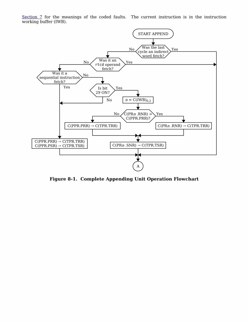
Section 7 for the meanings of the coded faults. The current instruction is in the instruction working buffer (IWB).
Figure 8-1. Complete Appending Unit Operation Flowchart
C(PPR.PRR) C(TPR.TRR)→C(PPR.PSR) C(TPR.TSR)→
START APPEND
YesNo
Yes
No
YesNo
A
Yes
No
YesNo
n = C(IWB)0,2
C(PPR.PRR) C(TPR.TRR)→ C(PRn .RNR) C(TPR.TRR)→
C(PRn .SNR) C(TPR.TSR)→
Was the lastcycle an indirect
word fetch?Was it an
rtcd operandfetch?
Was it asequential instruction
fetch?
C(PRn .RNR) >C(PPR.PRR)?
Is bit29 ON?

Figure 8-1(cont). Complete Appending Unit Operation Flowchart
A
YesNoYes
No
Yes No
Initiate adirected fault
Yes
No
Yes No
Initiate adirected fault
B
DSPTWcycle
MDSPTWcycle
PSDWcycle
NSDWcycle
Load SDWAM
C(SDW.R1) →C(RSDWH.R1)
DSBR.U= 0
is SDW forC(TPR.TSR)in SDWAM?
SDW.Fset ON?
DSPTW.Fset ON?
DSPTW.Uset ON?
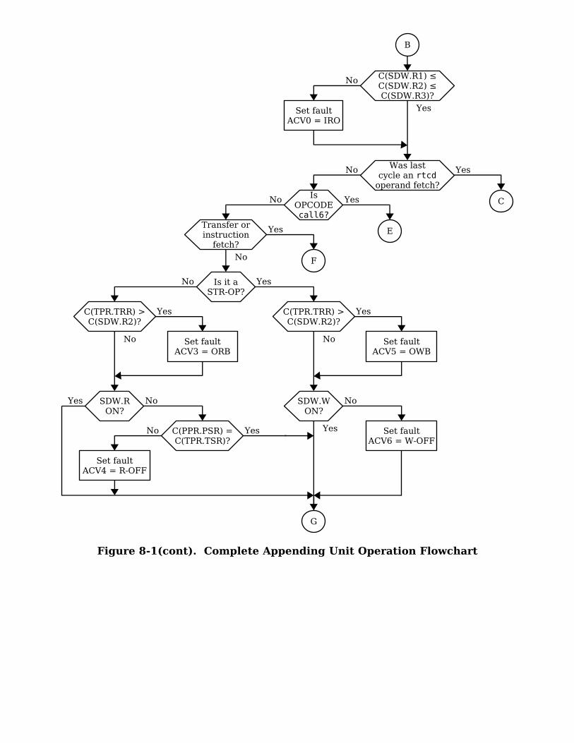
Figure 8-1(cont). Complete Appending Unit Operation Flowchart
B
Yes
No
YesNo
YesNo
Yes
No
C
E
F
YesNo
Yes
No
Yes
No
Yes
NoYes No
YesNo
G
Was lastcycle an rtcd
operand fetch?
Set faultACV0 = IRO
Set faultACV3 = ORB
Set faultACV5 = OWB
Set faultACV6 = W-OFF
Set faultACV4 = R-OFF
C(SDW.R1) ≤C(SDW.R2) ≤C(SDW.R3)?
IsOPCODEcall6?
Transfer orinstruction
fetch?
Is it aSTR-OP?
C(TPR.TRR) >C(SDW.R2)?
C(TPR.TRR) >C(SDW.R2)?
SDW.RON?
SDW.WON?
C(PPR.PSR) =C(TPR.TSR)?

Figure 8-1(cont). Complete Appending Unit Operation Flowchart
C
YesNo
Yes
No
Yes
No
No
(instruction fetch)D (rtcd operand)
Yes
No
Yes
NoYes
G
Set faultACV1 = OEB
Set faultACV2 = E-OFF
Set faultACV11 = INRET
Set faultACV13 = RALR
C(TPR.TRR) <C(SDW.R1)?
C(TPR.TRR) >C(SDW.R2)?
C(TPR.TRR) ≥C(PPR.PRR)
SDW.Eset ON?
RALR= 0?
C(PPR.PRR)< RALR?

Figure 8-1(cont). Complete Appending Unit Operation Flowchart
E
Yes
No
Yes
No
No
(call6)
Yes
G
Yes
No
Yes
No
No
Yes
No
Yes
Yes
No
Yes
No
Set faultACV2 = E-OFF
Set faultACV7 = NO GA
Set faultACV8 = OCB
Set faultACV9 = OCALL
Set faultACV10 = BOC
SDW.R2 C(TPR.TRR)→
SDW.Eset ON?
SDW.Gset ON?
C(PPR.PSR) =C(TPR.TSR)?
C(TPR.CA)4,17≥ SDW.CL?
C(TPR.TRR)> SDW.R3?
C(TPR.TRR)< SDW.R1?
C(TPR.TRR)> SDW.R2?
C(TPR.TRR) >C(PPR.PRR)?
C(PPR.PRR)< SDW.R2?

Figure 8-1(cont). Complete Appending Unit Operation Flowchart
(transfer or instruction fetch)
C(PPR.PRR) =C(TPR.TRR)?
F
Yes
No
YesNo
Yes
No
Yes
No
D
SDW.Eset ON?
C(TPR.TRR) >C(SDW.R2)?
C(TPR.TRR) <C(SDW.R1)?
Set faultACV1 = OEB
Set faultACV2 = E-OFF
Set faultACV12 = CRT

Figure 8-1(cont). Complete Appending Unit Operation Flowchart
G
YesNo
Yes
No
YesNo Initiate an accessviloation fault
Yes No
I
H
Yes No
Yes
No
Initiate adirected fault
Yes No
Initiate adirected fault
C(TPR.CA)0,13> SDW.BOUND?
is segmentC(TPR.TSR)
paged?
Any ACVfaults?
Is PTW.Fset ON?
PrepageMode?
Is PTW.Fset ON?
is PTW forC(TPR.CA)in PTWAM?
Set faultACV15 = OOSB
PTWcycle
PTW2cycle
LoadPTWAM

Figure 8-1(cont). Complete Appending Unit Operation Flowchart
I
Yes
No
Yes
No
J
No
H
Yes
No
K Yes
No
N Yes
L
No
Yes
END APPEND
MPTWcycle
FAPcycle
FANPcycle
Load/storeAPU data
STR-OP &PTW.M = 0?
Was thisan indirectword fetch?
Was it anrtcd operand
fetch?
Is OPCODEcall6?
Transfer orinstruction
fetch?
APU datamovement?
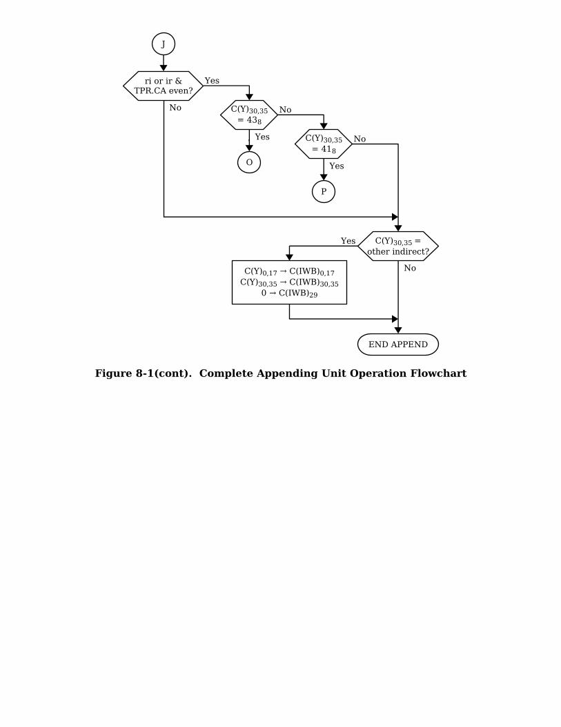
Figure 8-1(cont). Complete Appending Unit Operation Flowchart
Yes
No
No
J
Yes
No
O Yes
No
P
Yes
END APPEND
C(Y)0,17 C(IWB)→ 0,17C(Y)30,35 C(IWB)→ 30,35
0 C(IWB)→ 29
C(Y)30,35= 438
C(Y)30,35= 418
ri or ir &TPR.CA even?
C(Y)30,35 =other indirect?
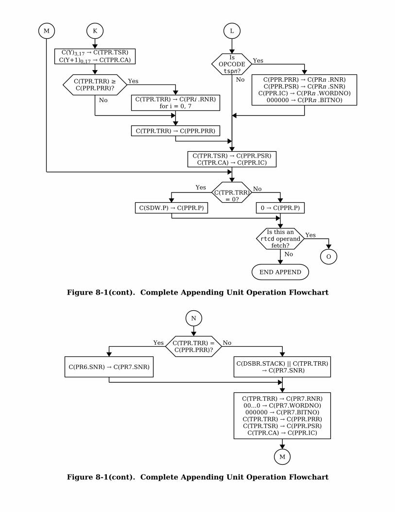
Figure 8-1(cont). Complete Appending Unit Operation Flowchart
Figure 8-1(cont). Complete Appending Unit Operation Flowchart
L
Yes
M K
No
Yes
No
Yes No
Yes
No O
END APPEND
C(Y)3,17 C(TPR.TSR)→C(Y+1)0,17 C(TPR.CA)→
C(TPR.TRR) C(PR→ i .RNR)for i = 0, 7
C(TPR.TRR) C(PPR.PRR)→
C(TPR.TSR) C(PPR.PSR)→C(TPR.CA) C(PPR.IC)→
C(SDW.P) C(PPR.P)→ 0 C(PPR.P)→
C(PPR.PRR) C(PR→ n .RNR)C(PPR.PSR) C(PR→ n .SNR)
C(PPR.IC) C(PR→ n .WORDNO)000000 C(PR→ n .BITNO)
IsOPCODEtspn?
C(TPR.TRR) ≥C(PPR.PRR)?
C(TPR.TRR)= 0?
Is this anrtcd operand
fetch?
Yes
N
No
M
C(TPR.TRR) =C(PPR.PRR)?
C(PR6.SNR) C(PR7.SNR)→C(DSBR.STACK) || C(TPR.TRR)
→ C(PR7.SNR)
C(TPR.TRR) C(PR7.RNR)→00...0 C(PR7.WORDNO)→000000 C(PR7.BITNO)→
C(TPR.TRR) C(PPR.PRR)→C(TPR.TSR) C(PPR.PSR)→
C(TPR.CA) C(PPR.IC)→

Figure 8-1(cont). Complete Appending Unit Operation Flowchart
Yes
O
No
Yes
NoYesNo
END APPEND
Yes
P
No
Yes
NoYesNo
END APPEND
C(TPR.TRR) ≥C(Y)18,20?
C(Y)18,20 ≥RSDWH.R1?
C(TPR.TRR) ≥RSDWH.R1?
C(PRn .RNR) ≥RSDWH.R1?
C(TPR.TRR) ≥C(PRn .RNR)?
C(TPR.TRR) ≥RSDWH.R1?
RSDWH.R1 C(TPR.TRR)→ C(Y)18,20 C(TPR.TRR)→
RSDWH.R1 C(TPR.TRR)→ C(PRn .RNR) C(TPR.TRR)→
SECTION 9: DPS/L68 CACHE MEMORY OPERATION
The Multics processor may be fitted with an optional cache memory. The operation of this cache memory is described in this section.
PHILOSOPHY OF CACHE MEMORY
The cache memory is a high speed buffer memory located within the processor that is intended to hold operands and/or instructions in expectation of their immediate use. This concept is different from that of holding a single operand (such as the divisor for a divide instruction) in the processor during execution of a single instruction. A cache memory depends on the locality of reference principle. Locality of reference involves the calculation of the probability, for any value of d, that the next instruction or operand reference after a reference to the instruction or operand at location A is to location A+d.
The calculation of probabilities for a set of values of d requires the statistical analysis of large volumes of real and simulated instruction sequences and data organizations. If it can be shown that the average expected data/instruction access time reduction (over the range 1 to d) is statistically significant in comparison to the fixed main memory access time, then the implementation of a cache memory with block size d will contribute a significant improvement in performance.
The results of such studies for the Multics processor with a cache memory as described below (with d!=!4) show a hit probability ranging between 80 and 95 percent (depending on instruction mix and data organization) and a performance improvement ranging up to 30 percent.
CACHE MEMORY ORGANIZATION
The cache memory is implemented as 2048 36-bit words of high-speed register storage with associated control and content directory circuitry within the processor. It is fully integrated with the normal data path circuitry and is virtually invisible to all programming sequences. Parity is generated, stored, and/or checked on each data reference. The total storage is divided into 512 blocks of 4 words each and the blocks are organized into 128 columns of four levels each.
Cache Memory / Main Memory Mapping
Main memory is mapped into the cache memory as described below and shown in Figure 9-1.
Main memory is divided into N blocks of 4 words each arranged in ascending order and numbered with the value of Y15,21 of the first word of the block.
All main memory blocks with numbers n modulo 128 are grouped associatively with cache memory column n.
Each cache memory column may hold any four blocks of the associated set of main memory blocks.
Each cache memory column has associated with it a four entry directory (one entry for each level) and a 2-bit round robin counter. Parity is generated, stored, and checked on each directory entry.
A cache directory entry consists of a 15-bit ADDRESS register, a pre-set, 2-bit level number value and a level full flag bit.
When a main memory block is loaded into a cache memory block at some level in the associated column, the directory ADDRESS register for that column and level is loaded with Y0,14. (Level selection is discussed in "Cache Memory Control" later in this section.)
Figure 9-1. Main Memory/Cache Memory Mapping
Cache Memory Addressing
For a read operation, the 24-bit absolute main memory address prepared by the appending unit is presented simultaneously to the cache control and to the main memory port selection circuitry. While port selection is being accomplished, the cache memory is accessed as follows.
Yl5,21 are used to select a cache memory column.
Block0
Words0,3
Block1
Words4,7
Block2
Words8,11
Block126
Words504,507
Block127
Words508,511
Block128
Words512,515
Block129
Words516,519
Block130
Words520,523
Block254
Words1016,1019
Block255
Words1020,1023
. . .
. . .
BlockN-128Words
-512,-509
BlockN-127Words
-508,-505
BlockN-126Words
-504,-501
BlockN-2
Words-8,-5
BlockN-1
Words-4,-1
. . .
. . .. . .. . .. . . . . .. . .
Column0
Level0
. . .
Column1
Level0
Column2
Level0
Column126
Level0
Column127
Level0
Column0
Level3
. . .
Column1
Level3
Column2
Level3
Column126
Level3
Column127
Level3
Column0
Level1
. . .
Column1
Level1
Column2
Level1
Column126
Level1
Column127
Level1
Column0
Level2
. . .
Column1
Level2
Column2
Level2
Column126
Level2
Column127
Level2
MainMemory
CacheMemory
. . .
Y0,14 are matched associatively against the four directory ADDRESS registers for the selected column.
If a match occurs for a level whose full flag is ON, a hit is signaled, the main memory reference cycle is canceled, and the level number value is read out.
The level number value and Y22,23 are used to select the level and word in the selected column and the cache memory data is read out into the data circuitry.
If no hit is signaled, the main memory reference cycle proceeds and a cache memory block load cycle is initiated (see "Cache Memory Control" below).
For a write operation, the 24-bit absolute main memory address prepared by the appending unit is presented simultaneously to the cache control and to the main memory port selection circuitry. While port selection is being accomplished, the cache memory is accessed as follows.
Y15,21 are used to select a cache memory column.
Y0,14 are matched associatively against the four directory ADDRESS registers for the selected column.
If a match occurs for a level whose full flag is ON, a hit is signaled and the level number value is read out.
The level number value and Y22,23 are used to select the level and word in the selected column, a cache memory write cycle is enabled, and the data is written to the main memory and the cache memory simultaneously.
If no hit is signaled, the main memory reference cycle proceeds with no further cache memory action.

CACHE MEMORY CONTROL
Enabling and Disabling Cache Memory
The cache memory is controlled by the state of several bits in the cache mode register (see Section 3). The cache mode register may be loaded with the Load Central Processor Register (lcpr) instruction. The cache memory control bits are as follows:
bit Value Action
54 0 The lower half of the cache memory (levels 0 and 1) is disabled.
1 The lower half of the cache memory is active and enabled as per the state of bits 56-57.
55 0 The upper half of the cache memory (levels 2 and 3) is disabled.
1 The upper half of the cache memory is active and enabled as per the state of bits 56-57.
56 0 The cache memory (if active) is not used for operands and indirect words.
1 The cache memory (if active) is used for operands and indirect words.
57 0 The cache memory (if active) is not used for instructions.
1 The cache memory (if active) is used for instructions.
59 0 The cache-to-register mode is not in effect (see "Dumping the Cache Memory" later in this section).
1 The cache-to-register mode is in effect.
NOTE: The cache memory option furnishes a switch panel maintenance aid that attaches to the free edge of the cache memory control logic board. The switch panel provides six switches for manual control of the cache memory:
Four of the switches inhibit the control functions of bits 54-57 of the cache mode register and have the effect of forcing the corresponding function to be disabled.
The fifth switch inhibits the store-aside feature wherein the processor is permitted to proceed immediately after the cache memory write cycle on write operations without waiting for a data acknowledgment from main memory. (There is no software control corresponding to this switch).
The sixth switch forces the enabled condition on all cache memory controls (except cache-to-register mode) without regard to the corresponding cache mode register control bit.
There is no switch corresponding to the cache-to-register control bit.
While these switches are intended primarily for maintenance sessions, they have been found useful in testing the cache memory during normal operation and in permitting operation of the processor with the cache memory in degraded or partially disabled mode.
Cache Memory Control in Segment Descriptor Words
Certain data have characteristics such that they should never be loaded into the cache memory. Primary examples of such data are hardware mailboxes for the I/O multiplexer, bulk store controller, etc., status return words, and various dynamic operating system data base segments. In general, any data that is modified by an agency external to a processor with the intent to convey information to that processor should never be loaded into cache memory.

Bit 57 of the segment descriptor word is used to reflect this property of "encacheability" for each segment. (See Section 5 for a discussion of the segment descriptor word.) If the bit is set ON, data from the segment may be loaded into the cache memory; if the bit is OFF, they may not. The operating system may set bit 57 ON or OFF as appropriate for the use of the segment.
Loading the Cache Memory
The cache memory is loaded with data implicitly whenever a cache memory block load is required. (See the discussion of read operations in "Cache Memory Addressing" earlier in this section.) There is no explicit method or instruction to load data into the cache memory.
When a cache memory block load is required, the level is selected from the value of the round robin counter for the selected column, and the cache memory write function is enabled. (The round robin counter contains the number of the least recently loaded level.) When the data arrives from main memory, it is written into the cache memory and entered into the data circuitry. The processor proceeds with the execution of the instruction requiring the operand if appropriate.
When the cache memory write is complete, further virtual address formation is inhibited, Y22 is inverted, and a second main memory access for the other half of the block is made. When the second half data arrives from main memory, it is written into the cache memory, Y0,14 are loaded into the directory ADDRESS register, the level full flag is set ON, the round robin counter is advanced by 1, and virtual address formation is permitted to proceed.
If all four level full flags for a column are set ON, a column full flag is also set ON and remains ON until one or more levels in the column are cleared.
Clearing the Cache Memory
Cache memory can be cleared in two ways; general clear and selective clear. The clearing action is the same in both cases, namely, the full flags of the selected column(s) and/or level(s) are set OFF.
General Clear
The entire cache memory is cleared by setting all column and level full flags to OFF in the following situations:
Upper or lower cache memory or both becoming enabled by appropriate bits in the operand of the Load Central Processor Register (lcpr) instruction or by action of the cache memory control logic board free edge switches.
Execution of a Clear Associative Memory Segments (cams) instruction with bit 15 of the address field set ON.
Selective Clear
The cache memory is cleared selectively as follows:
If a read-and-clear operation (ldac, sznc, etc.) results in a hit on the cache memory, that cache memory block hit is cleared.
Execution of a Clear Associative Memory Pages (camp) instruction with address bit 15 set ON causes Y13,14 to be matched against all cache directory ADDRESS registers. All cache memory blocks hit are cleared.

Dumping the Cache Memory
When the cache-to-register mode flag (bit 59 of the cache mode register) is set ON, the processor is forced to fetch the operands of all double-precision operations unit load operations from the cache memory. Y0,12 are ignored, Y15,21 select a column, and Y13,14 select a level. All other operations (e.g., instruction fetches, single-precision operands, etc.) are treated normally.
Note that the phrase "treated normally" as used here includes the case where the cache memory is enabled. If the cache memory is enabled, the "other" operations causes normal block loads and cache memory writes thus destroying the original contents of the cache memory. The cache memory should be disabled before dumping is attempted.
An indexed program loop involving the ldaq and staq instructions with the cache-to-register mode bit set ON serves to dump any or all of the cache memory.
The occurrence of a fault or interrupt sets the cache-to-register mode bit to OFF.

APPENDIX A: OPERATION CODE MAP
This appendix contains the operation code map for the processor in Figure A-1. The second portion of the map includes extended instruction set (EIS) instructions. Also see Appendix B for an alphabetical instruction list.

OPERATION CODE MAP (BIT 27 = 0)
000 001 002 003 004 005 006 007 010 011 012 013 014 015 016 017
000020040060
adlx0asx0adx0
mmeadlx1asx1adx1
drladlx2asx2adx2
adlx3asx3adx3
mme2adlx4asx4adx4
mme3adlx5asx5adx5
adlx6asx6adx6
mme4adlx7asx7adx7
adwp0
nop
adwp1awca
puls1ldqcadwp2awcq
puls2adladwp3lreg
ldacaos
ciocadlaasaada
adlqasqadq
adlaqsscradaq
100120140160
cmpx0sblx0ssx0sbx0
cmpx1sblx1ssx1sbx1
cmpx2sblx2ssx2sbx2
cmpx3sblx3ssx3sbx3
cmpx4sblx4ssx4sbx4
cmpx5sblx5ssx5sbx5
cmpx6sblx6ssx6sbx6
cmpx7sblx7ssx7sbx7
adwp4
cwl
adwp5swca
adwp6swcq
adwp7lpri
sdbr
cmpasblassasba
cmpqsblqssqsbq
cmpaqsblaq
sbaq
200220240260
cnax0ldx0orsx0orx0
cnax1ldx1orsx1orx1
cnax2ldx2orsx2orx2
cnax3ldx3orsx3orx3
cnax4ldx4orsx4orx4
cnax5ldx5orsx5orx5
cnax6ldx6orsx6orx6
cnax7ldx7orsx7orx7
lbarspri0tsp0
cmkrswspbp1tsp1
absaldbrspri2tsp2
epaqrmcmspbp3tsp3
szncsznspri
cnaaldaorsaora
cnaqldqorsqorq
cnaaqldaqlsdporaq
300320340360
canx0lcx0ansx0anx0
canx1lcx1ansx1anx1
canx2lcx2ansx2anx2
canx3lcx3ansx3anx3
canx4lcx4ansx4anx4
canx5lcx5ansx5anx5
canx6lcx6ansx6anx6
canx7lcx7ansx7anx7
eawp0eawp4epp0epp4
easp0easp4epbp1epbp5
eawp2eawp6epp2epp6
easp2easp6epbp3epbp7
stac
canalcaansaana
canqlcqansqanq
canaqlcaqstcdanaq
400420440460
sxl0
mpfufmsxl1fmp
mpy
sxl2dufmsxl3dfmp
sxl4
cmgfcmgsxl5 sxl6
dfcmgsxl7
fsznstzfstr
ldefldsmicfrd
scprdfstr
rscrdfld
dfrdstt
adeufafstfad
stedufadfstdfad
500520540560
rplrptsprp0rpd
sprp1 sprp2 sprp3 sprp4
bcdfdisprp5fdv
div
sprp6
dvfdfdisprp7dfdv
sbarnegstba
camsstbq
fnegneglsmcmfno
stc1
fcmpufs
fsb
dfcmpdufsssdpdfsb
600620640660
tzeeax0ersx0erx0
tnzeax1ersx1erx1
tnceax2ersx2erx2
trceax3ersx3erx3
tmieax4ersx4erx4
tpleax5ersx5erx5
eax6ersx6erx6
ttfeax7ersx7erx7
rtcdretspri4tsp4
spbp5tsp5
spri6tsp6
rcurcclspbp7tsp7
teoldistacqlcpr
teueaaersaera
diseaqersqerq
tovldtscueraq
700720740760
tsx0lxl0stx0lprp0
tsx1lxl1stx1lprp1
tsx2lxl2stx2lprp2
tsx3lxl3stx3lprp3
tsx4lxl4stx4lprp4
tsx5lxl5stx5lprp5
tsx6lxl6stx6lprp6
tsx7lxl7stx7lprp7
tra
stc2arsstcaarl
qrsstcqqrl
call6lrssreglrl
stigtb
tssalsstaalr
xecqlsstqqlr
xedllsstaqllr
Figure A-1. Processor Operation Code Map
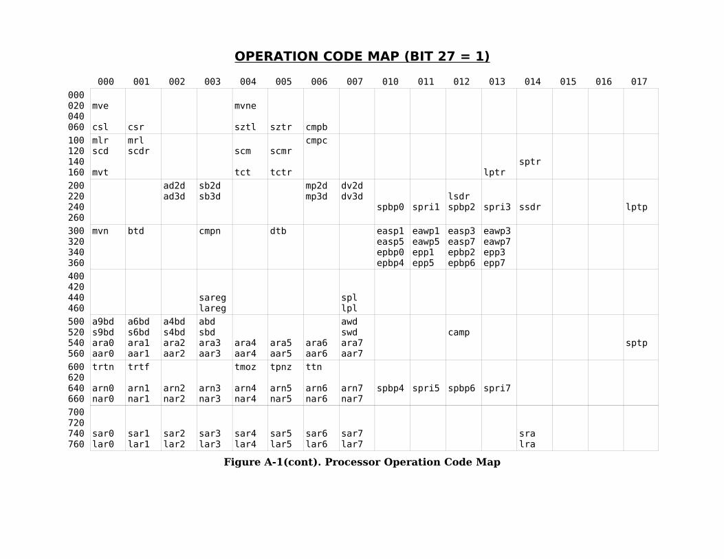
OPERATION CODE MAP (BIT 27 = 1)
000 001 002 003 004 005 006 007 010 011 012 013 014 015 016 017
000020040060
mve
csl csr
mvne
sztl sztr cmpb
100120140160
mlrscd
mvt
mrlscdr scm
tct
scmr
tctr
cmpc
lptrsptr
200220240260
ad2dad3d
sb2dsb3d
mp2dmp3d
dv2ddv3d
spbp0 spri1lsdrspbp2 spri3 ssdr lptp
300320340360
mvn btd cmpn dtb easp1easp5epbp0epbp4
eawp1eawp5epp1epp5
easp3easp7epbp2epbp6
eawp3eawp7epp3epp7
400420440460
sareglareg
spllpl
500520540560
a9bds9bdara0aar0
a6bds6bdara1aar1
a4bds4bdara2aar2
abdsbdara3aar3
ara4aar4
ara5aar5
ara6aar6
awdswdara7aar7
campsptp
600620640660
trtn
arn0nar0
trtf
arn1nar1
arn2nar2
arn3nar3
tmoz
arn4nar4
tpnz
arn5nar5
ttn
arn6nar6
arn7nar7
spbp4 spri5 spbp6 spri7
700720740760
sar0lar0
sar1lar1
sar2lar2
sar3lar3
sar4lar4
sar5lar5
sar6lar6
sar7lar7
sralra
Figure A-1(cont). Processor Operation Code Map

APPENDIX B: ALPHABETIC OPERATION CODE LIST
This appendix presents a listing of all processor instruction operation codes sorted alphabetically on mnemonic. It also includes the micro operations required by the mve and mvne edit instructions. The columns from left to right list the mnemonic, octal operation code value, the functional class, the page number in Section 4 of the instruction description, and the instruction name.
The functional class codes are:
FIX Fixed Point
BOOL Boolean Operations
FLT Floating Point
PREG Pointer Register
PRIV Privileged
MISC Miscellaneous
EIS Extended Instruction Set
TXFR Transfer of Control
MOP EIS Micro Operations
Mnemonic Code Class Page Name
a4bd 502 (1) EIS 225 Add 4-bit Displacement to Address Registera6bd 501 (1) EIS 226 Add 6-bit Displacement to Address Registera9bd 500 (1) EIS 226 Add 9-bit Displacement to Address Registeraar n 56n (1) EIS 219 Alphanumeric Descriptor to Address Register nabd 503 (1) EIS 227 Add Bit Displacement to Address Registerabsa 212 (0) PRIV 218 Absolute Address to A-Registerad2d 202 (1) EIS 265 Add Using Two Decimal Operandsad3d 222 (1) EIS 267 Add Using Three Decimal Operandsada 075 (0) FIX 111 Add to Aadaq 077 (0) FIX 111 Add to AQade 415 (0) FLT 160 Add to Exponentadl 033 (0) FIX 111 Add Low to AQadla 035 (0) FIX 112 Add Logical to Aadlaq 037 (0) FIX 112 Add Logical to AQadlq 036 (0) FIX 112 Add Logical to Qadlx n 02n (0) FIX 113 Add Logical to Index Register nadq 076 (0) FIX 113 Add to Qadwp0 050 (0) PREG 178 Add to Word Number of Pointer Register 0adwp1 051 (0) PREG 178 Add to Word Number of Pointer Register 1adwp2 052 (0) PREG 178 Add to Word Number of Pointer Register 2adwp3 053 (0) PREG 178 Add to Word Number of Pointer Register 3adwp4 150 (0) PREG 178 Add to Word Number of Pointer Register 4adwp5 151 (0) PREG 178 Add to Word Number of Pointer Register 5adwp6 152 (0) PREG 178 Add to Word Number of Pointer Register 6adwp7 153 (0) PREG 178 Add to Word Number of Pointer Register 7adx n 06n (0) FIX 113 Add to Index Register nalr 775 (0) FIX 107 A Left Rotateals 735 (0) FIX 107 A Left Shiftana 375 (0) BOOL 132 AND to Aanaq 377 (0) BOOL 132 AND to AQanq 376 (0) BOOL 132 AND to Qansa 355 (0) BOOL 132 AND to Storage A
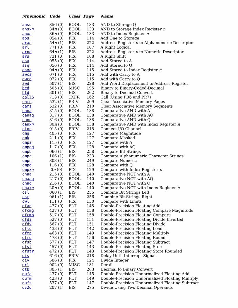
Mnemonic Code Class Page Name
ansq 356 (0) BOOL 133 AND to Storage Qansx n 34n (0) BOOL 133 AND to Storage Index Register nanx n 36n (0) BOOL 133 AND to Index Register naos 054 (0) FIX 114 Add One to Storageara n 54n (1) EIS 222 Address Register n to Alphanumeric Descriptorarl 771 (0) FIX 107 A Right Logicalarn n 64n (1) EIS 222 Address Register n to Numeric Descriptorars 731 (0) FIX 108 A Right Shiftasa 055 (0) FIX 114 Add Stored to Aasq 056 (0) FIX 114 Add Stored to Qasx n 04n (0) FIX 115 Add Stored to Index Register nawca 071 (0) FIX 115 Add with Carry to Aawcq 072 (0) FIX 115 Add with Carry to Qawd 507 (1) EIS 228 Add Word Displacement to Address Registerbcd 505 (0) MISC 195 Binary to Binary-Coded-Decimalbtd 301 (1) EIS 262 Binary to Decimal Convertcall6 713 (0) TXFR 162 Call (Using PR6 and PR7)camp 532 (1) PRIV 209 Clear Associative Memory Pagescams 532 (0) PRIV 210 Clear Associative Memory Segmentscana 315 (0) BOOL 138 Comparative AND with Acanaq 317 (0) BOOL 138 Comparative AND with AQcanq 316 (0) BOOL 138 Comparative AND with Qcanx n 30n (0) BOOL 138 Comparative AND with Index Register ncioc 015 (0) PRIV 215 Connect I/O Channelcmg 405 (0) FIX 127 Compare Magnitudecmk 211 (0) FIX 127 Compare Maskedcmpa 115 (0) FIX 127 Compare with Acmpaq 117 (0) FIX 128 Compare with AQcmpb 066 (1) EIS 258 Compare Bit Stringscmpc 106 (1) EIS 233 Compare Alphanumeric Character Stringscmpn 303 (1) EIS 249 Compare Numericcmpq 116 (0) FIX 128 Compare with Qcmpx n l0n (0) FIX 129 Compare with Index Register ncnaa 215 (0) BOOL 140 Comparative NOT with Acnaaq 217 (0) BOOL 140 Comparative NOT with AQcnaq 216 (0) BOOL 140 Comparative NOT with Qcnax n 20n (0) BOOL 140 Comparative NOT with Index Register ncsl 060 (1) EIS 255 Combine Bit Strings Leftcsr 061 (1) EIS 256 Combine Bit Strings Rightcwl 111 (0) FIX 130 Compare with Limitsdfad 477 (0) FLT 145 Double-Precision Floating Adddfcmg 427 (0) FLT 158 Double-Precision Floating Compare Magnitudedfcmp 517 (0) FLT 158 Double-Precision Floating Comparedfdi 527 (0) FLT 151 Double-Precision Floating Divide Inverteddfdv 567 (0) FLT 151 Double-Precision Floating Dividedfld 433 (0) FLT 142 Double-Precision Floating Loaddfmp 463 (0) FLT 149 Double-Precision Floating Multiplydfrd 473 (0) FLT 156 Double-Precision Floating Rounddfsb 577 (0) FLT 147 Double-Precision Floating Subtractdfst 457 (0) FLT 143 Double-Precision Floating Storedfstr 472 (0) FLT 143 Double-Precision Floating Store Roundeddis 616 (0) PRIV 218 Delay Until Interrupt Signaldiv 506 (0) FIX 124 Divide Integerdrl 002 (0) MISC 181 Deraildtb 305 (1) EIS 263 Decimal to Binary Convertdufa 437 (0) FLT 145 Double-Precision Unnormalized Floating Adddufm 423 (0) FLT 149 Double-Precision Unnormalized Floating Multiplydufs 537 (0) FLT 147 Double-Precision Unnormalized Floating Subtractdv2d 207 (1) EIS 275 Divide Using Two Decimal Operands

Mnemonic Code Class Page Name
dv3d 227 (1) EIS 276 Divide Using Three Decimal Operandsdvf 507 (0) FIX 124 Divide Fractioneaa 635 (0) FIX 94 Effective Address to Aeaq 636 (0) FIX 94 Effective Address to Qeasp0 311 (0) PREG 171 Effective Address to Segment Number of 0easp1 310 (1) PREG 171 Effective Address to Segment Number of PR1easp2 313 (0) PREG 171 Effective Address to Segment Number of PR2easp3 312 (1) PREG 171 Effective Address to Segment Number of PR3easp4 331 (0) PREG 171 Effective Address to Segment Number of PR4easp5 330 (1) PREG 171 Effective Address to Segment Number of PR5easp6 333 (0) PREG 171 Effective Address to Segment Number of PR6easp7 332 (1) PREG 171 Effective Address to Segment Number of PR7eawp0 310 (0) PREG 171 Effective Address to Word/Bit Number of PR0eawp1 311 (1) PREG 171 Effective Address to Word/Bit Number of PR1eawp2 312 (0) PREG 171 Effective Address to Word/Bit Number of PR2eawp3 313 (1) PREG 171 Effective Address to Word/Bit Number of PR3eawp4 330 (0) PREG 171 Effective to Word/Bit Number of PR4 Address eawp5 331 (1) PREG 171 Effective Address to Word/Bit Number of PR5eawp6 332 (0) PREG 172 Effective Address to Word/Bit Number of PR6eawp7 333 (1) PREG 172 Effective Address to Word/Bit Number of PR7eax n 62n (0) FIX 94 Effective Address to Index Register nepaq 213 (0) PREG 179 Effective Pointer to AQepbp0 350 (1) PREG 172 Effective Pointer at Base to Pointer Register 0epbp1 351 (0) PREG 172 Effective Pointer at Base to Pointer Register 1epbp2 352 (1) PREG 172 Effective Pointer at Base to Pointer Register 2epbp3 353 (0) PREG 172 Effective Pointer at Base to Pointer Register 3epbp4 370 (1) PREG 172 Effective Pointer at Base to Pointer Register 4epbp5 371 (0) PREG 172 Effective Pointer at Base to Pointer Register 5epbp6 372 (1) PREG 172 Effective Pointer at Base to Pointer Register 6epbp7 373 (0) PREG 172 Effective Pointer at Base to Pointer Register 7epp0 350 (0) PREG 173 Effective Pointer to Pointer Register 0epp1 351 (1) PREG 173 Effective Pointer to Pointer Register 1epp2 352 (0) PREG 173 Effective Pointer to Pointer Register 2epp3 353 (1) PREG 173 Effective Pointer to Pointer Register 3epp4 370 (0) PREG 173 Effective Pointer to Pointer Register 4epp5 371 (1) PREG 173 Effective Pointer to Pointer Register 5epp6 372 (0) PREG 173 Effective Pointer to Pointer Register 6epp7 373 (1) PREG 173 Effective Pointer to Pointer Register 7era 675 (0) BOOL 136 EXCLUSIVE OR to Aeraq 677 (0) BOOL 136 EXCLUSIVE OR to AQerq 676 (0) BOOL 136 EXCLUSIVE OR to Qersa 655 (0) BOOL 136 EXCLUSIVE OR to Storage Aersq 656 (0) BOOL 137 EXCLUSIVE OR to Storage Qersx n 64n (0) BOOL 137 EXCLUSIVE OR to Storage Index Register nerx n 66n (0) BOOL 137 EXCLUSIVE OR to Index Register nfad 475 (0) FLT 145 Floating Addfcmg 425 (0) FLT 158 Floating Compare Magnitudefcmp 515 (0) FLT 159 Floating Comparefdi 525 (0) FLT 152 Floating Divide Invertedfdv 565 (0) FLT 152 Floating Dividefld 431 (0) FLT 142 Floating Loadfmp 461 (0) FLT 149 Floating Multiplyfneg 513 (0) FLT 154 Floating Negatefno 573 (0) FLT 155 Floating Normalizefrd 471 (0) FLT 156 Floating Roundfsb 575 (0) FLT 147 Floating Subtractfst 455 (0) FLT 143 Floating Storefstr 470 (0) FLT 144 Floating Store Roundedfszn 430 (0) FLT 160 Floating Set Zero and Negative Indicators

Mnemonic Code Class Page Name
gtb 774 (0) MISC 196 Gray to Binarylareg 463 (1) EIS 220 Load Address Registerslar n 76n (1) EIS 219 Load Address Register nlbar 230 (0) FIX 197 Load Base Address Registerlca 335 (0) FIX 95 Load Complement Alcaq 337 (0) FIX 95 Load Complement AQlcpr 674 (0) PRIV 198 Load Central Processor Registerlcq 336 (0) FIX 95 Load Complement Qlcx n 32n (0) FIX 96 Load Complement Index Register nlda 235 (0) FIX 96 Load Aldac 034 (0) FIX 96 Load A and Clearldaq 237 (0) FIX 97 Load AQldbr 232 (0) PRIV 198 Load Descriptor Segment Base Registerlde 411 (0) FLT 160 Load Exponentldi 634 (0) FIX 97 Load Indicator Registerldq 236 (0) FIX 98 Load Qldqc 032 (0) FIX 98 Load Q and Clearldt 637 (0) PRIV 199 Load Timer Registerldx n 22n (0) FIX 99 Load Index Register nllr 777 (0) FIX 108 Long Left Rotatells 737 (0) FIX 108 Long Left Shiftlpl 467 (1) EIS 220 Load Pointers and Lengthslpri 173 (0) PREG 173 Load Pointer Registers from ITS Pairslprp n 76n (0) PREG 174 Load Pointer Register n Packedlptp 257 (1) PRIV 199 Load Page Table Pointerslptr 173 (1) PRIV 200 Load Page Table Registerslra 774 (1) PRIV 200 Load Ring Alarm Registerlreg 073 (0) FIX 99 Load Registerslrl 773 (0) FIX 109 Long Right Logicallrs 733 (0) FIX 109 Long Right Shiftlsdp 257 (0) PRIV 201 Load Segment Descriptor Pointerslsdr 232 (1) PRIV 201 Load Segment Descriptor Registerslxl n 72n (0) FIX 99 Load Index Register n from Lowermlr 100 (1) EIS 89 Move Alphanumeric Left to Rightmme 001 (0) MISC 184 Master Mode Entrymme2 004 (0) MISC 184 Master Mode Entry 2mme3 005 (0) MISC 185 Master Mode Entry 3mme4 007 (0) MISC 185 Master Mode Entry 4mp2d 206 (1) EIS 272 Multiply Using Two Decimal Operandsmp3d 226 (1) EIS 273 Multiply Using Three Decimal Operandsmpf 401 (0) FIX 122 Multiply Fractionmpy 402 (0) FIX 122 Multiply Integermrl 101 (1) EIS 244 Move Alphanumeric Right to Leftmve 020 (1) EIS 245 Move Alphanumeric Editedmvn 300 (1) EIS 251 Move Numericmvne 024 (1) EIS 253 Move Numeric Editedmvt 160 (1) EIS 247 Move Alphanumeric with Translationnar n 66n (1) EIS 220 Numeric Descriptor to Address Register nneg 531 (0) FIX 126 Negate Anegl 533 (0) FIX 126 Negate Longnop 011 (0) MISC 186 No Operationora 275 (0) BOOL 134 OR to Aoraq 277 (0) BOOL 134 OR to AQorq 276 (0) BOOL 134 OR to Qorsa 255 (0) BOOL 134 OR to Storage Aorsq 256 (0) BOOL 135 OR to Storage Qorsx n 24n (0) BOOL 135 OR to Storage Index Register norx n 26n (0) BOOL 135 OR to Index Register npuls1 012 (0) MISC 186 Pulse One

Mnemonic Code Class Page Name
puls2 013 (0) MISC 186 Pulse Twoqlr 776 (0) FIX 109 Q Left Rotateqls 736 (0) FIX 109 Q Left Shiftqrl 772 (0) FIX 110 Q Right Logicalqrs 732 (0) FIX 110 Q Right Shiftrccl 633 (0) MISC 180 Read Calendar Clockrcu 613 (0) PRIV 202 Restore Control Unitret 630 (0) TXFR 162 Returnrmcm 233 (0) PRIV 212 Read Memory Controller Mask Registerrpd 560 (0) MISC 187 Repeat Doublerpl 500 (0) MISC 189 Repeat Linkrpt 520 (0) MISC 191 Repeatrscr 413 (0) PRIV 212 Read System Controller Registerrsw 231 (0) PRIV 213 Read Switchesrtcd 610 (0) TXFR 163 Return Control Doubles4bd 522 (1) EIS 229 Subtract 4-bit Displacement from Address Registers6bd 521 (1) EIS 229 Subtract 6-bit Displacement from Address Registers9bd 520 (1) EIS 230 Subtract 9-bit Displacement from Address Registersareg 443 (1) EIS 223 Store Address Registerssar n 74n (1) EIS 223 Store Address Register nsb2d 203 (1) EIS 270 Subtract Using Two Decimal Operandssb3d 223 (1) EIS 271 Subtract Using Three Decimal Operandssba 175 (0) FIX 117 Subtract from Asbaq 177 (0) FIX 117 Subtract from AQsbar 550 (0) MISC 194 Store Base Address Registersbd 523 (1) EIS 231 Subtract Bit Displacement from Address Registersbla 135 (0) FIX 117 Subtract Logical from Asblaq 137 (0) FIX 118 Subtract Logical from AQsblq 136 (0) FIX 118 Subtract Logical from Qsblx n 12n (0) FIX 118 Subtract Logical from Index Register nsbq 176 (0) FIX 119 Subtract from Qsbx n 16n (0) FIX 119 Subtract from Index Register nscd 120 (1) EIS 234 Scan Characters Doublescdr 121 (1) EIS 236 Scan Characters Double in Reversescm 124 (1) EIS 237 Scan with Maskscmr 125 (1) EIS 238 Scan with Mask in Reversescpr 452 (0) PRIV 203 Store Central Processor Registerscu 657 (0) PRIV 204 Store Control Unitsdbr 154 (0) PRIV 204 Store Descriptor Segment Base Registersmcm 553 (0) PRIV 215 Set Memory Controller Mask Registersmic 451 (0) PRIV 215 Set Memory Controller interrupt Cellsspbp0 250 (1) PREG 175 Store Segment Base Pointer of Pointer Register 0spbp1 251 (0) PREG 175 Store Segment Base Pointer of Pointer Register 1spbp2 252 (1) PREG 175 Store Segment Base Pointer of Pointer Register 2spbp3 253 (0) PREG 175 Store Segment Base Pointer of Pointer Register 3spbp4 650 (1) PREG 175 Store Segment Base Pointer of Pointer Register 4spbp5 651 (0) PREG 175 Store Segment Base Pointer of Pointer Register 5spbp6 652 (1) PREG 175 Store Segment Base Pointer of Pointer Register 6spbp7 653 (0) PREG 175 Store Segment Base Pointer of Pointer Register 7spl 447 (1) EIS 223 Store Pointers and Lengthsspri 254 (0) PREG 175 Store Pointer Registers as ITS Pairsspri0 250 (0) PREG 176 Store Pointer Register 0 as ITS Pairspri1 251 (1) PREG 176 Store Pointer Register 1 as ITS Pairspri2 252 (0) PREG 176 Store Pointer Register 2 as ITS Pairspri3 253 (1) PREG 176 Store Pointer Register 3 as ITS Pairspri4 650 (0) PREG 176 Store Pointer Register 4 as ITS Pairspri5 651 (1) PREG 176 Store Pointer Register 5 as ITS Pairspri6 652 (0) PREG 176 Store Pointer Register 6 as ITS Pairspri7 653 (1) PREG 176 Store Pointer Register 7 as ITS Pair
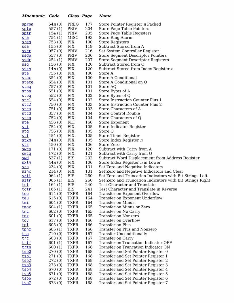
Mnemonic Code Class Page Name
sprp n 54n (0) PREG 177 Store Pointer Register n Packedsptp 557 (1) PRIV 204 Store Page Table Pointerssptr 154 (1) PRIV 205 Store Page Table Registerssra 754 (1) MISC 193 Store Ring Alarmsreg 753 (0) FIX 100 Store Registersssa 155 (0) FIX 119 Subtract Stored from Asscr 057 (0) PRIV 216 Set System Controller Registerssdp 557 (0) PRIV 206 Store Segment Descriptor Pointersssdr 254 (1) PRIV 207 Store Segment Descriptor Registersssq 156 (0) FIX 120 Subtract Stored from Qssx n 14n (0) FIX 120 Subtract Stored from Index Register nsta 755 (0) FIX 100 Store Astac 354 (0) FIX 100 Store A Conditionalstacq 654 (0) FIX 101 Store A Conditional on Qstaq 757 (0) FIX 101 Store AQstba 551 (0) FIX 101 Store Bytes of Astbq 552 (0) FIX 102 Store Bytes of Qstc1 554 (0) FIX 102 Store Instruction Counter Plus 1stc2 750 (0) FIX 103 Store Instruction Counter Plus 2stca 751 (0) FIX 103 Store Characters of Astcd 357 (0) FIX 104 Store Control Doublestcq 752 (0) FIX 104 Store Characters of Qste 456 (0) FLT 160 Store Exponentsti 754 (0) FIX 105 Store Indicator Registerstq 756 (0) FIX 105 Store Qstt 454 (0) FIX 105 Store Timer Registerstx n 74n (0) FIX 105 Store Index Register nstz 450 (0) FIX 106 Store Zeroswca 171 (0) FIX 120 Subtract with Carry from Aswcq 172 (0) FIX 121 Subtract with Carry from Qswd 527 (1) EIS 232 Subtract Word Displacement from Address Registersxl n 44n (0) FIX 106 Store Index Register n in Lowerszn 234 (0) FIX 131 Set Zero and Negative Indicatorssznc 214 (0) FIX 131 Set Zero and Negative Indicators and Clearsztl 064 (1) EIS 260 Set Zero and Truncation Indicators with Bit Strings Leftsztr 065 (1) EIS 260 Set Zero and Truncation Indicators with Bit Strings Righttct 164 (1) EIS 240 Test Character and Translatetctr 165 (1) EIS 241 Test Character and Translate in Reverseteo 614 (0) TXFR 164 Transfer on Exponent Overflowteu 615 (0) TXFR 164 Transfer on Exponent Underflowtmi 604 (0) TXFR 164 Transfer on Minustmoz 604 (1) TXFR 165 Transfer on Minus or Zerotnc 602 (0) TXFR 165 Transfer on No Carrytnz 601 (0) TXFR 165 Transfer on Nonzerotov 617 (0) TXFR 166 Transfer on Overflowtpl 605 (0) TXFR 166 Transfer on Plustpnz 605 (1) TXFR 166 Transfer on Plus and Nonzerotra 710 (0) TXFR 167 Transfer Unconditionallytrc 603 (0) TXFR 167 Transfer on Carrytrtf 601 (1) TXFR 167 Transfer on Truncation Indicator OFFtrtn 600 (1) TXFR 168 Transfer on Truncation Indicator ONtsp0 270 (0) TXFR 168 Transfer and Set Pointer Register 0tsp1 271 (0) TXFR 168 Transfer and Set Pointer Register 1tsp2 272 (0) TXFR 168 Transfer and Set Pointer Register 2tsp3 273 (0) TXFR 168 Transfer and Set Pointer Register 3tsp4 670 (0) TXFR 168 Transfer and Set Pointer Register 4tsp5 671 (0) TXFR 168 Transfer and Set Pointer Register 5tsp6 672 (0) TXFR 168 Transfer and Set Pointer Register 6tsp7 673 (0) TXFR 168 Transfer and Set Pointer Register 7

Mnemonic Code Class Page Name
tss 715 (0) TXFR 169 Transfer and Set Slavetsx n 70n (0) TXFR 169 Transfer and Set Index Register nttf 607 (0) TXFR 170 Transfer on Tally Runout Indicator OFFttn 606 (1) TXFR 170 Transfer on Tally Runout Indicator ONtze 600 (0) TXFR 170 Transfer on Zeroufa 435 (0) FLT 146 Unnormalized Floating Addufm 421 (0) FLT 150 Unnormalized Floating Multiplyufs 535 (0) FLT 148 Unnormalized Floating Subtractxec 716 (0) MISC 182 Executexed 717 (0) MISC 182 Execute Double
EIS Micro Operations
Mnemonic Code Class Page Name
cht 21 MOP 280 Change Tableenf 02 MOP 280 End Floating Suppressionign 14 MOP 281 Ignore Source Characterinsa 11 MOP 281 Insert Asterisk on Suppressioninsb 10 MOP 282 Insert Blank on Suppressioninsm 01 MOP 282 Insert Table Entry One Multipleinsn 12 MOP 282 Insert On Negativeinsp 13 MOP 283 Insert On Positivelte 20 MOP 283 Load Table Entrymflc 07 MOP 283 Move with Floating Currency Symbol Insertionmfls 06 MOP 284 Move with Floating Sign Insertionmors 17 MOP 284 Move and OR Signmses 16 MOP 285 Move and Set Signmvc 15 MOP 285 Move Source Charactersmvza 05 MOP 286 Move with Zero Suppression and Asterisk Replacementmvzb 04 MOP 286 Move with Zero Suppression and Blank Replacementses 03 MOP 287 Set End Suppression

APPENDIX C: ADDRESS MODIFIERS
00 01 02 03 04 05 06 07
0010 0
au1
qu2
du3
ic4
al5
ql6
dl7 r
2030
n*0*
au*1*
qu*2* 3*
ic*4*
al*5*
ql*6* 7* ri
4050
f1ci
itpi sc
itsad
sddi
scrdic
f2id
f3idc it
6070
*n*0
*au*1
*qu*2
*du*3
*ic*4
*al*5
*ql*6
*dl*7 ir
NONSTANDARD MODIFIERS
Instruction Tag Meaning
scpr 00 Store appending unit history register01 Store fault register
06 Store mode register10 Store decimal unit history register
20 Store control unit history register40 Store operations unit history register
lcpr 02 Load cache mode register
03 Load 0s into all history registers04 Load mode register
07 Load 1s into all history registers
stca See description in Section 4
stcq See description in Section 4
stba See description in Section 4
stbq See description in Section 4